JP5142037B2 - Belt member, transfer device, and image forming apparatus - Google Patents
Belt member, transfer device, and image forming apparatus Download PDFInfo
- Publication number
- JP5142037B2 JP5142037B2 JP2008190787A JP2008190787A JP5142037B2 JP 5142037 B2 JP5142037 B2 JP 5142037B2 JP 2008190787 A JP2008190787 A JP 2008190787A JP 2008190787 A JP2008190787 A JP 2008190787A JP 5142037 B2 JP5142037 B2 JP 5142037B2
- Authority
- JP
- Japan
- Prior art keywords
- belt
- layer
- image
- sec
- intermediate transfer
- Prior art date
- Legal status (The legal status is an assumption and is not a legal conclusion. Google has not performed a legal analysis and makes no representation as to the accuracy of the status listed.)
- Expired - Fee Related
Links
- 238000012546 transfer Methods 0.000 title claims description 128
- 239000010410 layer Substances 0.000 claims description 85
- 239000002344 surface layer Substances 0.000 claims description 57
- 239000006229 carbon black Substances 0.000 claims description 25
- 239000000428 dust Substances 0.000 description 28
- 206010047571 Visual impairment Diseases 0.000 description 26
- 229920001721 polyimide Polymers 0.000 description 21
- 239000000463 material Substances 0.000 description 20
- 229920005575 poly(amic acid) Polymers 0.000 description 19
- 239000006258 conductive agent Substances 0.000 description 18
- 230000000052 comparative effect Effects 0.000 description 17
- 238000000034 method Methods 0.000 description 17
- 238000002474 experimental method Methods 0.000 description 14
- 238000011156 evaluation Methods 0.000 description 13
- 238000000465 moulding Methods 0.000 description 13
- 230000002093 peripheral effect Effects 0.000 description 13
- 229920005989 resin Polymers 0.000 description 13
- 239000011347 resin Substances 0.000 description 13
- 239000004642 Polyimide Substances 0.000 description 12
- -1 polybutylene terephthalate Polymers 0.000 description 12
- 239000007787 solid Substances 0.000 description 11
- 238000001035 drying Methods 0.000 description 9
- 238000004519 manufacturing process Methods 0.000 description 9
- 238000005259 measurement Methods 0.000 description 9
- OKTJSMMVPCPJKN-UHFFFAOYSA-N Carbon Chemical compound [C] OKTJSMMVPCPJKN-UHFFFAOYSA-N 0.000 description 8
- 239000003795 chemical substances by application Substances 0.000 description 8
- 229910052751 metal Inorganic materials 0.000 description 8
- 239000002184 metal Substances 0.000 description 8
- 238000010586 diagram Methods 0.000 description 7
- 239000007788 liquid Substances 0.000 description 7
- 239000002245 particle Substances 0.000 description 7
- 239000009719 polyimide resin Substances 0.000 description 7
- 239000000126 substance Substances 0.000 description 7
- 229910052799 carbon Inorganic materials 0.000 description 6
- 238000000576 coating method Methods 0.000 description 6
- 229920001971 elastomer Polymers 0.000 description 6
- 238000007711 solidification Methods 0.000 description 6
- 230000008023 solidification Effects 0.000 description 6
- SECXISVLQFMRJM-UHFFFAOYSA-N N-Methylpyrrolidone Chemical compound CN1CCCC1=O SECXISVLQFMRJM-UHFFFAOYSA-N 0.000 description 5
- 150000004984 aromatic diamines Chemical class 0.000 description 5
- 125000003118 aryl group Chemical group 0.000 description 5
- 239000000203 mixture Substances 0.000 description 5
- YCKRFDGAMUMZLT-UHFFFAOYSA-N Fluorine atom Chemical compound [F] YCKRFDGAMUMZLT-UHFFFAOYSA-N 0.000 description 4
- XLOMVQKBTHCTTD-UHFFFAOYSA-N Zinc monoxide Chemical compound [Zn]=O XLOMVQKBTHCTTD-UHFFFAOYSA-N 0.000 description 4
- 238000004140 cleaning Methods 0.000 description 4
- 239000011248 coating agent Substances 0.000 description 4
- 230000007423 decrease Effects 0.000 description 4
- 238000001125 extrusion Methods 0.000 description 4
- 239000011737 fluorine Substances 0.000 description 4
- 229910052731 fluorine Inorganic materials 0.000 description 4
- 108091008695 photoreceptors Proteins 0.000 description 4
- 239000002798 polar solvent Substances 0.000 description 4
- 229920000642 polymer Polymers 0.000 description 4
- 239000002243 precursor Substances 0.000 description 4
- CBCKQZAAMUWICA-UHFFFAOYSA-N 1,4-phenylenediamine Chemical compound NC1=CC=C(N)C=C1 CBCKQZAAMUWICA-UHFFFAOYSA-N 0.000 description 3
- GWEVSGVZZGPLCZ-UHFFFAOYSA-N Titan oxide Chemical compound O=[Ti]=O GWEVSGVZZGPLCZ-UHFFFAOYSA-N 0.000 description 3
- 150000008065 acid anhydrides Chemical class 0.000 description 3
- WKDNYTOXBCRNPV-UHFFFAOYSA-N bpda Chemical compound C1=C2C(=O)OC(=O)C2=CC(C=2C=C3C(=O)OC(C3=CC=2)=O)=C1 WKDNYTOXBCRNPV-UHFFFAOYSA-N 0.000 description 3
- 150000001244 carboxylic acid anhydrides Chemical class 0.000 description 3
- 239000011247 coating layer Substances 0.000 description 3
- 239000003086 colorant Substances 0.000 description 3
- 238000010438 heat treatment Methods 0.000 description 3
- 125000005462 imide group Chemical group 0.000 description 3
- 150000002500 ions Chemical class 0.000 description 3
- 239000012948 isocyanate Substances 0.000 description 3
- 150000002513 isocyanates Chemical class 0.000 description 3
- 238000004898 kneading Methods 0.000 description 3
- 229920001084 poly(chloroprene) Polymers 0.000 description 3
- 229920001707 polybutylene terephthalate Polymers 0.000 description 3
- 238000006798 ring closing metathesis reaction Methods 0.000 description 3
- 239000002904 solvent Substances 0.000 description 3
- 150000005621 tetraalkylammonium salts Chemical class 0.000 description 3
- XOLBLPGZBRYERU-UHFFFAOYSA-N tin dioxide Chemical compound O=[Sn]=O XOLBLPGZBRYERU-UHFFFAOYSA-N 0.000 description 3
- 229910001887 tin oxide Inorganic materials 0.000 description 3
- VGGSQFUCUMXWEO-UHFFFAOYSA-N Ethene Chemical compound C=C VGGSQFUCUMXWEO-UHFFFAOYSA-N 0.000 description 2
- JOYRKODLDBILNP-UHFFFAOYSA-N Ethyl urethane Chemical compound CCOC(N)=O JOYRKODLDBILNP-UHFFFAOYSA-N 0.000 description 2
- 239000005977 Ethylene Substances 0.000 description 2
- PEDCQBHIVMGVHV-UHFFFAOYSA-N Glycerol Natural products OCC(O)CO PEDCQBHIVMGVHV-UHFFFAOYSA-N 0.000 description 2
- 229920001730 Moisture cure polyurethane Polymers 0.000 description 2
- 229920000459 Nitrile rubber Polymers 0.000 description 2
- 229920003171 Poly (ethylene oxide) Polymers 0.000 description 2
- 239000004962 Polyamide-imide Substances 0.000 description 2
- VYPSYNLAJGMNEJ-UHFFFAOYSA-N Silicium dioxide Chemical compound O=[Si]=O VYPSYNLAJGMNEJ-UHFFFAOYSA-N 0.000 description 2
- ATJFFYVFTNAWJD-UHFFFAOYSA-N Tin Chemical compound [Sn] ATJFFYVFTNAWJD-UHFFFAOYSA-N 0.000 description 2
- 229920006311 Urethane elastomer Polymers 0.000 description 2
- 239000006230 acetylene black Substances 0.000 description 2
- 229910000410 antimony oxide Inorganic materials 0.000 description 2
- 230000015572 biosynthetic process Effects 0.000 description 2
- 239000002131 composite material Substances 0.000 description 2
- 238000004132 cross linking Methods 0.000 description 2
- 230000002950 deficient Effects 0.000 description 2
- 235000014113 dietary fatty acids Nutrition 0.000 description 2
- 238000007598 dipping method Methods 0.000 description 2
- 239000002270 dispersing agent Substances 0.000 description 2
- 239000006185 dispersion Substances 0.000 description 2
- 239000013013 elastic material Substances 0.000 description 2
- 239000000194 fatty acid Substances 0.000 description 2
- 229930195729 fatty acid Natural products 0.000 description 2
- 239000000945 filler Substances 0.000 description 2
- 229910003437 indium oxide Inorganic materials 0.000 description 2
- PJXISJQVUVHSOJ-UHFFFAOYSA-N indium(iii) oxide Chemical compound [O-2].[O-2].[O-2].[In+3].[In+3] PJXISJQVUVHSOJ-UHFFFAOYSA-N 0.000 description 2
- 238000003475 lamination Methods 0.000 description 2
- 238000000691 measurement method Methods 0.000 description 2
- VNWKTOKETHGBQD-UHFFFAOYSA-N methane Chemical compound C VNWKTOKETHGBQD-UHFFFAOYSA-N 0.000 description 2
- 230000003287 optical effect Effects 0.000 description 2
- 239000003960 organic solvent Substances 0.000 description 2
- 229920002312 polyamide-imide Polymers 0.000 description 2
- 239000004417 polycarbonate Substances 0.000 description 2
- 229920000728 polyester Polymers 0.000 description 2
- 229920000139 polyethylene terephthalate Polymers 0.000 description 2
- 239000005020 polyethylene terephthalate Substances 0.000 description 2
- 238000006116 polymerization reaction Methods 0.000 description 2
- 229920001343 polytetrafluoroethylene Polymers 0.000 description 2
- 239000004810 polytetrafluoroethylene Substances 0.000 description 2
- 229920002635 polyurethane Polymers 0.000 description 2
- 239000004814 polyurethane Substances 0.000 description 2
- 229920002981 polyvinylidene fluoride Polymers 0.000 description 2
- 239000000843 powder Substances 0.000 description 2
- HNJBEVLQSNELDL-UHFFFAOYSA-N pyrrolidin-2-one Chemical compound O=C1CCCN1 HNJBEVLQSNELDL-UHFFFAOYSA-N 0.000 description 2
- 239000000523 sample Substances 0.000 description 2
- 239000000243 solution Substances 0.000 description 2
- 238000005507 spraying Methods 0.000 description 2
- 238000003756 stirring Methods 0.000 description 2
- 229910052718 tin Inorganic materials 0.000 description 2
- 230000032258 transport Effects 0.000 description 2
- 239000002966 varnish Substances 0.000 description 2
- 239000011787 zinc oxide Substances 0.000 description 2
- GEYOCULIXLDCMW-UHFFFAOYSA-N 1,2-phenylenediamine Chemical compound NC1=CC=CC=C1N GEYOCULIXLDCMW-UHFFFAOYSA-N 0.000 description 1
- WZCQRUWWHSTZEM-UHFFFAOYSA-N 1,3-phenylenediamine Chemical compound NC1=CC=CC(N)=C1 WZCQRUWWHSTZEM-UHFFFAOYSA-N 0.000 description 1
- VLDPXPPHXDGHEW-UHFFFAOYSA-N 1-chloro-2-dichlorophosphoryloxybenzene Chemical compound ClC1=CC=CC=C1OP(Cl)(Cl)=O VLDPXPPHXDGHEW-UHFFFAOYSA-N 0.000 description 1
- LXJLFVRAWOOQDR-UHFFFAOYSA-N 3-(3-aminophenoxy)aniline Chemical compound NC1=CC=CC(OC=2C=C(N)C=CC=2)=C1 LXJLFVRAWOOQDR-UHFFFAOYSA-N 0.000 description 1
- ZBMISJGHVWNWTE-UHFFFAOYSA-N 3-(4-aminophenoxy)aniline Chemical compound C1=CC(N)=CC=C1OC1=CC=CC(N)=C1 ZBMISJGHVWNWTE-UHFFFAOYSA-N 0.000 description 1
- ZDBWYUOUYNQZBM-UHFFFAOYSA-N 3-(aminomethyl)aniline Chemical compound NCC1=CC=CC(N)=C1 ZDBWYUOUYNQZBM-UHFFFAOYSA-N 0.000 description 1
- BFWYZZPDZZGSLJ-UHFFFAOYSA-N 4-(aminomethyl)aniline Chemical compound NCC1=CC=C(N)C=C1 BFWYZZPDZZGSLJ-UHFFFAOYSA-N 0.000 description 1
- HLBLWEWZXPIGSM-UHFFFAOYSA-N 4-Aminophenyl ether Chemical compound C1=CC(N)=CC=C1OC1=CC=C(N)C=C1 HLBLWEWZXPIGSM-UHFFFAOYSA-N 0.000 description 1
- VQVIHDPBMFABCQ-UHFFFAOYSA-N 5-(1,3-dioxo-2-benzofuran-5-carbonyl)-2-benzofuran-1,3-dione Chemical compound C1=C2C(=O)OC(=O)C2=CC(C(C=2C=C3C(=O)OC(=O)C3=CC=2)=O)=C1 VQVIHDPBMFABCQ-UHFFFAOYSA-N 0.000 description 1
- 229920001342 Bakelite® Polymers 0.000 description 1
- KWIUHFFTVRNATP-UHFFFAOYSA-N Betaine Natural products C[N+](C)(C)CC([O-])=O KWIUHFFTVRNATP-UHFFFAOYSA-N 0.000 description 1
- RYGMFSIKBFXOCR-UHFFFAOYSA-N Copper Chemical compound [Cu] RYGMFSIKBFXOCR-UHFFFAOYSA-N 0.000 description 1
- 229920002943 EPDM rubber Polymers 0.000 description 1
- 229920000877 Melamine resin Polymers 0.000 description 1
- FXHOOIRPVKKKFG-UHFFFAOYSA-N N,N-Dimethylacetamide Chemical compound CN(C)C(C)=O FXHOOIRPVKKKFG-UHFFFAOYSA-N 0.000 description 1
- 239000002033 PVDF binder Substances 0.000 description 1
- 239000004695 Polyether sulfone Substances 0.000 description 1
- 239000004698 Polyethylene Substances 0.000 description 1
- 239000004734 Polyphenylene sulfide Substances 0.000 description 1
- 239000004743 Polypropylene Substances 0.000 description 1
- 239000004793 Polystyrene Substances 0.000 description 1
- 229920001328 Polyvinylidene chloride Polymers 0.000 description 1
- 241000872198 Serjania polyphylla Species 0.000 description 1
- BLRPTPMANUNPDV-UHFFFAOYSA-N Silane Chemical compound [SiH4] BLRPTPMANUNPDV-UHFFFAOYSA-N 0.000 description 1
- GTDPSWPPOUPBNX-UHFFFAOYSA-N ac1mqpva Chemical compound CC12C(=O)OC(=O)C1(C)C1(C)C2(C)C(=O)OC1=O GTDPSWPPOUPBNX-UHFFFAOYSA-N 0.000 description 1
- 238000009825 accumulation Methods 0.000 description 1
- 229920000800 acrylic rubber Polymers 0.000 description 1
- XECAHXYUAAWDEL-UHFFFAOYSA-N acrylonitrile butadiene styrene Chemical compound C=CC=C.C=CC#N.C=CC1=CC=CC=C1 XECAHXYUAAWDEL-UHFFFAOYSA-N 0.000 description 1
- 239000004676 acrylonitrile butadiene styrene Substances 0.000 description 1
- 229920000122 acrylonitrile butadiene styrene Polymers 0.000 description 1
- 239000000853 adhesive Substances 0.000 description 1
- 230000001070 adhesive effect Effects 0.000 description 1
- 150000003973 alkyl amines Chemical class 0.000 description 1
- 150000008051 alkyl sulfates Chemical class 0.000 description 1
- 150000008052 alkyl sulfonates Chemical class 0.000 description 1
- 229910052782 aluminium Inorganic materials 0.000 description 1
- XAGFODPZIPBFFR-UHFFFAOYSA-N aluminium Chemical compound [Al] XAGFODPZIPBFFR-UHFFFAOYSA-N 0.000 description 1
- 150000003863 ammonium salts Chemical class 0.000 description 1
- WATWJIUSRGPENY-UHFFFAOYSA-N antimony atom Chemical compound [Sb] WATWJIUSRGPENY-UHFFFAOYSA-N 0.000 description 1
- 239000004637 bakelite Substances 0.000 description 1
- 229960003237 betaine Drugs 0.000 description 1
- 229910000416 bismuth oxide Inorganic materials 0.000 description 1
- 238000000071 blow moulding Methods 0.000 description 1
- 229920005549 butyl rubber Polymers 0.000 description 1
- 150000001718 carbodiimides Chemical class 0.000 description 1
- 239000000969 carrier Substances 0.000 description 1
- 230000015556 catabolic process Effects 0.000 description 1
- YACLQRRMGMJLJV-UHFFFAOYSA-N chloroprene Chemical compound ClC(=C)C=C YACLQRRMGMJLJV-UHFFFAOYSA-N 0.000 description 1
- 150000001875 compounds Chemical class 0.000 description 1
- 238000006482 condensation reaction Methods 0.000 description 1
- 239000011231 conductive filler Substances 0.000 description 1
- 229910052802 copper Inorganic materials 0.000 description 1
- 239000010949 copper Substances 0.000 description 1
- STZIXLPVKZUAMV-UHFFFAOYSA-N cyclopentane-1,1,2,2-tetracarboxylic acid Chemical compound OC(=O)C1(C(O)=O)CCCC1(C(O)=O)C(O)=O STZIXLPVKZUAMV-UHFFFAOYSA-N 0.000 description 1
- 230000018044 dehydration Effects 0.000 description 1
- 238000006297 dehydration reaction Methods 0.000 description 1
- 238000013461 design Methods 0.000 description 1
- 150000004985 diamines Chemical class 0.000 description 1
- TYIXMATWDRGMPF-UHFFFAOYSA-N dibismuth;oxygen(2-) Chemical compound [O-2].[O-2].[O-2].[Bi+3].[Bi+3] TYIXMATWDRGMPF-UHFFFAOYSA-N 0.000 description 1
- 238000007599 discharging Methods 0.000 description 1
- 230000000694 effects Effects 0.000 description 1
- 230000005684 electric field Effects 0.000 description 1
- 230000008030 elimination Effects 0.000 description 1
- 238000003379 elimination reaction Methods 0.000 description 1
- 229920005558 epichlorohydrin rubber Polymers 0.000 description 1
- 239000003822 epoxy resin Substances 0.000 description 1
- 229920000840 ethylene tetrafluoroethylene copolymer Polymers 0.000 description 1
- GBASTSRAHRGUAB-UHFFFAOYSA-N ethylenetetracarboxylic dianhydride Chemical compound O=C1OC(=O)C2=C1C(=O)OC2=O GBASTSRAHRGUAB-UHFFFAOYSA-N 0.000 description 1
- 150000002222 fluorine compounds Chemical class 0.000 description 1
- 229910002804 graphite Inorganic materials 0.000 description 1
- 239000010439 graphite Substances 0.000 description 1
- 239000012943 hotmelt Substances 0.000 description 1
- 238000003384 imaging method Methods 0.000 description 1
- 238000006358 imidation reaction Methods 0.000 description 1
- 229910052738 indium Inorganic materials 0.000 description 1
- APFVFJFRJDLVQX-UHFFFAOYSA-N indium atom Chemical compound [In] APFVFJFRJDLVQX-UHFFFAOYSA-N 0.000 description 1
- 238000001746 injection moulding Methods 0.000 description 1
- 238000009413 insulation Methods 0.000 description 1
- 229920003049 isoprene rubber Polymers 0.000 description 1
- 239000003273 ketjen black Substances 0.000 description 1
- MHCFAGZWMAWTNR-UHFFFAOYSA-M lithium perchlorate Chemical compound [Li+].[O-]Cl(=O)(=O)=O MHCFAGZWMAWTNR-UHFFFAOYSA-M 0.000 description 1
- 229910001486 lithium perchlorate Inorganic materials 0.000 description 1
- 229940018564 m-phenylenediamine Drugs 0.000 description 1
- JDSHMPZPIAZGSV-UHFFFAOYSA-N melamine Chemical compound NC1=NC(N)=NC(N)=N1 JDSHMPZPIAZGSV-UHFFFAOYSA-N 0.000 description 1
- 238000002844 melting Methods 0.000 description 1
- 230000008018 melting Effects 0.000 description 1
- 229910044991 metal oxide Inorganic materials 0.000 description 1
- 150000004706 metal oxides Chemical class 0.000 description 1
- 150000002739 metals Chemical class 0.000 description 1
- CWQXQMHSOZUFJS-UHFFFAOYSA-N molybdenum disulfide Chemical compound S=[Mo]=S CWQXQMHSOZUFJS-UHFFFAOYSA-N 0.000 description 1
- 229910052982 molybdenum disulfide Inorganic materials 0.000 description 1
- 239000002736 nonionic surfactant Substances 0.000 description 1
- VTRUBDSFZJNXHI-UHFFFAOYSA-N oxoantimony Chemical compound [Sb]=O VTRUBDSFZJNXHI-UHFFFAOYSA-N 0.000 description 1
- 229920002492 poly(sulfone) Polymers 0.000 description 1
- 229920000058 polyacrylate Polymers 0.000 description 1
- 229920000515 polycarbonate Polymers 0.000 description 1
- 229920005668 polycarbonate resin Polymers 0.000 description 1
- 239000004431 polycarbonate resin Substances 0.000 description 1
- 229920000647 polyepoxide Polymers 0.000 description 1
- 229920006393 polyether sulfone Polymers 0.000 description 1
- 229920000573 polyethylene Polymers 0.000 description 1
- 230000000379 polymerizing effect Effects 0.000 description 1
- 229920000306 polymethylpentene Polymers 0.000 description 1
- 239000011116 polymethylpentene Substances 0.000 description 1
- 229920000069 polyphenylene sulfide Polymers 0.000 description 1
- 229920001155 polypropylene Polymers 0.000 description 1
- 229920001296 polysiloxane Polymers 0.000 description 1
- 229920002223 polystyrene Polymers 0.000 description 1
- 229920005749 polyurethane resin Polymers 0.000 description 1
- 239000005033 polyvinylidene chloride Substances 0.000 description 1
- 239000002994 raw material Substances 0.000 description 1
- 230000000717 retained effect Effects 0.000 description 1
- 238000007363 ring formation reaction Methods 0.000 description 1
- 239000011163 secondary particle Substances 0.000 description 1
- 229910000077 silane Inorganic materials 0.000 description 1
- HBMJWWWQQXIZIP-UHFFFAOYSA-N silicon carbide Chemical compound [Si+]#[C-] HBMJWWWQQXIZIP-UHFFFAOYSA-N 0.000 description 1
- 229910010271 silicon carbide Inorganic materials 0.000 description 1
- 239000000377 silicon dioxide Substances 0.000 description 1
- 229920002379 silicone rubber Polymers 0.000 description 1
- 239000004945 silicone rubber Substances 0.000 description 1
- 239000002356 single layer Substances 0.000 description 1
- 239000007921 spray Substances 0.000 description 1
- 230000003068 static effect Effects 0.000 description 1
- 229920003048 styrene butadiene rubber Polymers 0.000 description 1
- 229920005992 thermoplastic resin Polymers 0.000 description 1
- 239000004408 titanium dioxide Substances 0.000 description 1
- OGIDPMRJRNCKJF-UHFFFAOYSA-N titanium oxide Inorganic materials [Ti]=O OGIDPMRJRNCKJF-UHFFFAOYSA-N 0.000 description 1
- 238000011144 upstream manufacturing Methods 0.000 description 1
Images


Classifications
-
- G—PHYSICS
- G03—PHOTOGRAPHY; CINEMATOGRAPHY; ANALOGOUS TECHNIQUES USING WAVES OTHER THAN OPTICAL WAVES; ELECTROGRAPHY; HOLOGRAPHY
- G03G—ELECTROGRAPHY; ELECTROPHOTOGRAPHY; MAGNETOGRAPHY
- G03G15/00—Apparatus for electrographic processes using a charge pattern
- G03G15/14—Apparatus for electrographic processes using a charge pattern for transferring a pattern to a second base
- G03G15/16—Apparatus for electrographic processes using a charge pattern for transferring a pattern to a second base of a toner pattern, e.g. a powder pattern, e.g. magnetic transfer
- G03G15/1605—Apparatus for electrographic processes using a charge pattern for transferring a pattern to a second base of a toner pattern, e.g. a powder pattern, e.g. magnetic transfer using at least one intermediate support
- G03G15/162—Apparatus for electrographic processes using a charge pattern for transferring a pattern to a second base of a toner pattern, e.g. a powder pattern, e.g. magnetic transfer using at least one intermediate support details of the the intermediate support, e.g. chemical composition
Landscapes
- Physics & Mathematics (AREA)
- General Physics & Mathematics (AREA)
- Electrostatic Charge, Transfer And Separation In Electrography (AREA)
Description
本発明は、プリンタ、ファクシミリ、複写機などの画像形成装置に用いられるベルト部材、転写装置、及び、それらを備えた画像形成装置に関するものである。 The present invention relates to a belt member used in an image forming apparatus such as a printer, a facsimile machine, and a copying machine, a transfer device, and an image forming apparatus including them.
この種の画像形成装置、とりわけフルカラー画像形成装置として次のようなものが知られている。すなわち、像担持体に対して中間転写ベルトのベルト外周面を接触させ、転写バイアス印加手段により形成される転写電界によって、像担持体上に形成されたトナー像を、中間転写ベルトのベルト外周面に1次転写する。そして、この中間転写ベルトのベルト外周面に1次転写されたトナー像を、ベルト外周面に沿って搬送される転写材上に2次転写して転写材上に画像形成を行うものである。 The following are known as this type of image forming apparatus, particularly as a full-color image forming apparatus. That is, the outer peripheral surface of the intermediate transfer belt is brought into contact with the image carrier, and the toner image formed on the image carrier is transferred to the outer peripheral surface of the intermediate transfer belt by the transfer electric field formed by the transfer bias applying unit. Primary transfer. Then, the toner image primarily transferred onto the outer peripheral surface of the intermediate transfer belt is secondarily transferred onto a transfer material conveyed along the outer peripheral surface of the belt to form an image on the transfer material.
特許文献1に記載の画像形成装置では、中間転写ベルトとして、トナー像を担持する側のベルト外周面を形成する高抵抗の表面層と、トナーの帯電極性とは逆極性の転写バイアスが印加される中間転写ベルトのベルト内周面を形成する中抵抗の基層とを有する多層構造の多層ベルトが用いられている。このように表面層を高抵抗とすることで表面層を中抵抗などにした場合よりも転写後の表面層に上記逆極性の電荷を多く残留させることができる。転写後の表面層に残留する上記逆極性の電荷が少ないと、ベルト外周面上に形成されたトナー像を静電的な力によってその場に留めておくことができなくなる。その結果、中間転写ベルトのベルト外周面上に一部のトナーが飛散し、この飛散したトナーがチリとなって画像品質に影響を及ぼすことがある。転写後の表面層に上記逆極性の電荷が多く残留することで、ベルト外周面に形成されたトナー像を静電的な力によってその場に留めることができ、上述のようなチリの発生が抑制することができるとされている。
In the image forming apparatus described in
ここで、従来から知られている定電流制御で行われる転写時においては、装置本体内の温度湿度環境等により中間転写ベルトなどの抵抗が変化することで転写時に印加するトナーの帯電極性とは逆極性の転写バイアスの大きさが異なり中間転写ベルトの帯電電位も異なってくる。 Here, at the time of transfer performed by the conventionally known constant current control, the resistance of the intermediate transfer belt or the like changes depending on the temperature and humidity environment in the apparatus main body, so that the charging polarity of the toner applied at the time of transfer is The size of the reverse polarity transfer bias is different, and the charging potential of the intermediate transfer belt is also different.
高温高湿環境では常温常湿度環境に比べ中間転写ベルトの抵抗が低くなり、定電流制御で行われる転写時に印加される転写バイアスが低くなって、中間転写ベルトの帯電電位が低くなる。また、中間転写ベルトの抵抗が低くなることで中間転写ベルトの表面層に残留する上記逆極性の電荷も常温常湿度環境のときに比べて少なくなる。そのため、中間転写ベルトの帯電電位が低くなるのに加えて、転写後に表面層に残留する上記逆極性の電荷が少なくなることで、ベルト外周面上に形成されたトナー像を静電的な力によってその場に留めにくくなり、チリが発生し易くなる。 In a high-temperature and high-humidity environment, the resistance of the intermediate transfer belt is lower than that in a normal temperature and normal humidity environment, the transfer bias applied during transfer performed by constant current control is lowered, and the charging potential of the intermediate transfer belt is lowered. Further, since the resistance of the intermediate transfer belt is lowered, the charge of the reverse polarity remaining on the surface layer of the intermediate transfer belt is reduced as compared with that in a normal temperature and humidity environment. Therefore, in addition to the charge potential of the intermediate transfer belt being lowered, the charge of the reverse polarity remaining on the surface layer after transfer is reduced, so that the toner image formed on the outer peripheral surface of the belt can be This makes it difficult to stay in place and makes it easy to generate dust.
低温低湿環境では常温常湿度環境に比べて中間転写ベルトの抵抗が高くなり、定電流制御で行われる転写時に印加される転写バイアスが高くなって、中間転写ベルトの帯電電位が高くなる。また、中間転写ベルトの抵抗が高くなることで中間転写ベルトの表面層に残留する上記逆極性の電荷も常温常湿度環境のときに比べて多くなる。そのため、中間転写ベルトの帯電電位が高くなるのに加えて転写後に表面層に残留する上記逆極性の電荷が多くなることで、ベルト外周面上に形成されたトナー像を静電的な力によってその場により留めることができ、チリの発生をより抑制することができる。ところが、転写後の表面層に残留する電荷が多くなる分、残像が発生し易くなる。 In the low temperature and low humidity environment, the resistance of the intermediate transfer belt is higher than that in the normal temperature and normal humidity environment, the transfer bias applied at the time of transfer performed by constant current control is increased, and the charging potential of the intermediate transfer belt is increased. Further, since the resistance of the intermediate transfer belt is increased, the charge of the reverse polarity remaining on the surface layer of the intermediate transfer belt is increased as compared with the normal temperature and humidity environment. For this reason, in addition to the charging potential of the intermediate transfer belt being increased, the charge of the reverse polarity remaining on the surface layer after transfer is increased, so that the toner image formed on the outer peripheral surface of the belt is electrostatically applied. It can be stopped on the spot and the generation of dust can be further suppressed. However, the amount of charge remaining on the surface layer after transfer increases, so that an afterimage is likely to occur.
このように、高抵抗の表面層と中抵抗からの基層とを有する多層構造の中間転写ベルトを用いたとしてもチリが発生するのを抑制できない場合があったり、さらには残像が発生してしまう場合があるといった問題が生じる。 As described above, even when a multi-layer intermediate transfer belt having a high-resistance surface layer and a medium-resistance base layer is used, the occurrence of dust may not be suppressed or an afterimage may be generated. The problem that there is a case arises.
本発明は以上の問題点に鑑みなされたものであり、その目的は、チリや残像などの発生を抑制できるベルト部材、転写装置及びそれらを備えた画像形成装置を提供することである。 The present invention has been made in view of the above problems, and an object thereof is to provide a belt member, a transfer device, and an image forming apparatus including the belt member that can suppress generation of dust and afterimages.
上記目的を達成するために、請求項1の発明は、画像形成装置に用いられる、トナー像を担持する高抵抗の表面層を有した多層構造のループ状のベルト部材において、ループ内側の面である裏面における表面抵抗率の500[V]印加時の10[sec]測定値が常用対数値[log(Ω/□)]で9.0〜12.5であり、ループ外側の面であるおもて面における表面抵抗率の100[sec]測定値と1[sec]測定値との差であるおもて面表面抵抗率変化量が、100[V]印加時に常用対数値[log(Ω/□)]で0.5〜1.50、及び、500[V]印加時に常用対数値[log(Ω/□)]で0.2以下であり、該裏面における表面抵抗率の100[sec]測定値と1[sec]測定値との差である裏面表面抵抗率変化量が、100[V]印加時及び500[V]印加時共に常用対数値[log(Ω/□)]で0.1以下であることを特徴とするものである。
また、請求項2の発明は、請求項1のベルト部材において、上記表面層には少なくともカーボンブラックが添加されていることを特徴とするものである。
また、請求項3の発明は、請求項1または2のベルト部材において、上記おもて面側及び上記裏面側に、電子導電性部材とイオン導電性部材とを含む層が設けられていることを特徴とするものである。
また、請求項4の発明は、潜像担持体上のトナー像が一時的に転写される中間転写体を備えた転写装置において、該中間転写体として、請求項1、2または3のベルト部材を用いることを特徴とするものである。
また、請求項5の発明は、潜像を担持する潜像担持体と、該潜像をトナー像に現像する現像手段と、該潜像担持体上のトナー像が一時的に転写される中間転写ベルトを有する転写手段とを備えた画像形成装置において、該転写手段として、請求項4の転写装置を用いることを特徴とするものである。
In order to achieve the above object, a first aspect of the present invention provides a multilayer belt-shaped belt member having a high-resistance surface layer for supporting a toner image, which is used in an image forming apparatus. The measured value of the surface resistivity on a certain back surface at 500 [V] is 10 to 12.5 in common logarithmic value [log (Ω / □)], which is the surface outside the loop. A change in front surface resistivity, which is the difference between a measured value of 100 [sec] and a measured value of 1 [sec] on the front surface, is a common logarithmic value [log (Ω / □)] is 0.5 to 1.50, and the logarithmic value [log (Ω / □)] is 0.2 or less when 500 [V] is applied, and the surface resistivity on the back surface is 100 [sec. ] Change in back surface resistivity, which is the difference between the measured value and 1 [sec] measured value And is characterized in that 100 [V] applied at and 500 [V] applied at both common logarithm [log (Ω / □)] is 0.1 or less.
According to a second aspect of the present invention, in the belt member of the first aspect, at least carbon black is added to the surface layer.
According to a third aspect of the present invention, in the belt member according to the first or second aspect, a layer including an electronic conductive member and an ion conductive member is provided on the front surface side and the back surface side. It is characterized by.
According to a fourth aspect of the present invention, there is provided a transfer apparatus comprising an intermediate transfer member to which a toner image on a latent image carrier is temporarily transferred. It is characterized by using.
According to a fifth aspect of the present invention, there is provided a latent image carrier that carries a latent image, a developing unit that develops the latent image into a toner image, and an intermediate on which the toner image on the latent image carrier is temporarily transferred. An image forming apparatus including a transfer unit having a transfer belt is characterized in that the transfer unit according to claim 4 is used as the transfer unit.
以上、本発明においては、画像形成装置に用いられる、トナー像を担持する高抵抗の表面層を有した多層構造のループ状のベルト部材において、ループ内側の面である裏面における表面抵抗率の500[V]印加時の10[sec]測定値が常用対数値[log(Ω/□)]で9.0〜12.5であり、ループ外側の面であるおもて面における表面抵抗率の100[sec]測定値と1[sec]測定値との差であるおもて面表面抵抗率変化量が、100[V]印加時に常用対数値[log(Ω/□)]で0.5〜1.5、及び、500[V]印加時に常用対数値[log(Ω/□)]で0.2以下であり、上記裏面における表面抵抗率の100[sec]測定値と1[sec]測定値との差である裏面表面抵抗率変化量が、100[V]印加時及び500[V]印加時共に常用対数値[log(Ω/□)]で0.1以下であることで、後述する実験で明らかにしたように、チリや残像などが発生するのを抑制できるという優れた効果がある。 As described above, in the present invention, in a loop-shaped belt member having a high-resistance surface layer for supporting a toner image, which is used in an image forming apparatus, a surface resistivity of 500 on the back surface which is the inner surface of the loop. The measured value of 10 [sec] at the time of applying [V] is 9.0 to 12.5 in the common logarithmic value [log (Ω / □)], and the surface resistivity of the front surface which is the outer surface of the loop The front surface resistivity change amount, which is the difference between the measured value of 100 [sec] and the measured value of 1 [sec], is 0.5 when the logarithmic value [log (Ω / □)] is used when 100 [V] is applied. The logarithmic value [log (Ω / □)] is 0.2 or less when applied to 1.5 and 500 [V], and the measured value of 100 [sec] and 1 [sec] of the surface resistivity on the back surface. Change in the back surface resistivity, which is the difference from the measured value, applied 100 [V] And 500 [V], the common logarithmic value [log (Ω / □)] is 0.1 or less, so that it is possible to suppress the occurrence of dust and afterimages as clarified in the experiment described later. There is an excellent effect.
以下、図面を参照しながら、本発明の一実施形態について説明する。図2は本発明の一実施形態を示す画像形成装置の概略構成図である。この画像形成装置の中央には、複数の支持ローラに掛け回された中間転写体である無端ベルト状の中間転写ベルト201を備えた転写装置200が設けられている。また、第1の支持ローラ202と第2の支持ローラ203との間に張り渡された中間転写ベルト201上には、その搬送方向に沿って、イエロー(Y)、マゼンタ(M)、シアン(C)、ブラック(Bk)の各色用の4つの画像形成部(画像形成ユニット)101Y,101M,101C,101Bkが横に並べて配置されており、これらの画像形成部(画像形成ユニット)101Y,101M,101C,101Bkはタンデム型画像形成部を構成している。このタンデム型画像形成部の各画像形成部101Y,101M,101C,101Bkの構成は同じであり、例えば図3に示すように構成されている。
Hereinafter, an embodiment of the present invention will be described with reference to the drawings. FIG. 2 is a schematic configuration diagram of an image forming apparatus showing an embodiment of the present invention. At the center of the image forming apparatus, there is provided a
図3はブラック(Bk)用の画像形成部101Bkを例に上げたものであり、この画像形成部101Bkには、像担持体であるドラム状の感光体102Bkと、該感光体にトナー像を形成するための画像形成手段を構成する帯電装置103Bk、露光装置110Bk、現像装置104Bkが設けられている。 FIG. 3 shows an example of an image forming unit 101Bk for black (Bk). In this image forming unit 101Bk, a drum-shaped photoconductor 102Bk which is an image carrier and a toner image on the photoconductor. A charging device 103Bk, an exposure device 110Bk, and a developing device 104Bk constituting an image forming unit for forming are provided.
露光装置110Bkは、図示の例では感光体102Bkの軸方向(主走査方向)に配置された発光ダイオード(LED)アレイとレンズアレイからなるLED書込み方式の露光装置であり、画像信号に応じてLEDを発光して感光体上に静電潜像を形成するものであるが、この他、レーザ光源と光偏向器(回転多面鏡等)と結像走査光学系からなるレーザ走査方式の露光装置を用いることができる。 In the illustrated example, the exposure device 110Bk is an LED writing type exposure device comprising a light emitting diode (LED) array and a lens array arranged in the axial direction (main scanning direction) of the photoconductor 102Bk. In addition to this, an electrostatic latent image is formed on the photosensitive member. In addition, a laser scanning type exposure apparatus comprising a laser light source, an optical deflector (rotating polygon mirror, etc.) and an imaging scanning optical system is provided. Can be used.
現像装置104Bkは、現像剤を担持して回転する現像ローラ(または現像スリーブ)と、現像剤を撹拌・搬送して現像ローラ(または現像スリーブ)に供給する撹拌・搬送部材等で構成され、感光体102Bk上に形成された静電潜像を現像剤のトナーで現像して可視像化する。現像剤としては、トナーのみからなる一成分現像剤、あるいはトナーと磁性キャリアからなる二成分現像剤が用いられる。なお、図3はブラック(Bk)用の画像形成部101Bkの例であるので、トナーには、ブラック色のトナーが用いられるが、図2に示す他の色の画像形成部101Y,101M,101Cでは、それぞれイエロー(Y)、マゼンタ(M)、シアン(C)の各色のトナーが用いられる。
The developing device 104Bk includes a developing roller (or developing sleeve) that carries and rotates the developer, and a stirring / conveying member that stirs and conveys the developer and supplies the developer to the developing roller (or developing sleeve). The electrostatic latent image formed on the body 102Bk is developed with a developer toner to form a visible image. As the developer, a one-component developer composed only of toner or a two-component developer composed of toner and a magnetic carrier is used. 3 is an example of the black (Bk) image forming unit 101Bk, black toner is used as the toner, but the other color
上記の帯電装置103Bk、露光装置110Bk及び現像装置104Bkにより感光体102Bk上に形成されたトナー像は、一次転写部で中間転写ベルト201に転写されるが、一次転写部の中間転写ベルト201を挟んで感光体102Bkと対向する位置には一次転写手段である転写ブラシ105Bkが配設されており、この転写ブラシ105Bkには直流電源により転写バイアスが印加される。さらに感光体102Bkの回転方向で一次転写部の下流側には、画像転写後に感光体102Bk上に残留する残留トナーを除去するための感光体クリーニング装置106Bkが設けられている。
The toner image formed on the photosensitive member 102Bk by the charging device 103Bk, the exposure device 110Bk, and the developing device 104Bk is transferred to the
以上、ブラック(Bk)用の画像形成部101Bkを例に上げて説明したが、他のイエロー(Y)、マゼンタ(M)、シアン(C)の各色の画像形成部101Y,101M,101Cの構成も同様である。そして図2では同じ構成部材には同じ番号を付け、各番号の後にY,M,C,Bkの記号を付けて色の区別をしている。
The black (Bk) image forming unit 101Bk has been described above as an example, but the configurations of the other yellow (Y), magenta (M), and cyan (C)
以上に説明したタンデム型画像形成部では、カラー画像形成時には、イエロー(Y)、マゼンタ(M)、シアン(C)、ブラック(Bk)の各色の画像形成部(画像形成ユニット)101Y,101M,101C,101Bkで、それぞれ感光体102Y,102M,102C,102Bk上にイエロー(Y)、マゼンタ(M)、シアン(C)、ブラック(Bk)の各色のトナー像を形成して中間転写ベルト201上に重ね合わせて転写し、カラー画像を形成する。また、白黒画像形成時には、ブラック用の画像形成部101Bkのみで画像形成を行い、中間転写ベルト201上に転写する。
In the tandem type image forming unit described above, during color image formation, image forming units (image forming units) 101Y, 101M, and yellow (Y), magenta (M), cyan (C), and black (Bk) colors are formed. With 101C and 101Bk, yellow (Y), magenta (M), cyan (C), and black (Bk) toner images are formed on the
一方、中間転写ベルト201を挟んでタンデム型画像形成装置と反対の側には、二次転写部が設けられている。この二次転写部は、外部ローラである二次転写ローラ308と、クリーニングブレード305と、除電針307から構成されている。外部ローラである二次転写ローラ308は、中間転写ベルト201を介して内部ローラである第3の支持ローラ304に押し当てられるように配置され、中間転写ベルト201上のトナー画像を、用紙等の記録媒体に転写する。また、記録媒体の搬送方向で二次転写部の上流側には、給紙カセット151や給紙コロ152からなる給紙部と、給紙ローラ153を有する給紙路155、及び、レジストローラ154が設けられている。また、二次転写部の下流側には、画像が転写された記録媒体を搬送する搬送ユニット156と、記録媒体上の転写画像を定着する定着装置107、及び、定着後の記録媒体を排紙部に排紙する排紙ローラ108が設けられている。また、複数ある支持ローラのうち、第1の支持ローラ202の図中左側に、画像転写後に中間転写ベルト201上に残留する残留トナーを除去する中間転写ベルトクリーニング装置210が設けられている。
On the other hand, a secondary transfer unit is provided on the opposite side of the
次に、上記の構成の画像形成装置による画像形成についてより詳しく説明する。図示しない操作部のスタートスイッチが押されると、図示しない駆動モータにより支持ローラ202,203,304のうちの1つが回転駆動されると共に、他の2つの支持ローラが従動回転され、中間転写ベルト201が回転搬送される。また、これと同時に、各色の画像形成部(画像形成ユニット)101Y,101M,101C,101Bkで、像担持体である感光体102Y,102M,102C,102Bkが回転され、各感光体102Y,102M,102C,102Bk上にそれぞれイエロ−、マゼンタ、シアン、ブラックの単色画像が形成される。そして、中間転写ベルト201の搬送とともに、それらの単色画像が一次転写部で中間転写ベルト201に順次重ね合わせて転写され、中間転写ベルト201上に合成カラー画像が形成される。また、前述のようにスタートスイッチが押されると、給紙コロ152が回転され、給紙カセット151から用紙等のシート状の記録媒体が繰り出され、給紙路155に導かれた後、レジストローラ154に突き当てられて止められる。
Next, image formation by the image forming apparatus having the above configuration will be described in more detail. When a start switch of an operation unit (not shown) is pressed, one of the
その後、中間転写ベルト201上の合成カラー画像にタイミングを合わせてレジストローラ154が回転され、中間転写ベルト201と二次転写部の二次転写ローラ(外部ローラ)308との間に記録媒体が送り込まれる。そして、二次転写ローラ308による転写によって、記録媒体上にカラー画像が転写される。
Thereafter, the
[多層構造ベルト]
図4に多層ベルトの概略を示す。多層ベルトとは厚み方向に抵抗が異なる構成を有し模式的に図4(a)、図4(b)、図4(c)、図4(d)に示す。図中(○)は導電剤(カーボンブラック:CB)を示し、導電剤が多い部分は抵抗が低いことを示している。
[Multi-layer belt]
FIG. 4 shows an outline of the multilayer belt. The multilayer belt has a configuration in which resistance is different in the thickness direction, and is schematically shown in FIGS. 4 (a), 4 (b), 4 (c), and 4 (d). In the figure, (◯) indicates a conductive agent (carbon black: CB), and a portion with a large amount of conductive agent indicates that the resistance is low.
図4(a)に示す積層ベルトの表層には、導電剤が添加されているが表示していない。図4(b)に示す2層ベルトの上層と基層との間に描いた太い線が抵抗の異なる層の境界を示している。図4(c)に示す無段層ベルトは単層ベルトであるが表層面側の導電剤が少なく抵抗が高くなっている。図4(d)に示す積層ベルトは、近年弾性ベルトで採用されている構成である。 A conductive agent is added to the surface layer of the laminated belt shown in FIG. A thick line drawn between the upper layer and the base layer of the two-layer belt shown in FIG. 4B indicates the boundary between layers having different resistances. The stepless belt shown in FIG. 4C is a single layer belt, but has a small amount of conductive agent on the surface side and has a high resistance. The laminated belt shown in FIG. 4D is a configuration that has recently been adopted for elastic belts.
また、図4(a)に示す積層ベルトは2層であるが、図4(d)に示すように基層と表層との間に中間層として弾性層等を設けた3層以上にすることができる。また、各層同士の接着性を高めるためにプライマー層を必要に応じて別途設けることがある。 The laminated belt shown in FIG. 4 (a) has two layers. However, as shown in FIG. 4 (d), the laminated belt may have three or more layers in which an elastic layer or the like is provided as an intermediate layer between the base layer and the surface layer. it can. Moreover, in order to improve the adhesiveness of each layer, a primer layer may be provided separately as needed.
[中間転写ベルトの製法]
中間転写ベルトの製造方法は限定するものでなく、ディッピング法、遠心成型法、押出成型法、インフレーション法、フローコート塗工法、スプレイ塗工法等内型または外型を用いて全ての製法で製造できるものである。
[Production of intermediate transfer belt]
The production method of the intermediate transfer belt is not limited, and can be produced by any production method using an inner die or an outer die, such as a dipping method, a centrifugal molding method, an extrusion molding method, an inflation method, a flow coat coating method, and a spray coating method. Is.
中間転写ベルトの層構成により上記製法を組み合わせて多層転写体を製造することができる。薄層である表層は、特にスプレイ塗工法、ディッピング法、又はフローコート塗布法等の製造が好ましい。 A multilayer transfer body can be produced by combining the above-described production methods according to the layer structure of the intermediate transfer belt. The surface layer which is a thin layer is particularly preferably produced by a spray coating method, a dipping method, a flow coating method or the like.
2層ベルトは、遠心成型法では外層を成型し乾燥・固化後、内層(基層)を同様に成型し、乾燥・固化し2層ベルトを製造する。また無段階ベルトは半乾燥状態とし、カーボンブラックを層中に固定させその後移動させる方法がある。例えばポリイミドベルトを1次乾燥工程で半乾燥状態としカーボンブラックを層中に固定化後、表面を溶剤で濡らすことで層の一部を膨潤、溶解させカーボンブラックを移動可能とし、再度乾燥を行う。乾燥工程で表面の導電剤が内部に移行させ表面のカーボンブラック量が低減することで表面を高抵抗化する。 In the two-layer belt, in the centrifugal molding method, the outer layer is molded, dried and solidified, and then the inner layer (base layer) is similarly molded, dried and solidified to produce a two-layer belt. In addition, there is a method in which the stepless belt is semi-dried, and the carbon black is fixed in the layer and then moved. For example, after the polyimide belt is semi-dried in the primary drying step and carbon black is fixed in the layer, the surface is wetted with a solvent to swell and dissolve a part of the layer so that the carbon black can be moved and dried again. . In the drying process, the surface conductive agent is transferred to the inside, and the amount of carbon black on the surface is reduced to increase the resistance of the surface.
[基層材料]
ポリイミド樹脂、ポリアミドイミド樹脂、ポリカーボネート樹脂、ポリフェニレンサルファイド樹脂、ポリウレタン樹脂、ポリブチレンテレフタレート樹脂、ポリフッ化ビニリデン樹脂、ポリサルフォン樹脂、ポリエーテルサルフォン樹脂、ポリメチルペンテン樹脂等単独、又は複数使用できる。強度からポリイミド樹脂、ポリアミドイミド樹脂が好ましく、導電性カーボンブラック等を添加することで抵抗をコントロールする。
[Base layer material]
A polyimide resin, a polyamideimide resin, a polycarbonate resin, a polyphenylene sulfide resin, a polyurethane resin, a polybutylene terephthalate resin, a polyvinylidene fluoride resin, a polysulfone resin, a polyether sulfone resin, a polymethylpentene resin, or the like can be used alone or in combination. Polyimide resin and polyamideimide resin are preferable from the viewpoint of strength, and resistance is controlled by adding conductive carbon black or the like.
[中間層として弾性材料]
クロロプレンゴム、ウレタンゴム、イソプレンゴム、ブチルゴム、エピクロルヒドリン系ゴム、フッ素系ゴム、シリコーンゴム、アクリルゴム、EPDM、SBR、NBR、アクリロニトリル−ブタジエン−スチレンゴム等が挙げられる。導電剤にはイオン導電剤、カーボンブラック、又は両者添加するハイブリッド添加し抵抗をコントロールする。多くは基層と同一製法により製造することが出来、例えば、基層上に基層と同一製法のスパイラル状に塗布することが好ましい。
[Elastic material as intermediate layer]
Examples include chloroprene rubber, urethane rubber, isoprene rubber, butyl rubber, epichlorohydrin rubber, fluorine rubber, silicone rubber, acrylic rubber, EPDM, SBR, NBR, acrylonitrile-butadiene-styrene rubber, and the like. Resistance is controlled by adding an ionic conductive agent, carbon black, or a hybrid in which both are added to the conductive agent. Many can be manufactured by the same manufacturing method as a base layer, for example, it is preferable to apply | coat to a base layer in the spiral form of the same manufacturing method as a base layer.
中間転写ベルトの表層材料としては、特に制限はないが、中間転写ベルトのベルト外周面へのトナーの付着力を小さくして2次転写性を高めるものが要求される。 The surface layer material of the intermediate transfer belt is not particularly limited, but a material that reduces the adhesive force of the toner to the outer peripheral surface of the intermediate transfer belt and improves the secondary transfer property is required.
例えば、ポリウレタン、ポリエステル、ポリミアド等の樹脂材料で構成することができる。これら樹脂材料で構成されるコート層は、イソシアンート、メラミン、シランカプラー、カルボジイミド等の硬化剤により樹脂塗膜として得られる。また、コート層は、PTFE(ポリ4フッ化エチレン)、シリカ、2硫化モリブデン、カーボンブラックなどの離型性フィラーを充填させることによって表面の離型性を高めクリーニング性の改善やトナー、放電性生成物の蓄積を抑えることができる。また、コート層は、抵抗調整用として導電性のカーボンブラック、酸化錫、酸化亜鉛などの導電性フィラー(導電剤)を含有してもよい。さらに、コート層には、これらのフィラーを均一混合分散するために、フッ素系、シリコーン系、ノニオン系の界面活性材などを含有してもよい。 For example, it can be comprised with resin materials, such as a polyurethane, polyester, and a polymiad. The coating layer composed of these resin materials is obtained as a resin coating film by using a curing agent such as isocyanate, melamine, silane coupler, carbodiimide or the like. In addition, the coating layer is filled with a releasable filler such as PTFE (polytetrafluoroethylene), silica, molybdenum disulfide, carbon black, etc., thereby improving the surface releasability and improving the cleaning property, toner, and discharge properties. Product accumulation can be suppressed. The coat layer may contain a conductive filler (conductive agent) such as conductive carbon black, tin oxide, or zinc oxide for resistance adjustment. Further, the coating layer may contain a fluorine-based, silicone-based, non-ionic surfactant or the like in order to uniformly mix and disperse these fillers.
ポリウレタン、ポリエステル、エポキシ樹脂等の1種類あるいは2種類以上を使用し表面エネルギーを小さくし潤滑性を高める材料、たとえばフッ素樹脂、フッ素化合物、フッ化炭素、2酸化チタン、シリコンカーバイト等の粉体、粒子を、1種類あるいは2種類以上または粒径を異ならしたものを分散させ使用することができる。また、フッ素系ゴム材料のように熱処理を行うことでベルト外周面にフッ素リッチな層を形成させ表面エネルギーを小さくさせたものを使用することもできる。抵抗制御用にカーボンブラックを用いることができる。 Materials that use one or more of polyurethane, polyester, epoxy resin, etc. to reduce surface energy and increase lubricity, such as powders of fluororesins, fluorine compounds, fluorocarbons, titanium dioxide, silicon carbide, etc. In addition, one kind or two or more kinds of particles or particles having different particle diameters can be dispersed and used. Further, it is also possible to use a material having a surface energy reduced by forming a fluorine-rich layer on the outer peripheral surface of the belt by performing a heat treatment like a fluorine-based rubber material. Carbon black can be used for resistance control.
遠心成型によるポリイミド樹脂について説明を行う。ポリイミドは、一般的には芳香族多価カルボン酸無水物或いはその誘導体と芳香族ジアミンとの縮合反応によって得られる。しかし、その剛直な主鎖構造により不溶、不融の性質を持つため、酸無水物と芳香族ジアミンからまず有機溶媒に可溶なポリアミック酸(又はポリアミド酸〜ポリイミド前駆体)を合成し、この段階で様々な方法で成型加工が行われ、その後加熱若しくは化学的な方法で脱水環化(イミド化)することでポリイミドが得られる。 The polyimide resin by centrifugal molding will be described. The polyimide is generally obtained by a condensation reaction between an aromatic polyvalent carboxylic acid anhydride or a derivative thereof and an aromatic diamine. However, because it has insoluble and infusible properties due to its rigid main chain structure, a polyamic acid (or polyamic acid to polyimide precursor) soluble in an organic solvent is first synthesized from an acid anhydride and an aromatic diamine. Molding is performed by various methods at a stage, and then polyimide is obtained by dehydration cyclization (imidization) by heating or a chemical method.
例えば芳香族多価カルボン酸無水物を具体的に挙げるなら、エチレンテトラカルボン酸二無水物、シクロペンタンテトラカルボン酸二無水物、ピロメリット酸二無水物、3,3’,4,4’−ベンゾフェノンテトラカルボン酸二無水物、3,3’,4,4’−ビフェニルテトラカルボン酸二無水物等が挙げられる。これらは単独あるいは2種以上混合して用いられる。 For example, when an aromatic polycarboxylic acid anhydride is specifically mentioned, ethylenetetracarboxylic dianhydride, cyclopentanetetracarboxylic dianhydride, pyromellitic dianhydride, 3,3 ′, 4,4′- Examples include benzophenone tetracarboxylic dianhydride and 3,3 ′, 4,4′-biphenyltetracarboxylic dianhydride. These may be used alone or in combination of two or more.
次に混合して使用できる芳香族ジアミンとしては、例えばm−フェニレンジアミン、o−フェニレンジアミン、p−フェニレンジアミン、m−アミノベンジルアミン、p−アミノベンジルアミン、4,4’−ジアミノジフェニルエーテル、3,3’−ジアミノジフェニルエーテル、3,4’−ジアミノジフェニルエーテル、等が挙げられる。これらは単独または2種以上を混合して使用される。勿論上記材料に限定されるものではないことは当然である。 Examples of the aromatic diamine that can be used as a mixture include m-phenylenediamine, o-phenylenediamine, p-phenylenediamine, m-aminobenzylamine, p-aminobenzylamine, 4,4′-diaminodiphenyl ether, 3 , 3′-diaminodiphenyl ether, 3,4′-diaminodiphenyl ether, and the like. These are used individually or in mixture of 2 or more types. Of course, the material is not limited to the above.
これらの芳香族多価カルボン酸無水物成分とジアミン成分を略等モル有機極性溶媒中で重合反応させることによりポリイミド前駆体(ポリアミック酸)を得ることができる。 A polyimide precursor (polyamic acid) can be obtained by polymerizing these aromatic polycarboxylic acid anhydride components and diamine components in an approximately equimolar organic polar solvent.
ポリアミック酸の重合反応に使用される有機極性溶媒としては、ポリアミック酸を溶解するものであれば特に限定されないが、N,N−ジメチルアセトアミド、N−メチル−2−ピロリドンが特に好ましい。 The organic polar solvent used for the polymerization reaction of the polyamic acid is not particularly limited as long as it dissolves the polyamic acid, but N, N-dimethylacetamide and N-methyl-2-pyrrolidone are particularly preferable.
これらのポリアミック酸組成物は容易に合成することが可能であるが、簡便には有機溶媒にポリアミック酸組成物が溶解されているポリイミドワニスとして上市されているものを入手することが可能である。 These polyamic acid compositions can be easily synthesized. However, it is possible to obtain a commercially available polyimide varnish in which the polyamic acid composition is dissolved in an organic solvent.
それらは例えば、トレニース(東レ社製)、U−ワニス(宇部興産社製)、リカコート(新日本理化社製)、オプトマー(JSR社製)、SE812(日産化学社製)、CRC8000(住友ベークライト社製)等を代表的に挙げることができる。 These include, for example, Torenice (manufactured by Toray Industries, Inc.), U-Varnish (manufactured by Ube Industries, Ltd.), Rika Coat (manufactured by Nippon Nippon Chemical Co., Ltd.), Optmer (manufactured by JSR), SE812 (manufactured by Nissan Chemical Industries), CRC8000 (manufactured by Sumitomo Bakelite) And the like.
電気抵抗値を調節するための抵抗制御剤のうち、電子電導性抵抗制御剤としては、例えば、カーボンブラック、黒鉛、或いは銅、スズ、アルミニウム、インジウム等の金属、酸化スズ、酸化亜鉛、酸化チタン、酸化インジウム、酸化アンチモン、酸化ビスマス、アンチモンをドープした酸化スズ、スズをドープした酸化インジウム等の金属酸化物微粉末などが挙げられる。 Among the resistance control agents for adjusting the electrical resistance value, examples of the electron conductive resistance control agent include carbon black, graphite, or metals such as copper, tin, aluminum, and indium, tin oxide, zinc oxide, and titanium oxide. And metal oxide fine powders such as indium oxide, antimony oxide, bismuth oxide, tin oxide doped with antimony, and indium oxide doped with tin.
また、イオン電導性抵抗制御剤としては、テトラアルキルアンモニウム塩、トリアルキルベンジル、アンモニウム塩、アルキルスルホン酸塩、アルキルベンゼンスルホン酸塩、アルキルサルフェート、グルセリン脂肪酸エステル、ソルビタン脂肪酸エステル、ポリオキシエチレンアルキルアミン、ポリオキシエチレン脂肪アルコールエステル、アルキルベタイン、過塩素酸リチウム、などが挙げられる。しかし、本発明はこれらの例示化合物に限定されるものでない。 Further, as the ion conductive resistance control agent, tetraalkylammonium salt, trialkylbenzyl, ammonium salt, alkylsulfonate, alkylbenzenesulfonate, alkyl sulfate, glycerol fatty acid ester, sorbitan fatty acid ester, polyoxyethylene alkylamine, Polyoxyethylene fatty alcohol ester, alkyl betaine, lithium perchlorate, etc. are mentioned. However, the present invention is not limited to these exemplary compounds.
本発明のポリイミドはこれらの抵抗制御剤の内、カーボンブラックを好ましく用いることができる。 Among these resistance control agents, carbon black can be preferably used for the polyimide of the present invention.
このようにして得られたポリアミック酸は、300〜350[℃]に加熱することによってポリイミドに転化する方法で、ポリイミド樹脂を得ることができる。 Thus, the polyamic acid obtained can obtain a polyimide resin by the method of converting into a polyimide by heating at 300-350 [degreeC].
一方、熱溶融による押し出し成型に使用される熱可塑性樹脂として特に制限はないが、ポリエチレン、ポリプロピレン、ポリスチレン、PBT(ポリブチレンテレフタレート)、PET(ポリエチレンテレフタレート)、PC(ポリカーボネート)、ETFE(エチレンテトラフルオロエチレン)、PVdF(ポリ塩化ビニリデン)等がある。 On the other hand, there is no particular limitation on the thermoplastic resin used for extrusion molding by hot melting, but polyethylene, polypropylene, polystyrene, PBT (polybutylene terephthalate), PET (polyethylene terephthalate), PC (polycarbonate), ETFE (ethylene tetrafluoro). Ethylene) and PVdF (polyvinylidene chloride).
熱溶融成形方法については、特に限定されるものではないが、例えば、連続溶融押出成形法、射出成形法、ブロー成形法、あるいはインフレーション成形法など公知の方法を採用して得ることができるが、シームレスベルトの成形方法として望ましいのは、連続溶融押出成形法である。 The hot melt molding method is not particularly limited, and can be obtained by adopting a known method such as a continuous melt extrusion molding method, an injection molding method, a blow molding method, or an inflation molding method. The continuous belt extrusion method is desirable as a seamless belt forming method.
導電剤に多くはカーボンブラックを使用し、混練によりカーボンブラックの分散を行い高圧で押し出すため、高分散導電剤等、液体原料を使用する成型よりカーボンブラックの分散性は劣り、抵抗変動等静電特性は劣る傾向にある。 Carbon black is mostly used for the conductive agent, and carbon black is dispersed by kneading and extruded at high pressure. Therefore, the dispersibility of carbon black is inferior to molding using liquid raw materials such as highly dispersed conductive agents, and electrostatic resistance such as resistance fluctuations. Characteristics tend to be inferior.
[中間転写ベルト製造実施例]
本実施形態では、芳香族多価カルボン酸無水物に3,3’,4,4’−ビフェニルテトラカルボン酸二無水物、芳香族ジアミンとしてp−フェニレンジアミン、有機極性溶媒としてN−メチル−2−ピロリドン(NMP)を用いて重合させポリアミック酸溶液を得る。固形分濃度に対して17[%]のアセチレンブラックを添加しアクアマイザー(細川ミクロン社製)を用いて混合撹拌させ、最終固形分濃度が18%のポリイミド樹脂の前駆体であるポリアミック酸を得た。
[Example of intermediate transfer belt production]
In this embodiment, 3,3 ′, 4,4′-biphenyltetracarboxylic dianhydride is used as the aromatic polyvalent carboxylic acid anhydride, p-phenylenediamine is used as the aromatic diamine, and N-methyl-2 is used as the organic polar solvent. -Polymerize with pyrrolidone (NMP) to obtain a polyamic acid solution. 17% of acetylene black is added to the solid content concentration and mixed and stirred using an aquamizer (manufactured by Hosokawa Micron Co., Ltd.) to obtain a polyamic acid which is a precursor of a polyimide resin having a final solid content concentration of 18%. It was.
[基層]
このようにして得られたポリアミック酸を遠心成型法により環状体に成型を行った。直径319[mm]の金属製円筒型を100[rpm]で回転させながら、型の内面にディスペンサにて固形分濃度19[%]のポリアミック酸を均等に供給し、次に1000[rpm]、5[min]回転させることで液のレベリングを行う。次に回転数を300[rpm]に下げ、徐々に温度を130[℃]まで上げ、40分乾燥固形化を行う。固形化後円筒型は停止状態で350[℃]まで加熱を行いイミド閉環が行われイミド化が完了しポリイミド被膜を得た。室温まで冷却した円筒型からポリイミド被膜を外し、両端部を330[mm]幅にカットすることで膜厚80[μm]の基層となるシームレス中間転写ベルトを得た。抵抗は導電剤添加量(カーボンブラックの添加量)で調整を行った。
[Base layer]
The polyamic acid thus obtained was molded into an annular body by a centrifugal molding method. While rotating a metal cylindrical mold having a diameter of 319 [mm] at 100 [rpm], a polyamic acid having a solid concentration of 19 [%] was uniformly supplied to the inner surface of the mold by a dispenser, and then 1000 [rpm]. The liquid is leveled by rotating it for 5 [min]. Next, the rotational speed is lowered to 300 [rpm], the temperature is gradually raised to 130 [° C.], and drying and solidification is performed for 40 minutes. After solidification, the cylindrical mold was heated to 350 [° C.] in a stopped state to perform imide ring closure, and imidization was completed to obtain a polyimide coating. The polyimide coating was removed from the cylindrical mold cooled to room temperature, and both end portions were cut to a width of 330 [mm] to obtain a seamless intermediate transfer belt serving as a base layer having a film thickness of 80 [μm]. The resistance was adjusted by the addition amount of the conductive agent (addition amount of carbon black).
上記基層の実施例は遠心成型法で製造を行ったが、回転する内型の外表面にスパイラル状に塗工することも可能であり、基層を形成後そのまま弾性層や表層を形成することが出来積層ベルト製法として好ましい。 Although the examples of the above-mentioned base layers were manufactured by centrifugal molding, it is also possible to apply spirally to the outer surface of the rotating inner mold, and after forming the base layer, an elastic layer or a surface layer can be formed as it is. This is preferable as a method for producing a finished laminated belt.
[表層]
次に、直径319[mm]の円筒型に上記膜厚80[μm]の基層となるシームレス中間転写ベルトをかぶせ両端をテープにて目張りシールを行う。
[Surface]
Next, a seamless intermediate transfer belt serving as a base layer having a film thickness of 80 [μm] is covered with a cylindrical shape having a diameter of 319 [mm], and both ends are sealed with tape.
表層用にポリウレタンプレポリマー(100重量部)、硬化剤;イソシアネート(3重量部)、カーボンブラック(10重量部)、分散剤(4重量部)、MEK(500重量部)を均一分散させた。ポリイミド樹脂が形成されている円筒形型を浸け、30[mm/sec]で引き上げ自然乾燥を行った。この乾燥後繰り返しを行い5[μm]のウレタンポリマーの表層を形成した。室温で乾燥後、130[℃]で2時間の架橋を行い、樹脂層が80[μm]、表層が5[μm]の積層形成の中間転写ベルトを得た。表層の膜厚制御は繰り返し回数、ポリマー固形分濃度で行った。また、表層抵抗は導電剤の添加量により変化させた。 For the surface layer, polyurethane prepolymer (100 parts by weight), curing agent; isocyanate (3 parts by weight), carbon black (10 parts by weight), dispersant (4 parts by weight), and MEK (500 parts by weight) were uniformly dispersed. The cylindrical mold in which the polyimide resin was formed was dipped, pulled up at 30 [mm / sec], and naturally dried. This drying was repeated to form a surface layer of 5 [μm] urethane polymer. After drying at room temperature, crosslinking was performed at 130 [° C.] for 2 hours to obtain a laminated intermediate transfer belt having a resin layer of 80 [μm] and a surface layer of 5 [μm]. The film thickness of the surface layer was controlled by the number of repetitions and the polymer solid content concentration. Further, the surface layer resistance was varied depending on the amount of conductive agent added.
[表層抵抗]
表層抵抗はカーボンブラックの抵抗、添加量、粒径(2次粒子)によって調整することができる。粒径が大きいと粒子間距離がバラツキ、電流の導通路が形成し易いため抵抗は小さくなり、耐圧が下がることから電圧依存性も大きくなる。カーボン分散液の分散性を高くすることは、カーボン粒子間距離が均等になるにつれ抵抗は上昇し、耐圧が高くなることから電圧依存性も小さくなる。
[Surface resistance]
The surface layer resistance can be adjusted by the resistance, addition amount, and particle size (secondary particles) of carbon black. When the particle size is large, the distance between the particles varies, and a current conduction path is easily formed, so that the resistance becomes small and the withstand voltage decreases, so that the voltage dependency becomes large. Increasing the dispersibility of the carbon dispersion increases the resistance as the distance between the carbon particles becomes uniform, and the breakdown voltage increases, so that the voltage dependency also decreases.
上記分散性を高くすると抵抗が高くなることから、抵抗調整の為に、カーボンの抵抗や添加量の最適化が必要となる。但し、単純にカーボン添加量を増やすことは硬く脆くなってしまうため評価に負荷の大きな最適化設計が必要となってくる。また、カーボンの分散性を高めることは分散時間や混練時間を長くとることであり一般的にコストアップとなってしまう。従って、品質とコストに優れた環状体が要求されている。 Since the resistance increases when the dispersibility is increased, it is necessary to optimize the resistance and addition amount of carbon in order to adjust the resistance. However, simply increasing the amount of carbon added makes it hard and brittle, so an optimized design with a large load is required for evaluation. In addition, increasing the dispersibility of carbon requires a longer dispersion time and kneading time, which generally increases costs. Therefore, an annular body excellent in quality and cost is required.
[弾性ベルトの実施例]
本実施形態では、基層として芳香族多価カルボン酸無水物に3,3’,4,4’−ビフェニルテトラカルボン酸二無水物、芳香族ジアミンとしてp−フェニレンジアミン、有機極性溶媒としてN−メチル−2−ピロリドン(NMP)を用いて重合させポリアミック酸溶液を得る。固形分濃度に対して17%のアセチレンブラックを添加しアクアマイザー(細川ミクロン社製)を用いて混合撹拌させ、最終固形分濃度が18%のポリイミド樹脂の前駆体であるポリアミック酸を得た。このようにして得られたポリアミック酸をスパイラル成型法により基層成型を行った。直径319[mm]の金属製円筒型を30[rpm]で回転させながら、型の外面に5[mm]幅のディスペンサを1回転で5[mm]の速度で型の軸方向へ等速で移動させ固形分濃度19[%]のポリアミック酸を均等に塗布する。次に1000[rpm]、5[min]回転させることで液のレベリングを行う。
[Example of elastic belt]
In this embodiment, 3,3 ′, 4,4′-biphenyltetracarboxylic dianhydride is used as the aromatic polyvalent carboxylic acid anhydride as the base layer, p-phenylenediamine is used as the aromatic diamine, and N-methyl is used as the organic polar solvent. Polymerization is performed using 2-pyrrolidone (NMP) to obtain a polyamic acid solution. 17% of acetylene black with respect to the solid content concentration was added and mixed and stirred using an aquamizer (manufactured by Hosokawa Micron Co., Ltd.) to obtain a polyamic acid which is a polyimide resin precursor having a final solid content concentration of 18%. The polyamic acid thus obtained was subjected to base layer molding by a spiral molding method. While rotating a metal cylindrical mold having a diameter of 319 [mm] at 30 [rpm], a dispenser having a width of 5 [mm] on the outer surface of the mold is rotated at a constant speed in the axial direction of the mold at a speed of 5 [mm]. The polyamic acid having a solid concentration of 19% is applied evenly. Next, the liquid is leveled by rotating at 1000 [rpm] and 5 [min].
次に回転数を300[rpm]に下げ、徐々に温度を130[℃]まで上げ、40分乾燥固形化を行う。固形化後円筒型は停止状態で350[℃]まで加熱を行いイミド閉環が行われイミド化が完了し基層となる膜厚80[μm]のポリイミド被膜を得た。抵抗は導電剤添加量(カーボンブラック)で調整を行った。 Next, the rotational speed is lowered to 300 [rpm], the temperature is gradually raised to 130 [° C.], and drying and solidification is performed for 40 minutes. After solidification, the cylindrical mold was heated to 350 [° C.] in a stopped state, imide ring closure was performed, and imidation was completed to obtain a polyimide film with a film thickness of 80 [μm] serving as a base layer. The resistance was adjusted by adding a conductive agent (carbon black).
弾性層としてクロロプレンゴム(CR:電気化学工業社製、デンカクロロプレンA−30)100部と、加硫剤(三新化学工業社製、サンセラー22C)1.5部と、カーボンブラック(ケッチェンブラックインターナショナル社製、ケッチェンEC)2部とを混練りした後、MEK溶剤に溶解し、弾性層用材料を得た。 As an elastic layer, 100 parts of chloroprene rubber (CR: Denka Chloroprene A-30, manufactured by Denki Kagaku Kogyo Co., Ltd.), 1.5 parts of a vulcanizing agent (manufactured by Sanshin Chemical Industry Co., Ltd., Sunseller 22C), carbon black (Ketjen Black) After kneading 2 parts of Ketjen EC manufactured by International Co., Ltd., it was dissolved in MEK solvent to obtain an elastic layer material.
型の外表面に形成された基層の表面に基層と同一スパイラル成型で弾性層を形成した。
基層が形成された直径319[mm]の金属製円筒型を40[rpm]で回転させながら、型の外面に5[mm]幅のディスペンサを1回転で5[mm]の速度で型の軸方向へ等速で移動させ弾性材料を均等に塗布する。次に1000[rpm]、5[min]回転させることで液のレベリングを行う。
An elastic layer was formed on the surface of the base layer formed on the outer surface of the mold by the same spiral molding as the base layer.
While rotating a metal cylindrical mold having a base layer formed with a diameter of 319 [mm] at 40 [rpm], a 5 [mm] width dispenser is rotated on the outer surface of the mold at a speed of 5 [mm] by one rotation. The elastic material is uniformly applied by moving in the direction at a constant speed. Next, the liquid is leveled by rotating at 1000 [rpm] and 5 [min].
次に回転数を300[rpm]に下げ、徐々に温度を150[℃]まで上げ、50分乾燥固形化しゴム層厚み250[μm]の弾性層を得た。こうして得られた弾性ベルトに表層を形成させる。 Next, the number of revolutions was lowered to 300 [rpm], the temperature was gradually raised to 150 [° C.], dried and solidified for 50 minutes, and an elastic layer having a rubber layer thickness of 250 [μm] was obtained. A surface layer is formed on the elastic belt thus obtained.
表層用にポリウレタンプレポリマー(100重量部)、硬化剤;イソシアネート(3重量部)、カーボンブラック(10重量部)、分散剤(4重量部)、MEK(500重量部)を均一分散させた。弾性層が形成されている円筒形型を浸け、30[mm/sec]で引き上げ自然乾燥を行った。この乾燥後繰り返しを行い5[μm]のウレタンポリマーの表層を形成した。室温で乾燥後、130[℃]で2時間の架橋を行い、樹脂層が80[μm]、ゴム層が250[μm]及び表層が5[μm]の弾性中間転写ベルトを得た。 For the surface layer, polyurethane prepolymer (100 parts by weight), curing agent; isocyanate (3 parts by weight), carbon black (10 parts by weight), dispersant (4 parts by weight), and MEK (500 parts by weight) were uniformly dispersed. The cylindrical mold in which the elastic layer was formed was dipped, pulled up at 30 [mm / sec], and naturally dried. This drying was repeated to form a surface layer of 5 [μm] urethane polymer. After drying at room temperature, crosslinking was performed at 130 [° C.] for 2 hours to obtain an elastic intermediate transfer belt having a resin layer of 80 [μm], a rubber layer of 250 [μm], and a surface layer of 5 [μm].
表層の膜厚制御は繰り返し回数、ポリマー固形分濃度で行った。また、表層抵抗は導電剤の添加量により変化させた。 The film thickness of the surface layer was controlled by the number of repetitions and the polymer solid content concentration. Further, the surface layer resistance was varied depending on the amount of conductive agent added.
弾性層の抵抗制御は、カーボンブラック単独、イオン導電剤であるテトラアルキルアンモニウム塩単独、更にはカーボンブラックとテトラアルキルアンモニウム塩とを添加したハイブリッドで行った。 The resistance control of the elastic layer was performed with carbon black alone, a tetraalkylammonium salt alone as an ionic conductive agent, and a hybrid added with carbon black and a tetraalkylammonium salt.
また、図4(b)に示すような2層ベルトを遠心成型で形成する際には次のようにして行う。上記同一材料で外層と内層はカーボンブラックの添加量を変え、外層は内層より添加量を減らし抵抗を変えている。直径319[mm]の金属製円筒型を100[rpm]で回転させながら、型の内面にディスペンサにて外層材料である固形分濃度19[%]のポリアミック酸を均等に供給し、次に1000[rpm]、5[min]回転させることで液のレベリングを行う。 Further, when a two-layer belt as shown in FIG. 4B is formed by centrifugal molding, it is performed as follows. The outer layer and the inner layer are made of the same material as described above, and the amount of carbon black added is changed. While rotating a metal cylindrical mold having a diameter of 319 [mm] at 100 [rpm], a polyamic acid having a solid concentration of 19 [%] as an outer layer material is uniformly supplied to the inner surface of the mold by a dispenser, and then 1000 The liquid is leveled by rotating [rpm] and 5 [min].
次に回転数を300[rpm]に下げ、徐々に温度を130[℃]まで上げ、40分乾燥固形化を行い室温まで冷却後、外層が形成された金属製円筒型を100[rpm]で回転させながら、型の内面にディスペンサにて導電剤添加量の異なる内層材料である固形分濃度19[%]のポリアミック酸を均等に供給し、次に1000[rpm]、5[min]回転させることで液のレベリングを行う。次に回転数を300[rpm]に下げ、徐々に温度を130[℃]まで上げ、40分乾燥固形化を行う。 Next, the rotational speed is lowered to 300 [rpm], the temperature is gradually raised to 130 [° C.], dried and solidified for 40 minutes, cooled to room temperature, and then the metal cylindrical mold with the outer layer formed at 100 [rpm]. While rotating, a polyamic acid having a solid content concentration of 19 [%], which is an inner layer material with a different amount of conductive agent added, is uniformly supplied to the inner surface of the mold by a dispenser, and then rotated by 1000 [rpm] and 5 [min]. Level the liquid. Next, the rotational speed is lowered to 300 [rpm], the temperature is gradually raised to 130 [° C.], and drying and solidification is performed for 40 minutes.
固形化後円筒型は停止状態で350[℃]まで加熱を行いイミド閉環が行われイミド化が完了しポリイミド被膜を得た。室温まで冷却した円筒型からポリイミド被膜を外し、両端部を330[mm]幅にカットすることで内外層厚が均等の80[μm]のシームレス中間転写ベルトを得た。 After solidification, the cylindrical mold was heated to 350 [° C.] in a stopped state, imide ring closure was performed, imidization was completed, and a polyimide film was obtained. The polyimide coating was removed from the cylindrical mold cooled to room temperature, and both end portions were cut to 330 [mm] width to obtain a seamless intermediate transfer belt having an equal inner and outer layer thickness of 80 [μm].
また、図4(c)に示すような無段層ベルトを、回転する内型の外表面にスパイラル状に塗工して製造する際には次のようにして行う。直径319[mm]の金属製円筒型を30[rpm]で回転させながら、型の外面に5[mm]幅のディスペンサを1回転で5[mm]の速度で型の軸方向へ等速で移動させ固形分濃度19[%]のポリアミック酸を均等に塗布する。 In addition, when a stepless layer belt as shown in FIG. 4C is coated in a spiral shape on the outer surface of the rotating inner mold, it is manufactured as follows. While rotating a metal cylindrical mold having a diameter of 319 [mm] at 30 [rpm], a dispenser having a width of 5 [mm] on the outer surface of the mold is rotated at a constant speed in the axial direction of the mold at a speed of 5 [mm]. The polyamic acid having a solid concentration of 19% is applied evenly.
次に1000[rpm]、5[min]回転させることで液のレベリングを行う。その後、回転数を300[rpm]に下げ、徐々に温度を130[℃]まで上げ、40分乾燥固形化を行い室温まで冷却。外層が形成された金属製円筒型を100[rpm]で回転させながら溶剤であるNMPを一定量スプレイで塗布を行う。 Next, the liquid is leveled by rotating at 1000 [rpm] and 5 [min]. Thereafter, the rotational speed is lowered to 300 [rpm], the temperature is gradually raised to 130 [° C.], dried and solidified for 40 minutes, and cooled to room temperature. NMP which is a solvent is apply | coated by a fixed amount spray, rotating the metal cylinder type | mold with which the outer layer was formed at 100 [rpm].
[実験]
次に、チリ、残像及び放電画像などの発生を抑制し良好な画像を得ることができるベルト部材の検証のために行った実験について説明する。表1に本実験で用いた実施例1〜3及び比較例1〜6のベルト部材の特性対比表、画像評価及び総合評価などを示す。
Next, an experiment performed for verifying a belt member capable of suppressing generation of dust, an afterimage, a discharge image, and the like and obtaining a good image will be described. Table 1 shows characteristic comparison tables, image evaluations, comprehensive evaluations, and the like of the belt members of Examples 1 to 3 and Comparative Examples 1 to 6 used in this experiment.
実施例1〜3及び比較例1〜6のベルト部材は、基層が基層材料としてポリイミドを用い厚みが80[μm]であり、中間層が中間層材料としてクロロプレンゴムを用い厚みが250[μm]であり、表層が表層材料としてウレタンゴムを用い厚みを各実施例及び各比較例で異ならせた、弾性ベルトであって、上述した中間転写ベルト製法や条件などによって製造した。なお、各層の膜厚は、ベルト厚み方向断面を顕微鏡を用いて撮影し、その撮影画像から測定した。 In the belt members of Examples 1 to 3 and Comparative Examples 1 to 6, the base layer has a thickness of 80 [μm] using polyimide as the base layer material, and the intermediate layer has a thickness of 250 [μm] using chloroprene rubber as the intermediate layer material. An elastic belt having a surface layer made of urethane rubber as a surface layer material and having a different thickness in each of the examples and comparative examples, and was manufactured by the intermediate transfer belt manufacturing method and conditions described above. In addition, the film thickness of each layer was measured from a photographed image obtained by photographing a cross section in the belt thickness direction using a microscope.
また、表層における導電剤の種類、導電剤添加量及び膜厚を実施例1〜3及び比較例1〜6のベルト部材それぞれで異ならせ、表層の抵抗が個々で異なる大きさとなるようにした。 In addition, the type of conductive agent, the amount of conductive agent added, and the film thickness in the surface layer were made different for each of the belt members of Examples 1 to 3 and Comparative Examples 1 to 6, so that the resistance of the surface layer was individually different.
表1に、100[V]印加時及び500[V]印加時での、ベルト部材のループ外側の面であるおもて面(トナー像を担持する側の面)における表面抵抗率の100[sec]値と1[sec]値との差であるおもて面表面抵抗率変化量Δρsf100,Δρsf500と、ベルト部材のループ内側の面である裏面における表面抵抗率の100[sec]値と1[sec]値との差である裏面表面抵抗率変化量Δρsb100,Δρsb500とを示す。 Table 1 shows the surface resistivity of 100 [V] on the front surface (the surface carrying the toner image) that is the surface outside the loop of the belt member when 100 [V] is applied and when 500 [V] is applied. The surface surface resistivity variation Δρs f100 , Δρs f500 which is the difference between the [sec] value and the 1 [sec] value, and the surface resistivity on the back surface, which is the inner surface of the belt member, is 100 [sec]. When 1 [sec] backside surface resistivity variation is the difference between the value Δρs b100, showing the Δρs b500.
また、表1に示した諸特性の測定方法や求め方などは次の通りである。 Moreover, the measuring methods and obtaining methods of various characteristics shown in Table 1 are as follows.
[体積抵抗測定方法]
本実験におけるベルト部材の体積抵抗率(ρv)の測定は、ハイレスターUP(三菱化学株式会社)を用いて、以下の条件で行った。
[Volume resistance measurement method]
The volume resistivity (ρv) of the belt member in this experiment was measured using Hirestar UP (Mitsubishi Chemical Corporation) under the following conditions.
・ハイレスターUP(三菱化学株式会社)
・URSプローブ
・レジテーブル:1[mm]厚導電ゴム附き
・測定電圧:100[V]
・測定時間:10[sec]値
・加圧力:2[kgf]
・ High Lester UP (Mitsubishi Chemical Corporation)
・ URS probe ・ Register table: 1 [mm] thick conductive rubber attached ・ Measurement voltage: 100 [V]
・ Measurement time: 10 [sec] value ・ Pressure: 2 [kgf]
[表面抵抗測定方法]
本実験におけるベルト部材の表面抵抗率(ρs)の測定は、ハイレスターUP(三菱化学株式会社)を用いて、以下の条件で行った。
[Surface resistance measurement method]
The surface resistivity (ρs) of the belt member in this experiment was measured using Hirestar UP (Mitsubishi Chemical Corporation) under the following conditions.
・ハイレスターUP(三菱化学株式会社)
・URSプローブ
・レジテーブル:絶縁
・測定電圧:500[V]
・測定時間:10[sec]値
・加圧力:2[kgf]
・ High Lester UP (Mitsubishi Chemical Corporation)
・ URS probe ・ Register table: Insulation ・ Measurement voltage: 500 [V]
・ Measurement time: 10 [sec] value ・ Pressure: 2 [kgf]
また、本実験においては、体積抵抗率及び表面抵抗率を常用対数値で表示している。
・体積抵抗率:log(Ω・cm)
・表面抵抗率:log(Ω/□)
In this experiment, the volume resistivity and the surface resistivity are displayed as common logarithmic values.
Volume resistivity: log (Ω · cm)
・ Surface resistivity: log (Ω / □)
[表面抵抗率変化量]
表面抵抗率変化量は図5に示すように、表面抵抗率測定時間が100[sec]のときの表面抵抗率である100[sec]値と、表面抵抗率測定時間が1[sec]のときの表面抵抗率である1[sec]値との差であり、数1で表すことができる。
![]()
As shown in FIG. 5, when the surface resistivity measurement time is 100 [sec] and the surface resistivity measurement time is 1 [sec], the surface resistivity change amount is 100 [sec]. This is the difference from the 1 [sec] value, which is the surface resistivity.
![]()
ただし、表面抵抗率測定時間が1[sec]〜100[sec]の間で、100[sec]値より高い表面抵抗率を表示した場合には、その表面抵抗率を100[sec]値に変えて表面抵抗率の最大値とし、その最大値と1[sec]値との差を表面抵抗率変化量とする。 However, when the surface resistivity measurement time is between 1 [sec] and 100 [sec] and a surface resistivity higher than 100 [sec] value is displayed, the surface resistivity is changed to 100 [sec] value. Then, the maximum value of the surface resistivity is set, and the difference between the maximum value and the 1 [sec] value is set as the surface resistivity change amount.
[表面抵抗率電圧依存性]
表面抵抗率電圧依存性(印加電圧が大きくなるほど抵抗が低くなる特性)は500[V]印加時の測定抵抗と100[V]印加時の測定抵抗との差とする。
[Surface resistivity voltage dependency]
The surface resistivity voltage dependency (characteristic that the resistance decreases as the applied voltage increases) is the difference between the measured resistance when 500 [V] is applied and the measured resistance when 100 [V] is applied.
また、表1に示した画像評価(チリ、残像、放電画像)や総合評価などは、図2に示した画像形成装置が備える転写装置200に、表1に示す実施例1〜3及び比較例1〜6のベルト部材を中間転写ベルト201として搭載し、10[℃]15[%]RH環境にて連続10枚印刷を行い、10枚目の用紙上に形成された画像について行った。
Further, the image evaluation (Chile, afterimage, discharge image) and comprehensive evaluation shown in Table 1 are carried out in the
画像評価としては、チリ、残像及び放電画像の基準となるものを予め設定しておき、その基準をもとにして、チリはランク付けをして評価を行い、残像及び放電画像は発生の有無で評価を行った。なお、チリのランクはランク4以上を良好とした。 For image evaluation, the standards for dust, afterimages and discharge images are set in advance, and based on the criteria, dust is ranked and evaluated. Was evaluated. In addition, the rank of Chile was rated as rank 4 or better.
総合評価としては、形成された画像を目視で、良好な画像が得られたものを「○」、チリや残像や放電画像などの少なくとも1つが発生しているが実使用上許容できる問題無い画像が得られたものを「△」、実使用上許容できない不良画像が得られたものを「×」とした。 Comprehensive evaluation is that the formed image is visually observed and “Good” indicates that a good image is obtained, and at least one of dust, afterimage, discharge image, etc. is generated, but there is no problem that is acceptable in practical use. “Δ” was obtained, and “x” was obtained when an unacceptable defective image was obtained in actual use.
ここで、表1からわかるように、実施例1〜3及び比較例1〜6のベルト部材において、表層材抵抗から、許容できないチリや残像及び放電画像の発生を抑制できるか否かの判断を行うことができないことがわかる。 Here, as can be seen from Table 1, in the belt members of Examples 1 to 3 and Comparative Examples 1 to 6, it is determined whether the generation of unacceptable dust, afterimages and discharge images can be suppressed from the surface layer material resistance. You can't do it.
一般にベルト部材の抵抗は、一定の測定時間(例えば10[sec])での体積抵抗率や表面抵抗率として測定される。しかし、積層ベルトは異なる抵抗や厚みなどの層で形成されることが一般的であり、積層ベルトにおける上述した抵抗測定は積層ベルト全体の抵抗を測定していることが多く、個々の層の抵抗は測定できていない。したがって、同一抵抗値であっても転写品質がばらつくことが多く、画像形成装置本体のシステムを調整することで転写品質がばらつくのを抑える対応をとることが多い。 In general, the resistance of the belt member is measured as a volume resistivity or a surface resistivity at a constant measurement time (for example, 10 [sec]). However, the laminated belt is generally formed of layers having different resistances and thicknesses, and the above-described resistance measurement in the laminated belt often measures the resistance of the entire laminated belt. Has not been measured. Therefore, even if the resistance value is the same, the transfer quality often varies, and it is often the case that adjustment of the system of the image forming apparatus main body suppresses the transfer quality from varying.
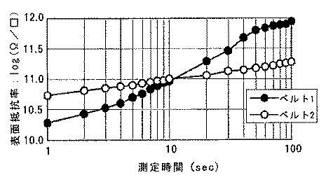
例えば、高抵抗の表層を有する積層ベルトであるベルト1とベルト2との表面抵抗を測定すると、図6に示すように、表面抵抗率の10[sec]値は同等であるが、表面抵抗率の100[sec]値が大きく異なっている。
For example, when the surface resistance of
これは、高抵抗の表層を有する積層ベルトに経時で連続して電圧を印加すると、電圧印加時間に応じて高抵抗の表層と、その表層に隣接する層との界面に電荷が保持され電流が流れにくくなっていき積層ベルトの表面抵抗が上昇していくからである。なお、この上昇量は、表層の抵抗が高くなるほど、上記界面に電荷が保持され易くなるため大きくなることが知られている。 This is because, when a voltage is continuously applied to a laminated belt having a high resistance surface layer over time, electric charges are held at the interface between the high resistance surface layer and a layer adjacent to the surface layer according to the voltage application time, and current flows. This is because it becomes difficult to flow and the surface resistance of the laminated belt increases. It is known that the amount of increase increases as the resistance of the surface layer increases, because charges are more easily held at the interface.
このように表層が高抵抗材料で形成されていれば、表層がたとえ1[μm]の薄層であっても上記界面に電荷が保持されることで発生する残留電荷による残像などの問題が生じ得る。 Thus, if the surface layer is formed of a high-resistance material, even if the surface layer is a thin layer of 1 [μm], problems such as afterimages due to residual charges generated by holding charges at the interface occur. obtain.
そのため、本実験では、表面抵抗率変化量と画像評価との間に関連性が認められるものと考えて、実施例1〜3及び比較例1〜6のベルト部材において、おもて面表面抵抗率変化量と裏面表面抵抗率変化量とを測定した。 Therefore, in this experiment, it is considered that there is a relationship between the surface resistivity change amount and the image evaluation, and in the belt members of Examples 1 to 3 and Comparative Examples 1 to 6, the front surface resistance The rate change amount and the back surface surface resistivity change amount were measured.
なお、表1に示すように裏面表面抵抗率変化量Δρsb100,Δρsb500は、実施例1〜3及び比較例1〜6のいずれのベルト部材も100[V]印加時及び500[V]印加時共に、常用対数値で0.1以下であった。このことから、おもて面の表面抵抗率変化量は表層の抵抗に起因するものであると判断できる。 Incidentally, the back side surface resistivity change amount as shown in Table 1 Δρs b100, Δρs b500 are both in the belt member is also 100 of Examples 1 to 3 and Comparative Examples 1 to 6 [V] is applied at the time and 500 [V] is applied With time, the logarithmic value of common use was 0.1 or less. From this, it can be determined that the surface resistivity change amount of the front surface is caused by the resistance of the surface layer.
また、表1などに基づいて図1に、100[V]印加時のおもて面表面抵抗率変化量Δρsf100を横軸にとり、500[V]印加時のおもて面表面抵抗率変化量Δρsf500を縦軸にとって、実施例1〜3及び比較例1〜6のベルト部材における、おもて面表面抵抗率変化量と画像評価などとの関係を示した。 Further, in FIG. 1 based on Table 1 and the like, the surface surface resistivity change Δρs f100 when 100 [V] is applied is plotted on the horizontal axis, and the surface surface resistivity change when 500 [V] is applied. With the amount Δρs f500 as the vertical axis, the relationship between the surface surface resistivity change amount and image evaluation and the like in the belt members of Examples 1 to 3 and Comparative Examples 1 to 6 is shown.
表1及び図1からわかるように、実施例1〜3のベルト部材においては、画像評価の結果に、許容できないチリ、残像及び放電画像のいずれも発生しておらず、良好な画像が得られた。 As can be seen from Table 1 and FIG. 1, in the belt members of Examples 1 to 3, none of the unacceptable dust, afterimage and discharge image was generated in the image evaluation result, and a good image was obtained. It was.
実施例1〜3のベルト部材においては、印加電圧が低いとき(例えば100[V]印加時)に、経時で連続して電圧を印加することで、ベルト部材のおもて面上に形成されたトナー像を静電的な力によってその場に充分留めることができる程度の量の電荷(トナーの帯電極性とは逆極性の電荷)が表層と中間層との界面などに保持されるため、チリなどの発生を抑制できたと考えられる。また、印加電圧が高いとき(例えば500[V]印加時)には、経時で連続して電圧を印加することで、表層と中間層との界面などにチリや残像などが発生しない程度の量の電荷が保持されるため、チリや残像などの発生を抑制できたと考えられる。 In the belt members of Examples 1 to 3, the belt member is formed on the front surface of the belt member by applying a voltage continuously over time when the applied voltage is low (for example, when 100 [V] is applied). The toner image is held at the interface between the surface layer and the intermediate layer so that the toner image can be held in place by electrostatic force (charge having the opposite polarity to the charged polarity of the toner). It is thought that the occurrence of dust and the like could be suppressed. In addition, when the applied voltage is high (for example, when 500 [V] is applied), the voltage is continuously applied over time so that dust and afterimages do not occur at the interface between the surface layer and the intermediate layer. It is considered that the generation of dust and afterimages could be suppressed because the electric charge was retained.
なお、表1などには示していないが、実施例1〜3のベルト部材においては、大きな表面抵抗率電圧依存性が認められなかった。 In addition, although not shown in Table 1 etc., in the belt members of Examples 1 to 3, large surface resistivity voltage dependency was not recognized.
これに対し、表1及び図1からわかるように、比較例1〜6のベルト部材においては、画像評価の結果に、チリ、残像または放電画像の少なくとも1つが発生した。ここで、比較例2のベルト部材を用いた場合には、チリのランク3.5と評価が「良好」にはならなかったが、許容できる程度のチリであった。また、比較例3のベルト部材及び比較例6のベルト部材を用いた場合には、残像が発生したが許容できる程度であった。よって、比較例1、4及び5のベルト部材を用いた場合には、許容できないチリ、残像または放電画像の少なくとも1つが発生し不良画像となった。また、比較例2のベルト部材を用いた場合には、チリの発生が認められるが実使用上許容できる問題の無い画像が得られた。また、比較例3のベルト部材及び比較例6のベルト部材を用いた場合には、残像の発生が認められるが実使用上許容できる問題の無い画像が得られた。 On the other hand, as can be seen from Table 1 and FIG. 1, in the belt members of Comparative Examples 1 to 6, at least one of dust, an afterimage, or a discharge image occurred as a result of the image evaluation. Here, when the belt member of Comparative Example 2 was used, the dust rank 3.5 and the evaluation did not become “good”, but the dust was acceptable. Further, when the belt member of Comparative Example 3 and the belt member of Comparative Example 6 were used, an afterimage was generated, but it was acceptable. Therefore, when the belt members of Comparative Examples 1, 4, and 5 were used, at least one of unacceptable dust, an afterimage, or a discharge image was generated, resulting in a defective image. Further, when the belt member of Comparative Example 2 was used, generation of dust was observed, but an image having no problem that was acceptable in actual use was obtained. Further, when the belt member of Comparative Example 3 and the belt member of Comparative Example 6 were used, an afterimage was observed, but an image having no acceptable problem in actual use was obtained.
これらの結果から、画像形成装置に用いられる、トナー像を担持する高抵抗の表層を有した多層構造のループ状のベルト部材である中間転写ベルト201として、ループ内側の面である裏面における表面抵抗率の500[V]印加時の10[sec]値が常用対数値[log(Ω/□)]で9.0〜12.5であり、ループ外側の面であるおもて面における表面抵抗率の100[sec]値と1[sec]値との差であるおもて面表面抵抗率変化量が、100[V]印加時に常用対数値[log(Ω/□)]で0.5〜1.50、及び、500[V]印加時に常用対数値[log(Ω/□)]で0.2以下であり、上記裏面における表面抵抗率の100[sec]値と1[sec]値との差である裏面表面抵抗率変化量が、100[V]印加時及び500[V]印加時共に常用対数値[log(Ω/□)]で0.1以下であるベルト部材を用いることで、許容できないチリや残像及び放電画像の発生を抑制することができ、良好な画像が得られることがわかる。
From these results, the
また、少なくともおもて面の表面抵抗率変化量は、印加電圧が低いほど大きくなる傾向にある。例えば、100[V]印加時のおもて面の表面抵抗率変化量Δρsb100が常用対数値[log(Ω/□)]で1.0である、実施例1〜3及び比較例1〜6のベルト部材のような高抵抗の表層を有するベルト部材における500[V]印加時のおもて面の表面抵抗率変化量Δρsb500は、常用対数値[log(Ω/□)]で1.0以上にはならない。このことから、図1に示した灰色部の特性を有するベルト部材は製造できない。 Further, at least the amount of change in the surface resistivity of the front surface tends to increase as the applied voltage decreases. For example, 100 [V] is applied the surface resistivity change amount of the front surface at Derutaroesu b100 is 1.0 common logarithm [log (Ω / □)] , Examples 1 to 3 and Comparative Examples 1 to The surface resistivity change amount Δρs b500 of the belt member having a high resistance surface layer such as the belt member No. 6 when 500 [V] is applied is 1 as a common logarithmic value [log (Ω / □)]. It will not be more than 0. Therefore, the belt member having the gray portion characteristics shown in FIG. 1 cannot be manufactured.
また、本実験で用いたベルト部材は、基層、中間層及び表層が順に積み重なった3層の弾性ベルトであったが、他の構成のベルト部材でも良く、上述した条件を満たすことで、許容できないチリや残像及び放電画像の発生を抑制することができる。 In addition, the belt member used in this experiment was a three-layer elastic belt in which the base layer, the intermediate layer, and the surface layer were sequentially stacked. However, other belt members may be used, and are not acceptable if the above-described conditions are satisfied. Generation of dust, afterimages and discharge images can be suppressed.
以上、本実施形態によれば、画像形成装置に用いられる、トナー像を担持する高抵抗の表層(表面層)を有した多層構造のループ状のベルト部材において、ループ内側の面である裏面における表面抵抗率の500[V]印加時の10[sec]値が常用対数値[log(Ω/□)]で9.0〜12.5であり、ループ外側の面であるおもて面における表面抵抗率の100[sec]値と1[sec]値との差であるおもて面表面抵抗率変化量が、100[V]印加時に常用対数値[log(Ω/□)]で0.5〜1.50、及び、500[V]印加時に常用対数値[log(Ω/□)]で0.2以下であり、上記裏面における表面抵抗率の100[sec]値と1[sec]値との差である裏面表面抵抗率変化量が、100[V]印加時及び500[V]印加時共に常用対数値[log(Ω/□)]で0.1以下であることで、上述した実験で明らかにしたように、許容できないチリや残像及び放電画像の発生を抑制することができ、良好な画像を得ることができる。
また、本実施形態によれば、上述した実験の結果からわかるように、上記表層には少なくともカーボンブラックが添加されていることで、高転写電圧を印加してもチリや残留電荷による残像などの発生を抑制することができる。
また、本実施形態によれば、上述した実験の結果からわかるように、上記おもて面側及び上記裏面側に、電子導電性部材とイオン導電性部材とを含む層である上記表層と上記中間層とが設けられていることで、高転写電圧を印加してもチリや残留電荷による残像の発生を抑制することができる。
また、本実施形態によれば、潜像担持体である感光体102上のトナー像が一時的に転写される中間転写体である中間転写ベルトを備えた転写装置において、上記中間転写ベルトとして本発明のベルト部材を用いることにより、上述した実験の結果からわかるように、許容できないチリや残像及び放電画像の発生を抑制することができ、良好な画像を得ることができる。
また、本実施形態によれば、潜像を担持する潜像担持体である感光体102と、上記潜像をトナー像に現像する現像手段である現像装置104と、感光体102上のトナー像が一時的に転写される中間転写ベルト201を有する転写手段とを備えた画像形成装置において、上記転写手段として、本発明のベルト部材を中間転写ベルト201として用いた転写装置を用いることで、上述した実験の結果からわかるように、許容できないチリ、残像及び放電画像の発生を抑制することができ、良好な画像を得ることができる。
As described above, according to the present embodiment, in the loop-shaped belt member having a high resistance surface layer (surface layer) for carrying the toner image, which is used in the image forming apparatus, on the back surface which is the inner surface of the loop. The value of 10 [sec] when applying a surface resistivity of 500 [V] is 9.0 to 12.5 in the common logarithmic value [log (Ω / □)], and the surface resistivity is the outer surface of the loop. The front surface resistivity change amount, which is the difference between the 100 [sec] value and the 1 [sec] value of the surface resistivity, is 0 in the common logarithmic value [log (Ω / □)] when 100 [V] is applied. The logarithmic value [log (Ω / □)] of 0.2 to 1.50 and 500 [V] is 0.2 or less, and the surface resistivity on the back surface is 100 [sec] and 1 [sec]. ] When the back surface resistivity change amount, which is a difference from the value, is 100 [V] applied, and 5 The common logarithmic value [log (Ω / □)] is 0.1 or less when 0 [V] is applied, thereby suppressing the generation of unacceptable dust, afterimages, and discharge images, as revealed by the above-described experiment. And a good image can be obtained.
In addition, according to the present embodiment, as can be seen from the results of the above-described experiment, at least carbon black is added to the surface layer, so that even if a high transfer voltage is applied, dust and afterimages due to residual charges, etc. Occurrence can be suppressed.
Further, according to the present embodiment, as can be seen from the results of the above-described experiment, the surface layer, which is a layer including an electron conductive member and an ion conductive member, on the front surface side and the back surface side, and the above By providing the intermediate layer, generation of afterimages due to dust and residual charges can be suppressed even when a high transfer voltage is applied.
Further, according to the present embodiment, in the transfer apparatus including the intermediate transfer belt that is an intermediate transfer body to which the toner image on the photosensitive member 102 that is the latent image carrier is temporarily transferred, the intermediate transfer belt is used as the intermediate transfer belt. By using the belt member of the invention, as can be seen from the results of the above-described experiment, generation of unacceptable dust, afterimages and discharge images can be suppressed, and a good image can be obtained.
Further, according to the present embodiment, the photosensitive member 102 that is a latent image carrier that carries a latent image, the developing device 104 that is a developing unit that develops the latent image into a toner image, and the toner image on the photosensitive member 102. In the image forming apparatus including the transfer unit having the
101 画像形成部
102 感光体
104 現像装置
200 転写装置
201 中間転写ベルト
DESCRIPTION OF SYMBOLS 101 Image forming part 102 Photoconductor 104
Claims (5)
ループ内側の面である裏面における表面抵抗率の500[V]印加時の10[sec]測定値が常用対数値[log(Ω/□)]で9.0〜12.5であり、
ループ外側の面であるおもて面における表面抵抗率の100[sec]測定値と1[sec]測定値との差であるおもて面表面抵抗率変化量が、100[V]印加時に常用対数値[log(Ω/□)]で0.5〜1.50、及び、500[V]印加時に常用対数値[log(Ω/□)]で0.2以下であり、
該裏面における表面抵抗率の100[sec]測定値と1[sec]測定値との差である裏面表面抵抗率変化量が、100[V]印加時及び500[V]印加時共に常用対数値[log(Ω/□)]で0.1以下であることを特徴とするベルト部材。 In a loop-shaped belt member having a multi-layer structure having a high-resistance surface layer for supporting a toner image used in an image forming apparatus,
10 [sec] measured value at the time of 500 [V] application of the surface resistivity on the back surface which is the inner surface of the loop is 9.0 to 12.5 in the common logarithmic value [log (Ω / □)],
When the surface resistivity change of the front surface, which is the difference between the measured value of 100 [sec] and the measured value of 1 [sec] on the front surface, which is the outer surface of the loop, is 100 [V] applied. The common logarithmic value [log (Ω / □)] is 0.5 to 1.50, and the common logarithmic value [log (Ω / □)] is 0.2 or less when 500 [V] is applied,
The back surface resistivity change amount, which is the difference between the measured value of 100 [sec] and 1 [sec] of the surface resistivity on the back surface, is a common logarithm when both 100 [V] and 500 [V] are applied. A belt member, wherein [log (Ω / □)] is 0.1 or less.
上記表面層には少なくともカーボンブラックが添加されていることを特徴とするベルト部材。 The belt member according to claim 1, wherein
A belt member, wherein at least carbon black is added to the surface layer.
上記おもて面側及び上記裏面側に、電子導電性部材とイオン導電性部材とを含む層が設けられていることを特徴とするベルト部材。 The belt member according to claim 1 or 2,
A belt member comprising a layer including an electronic conductive member and an ion conductive member on the front surface side and the back surface side.
該中間転写体として、請求項1、2または3のベルト部材を用いることを特徴とする転写装置。 In a transfer device including an intermediate transfer body to which a toner image on a latent image carrier is temporarily transferred,
A transfer device using the belt member according to claim 1, 2 or 3 as the intermediate transfer member.
該潜像をトナー像に現像する現像手段と、
該潜像担持体上のトナー像が一時的に転写される中間転写ベルトを有する転写手段とを備えた画像形成装置において、
該転写手段として、請求項4の転写装置を用いることを特徴とする画像形成装置。 A latent image carrier for carrying a latent image;
Developing means for developing the latent image into a toner image;
An image forming apparatus comprising a transfer unit having an intermediate transfer belt to which a toner image on the latent image carrier is temporarily transferred;
An image forming apparatus using the transfer device according to claim 4 as the transfer means.
Priority Applications (4)
| Application Number | Priority Date | Filing Date | Title |
|---|---|---|---|
| JP2008190787A JP5142037B2 (en) | 2008-07-24 | 2008-07-24 | Belt member, transfer device, and image forming apparatus |
| EP09166103A EP2148249A3 (en) | 2008-07-24 | 2009-07-22 | Endless belt member, transfer unit incorporating same, and image forming apparatus incorporating same |
| CN2009101651812A CN101634828B (en) | 2008-07-24 | 2009-07-23 | Belt member, transfer unit and image forming apparatus |
| US12/508,255 US7953355B2 (en) | 2008-07-24 | 2009-07-23 | Endless belt member, transfer unit incorporating same, and image forming apparatus incorporating same |
Applications Claiming Priority (1)
| Application Number | Priority Date | Filing Date | Title |
|---|---|---|---|
| JP2008190787A JP5142037B2 (en) | 2008-07-24 | 2008-07-24 | Belt member, transfer device, and image forming apparatus |
Publications (2)
| Publication Number | Publication Date |
|---|---|
| JP2010026432A JP2010026432A (en) | 2010-02-04 |
| JP5142037B2 true JP5142037B2 (en) | 2013-02-13 |
Family
ID=40983515
Family Applications (1)
| Application Number | Title | Priority Date | Filing Date |
|---|---|---|---|
| JP2008190787A Expired - Fee Related JP5142037B2 (en) | 2008-07-24 | 2008-07-24 | Belt member, transfer device, and image forming apparatus |
Country Status (4)
| Country | Link |
|---|---|
| US (1) | US7953355B2 (en) |
| EP (1) | EP2148249A3 (en) |
| JP (1) | JP5142037B2 (en) |
| CN (1) | CN101634828B (en) |
Cited By (1)
| Publication number | Priority date | Publication date | Assignee | Title |
|---|---|---|---|---|
| US9316957B2 (en) | 2013-05-15 | 2016-04-19 | Fuji Xerox Co., Ltd. | Transfer device and image forming apparatus |
Families Citing this family (11)
| Publication number | Priority date | Publication date | Assignee | Title |
|---|---|---|---|---|
| US8929785B1 (en) | 2011-02-01 | 2015-01-06 | Xerox Corporation | Endless flexible members for imaging devices |
| US8543043B2 (en) * | 2011-02-01 | 2013-09-24 | Xerox Corporation | Endless flexible members for imaging devices |
| CN102650735B (en) * | 2011-02-28 | 2014-08-27 | 株式会社理光 | Method for irradiating photoreceptor by using laser and image forming device |
| JP4844700B1 (en) * | 2011-08-16 | 2011-12-28 | 富士ゼロックス株式会社 | Manufacturing method of endless belt |
| JP2014122958A (en) * | 2012-12-20 | 2014-07-03 | Canon Inc | Image forming apparatus |
| US20150314461A1 (en) * | 2014-05-02 | 2015-11-05 | Raymond Industrial Ltd. | Hybrid Shaving System |
| JP2016006467A (en) * | 2014-06-20 | 2016-01-14 | 株式会社リコー | Method of manufacturing intermediate transfer belt, intermediate transfer belt, and image formation device |
| JP6128108B2 (en) * | 2014-12-11 | 2017-05-17 | コニカミノルタ株式会社 | Intermediate transfer belt and image forming apparatus |
| US10647134B2 (en) * | 2018-02-23 | 2020-05-12 | Kabushiki Kaisha Toshiba | Transfer belt platens |
| JP2020194002A (en) | 2019-05-24 | 2020-12-03 | 富士ゼロックス株式会社 | Belt, intermediate transfer belt, and image forming apparatus |
| JP7367500B2 (en) * | 2019-12-06 | 2023-10-24 | 富士フイルムビジネスイノベーション株式会社 | Transfer unit, transfer device, and image forming device |
Family Cites Families (31)
| Publication number | Priority date | Publication date | Assignee | Title |
|---|---|---|---|---|
| KR100324101B1 (en) * | 1998-02-14 | 2002-02-20 | 이토가 미찌야 | Image forming apparatus |
| JPH11282277A (en) | 1998-03-30 | 1999-10-15 | Ricoh Co Ltd | Image forming method and image forming device |
| JP4038328B2 (en) | 1999-10-29 | 2008-01-23 | 株式会社リコー | Image forming apparatus, transfer material conveying method, and transfer apparatus |
| JP3859112B2 (en) | 2000-02-28 | 2006-12-20 | 株式会社リコー | Image forming apparatus |
| JP3963638B2 (en) | 2000-09-07 | 2007-08-22 | 株式会社リコー | Image forming apparatus |
| US6611672B2 (en) | 2000-09-26 | 2003-08-26 | Ricoh Company, Ltd. | Image forming apparatus, monocolor image forming apparatus, toner recycling apparatus and intermediate transfer member |
| EP1351100B1 (en) * | 2001-01-12 | 2012-07-25 | Fuji Xerox Co., Ltd. | Color image forming device |
| JP2003029550A (en) | 2001-07-13 | 2003-01-31 | Ricoh Co Ltd | Image forming device |
| JP2003029541A (en) | 2001-07-13 | 2003-01-31 | Ricoh Co Ltd | Image forming device |
| JP4004020B2 (en) | 2001-07-23 | 2007-11-07 | 株式会社リコー | Bias application method, bias application device, and image forming apparatus |
| JP2003131497A (en) | 2001-10-29 | 2003-05-09 | Ricoh Co Ltd | Tranfer device and image forming device using the same |
| JP2003255769A (en) | 2002-02-28 | 2003-09-10 | Ricoh Co Ltd | Image forming apparatus |
| JP3972694B2 (en) | 2002-03-15 | 2007-09-05 | 富士ゼロックス株式会社 | Conductive member and image forming apparatus using the same |
| US6901234B2 (en) * | 2002-03-18 | 2005-05-31 | Ricoh Company, Ltd. | Image forming apparatus including an intermediate image transfer belt and high resistance contact member |
| US7174124B2 (en) | 2002-09-13 | 2007-02-06 | Ricoh Company, Ltd. | Tandem color image forming apparatus with an image transfer belt and backup roller |
| EP1424608B1 (en) | 2002-11-05 | 2015-07-22 | Ricoh Company, Ltd. | Colour image forming apparatus |
| JP2004184875A (en) * | 2002-12-05 | 2004-07-02 | Ricoh Co Ltd | Transfer device and image forming apparatus |
| JP2004287383A (en) * | 2003-03-06 | 2004-10-14 | Fuji Xerox Co Ltd | Semiconductive belt and image forming apparatus using the same |
| JP4778671B2 (en) * | 2003-07-02 | 2011-09-21 | 株式会社リコー | Method for determining resistance change of transfer member used in image forming apparatus |
| JP4294546B2 (en) | 2004-06-25 | 2009-07-15 | 株式会社リコー | Belt member, and belt driving apparatus and image forming apparatus using the same |
| JP2006030528A (en) * | 2004-07-15 | 2006-02-02 | Oki Data Corp | Endless belt carrier and image forming apparatus |
| US7292813B2 (en) * | 2004-08-31 | 2007-11-06 | Fuji Xerox Co., Ltd. | Intermediate transfer belt, production method for the same, and image forming device provided with the same |
| JP2006106667A (en) | 2004-09-10 | 2006-04-20 | Ricoh Co Ltd | Transfer device and image forming apparatus |
| US7502583B2 (en) * | 2004-09-10 | 2009-03-10 | Ricoh Company, Limited | Transfer device and image forming apparatus for enhancement of an image stored on a recording medium |
| CN100589043C (en) * | 2005-12-08 | 2010-02-10 | 株式会社理光 | An image forming apparatus capable of preventing generation of residual image and transfer failure |
| JP5081428B2 (en) | 2005-12-08 | 2012-11-28 | 株式会社リコー | Image forming apparatus |
| JP4724601B2 (en) | 2006-05-16 | 2011-07-13 | 株式会社リコー | Image forming apparatus and image forming method |
| JP2007316230A (en) * | 2006-05-24 | 2007-12-06 | Canon Chemicals Inc | Polyurethane foam roller and toner supply roller |
| JP5095133B2 (en) | 2006-06-06 | 2012-12-12 | 株式会社リコー | Method for manufacturing transfer device |
| JP2007328198A (en) | 2006-06-08 | 2007-12-20 | Ricoh Co Ltd | Image forming apparatus |
| JP2009139657A (en) | 2007-12-06 | 2009-06-25 | Ricoh Co Ltd | Belt member, transfer unit, image forming apparatus, and evaluation method for determining belt member specification |
-
2008
- 2008-07-24 JP JP2008190787A patent/JP5142037B2/en not_active Expired - Fee Related
-
2009
- 2009-07-22 EP EP09166103A patent/EP2148249A3/en not_active Withdrawn
- 2009-07-23 US US12/508,255 patent/US7953355B2/en not_active Expired - Fee Related
- 2009-07-23 CN CN2009101651812A patent/CN101634828B/en active Active
Cited By (1)
| Publication number | Priority date | Publication date | Assignee | Title |
|---|---|---|---|---|
| US9316957B2 (en) | 2013-05-15 | 2016-04-19 | Fuji Xerox Co., Ltd. | Transfer device and image forming apparatus |
Also Published As
| Publication number | Publication date |
|---|---|
| US20100021216A1 (en) | 2010-01-28 |
| EP2148249A2 (en) | 2010-01-27 |
| CN101634828B (en) | 2012-01-11 |
| CN101634828A (en) | 2010-01-27 |
| JP2010026432A (en) | 2010-02-04 |
| US7953355B2 (en) | 2011-05-31 |
| EP2148249A3 (en) | 2011-03-16 |
Similar Documents
| Publication | Publication Date | Title |
|---|---|---|
| JP5142037B2 (en) | Belt member, transfer device, and image forming apparatus | |
| JP2009139657A (en) | Belt member, transfer unit, image forming apparatus, and evaluation method for determining belt member specification | |
| JP3248455B2 (en) | Image forming apparatus and method of manufacturing intermediate transfer belt used in the same | |
| JP5429419B2 (en) | Annular body, annular body unit and image forming apparatus | |
| JPH1083122A (en) | Image forming device, intermediate transferring body belt and their production | |
| US20170242372A1 (en) | Tubular member, transfer belt, transfer unit, and image forming apparatus | |
| JP2018155953A (en) | Intermediate transfer body and image forming apparatus | |
| JP5866778B2 (en) | Method for producing cylindrical molded body | |
| JP5579655B2 (en) | Image forming apparatus | |
| JP5470771B2 (en) | Image forming apparatus | |
| US8543031B2 (en) | Intermediate transfer member reconditioning | |
| US20170242373A1 (en) | Tubular member, transfer belt, transfer unit, and image forming apparatus | |
| JP2019200318A (en) | Belt, endless belt, intermediate transfer belt and image formation device | |
| JP4477219B2 (en) | Intermediate transfer body manufacturing method, intermediate transfer body, and image forming apparatus | |
| JP2000330390A (en) | Image forming device | |
| JP6056542B2 (en) | Tubular body, tubular body unit, intermediate transfer body, and image forming apparatus | |
| JP2009258698A (en) | Circular body, circular body unit, and image forming apparatus | |
| JP4127179B2 (en) | Semi-conductive seamless belt | |
| JP2007316272A (en) | Intermediate transfer body and image forming method | |
| JP2009258708A (en) | Circular body, circular body unit, and image forming apparatus | |
| US20240094663A1 (en) | Transfer device and image forming apparatus | |
| JP2018084661A (en) | Endless belt, endless belt unit, and image forming apparatus | |
| JP6743639B2 (en) | Intermediate transfer belt, transfer unit, and image forming apparatus | |
| JP2010060811A (en) | Image forming apparatus | |
| JP6232922B2 (en) | Tubular body, tubular body unit, intermediate transfer body, image forming apparatus, and process cartridge |
Legal Events
| Date | Code | Title | Description |
|---|---|---|---|
| A621 | Written request for application examination |
Free format text: JAPANESE INTERMEDIATE CODE: A621 Effective date: 20110324 |
|
| TRDD | Decision of grant or rejection written | ||
| A977 | Report on retrieval |
Free format text: JAPANESE INTERMEDIATE CODE: A971007 Effective date: 20121024 |
|
| A01 | Written decision to grant a patent or to grant a registration (utility model) |
Free format text: JAPANESE INTERMEDIATE CODE: A01 Effective date: 20121026 |
|
| A01 | Written decision to grant a patent or to grant a registration (utility model) |
Free format text: JAPANESE INTERMEDIATE CODE: A01 |
|
| A61 | First payment of annual fees (during grant procedure) |
Free format text: JAPANESE INTERMEDIATE CODE: A61 Effective date: 20121108 |
|
| FPAY | Renewal fee payment (event date is renewal date of database) |
Free format text: PAYMENT UNTIL: 20151130 Year of fee payment: 3 |
|
| R151 | Written notification of patent or utility model registration |
Ref document number: 5142037 Country of ref document: JP Free format text: JAPANESE INTERMEDIATE CODE: R151 |
|
| LAPS | Cancellation because of no payment of annual fees |