JP5106460B2 - 半導体装置及びその製造方法、並びに電子装置 - Google Patents
半導体装置及びその製造方法、並びに電子装置 Download PDFInfo
- Publication number
- JP5106460B2 JP5106460B2 JP2009077033A JP2009077033A JP5106460B2 JP 5106460 B2 JP5106460 B2 JP 5106460B2 JP 2009077033 A JP2009077033 A JP 2009077033A JP 2009077033 A JP2009077033 A JP 2009077033A JP 5106460 B2 JP5106460 B2 JP 5106460B2
- Authority
- JP
- Japan
- Prior art keywords
- semiconductor device
- electrode
- pad
- electronic component
- electrode pad
- Prior art date
- Legal status (The legal status is an assumption and is not a legal conclusion. Google has not performed a legal analysis and makes no representation as to the accuracy of the status listed.)
- Active
Links
- 239000004065 semiconductor Substances 0.000 title claims abstract description 267
- 238000004519 manufacturing process Methods 0.000 title claims description 29
- 239000011347 resin Substances 0.000 claims abstract description 126
- 229920005989 resin Polymers 0.000 claims abstract description 126
- 239000004020 conductor Substances 0.000 claims abstract description 14
- 238000007789 sealing Methods 0.000 claims description 92
- 239000000758 substrate Substances 0.000 claims description 65
- 239000000853 adhesive Substances 0.000 claims description 39
- 229910000679 solder Inorganic materials 0.000 claims description 37
- 230000001070 adhesive effect Effects 0.000 claims description 36
- XUIMIQQOPSSXEZ-UHFFFAOYSA-N Silicon Chemical compound [Si] XUIMIQQOPSSXEZ-UHFFFAOYSA-N 0.000 claims description 30
- 229910052710 silicon Inorganic materials 0.000 claims description 30
- 239000010703 silicon Substances 0.000 claims description 30
- 230000000149 penetrating effect Effects 0.000 claims description 29
- 238000000034 method Methods 0.000 claims description 28
- 238000003780 insertion Methods 0.000 claims description 5
- 230000037431 insertion Effects 0.000 claims description 5
- 230000007261 regionalization Effects 0.000 claims description 2
- 239000000463 material Substances 0.000 description 20
- 238000012986 modification Methods 0.000 description 20
- 230000004048 modification Effects 0.000 description 20
- 239000002184 metal Substances 0.000 description 11
- 230000015572 biosynthetic process Effects 0.000 description 9
- 230000035515 penetration Effects 0.000 description 9
- 230000000694 effects Effects 0.000 description 8
- 239000004593 Epoxy Substances 0.000 description 6
- 238000005498 polishing Methods 0.000 description 6
- 238000010586 diagram Methods 0.000 description 4
- 239000003822 epoxy resin Substances 0.000 description 4
- 229920000647 polyepoxide Polymers 0.000 description 4
- 229910004298 SiO 2 Inorganic materials 0.000 description 2
- BZHJMEDXRYGGRV-UHFFFAOYSA-N Vinyl chloride Chemical compound ClC=C BZHJMEDXRYGGRV-UHFFFAOYSA-N 0.000 description 2
- 239000004927 clay Substances 0.000 description 2
- 150000001875 compounds Chemical class 0.000 description 2
- -1 epoxy Chemical class 0.000 description 2
- 239000011521 glass Substances 0.000 description 2
- 238000010438 heat treatment Methods 0.000 description 2
- 238000007747 plating Methods 0.000 description 2
- 238000004080 punching Methods 0.000 description 2
- 239000000654 additive Substances 0.000 description 1
- 239000003795 chemical substances by application Substances 0.000 description 1
- 238000005229 chemical vapour deposition Methods 0.000 description 1
- 238000005553 drilling Methods 0.000 description 1
- 238000005530 etching Methods 0.000 description 1
- 230000006870 function Effects 0.000 description 1
- 238000010030 laminating Methods 0.000 description 1
- 230000003647 oxidation Effects 0.000 description 1
- 238000007254 oxidation reaction Methods 0.000 description 1
- 238000001020 plasma etching Methods 0.000 description 1
- 238000004382 potting Methods 0.000 description 1
- 238000003825 pressing Methods 0.000 description 1
- 239000000126 substance Substances 0.000 description 1
- 238000001721 transfer moulding Methods 0.000 description 1
- 238000001039 wet etching Methods 0.000 description 1
Images


Classifications
-
- H—ELECTRICITY
- H01—ELECTRIC ELEMENTS
- H01L—SEMICONDUCTOR DEVICES NOT COVERED BY CLASS H10
- H01L23/00—Details of semiconductor or other solid state devices
- H01L23/48—Arrangements for conducting electric current to or from the solid state body in operation, e.g. leads, terminal arrangements ; Selection of materials therefor
- H01L23/488—Arrangements for conducting electric current to or from the solid state body in operation, e.g. leads, terminal arrangements ; Selection of materials therefor consisting of soldered or bonded constructions
- H01L23/498—Leads, i.e. metallisations or lead-frames on insulating substrates, e.g. chip carriers
- H01L23/49827—Via connections through the substrates, e.g. pins going through the substrate, coaxial cables
-
- H—ELECTRICITY
- H01—ELECTRIC ELEMENTS
- H01L—SEMICONDUCTOR DEVICES NOT COVERED BY CLASS H10
- H01L21/00—Processes or apparatus adapted for the manufacture or treatment of semiconductor or solid state devices or of parts thereof
- H01L21/67—Apparatus specially adapted for handling semiconductor or electric solid state devices during manufacture or treatment thereof; Apparatus specially adapted for handling wafers during manufacture or treatment of semiconductor or electric solid state devices or components ; Apparatus not specifically provided for elsewhere
- H01L21/683—Apparatus specially adapted for handling semiconductor or electric solid state devices during manufacture or treatment thereof; Apparatus specially adapted for handling wafers during manufacture or treatment of semiconductor or electric solid state devices or components ; Apparatus not specifically provided for elsewhere for supporting or gripping
- H01L21/6835—Apparatus specially adapted for handling semiconductor or electric solid state devices during manufacture or treatment thereof; Apparatus specially adapted for handling wafers during manufacture or treatment of semiconductor or electric solid state devices or components ; Apparatus not specifically provided for elsewhere for supporting or gripping using temporarily an auxiliary support
-
- H—ELECTRICITY
- H01—ELECTRIC ELEMENTS
- H01L—SEMICONDUCTOR DEVICES NOT COVERED BY CLASS H10
- H01L23/00—Details of semiconductor or other solid state devices
- H01L23/12—Mountings, e.g. non-detachable insulating substrates
- H01L23/13—Mountings, e.g. non-detachable insulating substrates characterised by the shape
-
- H—ELECTRICITY
- H01—ELECTRIC ELEMENTS
- H01L—SEMICONDUCTOR DEVICES NOT COVERED BY CLASS H10
- H01L23/00—Details of semiconductor or other solid state devices
- H01L23/48—Arrangements for conducting electric current to or from the solid state body in operation, e.g. leads, terminal arrangements ; Selection of materials therefor
- H01L23/488—Arrangements for conducting electric current to or from the solid state body in operation, e.g. leads, terminal arrangements ; Selection of materials therefor consisting of soldered or bonded constructions
- H01L23/498—Leads, i.e. metallisations or lead-frames on insulating substrates, e.g. chip carriers
- H01L23/49811—Additional leads joined to the metallisation on the insulating substrate, e.g. pins, bumps, wires, flat leads
- H01L23/49816—Spherical bumps on the substrate for external connection, e.g. ball grid arrays [BGA]
-
- H—ELECTRICITY
- H01—ELECTRIC ELEMENTS
- H01L—SEMICONDUCTOR DEVICES NOT COVERED BY CLASS H10
- H01L23/00—Details of semiconductor or other solid state devices
- H01L23/52—Arrangements for conducting electric current within the device in operation from one component to another, i.e. interconnections, e.g. wires, lead frames
- H01L23/538—Arrangements for conducting electric current within the device in operation from one component to another, i.e. interconnections, e.g. wires, lead frames the interconnection structure between a plurality of semiconductor chips being formed on, or in, insulating substrates
- H01L23/5389—Arrangements for conducting electric current within the device in operation from one component to another, i.e. interconnections, e.g. wires, lead frames the interconnection structure between a plurality of semiconductor chips being formed on, or in, insulating substrates the chips being integrally enclosed by the interconnect and support structures
-
- H—ELECTRICITY
- H01—ELECTRIC ELEMENTS
- H01L—SEMICONDUCTOR DEVICES NOT COVERED BY CLASS H10
- H01L24/00—Arrangements for connecting or disconnecting semiconductor or solid-state bodies; Methods or apparatus related thereto
- H01L24/01—Means for bonding being attached to, or being formed on, the surface to be connected, e.g. chip-to-package, die-attach, "first-level" interconnects; Manufacturing methods related thereto
- H01L24/18—High density interconnect [HDI] connectors; Manufacturing methods related thereto
- H01L24/19—Manufacturing methods of high density interconnect preforms
-
- H—ELECTRICITY
- H01—ELECTRIC ELEMENTS
- H01L—SEMICONDUCTOR DEVICES NOT COVERED BY CLASS H10
- H01L24/00—Arrangements for connecting or disconnecting semiconductor or solid-state bodies; Methods or apparatus related thereto
- H01L24/80—Methods for connecting semiconductor or other solid state bodies using means for bonding being attached to, or being formed on, the surface to be connected
- H01L24/82—Methods for connecting semiconductor or other solid state bodies using means for bonding being attached to, or being formed on, the surface to be connected by forming build-up interconnects at chip-level, e.g. for high density interconnects [HDI]
-
- H—ELECTRICITY
- H01—ELECTRIC ELEMENTS
- H01L—SEMICONDUCTOR DEVICES NOT COVERED BY CLASS H10
- H01L25/00—Assemblies consisting of a plurality of semiconductor or other solid state devices
- H01L25/03—Assemblies consisting of a plurality of semiconductor or other solid state devices all the devices being of a type provided for in a single subclass of subclasses H10B, H10F, H10H, H10K or H10N, e.g. assemblies of rectifier diodes
- H01L25/10—Assemblies consisting of a plurality of semiconductor or other solid state devices all the devices being of a type provided for in a single subclass of subclasses H10B, H10F, H10H, H10K or H10N, e.g. assemblies of rectifier diodes the devices having separate containers
- H01L25/105—Assemblies consisting of a plurality of semiconductor or other solid state devices all the devices being of a type provided for in a single subclass of subclasses H10B, H10F, H10H, H10K or H10N, e.g. assemblies of rectifier diodes the devices having separate containers the devices being integrated devices of class H10
-
- H—ELECTRICITY
- H01—ELECTRIC ELEMENTS
- H01L—SEMICONDUCTOR DEVICES NOT COVERED BY CLASS H10
- H01L21/00—Processes or apparatus adapted for the manufacture or treatment of semiconductor or solid state devices or of parts thereof
- H01L21/02—Manufacture or treatment of semiconductor devices or of parts thereof
- H01L21/04—Manufacture or treatment of semiconductor devices or of parts thereof the devices having potential barriers, e.g. a PN junction, depletion layer or carrier concentration layer
- H01L21/50—Assembly of semiconductor devices using processes or apparatus not provided for in a single one of the groups H01L21/18 - H01L21/326 or H10D48/04 - H10D48/07 e.g. sealing of a cap to a base of a container
- H01L21/56—Encapsulations, e.g. encapsulation layers, coatings
- H01L21/568—Temporary substrate used as encapsulation process aid
-
- H—ELECTRICITY
- H01—ELECTRIC ELEMENTS
- H01L—SEMICONDUCTOR DEVICES NOT COVERED BY CLASS H10
- H01L2221/00—Processes or apparatus adapted for the manufacture or treatment of semiconductor or solid state devices or of parts thereof covered by H01L21/00
- H01L2221/67—Apparatus for handling semiconductor or electric solid state devices during manufacture or treatment thereof; Apparatus for handling wafers during manufacture or treatment of semiconductor or electric solid state devices or components; Apparatus not specifically provided for elsewhere
- H01L2221/683—Apparatus for handling semiconductor or electric solid state devices during manufacture or treatment thereof; Apparatus for handling wafers during manufacture or treatment of semiconductor or electric solid state devices or components; Apparatus not specifically provided for elsewhere for supporting or gripping
- H01L2221/68304—Apparatus for handling semiconductor or electric solid state devices during manufacture or treatment thereof; Apparatus for handling wafers during manufacture or treatment of semiconductor or electric solid state devices or components; Apparatus not specifically provided for elsewhere for supporting or gripping using temporarily an auxiliary support
- H01L2221/68345—Apparatus for handling semiconductor or electric solid state devices during manufacture or treatment thereof; Apparatus for handling wafers during manufacture or treatment of semiconductor or electric solid state devices or components; Apparatus not specifically provided for elsewhere for supporting or gripping using temporarily an auxiliary support used as a support during the manufacture of self supporting substrates
-
- H—ELECTRICITY
- H01—ELECTRIC ELEMENTS
- H01L—SEMICONDUCTOR DEVICES NOT COVERED BY CLASS H10
- H01L2224/00—Indexing scheme for arrangements for connecting or disconnecting semiconductor or solid-state bodies and methods related thereto as covered by H01L24/00
- H01L2224/01—Means for bonding being attached to, or being formed on, the surface to be connected, e.g. chip-to-package, die-attach, "first-level" interconnects; Manufacturing methods related thereto
- H01L2224/02—Bonding areas; Manufacturing methods related thereto
- H01L2224/04—Structure, shape, material or disposition of the bonding areas prior to the connecting process
- H01L2224/0401—Bonding areas specifically adapted for bump connectors, e.g. under bump metallisation [UBM]
-
- H—ELECTRICITY
- H01—ELECTRIC ELEMENTS
- H01L—SEMICONDUCTOR DEVICES NOT COVERED BY CLASS H10
- H01L2224/00—Indexing scheme for arrangements for connecting or disconnecting semiconductor or solid-state bodies and methods related thereto as covered by H01L24/00
- H01L2224/01—Means for bonding being attached to, or being formed on, the surface to be connected, e.g. chip-to-package, die-attach, "first-level" interconnects; Manufacturing methods related thereto
- H01L2224/02—Bonding areas; Manufacturing methods related thereto
- H01L2224/04—Structure, shape, material or disposition of the bonding areas prior to the connecting process
- H01L2224/04105—Bonding areas formed on an encapsulation of the semiconductor or solid-state body, e.g. bonding areas on chip-scale packages
-
- H—ELECTRICITY
- H01—ELECTRIC ELEMENTS
- H01L—SEMICONDUCTOR DEVICES NOT COVERED BY CLASS H10
- H01L2224/00—Indexing scheme for arrangements for connecting or disconnecting semiconductor or solid-state bodies and methods related thereto as covered by H01L24/00
- H01L2224/01—Means for bonding being attached to, or being formed on, the surface to be connected, e.g. chip-to-package, die-attach, "first-level" interconnects; Manufacturing methods related thereto
- H01L2224/02—Bonding areas; Manufacturing methods related thereto
- H01L2224/04—Structure, shape, material or disposition of the bonding areas prior to the connecting process
- H01L2224/05—Structure, shape, material or disposition of the bonding areas prior to the connecting process of an individual bonding area
- H01L2224/05001—Internal layers
- H01L2224/05099—Material
- H01L2224/051—Material with a principal constituent of the material being a metal or a metalloid, e.g. boron [B], silicon [Si], germanium [Ge], arsenic [As], antimony [Sb], tellurium [Te] and polonium [Po], and alloys thereof
- H01L2224/05138—Material with a principal constituent of the material being a metal or a metalloid, e.g. boron [B], silicon [Si], germanium [Ge], arsenic [As], antimony [Sb], tellurium [Te] and polonium [Po], and alloys thereof the principal constituent melting at a temperature of greater than or equal to 950°C and less than 1550°C
- H01L2224/05147—Copper [Cu] as principal constituent
-
- H—ELECTRICITY
- H01—ELECTRIC ELEMENTS
- H01L—SEMICONDUCTOR DEVICES NOT COVERED BY CLASS H10
- H01L2224/00—Indexing scheme for arrangements for connecting or disconnecting semiconductor or solid-state bodies and methods related thereto as covered by H01L24/00
- H01L2224/01—Means for bonding being attached to, or being formed on, the surface to be connected, e.g. chip-to-package, die-attach, "first-level" interconnects; Manufacturing methods related thereto
- H01L2224/10—Bump connectors; Manufacturing methods related thereto
- H01L2224/12—Structure, shape, material or disposition of the bump connectors prior to the connecting process
- H01L2224/12105—Bump connectors formed on an encapsulation of the semiconductor or solid-state body, e.g. bumps on chip-scale packages
-
- H—ELECTRICITY
- H01—ELECTRIC ELEMENTS
- H01L—SEMICONDUCTOR DEVICES NOT COVERED BY CLASS H10
- H01L2224/00—Indexing scheme for arrangements for connecting or disconnecting semiconductor or solid-state bodies and methods related thereto as covered by H01L24/00
- H01L2224/01—Means for bonding being attached to, or being formed on, the surface to be connected, e.g. chip-to-package, die-attach, "first-level" interconnects; Manufacturing methods related thereto
- H01L2224/10—Bump connectors; Manufacturing methods related thereto
- H01L2224/15—Structure, shape, material or disposition of the bump connectors after the connecting process
- H01L2224/16—Structure, shape, material or disposition of the bump connectors after the connecting process of an individual bump connector
- H01L2224/161—Disposition
- H01L2224/16151—Disposition the bump connector connecting between a semiconductor or solid-state body and an item not being a semiconductor or solid-state body, e.g. chip-to-substrate, chip-to-passive
- H01L2224/16221—Disposition the bump connector connecting between a semiconductor or solid-state body and an item not being a semiconductor or solid-state body, e.g. chip-to-substrate, chip-to-passive the body and the item being stacked
- H01L2224/16225—Disposition the bump connector connecting between a semiconductor or solid-state body and an item not being a semiconductor or solid-state body, e.g. chip-to-substrate, chip-to-passive the body and the item being stacked the item being non-metallic, e.g. insulating substrate with or without metallisation
- H01L2224/16227—Disposition the bump connector connecting between a semiconductor or solid-state body and an item not being a semiconductor or solid-state body, e.g. chip-to-substrate, chip-to-passive the body and the item being stacked the item being non-metallic, e.g. insulating substrate with or without metallisation the bump connector connecting to a bond pad of the item
-
- H—ELECTRICITY
- H01—ELECTRIC ELEMENTS
- H01L—SEMICONDUCTOR DEVICES NOT COVERED BY CLASS H10
- H01L2224/00—Indexing scheme for arrangements for connecting or disconnecting semiconductor or solid-state bodies and methods related thereto as covered by H01L24/00
- H01L2224/01—Means for bonding being attached to, or being formed on, the surface to be connected, e.g. chip-to-package, die-attach, "first-level" interconnects; Manufacturing methods related thereto
- H01L2224/26—Layer connectors, e.g. plate connectors, solder or adhesive layers; Manufacturing methods related thereto
- H01L2224/31—Structure, shape, material or disposition of the layer connectors after the connecting process
- H01L2224/32—Structure, shape, material or disposition of the layer connectors after the connecting process of an individual layer connector
- H01L2224/321—Disposition
- H01L2224/32151—Disposition the layer connector connecting between a semiconductor or solid-state body and an item not being a semiconductor or solid-state body, e.g. chip-to-substrate, chip-to-passive
- H01L2224/32221—Disposition the layer connector connecting between a semiconductor or solid-state body and an item not being a semiconductor or solid-state body, e.g. chip-to-substrate, chip-to-passive the body and the item being stacked
- H01L2224/32225—Disposition the layer connector connecting between a semiconductor or solid-state body and an item not being a semiconductor or solid-state body, e.g. chip-to-substrate, chip-to-passive the body and the item being stacked the item being non-metallic, e.g. insulating substrate with or without metallisation
-
- H—ELECTRICITY
- H01—ELECTRIC ELEMENTS
- H01L—SEMICONDUCTOR DEVICES NOT COVERED BY CLASS H10
- H01L2224/00—Indexing scheme for arrangements for connecting or disconnecting semiconductor or solid-state bodies and methods related thereto as covered by H01L24/00
- H01L2224/01—Means for bonding being attached to, or being formed on, the surface to be connected, e.g. chip-to-package, die-attach, "first-level" interconnects; Manufacturing methods related thereto
- H01L2224/42—Wire connectors; Manufacturing methods related thereto
- H01L2224/44—Structure, shape, material or disposition of the wire connectors prior to the connecting process
- H01L2224/45—Structure, shape, material or disposition of the wire connectors prior to the connecting process of an individual wire connector
- H01L2224/45001—Core members of the connector
- H01L2224/45099—Material
- H01L2224/451—Material with a principal constituent of the material being a metal or a metalloid, e.g. boron (B), silicon (Si), germanium (Ge), arsenic (As), antimony (Sb), tellurium (Te) and polonium (Po), and alloys thereof
- H01L2224/45138—Material with a principal constituent of the material being a metal or a metalloid, e.g. boron (B), silicon (Si), germanium (Ge), arsenic (As), antimony (Sb), tellurium (Te) and polonium (Po), and alloys thereof the principal constituent melting at a temperature of greater than or equal to 950°C and less than 1550°C
- H01L2224/45144—Gold (Au) as principal constituent
-
- H—ELECTRICITY
- H01—ELECTRIC ELEMENTS
- H01L—SEMICONDUCTOR DEVICES NOT COVERED BY CLASS H10
- H01L2224/00—Indexing scheme for arrangements for connecting or disconnecting semiconductor or solid-state bodies and methods related thereto as covered by H01L24/00
- H01L2224/01—Means for bonding being attached to, or being formed on, the surface to be connected, e.g. chip-to-package, die-attach, "first-level" interconnects; Manufacturing methods related thereto
- H01L2224/42—Wire connectors; Manufacturing methods related thereto
- H01L2224/47—Structure, shape, material or disposition of the wire connectors after the connecting process
- H01L2224/48—Structure, shape, material or disposition of the wire connectors after the connecting process of an individual wire connector
- H01L2224/4805—Shape
- H01L2224/4809—Loop shape
- H01L2224/48091—Arched
-
- H—ELECTRICITY
- H01—ELECTRIC ELEMENTS
- H01L—SEMICONDUCTOR DEVICES NOT COVERED BY CLASS H10
- H01L2224/00—Indexing scheme for arrangements for connecting or disconnecting semiconductor or solid-state bodies and methods related thereto as covered by H01L24/00
- H01L2224/01—Means for bonding being attached to, or being formed on, the surface to be connected, e.g. chip-to-package, die-attach, "first-level" interconnects; Manufacturing methods related thereto
- H01L2224/42—Wire connectors; Manufacturing methods related thereto
- H01L2224/47—Structure, shape, material or disposition of the wire connectors after the connecting process
- H01L2224/48—Structure, shape, material or disposition of the wire connectors after the connecting process of an individual wire connector
- H01L2224/481—Disposition
- H01L2224/48151—Connecting between a semiconductor or solid-state body and an item not being a semiconductor or solid-state body, e.g. chip-to-substrate, chip-to-passive
- H01L2224/48221—Connecting between a semiconductor or solid-state body and an item not being a semiconductor or solid-state body, e.g. chip-to-substrate, chip-to-passive the body and the item being stacked
- H01L2224/48225—Connecting between a semiconductor or solid-state body and an item not being a semiconductor or solid-state body, e.g. chip-to-substrate, chip-to-passive the body and the item being stacked the item being non-metallic, e.g. insulating substrate with or without metallisation
- H01L2224/48227—Connecting between a semiconductor or solid-state body and an item not being a semiconductor or solid-state body, e.g. chip-to-substrate, chip-to-passive the body and the item being stacked the item being non-metallic, e.g. insulating substrate with or without metallisation connecting the wire to a bond pad of the item
-
- H—ELECTRICITY
- H01—ELECTRIC ELEMENTS
- H01L—SEMICONDUCTOR DEVICES NOT COVERED BY CLASS H10
- H01L2224/00—Indexing scheme for arrangements for connecting or disconnecting semiconductor or solid-state bodies and methods related thereto as covered by H01L24/00
- H01L2224/01—Means for bonding being attached to, or being formed on, the surface to be connected, e.g. chip-to-package, die-attach, "first-level" interconnects; Manufacturing methods related thereto
- H01L2224/42—Wire connectors; Manufacturing methods related thereto
- H01L2224/47—Structure, shape, material or disposition of the wire connectors after the connecting process
- H01L2224/48—Structure, shape, material or disposition of the wire connectors after the connecting process of an individual wire connector
- H01L2224/485—Material
- H01L2224/48505—Material at the bonding interface
- H01L2224/48599—Principal constituent of the connecting portion of the wire connector being Gold (Au)
- H01L2224/486—Principal constituent of the connecting portion of the wire connector being Gold (Au) with a principal constituent of the bonding area being a metal or a metalloid, e.g. boron (B), silicon (Si), germanium (Ge), arsenic (As), antimony (Sb), tellurium (Te) and polonium (Po), and alloys thereof
- H01L2224/48638—Principal constituent of the connecting portion of the wire connector being Gold (Au) with a principal constituent of the bonding area being a metal or a metalloid, e.g. boron (B), silicon (Si), germanium (Ge), arsenic (As), antimony (Sb), tellurium (Te) and polonium (Po), and alloys thereof the principal constituent melting at a temperature of greater than or equal to 950°C and less than 1550°C
- H01L2224/48647—Copper (Cu) as principal constituent
-
- H—ELECTRICITY
- H01—ELECTRIC ELEMENTS
- H01L—SEMICONDUCTOR DEVICES NOT COVERED BY CLASS H10
- H01L2224/00—Indexing scheme for arrangements for connecting or disconnecting semiconductor or solid-state bodies and methods related thereto as covered by H01L24/00
- H01L2224/73—Means for bonding being of different types provided for in two or more of groups H01L2224/10, H01L2224/18, H01L2224/26, H01L2224/34, H01L2224/42, H01L2224/50, H01L2224/63, H01L2224/71
- H01L2224/732—Location after the connecting process
- H01L2224/73201—Location after the connecting process on the same surface
- H01L2224/73203—Bump and layer connectors
- H01L2224/73204—Bump and layer connectors the bump connector being embedded into the layer connector
-
- H—ELECTRICITY
- H01—ELECTRIC ELEMENTS
- H01L—SEMICONDUCTOR DEVICES NOT COVERED BY CLASS H10
- H01L2224/00—Indexing scheme for arrangements for connecting or disconnecting semiconductor or solid-state bodies and methods related thereto as covered by H01L24/00
- H01L2224/73—Means for bonding being of different types provided for in two or more of groups H01L2224/10, H01L2224/18, H01L2224/26, H01L2224/34, H01L2224/42, H01L2224/50, H01L2224/63, H01L2224/71
- H01L2224/732—Location after the connecting process
- H01L2224/73251—Location after the connecting process on different surfaces
- H01L2224/73265—Layer and wire connectors
-
- H—ELECTRICITY
- H01—ELECTRIC ELEMENTS
- H01L—SEMICONDUCTOR DEVICES NOT COVERED BY CLASS H10
- H01L2224/00—Indexing scheme for arrangements for connecting or disconnecting semiconductor or solid-state bodies and methods related thereto as covered by H01L24/00
- H01L2224/73—Means for bonding being of different types provided for in two or more of groups H01L2224/10, H01L2224/18, H01L2224/26, H01L2224/34, H01L2224/42, H01L2224/50, H01L2224/63, H01L2224/71
- H01L2224/732—Location after the connecting process
- H01L2224/73251—Location after the connecting process on different surfaces
- H01L2224/73267—Layer and HDI connectors
-
- H—ELECTRICITY
- H01—ELECTRIC ELEMENTS
- H01L—SEMICONDUCTOR DEVICES NOT COVERED BY CLASS H10
- H01L2224/00—Indexing scheme for arrangements for connecting or disconnecting semiconductor or solid-state bodies and methods related thereto as covered by H01L24/00
- H01L2224/80—Methods for connecting semiconductor or other solid state bodies using means for bonding being attached to, or being formed on, the surface to be connected
- H01L2224/82—Methods for connecting semiconductor or other solid state bodies using means for bonding being attached to, or being formed on, the surface to be connected by forming build-up interconnects at chip-level, e.g. for high density interconnects [HDI]
- H01L2224/82001—Methods for connecting semiconductor or other solid state bodies using means for bonding being attached to, or being formed on, the surface to be connected by forming build-up interconnects at chip-level, e.g. for high density interconnects [HDI] involving a temporary auxiliary member not forming part of the bonding apparatus
-
- H—ELECTRICITY
- H01—ELECTRIC ELEMENTS
- H01L—SEMICONDUCTOR DEVICES NOT COVERED BY CLASS H10
- H01L2224/00—Indexing scheme for arrangements for connecting or disconnecting semiconductor or solid-state bodies and methods related thereto as covered by H01L24/00
- H01L2224/80—Methods for connecting semiconductor or other solid state bodies using means for bonding being attached to, or being formed on, the surface to be connected
- H01L2224/85—Methods for connecting semiconductor or other solid state bodies using means for bonding being attached to, or being formed on, the surface to be connected using a wire connector
- H01L2224/8538—Bonding interfaces outside the semiconductor or solid-state body
- H01L2224/85399—Material
- H01L2224/854—Material with a principal constituent of the material being a metal or a metalloid, e.g. boron (B), silicon (Si), germanium (Ge), arsenic (As), antimony (Sb), tellurium (Te) and polonium (Po), and alloys thereof
- H01L2224/85438—Material with a principal constituent of the material being a metal or a metalloid, e.g. boron (B), silicon (Si), germanium (Ge), arsenic (As), antimony (Sb), tellurium (Te) and polonium (Po), and alloys thereof the principal constituent melting at a temperature of greater than or equal to 950°C and less than 1550°C
- H01L2224/85447—Copper (Cu) as principal constituent
-
- H—ELECTRICITY
- H01—ELECTRIC ELEMENTS
- H01L—SEMICONDUCTOR DEVICES NOT COVERED BY CLASS H10
- H01L2225/00—Details relating to assemblies covered by the group H01L25/00 but not provided for in its subgroups
- H01L2225/03—All the devices being of a type provided for in the same main group of the same subclass of class H10, e.g. assemblies of rectifier diodes
- H01L2225/10—All the devices being of a type provided for in the same main group of the same subclass of class H10, e.g. assemblies of rectifier diodes the devices having separate containers
- H01L2225/1005—All the devices being of a type provided for in the same main group of the same subclass of class H10, e.g. assemblies of rectifier diodes the devices having separate containers the devices being integrated devices of class H10
- H01L2225/1011—All the devices being of a type provided for in the same main group of the same subclass of class H10, e.g. assemblies of rectifier diodes the devices having separate containers the devices being integrated devices of class H10 the containers being in a stacked arrangement
- H01L2225/1017—All the devices being of a type provided for in the same main group of the same subclass of class H10, e.g. assemblies of rectifier diodes the devices having separate containers the devices being integrated devices of class H10 the containers being in a stacked arrangement the lowermost container comprising a device support
- H01L2225/1035—All the devices being of a type provided for in the same main group of the same subclass of class H10, e.g. assemblies of rectifier diodes the devices having separate containers the devices being integrated devices of class H10 the containers being in a stacked arrangement the lowermost container comprising a device support the device being entirely enclosed by the support, e.g. high-density interconnect [HDI]
-
- H—ELECTRICITY
- H01—ELECTRIC ELEMENTS
- H01L—SEMICONDUCTOR DEVICES NOT COVERED BY CLASS H10
- H01L2225/00—Details relating to assemblies covered by the group H01L25/00 but not provided for in its subgroups
- H01L2225/03—All the devices being of a type provided for in the same main group of the same subclass of class H10, e.g. assemblies of rectifier diodes
- H01L2225/10—All the devices being of a type provided for in the same main group of the same subclass of class H10, e.g. assemblies of rectifier diodes the devices having separate containers
- H01L2225/1005—All the devices being of a type provided for in the same main group of the same subclass of class H10, e.g. assemblies of rectifier diodes the devices having separate containers the devices being integrated devices of class H10
- H01L2225/1011—All the devices being of a type provided for in the same main group of the same subclass of class H10, e.g. assemblies of rectifier diodes the devices having separate containers the devices being integrated devices of class H10 the containers being in a stacked arrangement
- H01L2225/1047—Details of electrical connections between containers
- H01L2225/1058—Bump or bump-like electrical connections, e.g. balls, pillars, posts
-
- H—ELECTRICITY
- H01—ELECTRIC ELEMENTS
- H01L—SEMICONDUCTOR DEVICES NOT COVERED BY CLASS H10
- H01L24/00—Arrangements for connecting or disconnecting semiconductor or solid-state bodies; Methods or apparatus related thereto
- H01L24/01—Means for bonding being attached to, or being formed on, the surface to be connected, e.g. chip-to-package, die-attach, "first-level" interconnects; Manufacturing methods related thereto
- H01L24/10—Bump connectors ; Manufacturing methods related thereto
- H01L24/15—Structure, shape, material or disposition of the bump connectors after the connecting process
- H01L24/16—Structure, shape, material or disposition of the bump connectors after the connecting process of an individual bump connector
-
- H—ELECTRICITY
- H01—ELECTRIC ELEMENTS
- H01L—SEMICONDUCTOR DEVICES NOT COVERED BY CLASS H10
- H01L24/00—Arrangements for connecting or disconnecting semiconductor or solid-state bodies; Methods or apparatus related thereto
- H01L24/01—Means for bonding being attached to, or being formed on, the surface to be connected, e.g. chip-to-package, die-attach, "first-level" interconnects; Manufacturing methods related thereto
- H01L24/42—Wire connectors; Manufacturing methods related thereto
- H01L24/44—Structure, shape, material or disposition of the wire connectors prior to the connecting process
- H01L24/45—Structure, shape, material or disposition of the wire connectors prior to the connecting process of an individual wire connector
-
- H—ELECTRICITY
- H01—ELECTRIC ELEMENTS
- H01L—SEMICONDUCTOR DEVICES NOT COVERED BY CLASS H10
- H01L24/00—Arrangements for connecting or disconnecting semiconductor or solid-state bodies; Methods or apparatus related thereto
- H01L24/01—Means for bonding being attached to, or being formed on, the surface to be connected, e.g. chip-to-package, die-attach, "first-level" interconnects; Manufacturing methods related thereto
- H01L24/42—Wire connectors; Manufacturing methods related thereto
- H01L24/47—Structure, shape, material or disposition of the wire connectors after the connecting process
- H01L24/48—Structure, shape, material or disposition of the wire connectors after the connecting process of an individual wire connector
-
- H—ELECTRICITY
- H01—ELECTRIC ELEMENTS
- H01L—SEMICONDUCTOR DEVICES NOT COVERED BY CLASS H10
- H01L24/00—Arrangements for connecting or disconnecting semiconductor or solid-state bodies; Methods or apparatus related thereto
- H01L24/73—Means for bonding being of different types provided for in two or more of groups H01L24/10, H01L24/18, H01L24/26, H01L24/34, H01L24/42, H01L24/50, H01L24/63, H01L24/71
-
- H—ELECTRICITY
- H01—ELECTRIC ELEMENTS
- H01L—SEMICONDUCTOR DEVICES NOT COVERED BY CLASS H10
- H01L2924/00—Indexing scheme for arrangements or methods for connecting or disconnecting semiconductor or solid-state bodies as covered by H01L24/00
- H01L2924/01—Chemical elements
- H01L2924/01006—Carbon [C]
-
- H—ELECTRICITY
- H01—ELECTRIC ELEMENTS
- H01L—SEMICONDUCTOR DEVICES NOT COVERED BY CLASS H10
- H01L2924/00—Indexing scheme for arrangements or methods for connecting or disconnecting semiconductor or solid-state bodies as covered by H01L24/00
- H01L2924/01—Chemical elements
- H01L2924/01014—Silicon [Si]
-
- H—ELECTRICITY
- H01—ELECTRIC ELEMENTS
- H01L—SEMICONDUCTOR DEVICES NOT COVERED BY CLASS H10
- H01L2924/00—Indexing scheme for arrangements or methods for connecting or disconnecting semiconductor or solid-state bodies as covered by H01L24/00
- H01L2924/01—Chemical elements
- H01L2924/01029—Copper [Cu]
-
- H—ELECTRICITY
- H01—ELECTRIC ELEMENTS
- H01L—SEMICONDUCTOR DEVICES NOT COVERED BY CLASS H10
- H01L2924/00—Indexing scheme for arrangements or methods for connecting or disconnecting semiconductor or solid-state bodies as covered by H01L24/00
- H01L2924/01—Chemical elements
- H01L2924/01033—Arsenic [As]
-
- H—ELECTRICITY
- H01—ELECTRIC ELEMENTS
- H01L—SEMICONDUCTOR DEVICES NOT COVERED BY CLASS H10
- H01L2924/00—Indexing scheme for arrangements or methods for connecting or disconnecting semiconductor or solid-state bodies as covered by H01L24/00
- H01L2924/01—Chemical elements
- H01L2924/01078—Platinum [Pt]
-
- H—ELECTRICITY
- H01—ELECTRIC ELEMENTS
- H01L—SEMICONDUCTOR DEVICES NOT COVERED BY CLASS H10
- H01L2924/00—Indexing scheme for arrangements or methods for connecting or disconnecting semiconductor or solid-state bodies as covered by H01L24/00
- H01L2924/01—Chemical elements
- H01L2924/01079—Gold [Au]
-
- H—ELECTRICITY
- H01—ELECTRIC ELEMENTS
- H01L—SEMICONDUCTOR DEVICES NOT COVERED BY CLASS H10
- H01L2924/00—Indexing scheme for arrangements or methods for connecting or disconnecting semiconductor or solid-state bodies as covered by H01L24/00
- H01L2924/15—Details of package parts other than the semiconductor or other solid state devices to be connected
- H01L2924/151—Die mounting substrate
- H01L2924/1515—Shape
- H01L2924/15153—Shape the die mounting substrate comprising a recess for hosting the device
-
- H—ELECTRICITY
- H01—ELECTRIC ELEMENTS
- H01L—SEMICONDUCTOR DEVICES NOT COVERED BY CLASS H10
- H01L2924/00—Indexing scheme for arrangements or methods for connecting or disconnecting semiconductor or solid-state bodies as covered by H01L24/00
- H01L2924/15—Details of package parts other than the semiconductor or other solid state devices to be connected
- H01L2924/151—Die mounting substrate
- H01L2924/1517—Multilayer substrate
-
- H—ELECTRICITY
- H01—ELECTRIC ELEMENTS
- H01L—SEMICONDUCTOR DEVICES NOT COVERED BY CLASS H10
- H01L2924/00—Indexing scheme for arrangements or methods for connecting or disconnecting semiconductor or solid-state bodies as covered by H01L24/00
- H01L2924/15—Details of package parts other than the semiconductor or other solid state devices to be connected
- H01L2924/151—Die mounting substrate
- H01L2924/153—Connection portion
- H01L2924/1531—Connection portion the connection portion being formed only on the surface of the substrate opposite to the die mounting surface
- H01L2924/15311—Connection portion the connection portion being formed only on the surface of the substrate opposite to the die mounting surface being a ball array, e.g. BGA
-
- H—ELECTRICITY
- H01—ELECTRIC ELEMENTS
- H01L—SEMICONDUCTOR DEVICES NOT COVERED BY CLASS H10
- H01L2924/00—Indexing scheme for arrangements or methods for connecting or disconnecting semiconductor or solid-state bodies as covered by H01L24/00
- H01L2924/15—Details of package parts other than the semiconductor or other solid state devices to be connected
- H01L2924/151—Die mounting substrate
- H01L2924/153—Connection portion
- H01L2924/1532—Connection portion the connection portion being formed on the die mounting surface of the substrate
- H01L2924/15321—Connection portion the connection portion being formed on the die mounting surface of the substrate being a ball array, e.g. BGA
-
- H—ELECTRICITY
- H01—ELECTRIC ELEMENTS
- H01L—SEMICONDUCTOR DEVICES NOT COVERED BY CLASS H10
- H01L2924/00—Indexing scheme for arrangements or methods for connecting or disconnecting semiconductor or solid-state bodies as covered by H01L24/00
- H01L2924/15—Details of package parts other than the semiconductor or other solid state devices to be connected
- H01L2924/151—Die mounting substrate
- H01L2924/153—Connection portion
- H01L2924/1532—Connection portion the connection portion being formed on the die mounting surface of the substrate
- H01L2924/1533—Connection portion the connection portion being formed on the die mounting surface of the substrate the connection portion being formed both on the die mounting surface of the substrate and outside the die mounting surface of the substrate
- H01L2924/15331—Connection portion the connection portion being formed on the die mounting surface of the substrate the connection portion being formed both on the die mounting surface of the substrate and outside the die mounting surface of the substrate being a ball array, e.g. BGA
-
- H—ELECTRICITY
- H01—ELECTRIC ELEMENTS
- H01L—SEMICONDUCTOR DEVICES NOT COVERED BY CLASS H10
- H01L2924/00—Indexing scheme for arrangements or methods for connecting or disconnecting semiconductor or solid-state bodies as covered by H01L24/00
- H01L2924/15—Details of package parts other than the semiconductor or other solid state devices to be connected
- H01L2924/181—Encapsulation
- H01L2924/1815—Shape
- H01L2924/1816—Exposing the passive side of the semiconductor or solid-state body
- H01L2924/18162—Exposing the passive side of the semiconductor or solid-state body of a chip with build-up interconnect
-
- H—ELECTRICITY
- H01—ELECTRIC ELEMENTS
- H01L—SEMICONDUCTOR DEVICES NOT COVERED BY CLASS H10
- H01L2924/00—Indexing scheme for arrangements or methods for connecting or disconnecting semiconductor or solid-state bodies as covered by H01L24/00
- H01L2924/30—Technical effects
- H01L2924/35—Mechanical effects
- H01L2924/351—Thermal stress
- H01L2924/3511—Warping
Landscapes
- Engineering & Computer Science (AREA)
- Microelectronics & Electronic Packaging (AREA)
- Power Engineering (AREA)
- Computer Hardware Design (AREA)
- Physics & Mathematics (AREA)
- Condensed Matter Physics & Semiconductors (AREA)
- General Physics & Mathematics (AREA)
- Manufacturing & Machinery (AREA)
- Production Of Multi-Layered Print Wiring Board (AREA)
- Structures Or Materials For Encapsulating Or Coating Semiconductor Devices Or Solid State Devices (AREA)
- Encapsulation Of And Coatings For Semiconductor Or Solid State Devices (AREA)
Description
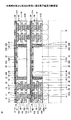
図2は、本発明の第1の実施の形態に係る電子装置の断面図である。
また、電子部品22としては、例えば、CPU用の半導体チップを用いることができる。
図18は、本発明の第2の実施の形態に係る電子装置の断面図である。図18において、第1の実施の形態の電子装置10と同一構成部分には、同一符号を付す。
図21は、本発明の第3の実施の形態に係る電子装置の断面図である。図21において、第2の実施の形態の電子装置90と同一構成部分には、同一符号を付す。
図22は、本発明の第4の実施の形態に係る電子装置の断面図である。図22において、第1及び第3の実施の形態の電子装置10,120と同一構成部分には、同一符号を付す。
11−1,11−2,61,91−1,91−2,121−1,121−2,141−1,141−2 半導体装置
13 内部接続端子
15 実装基板
16 外部接続端子
21,63,93,123 配線基板
22,65 電子部品
22A 電極パッド形成面
22B 背面
23 封止樹脂
25 配線パターン
26,76,77 ソルダーレジスト層
31 多層配線構造体
23A,23B,31A,31B,65A,81A,82A,85A,86A,88A,125A,125B 面
33,128,151 貫通電極
35,131 貫通部
36,40,132,154 貫通孔
38 ビア部
38A,41A,101A 第1の接続面
38B,42A,102A 第2の接続面
41,42,47,48 パッド部
45,79 電極パッド
45A 接続面
49 配線部
51,76A,77A 開口部
67 モールド樹脂
68 金属ワイヤ
71 基板本体
71A 上面
71B 下面
73,74,101,102 パッド
81 支持体
82,143 接着剤
85 樹脂シート
86 第1の封止樹脂
88 第2の封止樹脂
95 導体パターン
103,104 ビア
105 配線
125 シリコン基板
126 絶縁膜
126A 上面
126B 下面
128A 上端面
128B 下端面
145 ピン端子
155 はんだ
157 頭部
158 ピン部
Claims (16)
- 第1の面、該第1の面の反対側に位置する第2の面、及び前記第1の面から前記第2の面に貫通し電子部品を収容する貫通部、を有する配線構造体と、
前記第1の面側に設けられた第1のパッド部、前記第2の面側に設けられた第2のパッド部、及び前記第1のパッド部と前記第2のパッド部とを電気的に接続する接続部、を有し、前記貫通部の周囲に設けられた導体パターンと、
電極パッドが形成された電極パッド形成面、及び該電極パッド形成面の反対側に配置された背面を、有し、前記貫通部に収容された電子部品と、
前記貫通部に充填され、前記電極パッドの表面を露出する第1の平面及び前記電子部品の背面を露出する第2の平面を有する封止樹脂と、
前記第1の平面上に設けられ、前記電極パッドと前記第1のパッド部とを電気的に接続する配線パターンと、を備え、
前記第1の平面、前記電極パッドの表面、及び前記第1のパッド部の表面とが面一であることを特徴とする半導体装置。 - 前記第2の平面、前記電子部品の背面、及び前記第2のパッド部の表面を同一平面上に配置したことを特徴とする請求項1記載の半導体装置。
- 前記封止樹脂は、前記貫通部内に露出した前記配線構造体の側面、及び前記電極パッド形成面に設けられていることを特徴とする請求項1又は2記載の半導体装置。
- 前記封止樹脂は、前記貫通部、前記電極パッド形成面、前記第1の面、及び前記第2の面に設けられていることを特徴とする請求項1又は2記載の半導体装置。
- 前記導体パターンは貫通電極であり、
前記電極パッドを含む前記電子部品の厚さは、前記第1パッド部及び前記第2のパッド部を含む前記貫通電極の厚さと等しいことを特徴とする請求項1ないし4のうち、いずれか1項記載の半導体装置。 - 前記導体パターンは前記配線構造体に内設されており、互いに電気的に接続された前記第1のパッド部、前記第2のパッド部、ビア、及び配線、を有し、
前記電極パッドを含む前記電子部品の厚さは、前記配線構造体の厚さと等しいことを特徴とする請求項1ないし3のうち、いずれか1項記載の半導体装置。 - 前記第1の平面及び前記配線パターンに、前記第1のパッド部を露出する開口部を有したソルダーレジスト層を設けたことを特徴とする請求項1ないし6のうち、いずれか1項記載の半導体装置。
- 第1の面、該第1の面の反対側に位置する第2の面、及び前記第1の面から前記第2の面に貫通し電子部品を収容する貫通部、及び前記第1の面から前記第2の面に貫通し該貫通部の周囲に形成された貫通孔を有するシリコン基板と、
前記貫通孔の側面、前記第1の面、及び前記第2の面に設けられた絶縁膜と、
前記絶縁膜を介して、前記貫通孔に設けられた貫通電極と、
電極パッドが形成された電極パッド形成面、及び該電極パッド形成面の反対側に配置された背面を、有し、前記貫通部に収容された電子部品と、
前記貫通部に充填され、前記電極パッドの表面を露出する第1の平面及び前記電子部品の背面を露出する第2の平面を有する封止樹脂と、
前記第1の平面上に設けられ、前記電極パッドと前記貫通電極とを電気的に接続する配線パターンと、を備え、
前記第1の平面、前記電極パッドの表面、及び前記貫通電極の上端面とが面一であることを特徴とする半導体装置。 - 前記第2の平面、前記電子部品の背面、及び前記貫通電極の下端面を面一にしたことを特徴とする請求項8記載の半導体装置。
- 前記シリコン基板の厚さは、前記電極パッドを含む前記電子部品の厚さと等しいことを特徴とする請求項8又は9記載の半導体装置。
- 第1の面、該第1の面の反対側に位置する第2の面、及び前記第1の面から前記第2の面に貫通し電子部品を収容する貫通部、及び前記第1の面から前記第2の面に貫通し該貫通部の周囲に形成された貫通孔を有するシリコン基板と、
前記貫通孔の側面、前記第1の面、及び前記第2の面に設けられた絶縁膜と、
前記絶縁膜を介して、前記貫通孔に設けられた貫通電極と、
電極パッドが形成された電極パッド形成面、及び該電極パッド形成面の反対側に配置された背面を、有し、前記貫通部に収容された電子部品と、
前記貫通部、前記電極パッド形成面、前記第1の面上、及び前記第2の面上に設けられ、前記電極パッドの表面及び前記貫通電極の上端面を露出する第1の平面並びに前記電子部品の背面及び前記貫通電極の下端面を露出する第2の平面を有する封止樹脂と、
前記第1の平面上に設けられ、前記電極パッドと前記貫通電極とを電気的に接続する配線パターンと、を備え、
前記貫通電極の中央部、及び該貫通電極の中央部と対向する部分の前記配線パターンを貫通すると共に、ピン端子を挿入可能なピン端子挿入用孔を設け、
前記第1の平面、前記電極パッドの表面、及び前記貫通電極の上端面とが面一であることを特徴とする半導体装置。 - 前記第2の平面、前記電子部品の背面、及び前記貫通電極の下端面とを面一にしたことを特徴とする請求項11記載の半導体装置。
- 請求項1ないし7のうち、いずれか1項記載の半導体装置と、
前記半導体装置上に配置された他の半導体装置と、
前記半導体装置と前記他の半導体装置との間に配置され、前記半導体装置と前記他の半導体装置とを電気的に接続する内部接続端子と、を備えたことを特徴とする電子装置。 - 請求項8ないし10のうち、いずれか1項記載の半導体装置を複数有し、
複数の前記半導体装置を積み重ねて配置し、内部接続端子を介して、前記半導体装置間を電気的に接続したことを特徴とする電子装置。 - 請求項11又は12記載の半導体装置を2つ有し、
2つの前記半導体装置を積み重ねて配置し、2つの前記半導体装置に設けられた前記ピン端子挿入用孔に前記ピン端子を挿入することで、2つの前記半導体装置を電気的に接続したことを特徴とする電子装置。 - 第1の面、該第1の面の反対側に位置する第2の面、及び前記第1の面と前記第2の面とを貫通し電子部品を収容する貫通部、を有する配線構造体と、前記第1の面側に設けられた第1のパッド部、及び前記第2の面側に設けられ前記第1のパッド部と電気的に接続された第2のパッド部、を有し、前記貫通部の周囲に設けられた導体パターンと、を備えた配線基板を形成する配線基板形成工程と、
支持体の面に接着剤を形成する接着剤形成工程と、
前記第2のパッド部の表面と前記接着剤とが接触するように、前記接着剤により、前記配線基板を前記支持体に接着する配線基板接着工程と、
電極パッドが形成された電極パッド形成面、及び該電極パッド形成面の反対側に配置された背面を有する電子部品を準備した後、前記電極パッドの表面と前記第1のパッド部の表面とが面一となるように、前記貫通部から露出された部分の前記接着剤と前記電子部品の背面とを接着させる電子部品接着工程と、
前記貫通部に充填され、前記電極パッドの表面を露出する第1の平面及び前記電子部品の背面を露出する第2の平面を有する封止樹脂を形成する封止樹脂形成工程と、
前記第1の平面上に設けられ、前記電極パッドと前記第1のパッド部とを電気的に接続する配線パターンを形成する配線パターン形成工程と、
前記接着剤及び前記支持体を除去する接着剤及び支持体除去工程と、を含むことを特徴とする半導体装置の製造方法。
Priority Applications (2)
| Application Number | Priority Date | Filing Date | Title |
|---|---|---|---|
| JP2009077033A JP5106460B2 (ja) | 2009-03-26 | 2009-03-26 | 半導体装置及びその製造方法、並びに電子装置 |
| US12/730,455 US8669653B2 (en) | 2009-03-26 | 2010-03-24 | Semiconductor device having electronic component in through part, electronic device, and manufacturing method of semiconductor |
Applications Claiming Priority (1)
| Application Number | Priority Date | Filing Date | Title |
|---|---|---|---|
| JP2009077033A JP5106460B2 (ja) | 2009-03-26 | 2009-03-26 | 半導体装置及びその製造方法、並びに電子装置 |
Publications (3)
| Publication Number | Publication Date |
|---|---|
| JP2010232333A JP2010232333A (ja) | 2010-10-14 |
| JP2010232333A5 JP2010232333A5 (ja) | 2012-03-29 |
| JP5106460B2 true JP5106460B2 (ja) | 2012-12-26 |
Family
ID=42783089
Family Applications (1)
| Application Number | Title | Priority Date | Filing Date |
|---|---|---|---|
| JP2009077033A Active JP5106460B2 (ja) | 2009-03-26 | 2009-03-26 | 半導体装置及びその製造方法、並びに電子装置 |
Country Status (2)
| Country | Link |
|---|---|
| US (1) | US8669653B2 (ja) |
| JP (1) | JP5106460B2 (ja) |
Cited By (1)
| Publication number | Priority date | Publication date | Assignee | Title |
|---|---|---|---|---|
| US10356907B2 (en) | 2015-08-31 | 2019-07-16 | Olympus Corporation | Endoscope, electronic unit and method for manufacturing electronic unit |
Families Citing this family (14)
| Publication number | Priority date | Publication date | Assignee | Title |
|---|---|---|---|---|
| JP5136632B2 (ja) * | 2010-01-08 | 2013-02-06 | 大日本印刷株式会社 | 電子部品 |
| US8604614B2 (en) * | 2010-03-26 | 2013-12-10 | Samsung Electronics Co., Ltd. | Semiconductor packages having warpage compensation |
| US8669651B2 (en) * | 2010-07-26 | 2014-03-11 | Taiwan Semiconductor Manufacturing Company, Ltd. | Package-on-package structures with reduced bump bridging |
| KR101236798B1 (ko) * | 2011-02-16 | 2013-02-25 | 앰코 테크놀로지 코리아 주식회사 | 웨이퍼 레벨 적층형 반도체 패키지 제조 방법 |
| US8963310B2 (en) | 2011-08-24 | 2015-02-24 | Tessera, Inc. | Low cost hybrid high density package |
| US10115671B2 (en) * | 2012-08-03 | 2018-10-30 | Snaptrack, Inc. | Incorporation of passives and fine pitch through via for package on package |
| KR101515777B1 (ko) * | 2013-04-22 | 2015-05-04 | 주식회사 네패스 | 반도체 패키지 제조방법 |
| US9576909B2 (en) * | 2013-08-21 | 2017-02-21 | Intel Corporation | Bumpless die-package interface for bumpless build-up layer (BBUL) |
| US9691726B2 (en) * | 2014-07-08 | 2017-06-27 | Taiwan Semiconductor Manufacturing Company, Ltd. | Methods for forming fan-out package structure |
| KR102565119B1 (ko) * | 2016-08-25 | 2023-08-08 | 삼성전기주식회사 | 전자 소자 내장 기판과 그 제조 방법 및 전자 소자 모듈 |
| CN110088894B (zh) * | 2016-12-21 | 2023-09-12 | 株式会社村田制作所 | 电子部件内置基板的制造方法、电子部件内置基板、电子部件装置及通信模块 |
| US20200027728A1 (en) * | 2018-07-23 | 2020-01-23 | Intel Corporation | Substrate package with glass dielectric |
| TW202201673A (zh) * | 2020-03-17 | 2022-01-01 | 新加坡商安靠科技新加坡控股私人有限公司 | 半導體裝置和製造半導體裝置的方法 |
| US11715699B2 (en) | 2020-03-17 | 2023-08-01 | Amkor Technology Singapore Holding Pte. Ltd. | Semiconductor devices and methods of manufacturing semiconductor devices |
Family Cites Families (22)
| Publication number | Priority date | Publication date | Assignee | Title |
|---|---|---|---|---|
| JPH01256161A (ja) * | 1988-04-05 | 1989-10-12 | Toshiba Corp | 印刷配線板装置 |
| US5222014A (en) | 1992-03-02 | 1993-06-22 | Motorola, Inc. | Three-dimensional multi-chip pad array carrier |
| US5306670A (en) * | 1993-02-09 | 1994-04-26 | Texas Instruments Incorporated | Multi-chip integrated circuit module and method for fabrication thereof |
| KR100208053B1 (ko) * | 1994-07-04 | 1999-07-15 | 모리시타 요이찌 | 집적회로장치 |
| JP2792494B2 (ja) * | 1996-01-17 | 1998-09-03 | 日本電気株式会社 | 集積回路の実装構造 |
| WO2001063991A1 (fr) * | 2000-02-25 | 2001-08-30 | Ibiden Co., Ltd. | Carte a circuits imprimes multicouche et procede de production d'une carte a circuits imprimes multicouche |
| US20020020898A1 (en) * | 2000-08-16 | 2002-02-21 | Vu Quat T. | Microelectronic substrates with integrated devices |
| US6734534B1 (en) | 2000-08-16 | 2004-05-11 | Intel Corporation | Microelectronic substrate with integrated devices |
| CN100426492C (zh) | 2000-08-16 | 2008-10-15 | 英特尔公司 | 微电子封装件及其制造方法 |
| JP3967108B2 (ja) * | 2001-10-26 | 2007-08-29 | 富士通株式会社 | 半導体装置およびその製造方法 |
| JP3853219B2 (ja) * | 2002-01-18 | 2006-12-06 | イビデン株式会社 | 半導体素子内蔵基板および多層回路基板 |
| JP4167001B2 (ja) * | 2002-04-15 | 2008-10-15 | 日本特殊陶業株式会社 | 配線基板の製造方法 |
| KR20050112122A (ko) * | 2003-04-07 | 2005-11-29 | 이비덴 가부시키가이샤 | 다층프린트배선판 |
| JP2005033141A (ja) * | 2003-07-11 | 2005-02-03 | Sony Corp | 半導体装置及びその製造方法、疑似ウェーハ及びその製造方法、並びに半導体装置の実装構造 |
| JP4955935B2 (ja) * | 2004-05-25 | 2012-06-20 | キヤノン株式会社 | 貫通孔形成方法および半導体装置の製造方法 |
| JP4214969B2 (ja) * | 2004-08-16 | 2009-01-28 | 沖電気工業株式会社 | 半導体装置の製造方法 |
| JP2006202997A (ja) * | 2005-01-20 | 2006-08-03 | Sharp Corp | 半導体装置およびその製造方法 |
| US7919844B2 (en) * | 2005-05-26 | 2011-04-05 | Aprolase Development Co., Llc | Tier structure with tier frame having a feedthrough structure |
| JP4916241B2 (ja) * | 2006-07-28 | 2012-04-11 | パナソニック株式会社 | 半導体装置及びその製造方法 |
| KR100796523B1 (ko) * | 2006-08-17 | 2008-01-21 | 삼성전기주식회사 | 전자부품 내장형 다층 인쇄배선기판 및 그 제조방법 |
| KR101057368B1 (ko) * | 2007-01-31 | 2011-08-18 | 후지쯔 세미컨덕터 가부시키가이샤 | 반도체 장치 및 그 제조 방법 |
| US8130507B2 (en) * | 2008-03-24 | 2012-03-06 | Ngk Spark Plug Co., Ltd. | Component built-in wiring board |
-
2009
- 2009-03-26 JP JP2009077033A patent/JP5106460B2/ja active Active
-
2010
- 2010-03-24 US US12/730,455 patent/US8669653B2/en active Active
Cited By (1)
| Publication number | Priority date | Publication date | Assignee | Title |
|---|---|---|---|---|
| US10356907B2 (en) | 2015-08-31 | 2019-07-16 | Olympus Corporation | Endoscope, electronic unit and method for manufacturing electronic unit |
Also Published As
| Publication number | Publication date |
|---|---|
| JP2010232333A (ja) | 2010-10-14 |
| US20100244230A1 (en) | 2010-09-30 |
| US8669653B2 (en) | 2014-03-11 |
Similar Documents
| Publication | Publication Date | Title |
|---|---|---|
| JP5106460B2 (ja) | 半導体装置及びその製造方法、並びに電子装置 | |
| JP5193898B2 (ja) | 半導体装置及び電子装置 | |
| JP5188426B2 (ja) | 半導体装置及びその製造方法、電子装置 | |
| JP4361826B2 (ja) | 半導体装置 | |
| JP2701802B2 (ja) | ベアチップ実装用プリント基板 | |
| JP4551321B2 (ja) | 電子部品実装構造及びその製造方法 | |
| US6930257B1 (en) | Integrated circuit substrate having laminated laser-embedded circuit layers | |
| JP5193503B2 (ja) | 貫通電極付き基板及びその製造方法 | |
| JP5372579B2 (ja) | 半導体装置及びその製造方法、並びに電子装置 | |
| JP5280945B2 (ja) | 半導体装置及びその製造方法 | |
| JP5219276B2 (ja) | 電子素子内蔵型印刷回路基板の製造方法 | |
| JP4800606B2 (ja) | 素子内蔵基板の製造方法 | |
| JP2009194322A (ja) | 半導体装置の製造方法、半導体装置及び配線基板 | |
| JP4070470B2 (ja) | 半導体装置用多層回路基板及びその製造方法並びに半導体装置 | |
| JPWO2011024939A1 (ja) | 半導体装置およびその製造方法 | |
| JP2007067120A (ja) | 回路基板およびそれを用いた回路装置 | |
| KR102117477B1 (ko) | 반도체 패키지 및 반도체 패키지의 제조방법 | |
| KR100923501B1 (ko) | 패키지 기판 제조방법 | |
| TWI407542B (zh) | 嵌埋半導體元件之電路板及其製法 | |
| CN113838829B (zh) | 封装载板及其制作方法 | |
| KR101257457B1 (ko) | 집적회로 칩이 내장된 인쇄회로기판의 제조 방법 | |
| CN101494205B (zh) | 集成电路封装体及其制造方法 | |
| JP2000174440A (ja) | 多層回路基板及びその製造方法 | |
| JP2010103290A (ja) | 半導体装置の製造方法 | |
| JP2021036574A (ja) | プリント配線板の製造方法及びプリント配線板 |
Legal Events
| Date | Code | Title | Description |
|---|---|---|---|
| A521 | Request for written amendment filed |
Free format text: JAPANESE INTERMEDIATE CODE: A523 Effective date: 20120210 |
|
| A621 | Written request for application examination |
Free format text: JAPANESE INTERMEDIATE CODE: A621 Effective date: 20120210 |
|
| A977 | Report on retrieval |
Free format text: JAPANESE INTERMEDIATE CODE: A971007 Effective date: 20120903 |
|
| TRDD | Decision of grant or rejection written | ||
| A01 | Written decision to grant a patent or to grant a registration (utility model) |
Free format text: JAPANESE INTERMEDIATE CODE: A01 Effective date: 20120925 |
|
| A01 | Written decision to grant a patent or to grant a registration (utility model) |
Free format text: JAPANESE INTERMEDIATE CODE: A01 |
|
| A61 | First payment of annual fees (during grant procedure) |
Free format text: JAPANESE INTERMEDIATE CODE: A61 Effective date: 20121002 |
|
| R150 | Certificate of patent or registration of utility model |
Ref document number: 5106460 Country of ref document: JP Free format text: JAPANESE INTERMEDIATE CODE: R150 Free format text: JAPANESE INTERMEDIATE CODE: R150 |
|
| FPAY | Renewal fee payment (event date is renewal date of database) |
Free format text: PAYMENT UNTIL: 20151012 Year of fee payment: 3 |