JP5103006B2 - Manufacturing method of semiconductor device - Google Patents
Manufacturing method of semiconductor device Download PDFInfo
- Publication number
- JP5103006B2 JP5103006B2 JP2006310464A JP2006310464A JP5103006B2 JP 5103006 B2 JP5103006 B2 JP 5103006B2 JP 2006310464 A JP2006310464 A JP 2006310464A JP 2006310464 A JP2006310464 A JP 2006310464A JP 5103006 B2 JP5103006 B2 JP 5103006B2
- Authority
- JP
- Japan
- Prior art keywords
- etching
- insulating film
- manufacturing
- semiconductor device
- condition
- Prior art date
- Legal status (The legal status is an assumption and is not a legal conclusion. Google has not performed a legal analysis and makes no representation as to the accuracy of the status listed.)
- Active
Links
Images


Classifications
-
- H10P50/692—
-
- H10P50/283—
-
- H10P50/287—
-
- H10W20/081—
Landscapes
- Engineering & Computer Science (AREA)
- Drying Of Semiconductors (AREA)
- Manufacturing & Machinery (AREA)
- Physics & Mathematics (AREA)
- Condensed Matter Physics & Semiconductors (AREA)
- General Physics & Mathematics (AREA)
- Computer Hardware Design (AREA)
- Microelectronics & Electronic Packaging (AREA)
- Power Engineering (AREA)
- Internal Circuitry In Semiconductor Integrated Circuit Devices (AREA)
- Chemical & Material Sciences (AREA)
- Chemical Kinetics & Catalysis (AREA)
- General Chemical & Material Sciences (AREA)
- Inorganic Chemistry (AREA)
Description
本発明は、半導体装置の製造方法に関する。 The present invention relates to a method for manufacturing a semiconductor device.
今日、製造コストが安価であるデュアルダマシン法を用いたCu配線が主流である。配線溝のエッチング深さは、後続の工程で埋め込まれるCu配線の断面積に直接作用し配線抵抗や配線容量に影響を与える。したがって、デュアルダマシン法においては、配線溝のエッチング深さの均一性や安定化が特に重要である。 Today, Cu wiring using the dual damascene method, which is inexpensive to manufacture, is the mainstream. The etching depth of the wiring groove directly affects the cross-sectional area of the Cu wiring embedded in the subsequent process and affects the wiring resistance and the wiring capacity. Therefore, in the dual damascene method, the uniformity and stabilization of the etching depth of the wiring trench is particularly important.
特許文献1には、デュアルダマシン法におけるエッチングの方法が開示されている。この方法では、SiO2より比誘電率が低い、いわゆる低誘電率膜とそれを覆うSiO2膜(キャップ膜)とを別々のエッチング条件でエッチングし、配線溝を形成している。具体的には、低誘電率膜に対して選択比が大きい条件でSiO2膜をエッチングした後、低誘電率膜に対して選択比が小さい条件で低誘電率膜をエッチングしている。
なお、本発明に関連する先行技術文献としては、特許文献1の他に、特許文献2〜4が挙げられる。
第1の絶縁膜上に第2の絶縁膜が形成されたものを順次エッチングする際に、第2の絶縁膜のエッチングを第1の絶縁膜が露出したところで停止させると、第2の絶縁膜のエッチング時に溝の底部に形成されたデポジション膜の厚みがウエハ面内で大きく異なることを本発明者が新たに見出した。この厚みが異なることにより、第1の絶縁膜を加工した後の加工形状の面内均一性が悪くなる。 When sequentially etching the second insulating film formed on the first insulating film, the second insulating film is stopped when the etching of the second insulating film is stopped when the first insulating film is exposed. The inventor newly found that the thickness of the deposition film formed on the bottom of the groove during the etching differs greatly within the wafer surface. Due to the difference in thickness, the in-plane uniformity of the processed shape after processing the first insulating film is deteriorated.
本発明による半導体装置の製造方法は、第1の絶縁膜と上記第1の絶縁膜上に設けられた第2の絶縁膜とを備える半導体装置を製造する方法であって、第1のエッチング条件で、上記第2の絶縁膜を途中までエッチングする第1のエッチング工程と、上記第1のエッチング条件とは異なる第2のエッチング条件で、上記第1のエッチング工程において残された上記第2の絶縁膜の残部と、上記第1の絶縁膜とをエッチングする第2のエッチング工程と、を含むことを特徴とする。 A method of manufacturing a semiconductor device according to the present invention is a method of manufacturing a semiconductor device including a first insulating film and a second insulating film provided on the first insulating film, wherein the first etching condition is In the first etching step for etching the second insulating film halfway and the second etching condition different from the first etching condition, the second etching step left in the first etching step is performed. And a second etching step of etching the remaining portion of the insulating film and the first insulating film.
この製造方法においては、第2の絶縁膜のエッチングを途中で一旦停止し、その後に第2の絶縁膜の残部と第1の絶縁膜とを一括してエッチングする。このように第1のエッチング工程の直後に第1の絶縁膜を露出させないことで、不均一な厚みを有するデポジション膜が堆積されるのを防ぐことができる。これにより、第1の絶縁膜を加工した後の加工形状の面内均一性が向上する。 In this manufacturing method, the etching of the second insulating film is temporarily stopped in the middle, and then the remaining part of the second insulating film and the first insulating film are collectively etched. Thus, by not exposing the first insulating film immediately after the first etching step, it is possible to prevent the deposition film having a non-uniform thickness from being deposited. Thereby, the in-plane uniformity of the processed shape after processing the first insulating film is improved.
本発明によれば、絶縁膜のエッチング加工形状についてウエハ面内で高い均一性を得ることが可能な半導体装置の製造方法が実現される。 According to the present invention, a semiconductor device manufacturing method capable of obtaining high uniformity in the wafer surface with respect to the etched shape of the insulating film is realized.
以下、図面を参照しつつ、本発明による半導体装置の製造方法の好適な実施形態について詳細に説明する。なお、図面の説明においては、同一要素には同一符号を付し、重複する説明を省略する。 Hereinafter, preferred embodiments of a method of manufacturing a semiconductor device according to the present invention will be described in detail with reference to the drawings. In the description of the drawings, the same reference numerals are assigned to the same elements, and duplicate descriptions are omitted.
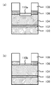
図1および図2は、本発明による半導体装置の製造方法の一実施形態を示す工程図である。この製造方法は、低誘電率膜10(第1の絶縁膜)と低誘電率膜10上に設けられたキャップ膜20(第2の絶縁膜)とを備える半導体装置を製造する方法である。これらの低誘電率膜10とキャップ膜20との間には、エッチングストップ膜が介在していない。
1 and 2 are process diagrams showing an embodiment of a method of manufacturing a semiconductor device according to the present invention. This manufacturing method is a method of manufacturing a semiconductor device including a low dielectric constant film 10 (first insulating film) and a cap film 20 (second insulating film) provided on the low dielectric
低誘電率膜10の比誘電率は、3.5以下であることが好ましい。低誘電率膜10を構成する材料としては、例えば、ポリオルガノシロキサン、芳香族含有有機材料、HSQ(ハイドロジェンシルセスキオキサン)、SOG(Spin On Glass)、またはFOX(Flowable Oxide)を用いることができる。ポリオルガノシロキサンの例としては、SiOC、MSQ(メチルシルセスキオキサン)、およびMHSQ(メチル化ハイドロジェンシルセスキオキサン)等が挙げられる。SiOCを材料とした低誘電率膜には、例えば、アプライドマテリアル社製のBlack Diamond(登録商標、以下「BD」という)、ノベラシステムズ社製のCoral、およびASM社製のAurolaがある。
The relative dielectric constant of the low dielectric
また、芳香族含有有機材料の例としては、ポリフェニレン、ポリアリールエーテル(PAE)、およびジビニルシロキサン−ビス−ベンゾシクロブテン等が挙げられる。ポリフェニレンを材料とした低誘電率膜には、例えば、ダウケミカル社製のSiLK(登録商標)がある。また、ポリアニールエーテルを材料とした低誘電率膜には、例えば、ハネウェル社製のFlareがある。なお、低誘電率膜10は、ポーラス状をしていてもよい。
Examples of the aromatic-containing organic material include polyphenylene, polyaryl ether (PAE), divinylsiloxane-bis-benzocyclobutene, and the like. An example of a low dielectric constant film made of polyphenylene is SiLK (registered trademark) manufactured by Dow Chemical Company. An example of a low dielectric constant film made of polyanneal ether is Flare manufactured by Honeywell. The low dielectric
キャップ膜20を構成する材料としては、SiO2、SiC、SiCN、SiNまたはBCB(ベンゾシクロブテン)等が挙げられる。
Examples of the material constituting the
まず、レジスト30をマスクとして、第1のエッチング条件でキャップ膜20を途中までエッチングする(第1のエッチング工程)(図1)。第1のエッチング条件は、キャップ膜20の加工に適した条件、すなわち高い均一性でキャップ膜20を加工できるような条件であることが好ましい。また、第1のエッチング工程におけるエッチング時間は、キャップ膜20を最後までエッチングするのに必要なエッチング時間(終点時間)の60%以上90%以下であることが好ましい。キャップ膜20を最後までエッチングするのに必要なエッチング時間は、例えば、EPD(End Point Detector)システムを用いて求めることができる。このエッチング時間に関する条件は、第1のエッチング工程において残されたキャップ膜20の残部22の厚みt1はキャップ膜20全体の厚みt2の10%以上40%以下である、という条件に相当する。
First, the
次に、第1のエッチング条件とは異なる第2のエッチング条件で、キャップ膜20の残部22と低誘電率膜10とを一括してエッチングする(第2のエッチング工程)(図2)。本実施形態において、第1および第2のエッチング工程は、相異なる高周波出力を有する上部電極および下部電極を有するエッチング装置を用いて実行される。また、これらのエッチング工程は、例えばデュアルダマシン工程の一部として実行される。なお、第2のエッチング工程は、第1のエッチング工程が終了した直後に開始してもよいし、所定の時間(安定化時間)を置いてから開始してもよい。安定化時間は、例えば3秒程度である。
Next, the
第2のエッチング条件は、低誘電率膜10およびキャップ膜20間の選択比が実質的に取れない条件であることが好ましい。また、第2のエッチング条件においては、第1のエッチング条件よりも酸素流量が多いことが好ましい。第2のエッチング条件における酸素混合比は、好ましくは、0.4%以上2.6%以下である。さらに、第2のエッチング条件においては、第1のエッチング条件よりも、上部電極の高周波出力(以下、「トップパワー」という)が高いことが好ましい。第2のエッチング条件におけるトップパワーは、好ましくは、1300W以上2200W以下である。
It is preferable that the second etching condition is a condition in which a selection ratio between the low dielectric
第1のエッチング条件の好ましい例は、次のとおりである。CH4−nFn(nは4以下の自然数)を主成分としたガスを使用し、圧力が30mTorr以上60mTorr以下、トップパワーが200W以上600W以下、バイアス出力が700W以上1300W以下、Ar流量が0.9l/min(900sccm)以上1.8l/min(1800sccm)以下である。 A preferred example of the first etching condition is as follows. A gas mainly composed of CH 4-n F n (n is a natural number of 4 or less) is used, the pressure is 30 mTorr to 60 mTorr, the top power is 200 W to 600 W, the bias output is 700 W to 1300 W, and the Ar flow rate is It is 0.9 l / min (900 sccm) or more and 1.8 l / min (1800 sccm) or less.
一方、第2のエッチング条件の好ましい例は、次のとおりである。CH4−nFn(nは4以下の自然数)を主成分としたガスを使用し、圧力が30mTorr以上60mTorr以下、トップパワーが1300W以上2200W以下、バイアス出力が600W以上1200W以下、Ar流量が0.2l/min(200sccm)以上0.6l/min(600sccm)以下である。 On the other hand, a preferred example of the second etching condition is as follows. A gas mainly composed of CH 4-n F n (n is a natural number of 4 or less) is used, the pressure is 30 mTorr to 60 mTorr, the top power is 1300 W to 2200 W, the bias output is 600 W to 1200 W, and the Ar flow rate is It is 0.2 l / min (200 sccm) or more and 0.6 l / min (600 sccm) or less.
なお、ガス流量は、ウエハの中央部付近の方が端部付近よりも多い(例えば分圧比で9:1)場合がある。その場合、本明細書中に例示するガス流量は、ウエハ中央部付近におけるものを示している。 In some cases, the gas flow rate is higher in the vicinity of the center of the wafer than in the vicinity of the end (for example, the partial pressure ratio is 9: 1). In that case, the gas flow rate exemplified in the present specification indicates that in the vicinity of the center of the wafer.
本実施形態の効果を説明する。本実施形態においては、キャップ膜20のエッチングを途中で一旦停止し、その後にキャップ膜20の残部22と低誘電率膜10とを一括してエッチングする。このように第1のエッチング工程の直後に低誘電率膜10を露出させないことで、不均一な厚みを有するデポジション膜が堆積されるのを防ぐことができる。これにより、低誘電率膜10を加工した後の加工形状の面内均一性が向上する。
The effect of this embodiment will be described. In the present embodiment, the etching of the
これに対し、特許文献1の方法では、上述のとおり、第1の絶縁膜を加工した後の加工形状の面内均一性が悪くなる。この問題の具体例を説明する。エッチングは、一般的にウエハ上に堆積するデポジションとウエハに突入するイオンとの競争反応によって進行する。このとき、デポジションが堆積する速度およびその均一性は、膜種によって異なる。また、SiO2膜と低誘電率膜との間には、エッチング特性の差がある。例えば、SiO2膜は物理的なスパッタリング要素がないとエッチングが進行しにくいのに対し、カーボンや水素を含有した低誘電率膜は物理的なスパッタリングよりもむしろ化学的にエッチングが進行し易い。
On the other hand, in the method of
したがって、図15に示すように、SiO2膜106のエッチング中は、溝の中に堆積するデポジションP1と溝の中に突入するイオンP2のバランスがとれるため、デポジションの量についてウエハ面内で良好な均一性が維持される。ところが、下地の低誘電率膜104が露出した途端に、低誘電率膜104から発生するカーボンや水素等のデポジション成分の相違と、低誘電率膜104に対するデポジションの付着確率の相違により、低誘電率膜104上に堆積するデポジションのバランスが崩れてしまう。このときのウエハ中央部付近およびウエハ端部付近の様子を、それぞれ図16(a)および図16(b)に示す。これらの図においては、層間絶縁膜100上に、ビアストッパ102、低誘電率膜104、キャップ膜106およびレジスト108が順に積層されている。層間絶縁膜100中には、トランジスタ等の素子や配線(共に図示せず)等が形成されている。
Therefore, as shown in FIG. 15, during the etching of the SiO 2 film 106, the deposition P1 deposited in the groove and the ions P2 entering the groove can be balanced. Good uniformity is maintained. However, as soon as the underlying low dielectric
そのため、図17(a)および図17(b)に示すように、ウエハ中央部付近のデポジション膜110aの方が、ウエハ端部付近のデポジション膜110bよりも厚くなる。すると、図18(a)および図18(b)に示すように、低誘電率膜104をエッチングする際、ウエハ中央部付近でのエッチング深さd1が、ウエハ端部付近でのエッチング深さd2よりも小さくなる。このように、デポジション膜の厚みの相違に起因してウエハ面内でのエッチング深さ等の均一性が損なわれてしまう。この点、本実施形態によれば、エッチング深さについてもウエハ面内で高い均一性が得られる。
For this reason, as shown in FIGS. 17A and 17B, the
また、低誘電率膜10上にデポジション膜が堆積した場合、それを除去するための時間が余計にかかるため、スループットが低下し、生産効率も低下してしまう。本実施形態によれば、かかる問題も回避することができる。
In addition, when a deposition film is deposited on the low dielectric
ところで、低誘電率膜10上にキャップ膜20を成膜する際に、それらの間に変質層が生じてしまうことがある。この変質層は、例えば、SiONライクな材料からなる層である。キャップ膜20をCVD法により成膜する場合、その原料ガスが不必要な反応を起こすことが、変質層が形成される原因と考えられる。厄介なことに、この変質層の存在も、デポジション膜と同様に、ウエハ面内でのエッチング深さの均一性を損なう要因となる。ウエハ中央部付近の変質層の方が、ウエハ端部付近のそれよりも厚くなるからである。この点、本実施形態によれば、かかる変質層が存在する場合であっても、変質層に対する選択比も小さくなるように第2のエッチング条件を設定することで、当該変質層の影響を充分に小さく抑えることができる。このため、変質層に起因するエッチング深さの不均一性を緩和することができる。
By the way, when the
本実施形態においては、さらに、低誘電率膜10上にキャップ膜20が設けられている。これにより、CMP(Chemical Mechanical Polishing)の際に低誘電率膜10が損傷を受けるのを防ぐとともに、低誘電率膜10の吸湿を防ぐことができる。
In the present embodiment, a
また、低誘電率膜10およびキャップ膜20間にエッチングストップ膜が介在していない。これにより、半導体装置の製造コストを低減することができる。これに対して、特許文献2に記載された半導体装置のようにエッチングストップ膜を設ける場合、当該エッチングストップ膜の形成、およびその上の層間絶縁膜の形成の分だけ成膜回数が増加し、製造コストが増大してしまう。
Further, no etching stop film is interposed between the low dielectric
第1のエッチング工程におけるエッチング時間が終点時間の60%以上90%以下である場合、ウエハ面内でのエッチング深さの均一性を特に高めることができる。この点に関し、エッチング時間とエッチング深さのバラツキとの関係を調べた実験の結果を図3〜図5に示す。当該実験においてはキャップ膜20としてSiO2膜を用いた。また、第1のエッチング条件すなわちSiO2膜のエッチング条件は、圧力が40mTorr、トップパワーが300W、バイアス出力が1000W、CHF3流量が0.035l/min(35sccm)、CF4流量が0.055l/min(55sccm)、Ar流量が0.9l/min(900sccm)とした。
When the etching time in the first etching step is 60% or more and 90% or less of the end point time, the uniformity of the etching depth in the wafer surface can be particularly improved. In this regard, the results of experiments examining the relationship between the etching time and the variation in etching depth are shown in FIGS. In the experiment, a SiO 2 film was used as the
図3(a)および図3(b)は、エッチング時間を終点時間の70%とした場合の結果を示すグラフである。これらのグラフの横軸は、ラインアンドスペースのパターンの寸法、すなわちライン幅(nm)/スペース幅(nm)を表している。また、縦軸は、図3(a)ではエッチング深さ(nm)を、図3(b)ではエッチング深さの差(nm)を表している。エッチング深さは、ウエハの中央部(cntr)、および端部から7mmの部分の各々について測定した。後者から前者を減じた値を、エッチング深さの差とした。 FIG. 3A and FIG. 3B are graphs showing the results when the etching time is 70% of the end point time. The horizontal axis of these graphs represents the dimension of the line and space pattern, that is, the line width (nm) / space width (nm). The vertical axis represents the etching depth (nm) in FIG. 3A and the etching depth difference (nm) in FIG. 3B. The etching depth was measured for each of a central portion (cntr) of the wafer and a portion 7 mm from the end portion. The difference obtained by subtracting the former from the latter was taken as the difference in etching depth.
図4(a)および図4(b)はエッチング時間を終点時間の85%とした場合の結果を、図5(a)および図5(b)はエッチング時間を終点時間の95%とした場合の結果を示している。図4(a)および図5(a)のグラフの意味は、図3(a)と同様である。また、図4(b)および図5(b)のグラフの意味は、図3(b)と同様である。 4A and 4B show the results when the etching time is 85% of the end time, and FIGS. 5A and 5B show the results when the etching time is 95% of the end time. Shows the results. The meanings of the graphs in FIGS. 4A and 5A are the same as those in FIG. The meanings of the graphs in FIGS. 4B and 5B are the same as those in FIG. 3B.
これらのグラフを比較すると、エッチング時間が上記範囲(終点時間の60%以上90%以下)外にある場合(図5参照)よりも、エッチング時間が上記範囲内にある場合(図3または図4参照)の方が、エッチング深さのバラツキが小さいことがわかる。 When these graphs are compared, when the etching time is within the above range (see FIG. 3 or FIG. 4) than when the etching time is outside the above range (60% to 90% of the end point time) (see FIG. 5). It can be seen that the variation in the etching depth is smaller.
また、図6(a)および図6(b)は、本実施形態を適用した場合におけるSiO2膜のエッチングレートのウエハ面内分布を測定した結果を示すグラフである。一方、図7(a)および図7(b)は、本実施形態を適用しない場合におけるSiO2膜のエッチングレートのウエハ面内分布を測定した結果を示すグラフである。これらのグラフの横軸はウエハの中心を原点とした位置(mm)を表し、縦軸はエッチングレート(nm/min)を表している。また、X-axisはウエハのノッチを下にしたときの左右方向であり、Y-axisはそれに垂直な方向すなわち上下方向である。図6(a)および図7(a)はエッチング装置のチャンバ内部のパーツが磨耗した後に測定した結果を、図6(b)および図7(b)は同パーツが新品の状態で測定した結果を示している。 FIGS. 6A and 6B are graphs showing the results of measuring the in-wafer distribution of the etching rate of the SiO 2 film when the present embodiment is applied. On the other hand, FIGS. 7A and 7B are graphs showing the results of measuring the in-wafer distribution of the etching rate of the SiO 2 film when the present embodiment is not applied. The horizontal axis of these graphs represents the position (mm) with the center of the wafer as the origin, and the vertical axis represents the etching rate (nm / min). X-axis is the left-right direction when the notch of the wafer is down, and Y-axis is the direction perpendicular to it, that is, the up-down direction. 6 (a) and 7 (a) show the measurement results after the parts inside the chamber of the etching apparatus are worn, and FIGS. 6 (b) and 7 (b) show the measurement results when the parts are new. Is shown.
これらのグラフを比較すると、本実施形態を適用しない場合(図7参照)にはパーツの磨耗度合いによってエッチングレートの分布が変化するのに対して、本実施形態を適用した場合(図6参照)にはエッチングレートの分布がパーツの磨耗度合いに依存しないことがわかる。このように、本実施形態による製造方法は、長期安定性にも優れている。 Comparing these graphs, when the present embodiment is not applied (see FIG. 7), the etching rate distribution changes depending on the degree of wear of the parts, whereas the present embodiment is applied (see FIG. 6). It can be seen that the etching rate distribution does not depend on the degree of wear of the parts. Thus, the manufacturing method according to the present embodiment is excellent in long-term stability.
第2のエッチング条件における酸素混合比が0.4%以上である場合、ウエハ面内でのエッチング深さの均一性を特に高めることができる。さらに、その酸素混合比が2.6%以下である場合、レジスト30に対する選択比を充分に確保でき、ラフネスを小さく抑えることができる。 When the oxygen mixing ratio in the second etching condition is 0.4% or more, the uniformity of the etching depth within the wafer surface can be particularly improved. Furthermore, when the oxygen mixing ratio is 2.6% or less, a sufficient selection ratio with respect to the resist 30 can be secured, and the roughness can be kept small.
この点に関し、第2のエッチング工程における酸素混合量とエッチング深さのバラツキとの関係を調べた実験の結果を図8および図9に示す。当該実験においては低誘電率膜10としてBDを用いた。また、第2のエッチング条件は、圧力が40mTorr、トップパワーが1900W、バイアス出力が600W、CHF3流量が0.023l/min(23sccm)、CF4流量が0.023l/min(23sccm)、Ar流量が0.4l/min(400sccm)とした。この場合、酸素混合比が0.4%以上2.6%以下という条件は、O2流量が0.002l/min(2sccm)以上0.012l/min(12sccm)以下という条件に相当する。図8および図9では、それぞれO2流量を0.003l/min(3sccm)および0.006l/min(6sccm)とした。その他の条件は、図3〜図5について説明したとおりである。図8(a)および図9(a)のグラフの意味は、図3(a)と同様である。また、図8(b)および図9(b)のグラフの意味は、図3(b)と同様である。
In this regard, FIG. 8 and FIG. 9 show the results of an experiment examining the relationship between the oxygen mixing amount and the etching depth variation in the second etching step. In this experiment, BD was used as the low dielectric
これらのグラフを比較すると、O2混合量の増大に伴い、主にウエハ中央部付近でのエッチングレートが増大し、その結果エッチング深さのバラツキが減少していることがわかる。これは、O2が上述したデポジションを減少させる働きを有するためであると考えられる。 Comparing these graphs, it can be seen that the etching rate mainly near the center of the wafer increases as the O 2 mixing amount increases, and as a result, the variation in etching depth decreases. This is considered to be because O 2 has a function of reducing the above-described deposition.
第2のエッチング条件におけるトップパワーが1300W以上2200W以下である場合、ウエハ面内でのエッチング深さの均一性を特に高めることができる。この点に関し、トップパワーとエッチング深さのバラツキとの関係を調べた実験の結果を図10〜図12に示す。図10、図11および図12は、それぞれトップパワーを1000W、1400Wおよび1600Wとした場合の結果を示している。図10(a)、図11(a)および図12(a)のグラフの意味は、図3(a)と同様である。また、図10(b)、図11(b)および図12(b)のグラフの意味は、図3(b)と同様である。 When the top power in the second etching condition is 1300 W or more and 2200 W or less, the uniformity of the etching depth in the wafer surface can be particularly improved. In this regard, the results of experiments examining the relationship between top power and variation in etching depth are shown in FIGS. 10, FIG. 11, and FIG. 12 show the results when the top power is 1000 W, 1400 W, and 1600 W, respectively. The meanings of the graphs in FIGS. 10A, 11A, and 12A are the same as those in FIG. Moreover, the meaning of the graph of FIG.10 (b), FIG.11 (b), and FIG.12 (b) is the same as that of FIG.3 (b).
これらのグラフを比較すると、トップパワーの増大に伴い、主にウエハ中央部付近でのエッチングレートが増大し、その結果エッチング深さのバラツキが減少していることがわかる。トップパワーの増大は、ガスの進行を促進させ、Fリッチなプラズマが生成する。さらに、電子密度は、ウエハ中央部で増大し易い。そのため、特にウエハ中央部付近でFリッチな状態が作り出され、その部分でのエッチングレートが増大し、結果的にエッチング深さの差が縮小したものと考えられる。 Comparing these graphs, it can be seen that the etching rate mainly increases near the center of the wafer as the top power increases, and as a result, the variation in etching depth decreases. The increase in the top power promotes the progress of the gas, and F-rich plasma is generated. Furthermore, the electron density tends to increase at the wafer center. For this reason, it is considered that an F-rich state is created particularly near the center of the wafer, the etching rate at that portion increases, and as a result, the difference in etching depth is reduced.
ところで、エッチング装置においては、ウエハを固定するステージの周りに様々な消耗部品が存在する。例えば、ウエハの周囲に存在する、Si製のフォーカスリンクの磨耗は、ウエハ上部を通過するガスの流れに影響し、主にウエハ上に堆積するデポジションの膜厚や膜質に影響を与える。また、ステージ周囲にあるため、その磨耗度合いにより抵抗値が変動するため、プラズマの収束状態にも影響し、やはりウエハ上面に堆積するデポジションの膜質や膜厚、およびウエハに突入するイオンの向きや量にも影響を与える。この現象のため、生産に使用している装置ではパーツの磨耗度合いに応じて日々チャンバの状態が変動し、ウエハの中央部と端部との間でエッチング深さが変動する等のプロセスシフトが発生する。したがって、消耗部品の変動がプロセス特性に影響しにくい条件が、非常に重要になる。 Incidentally, in the etching apparatus, there are various consumable parts around the stage for fixing the wafer. For example, wear of a focus link made of Si existing around the wafer affects the flow of gas passing through the upper portion of the wafer, and mainly affects the film thickness and film quality of the deposition deposited on the wafer. In addition, since the resistance value varies depending on the degree of wear because it is around the stage, it also affects the plasma convergence state, and also the film quality and thickness of the deposition deposited on the wafer top surface, and the direction of ions entering the wafer Also affects the amount. Because of this phenomenon, in the equipment used for production, the state of the chamber fluctuates every day according to the degree of wear of the parts, and there is a process shift such as the etching depth fluctuating between the center and end of the wafer appear. Therefore, a condition in which fluctuations in consumable parts are unlikely to affect the process characteristics becomes very important.
これに関連して、図13(a)および図13(b)は、本実施形態を適用した場合におけるエッチング深さのウエハ面内分布を測定した結果を示す図である。一方、図14(a)および図14(b)は、本実施形態を適用しない場合におけるエッチング深さのウエハ面内分布を測定した結果を示す図である。これら測定にはOCD(Optical Critical Dimension)測定を用い、ライン幅およびスペース幅が共に140nmであるパターンを対象とした。また、各図の表中のUniformityは、(max.−min.)/(2×Average)×100という式に従って算出した値である。図13(a)および図14(a)はエッチング装置のチャンバ内部のパーツが磨耗した後に測定した結果を、図13(b)および図14(b)は同パーツが新品の状態で測定した結果を示している。 In relation to this, FIG. 13A and FIG. 13B are diagrams showing the results of measuring the in-wafer distribution of the etching depth when this embodiment is applied. On the other hand, FIG. 14A and FIG. 14B are diagrams showing the results of measuring the in-wafer distribution of the etching depth when the present embodiment is not applied. For these measurements, OCD (Optical Critical Dimension) measurement was used, and a pattern having both a line width and a space width of 140 nm was used. Moreover, Uniformity in the table | surface of each figure is the value computed according to the formula of (max.-min.) / (2 * Average) * 100. FIGS. 13 (a) and 14 (a) show the measurement results after the parts inside the chamber of the etching apparatus are worn, and FIGS. 13 (b) and 14 (b) show the measurement results when the parts are new. Is shown.
これらの測定結果を比較すると、本実施形態を適用しない場合(図14参照)にはパーツの磨耗度合いによってエッチング深さのバラツキが変化するのに対して、本実施形態を適用した場合(図13参照)にはエッチング深さのバラツキがパーツの磨耗度合いに殆ど依存しないことがわかる。 When these measurement results are compared, when this embodiment is not applied (see FIG. 14), the variation in etching depth varies depending on the degree of wear of the parts, whereas when this embodiment is applied (FIG. 13). It can be seen that the variation in the etching depth hardly depends on the degree of wear of the parts.
本発明による半導体装置の製造方法は、上記実施形態に限定されるものではなく、様々な変形が可能である。第1および第2の絶縁膜の組合せについては、上記実施形態で例示した組合せ以外にも様々なものが考えられる。例えば、第1および第2の絶縁膜の双方が低誘電率膜であってもよい。一方がポーラス膜であれば、同一組成(例えばSiOC)の低誘電率膜の組合せであってもよい。その場合、第1の絶縁膜がポーラス膜であることが好ましい。 The method for manufacturing a semiconductor device according to the present invention is not limited to the above embodiment, and various modifications are possible. Various combinations of the first and second insulating films other than the combinations exemplified in the above embodiment are conceivable. For example, both the first and second insulating films may be low dielectric constant films. If one is a porous film, a combination of low dielectric constant films having the same composition (for example, SiOC) may be used. In that case, the first insulating film is preferably a porous film.
また、上記実施形態においては第1および第2の絶縁膜間にエッチングストップ膜が介在しない例を示したが、エッチングストップ膜が介在していてもよい。その場合、エッチング深さの均一性を一層向上させることができる。 Moreover, although the example in which the etching stop film is not interposed between the first and second insulating films has been described in the above embodiment, the etching stop film may be interposed. In that case, the uniformity of the etching depth can be further improved.
また、上記実施形態においては上部電極および下部電極の双方に高周波が印加されるエッチング装置を例示したが、上部電極または下部電極の一方のみに高周波が印加されるエッチング装置を用いてもよい。 In the above embodiment, an etching apparatus in which a high frequency is applied to both the upper electrode and the lower electrode is illustrated. However, an etching apparatus in which a high frequency is applied to only one of the upper electrode and the lower electrode may be used.
10 低誘電率膜
20 キャップ膜
22 残部
30 レジスト
10 Low dielectric
Claims (15)
第1のエッチング条件で、前記第2の絶縁膜を途中までエッチングする第1のエッチング工程と、
前記第1のエッチング条件とは異なる第2のエッチング条件で、前記第1のエッチング工程において残された前記第2の絶縁膜の残部と、前記第1の絶縁膜とをエッチングする第2のエッチング工程と、
を含み、
前記第2のエッチング条件においては、前記第1のエッチング条件よりも酸素流量が多い半導体装置の製造方法。 A method of manufacturing a semiconductor device comprising a first insulating film and a second insulating film provided on the first insulating film,
A first etching step of etching the second insulating film halfway under a first etching condition;
Second etching for etching the remaining portion of the second insulating film left in the first etching step and the first insulating film under a second etching condition different from the first etching condition. Process,
Including
The method for manufacturing a semiconductor device, wherein the second etching condition has a larger oxygen flow rate than the first etching condition.
前記第2のエッチング条件における酸素混合比は、0.4%以上2.6%以下である半導体装置の製造方法。 In the manufacturing method of the semiconductor device according to claim 1,
The method for manufacturing a semiconductor device, wherein an oxygen mixing ratio in the second etching condition is 0.4% or more and 2.6% or less.
第1のエッチング条件で、前記第2の絶縁膜を途中までエッチングする第1のエッチング工程と、
前記第1のエッチング条件とは異なる第2のエッチング条件で、前記第1のエッチング工程において残された前記第2の絶縁膜の残部と、前記第1の絶縁膜とをエッチングする第2のエッチング工程と、
を含み、
前記第1および第2のエッチング工程は、上部電極および下部電極を有するエッチング装置を用いて実行され、
前記第2のエッチング条件においては、前記第1のエッチング条件よりも、前記上部電極の高周波出力が高い半導体装置の製造方法。 A method of manufacturing a semiconductor device comprising a first insulating film and a second insulating film provided on the first insulating film,
A first etching step of etching the second insulating film halfway under a first etching condition;
Second etching for etching the remaining portion of the second insulating film left in the first etching step and the first insulating film under a second etching condition different from the first etching condition. Process,
Including
The first and second etching steps are performed using an etching apparatus having an upper electrode and a lower electrode,
The method for manufacturing a semiconductor device, wherein the second etching condition has a higher high-frequency output of the upper electrode than the first etching condition.
前記第2のエッチング条件における前記上部電極の前記高周波出力は、1300W以上2200W以下である半導体装置の製造方法。 In the manufacturing method of the semiconductor device according to claim 3,
The method for manufacturing a semiconductor device, wherein the high-frequency output of the upper electrode under the second etching condition is 1300 W or more and 2200 W or less.
前記第1の絶縁膜は、低誘電率膜である半導体装置の製造方法。 In the manufacturing method of the semiconductor device according to claim 1,
The method for manufacturing a semiconductor device, wherein the first insulating film is a low dielectric constant film.
第1のエッチング条件で、前記第2の絶縁膜を途中までエッチングする第1のエッチング工程と、
前記第1のエッチング条件とは異なる第2のエッチング条件で、前記第1のエッチング工程において残された前記第2の絶縁膜の残部と、前記第1の絶縁膜とをエッチングする第2のエッチング工程と、
を含み、
前記第1の絶縁膜は、低誘電率膜であり、
前記第1および第2の絶縁膜間には、エッチングストップ膜が介在していない半導体装置の製造方法。 A method of manufacturing a semiconductor device comprising a first insulating film and a second insulating film provided on the first insulating film,
A first etching step of etching the second insulating film halfway under a first etching condition;
Second etching for etching the remaining portion of the second insulating film left in the first etching step and the first insulating film under a second etching condition different from the first etching condition. Process,
Including
The first insulating film is a low dielectric constant film;
A method of manufacturing a semiconductor device in which no etching stop film is interposed between the first and second insulating films.
前記第1の絶縁膜は、SiOCからなる半導体装置の製造方法。 In the manufacturing method of the semiconductor device according to claim 5 or 6,
The first insulating film is a method of manufacturing a semiconductor device made of SiOC.
前記第2のエッチング条件は、前記第1および第2の絶縁膜間の選択比が取れない条件である半導体装置の製造方法。 In the manufacturing method of the semiconductor device in any one of Claims 1 thru | or 7,
The method of manufacturing a semiconductor device, wherein the second etching condition is a condition in which a selection ratio between the first and second insulating films cannot be obtained.
前記第1のエッチング工程におけるエッチング時間は、前記第2の絶縁膜を最後までエッチングするのに必要なエッチング時間の60%以上90%以下である半導体装置の製造方法。 The method of manufacturing a semiconductor device according to any one of claims 1 to 8,
The method of manufacturing a semiconductor device, wherein an etching time in the first etching step is 60% or more and 90% or less of an etching time required to etch the second insulating film to the end.
前記第2の絶縁膜の前記残部の厚みは、当該第2の絶縁膜全体の厚みの10%以上40%以下である半導体装置の製造方法。 In the manufacturing method of the semiconductor device in any one of Claims 1 thru | or 9,
The thickness of the said remaining part of a said 2nd insulating film is a manufacturing method of the semiconductor device which is 10 to 40% of the thickness of the said whole 2nd insulating film.
前記第2の絶縁膜は、前記第1の絶縁膜よりも大きな誘電率を有する半導体装置の製造方法。 In the manufacturing method of the semiconductor device according to claim 1,
The method of manufacturing a semiconductor device, wherein the second insulating film has a dielectric constant larger than that of the first insulating film.
前記第2の絶縁膜は、SiO2、SiC、SiCN、SiNまたはBCBからなる半導体装置の製造方法。 In the manufacturing method of the semiconductor device according to claim 1,
The method for manufacturing a semiconductor device, wherein the second insulating film is made of SiO 2 , SiC, SiCN, SiN, or BCB.
前記第1および第2のエッチング工程は、デュアルダマシン工程の一部として実行される半導体装置の製造方法。 In the manufacturing method of the semiconductor device according to claim 1,
The method for manufacturing a semiconductor device, wherein the first and second etching processes are performed as part of a dual damascene process.
第1のエッチング条件で、前記第2の絶縁膜を途中までエッチングする第1のエッチング工程と、
前記第1のエッチング条件とは異なる第2のエッチング条件で、前記第1のエッチング工程において残された前記第2の絶縁膜の残部と、前記第1の絶縁膜とをエッチングする第2のエッチング工程と、
を含み、
前記第1および第2のエッチング工程は、上部電極および下部電極を有するエッチング装置を用いて実行され、
前記第1のエッチング条件においては、CH4−nFn(nは4以下の自然数)を主成分としたガスを使用し、圧力が30mTorr以上60mTorr以下、前記上部電極の高周波出力が200W以上600W以下、バイアス出力が700W以上1300W以下、Ar流量が0.9l/min以上1.8l/min以下である半導体装置の製造方法。 A method of manufacturing a semiconductor device comprising a first insulating film and a second insulating film provided on the first insulating film,
A first etching step of etching the second insulating film halfway under a first etching condition;
Second etching for etching the remaining portion of the second insulating film left in the first etching step and the first insulating film under a second etching condition different from the first etching condition. Process,
Including
The first and second etching steps are performed using an etching apparatus having an upper electrode and a lower electrode,
In the first etching condition, a gas mainly composed of CH 4-n F n (n is a natural number of 4 or less) is used, the pressure is 30 mTorr or more and 60 mTorr or less, and the high-frequency output of the upper electrode is 200 W or more and 600 W. Hereinafter, a method of manufacturing a semiconductor device in which a bias output is 700 W to 1300 W and an Ar flow rate is 0.9 l / min to 1.8 l / min.
第1のエッチング条件で、前記第2の絶縁膜を途中までエッチングする第1のエッチング工程と、
前記第1のエッチング条件とは異なる第2のエッチング条件で、前記第1のエッチング工程において残された前記第2の絶縁膜の残部と、前記第1の絶縁膜とをエッチングする第2のエッチング工程と、
を含み、
前記第1および第2のエッチング工程は、上部電極および下部電極を有するエッチング装置を用いて実行され、
前記第2のエッチング条件においては、CH4−nFn(nは4以下の自然数)を主成分としたガスを使用し、圧力が30mTorr以上60mTorr以下、前記上部電極の高周波出力が1300W以上2200W以下、バイアス出力が600W以上1200W以下、Ar流量が0.2l/min以上0.6l/min以下である半導体装置の製造方法。 A method of manufacturing a semiconductor device comprising a first insulating film and a second insulating film provided on the first insulating film,
A first etching step of etching the second insulating film halfway under a first etching condition;
Second etching for etching the remaining portion of the second insulating film left in the first etching step and the first insulating film under a second etching condition different from the first etching condition. Process,
Including
The first and second etching steps are performed using an etching apparatus having an upper electrode and a lower electrode,
In the second etching condition, a gas mainly composed of CH 4-n F n (n is a natural number of 4 or less) is used, the pressure is 30 mTorr or more and 60 mTorr or less, and the high-frequency output of the upper electrode is 1300 W or more and 2200 W. Hereinafter, a method for manufacturing a semiconductor device in which a bias output is 600 W to 1200 W and an Ar flow rate is 0.2 l / min to 0.6 l / min.
Priority Applications (4)
| Application Number | Priority Date | Filing Date | Title |
|---|---|---|---|
| JP2006310464A JP5103006B2 (en) | 2006-11-16 | 2006-11-16 | Manufacturing method of semiconductor device |
| US11/979,798 US20080119054A1 (en) | 2006-11-16 | 2007-11-08 | Method of manufacturing semiconductor device |
| CN2007101864044A CN101183645B (en) | 2006-11-16 | 2007-11-16 | Method of manufacturing semiconductor device |
| US14/321,006 US9466503B2 (en) | 2006-11-16 | 2014-07-01 | Method of manufacturing semiconductor device |
Applications Claiming Priority (1)
| Application Number | Priority Date | Filing Date | Title |
|---|---|---|---|
| JP2006310464A JP5103006B2 (en) | 2006-11-16 | 2006-11-16 | Manufacturing method of semiconductor device |
Publications (2)
| Publication Number | Publication Date |
|---|---|
| JP2008130604A JP2008130604A (en) | 2008-06-05 |
| JP5103006B2 true JP5103006B2 (en) | 2012-12-19 |
Family
ID=39417447
Family Applications (1)
| Application Number | Title | Priority Date | Filing Date |
|---|---|---|---|
| JP2006310464A Active JP5103006B2 (en) | 2006-11-16 | 2006-11-16 | Manufacturing method of semiconductor device |
Country Status (3)
| Country | Link |
|---|---|
| US (2) | US20080119054A1 (en) |
| JP (1) | JP5103006B2 (en) |
| CN (1) | CN101183645B (en) |
Families Citing this family (8)
| Publication number | Priority date | Publication date | Assignee | Title |
|---|---|---|---|---|
| JP5103006B2 (en) | 2006-11-16 | 2012-12-19 | ルネサスエレクトロニクス株式会社 | Manufacturing method of semiconductor device |
| CN101937866B (en) * | 2009-07-03 | 2012-07-11 | 中芯国际集成电路制造(上海)有限公司 | Metal wiring method |
| CN102024790B (en) * | 2009-09-22 | 2012-08-22 | 中芯国际集成电路制造(上海)有限公司 | Semiconductor device, manufacturing method, and integrated circuit and electronic equipment including the same |
| CN102087992B (en) * | 2009-12-04 | 2013-04-17 | 中芯国际集成电路制造(上海)有限公司 | Method for forming contact holes |
| US11031279B2 (en) * | 2016-12-14 | 2021-06-08 | Taiwan Semiconductor Manufacturing Co., Ltd. | Semiconductor device with reduced trench loading effect |
| CN111668091B (en) * | 2019-03-07 | 2023-04-25 | 中芯国际集成电路制造(上海)有限公司 | Semiconductor device and method of forming the same |
| US11682600B2 (en) * | 2019-08-07 | 2023-06-20 | At&S Austria Technologie & Systemtechnik Aktiengesellschaft | Protection layer for panel handling systems |
| JP7653327B2 (en) * | 2021-03-31 | 2025-03-28 | 東京エレクトロン株式会社 | Etching method and etching apparatus |
Family Cites Families (42)
| Publication number | Priority date | Publication date | Assignee | Title |
|---|---|---|---|---|
| US5087591A (en) * | 1985-01-22 | 1992-02-11 | Texas Instruments Incorporated | Contact etch process |
| JPH09327071A (en) * | 1996-06-04 | 1997-12-16 | Matsushita Electric Ind Co Ltd | Communication control method |
| JP3713869B2 (en) | 1997-02-17 | 2005-11-09 | ソニー株式会社 | Manufacturing method of semiconductor device |
| US6211092B1 (en) * | 1998-07-09 | 2001-04-03 | Applied Materials, Inc. | Counterbore dielectric plasma etch process particularly useful for dual damascene |
| US6380096B2 (en) * | 1998-07-09 | 2002-04-30 | Applied Materials, Inc. | In-situ integrated oxide etch process particularly useful for copper dual damascene |
| US6284149B1 (en) * | 1998-09-18 | 2001-09-04 | Applied Materials, Inc. | High-density plasma etching of carbon-based low-k materials in a integrated circuit |
| US6168726B1 (en) * | 1998-11-25 | 2001-01-02 | Applied Materials, Inc. | Etching an oxidized organo-silane film |
| US6500357B1 (en) * | 1999-12-28 | 2002-12-31 | Applied Materials Inc. | System level in-situ integrated dielectric etch process particularly useful for copper dual damascene |
| US6949203B2 (en) * | 1999-12-28 | 2005-09-27 | Applied Materials, Inc. | System level in-situ integrated dielectric etch process particularly useful for copper dual damascene |
| JP4858895B2 (en) * | 2000-07-21 | 2012-01-18 | 富士通セミコンダクター株式会社 | Manufacturing method of semiconductor device |
| JP2002170885A (en) * | 2000-12-04 | 2002-06-14 | Fujitsu Ltd | Method for manufacturing semiconductor device |
| US6376366B1 (en) * | 2001-05-21 | 2002-04-23 | Taiwan Semiconductor Manufacturing Company | Partial hard mask open process for hard mask dual damascene etch |
| JP3781290B2 (en) * | 2002-03-20 | 2006-05-31 | ソニー株式会社 | Method for processing laminated insulating film and method for forming wiring structure |
| JP4110829B2 (en) | 2002-05-10 | 2008-07-02 | ソニー株式会社 | Manufacturing method of semiconductor device |
| US6797630B1 (en) * | 2002-06-28 | 2004-09-28 | Taiwan Semiconductor Manufacturing Company, Ltd. | Partial via hard mask open on low-k dual damascene etch with dual hard mask (DHM) approach |
| JP4067357B2 (en) | 2002-08-05 | 2008-03-26 | 株式会社アルバック | Etching method |
| JP4487489B2 (en) * | 2002-09-20 | 2010-06-23 | 三菱電機株式会社 | Embedding material and manufacturing method of semiconductor integrated circuit using the embedding material |
| US7977390B2 (en) * | 2002-10-11 | 2011-07-12 | Lam Research Corporation | Method for plasma etching performance enhancement |
| US6756300B1 (en) * | 2002-12-18 | 2004-06-29 | Advanced Micro Devices, Inc. | Method for forming dual damascene interconnect structure |
| AU2003297861A1 (en) * | 2002-12-23 | 2004-07-29 | Tokyo Electron Limited | Method and apparatus for bilayer photoresist dry development |
| US6734089B1 (en) * | 2003-01-16 | 2004-05-11 | Micron Technology Inc | Techniques for improving wordline fabrication of a memory device |
| US20040219796A1 (en) * | 2003-05-01 | 2004-11-04 | Chih-Ning Wu | Plasma etching process |
| US20050269294A1 (en) * | 2004-06-08 | 2005-12-08 | Tokyo Electron Limited | Etching method |
| JP4749683B2 (en) | 2004-06-08 | 2011-08-17 | 東京エレクトロン株式会社 | Etching method |
| JP4722550B2 (en) * | 2004-06-16 | 2011-07-13 | 東京エレクトロン株式会社 | Manufacturing method of semiconductor device |
| US7723238B2 (en) * | 2004-06-16 | 2010-05-25 | Tokyo Electron Limited | Method for preventing striation at a sidewall of an opening of a resist during an etching process |
| US7740737B2 (en) * | 2004-06-21 | 2010-06-22 | Tokyo Electron Limited | Plasma processing apparatus and method |
| US7988816B2 (en) * | 2004-06-21 | 2011-08-02 | Tokyo Electron Limited | Plasma processing apparatus and method |
| US7285503B2 (en) * | 2004-06-21 | 2007-10-23 | Applied Materials, Inc. | Hermetic cap layers formed on low-k films by plasma enhanced chemical vapor deposition |
| CN1632927A (en) * | 2004-12-23 | 2005-06-29 | 上海华虹(集团)有限公司 | Plasma etching method for eliminating organic substance using sulfur dioxide mixture gas |
| US7387961B2 (en) * | 2005-01-31 | 2008-06-17 | Taiwan Semiconductor Manufacturing Co., Ltd | Dual damascene with via liner |
| US7307025B1 (en) * | 2005-04-12 | 2007-12-11 | Lam Research Corporation | Lag control |
| JP4599212B2 (en) * | 2005-04-15 | 2010-12-15 | 株式会社日立ハイテクノロジーズ | Plasma processing method |
| JP4642079B2 (en) * | 2005-08-10 | 2011-03-02 | 富士通セミコンダクター株式会社 | Manufacturing method of semiconductor device |
| US20070059938A1 (en) * | 2005-09-15 | 2007-03-15 | Hanako Kida | Method and system for etching silicon oxide and silicon nitride with high selectivity relative to silicon |
| US7367343B2 (en) * | 2006-01-23 | 2008-05-06 | Micron Technology, Inc. | Method of cleaning a surface of a cobalt-containing material, method of forming an opening to a cobalt-containing material, semiconductor processing method of forming an integrated circuit comprising a copper-containing conductive line, and a cobalt-containing film cleaning solution |
| US7781775B2 (en) * | 2006-01-25 | 2010-08-24 | Sharp Kabushiki Kaisha | Production method of semiconductor device and semiconductor device |
| US7393788B2 (en) * | 2006-02-10 | 2008-07-01 | Cook Julie A | Method and system for selectively etching a dielectric material relative to silicon |
| US7910489B2 (en) * | 2006-02-17 | 2011-03-22 | Lam Research Corporation | Infinitely selective photoresist mask etch |
| US7618889B2 (en) * | 2006-07-18 | 2009-11-17 | Applied Materials, Inc. | Dual damascene fabrication with low k materials |
| US8247855B2 (en) * | 2006-09-12 | 2012-08-21 | Texas Instruments Incorporated | Enhanced local interconnects employing ferroelectric electrodes |
| JP5103006B2 (en) | 2006-11-16 | 2012-12-19 | ルネサスエレクトロニクス株式会社 | Manufacturing method of semiconductor device |
-
2006
- 2006-11-16 JP JP2006310464A patent/JP5103006B2/en active Active
-
2007
- 2007-11-08 US US11/979,798 patent/US20080119054A1/en not_active Abandoned
- 2007-11-16 CN CN2007101864044A patent/CN101183645B/en active Active
-
2014
- 2014-07-01 US US14/321,006 patent/US9466503B2/en not_active Expired - Fee Related
Also Published As
| Publication number | Publication date |
|---|---|
| JP2008130604A (en) | 2008-06-05 |
| CN101183645B (en) | 2013-08-21 |
| US20140315388A1 (en) | 2014-10-23 |
| US9466503B2 (en) | 2016-10-11 |
| US20080119054A1 (en) | 2008-05-22 |
| CN101183645A (en) | 2008-05-21 |
Similar Documents
| Publication | Publication Date | Title |
|---|---|---|
| US9466503B2 (en) | Method of manufacturing semiconductor device | |
| US8018023B2 (en) | Trench sidewall protection by a carbon-rich layer in a semiconductor device | |
| US10607933B2 (en) | Interconnect structures with fully aligned vias | |
| US8450212B2 (en) | Method of reducing critical dimension process bias differences between narrow and wide damascene wires | |
| US9583384B2 (en) | Via corner engineering in trench-first dual damascene process | |
| JP5122106B2 (en) | Carbon-containing film etching method and semiconductor device manufacturing method using the same | |
| CN101266943B (en) | Method and control system for manufacturing semiconductor device | |
| US8877641B2 (en) | Line-edge roughness improvement for small pitches | |
| JP2006013190A (en) | Manufacturing method of semiconductor device | |
| US20050106848A1 (en) | System and method for stress free conductor removal | |
| CN102208360A (en) | Manufacturing method of semiconductor device | |
| US20080299718A1 (en) | Damascene process having retained capping layer through metallization for protecting low-k dielectrics | |
| JP4492949B2 (en) | Manufacturing method of electronic device | |
| CN104377189A (en) | Integrated circuit with a sidewall layer and an ultra-thick metal layer and method of making | |
| CN100487872C (en) | System and method for plasma induced modification and improvement of critical dimension uniformity | |
| US20220285214A1 (en) | The novel double patterning approach by direct metal etch | |
| JP2009164175A (en) | Manufacturing method of semiconductor device | |
| US20110097899A1 (en) | Method of forming funnel-shaped opening | |
| US11688604B2 (en) | Method for using ultra thin ruthenium metal hard mask for etching profile control | |
| JP4948278B2 (en) | Manufacturing method of semiconductor device | |
| US7135406B2 (en) | Method for damascene formation using plug materials having varied etching rates | |
| JP2006032721A (en) | Manufacturing method of semiconductor device | |
| TWI332230B (en) | A method for selectively etching organosilicate glass with respect to a doped silicon carbide | |
| CN105226014A (en) | A kind of first layer metal groove etching method | |
| JP2011138871A (en) | Manufacturing method of semiconductor device |
Legal Events
| Date | Code | Title | Description |
|---|---|---|---|
| A621 | Written request for application examination |
Free format text: JAPANESE INTERMEDIATE CODE: A621 Effective date: 20091015 |
|
| A977 | Report on retrieval |
Free format text: JAPANESE INTERMEDIATE CODE: A971007 Effective date: 20100402 |
|
| A131 | Notification of reasons for refusal |
Free format text: JAPANESE INTERMEDIATE CODE: A131 Effective date: 20120508 |
|
| A521 | Request for written amendment filed |
Free format text: JAPANESE INTERMEDIATE CODE: A523 Effective date: 20120704 |
|
| A131 | Notification of reasons for refusal |
Free format text: JAPANESE INTERMEDIATE CODE: A131 Effective date: 20120724 |
|
| A521 | Request for written amendment filed |
Free format text: JAPANESE INTERMEDIATE CODE: A523 Effective date: 20120904 |
|
| TRDD | Decision of grant or rejection written | ||
| A01 | Written decision to grant a patent or to grant a registration (utility model) |
Free format text: JAPANESE INTERMEDIATE CODE: A01 Effective date: 20120925 |
|
| A01 | Written decision to grant a patent or to grant a registration (utility model) |
Free format text: JAPANESE INTERMEDIATE CODE: A01 |
|
| A61 | First payment of annual fees (during grant procedure) |
Free format text: JAPANESE INTERMEDIATE CODE: A61 Effective date: 20121001 |
|
| FPAY | Renewal fee payment (event date is renewal date of database) |
Free format text: PAYMENT UNTIL: 20151005 Year of fee payment: 3 |
|
| R150 | Certificate of patent or registration of utility model |
Ref document number: 5103006 Country of ref document: JP Free format text: JAPANESE INTERMEDIATE CODE: R150 Free format text: JAPANESE INTERMEDIATE CODE: R150 |
|
| S531 | Written request for registration of change of domicile |
Free format text: JAPANESE INTERMEDIATE CODE: R313531 |
|
| R350 | Written notification of registration of transfer |
Free format text: JAPANESE INTERMEDIATE CODE: R350 |