JP5078196B2 - Sensor design and process - Google Patents
Sensor design and process Download PDFInfo
- Publication number
- JP5078196B2 JP5078196B2 JP2000605219A JP2000605219A JP5078196B2 JP 5078196 B2 JP5078196 B2 JP 5078196B2 JP 2000605219 A JP2000605219 A JP 2000605219A JP 2000605219 A JP2000605219 A JP 2000605219A JP 5078196 B2 JP5078196 B2 JP 5078196B2
- Authority
- JP
- Japan
- Prior art keywords
- wafer
- accelerometer
- preferred
- cap
- mass
- Prior art date
- Legal status (The legal status is an assumption and is not a legal conclusion. Google has not performed a legal analysis and makes no representation as to the accuracy of the status listed.)
- Expired - Lifetime
Links
Images


Classifications
-
- G—PHYSICS
- G01—MEASURING; TESTING
- G01P—MEASURING LINEAR OR ANGULAR SPEED, ACCELERATION, DECELERATION, OR SHOCK; INDICATING PRESENCE, ABSENCE, OR DIRECTION, OF MOVEMENT
- G01P1/00—Details of instruments
- G01P1/02—Housings
- G01P1/023—Housings for acceleration measuring devices
-
- B—PERFORMING OPERATIONS; TRANSPORTING
- B81—MICROSTRUCTURAL TECHNOLOGY
- B81B—MICROSTRUCTURAL DEVICES OR SYSTEMS, e.g. MICROMECHANICAL DEVICES
- B81B3/00—Devices comprising flexible or deformable elements, e.g. comprising elastic tongues or membranes
- B81B3/0002—Arrangements for avoiding sticking of the flexible or moving parts
- B81B3/001—Structures having a reduced contact area, e.g. with bumps or with a textured surface
-
- B—PERFORMING OPERATIONS; TRANSPORTING
- B81—MICROSTRUCTURAL TECHNOLOGY
- B81B—MICROSTRUCTURAL DEVICES OR SYSTEMS, e.g. MICROMECHANICAL DEVICES
- B81B3/00—Devices comprising flexible or deformable elements, e.g. comprising elastic tongues or membranes
- B81B3/0064—Constitution or structural means for improving or controlling the physical properties of a device
- B81B3/0067—Mechanical properties
- B81B3/0072—For controlling internal stress or strain in moving or flexible elements, e.g. stress compensating layers
-
- B—PERFORMING OPERATIONS; TRANSPORTING
- B81—MICROSTRUCTURAL TECHNOLOGY
- B81B—MICROSTRUCTURAL DEVICES OR SYSTEMS, e.g. MICROMECHANICAL DEVICES
- B81B7/00—Microstructural systems; Auxiliary parts of microstructural devices or systems
- B81B7/0009—Structural features, others than packages, for protecting a device against environmental influences
- B81B7/0016—Protection against shocks or vibrations, e.g. vibration damping
-
- G—PHYSICS
- G01—MEASURING; TESTING
- G01D—MEASURING NOT SPECIALLY ADAPTED FOR A SPECIFIC VARIABLE; ARRANGEMENTS FOR MEASURING TWO OR MORE VARIABLES NOT COVERED IN A SINGLE OTHER SUBCLASS; TARIFF METERING APPARATUS; MEASURING OR TESTING NOT OTHERWISE PROVIDED FOR
- G01D11/00—Component parts of measuring arrangements not specially adapted for a specific variable
- G01D11/24—Housings ; Casings for instruments
- G01D11/245—Housings for sensors
-
- G—PHYSICS
- G01—MEASURING; TESTING
- G01D—MEASURING NOT SPECIALLY ADAPTED FOR A SPECIFIC VARIABLE; ARRANGEMENTS FOR MEASURING TWO OR MORE VARIABLES NOT COVERED IN A SINGLE OTHER SUBCLASS; TARIFF METERING APPARATUS; MEASURING OR TESTING NOT OTHERWISE PROVIDED FOR
- G01D18/00—Testing or calibrating apparatus or arrangements provided for in groups G01D1/00 - G01D15/00
- G01D18/008—Testing or calibrating apparatus or arrangements provided for in groups G01D1/00 - G01D15/00 with calibration coefficients stored in memory
-
- G—PHYSICS
- G01—MEASURING; TESTING
- G01P—MEASURING LINEAR OR ANGULAR SPEED, ACCELERATION, DECELERATION, OR SHOCK; INDICATING PRESENCE, ABSENCE, OR DIRECTION, OF MOVEMENT
- G01P15/00—Measuring acceleration; Measuring deceleration; Measuring shock, i.e. sudden change of acceleration
- G01P15/02—Measuring acceleration; Measuring deceleration; Measuring shock, i.e. sudden change of acceleration by making use of inertia forces using solid seismic masses
- G01P15/08—Measuring acceleration; Measuring deceleration; Measuring shock, i.e. sudden change of acceleration by making use of inertia forces using solid seismic masses with conversion into electric or magnetic values
- G01P15/0802—Details
-
- G—PHYSICS
- G01—MEASURING; TESTING
- G01P—MEASURING LINEAR OR ANGULAR SPEED, ACCELERATION, DECELERATION, OR SHOCK; INDICATING PRESENCE, ABSENCE, OR DIRECTION, OF MOVEMENT
- G01P15/00—Measuring acceleration; Measuring deceleration; Measuring shock, i.e. sudden change of acceleration
- G01P15/02—Measuring acceleration; Measuring deceleration; Measuring shock, i.e. sudden change of acceleration by making use of inertia forces using solid seismic masses
- G01P15/08—Measuring acceleration; Measuring deceleration; Measuring shock, i.e. sudden change of acceleration by making use of inertia forces using solid seismic masses with conversion into electric or magnetic values
- G01P15/13—Measuring acceleration; Measuring deceleration; Measuring shock, i.e. sudden change of acceleration by making use of inertia forces using solid seismic masses with conversion into electric or magnetic values by measuring the force required to restore a proofmass subjected to inertial forces to a null position
-
- G—PHYSICS
- G01—MEASURING; TESTING
- G01P—MEASURING LINEAR OR ANGULAR SPEED, ACCELERATION, DECELERATION, OR SHOCK; INDICATING PRESENCE, ABSENCE, OR DIRECTION, OF MOVEMENT
- G01P21/00—Testing or calibrating of apparatus or devices covered by the preceding groups
-
- G—PHYSICS
- G01—MEASURING; TESTING
- G01V—GEOPHYSICS; GRAVITATIONAL MEASUREMENTS; DETECTING MASSES OR OBJECTS; TAGS
- G01V1/00—Seismology; Seismic or acoustic prospecting or detecting
- G01V1/02—Generating seismic energy
- G01V1/04—Details
- G01V1/047—Arrangements for coupling the generator to the ground
- G01V1/053—Arrangements for coupling the generator to the ground for generating transverse waves
-
- G—PHYSICS
- G01—MEASURING; TESTING
- G01V—GEOPHYSICS; GRAVITATIONAL MEASUREMENTS; DETECTING MASSES OR OBJECTS; TAGS
- G01V1/00—Seismology; Seismic or acoustic prospecting or detecting
- G01V1/02—Generating seismic energy
- G01V1/104—Generating seismic energy using explosive charges
-
- G—PHYSICS
- G01—MEASURING; TESTING
- G01V—GEOPHYSICS; GRAVITATIONAL MEASUREMENTS; DETECTING MASSES OR OBJECTS; TAGS
- G01V1/00—Seismology; Seismic or acoustic prospecting or detecting
- G01V1/16—Receiving elements for seismic signals; Arrangements or adaptations of receiving elements
- G01V1/18—Receiving elements, e.g. seismometer, geophone or torque detectors, for localised single point measurements
- G01V1/181—Geophones
-
- G—PHYSICS
- G01—MEASURING; TESTING
- G01V—GEOPHYSICS; GRAVITATIONAL MEASUREMENTS; DETECTING MASSES OR OBJECTS; TAGS
- G01V1/00—Seismology; Seismic or acoustic prospecting or detecting
- G01V1/16—Receiving elements for seismic signals; Arrangements or adaptations of receiving elements
- G01V1/18—Receiving elements, e.g. seismometer, geophone or torque detectors, for localised single point measurements
- G01V1/186—Hydrophones
-
- B—PERFORMING OPERATIONS; TRANSPORTING
- B81—MICROSTRUCTURAL TECHNOLOGY
- B81B—MICROSTRUCTURAL DEVICES OR SYSTEMS, e.g. MICROMECHANICAL DEVICES
- B81B2201/00—Specific applications of microelectromechanical systems
- B81B2201/02—Sensors
- B81B2201/0228—Inertial sensors
- B81B2201/0235—Accelerometers
-
- G—PHYSICS
- G01—MEASURING; TESTING
- G01N—INVESTIGATING OR ANALYSING MATERIALS BY DETERMINING THEIR CHEMICAL OR PHYSICAL PROPERTIES
- G01N1/00—Sampling; Preparing specimens for investigation
- G01N1/02—Devices for withdrawing samples
- G01N2001/021—Correlating sampling sites with geographical information, e.g. GPS
-
- H10W72/5363—
Landscapes
- Physics & Mathematics (AREA)
- Engineering & Computer Science (AREA)
- General Physics & Mathematics (AREA)
- Remote Sensing (AREA)
- Life Sciences & Earth Sciences (AREA)
- Acoustics & Sound (AREA)
- Environmental & Geological Engineering (AREA)
- Geology (AREA)
- General Life Sciences & Earth Sciences (AREA)
- Geophysics (AREA)
- Computer Hardware Design (AREA)
- Microelectronics & Electronic Packaging (AREA)
- General Health & Medical Sciences (AREA)
- Mechanical Engineering (AREA)
- Toxicology (AREA)
- Health & Medical Sciences (AREA)
- Measurement Of Mechanical Vibrations Or Ultrasonic Waves (AREA)
- Pressure Sensors (AREA)
- Arrangements For Transmission Of Measured Signals (AREA)
- Micromachines (AREA)
- Geophysics And Detection Of Objects (AREA)
- Measuring Fluid Pressure (AREA)
- Cooling Or The Like Of Semiconductors Or Solid State Devices (AREA)
- Testing Or Calibration Of Command Recording Devices (AREA)
- Testing And Monitoring For Control Systems (AREA)
- Wire Bonding (AREA)
- Casings For Electric Apparatus (AREA)
- Indication And Recording Devices For Special Purposes And Tariff Metering Devices (AREA)
- Pressure Welding/Diffusion-Bonding (AREA)
- Dicing (AREA)
- Other Investigation Or Analysis Of Materials By Electrical Means (AREA)
- Apparatuses For Generation Of Mechanical Vibrations (AREA)
- Transducers For Ultrasonic Waves (AREA)
- Conveying And Assembling Of Building Elements In Situ (AREA)
- Investigating Or Analyzing Materials By The Use Of Electric Means (AREA)
- Steroid Compounds (AREA)
- Compositions Of Oxide Ceramics (AREA)
- Moulds For Moulding Plastics Or The Like (AREA)
- Electrophonic Musical Instruments (AREA)
- Organic Low-Molecular-Weight Compounds And Preparation Thereof (AREA)
Abstract
Description
【0001】
(発明の背景)
本発明は概ね加速度計に関するもので、特にウェーハ本体の反りを軽減し、加速度計内に低圧環境を生成するのを促進する加速度計の作成方法に関する。
【0002】
加速度計は、環境データの検出および記録に使用される。特に、加速度計は、地震データを収集するため、地震用途に使用することが多い。既存の加速度計には幾つかの限界がある。その限界とは、熱で誘発された応力によるキャップ・ウェーハの反り、およびブラウン・ノイズの影響により大きい動的範囲を達成することができないことなどがあり、両方ともこの加速度計が収集するデータの品質に悪影響を与える。多くの既存の加速度計は、大きい動的範囲、マイクロGレベル未満の感度、高い耐衝撃性、および良好な交叉軸阻止を費用効果の高い技術で提供しない。
【0003】
本発明は、既存の加速度計にある1つまたは複数の限界を克服することを指向する。
【0004】
(概要)
本発明の1つの実施形態によると、空洞を有するハウジング、空洞内に配置されたばね質量アセンブリ、およびばね質量アセンブリに結合された1つまたは複数の金属電極パターンを含む、加速度を検出する測定質量と、測定質量に結合され、頂部コンデンサ電極、頂部キャップの平衡金属パターン、頂部キャップのプレス・フレームの窪み、および頂部キャップの過剰衝撃バンパを含む頂部キャップ・ウェーハと、測定質量に結合され、底部コンデンサ電極、底部キャップの平衡金属パターン、底部キャップのプレス・フレームの窪み、および底部キャップの過剰衝撃バンパを含む底部キャップ・ウェーハとを含む加速度計が提供される。
【0005】
本発明の別の実施形態によると、空洞を有するハウジング、および空洞内に配置されたばね質量アセンブリを含む、加速度を検出する測定質量を作成することと、頂部キャップ・ウェーハを作成することと、底部キャップ・ウェーハを作成することと、測定質量、頂部キャップ・ウェーハ、および底部キャップ・ウェーハをほぼ平行な方法で垂直に積み重ねることと、結合プロセスを使用して、頂部キャップ・ウェーハを測定質量の側部に結合することと、結合プロセスを使用して、底部キャップ・ウェーハを測定質量の別の側部に結合することと、加速度計の所定の位置に1つまたは複数の方形切断カットを作成することとを含む、加速度計を作成する方法が提供される。
【0006】
本発明の別の実施形態によると、空洞を有するハウジング、空洞内に配置されたばね質量アセンブリ、およびハウジングに結合された1つまたは複数の結合リングを含む測定質量を作成することと、頂部結合リングおよび頂部キャップのプレス・フレームの窪みを含む頂部キャップ・ウェーハを作成することと、底部結合リングおよび手部キャップのプレス・フレームの窪みを含む底部キャップ・ウェーハを作成することと、測定質量、頂部キャップ・ウェーハおよび底部キャップ・ウェーハをほぼ平行な方法で垂直に積み重ねることと、結合プロセスを使用して、頂部キャップ・ウェーハを測定質量の側部に結合することと、結合プロセスを使用して、底部キャップ・ウェーハを測定質量の別の側部に結合することとを含む、加速度径を結合する方法が提供される。
【0007】
本発明の別の実施形態によると、保護層をウェーハに付与することと、露出区域を生成するため、保護層にパターンを作成することと、露出区域内の保護層を除去するため、露出区域に1つまたは複数のエッチング剤を塗布することと、ウェーハを形成してハウジング、測定質量、および1つまたは複数のばねにするため、1つまたは複数のエッチング剤を露出区域に塗布することと、ばね上にエッチング停止層を維持することとを含む、センサの構成要素を作成するためにウェーハを形成する方法が提供される。
【0008】
本発明の別の実施形態によると、ハウジングを含む測定質量アセンブリを含み、測定質量が1つまたは複数の電極を含み、さらに測定質量をハウジングに結合する複数のばねを含み、さらにセンサ内の静摩擦を低減するよう設計された頂部キャップ過剰衝撃バンパ・パターンを含む、測定質量アセンブリに結合された頂部キャップ・ウェーハ、およびセンサ内の静摩擦を軽減するよう設計された底部キャップ過剰衝撃バンパ・パターンを含む、測定質量アセンブリに結合された底部キャップ・ウェーハを含む測定データのセンサが提供される。
【0009】
本発明の別の実施形態によると、静摩擦軽減パターンを含む金属電極を含む、センサに使用する金属電極パターンが提供される。
【0010】
本発明の別の実施形態によると、センサの表面に表面パターンをエッチングすることと、表面パターンを含むセンサの表面に金属層を適用することと、静摩擦軽減金属電極パターンを生成するため、金属層を成形することとを含む、センサ内で使用する静摩擦軽減金属電極パターンを生成する方法が提供される。
【0011】
本発明の別の実施形態によると、下部金属電極パターン層を生成することと、上部金属電極パターン層を下部金属電極パターン層の頂部に適用することと、厚さが減少した窪みを生成し、金属電極パターン内で下にある下部金属電極パターン層を露出させるため、上部金属電極パターン層の1つまたは複数の部分を選択的に除去することとを含む、加速度計内の金属電極パターンと過剰衝撃バンパの間で静摩擦を軽減するため、厚さが減少した窪みを含む金属電極パターンを生成する方法が提供される。
【0012】
本発明の別の実施形態によると、下部金属電極パターン層を生成することと、下部金属電極パターン層の頂部に上部金属電極パターン層を適用することと、金属電極パターンに空洞を生成するため、上部金属電極パターン層および下部金属電極パターン層の1つまたは複数の部分を選択的に除去することとを含む、加速度計内の金属電極パターンと過剰衝撃バンパとの間の静摩擦を軽減するため、空洞を含む金属電極パターンを生成する方法が提供される。
【0013】
本発明の現在の実施形態は、信頼できるデータ測定を提供する加速度計を提供する。加速度計は真空密封され、加速度計の性能の劣化を防止する平衡金属パターンを含む。加速度計で方形切断プロセスを実行して、加速度計の電気リード線を絶縁する。加速度計は、さらに、加速度計の作動中に静摩擦を軽減するため、過剰衝撃保護バンパおよびパターン状金属電極を含む。
【0014】
(例示的実施形態の詳細な説明)
最初に図1を参照すると、データ測定値を記録するよう設計されたシステム100の好ましい実施形態が図示されている。システム100は、1つまたは複数のセンサ105、制御装置110、およびケーブル115を含むことが好ましい。
【0015】
システム100内では、センサ105を使用してデータ測定値を検出する。好ましい実施形態では、システム100を地震用途に使用して、地震データ測定値を記録する。センサ105は、例えば受振器、水中聴音器、または加速度計など、従来市販されている任意の数のセンサでよい。好ましい実施形態では、センサ105はそれぞれ加速度計である。
【0016】
制御装置110は、センサ105の監視および制御に使用される。制御装置110は、ケーブル115によってセンサ105に結合することが好ましい。制御装置110は、例えば地震データ収集装置、PID制御装置、またはマイクロコントローラなど、センサ105の制御に適し、従来市販されている任意の数の制御装置でよい。
【0017】
ケーブル115は、センサ105と制御装置110を結合する。ケーブル115は、例えば線または光ファイバなど、センサ105と制御装置110の間で情報を転送するのに適した任意のケーブルでよい。
【0018】
図2を参照すると、システム100内におけるセンサ105とケーブル115の位置合せの好ましい実施形態が図示されている。センサ105およびケーブル115は、直線または非直線状に位置合わせすることができる。好ましい実施形態では、センサ105とケーブル115とは直線状に位置合わせされる。
【0019】
センサ105は、センサの生成に適し、従来市販されている任意の数の構成要素を含むことができる。図3aおよび図3bを参照すると、好ましい実施形態では、センサ105は1つまたは複数の加速度計305、および空洞320を有するハウジング315を含む。別の好ましい実施形態では、センサ105はさらに測定装置310を含む。好ましい実施形態では、センサ105はそれぞれ、3つの加速度計305を含む。加速度計305は、センサ105のハウジング315内にある空洞320に配置することが好ましい。加速度計305は、測定装置310に結合するか、センサ105内で独立して操作することができる。好ましい実施形態では、加速度計305はセンサ105内で独立して作動する。測定装置310は、例えば受振器または水中聴音器などのセンサ105を生成するため、加速度計305と結合するのに適し、従来市販されている任意の数の装置でよい。好ましい実施形態では、測定装置310は水中聴音器である。
【0020】
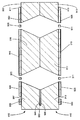
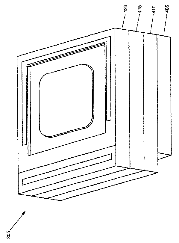
加速度計305は、加速度計を形成するのに適した任意の数の構成要素を含むことができる。図4、図5および図6を参照すると、好ましい実施形態では、加速度計305は頂部キャップ・ウェーハ405、頂部測定質量部分410、底部測定質量部分415、および底部キャップ・ウェーハ420を含む。加速度計305の動作は、ほぼ米国特許第5,852,242号に記載されているように提供することが好ましく、その開示は、参照により本明細書に組み込まれる。
【0021】
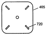
頂部キャップ・ウェーハ405は、頂部キャップ・ウェーハの形成に適し、従来市販されている任意の数の構成要素を含むことができる。好ましい実施形態では、図7a、図7b、図7c、図7d、図7e、図7f、図7g、図7h、図7i、図7j、図7kおよび図7lで示すように、頂部キャップ・ウェーハ405は頂部ウェーハ・キャップ本体406、上面407、底面408、頂部コンデンサ電極705、頂部結合リング707、頂部結合酸化物リング710、頂部キャップ寄生溝715、頂部キャップ過剰衝撃バンパ720、頂部キャップ・プレス・フレームの窪み725、頂部キャップ平衡金属パターン730、頂部キャップ接触パッド735を含む。
【0022】
頂部キャップ・ウェーハ本体406は、例えばガラス、クォーツ、セラミック、またはシリコンなど、キャップ・ウェーハ本体の生成に適し、従来市販されている任意の数の材料から作成することができる。好ましい実施形態では、頂部キャップ・ウェーハ本体406はシリコンで作成する。
【0023】
頂部コンデンサ電極705は、外部回路から電気信号を時間ベースで多重伝送するのに使用することが好ましく、その操作はほぼ、___に出願された米国特許出願第___号、代理人文書第14737.733号に記載された通りであり、その開示は参照により本明細書に組み込まれる。頂部コンデンサ電極705は、頂部キャップ・ウェーハ本体406の底面408で、頂部キャップ寄生溝715によって限定された区間内に位置することが好ましい。好ましい実施形態では、図7cで示すように、頂部コンデンサ電極705はスロット706を含み、この中に頂部キャップ過剰衝撃バンパ720を作成する。頂部コンデンサ電極705は、例えば金属、珪化物またはドーピングした半導体など、電極の生成に適した任意の数の導電材料から作成することができる。好ましい実施形態では、頂部コンデンサ電極705を金とチタンの組合せから作成する。好ましい実施形態では、金とチタンの組合せは、金の層をチタン層の頂部に配置する。チタン層は、シリコンおよび二酸化シリコンへの金の付着を改良することが好ましい。
【0024】
頂部結合リング707および頂部結合酸化物リング710は、頂部キャップ・ウェーハ405を頂部測定質量部分410に結合し、頂部測定質量部分410の上面に配置された電極と頂部コンデンサ電極705の間に狭いギャップを形成するのに役立つことが好ましい。頂部結合酸化物リング710は、頂部キャップ・ウェーハ405と頂部測定質量部分410の間に電気絶縁を提供することが好ましい。頂部結合リング707および頂部結合酸化物リング710は、頂部キャップ・ウェーハ本体406の底面408に配置することが好ましい。頂部結合リング707は、例えば金、銀、またはアルミなど、結合リングの作成に適した任意の数の材料から作成することができる。好ましい実施形態では、頂部結合リング707は金とチタンとの組合せから作成する。好ましい実施形態では、金とチタンの組合せは、金の層をチタンの層の頂部に配置する。チタン層は、シリコンおよび二酸化シリコンへの金の付着を改良することが好ましい。結合リング707は、加速度計305内で使用するのに適した任意の寸法を有することができる。好ましい実施形態では、図7aで示すように、結合リング707は、頂部キャップ・プレス・フレームの窪み725の幅より小さい幅d1を有する。好ましい実施形態では、結合リング707は、頂部キャップ過剰衝撃バンパ720の下で距離d2だけ延在する。頂部結合酸化物リング710は、例えば二酸化シリコンまたは誘電体など、結合酸化物リングの作成に適し、従来市販されている任意の数の材料から作成することができる。好ましい実施形態では、頂部結合酸化物リング710は、二酸化シリコンから作成する。
【0025】
頂部キャップ寄生溝715は、外部閉ループ回路の静電気フィードバックの、頂部測定質量部分410に含まれたばねへの結合を最小にすることが好ましい。頂部キャップ寄生溝715は、頂部キャップ・ウェーハ本体406の底面408にある溝であることが好ましい。頂部キャップ寄生溝715は、頂部コンデンサ電極705を限定し、頂部結合酸化物リング710に囲まれることが好ましい。頂部キャップ寄生溝715は、適切な寄生溝の生成に適した任意の寸法を含むことができる。好ましい実施形態では、頂部キャップ寄生溝715は、寸法が深さ約5μmより大きく、頂部測定質量部分410内にあるばねの幅より広い幅を有する。
【0026】
頂部キャップ過剰衝撃バンパ720は、頂部測定質量部分410に面外衝撃保護を提供することが好ましい。頂部キャップ過剰衝撃バンパ720は、頂部キャップ・ウェーハ本体406の底面408に配置することが好ましく、頂部コンデンサ電極705の切欠き706を通して露出する。頂部キャップ過剰衝撃バンパ720は、例えば二酸化シリコンまたは誘電体など、過剰衝撃バンパの生成に適し、従来市販されている任意の数の材料から作成することができる。好ましい実施形態では、頂部キャップ過剰衝撃バンパ720は二酸化シリコンで作成する。好ましい実施形態では、図7aで示すように、頂部過剰衝撃バンパ720は幅w1を有する。頂部キャップ・ウェーハ405は、任意の数の頂部キャップ過剰衝撃バンパ720を含むことができる。頂部キャップ過剰衝撃バンパ720の設計およびレイアウトは、幾つかの要素の影響を受ける。好ましい実施形態では、頂部キャップ過剰衝撃バンパ720の設計およびレイアウトは、衝撃保護の必要性と、頂部測定質量部分410に配置された金属電極パターン910と頂部キャップ過剰衝撃バンパ720との最小静摩擦の必要性とのバランスをとる。静摩擦は、加速度計305の作動中に、頂部キャップ過剰衝撃バンパ720が頂部測定質量部分410上の金属電極パターン910に付着した場合に発生する。頂部測定質量部分410に配置された金属電極パターンと頂部キャップ過剰衝撃バンパ720との間の静摩擦は、例えば頂部測定質量部分410に配置された金属電極パターン910に頂部キャップ過剰衝撃バンパ720を刻印すること、ファンデルワールス力、静電力、加速度計305の作成の結果生じた表面残滓、またはパッケージから誘発された応力など、幾つかの発生源から生じることがある。好ましい実施形態では、図7dで示すように、頂部キャップ・ウェーハ405は4つのバンパを含む。代替実施形態では、図7eで示すように、頂部キャップ・ウェーハ405は5つの頂部キャップ過剰衝撃バンパ720を含む。代替実施形態では、図7fで示すように、頂部キャップ・ウェーハ405は、幾何学的に配置された8つの頂部キャップ過剰衝撃バンパ720を含む。代替実施形態では、図7gで示すように頂部キャップ・ウェーハ405は、幾何学的に配置された9つの頂部キャップ過剰衝撃バンパ720を含む。代替実施形態では、図7hで示すように、頂部キャップ・ウェーハ405は、3つの平行な直線の列で配置された9つの頂部キャップ過剰衝撃バンパ720を含み、各列が3つのバンパ720を含む。代替実施形態では、図7iで示すように、頂部キャップ・ウェーハ405は、幾何学的に配置された13の頂部キャップ過剰衝撃バンパ720を含む。代替実施形態では、図7jで示すように、頂部キャップ・ウェーハ405は、49の頂部キャップ過剰衝撃バンパ720を含む。代替実施形態では、図7kおよび図7lで示すように、頂部キャップ・ウェーハ405は、円形および隆起状に幾何学的に配置された複数の頂部キャップ過剰衝撃バンパ720を含む。
【0027】
頂部キャップ・プレス・フレームの窪み725は、頂部キャップ・ウェーハ本体406の上面407で、頂部キャップ平衡金属パターン730と頂部キャップ接触パッド735との間に配置することが好ましい。頂部キャップ・プレス・フレーム窪み725は、結合プロセス中に加えられる結合力が頂部結合酸化物リング710の領域に局所化されることを保証することが好ましい。結合力を、頂部コンデンサ電極705と頂部測定質量部分410の上面に配置された電極との間の狭いギャップの領域ではなく、頂部結合酸化物リング710領域に局所化することにより、電極間の狭いギャップが維持される。頂部キャップ・プレス・フレーム窪み725は、例えばシリコン・エッチングなど、プレス・フレーム窪みを形成するのに適した幾つかの処理ステップを使用して形成することができる。好ましい実施形態では、頂部キャップ・プレス・フレーム窪み725を、頂部キャップ・ウェーハ本体406の上面407にエッチングする。頂部キャップ・プレス・フレーム窪み725は、プレス・フレーム窪みの生成に適した任意の寸法を含むことができる。好ましい実施形態では、頂部キャップ・プレス・フレーム窪み725は、寸法が深さ約20μmであり、結合リング707の幅d1より広い幅を有する。
【0028】
頂部キャップ接触パッド735は、頂部キャップ・ウェーハ本体406の上面407に配置することが好ましい。頂部キャップ接触パッド735は、例えば金、アルミ、または銀など、接触パッドの生成に適し、従来市販されている任意の数の材料を含むことができる。好ましい実施形態では、頂部キャップ接触パッド735は金で作成する。別の好ましい実施形態では、頂部キャップ接触パッド735は金とチタンの組合せで作成する。好ましい実施形態では、金とチタンの組合せは、金の層をチタンの層の頂部に配置する。チタン層は、シリコンおよび二酸化シリコンへの金の付着を改良することが好ましい。
【0029】
頂部キャップ平衡金属パターン730は、頂部キャップ・ウェーハ本体406の反りを最小にするために使用する。頂部キャップ・ウェーハ本体406の反りは、加速度計305の性能に悪影響を与えるので望ましくない。頂部キャップ・ウェーハ本体406の反りは、通常、頂部キャップ・ウェーハ本体406と頂部コンデンサ電極705の金属との熱膨張率(TCE)の差から生じる。好ましい実施形態では、頂部キャップ・ウェーハ本体406の材料はシリコンである。好ましい実施形態では、頂部キャップ平衡金属パターン730は、パターンおよび厚さが頂部コンデンサ電極705とほぼ等しく、頂部キャップ・プレス・フレーム窪み725の内部で、頂部コンデンサ電極705のほぼ反対側に配置される。好ましい実施形態では、頂部キャップ平衡金属パターン730は、頂部コンデンサ電極705の切欠き705をオフセットする切欠き731を含む。この位置合わせは、TCEの不一致が加速度計305の性能に与える影響を最小に抑えるのに役立つ平衡した金属/シリコン/金属のサンドイッチを生成することが好ましい。
【0030】
底部キャップ・ウェーハ420は、底部キャップ・ウェーハの形成に適し、従来市販されている任意の数の構成要素を含むことができる。好ましい実施形態では、図8a、図8bおよび図8cで示すように、底部キャップ・ウェーハ420は底部キャップ・ウェーハ本体421、上面423、底面422、底部コンデンサ電極805、底部結合リング807、底部結合酸化物リング810、底部キャップ寄生溝815、底部キャップ過剰衝撃バンパ820、底部キャップ・プレス・フレーム窪み825、底部キャップ平衡金属パターン830、底部キャップ接触パッド835、および延長キャップはんだ取付け(ECSA)金属結合パッド840を含む。
【0031】
底部キャップ・ウェーハ本体421は、例えばガラス、クォーツ、セラミックまたはシリコンなど、キャップ・ウェーハ本体の生成に適し、従来市販されている任意の数の材料から作成することができる。好ましい実施形態では、底部キャップ・ウェーハ本体421はシリコンで作成する。
【0032】
底部コンデンサ電極805は、外部回路からの電気信号を時間ベースで多重伝送するのに使用することが好ましく、その操作はほぼ、___に出願された米国特許出願第___号、代理人文書番号第14747.733号に記載された通りであり、その開示は参照により本明細書に組み込まれる。底部コンデンサ電極805は、底部キャップ・ウェーハ本体421の上面で、底部キャップ寄生溝815に限定された区域内に配置することが好ましい。好ましい実施形態では、図8cで示すように、底部コンデンサ電極805は、底部キャップ過剰衝撃バンパ820が内部に形成される切欠き806を含む。底部コンデンサ電極805は、例えば金属、珪化物またはドーピングした半導体など、電極の生成に適した任意の数の導体材料を使用して作成することができる。好ましい実施形態では、底部コンデンサ電極805は、金とチタンの組合せから作成する。好ましい実施形態では、金とチタンの組合せは、金の層をチタンの層の頂部に配置する。チタン層は、シリコンおよび二酸化シリコンへの金の付着を改良することが好ましい。
【0033】
底部結合リング807および底部結合酸化物リング810は、底部キャップ・ウェーハ420を底部測定質量部分415に結合することが好ましく、底部コンデンサ電極805と底部測定質量部分415の下面に配置された電極との間に狭いギャップを確立するのに役立つ。底部結合酸化物リング810は、底部キャップ・ウェーハ420と底部測定質量部分415との間に電気絶縁を提供することが好ましい。底部結合リング807および底部結合酸化物リング810は、底部キャップ・ウェーハ本体421の上面423に配置することが好ましい。底部結合リング807は、例えばアルミ、銀または金など、結合リングの作成に適した任意の数の材料から作成することができる。好ましい実施形態では、底部結合リング807は、金とチタンの組合せから作成する。好ましい実施形態では、金とチタンの組合せは、金の層をチタンの層の頂部に配置する。チタンの層は、シリコンおよび二酸化シリコンへの金の付着を改良することが好ましい。好ましい実施形態では、結合リング807は、底部キャップ・プレス・フレーム窪み825の幅より小さい幅d4を有する。好ましい実施形態では、結合リング807は底部キャップ過剰衝撃バンパ820を越えて距離d3だけ延在する。底部結合酸化物リング810は、例えば誘電体など、結合酸化物リングの作成に適し、従来市販されている任意の数の材料を含むことができる。好ましい実施形態では、底部結合酸化物リング810は二酸化シリコンから作成する。
【0034】
底部キャップ寄生溝815は、外部閉ループ回路の静電気フィードバックの、底部測定質量部分415に含まれたばねへの結合を最小にすることが好ましい。底部キャップ寄生溝815は、底部キャップ・ウェーハ本体421の底面423にある溝であることが好ましい。底部キャップ寄生溝815は、底部コンデンサ電極805を限定し、底部結合酸化物リング810に囲まれることが好ましい。底部キャップ寄生溝815は、適切な寄生溝の生成に適した任意の寸法を含むことができる。好ましい実施形態では、底部キャップ寄生溝815は、寸法が深さ約5μmより大きく、底部測定質量部分415内にあるばねの幅より広い幅を有する。
【0035】
底部キャップ過剰衝撃バンパ820は、底部測定質量部分415に面外衝撃保護を提供することが好ましい。底部キャップ過剰衝撃バンパ820は、底部キャップ・ウェーハ本体406の上面423に配置することが好ましく、底部コンデンサ電極805の切欠き806を通して露出する。底部キャップ過剰衝撃バンパ820は、例えば誘電体または二酸化シリコンなど、過剰衝撃バンパの生成に適し、従来市販されている任意の数の材料から作成することができる。好ましい実施形態では、底部キャップ過剰衝撃バンパ820は二酸化シリコンで作成する。好ましい実施形態では、底部キャップ過剰衝撃バンパ820は幅w2を有する。底部キャップ・ウェーハ420は、任意の数の底部キャップ過剰衝撃バンパ820を含むことができる。底部キャップ過剰衝撃バンパ820の設計およびレイアウトは、幾つかの要素の影響を受ける。好ましい実施形態では、底部キャップ過剰衝撃バンパ820の設計およびレイアウトは、衝撃保護の必要性と、底部測定質量部分415に配置された金属電極パターン915と底部キャップ過剰衝撃バンパ820との最小静摩擦の必要性とのバランスをとる。静摩擦は、加速度計305の作動中に、底部キャップ過剰衝撃バンパ820が底部測定質量部分415上の金属電極パターン915に付着した場合に発生する。底部測定質量部分415に配置された金属電極パターンと底部キャップ過剰衝撃バンパ820との間の静摩擦は、例えば底部測定質量部分415に配置された金属電極パターン915に底部キャップ過剰衝撃バンパ820を刻印すること、ファンデルワールス力、静電力、加速度計305の作成の結果生じた表面残滓、またはパッケージから誘発された応力など、幾つかの発生源から生じることがある。好ましい実施形態では、底部キャップ・ウェーハ420上の底部キャップ過剰衝撃バンパ820の数は、頂部キャップ・ウェーハ405上の頂部キャップ過剰衝撃バンパ720の数と等しく、その変形を図7d、図7e、図7f、図7g、図7h、図7i、図7j、図7kおよび図7lに示す。
【0036】
底部キャップ・プレス・フレームの窪み825は、底部キャップ・ウェーハ本体421の底面422で、底部キャップ平衡金属パターン830と底面422の外縁との間に配置することが好ましい。底部キャップ・プレス・フレーム窪み825は、結合プロセス中に加えられる結合力が底部結合酸化物リング810の領域に局所化されることを保証することが好ましい。結合力を、底部コンデンサ電極805と底部測定質量部分415の底面に配置された電極との間の狭いギャップの領域ではなく、底部結合酸化物リング810領域に局所化することにより、電極間の狭いギャップが維持される。底部キャップ・プレス・フレーム窪み825は、例えばシリコン・エッチングなど、プレス・フレーム窪みを形成するのに適した幾つかの処理ステップを使用して形成することができる。好ましい実施形態では、底部キャップ・プレス・フレーム窪み825を、底部キャップ・ウェーハ本体421の底面422にエッチングする。底部キャップ・プレス・フレーム窪み825は、プレス・フレーム窪みの生成に適した任意の寸法を含むことができる。好ましい実施形態では、底部キャップ・プレス・フレーム窪み825は、寸法が高さ約20μmより大きく、結合リング807の幅d4より広い幅を有する。
【0037】
底部キャップ接触パッド835は、底部キャップ・ウェーハ本体421の底面422に配置することが好ましい。底部キャップ接触パッド835は、ウェーハのプロービングに使用可能であることが好ましい。底部キャップ接触パッド835は、例えば金、アルミ、または銀など、接触パッドの生成に適し、従来市販されている任意の数の材料を含むことができる。好ましい実施形態では、底部キャップ接触パッド835は金とチタンの組合せで作成する。好ましい実施形態では、金とチタンの組合せは、金の層をチタンの層の頂部に配置する。チタン層は、シリコンおよび二酸化シリコンへの金の付着を改良することが好ましい。
【0038】
底部キャップ平衡金属パターン830は、底部キャップ・ウェーハ本体421の反りを最小にするために使用する。底部キャップ・ウェーハ本体421の反りは、加速度計305の性能に悪影響を与えるので望ましくない。底部キャップ・ウェーハ本体421の反りは、通常、底部キャップ・ウェーハ本体421を構成する材料と底部コンデンサ電極805の金属との熱膨張率(TCE)の差から生じる。好ましい実施形態では、底部キャップ・ウェーハ本体406を構成する材料はシリコンである。好ましい実施形態では、底部キャップ平衡金属パターン830は、パターンおよび厚さが底部コンデンサ電極805とほぼ等しく、底部キャップ・プレス・フレーム窪み825の内部で、底部コンデンサ電極805のほぼ反対側に配置される。図8bで示すように、底部キャップ平衡金属パターン830は、底部コンデンサ電極805の切欠き8065をオフセットするよう設計された切欠き831を含むことが好ましい。この位置合わせは、TCEの不一致が加速度計305の性能に与える影響を最小に抑えるのに役立つ平衡した金属/シリコン/金属のサンドイッチを生成することが好ましい。
【0039】
ECSA金属結合パッド840は、加速度計305が配置される外部パッケージに導電性ダイ接着するのに使用可能であることが好ましい。ECSA金属結合パッド840の操作はほぼ、___に出願された米国特許出願第___号、代理人文書第14737.733号に記載された通りであり、その開示は参照により本明細書に組み込まれる。
【0040】
頂部測定質量部分410は、測定質量部分の生成に適し、従来市販されている任意の数の材料を含むことができる。好ましい実施形態では、図9a、図9aa、図9ac、図9ad、図9b、図9cおよび図9dで示すように、頂部測定質量部分410は、上面411、下面412、1つまたは複数のばね905、結合リング920、および頂部質量接触パッド930を含む。別の好ましい実施形態では、頂部測定質量部分410は、さらに、溝940を含む。
【0041】
ばね905は、頂部測定質量906をハウジング907に結合し、頂部測定質量906とハウジング907との間に導電路を提供することが好ましい。ばね905は、例えばクォーツ、金属またはシリコンなど、ばねを生成するのに適し、従来市販されている任意の数の材料から作成することができる。好ましい実施形態では、ばね905はシリコンで作成し、頂部測定質量版部410のウェーハからミクロ機械加工する。ばね911は、頂部測定質量906に横方向の衝撃保護を提供しながら、交叉軸阻止を維持するよう設計することが好ましい。ばね905は直線のL字形ばねであることが好ましく、その設計は米国特許第5,652,384号および第5,777,226号に記載され、その開示は参照により本明細書に組み込まれる。
【0042】
頂部測定質量906は、測定データの検出に使用する。頂部測定質量906は、その使用が適切な任意の用途に使用することができる。好ましい実施形態では、頂部測定質量906は、地震用途に使用して加速度を検出する。頂部測定質量906は、ばね905によってハウジング907と結合することが好ましい。頂部測定質量906は、例えば金属、クォーツまたはシリコンなど、測定質量の生成に適し、従来市販されている任意の数の材料から作成することができる。好ましい実施形態では、頂部測定質量906はシリコンで作成し、頂部測定質量部分410のウェーハからミクロ機械加工する。
【0043】
ハウジング907は頂部測定質量906を囲み、ばね906によって頂部測定質量906に結合される。ハウジング907は、例えば金属、クォーツまたはシリコンなど、ハウジングの生成に適し、従来市販されている任意の数の材料から作成することができる。好ましい実施形態では、ハウジング907はシリコンから作成し、頂部測定質量部分410のウェーハからミクロ機械加工する。
【0044】
金属電極パターン910は、外部回路からの電気信号の時間ベースの多重伝送に使用する。好ましい実施形態では、金属電極パターン910は1本の電極を含む。好ましい実施形態では、金属電極パターン910は頂部測定質量部分410の上面411で、頂部測定質量906の上に配置される。金属電極パターン910は、例えばアルミ、銀または金など、電極パターンの生成に適し、従来市販されている任意の数の材料を含むことができる。好ましい実施形態では、金属電極パターン910は、金とチタンの組合せから作成する。好ましい実施形態では、金とチタンの組合せは、金の層をチタンの層の頂部に配置する。チタン層は、シリコンおよび二酸化シリコンへの金の付着を改良することが好ましい。金属電極パターン910は、例えば円形、正方形または長方形など、電極パターンを形成するのに適した任意のサイズまたは形状でよい。金属電極パターン910は、頂部コンデンサ電極705とサイズおよび形状がほぼ等しいことが好ましい。代替実施形態では、金属電極パターン910は、結合リング920とほぼ等しい厚さである。好ましい実施形態では、金属電極パターン910および結合リングの厚さは、頂部結合リング707の厚さより小さい。金属電極パターン910と結合リング920と頂部結合リング707との厚さの差は、加速度計305の作動中に、金属電極パターン910への頂部キャップ過剰衝撃バンパ720の刻印を減少させることにより、頂部キャップ過剰衝撃バンパ720と金属電極パターン910間の静摩擦を軽減することが好ましい。別の好ましい実施形態では、図9aaで示すように、金属電極パターン910は、加速度計305の作動中に頂部キャップ過剰衝撃バンパ720と金属電極パターン910との間の静摩擦を最小に抑えるよう設計された1つまたは複数のパターン960aを含む。パターン960aは、加速度計305内の静摩擦を軽減するのに適した任意の形状を含むことができる。金属電極パターン910内のパターン960aは、頂部キャップ過剰衝撃バンパ720と金属電極パターン910との間の密接な接触領域の表面積を最小に抑えることにより、頂部キャップ過剰衝撃バンパ720と金属電極パターン910との間の静摩擦を軽減することが好ましい。別の好ましい実施形態では、図9acで示すように、金属電極パターン910は、頂部キャップ過剰衝撃バンパ720が金属電極パターン910と接触する区域に1つまたは複数の厚さが減少した窪み970aを含む。金属電極パターン910内の厚さが減少した窪み970aは、頂部キャップ過剰衝撃バンパ720と金属電極パターン910との間の静摩擦を軽減するよう設計することが好ましい。厚さが減少した窪み970aは、金属電極パターン910に厚さが減少した窪みを形成するのに適した任意の方法を使用して形成することができる。好ましい実施形態では、厚さが減少した窪み970aは、金属電極パターン910から金の層を除去し、下にあるチタン層を露出させることによって形成する。厚さが減少した窪み970aは、加速度計305内の静摩擦を軽減するのに適した任意の形状を有することができる。好ましい実施形態では、厚さが減少した窪み970aは、頂部キャップ過剰衝撃バンパ720の幅w1より広く、金属電極パターン910上で、頂部キャップ過剰衝撃バンパ720が金属電極パターン910と接触区域に配置される。金属電極パターン910の厚さが減少した窪み970aは、頂部キャップ過剰衝撃バンパ720が金属電極パターン910と接触した場合に発生する金属電極パターン910の刻印の量を減少させることにより、頂部キャップ過剰衝撃バンパ720と金属電極パターン910との間の静摩擦を軽減することが好ましい。別の好ましい実施形態では、図9adで示すように、金属電極パターン910は1つまたは複数の空洞980aを含む。金属電極パターン910の空洞980aは、頂部キャップ過剰衝撃バンパ720と金属電極パターン910との間の静摩擦を解消するよう設計することが好ましい。空洞980aは、金属電極パターン910に空洞を形成するのに適した任意の方法を使用して形成することができる。好ましい実施形態では、空洞980aは、金層およびチタン層を金属電極パターン910から選択的に除去し、下にある頂部測定質量部分410を露出させることによって形成する。空洞980aは、加速度計305内の静摩擦を軽減するのに適した任意の形状を有することができる。好ましい実施形態では、空洞980aは、頂部過剰衝撃バンパ720の幅w1より広く、金属電極パターン910上で、頂部キャップ過剰衝撃バンパ720が金属電極パターン910と接触する区域に配置される。金属電極パターン910の空洞980aは、頂部キャップ過剰衝撃バンパ720が金属電極パターン910と接触した場合に発生する金属電極パターン910の刻印を解消することにより、頂部キャップ過剰衝撃バンパ720と金属電極パターン910との間の静摩擦を軽減することが好ましい。金属電極パターン910の操作はほぼ、___に出願された米国特許出願第___号、代理人文書第14737.733号に記載された通りであり、その開示は参照により本明細書に組み込まれる。
【0045】
結合リング920は、頂部測定質量部分410の頂部キャップ・ウェーハ405への結合を容易にする。結合リング920は、例えば金、アルミまたは銀など、結合リングの生成に適し、従来市販されている任意の数の材料を含むことができる。好ましい実施形態では、結合リング920は金とチタンの組合せから作成する。好ましい実施形態では、金とチタンの組合せは、金の層をチタンの層の頂部に配置する。チタン層は、シリコンおよび二酸化シリコンへの金の付着を改良することが好ましい。結合リング920は、頂部測定質量部分410の上面411で、ハウジング907の内縁に隣接して配置することが好ましい。
【0046】
頂部質量接触パッド930は、頂部測定質量部分410との電気的接触を形成するために使用することが好ましい。頂部質量接触パッド930は、ハウジング907の上面411のいずこかに配置することができる。好ましい実施形態では、頂部質量接触パッド930は、ハウジング907の上面411の、金属電極パターン910から離れた外縁に配置される。頂部質量接触パッド930は、例えば銀、アルミまたは金など、接触パッドの生成に適した任意の材料から作成することができる。好ましい実施形態では、頂部接触パッド930はは金とチタンの組合せで作成する。好ましい実施形態では、金とチタンの組合せは、金の層をチタンの層の頂部に配置する。チタン層は、シリコンおよび二酸化シリコンへの金の付着を改良することが好ましい。頂部質量接触パッド930は、接触パッドの生成に適した任意の寸法を含んでよい。好ましい実施形態では、頂部質量接触パッド930は、従来のワイヤ・ボンディングが可能なほど十分に大きい。
【0047】
溝940は、ハウジング907の下面412に配置され、ハウジング907の外縁からハウジング907の内縁へと延在することが好ましい。溝940は、頂部測定質量部分410を底部測定質量部分415に結合した場合に、通路950を形成することが好ましい。通路950は、加速度計305内の空洞から空気を除去し、加速度計305を真空パッケージ内で密封した場合に、加速度計305内に真空または低圧環境を生成することが好ましい。溝940は、通気用の通路を生成するのに適した任意の方法で形成してよい。好ましい実施形態では、溝940はV字形である。好ましい実施形態では、溝940は、真空へとポンプで空気抜きする間に、加速度計305内から空気の流体が流出できるよう設計する。頂部測定質量部分410は、任意の数の溝940を含んでよい。好ましい実施形態では、頂部測定質量部分410は2本の溝940を含む。代替実施形態では、頂部測定質量部分410は複数の溝940を含む。代替実施形態では、頂部測定質量部分410は溝940を含まない。溝940の形状は、幾つかの要素の影響を受ける。好ましい実施形態では、溝940は、通路950を通過する空気の最適ポンプ空気抜き時間を達成するよう設計する。通路950を通る空気のコンダクタンスは、下式で与えることが好ましい。
【数1】
C=通路950のコンダクタンス、
k=ボルツマン定数、
T=絶対温度、
m=気体原子の質量
A=通路950の断面積、
B=通路950の断面積の周長、および
L=通路950の長さである。
【0048】
長さL、断面積Aおよび周長Bなど、通路950の寸法は、通路950を通る空気のコンダクタンスを最適にするよう設計することが好ましい。好ましい実施形態では、通路950の最適コンダクタンスCは、加速度計305内から空気を除去する最適ポンプ空気抜き時間を生じる。ポンプ空気抜き時間は、加速度計305内に所望の圧力を達成するために、加速度計305内から十分な空気を除去するのにかかる時間の量である。ポンプ空気抜き時間は、下式で与えることが好ましい。
【数2】
t=ポンプ空気抜き時間、
V=加速度計305内の内部空洞の容積、
S=加速度計305から空気を除去するために使用する真空ポンプの速度、
C=式(1)からの通路950のコンダクタンス、
Pi=加速度計305内の初期圧力(通常は1気圧)、
P=加速度計305内の所望の圧力、
Pu=(1+S/C)*Po、および
Po=ポンプの最低圧力である。
【0049】
底部測定質量部分415は、測定部分の生成に適し、従来市販されている任意の数の材料から作成することができる。好ましい実施形態では、図9a、図9ab、図9ac、図9ad、図9e、図9fおよび図9gで示すように、底部測定質量部分415は、上面417、下面416、1つまたは複数のばね911、底部測定質量912、ハウジング913、金属電極パターン915、結合リング925、底部質量接触パッド935、および溝945を含む。
【0050】
ばね911は、底部測定質量912をハウジング913に結合し、底部測定質量912とハウジング913との間に導電路を提供することが好ましい。ばね911は、例えば金属、クォーツ、ポリシリコンまたはシリコンなど、ばねを生成するのに適し、従来市販されている任意の数の材料から作成することができる。好ましい実施形態では、ばね911はシリコンで作成し、底部測定質量版部415のウェーハからミクロ機械加工する。ばね911は、底部測定質量912に横方向の衝撃保護を提供しながら、交叉軸阻止を維持するよう設計することが好ましい。ばね911は直線のL字形ばねであることが好ましく、その設計は米国特許第5,652,384号および第5,777,226号に記載され、その開示は参照により本明細書に組み込まれる。
【0051】
底部測定質量912は、測定データの検出に使用する。底部測定質量912は、その使用が適切な任意の用途に使用することができる。好ましい実施形態では、底部測定質量912は、地震用途に使用して加速度を検出する。底部測定質量912は、ばね911によってハウジング913と結合することが好ましい。底部測定質量912は、例えばシリコンまたはクォーツなど、測定質量の生成に適した任意の材料から作成することができる。好ましい実施形態では、底部測定質量912はシリコンで作成し、底部測定質量部分415のウェーハからミクロ機械加工する。
【0052】
ハウジング913は底部測定質量912を囲み、ばね911によって底部測定質量912に結合される。ハウジング913は、例えばクォーツまたはシリコンなど、ハウジングの生成に適した任意の材料から作成することができる。好ましい実施形態では、ハウジング913はシリコンから作成し、底部測定質量部分415のウェーハからミクロ機械加工する。
【0053】
金属電極パターン915は、外部回路からの電気信号の時間ベースの多重伝送に使用する。好ましい実施形態では、金属電極パターン915は1本の電極を含む。好ましい実施形態では、金属電極パターン915は底部測定質量部分415の下面416で、底部測定質量912の表面に配置される。金属電極パターン915は、例えば銀、アルミまたは金など、電極パターンの生成に適し、従来市販されている任意の数の材料を含むことができる。好ましい実施形態では、金属電極パターン915は、金とチタンの組合せから作成する。好ましい実施形態では、金とチタンの組合せは、金の層をチタンの層の頂部に配置する。チタン層は、シリコンおよび二酸化シリコンへの金の付着を改良することが好ましい。金属電極パターン915は、例えば円形、正方形または長方形など、電極パターンを形成するのに適した任意のサイズまたは形状でよい。金属電極パターン915は、底部コンデンサ電極805とサイズおよび形状がほぼ等しいことが好ましい。好ましい実施形態では、金属電極パターン915は、結合リング925とほぼ等しい厚さである。好ましい実施形態では、金属電極パターン915および結合リング925の厚さは、底部結合リング807の厚さより小さい。金属電極パターン915と結合リング925と底部結合リング807との厚さの差は、加速度計305の作動中に、金属電極パターン915への底部キャップ過剰衝撃バンパ820の刻印を減少させることにより底部キャップ過剰衝撃バンパ820と金属電極パターン915間の静摩擦を軽減することが好ましい。別の好ましい実施形態では、図9abで示すように、金属電極パターン915は、加速度計305の作動中に底部キャップ過剰衝撃バンパ820と金属電極パターン915との間の静摩擦を最小に抑えるよう設計された1つまたは複数のパターン960bを含む。金属電極パターン915内のパターン960bは、底部キャップ過剰衝撃バンパ820と金属電極パターン915との間の密接な接触領域の表面積を最小に抑えることにより、底部キャップ過剰衝撃バンパ820と金属電極パターン915との間の静摩擦を軽減することが好ましい。別の好ましい実施形態では、図9acで示すように、金属電極パターン915は、底部キャップ過剰衝撃バンパ820が金属電極パターン915と接触する区域に1つまたは複数の厚さが減少した窪み970bを含む。金属電極パターン915内の厚さが減少した窪み970bは、底部キャップ過剰衝撃バンパ820と金属電極パターン915との間の静摩擦を軽減するよう設計することが好ましい。厚さが減少した窪み970bは、金属電極パターン915に厚さが減少した窪みを形成するのに適した任意の方法を使用して形成することができる。好ましい実施形態では、厚さが減少した窪み970bは、金属電極パターン915から金の層を除去し、下にあるチタン層を露出させることによって形成する。厚さが減少した窪み970bは、加速度計305内の静摩擦を軽減するのに適した任意の形状を有することができる。好ましい実施形態では、厚さが減少した窪み970bは、底部キャップ過剰衝撃バンパ820の幅w2より広く、金属電極パターン915上で、底部キャップ過剰衝撃バンパ820が金属電極パターン915と接触区域に配置される。厚さが減少した窪み970bは、底部キャップ過剰衝撃バンパ820が金属電極パターン915と接触した場合に発生する金属電極パターン915の刻印の量を減少させることにより、底部キャップ過剰衝撃バンパ820と金属電極パターン915との間の静摩擦を軽減することが好ましい。別の好ましい実施形態では、図9adで示すように、金属電極パターン915は1つまたは複数の空洞980bを含む。金属電極パターン915の空洞980bは、底部キャップ過剰衝撃バンパ820と金属電極パターン915との間の静摩擦を解消するよう設計することが好ましい。空洞980bは、金属電極パターン915に空洞を形成するのに適した任意の方法を使用して形成することができる。好ましい実施形態では、空洞980bは、金層およびチタン層を金属電極パターン915から選択的に除去し、下にある底部測定質量部分415を露出させることによって形成する。空洞980bは、加速度計305内の静摩擦を軽減するのに適した任意の形状を有することができる。好ましい実施形態では、空洞980bは、底部過剰衝撃バンパ820の幅w2より広く、金属電極パターン915上で、底部キャップ過剰衝撃バンパ820が金属電極パターン915と接触する区域に配置される。空洞980bは、底部キャップ過剰衝撃バンパ820が金属電極パターン915と接触した場合に発生する金属電極パターン915の刻印を解消することにより、底部キャップ過剰衝撃バンパ820と金属電極パターン915との間の静摩擦を軽減することが好ましい。金属電極パターン915の操作はほぼ、___に出願された米国特許出願第___号、代理人文書第14737.733号に記載された通りであり、その開示は参照により本明細書に組み込まれる。
【0054】
結合リング925は、底部測定質量部分415の底部キャップ・ウェーハ420への結合を容易にすることが好ましい。結合リング925は、例えば金、アルミまたは銀など、結合リングの生成に適し、従来市販されている任意の数の材料を含むことができる。好ましい実施形態では、結合リング925は金とチタンの組合せから作成する。好ましい実施形態では、金とチタンの組合せは、金の層をチタンの層の頂部に配置する。チタン層は、シリコンおよび二酸化シリコンへの金の付着を改良することが好ましい。結合リング925は、底部測定質量部分415の下面416で、ハウジング913の内縁に隣接して配置することが好ましい。
【0055】
底部質量接触パッド935は、底部測定質量部分415との電気的接触を形成するために使用することが好ましい。底部質量接触パッド935は、ハウジング913の下面416のいずこかに配置することができる。好ましい実施形態では、底部質量接触パッド935は、ハウジング913の下面416の、金属電極パターン915から離れた外縁に配置される。底部質量接触パッド935は、例えばアルミ、銀または金など、接触パッドの生成に適し、従来市販されている任意の数の材料から作成することができる。好ましい実施形態では、底部接触パッド935は金とチタンの組合せで作成する。好ましい実施形態では、金とチタンの組合せは、金の層をチタンの層の頂部に配置する。チタン層は、シリコンおよび二酸化シリコンへの金の付着を改良することが好ましい。底部質量接触パッド935は、接触パッドの生成に適した任意の寸法を含んでよい。好ましい実施形態では、底部質量接触パッド935は、従来のワイヤ・ボンディングが可能なほど十分に大きい。
【0056】
溝945は、底部測定質量部分415を頂部測定質量部分410に結合した場合に、通路950を形成することが好ましい。通路950は、加速度計305内の空洞から空気を除去し、加速度計305を真空パッケージ内で密封した場合に、加速度計305内に真空または低圧環境を生成することが好ましい。溝945は、通気用の通路を生成するのに適した任意の方法で形成してよい。好ましい実施形態では、溝945はV字形である。好ましい実施形態では、溝945は、真空へとポンプで空気抜きする間に、加速度計305内から空気の流体が流出できるよう設計する。溝945の形状は、上述したような溝940の形状とほぼ等しいことが好ましい。溝945は、ハウジング913の上面417に配置され、ハウジング913の外縁からハウジング913の内縁へと延在することが好ましい。底部測定質量部分415は、任意の数の溝945を含んでよい。好ましい実施形態では、底測定質量部分415は2本の溝945を含む。代替実施形態では、底部測定質量部分415は1本の溝945を含む。代替実施形態では、底部測定質量部分415は複数の溝945を含む。代替実施形態では、底部測定質量部分415は溝945を含まない。
【0057】
次に、図10、図11a、図11b、図11c、図11d、図11e、図11f、図11g、図11h、図11ha、図11hb、図11hc、図11hd、図11he、図11hf、図11hg、図11hh、図11hi、図11hj、図11i、図11j、図12a、図12b、図12cおよび図13を参照し、加速度計305の作成方法1000について説明する。好ましい実施形態では、加速度計305を作成する方法1000は、ステップ1005で2枚の開始キャップ・ウェーハを取得し、ステップ1010でキャップ・ウェーハ・プロセスを使用して2枚の開始ウェーハを形成し、ステップ1020で2枚の開始質量ウェーハを取得し、ステップ1025で質量ウェーハ・プロセスを使用して2枚の開始質量ウェーハを形成し、ステップ1035で結合プロセスを使用してウェーハを結合して加速度計305を形成し、ステップ1040で加速度計305上に方形切断カットを作成し、ステップ1045で加速度計305をパッケージングすることを含む。
【0058】
図11aで示すように、ステップ1005で、2枚の開始キャップ・ウェーハ1105aおよび1105bを作成する。好ましい実施形態では、2枚の開始キャップ・ウェーハ1105aおよび1105bは等しいサイズおよび形状である。開始キャップ・ウェーハ1105aおよび1105bは、従来市販されている任意の数の材料から作成することができる。好ましい実施形態では、開始キャップ・ウェーハ1105aおよび1105bはシリコンで作成する。
【0059】
図11bで示すように、ステップ1010では2枚の開始キャップ・ウェーハ1105aおよび1105bはキャップ・ウェーハ・プロセスにかけられる。好ましい実施形態では、キャップ・ウェーハ・プロセスは、開始キャップ・ウェーハ1105aおよび1105bを、それぞれ頂部キャップ・ウェーハ405および底部キャップ・ウェーハ420に変換する。代替実施形態では、キャップ・ウェーハ・プロセスは、以下の1つまたは複数でほぼ開示されているような統合マスク・ミクロ機械加工プロセスを含む。つまり1999年7月13日出願の米国特許出願第09/352,835号、代理人文書第14737,659.02号、1999年7月13日出願の米国特許第09/352,025号、代理人文書第14737.659.03号であり、その開示は参照により本明細書に組み込まれる。
【0060】
図11cで示すように、ステップ1020では、2枚の開始質量ウェーハ1120aおよび1120bを作成する。好ましい実施形態では、2枚の開始質量ウェーハ1120aおよび1120bは等しいサイズおよび形状である。開始質量ウェーハ1120aおよび1120bは、従来市販されている任意の数の材料から作成することができる。好ましい実施形態では、開始質量ウェーハ1120aおよび1120bはシリコンで作成する。好ましい実施形態では、開始質量ウェーハ1120aおよび1120bはそれぞれ、エッチング停止層1140aおよび1140bを含む。好ましい実施形態では、開始質量ウェーハ1120aおよび1120bはそれぞれ、エッチ・マスキング層1150aおよび1150bを含む。
【0061】
図11d、図11e、図11f、図11g、図11h、図11ha、図11hb、図11hc、図11hd、図11he、図11hf、図11hg、図11hh、図11hi、図11hjおよび図11iで示すように、ステップ1025では2枚の開始質量ウェーハ1120aおよび1120bは、2枚の開始質量ウェーハ1120aおよび1120bをそれぞれ頂部測定質量部分410および底部測定質量部分415に変換する質量ウェーハ・プロセスにかけられる。好ましい実施形態では、質量ウェーハ・プロセスは、ほぼ米国特許第5,484,073号に記載された通りであり、その開示は参照により本明細書に組み込まれる。代替実施形態では、質量ウェーハ・プロセスは、1999年7月13日出願の米国特許出願第09/352,835号、代理人文書第14737,659.02号、1999年7月13日出願の米国特許第09/352,025号、代理人文書第14737.659.03号でほぼ開示されたような統合マスク・ミクロ機械加工プロセスを含み、その開示は参照により本明細書に組み込まれる。
【0062】
図11dで示すように、ステップ1025の質量ウェーハ・プロセスは、エッチ・マスキング層1150aをフォトリソグラフィでパターン形成し、エッチ・マスキング層1150aに露出区域1160を生成することによって開始する。好ましい実施形態では、エッチ・マスキング層1150aをフォトリソグラフィでパターン形成し、頂部即知恵質量906、ハウジング907、および溝940の形状の露出区域1160を生成する。好ましい実施形態では、フォトリソグラフィでパターン形成した露出区域1160は、隅補償構造XおよびYを含む。
【0063】
好ましい実施形態では、図11eで示すように、エッチング・プロセスを実行して、開始質量ウェーハ1120aを頂部測定質量部分410に形成する。エッチング・プロセスは、エッチングに適した従来市販されている任意の数のプロセスを含むことができる。好ましい実施形態では、エッチング・プロセスは、エッチ・マスキング層1150aを露出区域1160内の開始質量ウェーハ1120から除去することによって開始する。エッチ・マスキング層1150aは、例えばプラズマ・エッチングなど、エッチ・マスキング層を除去するのに適した任意のプロセスを使用して除去することができる。好ましい実施形態では、エッチ・マスキング層1150aは、エッチング液を使用することにより、露出区域1160内の開始質量ウェーハ1120aから除去される。好ましい実施形態では、エッチ・マスキング層1150aを除去すると、開始質量ウェーハ1120aを作成する元となる材料が露出する。好ましい実施形態では、開始質量ウェーハ1120aを作成する材料はシリコンである。好ましい実施形態では、隅補償構造Xは、エッチング液が露出区域1160内の凸状隅を攻撃し、腐食するのを防止する。隅構造Yにより、測定質量906およびハウジング907の画定に使用するエッチング・プロセス中に、溝940を同時に形成できることが好ましい。好ましい実施形態では、隅補償構造Yは、溝940と露出区域1160の交点で、エッチング液に誘発された隅の腐食を軽減する。
【0064】
好ましい実施形態では、次にウェット・エッチング用化学物質を、開始質量ウェーハ1120a上に露出したシリコンに塗布する。ウェット・エッチング用化学物質は、シリコンのエッチングに適し、従来市販されている任意の数のウェット・エッチング用化学物質でよい。好ましい実施形態では、ウェット・エッチング用化学物質は水酸化カリウム(KOH)である。KOHは、制御自在にシリコンをエッチングし、開始質量ウェーハ1120aのエッチング停止層1140aで終了することが好ましい。好ましい実施形態では、図11fで示すように、KOHは、開始質量ウェーハ1120aを頂部測定質量406、ハウジング407、および溝940の形状にエッチングする。好ましい実施形態では、エッチング停止層1140aは、ウェット化学エッチング・プロセスが完了した後も、ばね905の背面に残る。代替実施形態では、エッチング停止層1140aはウェット化学エッチング・プロセス中にばね905から除去される。
【0065】
ウェット・エッチング・プロセスの後、開始質量ウェーハ1120a上に残ったエッチ・マスキング層1150aが、標準的なウェット・エッチング液を使用して開始質量ウェーハ1120aから除去される。
【0066】
第2開始質量ウェーハ1120bにも同じエッチング・プロセスを使用して、第2開始質量ウェーハ1120bを底部測定質量部分415に形成することが好ましい。
【0067】
好ましい実施形態では、図11gで示すように、頂部測定質量部分410と底部測定質量部分415とを結合し合わせ、質量ウェーハ対1130を形成する。ウェーハ結合プロセスは、頂部測定質量部分410と底部測定質量部分415とを結合するのに適した任意の数の結合プロセスでよい。好ましい実施形態では、ウェーハ結合プロセスは融着プロセスである。好ましい実施形態では、通路950を形成するウェーハ結合プロセスの間に、頂部測定質量部分410の溝940を底部測定質量部分415の溝945と位置合わせする。
【0068】
好ましい実施形態では、金属層1142を質量ウェーハ対1150の上面に蒸着させ、これは頂部測定質量部分410の上面411と対応する。また、金属層1143を質量ウェーハ対1130の下面に蒸着し、これは底部測定質量部分415の下面416に対応する。金属層1142および1143は、例えばアルミ、銀または金など、金属層の生成に適し、従来市販されている任意の数の材料を含むことができる。好ましい実施形態では、金属層1142および1143は、金とチタンの組合せから作成する。好ましい実施形態では、金とチタンの組合せは、金の層をチタンの層の頂部に配置する。チタン層は、シリコンおよび二酸化シリコンへの金の付着を改良することが好ましい。金属層1142および1143は、エッチ・マスキング層を使用してパターン形成することが好ましい。エッチ・マスキング層は、金属層のパターン形成に適した任意のエッチ・マスキング層でよい。好ましい実施形態では、エッチ・マスキング層はフォトレジストである。金属層1142および1143は、加速度計305内に使用するのに適した任意のパターンに形成することができる。好ましい実施形態では、図11hで示すように、質量ウェーハ対1130の上面にある金属層1142は、金属電極パターン910、結合リング920、および頂部質量接触パッド930に形成する。好ましい実施形態では、図11hで示すように、質量ウェーハ対1130の下面にある金属層1143は、金属電極パターン915、結合リング925、および底部質量接触パッド935を形成する。
【0069】
好ましい実施形態では、図11haで示すように、金属電極パターン910は、加速度計305の作動中に金属電極パターン910と頂部キャップ過剰衝撃バンパ720との間の静摩擦を軽減するよう設計されたパターン960aを含む。好ましい実施形態では、図11hbで示すように、金属電極パターン915は、加速度計305の作動中に金属電極パターン915と底部キャップ過剰衝撃バンパ820との間の静摩擦を軽減するよう設計されたパターン960bを含む。パターン960aおよび960bは、金属電極パターン910および915上にパターンを生成するのに適した任意の数の方法を使用し、金属電極パターン910および915上に生成することができる。好ましい実施形態では、図11haで示すように、パターン960aは、頂部測定質量部分410の上面411にパターンをエッチングして、パターン形成した表面1165aを生成し、金属層1142をパターン形成表面1165a上に蒸着することによって生成される。金属層1142は、パターン960aを含む金属電極910に成形することが好ましい。好ましい実施形態では、図11hbで示すように、パターン960bは、底部測定質量部分415の下面416にパターンをエッチングして、パターン形成した表面1165bを生成し、金属層1143をパターン形成表面1165b上に蒸着することによって生成される。金属層1143は、パターン960bを含む金属電極915に成形することが好ましい。頂部測定質量部分410の上面411にエッチングされたパターン形成表面1165a、および底部測定質量部分415の下面416にエッチングされたパターン形成表面1165bは、金属電極パターン910および915と過剰衝撃保護バンパ720および820それぞれの間の静摩擦を軽減するのに適した任意の数のパターンを含むことができる。好ましい実施形態では、図11hcおよび図11hfで示すように、パターン形成表面1165aおよび1165bは、複数の幾何学的に配置された正方形を含む。別の好ましい実施形態では、図11hdおよび図11hgで示すように、パターン形成表面1165aおよび1165bは複数の幾何学的に配置された円形を含む。別の好ましい実施形態では、図11heで示すように、パターン形成表面1165aおよび1165bは、一連の同心円を含む。別の好ましい実施形態では、図11hhで示すように、パターン形成表面1165aおよび1165bは一連の幾何学的に配置された長方形を含む。別の好ましい実施形態では、図11hiおよび図11hjで示すように、パターン形成表面1165aおよび1165bは、一連の幾何学的に配置されたパイ形のセグメントを含む。
【0070】
好ましい実施形態では、図11iで示すように、ばね905は、頂部測定質量906をハウジング907に結合するよう形成され、ばね911は、底部測定質量912をハウジング913に結合するよう形成される。ばね905および911は、質量ウェーハ対1130内にばね部材を生成するのに適し、従来市販されている任意の数の方法を使用して形成することができる。好ましい実施形態では、ばね905および911は、DRIEプラズマ・エッチング技術を使用して形成される。好ましい実施形態では、エッチング技術はほぼ、米国特許第5,484,073号に記載された通りであり、その開示は参照により本明細書に組み込まれる。ばね905および911は、直線のL字形ばねであることが好ましく、その設計は米国特許第5,652,384号および第5,777,226号に記載され、その開示は参照により本明細書に組み込まれる。ばね905および911は、それぞれ頂部測定質量906および底部測定質量912に横方向の衝撃保護を提供しながら、交叉軸阻止を維持するよう設計することが好ましい。好ましい実施形態では、エッチング停止層1140aおよび1140bは、プラズマ・エッチング・プロセスが完了した後も、それぞればね905および911の背面に残る。ばね905および911上のエッチング停止層1140aおよび1140bは、ばね905および911の厚さの均一性を改良することが好ましい。また、ばね905および911上のエッチング停止層1140aおよび1140bは、加速度計305の作動中にばね905の寸法制御を改良することが好ましい。別の好ましい実施形態では、エッチング停止層1140aおよび1140bは、プラズマ・エッチング・プロセス中に、それぞればね905および911から除去される。
【0071】
図11jで示すように、ステップ1035では、頂部キャップ・ウェーハ405、底部キャップ・ウェーハ420、および質量ウェーハ対1130が結合プロセスにかけられて、加速度計305を形成することが好ましい。ステップ1035の結合プロセスは、例えば融着、熱圧着、共晶結合、陽極結合またはガラス・フリット結合など、任意の数の結合プロセスでよい。好ましい実施形態では、ステップ1035の結合プロセスは熱圧着結合プロセスである。
【0072】
ステップ1035の結合プロセス中、後部キャップ・ウェーハ405は質量ウェーハ対1130の上面に結合され、これは頂部測定質量部分410の上面411に対応する。好ましい実施形態では、頂部結合リング707は結合リング920と結合し、頂部キャップ・ウェーハ405と頂部測定質量部分410とを結合する。頂部結合リング707と結合リング920は、熱圧着結合プロセスを使用して結合することが好ましい。
【0073】
頂部結合酸化物リング710は、頂部キャップ・ウェーハ本体406の底面408の下に延在することが好ましい。その結果、結合プロセスは、頂部コンデンサ電極705と金属電極パターン910との間に狭いコンデンサ電極ギャップを生成することが好ましい。結合プロセス中、結合力を頂部キャップ・ウェーハ405の上面407に、頂部キャップ・プレス・フレーム窪み725から離して加えることが好ましい。好ましい実施形態では、頂部キャップ・プレス・フレーム窪み725は、結合プロセス中に加えられる結合力が、結合リング領域に局所化され、狭いコンデンサ電極ギャップ領域から離れていることを保証する位置で、頂部キャップ・ウェーハ405の上面407に配置される。
【0074】
これもステップ1035の結合プロセス中に、底部キャップ・ウェーハ420を質量ウェーハ対1130の下面に結合し、これは底部測定質量部分415の下面416に対応する。好ましい実施形態では、底部結合リング807は結合リング925と結合し、底部キャップ・ウェーハ420と底部測定質量部分415とを結合する。底部結合リング807と結合リング925は、熱圧着結合プロセスを使用して結合することが好ましい。
【0075】
底部結合酸化物リング810は、底部キャップ・ウェーハ本体421の上面423の上に延在することが好ましい。その結果、結合プロセスが、底部コンデンサ電極805と金属電極パターン915との間に狭いコンデンサ電極ギャップを生成することが好ましい。結合プロセス中、結合力は、底部キャップ・ウェーハ420の底面422に、底部キャップ・プレス・フレーム窪み825から離して加えることが好ましい。好ましい実施形態では、底部キャップ・プレス・フレーム窪み825は、結合プロセス中に加えられる結合力が、結合リング領域に局所化され、狭いコンデンサ電極ギャップ領域から離れていることを保証する位置で、底部キャップ・ウェーハ420の底面422に配置される。
【0076】
図12a、図12bおよび図12cで示すように、ステップ1040では、加速度計305が方形切断プロセスにかけられる。方形切断カット1205、1210、1215、1220は加速度計305の予め決められた位置に形成することが望ましい。方形切断カット1205、1210、1215、1220は様々な目的を満足する。好ましい実施形態では、方形切断カット1205、1215、1220は、加速度計305のダイをウェーハ1235から分離して、電極910および915から電気リード線を露出させ、電気リード線を分離し、通路950を露出させるよう作成される。別の好ましい実施形態では、方形切断カット1205、1215、1220に加えて方形切断カット1210を作成して、加速度計305のダイをウェーハ1235から分離し、電極910および915から電気リード線を露出させ、電気リード線を分離し、通路950を露出させる。
【0077】
好ましい実施形態では、カット1205を頂部キャップ・ウェーハ405上に作成する。カット1205は、頂部キャップ・ウェーハ本体406を通って垂直に延在し、頂部キャップ・ウェーハ本体406の区間を除去することが好ましい。好ましい実施形態では、カット1205は頂部質量接触パッド930を露出させる。カット1205は、例えばダイアモンド・ブレードのウェーハ用ソーを使用するなど、従来市販されている任意の数の方形切断カットを実行する方法を使用して実行することができる。好ましい実施形態では、カット1205はダイアモンド・ブレードのウェーハ用ソーを使用して作成する。
【0078】
好ましい実施形態では、カット1215は、頂部キャップ・ウェーハ本体406から垂直に延在し、頂部測定質量部分410のハウジング907に入る。カット1215は、カット1215が通路950に到達する前に、ハウジング907内で停止することが好ましい。カット1215は、通路950に到達する前に任意の距離で停止してよい。好ましい実施形態では、カット1215は通路950から約2ミル(5.1×10⁵m)以上離れて停止する。カット1215は、例えばダイアモンド・ブレードのウェーハ用ソーを使用するなど、従来から商業的に入手可能な任意の数の方形切断カットを実行する方法を使用して実行することができる。好ましい実施形態では、カット1215は、例えばダイアモンド・ブレードのウェーハ用ソーを使用して作成する。
【0079】
好ましい実施形態では、カット1220は、底部キャップ・ウェーハ本体421から垂直に延在し、底部測定質量部分415のハウジング913に入る。カット1220は、カット1220が通路950に到達する前に、ハウジング913内で停止することが好ましい。カット1220は、通路950に到達する前に任意の距離で停止してよい。好ましい実施形態では、カット1220は通路950から約2ミル(5.1×10⁵m)以上離れて停止する。カット1220は、例えばダイアモンド・ブレードのウェーハ用ソーを使用するなど、従来から商業的に入手可能な任意の数の方形切断カットを実行する方法を使用して実行することができる。好ましい実施形態では、カット1215は、例えばダイアモンド・ブレードのウェーハ用ソーを使用して作成する。
【0080】
好ましい代替実施形態では、カット1210を底部キャップ・ウェーハ本体421上に作成する。カット1210は、底部キャップ・ウェーハ本体421を通って垂直に延在し、底部キャップ・ウェーハ本体421の区間を除去することが好ましい。好ましい実施形態では、カット1210は底部質量接触パッド935を露出させる。カット1210は、例えばダイアモンド・ブレードのウェーハ用ソーを使用するなど、従来から商業的に入手可能な任意の数の方形切断カットを実行する方法を使用して実行することができる。好ましい実施形態では、カット1210はダイアモンド・ブレードのウェーハ用ソーを使用して作成する。
【0081】
カット1205、1210、1215、1220は個々に実行するか、カット1205、1210、1215、1220を任意の組合せで作成し、特定の用途に最も適した加速度計305の形状を達成することができる。好ましい実施形態では、図12bで示すように、カット1205、1215および1220を加速度計305上で実行する。代替実施形態では、カット1205、1215および1220に加えてカット1210を加速度計305上で実行する。カット1205は、頂部質量接触パッド930を露出することが好ましい。カット1210は、底部質量接触パッド935を露出することが好ましい。カット1215、1220は、通路950を囲むスクライブ・レーン1230を生成することが好ましい。スクライブ・レーン1230を別のダイ1235に取り付けることが好ましい。
【0082】
方形切断プロセス中、スクライブ・レーン1230は加速度計305およびダイ1235に取り付けたままで、加速度計305を気密封止状態に維持するか、スクライブ・レーン1230をスナップ止めして通路950を露出し、加速度計305をダイ1235から分離することができる。好ましい実施形態では、図12cで示すように、スクライブ・レーン1230を除去して通路950を露出し、加速度計305をダイ1235から分離する。露出した通路950は、加速度計305内から空気を除去し、パッケージング中に加速度計305内に真空を生成する流路として使用することが好ましい。
【0083】
図13で示すように、ステップ1045では、加速度計305をパッケージ1305内にパッケージングする。パッケージ1305は、加速度計305を保存するのに適した任意の数のパッケージを含むことができる。好ましい実施形態では、パッケージ1305はハウジングである。別の好ましい実施形態では、パッケージ1305は基板である。
【0084】
ハウジング1305は、加速度計305の保存に適した任意の数のハウジングでよい。好ましい実施形態では、ハウジング1305は本体1310および蓋1315を含む。ハウジング1305は、従来の多層セラミック・パッケージであることが好ましい。
【0085】
加速度計305は、ハウジング1305の本体1310内に配置することが好ましい。加速度計305は、加速度計305をハウジング1305内に固定するのに適した任意の数の方法を使用して、ハウジング1305内に配置することができる。好ましい実施形態では、加速度計305は、ほぼ___に出願された米国特許出願第___号、代理人文書第14737.743号の開示通りのはんだダイ取付けプロセスを使用して、ハウジング1305内に配置し、その開示は参照により本明細書に組み込まれる。
【0086】
次に、蓋1315を本体1310に締め付けて、ハウジング305内で加速度計305を密封することが好ましい。好ましい実施形態では、蓋1315を本体1310に締め付ける前に、真空プロセスを使用してハウジングから空気を除去し、ハウジング1305内に真空または低圧環境を生成する。通路950が露出したら、真空プロセス中に加速度計305内から空気を除去し、ハウジング1305の加速度計305内に真空を生成する。
【0087】
別の好ましい実施形態では、ステップ1035の結合プロセスを真空環境で実行し、結合プロセス中に加速度計305の空洞内に真空を生成する。この実施形態では、通路950を加速度計305の設計から除去することが好ましい。次に、真空密封加速度計305をハウジング1305内に配置し、蓋1315を本体1310に締め付けることにより、ハウジングを密封することが好ましい。
【0088】
本発明の例示的実施形態について図示し、説明してきたが、以上の開示内で広い範囲の改造、変更および置換が想定される。場合によっては、対応して他の機能を使用しない状態で、本発明の幾つかの特徴を使用することができる。したがって、添付の請求の範囲を広く、本発明の範囲に一致する方法で解釈することが適切である。
【図面の簡単な説明】
【図1】 環境データ測定の収集に使用するシステムの実施形態を示す。
【図2】 図1のシステム内で使用するセンサおよびケーブルの実施形態を示す。
【図3a】 図1のセンサ内における加速度計の配置の断面側面図である。
【図3b】 図1のセンサ内における加速度計の配置の断面上面図である。
【図4】 図3aの加速度計の実施形態の上斜視図を示す。
【図5】 図4の加速度計の底斜視図を示す。
【図6】 図4の加速度計の断面図を示す。
【図7a】 図4の加速度計の頂部キャップ・ウェーハの断面図を示す。
【図7b】 図7aの頂部キャップ・ウェーハの上面図を示す。
【図7c】 図7aの頂部キャップ・ウェーハの底面図を示す。
【図7d】 図7aの頂部キャップ・ウェーハ上における過剰衝撃バンパの配置構成の実施形態を示す。
【図7e】 図7dの過剰衝バンパの代替配置構成の実施形態を示す。
【図7f】 図7dの過剰衝撃バンパの代替配置構成の実施形態を示す。
【図7g】 図7dの過剰衝撃バンパの代替配置構成の実施形態を示す。
【図7h】 図7dの過剰衝撃バンパの代替配置構成の実施形態を示す。
【図7i】 図7dの過剰衝撃バンパの代替配置構成の実施形態を示す。
【図7j】 図7dの過剰衝撃バンパの代替配置構成の実施形態を示す。
【図7k】 図7dの過剰衝撃バンパの代替配置構成の実施形態を示す。
【図7l】 図7dの過剰衝撃バンパの代替配置構成の実施形態を示す。
【図8a】 図4の加速度計の底部キャップ・ウェーハの断面図を示す。
【図8b】 図8aの底部キャップ・ウェーハの底面図を示す。
【図8c】 図8aの底部キャップ・ウェーハの上面図を示す。
【図9a】 図4の加速度径の質量ウェーハ対の断面図を示す。
【図9aa】 図6の加速度計内にある頂部キャップ過剰衝撃バンパおよびパターン状金属電極の断面図を示す。
【図9ab】 図6の加速度計内にある底部キャップ過剰衝撃バンパおよびパターン状金属電極の断面図を示す。
【図9ac】 図6の加速度計内にある、厚さが減少した窪みを含む金属電極の実施形態を示す。
【図9ad】 図6の加速度計内にある、空洞を含む金属電極の実施形態を示す。
【図9b】 図9aの質量ウェーハ対の頂部質量部分の上面図である。
【図9c】 図9bの頂部質量部分の底面図である。
【図9d】 図9cの頂部質量部分の下斜視図である。
【図9e】 図9aの質量ウェーハ対の底部質量部分の底面図である。
【図9f】 図9eの底部質量部分の上面図である。
【図9g】 図9eの底部質量部分の上斜視図である。
【図10】 図4の加速度計の作成プロセスの流れ図である。
【図11a】 図10の2つの開始キャップ・ウェーハの実施形態を示す。
【図11b】 図10のキャップ・ウェーハ・プロセスから生じる頂部キャップ・ウェーハおよび底部キャップ・ウェーハの断面図を示す。
【図11c】 図10の開始質量ウェーハの実施形態を示す。
【図11d】 図10の質量ウェーハ・プロセス中に開始質量ウェーハに適用された隅補償構造を含むフォトマスク・アウトラインの実施形態の上面図を示す。
【図11e】 図10の質量ウェーハ・プロセスのエッチング相後における頂部開始質量ウェーハの底面図を示す。
【図11f】 図10の質量ウェーハ・プロセスのエッチング相後における頂部開始質量ウェーハおよび底部開始質量ウェーハの断面図を示す。
【図11g】 図10の質量ウェーハ・プロセス中に結合された質量ウェーハ対の断面図を示す。
【図11h】 電極および結合リングを含む図11gの結合質量ウェーハ対の断面図を示す。
【図11ha】 図9aの質量ウェーハ対の上面にパターン状表面を含む金属電極の実施形態を示す。
【図11hb】 図9aの質量ウェーハ対の下面にパターン状表面を含む金属電極の実施形態を示す。
【図11hc】 図9aの質量ウェーハ対のパターン状表面の実施形態を示す。
【図11hd】 図11hcのパターン状表面の代替実施形態を示す。
【図11he】 図11hcのパターン状表面の代替実施形態を示す。
【図11hf】 図11hcのパターン状表面の代替実施形態を示す。
【図11hg】 図11hcのパターン状表面の代替実施形態を示す。
【図11hh】 図11hcのパターン状表面の代替実施形態を示す。
【図11hi】 図11hcのパターン状表面の代替実施形態を示す。
【図11hj】 図11hcのパターン状表面の代替実施形態を示す。
【図11i】 ばねを含む、図11hの結合質量ウェーハ対の断面図を示す。
【図11j】 図10の結合プロセス後における加速度計の断面図を示す。
【図12a】 図6の加速度計ダイ上における方形切断カットの相対的位置を示す側面図である。
【図12b】 図12aの方形切断カットが完了した後の加速度計ダイの図である。
【図12c】 組み込まれた通路を露出させた後の、図12bの加速度計の実施形態の図である。
【図13】 ハウジング内にパッケージされた図12cの加速度計の実施形態の図である。[0001]
(Background of the Invention)
The present invention relates generally to accelerometers, and more particularly to a method of creating an accelerometer that reduces warpage of the wafer body and promotes the creation of a low pressure environment within the accelerometer.
[0002]
Accelerometers are used to detect and record environmental data. In particular, accelerometers are often used for earthquake applications because they collect earthquake data. Existing accelerometers have some limitations. The limitations include the warpage of the cap wafer due to heat-induced stresses and the inability to achieve a larger dynamic range due to the effects of brown noise, both of which are the data collected by this accelerometer. Adversely affects quality. Many existing accelerometers do not provide a large dynamic range, sensitivity below the micro-G level, high impact resistance, and good cross-axis blocking with cost-effective technology.
[0003]
The present invention is directed to overcoming one or more limitations of existing accelerometers.
[0004]
(Overview)
According to one embodiment of the present invention, a measurement mass for detecting acceleration comprising a housing having a cavity, a spring mass assembly disposed within the cavity, and one or more metal electrode patterns coupled to the spring mass assembly; A top cap wafer coupled to the measured mass and including a top capacitor electrode, top cap balanced metal pattern, top cap press frame recess, and top cap over-impact bumper, and a bottom capacitor coupled to the measured mass. An accelerometer is provided that includes an electrode, a bottom cap balanced metal pattern, a bottom cap press frame recess, and a bottom cap wafer that includes an over impact bumper of the bottom cap.
[0005]
According to another embodiment of the present invention, creating a measurement mass that detects acceleration, creating a top cap wafer, and including a housing having a cavity and a spring mass assembly disposed in the cavity; Creating a cap wafer, stacking the measured mass, top cap wafer, and bottom cap wafer vertically in a generally parallel manner, and using a bonding process, move the top cap wafer to the measured mass side Bonding to the part, using a bonding process to bond the bottom cap wafer to another side of the measured mass, and creating one or more square cuts in place on the accelerometer A method of making an accelerometer is provided.
[0006]
According to another embodiment of the present invention, creating a measurement mass comprising a housing having a cavity, a spring mass assembly disposed within the cavity, and one or more coupling rings coupled to the housing; and a top coupling ring Creating a top cap wafer including a depression of the top cap press frame, creating a bottom cap wafer including a bottom coupling ring and a depression of the hand cap press frame, and measuring mass, top Stacking the cap and bottom cap wafers vertically in a generally parallel manner, using a bonding process, bonding the top cap wafer to the side of the measured mass, and using the bonding process; Bonding the acceleration diameter, including bonding the bottom cap wafer to another side of the measured mass. How to is provided.
[0007]
According to another embodiment of the present invention, a protective layer is applied to the wafer, a pattern is formed on the protective layer to create an exposed area, and an exposed area is removed to remove the protective layer in the exposed area. Applying one or more etchants to the substrate and applying one or more etchants to the exposed area to form a wafer into a housing, a measured mass, and one or more springs. There is provided a method of forming a wafer to create a sensor component comprising maintaining an etch stop layer on a spring.
[0008]
According to another embodiment of the present invention, a measurement mass assembly including a housing is included, the measurement mass includes one or more electrodes, and further includes a plurality of springs coupling the measurement mass to the housing, and further includes a static friction within the sensor. Includes a top cap over-impact bumper pattern that is coupled to the measurement mass assembly, including a top cap over-impact bumper pattern designed to reduce pressure, and a bottom cap over-impact bumper pattern designed to reduce static friction in the sensor A sensor of measurement data is provided that includes a bottom cap wafer coupled to a measurement mass assembly.
[0009]
According to another embodiment of the present invention, a metal electrode pattern for use in a sensor is provided that includes a metal electrode that includes a static friction mitigation pattern.
[0010]
According to another embodiment of the present invention, a metal layer for etching a surface pattern on a surface of a sensor, applying a metal layer to the surface of the sensor including the surface pattern, and generating a static friction reducing metal electrode pattern Forming a static friction reducing metal electrode pattern for use in a sensor.
[0011]
According to another embodiment of the present invention, generating a lower metal electrode pattern layer, applying the upper metal electrode pattern layer to the top of the lower metal electrode pattern layer, generating a recess with reduced thickness, Selectively removing one or more portions of the upper metal electrode pattern layer to expose the underlying lower metal electrode pattern layer in the metal electrode pattern, and an excess of the metal electrode pattern in the accelerometer In order to reduce static friction between impact bumpers, a method is provided for generating a metal electrode pattern that includes depressions of reduced thickness.
[0012]
According to another embodiment of the present invention, to create a lower metal electrode pattern layer, to apply an upper metal electrode pattern layer on top of the lower metal electrode pattern layer, and to create a cavity in the metal electrode pattern, To reduce static friction between the metal electrode pattern in the accelerometer and the excess impact bumper, including selectively removing one or more portions of the upper metal electrode pattern layer and the lower metal electrode pattern layer; A method for generating a metal electrode pattern including a cavity is provided.
[0013]
The current embodiment of the present invention provides an accelerometer that provides reliable data measurements. The accelerometer is vacuum sealed and includes a balanced metal pattern that prevents degradation of accelerometer performance. Perform a rectangular cutting process on the accelerometer to insulate the accelerometer electrical leads. The accelerometer further includes an over-impact protection bumper and a patterned metal electrode to reduce static friction during operation of the accelerometer.
[0014]
Detailed Description of Exemplary Embodiments
Referring initially to FIG. 1, a preferred embodiment of a
[0015]
Within
[0016]
The
[0017]
A
[0018]
Referring to FIG. 2, a preferred embodiment of the alignment of
[0019]
[0020]
The
[0021]
The
[0022]
The top
[0023]
The
[0024]
A
[0025]
The top cap
[0026]
The top cap
[0027]
The top cap
[0028]
Top
[0029]
The top cap balanced
[0030]
The
[0031]
The bottom
[0032]
The
[0033]
A
[0034]
The bottom cap
[0035]
The bottom cap
[0036]
The bottom cap
[0037]
The bottom
[0038]
The bottom cap balanced
[0039]
The ECSA
[0040]
The top
[0041]
The
[0042]
The
[0043]
The
[0044]
The
[0045]
The
[0046]
The top
[0047]
The
[Expression 1]
C = conductance of
k = Boltzmann constant,
T = absolute temperature,
m = mass of gas atom
A = cross-sectional area of
B = perimeter of cross-sectional area of
L = the length of the
[0048]
The dimensions of the
[Expression 2]
t = pump bleed time,
V = volume of the internal cavity in
S = speed of the vacuum pump used to remove air from the
C = conductance of
Pi = initial pressure in accelerometer 305 (usually 1 atm),
P = desired pressure in
Pu = (1 + S / C) * Po, and
Po = minimum pressure of the pump.
[0049]
The bottom
[0050]
The
[0051]
The
[0052]
The
[0053]
The
[0054]
The
[0055]
The bottom
[0056]
The
[0057]
Next, FIGS. 10, 11a, 11b, 11c, 11d, 11e, 11f, 11g, 11h, 11ha, 11hb, 11hc, 11hd, 11he, 11hf, 11hg 11h, FIG. 11hi, FIG. 11hj, FIG. 11i, FIG. 11j, FIG. 12a, FIG. 12b, FIG. 12c, and FIG. In a preferred embodiment, the
[0058]
As shown in FIG. 11a, at
[0059]
As shown in FIG. 11b, at
[0060]
As shown in FIG. 11c, in
[0061]
11d, 11e, 11f, 11g, 11h, 11ha, 11hb, 11hc, 11hd, 11he, 11hf, 11hg, 11hh, 11hi, 11hj, and 11i In
[0062]
As shown in FIG. 11d, the mass wafer process of
[0063]
In a preferred embodiment, an etching process is performed to form a starting
[0064]
In the preferred embodiment, wet etch chemistry is then applied to the silicon exposed on the starting
[0065]
After the wet etch process, the
[0066]
The same etching process is preferably used for the second
[0067]
In a preferred embodiment, the top
[0068]
In a preferred embodiment, a
[0069]
In a preferred embodiment, as shown in FIG. 11ha, the
[0070]
In a preferred embodiment, as shown in FIG. 11 i, the
[0071]
As shown in FIG. 11j, in
[0072]
During the bonding process of
[0073]
The top bonded
[0074]
This also bonds the
[0075]
The bottom bonded
[0076]
As shown in FIGS. 12a, 12b, and 12c, in
[0077]
In the preferred embodiment, the
[0078]
In the preferred embodiment, the
[0079]
In the preferred embodiment, the
[0080]
In a preferred alternative embodiment, the
[0081]
The
[0082]
During the square cutting process, the
[0083]
As shown in FIG. 13, in
[0084]
The
[0085]
The
[0086]
Next, the
[0087]
In another preferred embodiment, the coupling process of
[0088]
While exemplary embodiments of the present invention have been illustrated and described, a wide range of modifications, changes and substitutions are envisioned within the foregoing disclosure. In some cases, some features of the present invention can be used without correspondingly using other functions. Accordingly, it is appropriate that the appended claims be construed broadly and in a manner consistent with the scope of the invention.
[Brief description of the drawings]
FIG. 1 illustrates an embodiment of a system used to collect environmental data measurements.
FIG. 2 illustrates an embodiment of a sensor and cable for use in the system of FIG.
3a is a cross-sectional side view of the arrangement of accelerometers in the sensor of FIG.
3b is a cross-sectional top view of the arrangement of accelerometers in the sensor of FIG.
4 shows a top perspective view of the accelerometer embodiment of FIG. 3a.
FIG. 5 shows a bottom perspective view of the accelerometer of FIG.
6 shows a cross-sectional view of the accelerometer of FIG.
7a shows a cross-sectional view of the top cap wafer of the accelerometer of FIG.
7b shows a top view of the top cap wafer of FIG. 7a.
7c shows a bottom view of the top cap wafer of FIG. 7a.
FIG. 7d shows an embodiment of an over-impact bumper arrangement on the top cap wafer of FIG. 7a.
FIG. 7e shows an embodiment of an alternative arrangement of the excess bumper of FIG. 7d.
7f shows an alternative arrangement configuration for the over-impact bumper of FIG. 7d.
7g shows an alternative arrangement configuration of the over-impact bumper of FIG. 7d.
7h shows an alternative arrangement configuration for the over-impact bumper of FIG. 7d.
FIG. 7i illustrates an alternative arrangement configuration for the over-impact bumper of FIG. 7d.
7j illustrates an alternative arrangement configuration for the excess impact bumper of FIG. 7d.
FIG. 7k shows an embodiment of an alternative arrangement of the excess impact bumper of FIG. 7d.
FIG. 7l shows an embodiment of an alternative arrangement of the over-impact bumper of FIG. 7d.
8a shows a cross-sectional view of the bottom cap wafer of the accelerometer of FIG.
8b shows a bottom view of the bottom cap wafer of FIG. 8a.
8c shows a top view of the bottom cap wafer of FIG. 8a.
9a shows a cross-sectional view of the acceleration diameter mass wafer pair of FIG.
9aa shows a cross-sectional view of a top cap over-impact bumper and a patterned metal electrode in the accelerometer of FIG.
9ab shows a cross-sectional view of a bottom cap over-impact bumper and a patterned metal electrode in the accelerometer of FIG.
FIG. 9ac illustrates an embodiment of a metal electrode that includes a depression of reduced thickness within the accelerometer of FIG.
9ad shows an embodiment of a metal electrode including a cavity in the accelerometer of FIG.
9b is a top view of the top mass portion of the mass wafer pair of FIG. 9a.
9c is a bottom view of the top mass portion of FIG. 9b.
9d is a bottom perspective view of the top mass portion of FIG. 9c.
9e is a bottom view of the bottom mass portion of the mass wafer pair of FIG. 9a.
9f is a top view of the bottom mass portion of FIG. 9e.
9g is a top perspective view of the bottom mass portion of FIG. 9e.
10 is a flowchart of a process for creating the accelerometer of FIG.
FIG. 11a illustrates the two start cap wafer embodiment of FIG.
11b shows a cross-sectional view of the top and bottom cap wafers resulting from the cap wafer process of FIG.
11c shows an embodiment of the starting mass wafer of FIG.
11d shows a top view of an embodiment of a photomask outline that includes a corner compensation structure applied to the starting mass wafer during the mass wafer process of FIG.
11e shows a bottom view of the top starting mass wafer after the etch phase of the mass wafer process of FIG.
11f shows a cross-sectional view of the top starting mass wafer and the bottom starting mass wafer after the etch phase of the mass wafer process of FIG.
11g shows a cross-sectional view of a mass wafer pair bonded during the mass wafer process of FIG.
FIG. 11h shows a cross-sectional view of the coupled mass wafer pair of FIG. 11g including electrodes and coupling rings.
FIG. 11ha shows an embodiment of a metal electrode that includes a patterned surface on the top surface of the mass wafer pair of FIG. 9a.
FIG. 11hb illustrates an embodiment of a metal electrode that includes a patterned surface on the underside of the mass wafer pair of FIG. 9a.
FIG. 11hc shows an embodiment of the patterned surface of the mass wafer pair of FIG. 9a.
FIG. 11hd shows an alternative embodiment of the patterned surface of FIG. 11hc.
FIG. 11he shows an alternative embodiment of the patterned surface of FIG. 11hc.
FIG. 11hf shows an alternative embodiment of the patterned surface of FIG. 11hc.
FIG. 11hg shows an alternative embodiment of the patterned surface of FIG. 11hc.
FIG. 11hh shows an alternative embodiment of the patterned surface of FIG. 11hc.
FIG. 11hi shows an alternative embodiment of the patterned surface of FIG. 11hc.
FIG. 11hj shows an alternative embodiment of the patterned surface of FIG. 11hc.
FIG. 11i shows a cross-sectional view of the coupled mass wafer pair of FIG. 11h including a spring.
11j shows a cross-sectional view of the accelerometer after the coupling process of FIG.
12a is a side view showing the relative position of a square cut on the accelerometer die of FIG. 6. FIG.
12b is a view of the accelerometer die after completion of the square cut of FIG. 12a.
FIG. 12c is a diagram of the accelerometer embodiment of FIG. 12b after exposing the incorporated passage.
13 is an illustration of the embodiment of the accelerometer of FIG. 12c packaged in a housing.
Claims (15)
該装置が、
ハウジング、
該環境状態に反応する、該ハウジングに結合された測定質量ウェーハ、
該ハウジングに結合された、少なくとも1つのキャップ・ウェーハ、
過剰衝撃保護を提供する、該キャップ・ウェーハ上に幾何学的に配置される複数のバンパ、
該測定質量ウェーハに結合された、少なくとも1つの電極とを含み、
該少なくとも1つの電極が、装置動作中に、静摩擦を低減するように適合され、該少なくとも1つの電極の一部が、
(i) 複数の正方形、
(ii) 複数の円、
(iii) 複数の同心円、
(iv) 複数の長方形、
(v) 一連の幾何学的に配置されたパイ形状のセグメント、
から選択される静摩擦低減パターンを含むことを特徴とする、
環境状態を検出するための装置。A device for detecting environmental conditions,
The device is
housing,
A measuring mass wafer coupled to the housing that is responsive to the environmental conditions;
At least one cap wafer coupled to the housing;
A plurality of bumpers geometrically disposed on the cap wafer to provide over-impact protection;
At least one electrode coupled to the measurement mass wafer;
The at least one electrode is adapted to reduce static friction during device operation, and a portion of the at least one electrode is
(I) multiple squares,
(Ii) multiple circles,
(Iii) a plurality of concentric circles;
(Iv) multiple rectangles,
(V) a series of geometrically arranged pie-shaped segments;
Including a static friction reduction pattern selected from
A device for detecting environmental conditions.
該ハウジングに結合された、環境状態を検出するための測定質量ウェーハ、
該ハウジングに結合された、少なくとも1つのキャップ・ウェーハ、
該測定質量ウェーハに結合された、少なくとも1つの電極とを含むセンサを、
該センサの動作中に保護する方法であり、
該方法が、
該キャップ・ウェーハ上に幾何学的に配置された複数のバンパを用いて、該センサに過剰衝撃保護を提供するステップと、
該複数のバンパと該少なくとも1つの電極との間の静摩擦を該センサの動作中に低減させるために、該少なくとも1つの電極の一部分上に静摩擦低減パターンを用いるステップとを含み、
該静摩擦低減パターンが、
(i) 複数の正方形、
(ii) 複数の円、
(iii) 複数の同心円、
(iv) 複数の長方形、
(v) 一連の幾何学的に配置されたパイ形状のセグメント、
から選択されることを特徴とする動作中に該センサを保護する方法。housing,
A measuring mass wafer coupled to the housing for detecting environmental conditions;
At least one cap wafer coupled to the housing;
A sensor including at least one electrode coupled to the measurement mass wafer;
A method of protecting during operation of the sensor,
The method is
Providing over-impact protection to the sensor using a plurality of bumpers geometrically disposed on the cap wafer;
Using a static friction reducing pattern on a portion of the at least one electrode to reduce static friction between the plurality of bumpers and the at least one electrode during operation of the sensor;
The static friction reducing pattern is
(I) multiple squares,
(Ii) multiple circles,
(Iii) a plurality of concentric circles;
(Iv) multiple rectangles,
(V) a series of geometrically arranged pie-shaped segments;
A method of protecting the sensor during operation characterized in that it is selected from:
請求項11に記載の方法。The electrode pattern further includes one or more cavities to reduce static friction between the plurality of bumpers and the at least one electrode;
The method of claim 11.
請求項11に記載の方法。The electrode pattern further comprises one or more reduced indentations to reduce static friction between the plurality of bumpers and the at least one electrode;
The method of claim 11.
Applications Claiming Priority (3)
| Application Number | Priority Date | Filing Date | Title |
|---|---|---|---|
| US12507699P | 1999-03-17 | 1999-03-17 | |
| US60/125,076 | 1999-03-17 | ||
| PCT/US2000/040039 WO2000055638A1 (en) | 1999-03-17 | 2000-03-16 | Sensor design and process |
Publications (3)
| Publication Number | Publication Date |
|---|---|
| JP2002539460A JP2002539460A (en) | 2002-11-19 |
| JP2002539460A5 JP2002539460A5 (en) | 2007-05-10 |
| JP5078196B2 true JP5078196B2 (en) | 2012-11-21 |
Family
ID=22418086
Family Applications (5)
| Application Number | Title | Priority Date | Filing Date |
|---|---|---|---|
| JP2000605453A Expired - Fee Related JP5420127B2 (en) | 1999-03-17 | 2000-03-15 | Low stress die attachment |
| JP2000605219A Expired - Lifetime JP5078196B2 (en) | 1999-03-17 | 2000-03-16 | Sensor design and process |
| JP2000605177A Pending JP2003521675A (en) | 1999-03-17 | 2000-03-16 | Sensor |
| JP2000605162A Expired - Fee Related JP5008219B2 (en) | 1999-03-17 | 2000-03-17 | Integrated multi-axis sensor assembly and packaging |
| JP2011220255A Pending JP2012004602A (en) | 1999-03-17 | 2011-10-04 | Low stress die attachment |
Family Applications Before (1)
| Application Number | Title | Priority Date | Filing Date |
|---|---|---|---|
| JP2000605453A Expired - Fee Related JP5420127B2 (en) | 1999-03-17 | 2000-03-15 | Low stress die attachment |
Family Applications After (3)
| Application Number | Title | Priority Date | Filing Date |
|---|---|---|---|
| JP2000605177A Pending JP2003521675A (en) | 1999-03-17 | 2000-03-16 | Sensor |
| JP2000605162A Expired - Fee Related JP5008219B2 (en) | 1999-03-17 | 2000-03-17 | Integrated multi-axis sensor assembly and packaging |
| JP2011220255A Pending JP2012004602A (en) | 1999-03-17 | 2011-10-04 | Low stress die attachment |
Country Status (9)
| Country | Link |
|---|---|
| US (2) | US6861587B1 (en) |
| EP (11) | EP1169657A4 (en) |
| JP (5) | JP5420127B2 (en) |
| AT (3) | ATE355728T1 (en) |
| AU (8) | AU3730700A (en) |
| CA (7) | CA2365886A1 (en) |
| DE (4) | DE60033643T2 (en) |
| NO (7) | NO334310B1 (en) |
| WO (8) | WO2000055652A1 (en) |
Families Citing this family (92)
| Publication number | Priority date | Publication date | Assignee | Title |
|---|---|---|---|---|
| US20040105533A1 (en) * | 1998-08-07 | 2004-06-03 | Input/Output, Inc. | Single station wireless seismic data acquisition method and apparatus |
| US6725164B1 (en) | 1999-03-17 | 2004-04-20 | Input/Output, Inc. | Hydrophone assembly |
| US6347594B1 (en) * | 2000-01-28 | 2002-02-19 | Deere & Company | Narrow profile opener capable of high speed operation |
| JP2002257847A (en) * | 2001-02-28 | 2002-09-11 | Matsushita Electric Ind Co Ltd | Acceleration sensor |
| US6814179B2 (en) * | 2001-05-25 | 2004-11-09 | Input/Output, Inc. | Seismic sensing apparatus and method with high-g shock isolation |
| US7870788B2 (en) * | 2002-01-25 | 2011-01-18 | Kinemetrics, Inc. | Fabrication process and package design for use in a micro-machined seismometer or other device |
| GB2395305B (en) * | 2002-11-15 | 2006-03-22 | Westerngeco Seismic Holdings | Processing seismic data |
| US20040145613A1 (en) * | 2003-01-29 | 2004-07-29 | Stavely Donald J. | User Interface using acceleration for input |
| WO2004086094A1 (en) * | 2003-03-26 | 2004-10-07 | Westergeco Seismic Holdings Limited | Processing seismic data representative of the acceleration wavefield |
| DE10322278B4 (en) * | 2003-05-16 | 2014-06-18 | Endress + Hauser Conducta Gesellschaft für Mess- und Regeltechnik mbH + Co. KG | Sensor simulator for testing transducers |
| US7310287B2 (en) | 2003-05-30 | 2007-12-18 | Fairfield Industries Incorporated | Method and apparatus for seismic data acquisition |
| US8228759B2 (en) | 2003-11-21 | 2012-07-24 | Fairfield Industries Incorporated | System for transmission of seismic data |
| US7124028B2 (en) | 2003-11-21 | 2006-10-17 | Fairfield Industries, Inc. | Method and system for transmission of seismic data |
| US7225662B2 (en) | 2004-08-27 | 2007-06-05 | Schlumberger Technology Corporation | Geophone calibration technique |
| US20060133202A1 (en) * | 2004-12-22 | 2006-06-22 | Tenghamn Stig R L | Motion sensors in a marine seismic streamer |
| US7026547B1 (en) * | 2005-01-21 | 2006-04-11 | Infineon Technologies Ag | Semiconductor device and a method for fabricating a semiconductor device |
| JP2006214898A (en) * | 2005-02-04 | 2006-08-17 | Seiko Epson Corp | Piezoelectric device and electronic equipment |
| WO2006127776A1 (en) * | 2005-05-25 | 2006-11-30 | Northrop Grumman Corporation | Metal electrodes for elimination of spurious charge effects in accelerometers and other mems devices |
| US7243544B2 (en) * | 2005-06-16 | 2007-07-17 | Honeywell International Inc. | Passive and wireless acoustic wave accelerometer |
| US20070079656A1 (en) * | 2005-10-11 | 2007-04-12 | Honeywell International Inc. | Micro-machined acoustic wave accelerometer |
| JP2007127607A (en) * | 2005-11-07 | 2007-05-24 | Mitsutoyo Corp | Sensor block |
| CA2646480A1 (en) * | 2006-04-13 | 2007-10-25 | Tiax Llc | Sensor system |
| US8064286B2 (en) * | 2006-05-05 | 2011-11-22 | Optoplan As | Seismic streamer array |
| US7366055B2 (en) * | 2006-05-05 | 2008-04-29 | Optoplan As | Ocean bottom seismic sensing system |
| DE102006030616A1 (en) | 2006-07-03 | 2008-01-17 | Valeo Schalter Und Sensoren Gmbh | Interface device |
| DE102007013413A1 (en) * | 2007-03-20 | 2008-10-09 | GeoForschungsZentrum Potsdam Stiftung des öffentlichen Rechts | Seismic source with adaptive control and corresponding method |
| US8136383B2 (en) * | 2007-08-28 | 2012-03-20 | Westerngeco L.L.C. | Calibrating an accelerometer |
| CA2700280C (en) | 2008-11-04 | 2018-05-08 | Fairfield Industries, Inc. | Method and apparatus for correcting the timing function in a nodal seismic data acquisition unit |
| US8605543B2 (en) * | 2007-09-21 | 2013-12-10 | Fairfield Industries Incorporated | Method and apparatus for correcting the timing function in a nodal seismic data acquisition unit |
| US20090210101A1 (en) * | 2008-02-15 | 2009-08-20 | Scott Allan Hawkins | Electronic dice |
| CN103064109B (en) * | 2008-11-04 | 2017-07-18 | 费尔菲尔德工业公司 | Method and apparatus for correcting the clocking capability in nodal seismic data acquisition unit |
| US8131494B2 (en) * | 2008-12-04 | 2012-03-06 | Baker Hughes Incorporated | Rotatable orientation independent gravity sensor and methods for correcting systematic errors |
| US8117888B2 (en) * | 2009-02-11 | 2012-02-21 | Perception Digital Limited | Method and apparatus of improving accuracy of accelerometer |
| US8514655B2 (en) * | 2009-11-12 | 2013-08-20 | Schlumberger Technology Corporation | Method and apparatus for measuring a hydrophone parameter |
| EP2506018A4 (en) * | 2009-11-24 | 2013-06-19 | Panasonic Corp | ACCELERATION SENSOR |
| JP2011112392A (en) * | 2009-11-24 | 2011-06-09 | Panasonic Electric Works Co Ltd | Acceleration sensor |
| JP2011112390A (en) * | 2009-11-24 | 2011-06-09 | Panasonic Electric Works Co Ltd | Acceleration sensor |
| US8614928B2 (en) * | 2009-12-31 | 2013-12-24 | Wireless Seismic, Inc. | Wireless data acquisition system and method using self-initializing wireless modules |
| US20120002504A1 (en) * | 2010-03-01 | 2012-01-05 | Everhard Muyzert | Gravity measurements in marine, land and/or seabed seismic applications |
| US9297923B2 (en) * | 2010-03-01 | 2016-03-29 | Westerngeco L.L.C. | Gravity measurements using seismic streamers |
| WO2011111540A1 (en) * | 2010-03-08 | 2011-09-15 | アルプス電気株式会社 | Physical quantity sensor |
| JPWO2011111539A1 (en) * | 2010-03-08 | 2013-06-27 | アルプス電気株式会社 | Physical quantity sensor |
| CN101793524B (en) * | 2010-03-26 | 2012-05-30 | 中北大学 | A method for calculating the output information of vehicle-mounted MIMU |
| US9010170B2 (en) | 2010-08-16 | 2015-04-21 | Westerngeco L.L.C. | Method and apparatus to test an accelerometer |
| US9217805B2 (en) | 2010-10-01 | 2015-12-22 | Westerngeco L.L.C. | Monitoring the quality of particle motion data during a seismic acquisition |
| US8639442B2 (en) | 2010-11-23 | 2014-01-28 | Westerngeco L.L.C. | Identifying invalid seismic data |
| US9294011B2 (en) * | 2011-02-07 | 2016-03-22 | Ion Geophysical Corporation | Method and apparatus for sensing underwater signals |
| US8843345B2 (en) | 2011-06-20 | 2014-09-23 | Invensense, Inc. | Motion determination |
| CN103582607B (en) * | 2011-06-30 | 2017-05-17 | 惠普发展公司,有限责任合伙企业 | calibration of MEMS sensor |
| US8577640B2 (en) | 2011-08-17 | 2013-11-05 | Invensense, Inc. | Magnetometer bias and anomaly detector |
| US9683865B2 (en) | 2012-01-26 | 2017-06-20 | Invensense, Inc. | In-use automatic calibration methodology for sensors in mobile devices |
| CA3118864C (en) | 2012-03-08 | 2022-11-29 | Shell Internationale Research Maatschappij B.V. | Integrated seismic monitoring system and method |
| WO2013134196A2 (en) | 2012-03-08 | 2013-09-12 | Shell Oil Company | Seismic cable handling system and method |
| DE102012014407A1 (en) * | 2012-07-19 | 2014-01-23 | Wabco Gmbh | Device for detecting and processing sensor measured values and / or for controlling actuators |
| EP2690468B1 (en) * | 2012-07-27 | 2019-03-27 | Sercel | A streamer for seismic prospection comprising tilt compensation of directional sensors |
| CN102830251B (en) * | 2012-09-04 | 2013-12-18 | 中国兵器工业集团第二一四研究所苏州研发中心 | Online evaluation method for performance parameter of wafer-level single-pivot capacitive accelerometer |
| US9321630B2 (en) | 2013-02-20 | 2016-04-26 | Pgs Geophysical As | Sensor with vacuum-sealed cavity |
| US9400337B2 (en) | 2013-03-15 | 2016-07-26 | L-3 Communications Corporation | Beam accelerometer |
| CN103278846B (en) * | 2013-06-03 | 2018-03-02 | 北京京援伟达技术有限公司 | Microseismograph, microseismic signals collection denoising method and microseismic signals acquisition method |
| US10273147B2 (en) | 2013-07-08 | 2019-04-30 | Motion Engine Inc. | MEMS components and method of wafer-level manufacturing thereof |
| EP3028007A4 (en) | 2013-08-02 | 2017-07-12 | Motion Engine Inc. | Mems motion sensor and method of manufacturing |
| WO2015042702A1 (en) * | 2013-09-24 | 2015-04-02 | Motion Engine Inc. | Mems device including support structure and method of manufacturing |
| US9772220B1 (en) | 2013-12-06 | 2017-09-26 | Harris Corporation | Hydrophone |
| DE102013114140A1 (en) * | 2013-12-16 | 2015-06-18 | Endress + Hauser Wetzer Gmbh + Co. Kg | Sensor housing and sensor arrangement with a sensor housing |
| EP3090286B1 (en) * | 2013-12-30 | 2021-11-24 | PGS Geophysical AS | Control system for marine vibrators operating near impulsive seismic signal sources |
| JP6590812B2 (en) | 2014-01-09 | 2019-10-16 | モーション・エンジン・インコーポレーテッド | Integrated MEMS system |
| EP2902809B1 (en) * | 2014-01-31 | 2022-04-13 | Draka Elevator Products, Inc. | Seismic-detection sensor device for vertical transportation equipment |
| CN103852784B (en) * | 2014-03-12 | 2016-12-07 | 北京矿冶研究总院 | Method for improving signal-to-noise ratio of mine microseismic detector |
| WO2015154173A1 (en) | 2014-04-10 | 2015-10-15 | Motion Engine Inc. | Mems pressure sensor |
| WO2015184531A1 (en) | 2014-06-02 | 2015-12-10 | Motion Engine Inc. | Multi-mass mems motion sensor |
| EP3164683B1 (en) * | 2014-07-02 | 2023-02-22 | The John Hopkins University | Photodetection circuit |
| CN105319597B (en) * | 2014-07-31 | 2018-05-08 | 中国石油化工股份有限公司 | Seismic receiver system data recording method in a kind of well |
| CA3004760A1 (en) | 2014-12-09 | 2016-06-16 | Motion Engine Inc. | 3d mems magnetometer and associated methods |
| CN107407739B (en) | 2015-01-14 | 2020-05-19 | 离子地球物理公司 | marine sensor system |
| WO2016112463A1 (en) | 2015-01-15 | 2016-07-21 | Motion Engine Inc. | 3d mems device with hermetic cavity |
| DE102015103485A1 (en) * | 2015-03-10 | 2016-09-15 | Endress + Hauser Gmbh + Co. Kg | MEMS sensor, esp. Pressure sensor |
| EP3368923B1 (en) | 2015-10-30 | 2023-12-27 | TGS-NOPEC Geophysical Company | Multi-axis, single mass accelerometer |
| US10161956B2 (en) | 2016-04-25 | 2018-12-25 | Honeywell International Inc. | Reducing bias in an accelerometer via a pole piece |
| CA3030601C (en) | 2016-07-12 | 2023-09-12 | Bp Exploration Operating Company Limited | System and method for seismic sensor response correction |
| TWI639810B (en) * | 2017-09-20 | 2018-11-01 | 和碩聯合科技股份有限公司 | Gravity sensor calibration method |
| CN109669055B (en) * | 2017-10-13 | 2021-04-27 | 航天科工惯性技术有限公司 | Vibration rectification error test acquisition circuit and acquisition system with same |
| CN108168774B (en) * | 2017-12-27 | 2020-01-14 | 中国航发四川燃气涡轮研究院 | Space vector force calibration method |
| TWI670475B (en) * | 2018-04-11 | 2019-09-01 | 逸奇科技股份有限公司 | Multi-axis load cell and manufacturing method thereof |
| DE102018211755A1 (en) * | 2018-07-13 | 2020-01-16 | Infineon Technologies Ag | AMPLITUDE DETECTION, AMPLITUDE CONTROL AND DIRECTION DETECTION OF A VIBRATION OF A VIBRATION BODY |
| GB2575694A (en) * | 2018-07-20 | 2020-01-22 | Atlantic Inertial Systems Ltd | Sensor packages |
| CN112955752A (en) * | 2018-09-13 | 2021-06-11 | 离子地球物理学公司 | Multi-axis single mass accelerometer |
| US11693020B2 (en) * | 2018-11-06 | 2023-07-04 | Rohm Co., Ltd. | Accelerometer having a root-mean-square (RMS) output |
| US20230022244A1 (en) * | 2020-12-18 | 2023-01-26 | VK Integrated Systems, Inc. | Distributed Sensor Inertial Measurement Unit |
| DE102021109404A1 (en) * | 2021-04-14 | 2022-10-20 | Endress+Hauser Flowtec Ag | Protective hood for a field device and field device in measurement/automation technology |
| EP4080168B1 (en) * | 2021-04-20 | 2024-10-16 | Melexis Technologies NV | Sensor interfaces for functional safety applications |
| JP2024025890A (en) * | 2022-08-15 | 2024-02-28 | ローム株式会社 | Acceleration sensor |
| US20240228264A9 (en) * | 2022-10-25 | 2024-07-11 | Stmicroelectronics International N.V. | Decoupling method for semiconductor device |
Family Cites Families (120)
| Publication number | Priority date | Publication date | Assignee | Title |
|---|---|---|---|---|
| US100884A (en) * | 1870-03-15 | Improvement in torpedoes and cartridges | ||
| US3244099A (en) * | 1963-11-12 | 1966-04-05 | Pan American Petroleum Corp | Controlled velocity explosive charge for seismic exploration |
| US3289583A (en) * | 1965-04-21 | 1966-12-06 | Pan American Petroleum Corp | Explosive charge |
| GB1272804A (en) * | 1969-08-13 | 1972-05-03 | Ici Ltd | Seismic prospecting |
| US3698316A (en) * | 1970-12-18 | 1972-10-17 | Du Pont | Detonating fuse of petn-polyethylacrylate |
| FR2181451B1 (en) * | 1972-04-25 | 1977-12-23 | France Etat | |
| US3863192A (en) * | 1973-01-24 | 1975-01-28 | Irving R Grey | Waterproof mechanically protected sensor package and method of installation |
| US3877313A (en) * | 1973-07-23 | 1975-04-15 | Singer Co | Electrostatic accelerometer |
| US4188816A (en) * | 1974-11-29 | 1980-02-19 | Sanders Associates, Inc. | Apparatus and method for performing inertial measurements using translational acceleration transducers and for calibrating translational acceleration transducers |
| US4034801A (en) * | 1975-04-14 | 1977-07-12 | Robert J. Sigel, Inc. | Optimum environmental control system for a building |
| JPS527676A (en) * | 1975-07-08 | 1977-01-20 | Seiko Epson Corp | Semiconductor integrated circuit |
| US4068208A (en) * | 1975-07-14 | 1978-01-10 | Texas Instruments Incorporated | Marine streamer position determination system |
| US4206451A (en) * | 1975-11-05 | 1980-06-03 | Honeywell Inc. | Intrusion detection system |
| US4019094A (en) * | 1975-12-19 | 1977-04-19 | General Electric Company | Static control shorting clip for semiconductor package |
| CA1039397A (en) * | 1976-11-24 | 1978-09-26 | Huntec (70) Limited | Heave compensation system |
| US4210897A (en) * | 1976-12-06 | 1980-07-01 | Huntec (70) Limited | Heave compensation system |
| US4253164A (en) * | 1978-10-30 | 1981-02-24 | Western Geophysical Co. Of America | Multi-purpose seismic transducer |
| FR2454103A1 (en) * | 1979-04-11 | 1980-11-07 | Sagem | IMPROVEMENTS ON PENDULUM ACCELEROMETERS |
| JPS566134A (en) * | 1979-06-28 | 1981-01-22 | Nissan Motor Co Ltd | Diagnostic unit of controller for car |
| US4284006A (en) * | 1979-08-13 | 1981-08-18 | Davis Explosive Sources, Inc. | Linear explosive charge with constant detonation velocity and synchronous booster charges |
| FR2470501A1 (en) * | 1979-11-22 | 1981-05-29 | France Etat | TV TELEVISION EQUIPMENT TELETEXT RECEIVER |
| US4300205A (en) * | 1980-04-07 | 1981-11-10 | Acf Industries, Inc. | Automative engine simulating apparatus |
| US4437243A (en) * | 1981-02-20 | 1984-03-20 | Amf Incorporated | Gyroscopic instrument |
| US4437175A (en) * | 1981-11-20 | 1984-03-13 | Shell Oil Company | Marine seismic system |
| JPS6038839A (en) * | 1983-08-12 | 1985-02-28 | Hitachi Ltd | Flip-chip type semiconductor device |
| US4912471A (en) * | 1983-11-03 | 1990-03-27 | Mitron Systems Corporation | Interrogator-responder communication system |
| US4616320A (en) * | 1984-03-12 | 1986-10-07 | Teledyne Industries Inc. | Seismic strong-motion recorder |
| GB8410631D0 (en) * | 1984-04-26 | 1984-05-31 | Hotforge Ltd | Explosive cutting device |
| DE3483103D1 (en) * | 1984-06-29 | 1990-10-04 | Siemens Ag | MONITORING DEVICE. |
| US4615752A (en) * | 1984-11-23 | 1986-10-07 | Ireco Incorporated | Methods of pumping and loading emulsion slurry blasting compositions |
| FR2584235B1 (en) * | 1985-06-26 | 1988-04-22 | Bull Sa | METHOD FOR MOUNTING AN INTEGRATED CIRCUIT ON A SUPPORT, RESULTING DEVICE AND ITS APPLICATION TO AN ELECTRONIC MICROCIRCUIT CARD |
| US4922756A (en) * | 1988-06-20 | 1990-05-08 | Triton Technologies, Inc. | Micro-machined accelerometer |
| DE3622632C2 (en) * | 1986-07-05 | 1995-11-30 | Fichtel & Sachs Ag | Electronic device for measuring and displaying the speed and other data on a bicycle |
| US4805197A (en) * | 1986-12-18 | 1989-02-14 | Lecroy Corporation | Method and apparatus for recovering clock information from a received digital signal and for synchronizing that signal |
| US4841772A (en) * | 1987-12-03 | 1989-06-27 | University Of Maryland, College Park | Three-axis superconducting gravity gradiometer |
| JPH01152637A (en) * | 1987-12-09 | 1989-06-15 | Nec Corp | Mounting of semiconductor device |
| US4932261A (en) | 1988-06-20 | 1990-06-12 | Triton Technologies, Inc. | Micro-machined accelerometer with tilt compensation |
| US5101669A (en) * | 1988-07-14 | 1992-04-07 | University Of Hawaii | Multidimensional force sensor |
| US5060504A (en) * | 1988-09-23 | 1991-10-29 | Automotive Systems Laboratory, Inc. | Self-calibrating accelerometer |
| EP0369434B1 (en) * | 1988-11-15 | 1995-02-01 | Kabushiki Kaisha Kenwood | Speaker damper configuration |
| US5228341A (en) * | 1989-10-18 | 1993-07-20 | Hitachi, Ltd. | Capacitive acceleration detector having reduced mass portion |
| JPH03134552A (en) * | 1989-10-20 | 1991-06-07 | Hitachi Ltd | Detection device with self-calibration function |
| US5294829A (en) * | 1990-01-26 | 1994-03-15 | Sgs-Thomson Microelectronics, Inc. | IC package having direct attach backup battery |
| US4999735A (en) * | 1990-03-08 | 1991-03-12 | Allied-Signal Inc. | Differential capacitive transducer and method of making |
| JP2786321B2 (en) * | 1990-09-07 | 1998-08-13 | 株式会社日立製作所 | Semiconductor capacitive acceleration sensor and method of manufacturing the same |
| US5160925C1 (en) * | 1991-04-17 | 2001-03-06 | Halliburton Co | Short hop communication link for downhole mwd system |
| US5267564A (en) * | 1991-06-14 | 1993-12-07 | Siemens Pacesetter, Inc. | Pacemaker lead for sensing a physiologic parameter of the body |
| US5233873A (en) * | 1991-07-03 | 1993-08-10 | Texas Instruments Incorporated | Accelerometer |
| DE4132232A1 (en) * | 1991-09-27 | 1993-04-01 | Bosch Gmbh Robert | Capacitive sensor mfr. using monocrystal wafer - sawing through tri-layer arrangement of conductive plates and wafer which are bonded, glued, welded or soldered together |
| JP2804196B2 (en) * | 1991-10-18 | 1998-09-24 | 株式会社日立製作所 | Microsensor and control system using the same |
| US5245637A (en) * | 1991-12-30 | 1993-09-14 | International Business Machines Corporation | Phase and frequency adjustable digital phase lock logic system |
| US5343766A (en) * | 1992-02-25 | 1994-09-06 | C & J Industries, Inc. | Switched capacitor transducer |
| FR2688315B1 (en) * | 1992-03-09 | 1994-05-27 | Sagem | CAPACITIVE ACCELEROMETRIC SENSOR AND NOT SERVO ACCELEROMETER INCLUDING APPLICATION. |
| US5273440A (en) | 1992-05-19 | 1993-12-28 | Elco Corporation | Pad array socket |
| DE4222472C2 (en) * | 1992-07-09 | 1998-07-02 | Bosch Gmbh Robert | Acceleration sensor |
| US5285559A (en) * | 1992-09-10 | 1994-02-15 | Sundstrand Corporation | Method and apparatus for isolating electronic boards from shock and thermal environments |
| JP3138343B2 (en) * | 1992-09-30 | 2001-02-26 | 日本電信電話株式会社 | Optical module manufacturing method |
| DE4234238A1 (en) * | 1992-10-10 | 1994-04-14 | Bosch Gmbh Robert | Acceleration sensor with seismic mass and bending section - embedded in evacuated cavity inside layers of silicon so that movement varies capacitance |
| FR2698447B1 (en) * | 1992-11-23 | 1995-02-03 | Suisse Electronique Microtech | Micro-machined measuring cell. |
| US5408440A (en) * | 1993-03-19 | 1995-04-18 | Western Atlas International, Inc. | Hydrophone circuit with electrical characteristics of a geophone |
| US5810607A (en) * | 1995-09-13 | 1998-09-22 | International Business Machines Corporation | Interconnector with contact pads having enhanced durability |
| DE59304431D1 (en) * | 1993-05-05 | 1996-12-12 | Litef Gmbh | Micromechanical acceleration measuring device and method for its production |
| RU2061246C1 (en) * | 1993-06-22 | 1996-05-27 | Леонид Николаевич Солодилов | Recorder of seismic signals |
| JP2655802B2 (en) | 1993-06-30 | 1997-09-24 | 山一電機株式会社 | Coil type contact and connector using the same |
| EP0633607A1 (en) * | 1993-07-06 | 1995-01-11 | Motorola Inc. | Optical semiconductor device to optical substrate attachment method |
| US5433101A (en) * | 1993-07-12 | 1995-07-18 | Ford Motor Company | Method and apparatus for self-testing a single-point automotive impact sensing system |
| JP3019700B2 (en) * | 1993-12-16 | 2000-03-13 | 日産自動車株式会社 | Accelerometer |
| US5369057A (en) * | 1993-12-21 | 1994-11-29 | Delco Electronics Corporation | Method of making and sealing a semiconductor device having an air path therethrough |
| US5446616A (en) * | 1994-03-28 | 1995-08-29 | Litton Systems, Inc. | Electrode structure and method for anodically-bonded capacitive sensors |
| CA2185571C (en) | 1994-03-28 | 1999-10-26 | W.S. Henrion | Sensor structure with l-shaped spring legs |
| US5484073A (en) | 1994-03-28 | 1996-01-16 | I/O Sensors, Inc. | Method for fabricating suspension members for micromachined sensors |
| US5777226A (en) | 1994-03-28 | 1998-07-07 | I/O Sensors, Inc. | Sensor structure with L-shaped spring legs |
| JP3216955B2 (en) * | 1994-05-31 | 2001-10-09 | 株式会社日立製作所 | Capacitive sensor device |
| DE4420562C2 (en) * | 1994-06-13 | 1999-11-18 | Busch Dieter & Co Prueftech | Tachometer |
| JP3329084B2 (en) * | 1994-08-23 | 2002-09-30 | 株式会社デンソー | Electrostatic servo type acceleration sensor |
| US5596322A (en) * | 1994-10-26 | 1997-01-21 | Lucent Technologies Inc. | Reducing the number of trim links needed on multi-channel analog integrated circuits |
| DE4439203C2 (en) * | 1994-11-03 | 2001-06-28 | Bosch Gmbh Robert | Circuit arrangement for evaluating an acceleration sensor signal |
| FR2728118A1 (en) * | 1994-12-08 | 1996-06-14 | Matra Mhs | PHASE COMPARATOR BETWEEN A DIGITAL SIGNAL AND A CLOCK SIGNAL, AND CORRESPONDING PHASE LOCKING BUCKLE |
| US5535626A (en) | 1994-12-21 | 1996-07-16 | Breed Technologies, Inc. | Sensor having direct-mounted sensing element |
| CA2166162A1 (en) * | 1994-12-29 | 1996-06-30 | John M. Loeffler | Vibration sensor for vehicle transmission |
| US5842149A (en) * | 1996-10-22 | 1998-11-24 | Baker Hughes Incorporated | Closed loop drilling system |
| DE19506401A1 (en) * | 1995-02-23 | 1996-08-29 | Siemens Ag | Acceleration sensor |
| JPH08233848A (en) * | 1995-02-28 | 1996-09-13 | Mitsubishi Electric Corp | Semiconductor sensor |
| US5497084A (en) * | 1995-03-03 | 1996-03-05 | Honeywell Inc. | Geartooth sensor with means for selecting a threshold magnitude as a function of the average and minimum values of a signal of magnetic field strength |
| US5834623A (en) * | 1995-03-03 | 1998-11-10 | Ignagni; Mario B. | Apparatus and method to provide high accuracy calibration of machine tools |
| JPH08285952A (en) * | 1995-04-11 | 1996-11-01 | Japan Aviation Electron Ind Ltd | Seismograph |
| JP3322067B2 (en) * | 1995-04-24 | 2002-09-09 | 株式会社デンソー | Physical quantity detector |
| JP3613838B2 (en) * | 1995-05-18 | 2005-01-26 | 株式会社デンソー | Manufacturing method of semiconductor device |
| US5631602A (en) * | 1995-08-07 | 1997-05-20 | Delco Electronics Corporation | Wheatstone bridge amplifier circuit with integrated diagnostic testing |
| FR2738705B1 (en) | 1995-09-07 | 1997-11-07 | Sagem | ELECTROMECHANICAL SENSOR DEVICE AND METHOD FOR MANUFACTURING SUCH A DEVICE |
| US5661240A (en) * | 1995-09-25 | 1997-08-26 | Ford Motor Company | Sampled-data interface circuit for capacitive sensors |
| US5852242A (en) * | 1995-12-04 | 1998-12-22 | I/O Sensors, Inc. | Apparatus with mechanical and electric springs and method for its manufacture |
| US5724241A (en) * | 1996-01-11 | 1998-03-03 | Western Atlas International, Inc. | Distributed seismic data-gathering system |
| JPH09264800A (en) * | 1996-03-27 | 1997-10-07 | Omron Corp | Semiconductor type mechanical quantity sensor |
| US6077345A (en) * | 1996-04-10 | 2000-06-20 | Ebara Solar, Inc. | Silicon crystal growth melt level control system and method |
| US5784260A (en) * | 1996-05-29 | 1998-07-21 | International Business Machines Corporation | Structure for constraining the flow of encapsulant applied to an I/C chip on a substrate |
| US5644067A (en) * | 1996-07-16 | 1997-07-01 | The United States Of America As Represented By The Secretary Of The Navy | Apparatus and method for calibration of sensing transducers |
| GB9619699D0 (en) * | 1996-09-20 | 1996-11-06 | Geco Prakla Uk Ltd | Seismic sensor units |
| JPH10104267A (en) * | 1996-09-27 | 1998-04-24 | Hitachi Ltd | Self-diagnosis method of acceleration sensor |
| GB9620391D0 (en) * | 1996-09-30 | 1996-11-13 | Geco Prakla Uk Ltd | Land seismic data acquisition method and seismic cable and cable spool vehicle therefor |
| JP3145040B2 (en) * | 1996-10-18 | 2001-03-12 | 株式会社日立製作所 | Capacitive acceleration sensor |
| EP0841754A3 (en) * | 1996-11-08 | 1998-12-16 | Texas Instruments Incorporated | A digitally-controlled oscillator |
| JP3446798B2 (en) * | 1996-11-29 | 2003-09-16 | 日本特殊陶業株式会社 | Wiring board with bonding bump |
| JP3045089B2 (en) * | 1996-12-19 | 2000-05-22 | 株式会社村田製作所 | Device package structure and method of manufacturing the same |
| JPH10209220A (en) * | 1997-01-27 | 1998-08-07 | Matsushita Electric Ind Co Ltd | Printed board |
| DE19710217C1 (en) * | 1997-03-12 | 1998-10-01 | Geoforschungszentrum Potsdam | Determining parameters of vibration or inclination of seismometer |
| US6075754A (en) * | 1997-04-08 | 2000-06-13 | Vanzandt; Thomas R. | Single-coil force balance velocity geophone |
| JPH1151960A (en) * | 1997-08-06 | 1999-02-26 | Murata Mfg Co Ltd | Acceleration sensor |
| JPH1172534A (en) | 1997-08-28 | 1999-03-16 | Mitsubishi Electric Corp | Semiconductor device with test terminal and IC socket |
| US6035714A (en) * | 1997-09-08 | 2000-03-14 | The Regents Of The University Of Michigan | Microelectromechanical capacitive accelerometer and method of making same |
| US6040625A (en) * | 1997-09-25 | 2000-03-21 | I/O Sensors, Inc. | Sensor package arrangement |
| FR2769369B1 (en) | 1997-10-08 | 1999-12-24 | Sercel Rech Const Elect | MOBILE PLATE ACCELEROMETER WITH ELECTROSTATIC FEEDBACK MOTOR |
| US5901939A (en) * | 1997-10-09 | 1999-05-11 | Honeywell Inc. | Buckled actuator with enhanced restoring force |
| US5993248A (en) * | 1997-11-20 | 1999-11-30 | Itt Manufacturing Enterprises, Inc. | Battery connector |
| US6101864A (en) * | 1997-12-17 | 2000-08-15 | I/O Sensors, Inc. | Method and apparatus for generation of test bitstreams and testing of close loop transducers |
| US6028817A (en) * | 1997-12-30 | 2000-02-22 | Western Atlas International, Inc. | Marine seismic system with independently powered tow vehicles |
| US6255962B1 (en) * | 1998-05-15 | 2001-07-03 | System Excelerator, Inc. | Method and apparatus for low power, micro-electronic mechanical sensing and processing |
| GB9812006D0 (en) | 1998-06-05 | 1998-07-29 | Concept Systems Limited | Sensor apparatus |
| US6035694A (en) * | 1999-03-12 | 2000-03-14 | I/O Of Austin, Inc. | Method and apparatus for calibration of stray capacitance mismatch in a closed loop electro-mechanical accelerometer |
| US6512980B1 (en) * | 1999-10-19 | 2003-01-28 | Westerngeco Llc | Noise reference sensor for use in a dual sensor towed streamer |
-
2000
- 2000-03-08 WO PCT/US2000/006032 patent/WO2000055652A1/en not_active Ceased
- 2000-03-08 AU AU37307/00A patent/AU3730700A/en not_active Abandoned
- 2000-03-08 WO PCT/US2000/006024 patent/WO2000055648A1/en not_active Ceased
- 2000-03-08 CA CA002365886A patent/CA2365886A1/en not_active Abandoned
- 2000-03-08 EP EP00913804A patent/EP1169657A4/en not_active Withdrawn
- 2000-03-08 CA CA2365868A patent/CA2365868C/en not_active Expired - Lifetime
- 2000-03-08 EP EP00916159A patent/EP1183555A4/en not_active Withdrawn
- 2000-03-08 AU AU35176/00A patent/AU3517600A/en not_active Abandoned
- 2000-03-08 EP EP20070012105 patent/EP1847850B1/en not_active Expired - Lifetime
- 2000-03-14 WO PCT/US2000/006634 patent/WO2000055105A2/en not_active Ceased
- 2000-03-14 AU AU37443/00A patent/AU3744300A/en not_active Abandoned
- 2000-03-15 US US09/914,421 patent/US6861587B1/en not_active Expired - Lifetime
- 2000-03-15 JP JP2000605453A patent/JP5420127B2/en not_active Expired - Fee Related
- 2000-03-15 WO PCT/US2000/006832 patent/WO2000056132A1/en not_active Ceased
- 2000-03-15 AU AU36289/00A patent/AU3628900A/en not_active Abandoned
- 2000-03-15 EP EP00914976A patent/EP1169896B8/en not_active Expired - Lifetime
- 2000-03-15 DE DE2000633643 patent/DE60033643T2/en not_active Expired - Lifetime
- 2000-03-15 CA CA002367983A patent/CA2367983C/en not_active Expired - Lifetime
- 2000-03-15 AT AT00914976T patent/ATE355728T1/en not_active IP Right Cessation
- 2000-03-16 AT AT00918544T patent/ATE374949T1/en not_active IP Right Cessation
- 2000-03-16 WO PCT/US2000/040039 patent/WO2000055638A1/en not_active Ceased
- 2000-03-16 EP EP20060012101 patent/EP1705489A3/en not_active Withdrawn
- 2000-03-16 EP EP20110171126 patent/EP2410344A3/en not_active Withdrawn
- 2000-03-16 WO PCT/US2000/040038 patent/WO2000055593A2/en not_active Ceased
- 2000-03-16 JP JP2000605219A patent/JP5078196B2/en not_active Expired - Lifetime
- 2000-03-16 CA CA002366317A patent/CA2366317C/en not_active Expired - Lifetime
- 2000-03-16 DE DE60041253T patent/DE60041253D1/en not_active Expired - Lifetime
- 2000-03-16 US US09/936,629 patent/US6883638B1/en not_active Expired - Lifetime
- 2000-03-16 DE DE60036614T patent/DE60036614D1/en not_active Expired - Lifetime
- 2000-03-16 AU AU37511/00A patent/AU3751100A/en not_active Abandoned
- 2000-03-16 EP EP00918544A patent/EP1177451B1/en not_active Expired - Lifetime
- 2000-03-16 AU AU45035/00A patent/AU4503500A/en not_active Abandoned
- 2000-03-16 CA CA2366320A patent/CA2366320C/en not_active Expired - Lifetime
- 2000-03-16 JP JP2000605177A patent/JP2003521675A/en active Pending
- 2000-03-16 EP EP20000916403 patent/EP1175628B1/en not_active Expired - Lifetime
- 2000-03-16 WO PCT/US2000/006905 patent/WO2000055646A1/en not_active Ceased
- 2000-03-16 AU AU39339/00A patent/AU3933900A/en not_active Abandoned
- 2000-03-16 EP EP06005170.3A patent/EP1674873B1/en not_active Expired - Lifetime
- 2000-03-16 CA CA002368127A patent/CA2368127C/en not_active Expired - Lifetime
- 2000-03-16 EP EP00926518A patent/EP1208385A4/en not_active Ceased
- 2000-03-17 WO PCT/US2000/007310 patent/WO2000055577A1/en not_active Ceased
- 2000-03-17 AU AU36317/00A patent/AU3631700A/en not_active Abandoned
- 2000-03-17 DE DE2000634451 patent/DE60034451T2/en not_active Expired - Lifetime
- 2000-03-17 JP JP2000605162A patent/JP5008219B2/en not_active Expired - Fee Related
- 2000-03-17 AT AT00915012T patent/ATE360191T1/en active
- 2000-03-17 CA CA002366999A patent/CA2366999C/en not_active Expired - Lifetime
- 2000-03-17 EP EP20000915012 patent/EP1192419B1/en not_active Expired - Lifetime
-
2001
- 2001-09-14 NO NO20014464A patent/NO334310B1/en not_active IP Right Cessation
- 2001-09-14 NO NO20014459A patent/NO20014459L/en not_active Application Discontinuation
- 2001-09-14 NO NO20014463A patent/NO336325B1/en not_active IP Right Cessation
- 2001-09-14 NO NO20014461A patent/NO333754B1/en not_active IP Right Cessation
- 2001-09-14 NO NO20014458A patent/NO335926B1/en not_active IP Right Cessation
- 2001-09-14 NO NO20014469A patent/NO332471B1/en not_active IP Right Cessation
- 2001-09-14 NO NO20014460A patent/NO335756B1/en not_active IP Right Cessation
-
2011
- 2011-10-04 JP JP2011220255A patent/JP2012004602A/en active Pending
Also Published As
Similar Documents
| Publication | Publication Date | Title |
|---|---|---|
| JP5078196B2 (en) | Sensor design and process | |
| US6805008B2 (en) | Accelerometer with folded beams | |
| US6871544B1 (en) | Sensor design and process | |
| JP5956644B2 (en) | Capacitive microelectromechanical sensor with single crystal silicon electrode | |
| US5604160A (en) | Method for packaging semiconductor devices | |
| JP3691056B2 (en) | Method for manufacturing surface micromechanical structure | |
| CN102762992B (en) | Accelerometer and production method | |
| EP2278340A1 (en) | Wafer process flow for a high performance MEMS accelerometer | |
| JP4769353B2 (en) | Method for manufacturing components | |
| JP2005534897A (en) | Monolithic silicon acceleration sensor | |
| EP0700580A1 (en) | Method for fabricating suspension members for micromachined sensors | |
| TWI439413B (en) | Mems sensing device and method for making same | |
| JP2012506616A (en) | MEMS device packaged at wafer level | |
| JPH06324072A (en) | Tunnel-effect type acceleration sensor | |
| CA2103174A1 (en) | Semiconductor device and method of manufacturing the same | |
| US7647832B2 (en) | Micromechanical device and method for producing a micromechanical device | |
| JP2000155030A (en) | Manufacture of angular velocity sensor | |
| US20020104379A1 (en) | Accelerometer with re-entrant grooves | |
| EP1408336A2 (en) | Accelerometer with mass support springs having predetermined vibration modes | |
| JP2765610B2 (en) | Semiconductor vibration / acceleration detector | |
| CA2410909A1 (en) | Accelerometer with re-entrant grooves | |
| EP1628138A2 (en) | Impact detector with electrostatic counter-force, and its manufacturing process | |
| JPH09203746A (en) | Mechanical quantity sensor and method of manufacturing mechanical quantity sensor | |
| JP2008122142A (en) | Electrostatic capacitance acceleration sensor |
Legal Events
| Date | Code | Title | Description |
|---|---|---|---|
| A521 | Request for written amendment filed |
Free format text: JAPANESE INTERMEDIATE CODE: A523 Effective date: 20070312 |
|
| A621 | Written request for application examination |
Free format text: JAPANESE INTERMEDIATE CODE: A621 Effective date: 20070312 |
|
| A131 | Notification of reasons for refusal |
Free format text: JAPANESE INTERMEDIATE CODE: A131 Effective date: 20100428 |
|
| A601 | Written request for extension of time |
Free format text: JAPANESE INTERMEDIATE CODE: A601 Effective date: 20100728 |
|
| A602 | Written permission of extension of time |
Free format text: JAPANESE INTERMEDIATE CODE: A602 Effective date: 20100804 |
|
| A521 | Request for written amendment filed |
Free format text: JAPANESE INTERMEDIATE CODE: A523 Effective date: 20101028 |
|
| RD02 | Notification of acceptance of power of attorney |
Free format text: JAPANESE INTERMEDIATE CODE: A7422 Effective date: 20101028 |
|
| A131 | Notification of reasons for refusal |
Free format text: JAPANESE INTERMEDIATE CODE: A131 Effective date: 20110209 |
|
| A601 | Written request for extension of time |
Free format text: JAPANESE INTERMEDIATE CODE: A601 Effective date: 20110509 |
|
| A602 | Written permission of extension of time |
Free format text: JAPANESE INTERMEDIATE CODE: A602 Effective date: 20110516 |
|
| A521 | Request for written amendment filed |
Free format text: JAPANESE INTERMEDIATE CODE: A523 Effective date: 20110809 |
|
| A131 | Notification of reasons for refusal |
Free format text: JAPANESE INTERMEDIATE CODE: A131 Effective date: 20120118 |
|
| A521 | Request for written amendment filed |
Free format text: JAPANESE INTERMEDIATE CODE: A523 Effective date: 20120125 |
|
| TRDD | Decision of grant or rejection written | ||
| A01 | Written decision to grant a patent or to grant a registration (utility model) |
Free format text: JAPANESE INTERMEDIATE CODE: A01 Effective date: 20120731 |
|
| A01 | Written decision to grant a patent or to grant a registration (utility model) |
Free format text: JAPANESE INTERMEDIATE CODE: A01 |
|
| A61 | First payment of annual fees (during grant procedure) |
Free format text: JAPANESE INTERMEDIATE CODE: A61 Effective date: 20120828 |
|
| FPAY | Renewal fee payment (event date is renewal date of database) |
Free format text: PAYMENT UNTIL: 20150907 Year of fee payment: 3 |
|
| R150 | Certificate of patent or registration of utility model |
Ref document number: 5078196 Country of ref document: JP Free format text: JAPANESE INTERMEDIATE CODE: R150 Free format text: JAPANESE INTERMEDIATE CODE: R150 |
|
| R250 | Receipt of annual fees |
Free format text: JAPANESE INTERMEDIATE CODE: R250 |
|
| R250 | Receipt of annual fees |
Free format text: JAPANESE INTERMEDIATE CODE: R250 |
|
| R250 | Receipt of annual fees |
Free format text: JAPANESE INTERMEDIATE CODE: R250 |
|
| R250 | Receipt of annual fees |
Free format text: JAPANESE INTERMEDIATE CODE: R250 |
|
| R250 | Receipt of annual fees |
Free format text: JAPANESE INTERMEDIATE CODE: R250 |
|
| EXPY | Cancellation because of completion of term |