JP5039335B2 - Multi-series storage cell - Google Patents
Multi-series storage cell Download PDFInfo
- Publication number
- JP5039335B2 JP5039335B2 JP2006208992A JP2006208992A JP5039335B2 JP 5039335 B2 JP5039335 B2 JP 5039335B2 JP 2006208992 A JP2006208992 A JP 2006208992A JP 2006208992 A JP2006208992 A JP 2006208992A JP 5039335 B2 JP5039335 B2 JP 5039335B2
- Authority
- JP
- Japan
- Prior art keywords
- series
- cell
- balance correction
- voltage balance
- correction circuit
- Prior art date
- Legal status (The legal status is an assumption and is not a legal conclusion. Google has not performed a legal analysis and makes no representation as to the accuracy of the status listed.)
- Active
Links
- 210000000352 storage cell Anatomy 0.000 title claims description 64
- 210000004027 cell Anatomy 0.000 claims description 130
- 238000010168 coupling process Methods 0.000 claims description 13
- 238000007599 discharging Methods 0.000 claims description 12
- 230000009466 transformation Effects 0.000 claims description 7
- 230000008878 coupling Effects 0.000 claims description 4
- 238000005859 coupling reaction Methods 0.000 claims description 4
- 238000004146 energy storage Methods 0.000 claims description 3
- 238000004804 winding Methods 0.000 claims description 3
- 238000010586 diagram Methods 0.000 description 9
- 230000000694 effects Effects 0.000 description 4
- 238000010248 power generation Methods 0.000 description 3
- 238000007796 conventional method Methods 0.000 description 2
- 239000003990 capacitor Substances 0.000 description 1
- 230000020169 heat generation Effects 0.000 description 1
- 230000003071 parasitic effect Effects 0.000 description 1
- 230000002265 prevention Effects 0.000 description 1
- 239000002699 waste material Substances 0.000 description 1
Images


Classifications
-
- Y—GENERAL TAGGING OF NEW TECHNOLOGICAL DEVELOPMENTS; GENERAL TAGGING OF CROSS-SECTIONAL TECHNOLOGIES SPANNING OVER SEVERAL SECTIONS OF THE IPC; TECHNICAL SUBJECTS COVERED BY FORMER USPC CROSS-REFERENCE ART COLLECTIONS [XRACs] AND DIGESTS
- Y02—TECHNOLOGIES OR APPLICATIONS FOR MITIGATION OR ADAPTATION AGAINST CLIMATE CHANGE
- Y02E—REDUCTION OF GREENHOUSE GAS [GHG] EMISSIONS, RELATED TO ENERGY GENERATION, TRANSMISSION OR DISTRIBUTION
- Y02E60/00—Enabling technologies; Technologies with a potential or indirect contribution to GHG emissions mitigation
- Y02E60/10—Energy storage using batteries
Landscapes
- Charge And Discharge Circuits For Batteries Or The Like (AREA)
- Secondary Cells (AREA)
Description
本発明は、多数の蓄電セルが直列接続されるとともに各セルの電圧を均等化させる電圧バランス補正回路を備えた多直列蓄電セルに関する。 The present invention relates to a multi-series storage cell including a plurality of storage cells connected in series and a voltage balance correction circuit that equalizes the voltage of each cell.
キャパシタや二次電池などの蓄電セルは多数を直列に接続して使用する場合が多い。この場合、セル間に電圧バラツキが生じると、特定のセルに電圧が集中することによりセルの寿命が短くなってしまうという問題が生じる。この問題は直列接続数が多いほど顕著になる。したがって、蓄電セルの直列接続使用では、各セルの電圧を互いにバランス補正(均等化)する必要がある。 In many cases, a large number of storage cells such as capacitors and secondary batteries are connected in series. In this case, when voltage variation occurs between cells, there is a problem that the life of the cell is shortened due to the concentration of voltage in a specific cell. This problem becomes more prominent as the number of series connections increases. Therefore, when the storage cells are connected in series, the voltages of the cells need to be balanced (equalized) with each other.
この電圧バランス補正を行わせる回路としては、図7に例示するインダクタ結合方式と、図8に例示するトランス結合方式とが知られている(たとえば特許文献1〜3参照)。
As a circuit for performing this voltage balance correction, an inductor coupling system illustrated in FIG. 7 and a transformer coupling system illustrated in FIG. 8 are known (see, for example,
インダクタ結合方式の電圧バランス補正回路は、図7に示すように、インダクタLcとスイッチング素子Sa,Sbを用いて各セル11の電圧を相互にバランスさせる。すなわち、隣接するB1とB2、B2とB3、・・・、Bn−1とBnの間でインダクタ電流の充電と放電を行わせることにより、両セル間の電圧を同電圧にバランス補正させる。
As shown in FIG. 7, the inductor-coupled voltage balance correction circuit balances the voltages of the
このため、各セル11の間にはそれぞれインダクタLcが設置される。これとともに、各インダクタLcをそれぞれ第1のセルと第2のセルに交互に接続させるスイッチング回路Sa,Sbが設置される。
For this reason, an inductor Lc is installed between each
トランス結合方式の電圧バランス補正回路は、図8に示すように、相互に1対1の変圧比をなす複数のトランス・コイルL1〜Lnおよび互いに同相でオン・オフ動作するスイッチング回路Scにより、各セル11(B1〜Bn)を互いに交流結合(交流的に結合)させる。これにより、各セル11(B1〜Bn)の電圧が同電圧にバランス補正される。 As shown in FIG. 8, the transformer-coupled voltage balance correction circuit includes a plurality of transformer coils L1 to Ln that form a one-to-one transformation ratio and a switching circuit Sc that operates on and off in phase with each other. The cells 11 (B1 to Bn) are AC coupled (AC coupled) to each other. Thereby, the voltage of each cell 11 (B1-Bn) is balance-corrected to the same voltage.
上記のようにして各セルの電圧バランス補正が行われる多直列蓄電セルは、その全セル(B1〜Bn)の直列端P1,P2が、たとえば電気自動車の動力となる電動機等の発電/負荷装置100に接続されて使用される。
上述した従来の多直列蓄電セルは直列接続数がそれほど多くない場合には有効であるが、直列接続数が多くなると次のような問題が顕在化してくる。 The conventional multi-series energy storage cell described above is effective when the number of series connections is not so large, but the following problems become apparent when the number of series connections increases.
たとえば、電気自動車の動力電源あるいや負荷平準化用の蓄電システムなどでは、数十〜数百の蓄電セルを直列接続して使用する場合が多い。この場合も、各セル電圧のバランス補正を行わせる必要がある。 For example, in motive power sources for electric vehicles or power storage systems for load leveling, tens to hundreds of power storage cells are often connected in series. Also in this case, it is necessary to perform balance correction of each cell voltage.
直列接続数が多い場合、図7に示したインダクタ結合方式の電圧バランス補正回路では、隣接するセル間でのバランス補正は迅速かつ円滑に行わせることができるが、全セルに対するバランス補正が完了するまでには時間がかかる。これは、隣接セル間で局所的に行われたバランス補正の効果が1セルずつ順次伝達されて全セル(B1〜Bn)に及ぶのを待たなければならないことによる。 When the number of series connections is large, the inductor-coupled voltage balance correction circuit shown in FIG. 7 can quickly and smoothly perform balance correction between adjacent cells, but the balance correction for all cells is completed. It takes time. This is because it is necessary to wait for the effect of the balance correction performed locally between adjacent cells to be sequentially transmitted cell by cell to reach all cells (B1 to Bn).
一方、図8に示したトランス結合方式の電圧バランス補正回路では、全セル(B1〜Bn)を1対1の変圧比のトランス・コイル(L1〜Ln)を介して互いに交流結合させることにより、全セルに対するバランス補正を一斉に行わせることができる。 On the other hand, in the transformer-coupled voltage balance correction circuit shown in FIG. 8, all the cells (B1 to Bn) are AC-coupled to each other via a transformer coil (L1 to Ln) having a 1: 1 transformation ratio. Balance correction for all cells can be performed simultaneously.
しかし、トランスT1のコイル数には限りがあり、同一磁心21に巻回可能なコイル数は十ないし数十程度が限界である。このため、トランス結合方式の電圧バランス補正回路は、たとえば直列接続数が100を越えるような多直列蓄電セルには適用できない。
However, the number of coils of the transformer T1 is limited, and the number of coils that can be wound around the same
また、蓄電セルの直列接続数が多くなると、トランスT1とセル列(B1〜Bn)間の配線数が多くなって、多直列蓄電セルの組立てや交換等の作業性が著しく阻害されるという問題が生じる。 In addition, when the number of series connection of the storage cells increases, the number of wirings between the transformer T1 and the cell row (B1 to Bn) increases, and the workability of assembling or replacing the multi-series storage cells is significantly hindered. Occurs.
本発明は、以上のような技術背景を鑑みたものであって、その目的は、直列接続数の多い多直列蓄電セルにおいて、組立てや交換等の作業性を向上させながら、全セルの電圧バランス補正を迅速かつ円滑に行わせることを可能にした多直列蓄電セルを提供することにある。 The present invention has been made in view of the technical background as described above, and its purpose is to improve the workability of assembly and replacement in a multi-series storage cell having a large number of series connections, while maintaining the voltage balance of all cells. An object of the present invention is to provide a multi-series energy storage cell that enables correction to be performed quickly and smoothly.
本発明の上記以外の目的および構成については、本明細書の記述および添付図面からあきらかにする。 Other objects and configurations of the present invention will become apparent from the description of the present specification and the accompanying drawings.
本発明が提供する解決手段は以下のとおりである。 The solution provided by the present invention is as follows.
(1)複数の蓄電セルが直列接続されるとともに各蓄電セルの電圧を均等化させる電圧バランス補正回路を備えた多直列蓄電セルであって、上記多直列蓄電セルを接続順で連続する複数の直列セルグループに分け、各直列セルグループ内にてそれぞれ隣接する蓄電セル間での電圧バランス補正を行うセル間電圧バランス補正回路を設け、セル間電圧バランス補正回路は、隣接する第1蓄電セルと第2蓄電セルに交互に接続されてインダクタ電流の充電および放電を行うインダクタを用いて構成されるとともに、各直列セルグループを交流結合することによって各直列セルグループの直列電圧をバランス補正させるグループ間電圧バランス補正回路を設け、グループ間電圧バランス補正回路は、各直列セルグループの直列端にそれぞれ接続される複数のトランス・コイルと、一定周期のパルス信号により各トランス・コイルに同時に電流を流すスイッチング回路と、を用いて構成されることを特徴とする多直列蓄電セル。 (1) A multi- series storage cell including a plurality of storage cells connected in series and a voltage balance correction circuit for equalizing the voltage of each storage cell, wherein the plurality of storage cells are connected in the order of connection. An inter-cell voltage balance correction circuit that performs voltage balance correction between adjacent storage cells in each series cell group is provided , and the inter-cell voltage balance correction circuit is connected to the adjacent first storage cell. between groups for correcting balance series voltage of each of the series cell groups by AC coupling is configured Rutotomoni, each series cell groups by using an inductor for charging and discharging of the connected inductor current alternately to the second storage cell A voltage balance correction circuit is provided, and the inter-group voltage balance correction circuit is connected to the series end of each series cell group. Multi-series storage cells, characterized in that constructed by using a plurality of transformer coils, and a switching circuit for supplying at the same time current to each transformer coil by a pulse signal having a constant period.
(2)上記手段(1)において、セル間電圧バランス補正回路は、第1蓄電セルによって充電されたインダクタ電流を第2蓄電セルの充電経路で放電する第1のインダクタと、第2蓄電セルによって充電されたインダクタ電流を第1蓄電セルの充電経路で放電する第2のインダクタと、上記第1および第2のインダクタの充電および放電の切換を行うスイッチング回路とを用いて構成されていることを特徴とする多直列蓄電セル。 In (2) above means (1), the cell voltage balance correction circuit includes a first inductor for discharging inductor current charged by the first battery cell charging path of the second storage cell, the second battery cell It is configured using a second inductor that discharges the charged inductor current through a charging path of the first storage cell, and a switching circuit that switches between charging and discharging of the first and second inductors. A feature of the multi-series storage cell.
(3)上記手段(1)〜(2)のいずれかにおいて、セル間電圧バランス補正回路を構成するインダクタが直列セルグループ内に複数設置されているとともに、各インダクタが互いに磁気結合されていることを特徴とする多直列蓄電セル。 (3) In any one of the above means (1) to (2) , a plurality of inductors constituting the inter-cell voltage balance correction circuit are installed in the series cell group, and the inductors are magnetically coupled to each other. A multi-series storage cell characterized by
(4)上記手段(1)〜(3)のいずれかにおいて、グループ間電圧バランス補正回路は、互いに1対1の変圧比で磁気結合する複数のトランス・コイルを用いて構成されていることを特徴とする多直列蓄電セル。 (4) In any one of the above means (1) to (3) , the inter-group voltage balance correction circuit is configured using a plurality of transformer coils that are magnetically coupled with each other at a transformation ratio of 1: 1. A feature of the multi-series storage cell.
(5)上記手段(1)〜(4)のいずれかにおいて、グループ間電圧バランス補正回路は、全直列セルグループの直列端にスイッチング回路を介して接続する一次コイルと、各直列セルグループの直列端にそれぞれスイッチング回路を介して接続する二次コイルとを備えたトランスを用いて構成されていることを特徴とする多直列蓄電セル。
(6)上記手段(1)〜(4)のいずれかにおいて、グループ間電圧バランス補正回路は、全直列セルグループの直列端にスイッチング回路を介して接続する一次コイルと、各直列セルグループの直列端にそれぞれダイオードを介して接続され前記スイッチング回路がオンである時に前記ダイオードがオフとなる巻極方向の二次コイルと、を備えたトランスを用いて構成されていることを特徴とする多直列蓄電セル。
(5) In any one of the above means (1) to (4) , the inter-group voltage balance correction circuit includes a primary coil connected to the series terminals of all series cell groups via a switching circuit, and the series cell groups connected in series. A multi-series storage cell comprising a transformer having a secondary coil connected to each end via a switching circuit.
(6) In any one of the above means (1) to (4), the inter-group voltage balance correction circuit includes a primary coil connected to the series terminals of all series cell groups via a switching circuit, and the series cell groups connected in series. A multi-series comprising a secondary coil in a winding pole direction that is connected to each end via a diode and that turns off the diode when the switching circuit is on. Power storage cell.
直列接続数の多い多直列蓄電セルにおいて、組立てや交換等の作業性を向上させながら、全セルの電圧バランス補正を迅速かつ円滑に行わせることを可能にした多直列蓄電セルを提供することができる。 To provide a multi-series storage cell capable of performing voltage balance correction of all cells quickly and smoothly while improving workability such as assembly and replacement in a multi-series storage cell having a large number of series connections. it can.
上記以外の作用/効果については、本明細書の記述および添付図面からあきらかにする。 The operations / effects other than the above will be clarified from the description of the present specification and the accompanying drawings.
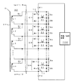
図1は、本発明による多直列蓄電セルの第1実施形態を示す。図同に示す多直列蓄電セルは多数(n)の蓄電セル11(B1〜Bn)を直列接続したものであって、その直列端P1,P2が電気自動車の動力となる電動機等の発電/負荷装置100に接続されて充放電使用されるようになっている。
FIG. 1 shows a first embodiment of a multi-series storage cell according to the present invention. The multi-series storage cell shown in the figure is a series connection of a large number (n) of storage cells 11 (B1 to Bn), and the series ends P1 and P2 of the power generation / load of an electric motor or the like that serves as power for the electric vehicle. It is connected to the
同図において、直列接続されたn個の蓄電セルB1〜Bnは、接続順で連続する2つのセル(B1とB2,B3とB4,・・・,Bn−1とBn)からなるセルグループ(G1,G2,G3,・・・,Gm)に分けられ、各セルグループ(G1,G2,G3,・・・,Gm)内にはそれぞれ、隣接セル間での電圧バランス補正を行うセル間電圧バランス補正回路31が設けられている。 In the figure, n power storage cells B1 to Bn connected in series are cell groups (B1 and B2, B3 and B4,..., Bn-1 and Bn) that are continuous in the connection order. G1, G2, G3,..., Gm), and each cell group (G1, G2, G3,..., Gm) has an intercell voltage for correcting the voltage balance between adjacent cells. A balance correction circuit 31 is provided.
セル間電圧バランス補正回路31は、インダクタLcとスイッチング回路Sa,Sbを用いて構成されるインダクタ結合方式の電圧バランス補正回路であって、隣接する第1のセル(B1,B3,・・・,Bn−1)と第2のセル(B2,B4,・・・,Bn)の間でインダクタ電流の充電と放電を行わせることにより、両セル間で電圧バランス補正を行う。 The inter-cell voltage balance correction circuit 31 is an inductor-coupled voltage balance correction circuit configured using the inductor Lc and the switching circuits Sa and Sb, and includes adjacent first cells (B1, B3,... By charging and discharging the inductor current between Bn-1) and the second cells (B2, B4,..., Bn), voltage balance correction is performed between the two cells.
スイッチング回路Sa,SbはMOS−FETを用いて構成され、図示を省略する制御回路から与えられる2相パルス信号により、交互にオン・オフ動作させられる。一方のスイッチング回路Saがオンのときは、第1のセル(B1,B3,・・・,Bn−1)からインダクタLcにインダクタ電流が充電される。このとき、他方のスイッチング回路Sbはオフされている。 The switching circuits Sa and Sb are configured using MOS-FETs and are alternately turned on and off by a two-phase pulse signal supplied from a control circuit (not shown). When one switching circuit Sa is on, the inductor current is charged from the first cell (B1, B3,..., Bn−1) to the inductor Lc. At this time, the other switching circuit Sb is turned off.
一方のスイッチング回路Saがオンからオフに切り換えられると、Lcに充電されたインダクタ電流は、他方のスイッチング回路Sbを通して第2のセル(B2,B4,・・・,Bn)を充電しながら放電されるようになる。 When one switching circuit Sa is switched from on to off, the inductor current charged to Lc is discharged through the other switching circuit Sb while charging the second cells (B2, B4,..., Bn). Become so.
ここで、セルB1とB2に着目し、B1の電圧がB2よりも高い場合は、B1によってインダクタLcに充電されたインダクタ電流がB2の充電経路で放電させられることにより、両セルB1,B2間の電圧が均等化される。反対に、B1の電圧がB2よりも低い場合は、B2によってインダクタLcに充電されたインダクタ電流がB1の充電経路で放電させられることにより、両セルB1,B2間の電圧が均等化される。 Here, paying attention to the cells B1 and B2, when the voltage of B1 is higher than B2, the inductor current charged to the inductor Lc by B1 is discharged through the charging path of B2, and thus between the cells B1 and B2. Are equalized. On the other hand, when the voltage of B1 is lower than B2, the inductor current charged in the inductor Lc by B2 is discharged through the charging path of B1, thereby equalizing the voltage between the cells B1 and B2.
つまり、隣接する2つのセルB1,B2間に電圧差があると、電圧が高い方のセルから低い方のセルに対して、インダクタンスLcを介して電気エネルギーの移転が行われることにより、両セルB1,B2の電圧が均等化される。このバランス補正動作は、各セルグループ(G1,G2,G3,・・・,Gm)内にてそれぞれ独立して行われる。 In other words, if there is a voltage difference between two adjacent cells B1 and B2, the electric energy is transferred from the cell having the higher voltage to the cell having the lower voltage via the inductance Lc. The voltages of B1 and B2 are equalized. This balance correction operation is performed independently in each cell group (G1, G2, G3,..., Gm).
各スイッチング回路Sa,Sbにはそれぞれダイオードが並列に接続されているが、このダイオードはMOS−FETのソース・ドレイン間に等価的に形成される寄生ダイオード(ボデーダイオード)によって形成されている。このダイオードはセル11の電圧に対しては逆方向となるが、インダクタ電流に対しては順方向となることにより、次のような効果をもたらす。
A diode is connected in parallel to each of the switching circuits Sa and Sb, and this diode is formed by a parasitic diode (body diode) formed equivalently between the source and drain of the MOS-FET. This diode is in the reverse direction with respect to the voltage of the
すなわち、スイッチング回路Sa,Sbが共にオフとなった期間にインダクタ電流が残留していた場合、その残留インダクタ電流はダイオードを通して流れ続けることができる。これにより、インダクタLcにいったん生じたインダクタ電流を電圧バランス補正動作に無駄なく利用できるとともに、そのインダクタ電流を遮断した場合に生じるサージ電圧の発生を確実に抑えることができる。 That is, if the inductor current remains during the period when both the switching circuits Sa and Sb are turned off, the remaining inductor current can continue to flow through the diode. As a result, the inductor current once generated in the inductor Lc can be used without waste for the voltage balance correction operation, and the generation of the surge voltage generated when the inductor current is cut off can be reliably suppressed.
図1に示す多直列蓄電セルには、上記セル間電圧バランス補正回路31に加えて、各セルグループ(G1,G2,G3,・・・,Gm)の直列電圧をバランス補正させるグループ間電圧バランス補正回路32が設置されている。
In the multi-series storage cell shown in FIG. 1, in addition to the inter-cell voltage balance correction circuit 31, an inter-group voltage balance for correcting the balance of the series voltage of each cell group (G1, G2, G3,..., Gm). A
このグループ間電圧バランス補正回路32は、トランスT1を用いたトランス結合方式の電圧バランス補正回路であって、同一磁心21に同一巻数で巻回されて相互に1対1の変圧比をなす複数のトランス・コイル(L1〜Lm)と、互いに同相でオン・オフ動作させられるスイッチング回路Scを用いて構成されている。
This inter-group voltage
各トランス・コイル(L1〜Lm)はそれぞれセルグループ(G1,G2,G3,・・・,Gm)の直列端に接続されている。スイッチング回路ScはMOS−FETを用いて構成され、図示を省略する制御回路から与えられる一定周期のパルス信号(クロック信号)により、互いに同相でオン・オフ動作する。 Each transformer coil (L1 to Lm) is connected to a series end of each cell group (G1, G2, G3,..., Gm). The switching circuit Sc is configured by using a MOS-FET, and is turned on / off in phase with each other in response to a pulse signal (clock signal) having a fixed period supplied from a control circuit (not shown).
このスイッチング回路Scにより、各セルグループ(G1,G2,G3,・・・,Gm)が互いに1対1の変圧比で交流結合される。これにより、各セルグループ(G1,G2,G3,・・・,Gm)の直列電圧が同電圧となるようなバランス補正が行われる。 By this switching circuit Sc, the cell groups (G1, G2, G3,..., Gm) are AC-coupled with each other at a transformation ratio of 1: 1. Thereby, balance correction is performed such that the series voltage of each cell group (G1, G2, G3,..., Gm) becomes the same voltage.
上述した多直列蓄電セルでは、セル(B1とB2,B3とB4,・・・,Bn−1とBn)をグループ化して、そのグループ(G1,G2,G3,・・・,Gm)内でそれぞれにインダクタ結合方式による隣接セルの電圧補正を行わせることにより、各セルグループ内での電圧バランス補正を迅速かつ円滑に行わせることができる。これと同時に、各セルグループ(G1,G2,G3,・・・,Gm)の直列電圧がトランス結合方式によってバランス補正されることにより、全セル(B1〜Bn)に対する電圧バランス補正を迅速かつ円滑に、しかも正確に行わせることができる。 In the multi-series storage cell described above, the cells (B1 and B2, B3 and B4,..., Bn-1 and Bn) are grouped, and within the group (G1, G2, G3,..., Gm). By causing each cell to perform voltage correction of adjacent cells by an inductor coupling method, voltage balance correction within each cell group can be performed quickly and smoothly. At the same time, the series voltage of each cell group (G1, G2, G3,..., Gm) is balance-corrected by the transformer coupling method, so that voltage balance correction for all cells (B1 to Bn) can be performed quickly and smoothly. In addition, it can be made to be accurate.
さらに、図1に示した実施形態では、インダクタ結合方式によるバランス補正を行わせるためのインダクタLcとスイッチング回路Sa,Sbが、2つのセル11に対して1組だけでよい。これにより、全セル(B1〜Bn)に対してインダクタ結合方式による電圧バランス補正を行う従来方式に比べて、インダクタLcおよびスイッチング回路Sa,Sbの部品数を大幅に低減させることができる。この部品数低減は、発熱量を低減させるとともに、セル(B1〜Bn)の実装密度(集合密度)を高める効果をもたらす。
Further, in the embodiment shown in FIG. 1, only one set of the inductor Lc and the switching circuits Sa and Sb for performing the balance correction by the inductor coupling method is required for the two
また、トランス結合方式による電圧バランス補正回路32は、トランス・コイル(L1〜Ln)とセルグループ(G1,G2,G3,・・・,Gm)間を接続する配線が必要になるが、この配線はセルグループ(G1,G2,G3,・・・,Gm)の数に1本を加えた(m+1)本でだけ良く、全セル(B1〜Bn)に対してトランス結合方式による電圧バランス補正を行う従来方式に比べると、配線数が大幅に低減されている。
In addition, the transformer-coupled voltage
上記により、直列接続数の多い多直列蓄電セルにおいて、組立てや交換等の作業性を向上させながら、全セルの電圧バランス補正を迅速かつ円滑に行わせることが可能である。 As described above, in a multi-series storage cell having a large number of series connections, it is possible to quickly and smoothly perform voltage balance correction for all the cells while improving workability such as assembly and replacement.
図2は、上記セルグループ(G1,G2,G3,・・・,Gm)の配線状態を実状態に近づけて示した回路図であるが、同図に示すように、各セルグループ(G1,G2,G3,・・・,Gm)ではそれぞれ2つのセルがモジュール化されている。多直列蓄電セルの組立てやセル交換等の作業は、そのモジュールを単位とすることにより効率的に行うことができる。 FIG. 2 is a circuit diagram showing the wiring state of the cell groups (G1, G2, G3,..., Gm) close to the actual state. As shown in FIG. In G2, G3,..., Gm), two cells are modularized. Operations such as assembly of multi-series storage cells and cell replacement can be efficiently performed by using the module as a unit.
図3は、インダクタ結合方式による電圧バランス補正回路31の実施形態を示す。この方式の電圧バランス補正回路31は、たとえば同図の(a)と(b)に示すような構成が可能である。 FIG. 3 shows an embodiment of a voltage balance correction circuit 31 using an inductor coupling method. The voltage balance correction circuit 31 of this system can be configured, for example, as shown in FIGS.
同図(a)に示す電圧バランス補正回路31は、図1または図2に示したセル間電圧バランス補正回路31と原理を同じくするものであって、隣接する第1のセルB1と第2のセルB2の間で、インダクタLcに対するインダクタ電流の充放電を行わせることにより、両セルB1,B2間で電圧バランス補正を行う。 The voltage balance correction circuit 31 shown in FIG. 6A is similar in principle to the inter-cell voltage balance correction circuit 31 shown in FIG. 1 or FIG. By charging and discharging the inductor current to and from the cell L2 between the cells B2, voltage balance correction is performed between the cells B1 and B2.
同図(b)に示す電圧バランス補正回路31は、第1のセルB1によって充電されたインダクタ電流を第2のセルB2の充電経路で放電する第1のインダクタLc1と、第2のセルB2によって充電されたインダクタ電流を第1のセルB1の充電経路で放電する第2のインダクタLc2と、上記第1および第2のインダクタLc1,Lc2の充電および放電の切換を行うスイッチング回路Sa,SbおよびダイオードD1,D2を用いて構成されている。 The voltage balance correction circuit 31 shown in FIG. 5B includes a first inductor Lc1 that discharges the inductor current charged by the first cell B1 through the charging path of the second cell B2, and a second cell B2. The second inductor Lc2 that discharges the charged inductor current through the charging path of the first cell B1, and the switching circuits Sa and Sb that switch the charging and discharging of the first and second inductors Lc1 and Lc2 and the diode D1 and D2 are used.
この回路31では、第1のスイッチング回路Saがオンのときに、第1のセルB1から第1のインダクタLc1にインダクタ電流が充電される。このインダクタ電流は、第1のスイッチング回路Saがオフになったときに、ダイオードD1を経由して第2のセルB2の充電経路で放電される。 In the circuit 31, when the first switching circuit Sa is on, the inductor current is charged from the first cell B1 to the first inductor Lc1. This inductor current is discharged through the charging path of the second cell B2 via the diode D1 when the first switching circuit Sa is turned off.
第1のスイッチング回路Saがオフのときは、第2のスイッチング回路Sbがオンになって、第2のセルB2から第2のインダクタLc2にインダクタ電流が充電される。このインダクタ電流は、第2のスイッチング回路Sbがオフになったときに、ダイオードD2を経由して第1のセルB1の充電経路で放電される。 When the first switching circuit Sa is off, the second switching circuit Sb is turned on, and the inductor current is charged from the second cell B2 to the second inductor Lc2. This inductor current is discharged through the charging path of the first cell B1 via the diode D2 when the second switching circuit Sb is turned off.
上記のように、同図(b)の電圧バランス補正回路31では、インダクタ電流の充電および放電によるバランス補正動作が、第1および第2セルB1,B2の双方で同時並行的に行われる。これにより、両セルB1,B2間での電圧バランス補正をさらに迅速化させることができる。 As described above, in the voltage balance correction circuit 31 in FIG. 5B, the balance correction operation by charging and discharging the inductor current is performed simultaneously in both the first and second cells B1 and B2. Thereby, the voltage balance correction between both cells B1 and B2 can be further accelerated.
図4は、トランス結合方式による電圧バランス補正回路32の実施形態を示す。この電圧バランス補正回路は、たとえば同図の(a)と(b)に示すような構成が可能である。
FIG. 4 shows an embodiment of a voltage
同図(a)に示す電圧バランス補正回路32は、図1または図2に示したグループ間電圧バランス補正回路32と原理を同じくするものであって、2つのセルグループG1、G2をそれぞれスイッチング回路Scを介してトランスT1のコイルL1,L2に接続することにより、2つのセルグループG1,G2を1対1の変圧比で交流結合させて電圧バランス補正を行う。
The voltage
各セルグループG1,G2はそれぞれ、k個の蓄電セル(B1〜Bk)が直列接続されてなるモジュールによって構成されている。各セルグループG1,G2内には、図示を省略するが、インダクタ結合方式によるセル間電圧バランス補正回路が設けられている。 Each of the cell groups G1 and G2 is configured by a module in which k power storage cells (B1 to Bk) are connected in series. In each cell group G1, G2, although not shown, an inter-cell voltage balance correction circuit using an inductor coupling method is provided.
同図(b)に示す電圧バランス補正回路32は、一次コイルLoと二次コイルL1,L2を有するトランスT1を使用する。一次コイルLoには、全セルグループ(G1,G2)の直列端(P1,P2)がスイッチング回路Scを介して接続されている。二次コイルL1,L2は各セルグループ(G1,G2)に整流および逆流防止用のダイオードD1,D2を介して接続される。
The voltage
二次コイルL1,L2は互いに同じ巻数で同一磁心21に巻回されている。一次コイルLoは、全セルの直列電圧でコア21を励磁できるよう、Scオン時にD1、D2がオフとなる方向の巻極にしてある。Scがオンになると全セルの直列電圧がLoに加わり、コア21を励磁する。次にScがオフになると、二次巻線L1、L2は、この励磁電流を維持するよう、D1、D2を通して電流を流す。このとき、巻数当りの電圧の低い方に電流は集中して流れることから、セルグループ(G1、G2)間で電圧バランス補正が行われる。
The secondary coils L1 and L2 are wound around the same
一次コイルLoには、全セルの直列電圧がスイッチング回路Scでオン・オフされながら印加される。この印加電圧は、所定の分圧比で変圧されて二次コイルL1,L2に現れる。二次コイルL1,L2に現れる分圧電圧は、ダイオードD1,D2を介してセルグループ(G1,G2)に印加される。これにより、セルグループ(G1,G2)間での電圧バランス補正が行われる。 A series voltage of all the cells is applied to the primary coil Lo while being turned on / off by the switching circuit Sc. This applied voltage is transformed at a predetermined voltage division ratio and appears in the secondary coils L1 and L2. The divided voltage appearing in the secondary coils L1, L2 is applied to the cell group (G1, G2) via the diodes D1, D2. Thereby, voltage balance correction between the cell groups (G1, G2) is performed.
このグループ間電圧バランス補正回路32は、全セルの直列電圧を各セルグループ(G1,G2)に一斉に再分配することによって電圧バランス補正を行うが、これにより、そのバランス補正動作を迅速化させることができる。
The inter-group voltage
図5は、本発明による多直列蓄電セルの第2実施形態を示す。図同に示す多直列蓄電セルは、各セルグループ(G1,G2,・・・)内にそれぞれ4つの蓄電セル11(B1〜B4,B5〜B8,・・・)が直列接続されている。つまり、4直列のセル(B1〜B4,B5〜B8,・・・)が単位となってセルグループ(G1,G2,・・・)のモジュールを構成している。 FIG. 5 shows a second embodiment of a multi-series storage cell according to the present invention. In the multi-series storage cell shown in the figure, four storage cells 11 (B1 to B4, B5 to B8,...) Are connected in series in each cell group (G1, G2,...). That is, four series cells (B1 to B4, B5 to B8,...) Constitute a cell group (G1, G2,...) Module.
各セルグループ(G1,G2,・・・)内には、インダクタ結合方式によるセル間電圧バランス補正回路31が設置されている。このセル間電圧バランス補正回路31は、2つのインダクタLc1,Lc2を用いている。両インダクタLc1,Lc2は同一磁心22に巻回されて互いに磁気結合している。すなわち、図6に示すように、インダクタLc1,Lc2は1対1のトランスを形成する。これにより、セル間電圧バランス補正回路31は、2つのインダクタLc1,Lc2で4つのセル(B1〜B4,・・・)の電圧をバランス補正させることができる。 In each cell group (G1, G2,...), An inter-cell voltage balance correction circuit 31 using an inductor coupling method is installed. The inter-cell voltage balance correction circuit 31 uses two inductors Lc1 and Lc2. Both inductors Lc1 and Lc2 are wound around the same magnetic core 22 and are magnetically coupled to each other. That is, as shown in FIG. 6, the inductors Lc1 and Lc2 form a one-to-one transformer. Thereby, the inter-cell voltage balance correction circuit 31 can perform the balance correction of the voltages of the four cells (B1 to B4,...) With the two inductors Lc1 and Lc2.
上記構成によれば、セルグループ(G1,G2,・・・)内の配線および部品数をさらに低減させることができる。また、各セルグループ(G1,G2,・・・)内の直列セル数が4個に増えたことにより、セルグループの数が大幅に低減されている。これにより、グループ間電圧バランス補正回路32のトランス・コイル数、およびグループ間電圧バランス補正回路32と蓄電セル列間の配線数をそれぞれ、さらに大幅に低減させることができる。
According to the above configuration, the number of wirings and parts in the cell group (G1, G2,...) Can be further reduced. Moreover, the number of series cells in each cell group (G1, G2,...) Has increased to four, so that the number of cell groups is greatly reduced. As a result, the number of transformers and coils of the inter-group voltage
以上、本発明をその代表的な実施形態に基づいて説明したが、本発明は上述した以外にも種々の態様が可能である。たとえば、セルグループ(G1,G2,・・・)内のセル数は3個あるいは5個以上の任意数が可能である。 As described above, the present invention has been described based on the representative embodiments, but the present invention can have various modes other than those described above. For example, the number of cells in the cell group (G1, G2,...) Can be 3 or an arbitrary number of 5 or more.
直列接続数の多い多直列蓄電セルにおいて、組立てや交換等の作業性を向上させながら、全セルの電圧バランス補正を迅速かつ円滑に行わせることを可能にした多直列蓄電セルを提供することができる。 To provide a multi-series storage cell capable of performing voltage balance correction of all cells quickly and smoothly while improving workability such as assembly and replacement in a multi-series storage cell having a large number of series connections. it can.
100 発電/負荷装置
11 蓄電セル11(B1〜Bn)
21,22 磁心
31 セル間電圧バランス補正回路
32 グループ間電圧バランス補正回路
G1〜Gm セルグループ
Lc,Lc1,Lc2 インダクタ
L1〜Lm トランス・コイル
P1,P2 多直列蓄電セル11の直列端
Sa,Sb,Sc スイッチング回路
T1 トランス
100 Power generation /
21, 22 Magnetic core 31 Voltage balance correction circuit between
Claims (6)
上記多直列蓄電セルを接続順で連続する複数の直列セルグループに分け、各直列セルグループ内にてそれぞれ隣接する蓄電セル間での電圧バランス補正を行うセル間電圧バランス補正回路を設け、セル間電圧バランス補正回路は、隣接する第1蓄電セルと第2蓄電セルに交互に接続されてインダクタ電流の充電および放電を行うインダクタを用いて構成されるとともに、
各直列セルグループを交流結合することによって各直列セルグループの直列電圧をバランス補正させるグループ間電圧バランス補正回路を設け、グループ間電圧バランス補正回路は、各直列セルグループの直列端にそれぞれ接続される複数のトランス・コイルと、一定周期のパルス信号により各トランス・コイルに同時に電流を流すスイッチング回路と、を用いて構成されることを特徴とする多直列蓄電セル。 A multi-series storage cell having a voltage balance correction circuit in which a plurality of storage cells are connected in series and equalize the voltage of each storage cell,
The multi-series storage cells are divided into a plurality of series cell groups that are continuous in the connection order, and an inter-cell voltage balance correction circuit that performs voltage balance correction between adjacent storage cells in each series cell group is provided . voltage balance correction circuit is configured by using an inductor for charging and discharging of the first battery cell and connected to the inductor current alternately to the second storage cell adjacent Rutotomoni,
The inter-group voltage balance correction circuit to balance correcting the series voltage of each of the series cell groups provided by the AC coupling each series cell groups, the voltage balance correction circuit between the groups are connected in series ends of each of the series cell groups multi-series storage cells, characterized in that constructed by using a plurality of transformer coils, and a switching circuit for supplying at the same time current to each transformer coil by a pulse signal having a constant period.
Priority Applications (3)
| Application Number | Priority Date | Filing Date | Title |
|---|---|---|---|
| JP2006208992A JP5039335B2 (en) | 2006-07-31 | 2006-07-31 | Multi-series storage cell |
| PCT/JP2007/062478 WO2007148745A1 (en) | 2006-06-22 | 2007-06-21 | Multi-series accumulation cell, series accumulation cell device, and series cell voltage balance correction circuit |
| US12/305,518 US8692515B2 (en) | 2006-06-22 | 2007-06-21 | Series-connected rechargeable cells, series-connected rechargeable cell device, voltage-balance correcting circuit for series-connected cells |
Applications Claiming Priority (1)
| Application Number | Priority Date | Filing Date | Title |
|---|---|---|---|
| JP2006208992A JP5039335B2 (en) | 2006-07-31 | 2006-07-31 | Multi-series storage cell |
Publications (2)
| Publication Number | Publication Date |
|---|---|
| JP2008035680A JP2008035680A (en) | 2008-02-14 |
| JP5039335B2 true JP5039335B2 (en) | 2012-10-03 |
Family
ID=39124500
Family Applications (1)
| Application Number | Title | Priority Date | Filing Date |
|---|---|---|---|
| JP2006208992A Active JP5039335B2 (en) | 2006-06-22 | 2006-07-31 | Multi-series storage cell |
Country Status (1)
| Country | Link |
|---|---|
| JP (1) | JP5039335B2 (en) |
Families Citing this family (13)
| Publication number | Priority date | Publication date | Assignee | Title |
|---|---|---|---|---|
| JP5200571B2 (en) | 2008-02-18 | 2013-06-05 | 富士通セミコンダクター株式会社 | Semiconductor device and photomask manufacturing method |
| TWI385895B (en) * | 2009-04-30 | 2013-02-11 | Cheng Uei Prec Ind Co Ltd | Battery charging circuit |
| EP2587614A2 (en) | 2011-08-31 | 2013-05-01 | Sony Corporation | Electric storage apparatus, electronic device, electric vehicle, and electric power system |
| JP5760877B2 (en) * | 2011-09-07 | 2015-08-12 | 日産自動車株式会社 | Battery control device |
| JP5821619B2 (en) | 2011-12-26 | 2015-11-24 | ソニー株式会社 | Power storage device, power system, and electric vehicle |
| JP2013247690A (en) * | 2012-05-23 | 2013-12-09 | Toyota Industries Corp | Voltage equalization device |
| WO2013187316A1 (en) * | 2012-06-13 | 2013-12-19 | 株式会社豊田自動織機 | Voltage equalization device and method |
| EP2760115A1 (en) * | 2013-01-24 | 2014-07-30 | Siemens Aktiengesellschaft | Method for balancing of capacitor voltages in a link circuit |
| JP6428107B2 (en) | 2014-09-29 | 2018-11-28 | 株式会社村田製作所 | Power storage device, electronic device, electric vehicle and power system |
| JP6509005B2 (en) | 2015-03-30 | 2019-05-08 | Fdk株式会社 | Voltage balance correction circuit |
| JP6928347B2 (en) * | 2017-08-02 | 2021-09-01 | NExT−e Solutions株式会社 | Management device, power storage device, power storage system, and electrical equipment |
| JP7344435B2 (en) * | 2019-06-03 | 2023-09-14 | マツダ株式会社 | vehicle drive system |
| JP7254270B2 (en) * | 2019-06-03 | 2023-04-10 | マツダ株式会社 | vehicle drive |
Family Cites Families (3)
| Publication number | Priority date | Publication date | Assignee | Title |
|---|---|---|---|---|
| DE4422409C2 (en) * | 1994-06-29 | 1996-07-11 | Fraunhofer Ges Forschung | Device for the exchange of charges between a plurality of energy stores or converters connected in series |
| JPH10257683A (en) * | 1997-03-07 | 1998-09-25 | Japan Storage Battery Co Ltd | Charging-discharging circuit for combined batteries |
| JP3764633B2 (en) * | 2000-06-26 | 2006-04-12 | Necトーキン株式会社 | Electric energy storage device, cell energy amount adjusting device, and cell energy amount adjusting method |
-
2006
- 2006-07-31 JP JP2006208992A patent/JP5039335B2/en active Active
Also Published As
| Publication number | Publication date |
|---|---|
| JP2008035680A (en) | 2008-02-14 |
Similar Documents
| Publication | Publication Date | Title |
|---|---|---|
| JP5039335B2 (en) | Multi-series storage cell | |
| WO2007148745A1 (en) | Multi-series accumulation cell, series accumulation cell device, and series cell voltage balance correction circuit | |
| US7151364B2 (en) | DC/DC converter and program | |
| WO2013061461A1 (en) | Battery system | |
| JP2009540793A (en) | Charge equalization device in which secondary windings of multiple transformers are connected in parallel | |
| JP2013110778A (en) | Power supply device and method of controlling power supply device | |
| EP1910124A1 (en) | Multilevel converter and method of converting a supply voltage | |
| JP6489099B2 (en) | Power supply circuit including converter and power supply system using the same | |
| CN103296712A (en) | Charging circuits for energy storage device and method for charging energy storage device | |
| JP2020039228A (en) | Voltage conversion device | |
| JP2017103880A (en) | Power conversion device | |
| US10978953B2 (en) | Flyback power supply, inverter and electrically powered vehicle | |
| CN103296714B (en) | Charging circuits for energy storage apparatus and method for charging for energy storage apparatus | |
| JP2010104077A (en) | Battery balancing circuit | |
| CN100373757C (en) | Power supply apparatus | |
| KR20230004736A (en) | Automotive Battery Chargers, Related Vehicles, and Implementation Methods | |
| CN103296910B (en) | Direct voltage capture device for energy storage device and method for generating direct voltage by energy storage device | |
| CN110896236B (en) | Power supply device | |
| JP6994428B2 (en) | Storage battery charging device | |
| JP6953634B2 (en) | Vehicle charger with DC / DC converter | |
| JP6146321B2 (en) | Power supply | |
| US11095128B2 (en) | Voltage balance correction circuit | |
| KR102595965B1 (en) | Multilevel converter | |
| US8107265B2 (en) | Current balanced push-pull inverter circuit with regeneration snubber circuit and voltage boost section | |
| CN117894562A (en) | Transformer for DC voltage conversion and for electrical systems for charging vehicle batteries |
Legal Events
| Date | Code | Title | Description |
|---|---|---|---|
| A621 | Written request for application examination |
Free format text: JAPANESE INTERMEDIATE CODE: A621 Effective date: 20081028 |
|
| A131 | Notification of reasons for refusal |
Free format text: JAPANESE INTERMEDIATE CODE: A131 Effective date: 20110906 |
|
| A521 | Request for written amendment filed |
Free format text: JAPANESE INTERMEDIATE CODE: A523 Effective date: 20111104 |
|
| TRDD | Decision of grant or rejection written | ||
| A01 | Written decision to grant a patent or to grant a registration (utility model) |
Free format text: JAPANESE INTERMEDIATE CODE: A01 Effective date: 20120612 |
|
| A01 | Written decision to grant a patent or to grant a registration (utility model) |
Free format text: JAPANESE INTERMEDIATE CODE: A01 |
|
| A61 | First payment of annual fees (during grant procedure) |
Free format text: JAPANESE INTERMEDIATE CODE: A61 Effective date: 20120709 |
|
| FPAY | Renewal fee payment (event date is renewal date of database) |
Free format text: PAYMENT UNTIL: 20150713 Year of fee payment: 3 |
|
| R150 | Certificate of patent or registration of utility model |
Ref document number: 5039335 Country of ref document: JP Free format text: JAPANESE INTERMEDIATE CODE: R150 Free format text: JAPANESE INTERMEDIATE CODE: R150 |
|
| S531 | Written request for registration of change of domicile |
Free format text: JAPANESE INTERMEDIATE CODE: R313531 |
|
| R350 | Written notification of registration of transfer |
Free format text: JAPANESE INTERMEDIATE CODE: R350 |
|
| R250 | Receipt of annual fees |
Free format text: JAPANESE INTERMEDIATE CODE: R250 |
|
| R250 | Receipt of annual fees |
Free format text: JAPANESE INTERMEDIATE CODE: R250 |
|
| R250 | Receipt of annual fees |
Free format text: JAPANESE INTERMEDIATE CODE: R250 |
|
| R250 | Receipt of annual fees |
Free format text: JAPANESE INTERMEDIATE CODE: R250 |
|
| R250 | Receipt of annual fees |
Free format text: JAPANESE INTERMEDIATE CODE: R250 |
|
| R250 | Receipt of annual fees |
Free format text: JAPANESE INTERMEDIATE CODE: R250 |
|
| R250 | Receipt of annual fees |
Free format text: JAPANESE INTERMEDIATE CODE: R250 |
|
| R250 | Receipt of annual fees |
Free format text: JAPANESE INTERMEDIATE CODE: R250 |
|
| R250 | Receipt of annual fees |
Free format text: JAPANESE INTERMEDIATE CODE: R250 |
|
| R250 | Receipt of annual fees |
Free format text: JAPANESE INTERMEDIATE CODE: R250 |