JP4922979B2 - Semiconductor substrate - Google Patents
Semiconductor substrate Download PDFInfo
- Publication number
- JP4922979B2 JP4922979B2 JP2008087396A JP2008087396A JP4922979B2 JP 4922979 B2 JP4922979 B2 JP 4922979B2 JP 2008087396 A JP2008087396 A JP 2008087396A JP 2008087396 A JP2008087396 A JP 2008087396A JP 4922979 B2 JP4922979 B2 JP 4922979B2
- Authority
- JP
- Japan
- Prior art keywords
- layer
- substrate
- lattice constant
- semiconductor layer
- semiconductor
- Prior art date
- Legal status (The legal status is an assumption and is not a legal conclusion. Google has not performed a legal analysis and makes no representation as to the accuracy of the status listed.)
- Expired - Fee Related
Links
- 239000004065 semiconductor Substances 0.000 title claims description 95
- 239000000758 substrate Substances 0.000 title claims description 89
- 229910001218 Gallium arsenide Inorganic materials 0.000 claims description 19
- 239000010410 layer Substances 0.000 description 171
- 239000010409 thin film Substances 0.000 description 25
- 238000000034 method Methods 0.000 description 15
- 239000010408 film Substances 0.000 description 14
- 230000007547 defect Effects 0.000 description 13
- 229910000530 Gallium indium arsenide Inorganic materials 0.000 description 10
- 238000010586 diagram Methods 0.000 description 10
- 230000003287 optical effect Effects 0.000 description 8
- 230000008859 change Effects 0.000 description 6
- 150000001875 compounds Chemical class 0.000 description 6
- 239000013078 crystal Substances 0.000 description 6
- 239000000463 material Substances 0.000 description 6
- 238000001451 molecular beam epitaxy Methods 0.000 description 6
- 230000001678 irradiating effect Effects 0.000 description 4
- 238000004519 manufacturing process Methods 0.000 description 4
- 229910000980 Aluminium gallium arsenide Inorganic materials 0.000 description 3
- 230000015572 biosynthetic process Effects 0.000 description 3
- 229910000673 Indium arsenide Inorganic materials 0.000 description 2
- 238000004891 communication Methods 0.000 description 2
- 238000007796 conventional method Methods 0.000 description 2
- 230000000694 effects Effects 0.000 description 2
- RPQDHPTXJYYUPQ-UHFFFAOYSA-N indium arsenide Chemical compound [In]#[As] RPQDHPTXJYYUPQ-UHFFFAOYSA-N 0.000 description 2
- 230000002040 relaxant effect Effects 0.000 description 2
- 239000002356 single layer Substances 0.000 description 2
- 230000007704 transition Effects 0.000 description 2
- QVGXLLKOCUKJST-UHFFFAOYSA-N atomic oxygen Chemical compound [O] QVGXLLKOCUKJST-UHFFFAOYSA-N 0.000 description 1
- 238000005229 chemical vapour deposition Methods 0.000 description 1
- 230000007423 decrease Effects 0.000 description 1
- 238000005516 engineering process Methods 0.000 description 1
- 230000002349 favourable effect Effects 0.000 description 1
- 230000005669 field effect Effects 0.000 description 1
- 230000004907 flux Effects 0.000 description 1
- WPYVAWXEWQSOGY-UHFFFAOYSA-N indium antimonide Chemical compound [Sb]#[In] WPYVAWXEWQSOGY-UHFFFAOYSA-N 0.000 description 1
- 238000009413 insulation Methods 0.000 description 1
- 230000007246 mechanism Effects 0.000 description 1
- 239000002184 metal Substances 0.000 description 1
- 229910052751 metal Inorganic materials 0.000 description 1
- 238000002488 metal-organic chemical vapour deposition Methods 0.000 description 1
- 229910052760 oxygen Inorganic materials 0.000 description 1
- 239000001301 oxygen Substances 0.000 description 1
- 230000003071 parasitic effect Effects 0.000 description 1
Images


Landscapes
- Physical Vapour Deposition (AREA)
- Junction Field-Effect Transistors (AREA)
- Physical Deposition Of Substances That Are Components Of Semiconductor Devices (AREA)
- Recrystallisation Techniques (AREA)
- Crystals, And After-Treatments Of Crystals (AREA)
Description
本発明は、半導体基板に関し、より詳細には、基板と格子定数の異なる半導体層が基板上に形成された半導体基板に関する。 The present invention relates to a semiconductor substrate, and more particularly to a semiconductor substrate in which a semiconductor layer having a lattice constant different from that of a substrate is formed on the substrate.
GaAsをはじめとするIII−V族の化合物半導体は、高い電子移動度を有すること、また、発光デバイスに適した直接遷移型半導体であることなどから、光デバイスや高速トランジスタに広く用いられてきた。 III-V compound semiconductors such as GaAs have been widely used in optical devices and high-speed transistors because they have high electron mobility and are direct transition semiconductors suitable for light-emitting devices. .
光デバイスの分野では、半導体のバンドギャップが発光、もしくは受光波長を決めるため、波長に応じて各種の材料が用いられるが、これらを形成する基板としては、大口径の基板が工業的に安定に得られることから、主としてGaAsが用いられてきた。また、GaAsよりは大口径化しにくく高価ではあるが、必要とする半導体層の材料に応じて、InP、あるいはGaP基板が用いられることもあった。 In the field of optical devices, the band gap of a semiconductor determines the wavelength of light emitted or received, so various materials are used depending on the wavelength. As a substrate for forming these, a large-diameter substrate is industrially stable. Since it is obtained, GaAs has been mainly used. Further, although it is harder to increase the diameter than GaAs and is expensive, an InP or GaP substrate may be used depending on the required semiconductor layer material.
一方、高速トランジスタの分野では、通信データ量の増大に起因する通信周波数の高周波化や広帯域化の要求に応えるために、Siに比べ、10倍以上の電子移動度を有するGaAsの電界効果型トランジスタ(MESFET)や、GaAsとAlGaAsのヘテロ構造を用いた高電子移動度トランジスタ(HEMT、もしくはHFET)などが実用化されてきた。さらには電子走行層であるGaAsをより高い電子移動度を有するInGaAsに置き換えたHEMTも提案されてきた。 On the other hand, in the field of high-speed transistors, a GaAs field effect transistor having an electron mobility of 10 times or more compared with Si in order to meet the demand for higher communication frequency and wider bandwidth due to an increase in communication data volume. (MESFET) and high electron mobility transistors (HEMT or HFET) using a heterostructure of GaAs and AlGaAs have been put into practical use. Furthermore, a HEMT in which GaAs, which is an electron transit layer, is replaced with InGaAs having higher electron mobility has been proposed.
これらのトランジスタは、同じIII−V族であり、電気的にも絶縁性のある基板が得られるうえ、工業的に安定に、かつ低価格で大口径の基板が得られるという理由から、主としてGaAs基板を用いて製造されてきた。 These transistors are of the same III-V group, and an electrically insulating substrate can be obtained, and a large-diameter substrate can be obtained industrially stably and at a low price. It has been manufactured using a substrate.
しかしながら、こうしたトランジスタにおける電子走行層(以下、チャネル層という)、もしくは光デバイスにおける活性層と、基板の格子定数の関係には制約があった。高速トランジスタを例にとると、電子移動度の高いチャネル層を基板上に形成する際、分子線エピタキシー法(以下、MBE法という)、もしくは有機金属気相成長法(以下、MOCVD法という)などを用いたエピタキシャル成長により形成するが、基板とチャネル層、もしくは活性層との間に格子不整合があると、薄膜成長中に応力により多結晶、もしくはアモルファス状態の薄膜となり膜質が極端に劣化する。 However, the relationship between the electron constant layer (hereinafter referred to as channel layer) in such a transistor or the active layer in an optical device and the lattice constant of the substrate is limited. Taking a high-speed transistor as an example, when a channel layer having high electron mobility is formed on a substrate, a molecular beam epitaxy method (hereinafter referred to as MBE method), a metal organic chemical vapor deposition method (hereinafter referred to as MOCVD method), or the like. However, if there is a lattice mismatch between the substrate and the channel layer or the active layer, a thin film in a polycrystalline or amorphous state is formed by stress during the thin film growth, and the film quality is extremely deteriorated.
こうした問題を避けるため、これまでに主に製品化されてきたのは、基板の格子定数に実質的に格子整合する格子整合系であった。具体的には、高速トランジスタの場合、GaAsと格子整合するAlGaAsとGaAsをGaAs基板上に形成する系、もしくは格子定数に若干差があっても単結晶の薄膜が成長できる膜厚、いわゆる臨界膜厚の範囲で薄膜を形成する擬似格子整合系トランジスタとして、AlGaAsとInGaAsを用いるものである。 In order to avoid such problems, what has been mainly commercialized so far is a lattice matching system that substantially matches the lattice constant of the substrate. Specifically, in the case of a high-speed transistor, a system in which AlGaAs and GaAs lattice-matched with GaAs are formed on a GaAs substrate, or a film thickness capable of growing a single-crystal thin film even if there is a slight difference in lattice constant, a so-called critical film AlGaAs and InGaAs are used as pseudo-lattice matching transistors that form a thin film within a thickness range.
擬似格子整合系トランジスタでは、InGaAsのIn組成比を高くするほど電子移動度は高くなり、高周波動作には適するものの、基板との格子定数差は大きくなり、トランジスタの動作に最低限必要な膜厚をエピタキシャル成長させることができなるため、Inの組成は最大でも20%が限界であった。従って、高速トランジスタでは、より高速動作を実現するためにはゲート長の微細化を行うしかなく、光デバイスにおいては使用できる波長に限界があった。 In a pseudo-lattice matching transistor, the higher the In composition ratio of InGaAs, the higher the electron mobility, which is suitable for high-frequency operation. However, the difference in lattice constant from the substrate increases, and the minimum film thickness required for transistor operation. Therefore, the maximum composition of In is 20%. Therefore, in a high-speed transistor, in order to realize a higher-speed operation, the gate length must be reduced, and there is a limit to the wavelength that can be used in an optical device.
こうした問題を解決するために、基板から電子走行層、あるいは活性層に至る薄膜部分で2層間の格子不整合を緩和するための格子不整合緩和層(以下、バッファ層という)を本来基板上に形成したい薄膜と基板の間に設けることで、基板の格子定数に関係なく、任意の格子定数のチャネル層、もしくは活性層を形成するための各種の手法が検討されてきた。 In order to solve these problems, a lattice mismatch relaxation layer (hereinafter referred to as a buffer layer) for relaxing lattice mismatch between two layers in the thin film portion from the substrate to the electron transit layer or the active layer is originally provided on the substrate. Various methods for forming a channel layer or an active layer having an arbitrary lattice constant regardless of the lattice constant of the substrate have been studied by providing it between the thin film to be formed and the substrate.
まず、非特許文献1に開示されているように、基板の格子定数から連続的、あるいは段階的に薄膜の組成を変化させることで、格子不整合を緩和するグレーデッドバッファ層と呼ばれる手法がある。この方法は、実際の膜構造としては各種の構造があるが、共通しているのは半導体の組成を連続的、あるいは段階的に変化させることで、格子定数を変化させ、本来能動層として使用したい層(この場合は、InAlAs/InGaAs層)の格子定数に揃ったところで、グレーデッド構造を停止し、均一な層(この場合は、InAlAs層)を形成していくというものである。
First, as disclosed in Non-Patent
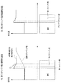
そこで、以下にグレーデッドバッファ層の方式と特徴について説明する。
図1(a),(b)は、グレーデッドバッファ層の概念図で、図1(a)は、連続的なグレーデッドバッファ層の場合を示し、図1(b)は、段階的なグレーデッドバッファ層の場合を示している。
Therefore, the method and characteristics of the graded buffer layer will be described below.
1A and 1B are conceptual diagrams of a graded buffer layer. FIG. 1A shows the case of a continuous graded buffer layer, and FIG. The case of the dead buffer layer is shown.
つまり、図1(a)は、基板側から連続的に半導体組成を変化させることで、基板の格子定数から、トランジスタであれば電子走行層として使用したい半導体層の格子定数まで連続的に変化させるものである。実際にMBE法によりこの構造を成膜する場合、変化させたい材料のセル温度、及び基板温度を変化させながら成膜を行うため、製造時の制御がしにくい場合があった。そこで、図1(b)に示すように、段階的に格子定数を変化させる段階的にステップグレーデッドバッファの方法も提案されてきた。 That is, in FIG. 1A, by continuously changing the semiconductor composition from the substrate side, the lattice constant of the substrate is continuously changed from the lattice constant of the semiconductor layer to be used as an electron transit layer in the case of a transistor. Is. When this structure is actually formed by the MBE method, since the film formation is performed while changing the cell temperature and the substrate temperature of the material to be changed, it may be difficult to control during manufacturing. Therefore, as shown in FIG. 1B, a step-graded buffer method has been proposed in which the lattice constant is changed step by step.
これらのグレーデッドバッファ構造の特徴は、格子定数差を緩和するために発生する転移、あるいは欠陥が、基板の面に対して平行に、あるいは層状に発生することである。 A characteristic of these graded buffer structures is that transitions or defects that occur in order to relieve the lattice constant difference occur in parallel or in layers with respect to the surface of the substrate.
図2は、グレーデッドバッファ層における結晶欠陥の発生を示す模式図で、図中符号21は基板、22はグレーデッドバッファ層、23はチャネル層(活性層)を示している。この構造では、グレーデッドバッファ層22の上部に形成されるトランジスタや光デバイスのチャネル層、もしくは活性層23など、格子欠陥aがデバイスの特性に直接影響する層まで欠陥が伸びにくいため、デバイスの特性の点では好ましい構造となる。一方で、基板21との格子定数差が大きくなると、それに応じてグレーデッドバッファ層22の厚さを厚くしなければならなかった。 FIG. 2 is a schematic diagram showing the occurrence of crystal defects in the graded buffer layer. In the figure, reference numeral 21 denotes a substrate, 22 denotes a graded buffer layer, and 23 denotes a channel layer (active layer). In this structure, since the defects are difficult to extend to a layer in which the lattice defect a directly affects the device characteristics, such as a transistor formed on the graded buffer layer 22, a channel layer of the optical device, or the active layer 23, The structure is preferable in terms of characteristics. On the other hand, when the lattice constant difference with the substrate 21 increases, the thickness of the graded buffer layer 22 must be increased accordingly.
何故なら、格子定数を変化させるためには、薄膜の組成を変化させる必要があるが、組成を急激に変化させるとグレーデッドバッファ層本来の特徴である格子不整合の緩和機構がうまく働かない。しかも、組成を急激に変化させるには、MBE法であればフラックスの強度をセル温度の変化により制御するしかないため、セルの熱容量で決まる時定数以上には、変化させることはできない。このため、薄膜成長に必要な時間が長くなり、製造コストが高くなるという欠点があった。 This is because in order to change the lattice constant, it is necessary to change the composition of the thin film. However, if the composition is changed rapidly, the relaxation mechanism of the lattice mismatch, which is a characteristic feature of the graded buffer layer, does not work well. Moreover, in order to change the composition abruptly, the intensity of the flux can only be controlled by changing the cell temperature in the case of the MBE method, so it cannot be changed beyond the time constant determined by the heat capacity of the cell. For this reason, the time required for the thin film growth becomes longer, and there is a disadvantage that the manufacturing cost is increased.
これとは対照的に、例えば、特許文献1に示すように、基板上に直に格子定数の異なる薄膜層を形成し、この薄膜層で格子緩和を行う方法もある。この特許文献1に記載のものは、衛星放送の送受信用増幅素子や高速データ転送用素子として、優れた高周波特性を有するFETを提供することを目的としたもので、InAsと異なる格子定数を有する半導体基板上に、バッファ層として機能する第1の化合物半導体層と、電子走行層として機能するInAs層とを順次積層した構成を有しているものである。
In contrast, for example, as shown in
この場合は、薄膜層中で組成の変化をさせたりしないため、構造は簡単であり、成膜条件の管理は容易になり好ましいが、格子定数差による欠陥の発生が基板に対して上方まで伸びやすく、バッファ層の厚さを厚くしても欠陥密度が下がりにくいという欠点があった。 In this case, since the composition is not changed in the thin film layer, the structure is simple and the film formation conditions can be easily managed. However, the generation of defects due to the difference in lattice constant extends upward with respect to the substrate. There is a drawback that the defect density is not easily lowered even if the buffer layer is made thick.
図3は、単層バッファにおける結晶欠陥の発生を示す模式図で、図中符号31は基板、32はバッファ層、33はチャネル層(活性層)を示している。特にトランジスタや光デバイスなど、格子欠陥aに対して敏感なデバイスでは、バッファ層32を厚くしても結晶欠陥に起因する特性の劣化があるため、問題となっていた。 FIG. 3 is a schematic diagram showing the occurrence of crystal defects in a single-layer buffer, in which reference numeral 31 denotes a substrate, 32 denotes a buffer layer, and 33 denotes a channel layer (active layer). In particular, a device sensitive to the lattice defect a, such as a transistor or an optical device, has a problem because even if the buffer layer 32 is made thick, characteristics are deteriorated due to crystal defects.
本発明は、このような問題に鑑みてなされたもので、その目的とするところは、従来に比べ極めて薄いバッファ層を用いて、工業的に安定に、かつ低コストで、基板と格子定数の異なる良質の薄膜を形成した半導体基板を提供することにある。 The present invention has been made in view of such problems. The object of the present invention is to use an extremely thin buffer layer as compared with the prior art, which is industrially stable and low in cost, and has a substrate and a lattice constant. The object is to provide a semiconductor substrate on which different quality thin films are formed.
本発明者は、AlGaAsSbや、InAlSb等、Sbを含有する化合物半導体層が、極めて薄い層で格子定数を緩和する特長を利用し、その上層に格子定数の大きい側から小さい側にグレーデッドバッファ層を形成したとき、従来に比べ薄いバッファ層で格子欠陥の少ない良質の薄膜が形成できることを見出して本発明をなすに至った。 The present inventor utilizes the feature that the compound semiconductor layer containing Sb, such as AlGaAsSb and InAlSb, relaxes the lattice constant with a very thin layer, and the graded buffer layer is formed on the upper layer from the side having the larger lattice constant to the side having the smaller lattice constant. As a result, it was found that a high-quality thin film with fewer lattice defects can be formed with a thinner buffer layer than in the prior art, and the present invention has been made.
本発明は、このような目的を達成するためになされたもので、請求項1に記載の発明は、格子定数xを有する基板と、該基板上に形成され、格子定数yを有し、少なくともSbを含む第1の半導体層と、該第1の半導体層上に形成され、格子定数yからzまで格子定数を段階的又は連続的に変化させた第2の半導体層と、該第2の半導体層上に形成され、格子定数zを有する第3の半導体層を有し、前記格子定数の関係が、x<z<yの関係にあることを特徴とする。
The present invention has been made to achieve such an object. The invention according to
また、請求項2に記載の発明は、請求項1に記載の発明において、前記第1の半導体層が、AlGaAsSbであることを特徴とする。
The invention according to
また、請求項3に記載の発明は、請求項1に記載の発明において、前記第1の半導体層が、InAlGaAsSbであることを特徴とする。
The invention according to
また、請求項4に記載の発明は、請求項1に記載の発明において、前記基板が、GaAsであることを特徴とする。 According to a fourth aspect of the present invention, in the first aspect of the present invention, the substrate is GaAs.
また、請求項5に記載の発明は、請求項1に記載の発明において、前記基板が、InPであることを特徴とする。 According to a fifth aspect of the present invention, in the first aspect of the present invention, the substrate is InP.
また、請求項6に記載の発明は、請求項1に記載の発明において、前記第3の半導体層が、InAlAsであることを特徴とする。 According to a sixth aspect of the invention, in the first aspect of the invention, the third semiconductor layer is InAlAs.
また、請求項7に記載の発明は、請求項6に記載の発明において、前記第3の半導体層が、InxAl1-xAsであって、0.2<x<0.8であることを特徴とする。 The invention according to claim 7 is the invention according to claim 6, wherein the third semiconductor layer is In x Al 1-x As, and 0.2 <x <0.8. It is characterized by that.
また、請求項8に記載の発明は、請求項1に記載の発明において、前記第3の半導体層が、InAlGaAsSbであることを特徴とする。
The invention according to claim 8 is the invention according to
本発明の薄膜構造を用いると、基板の格子定数に対して、格子定数の大きな半導体薄膜を従来の方法より大幅に薄いバッファ層で良質の薄膜を形成することができる。このため、薄膜成長に要する時間が短縮できるだけでなく、良質の薄膜が安定して製造できるという効果を奏する。 When the thin film structure of the present invention is used, a high-quality thin film can be formed from a semiconductor thin film having a large lattice constant relative to the lattice constant of the substrate by using a buffer layer that is significantly thinner than the conventional method. For this reason, not only the time required for thin film growth can be shortened, but also an effect that a high quality thin film can be produced stably is produced.
以下、図面を参照して本発明の実施の形態について説明する。
図4は、本発明の半導体基板の基本構造を示す断面構成図で、図中符号1は基板、2は第1の半導体層、3は第2の半導体層、4は第3の半導体層を示している。
Embodiments of the present invention will be described below with reference to the drawings.
FIG. 4 is a cross-sectional view showing the basic structure of the semiconductor substrate of the present invention. In the figure,
本発明の半導体基板は、基板1と、第1の半導体層2と、第2の半導体層3と、第3の半導体層4とからなり、基板1は、格子定数xを有するものである。第1の半導体層2は、基板1上に形成され、格子定数yを有し、少なくともSbを含んでいる。第2の半導体層3は、第1の半導体層2上に形成され、格子定数yからzまで格子定数を段階的又は連続的に変化させものである。第3の半導体層4は、第2の半導体層3上に形成され、格子定数zを有するものある。そして、これらの格子定数の関係は、x<z<yの関係を有している。
The semiconductor substrate of the present invention includes a
基板1は、GaAs又はInPであることが好ましいが、化合物半導体の成長に適したものであれば何でも良い。安価に大口径の基板が得られるという点で、GaAs基板が最も好ましい。この他、基板上に形成する半導体層に応じて、InP基板やGaP基板なども用いられる。トランジスタの場合、高周波信号の損失、寄生容量等を低減するために基板の絶縁性が高いことが要求されるため、107Ω・cm程度以上の半絶縁性基板が最もよく用いられる。一方、基板の導電性が必要な発光デバイスなどの場合には、n型、もしくはp型にドープされた基板を用いることもあり、必要に応じて適宜使い分けることができる。
The
次に、第1の半導体層2は、AlGaAsSb又はInAlGaAsSbであることが好ましいが、格子不整合を緩和するバッファ層としての機能を有する層であり、少なくともSbを含有する化合物半導体層からなる。Sbを含む半導体層は、他の材料系と比べ格子緩和が早く、成長を開始してから数原子層で、エピタキシャル成長を開始し、50nm程度の薄膜で材料の組成に応じた格子定数の薄膜が形成されるようになる。従って、第1の半導体層の厚さは、最低1原子層以上必要であり、上限は特にないが、成膜に必要な時間がかかることや、ある厚さ以上形成してもバッファ層としての機能は変わらないことから、最大1umの厚さがあれば十分である。ここに用いられる材料は、必要とするデバイスの種類により、絶縁性が必要な場合と、導電性のほうが好ましい場合とあるが、絶縁性のバッファ層として用いられるものは、AlGaAsSb、もしくはInAlGaAsSbなどが好ましい。
Next, the
また、HBT(ヘテロ接合バイポーラトランジスタ)や、光デバイス系のように第1の半導体層が導電性のほうが好ましい場合は、InSbが極めて格子緩和性に優れており、しかも抵抗も低くできることから適している。これは、最終的に形成したい薄膜層が、一般的にはInGaAs系、もしくはInAsSb系であり、極力共通した元素を含有するものが好ましいためである。 In addition, when the first semiconductor layer is more conductive, such as an HBT (heterojunction bipolar transistor) or an optical device system, InSb is extremely excellent in lattice relaxation and can be reduced in resistance. Yes. This is because the thin film layer to be finally formed is generally InGaAs-based or InAsSb-based, and preferably contains a common element as much as possible.
チャネル層、あるいは活性層としてInGaAs層を用いる場合は、成膜時の制御性、絶縁性の点でAlGaAsSbが最も好ましい。また同様に、InAsSb系を使う場合は、AlGaAsSb系よりも格子定数が大きく取れるInAlAsSb系が好ましい。 When an InGaAs layer is used as the channel layer or the active layer, AlGaAsSb is most preferable from the viewpoints of controllability during film formation and insulation. Similarly, when the InAsSb system is used, the InAlAsSb system which can take a larger lattice constant than the AlGaAsSb system is preferable.
特に、第1の半導体層2を薄くしたい場合は、Asの組成を減らし、Sbを増やしたほうがより薄い膜で格子不整合が緩和するため好ましい。このため、基板1の格子定数xと第1の半導体層2の格子定数yについて、(y−x)/x>0.01の関係が成り立つ程度に格子定数差が大きい時、本発明の効果は特に顕著となる。
In particular, when it is desired to make the
第2の半導体層3も第1の半導体層2と同様バッファ層として機能するが、格子定数yを有する第1の半導体層2と格子定数zを有する第3の半導体層4であるチャネル層、もしくは活性層に対して、格子定数y近傍からz近傍までを連続的、あるいは段階的に変化させたグレーデッドバッファ層である。
The
図5(a),(b)は、本発明における基板の格子定数の変化の様子を示す図で、図5(a)は、連続的な第2のバッファ層の場合を示し、図5(b)は、段階的な第2のバッファ層の場合を示している。 FIGS. 5A and 5B are diagrams showing how the lattice constant of the substrate changes in the present invention. FIG. 5A shows the case of a continuous second buffer layer, and FIG. b) shows the case of a stepwise second buffer layer.
ここであえて“近傍”としているのは、第2の半導体層3の格子定数は、必ずしも第1の半導体層2の格子定数yから開始しなくても良いという意味であり、図5(a)の点線に示すように、要求される膜質や、構造に応じて決められるためである。同様に第2の半導体層3と第3の半導体層4の界面にも格子定数の差があってもよい。いずれにしても、本発明では、基板1の格子定数xと第3の半導体層4の格子定数zがx<zの関係にあることから、格子定数の変化の様子は、概ね図5(a),(b)に示すような形となる。
Here, “near” means that the lattice constant of the
従来のグレーデッドバッファ層では、基板側から次第に格子定数が大きくなるよう変化させるが、本発明では、第1の半導体層2から第3の半導体層4に向かって、格子定数が小さくなる側に変化させるところに違いがある。しかも、第1の半導体層2で第3の半導体層4の格子定数にほぼ近い格子定数になるように組成比を調整しておくことで、第2の半導体層3は、薄くすることも可能である。
In the conventional graded buffer layer, the lattice constant is gradually increased from the substrate side. However, in the present invention, the lattice constant decreases from the
第2の半導体層3上に形成される第3の半導体層4は、InAlAsで、InxAl1-xAsが、0.2<x<0.8であること又はInAlGaAsSbであることが好ましいが、トランジスタのチャネル層、もしくは光デバイスの活性層と実質的に格子整合する層である。従って、本発明の第3の半導体層4より上層は、必要とするデバイスに応じて設計されるものであり、上述の構成をとるものはすべて本発明の技術的範囲である。
The
次に、具体的な実施例1について以下に説明する。本発明の一例として、MBE法により作製したトランジスタ用の半導体基板について説明する。 Next, specific Example 1 will be described below. As an example of the present invention, a semiconductor substrate for a transistor manufactured by the MBE method will be described.
図6は、実施例1の半導体基板を示す断面構造図で、図中符号11はGaAs基板、12はAlGaSb層、13はグレーデッド層、14はInAlAs層、15はInGaAsチャネル層、16はInAlAs層、17はInGaAsコンタクト層、aは格子欠陥を示している。 FIG. 6 is a cross-sectional structural view showing the semiconductor substrate of Example 1. In the figure, reference numeral 11 denotes a GaAs substrate, 12 denotes an AlGaSb layer, 13 denotes a graded layer, 14 denotes an InAlAs layer, 15 denotes an InGaAs channel layer, and 16 denotes InAlAs. The layer, 17 is an InGaAs contact layer, and a is a lattice defect.
まず、半絶縁性のGaAs(100)基板11にAsを照射しながら630℃で加熱し、表面酸素を脱離させる。そのまま基板温度を580℃まで下げた後、膜厚100nmのGaAsバッファ層を成長する。次に、Asを照射しながら基板温度を460℃に下げた後、膜厚100nmのアンドープAl0.8Ga0.2Sb層12を成長する。更にその上に、基板温度を460℃に保持しながら膜厚600nmのグレーデッドAl0.8Ga0.2AsxSb1-x(x=0.1→0.4)層13を成長する。このグレーデッド層13は、Asの照射量を一定に保ちつつ、Sbの照射量を連続的に減少させながら成長することで、Al0.8Ga0.2AsxSb1-x層のAs組成xを0.1から0.4まで連続的に変化させたものである。最後に、基板温度を460℃に保持しながら膜厚250nmのIn0.7Al0.3As層14を成長し、トランジスタ用の基板を作製した。 First, the semi-insulating GaAs (100) substrate 11 is heated at 630 ° C. while irradiating As to desorb surface oxygen. The substrate temperature is lowered to 580 ° C. as it is, and then a GaAs buffer layer having a thickness of 100 nm is grown. Next, the substrate temperature is lowered to 460 ° C. while irradiating As, and then an undoped Al 0.8 Ga 0.2 Sb layer 12 having a thickness of 100 nm is grown. Further, a graded Al 0.8 Ga 0.2 As x Sb 1-x (x = 0.1 → 0.4) layer 13 having a film thickness of 600 nm is grown thereon while maintaining the substrate temperature at 460 ° C. The graded layer 13 grows while continuously reducing the dose of Sb while keeping the dose of As constant, so that the As composition x of the Al 0.8 Ga 0.2 As x Sb 1-x layer is reduced to 0. . Continuously changed from 1 to 0.4. Finally, while maintaining the substrate temperature at 460 ° C., an In 0.7 Al 0.3 As layer 14 having a film thickness of 250 nm was grown to produce a transistor substrate.
本実施例では、更にこの基板上にトランジスタ用の薄膜積層体をMBE法により成長した。この薄膜積層体は、膜厚95nmのアンドープIn0.7Al0.3As層、SiとAsのみを照射することにより形成するデルタドープ層、膜厚5nmのアンドープIn0.7Al0.3As層14、膜厚20nmのアンドープIn0.8Ga0.2Asチャネル層15、膜厚4nmのアンドープIn0.7Al0.3As層、SiとAsのみを照射することにより形成するデルタドープ層、膜厚12nmのアンドープIn0.7Al0.3As層16、最後に、SiをドープしたIn0.8Ga0.2Asキャップ層(コンタクト層)17を順次積層したものである。
In this example, a thin film stack for a transistor was further grown on this substrate by the MBE method. This thin film stack includes an undoped In 0.7 Al 0.3 As layer having a thickness of 95 nm, a delta doped layer formed by irradiating only Si and As, an undoped In 0.7 Al 0.3 As layer 14 having a thickness of 5 nm, and an undoped having a thickness of 20 nm. In 0.8 Ga 0.2 As channel layer 15, undoped In 0.7 Al 0.3 As layer with a thickness of 4 nm, delta doped layer formed by irradiating only Si and As, undoped In 0.7 Al 0.3 As
このトランジスタ用の薄膜積層体の電気的特性をファンデルポー法により評価した結果、電子移動度は、13500cm2/Vs、シート抵抗217Ω、シート電子濃度2.14×1012cm-2であった。従来の方法では、これと同等の特性を得るのに、1μmあるいは1.5μm以上ものバッファ層を必要としていたが、本実施例においては、グレーデッドグレーデッドAl0.8Ga0.2AsxSb1-x(x=0.1→0.4)層までのバッファ層の膜厚は700nmと非常に薄い。つまり、本発明を用いれば非常に薄いバッファ層で良好な膜特性を得ることができ、工業上非常に好ましい。 As a result of evaluating the electrical characteristics of the thin film laminate for the transistor by the van der Pauw method, the electron mobility was 13500 cm 2 / Vs, the sheet resistance was 217 Ω, and the sheet electron concentration was 2.14 × 10 12 cm −2 . In the conventional method, a buffer layer of 1 μm or 1.5 μm or more is required to obtain the same characteristics, but in this embodiment, graded graded Al 0.8 Ga 0.2 As x Sb 1-x The thickness of the buffer layer up to (x = 0.1 → 0.4) layer is as very thin as 700 nm. That is, if this invention is used, a favorable film characteristic can be acquired with a very thin buffer layer, and it is very preferable industrially.
本発明は、高速トランジスタや発光・受光デバイスなど化合物半導体を使ったヘテロ構造、もしくはメタモルフィック構造を用いるデバイス用の半導体基板として広く応用が可能である。 The present invention can be widely applied as a semiconductor substrate for a device using a heterostructure using a compound semiconductor such as a high-speed transistor or a light emitting / receiving device, or a device using a metamorphic structure.
1 基板
2 第1の半導体層
3 第2の半導体層
4 第3の半導体層
11 GaAs基板
12 AlGaSb層
13 グレーデッド層
14 InAlAs層
15 InGaAsチャネル層
16 InAlAs層
17 InGaAsコンタクト層
21,31 基板
22 グレーデッドバッファ層
23,33 チャネル層(活性層)
32 バッファ層
1
32 Buffer layer
Claims (8)
該基板上に形成され、格子定数yを有し、少なくともSbを含む第1の半導体層と、
該第1の半導体層上に形成され、格子定数yからzまで格子定数を段階的又は連続的に変化させた第2の半導体層と、
該第2の半導体層上に形成され、格子定数zを有する第3の半導体層を有し、
前記格子定数の関係が、x<z<yの関係にあることを特徴とする半導体基板。 A substrate having a lattice constant x;
A first semiconductor layer formed on the substrate and having a lattice constant y and containing at least Sb;
A second semiconductor layer formed on the first semiconductor layer, the lattice constant of which is changed stepwise or continuously from the lattice constant y to z;
A third semiconductor layer formed on the second semiconductor layer and having a lattice constant z;
A semiconductor substrate characterized in that the relationship of the lattice constants is a relationship of x <z <y.
Priority Applications (1)
| Application Number | Priority Date | Filing Date | Title |
|---|---|---|---|
| JP2008087396A JP4922979B2 (en) | 2008-03-28 | 2008-03-28 | Semiconductor substrate |
Applications Claiming Priority (1)
| Application Number | Priority Date | Filing Date | Title |
|---|---|---|---|
| JP2008087396A JP4922979B2 (en) | 2008-03-28 | 2008-03-28 | Semiconductor substrate |
Publications (2)
| Publication Number | Publication Date |
|---|---|
| JP2009242124A JP2009242124A (en) | 2009-10-22 |
| JP4922979B2 true JP4922979B2 (en) | 2012-04-25 |
Family
ID=41304499
Family Applications (1)
| Application Number | Title | Priority Date | Filing Date |
|---|---|---|---|
| JP2008087396A Expired - Fee Related JP4922979B2 (en) | 2008-03-28 | 2008-03-28 | Semiconductor substrate |
Country Status (1)
| Country | Link |
|---|---|
| JP (1) | JP4922979B2 (en) |
Families Citing this family (3)
| Publication number | Priority date | Publication date | Assignee | Title |
|---|---|---|---|---|
| JP6130774B2 (en) * | 2013-12-05 | 2017-05-17 | 日本電信電話株式会社 | Semiconductor device and manufacturing method thereof |
| JP6517530B2 (en) * | 2015-02-19 | 2019-05-22 | 旭化成エレクトロニクス株式会社 | Compound semiconductor laminate |
| JP2020500424A (en) * | 2016-11-08 | 2020-01-09 | マサチューセッツ インスティテュート オブ テクノロジー | System and method for dislocation filtering for layer transfer |
Family Cites Families (5)
| Publication number | Priority date | Publication date | Assignee | Title |
|---|---|---|---|---|
| JP3200142B2 (en) * | 1991-03-28 | 2001-08-20 | 旭化成株式会社 | Field-effect transistor |
| KR100319300B1 (en) * | 2000-03-23 | 2002-01-04 | 윤종용 | Semiconductor Device with Quantum dot buffer in heterojunction structures |
| JP3855061B2 (en) * | 2003-09-08 | 2006-12-06 | 独立行政法人情報通信研究機構 | Method of forming compound semiconductor thin film on Si substrate |
| JP4086875B2 (en) * | 2003-09-09 | 2008-05-14 | 旭化成エレクトロニクス株式会社 | Infrared sensor IC, infrared sensor and manufacturing method thereof |
| DE102004037191B4 (en) * | 2004-07-30 | 2008-04-03 | Fraunhofer-Gesellschaft zur Förderung der angewandten Forschung e.V. | Semiconductor device with a passivation layer and method for its production |
-
2008
- 2008-03-28 JP JP2008087396A patent/JP4922979B2/en not_active Expired - Fee Related
Also Published As
| Publication number | Publication date |
|---|---|
| JP2009242124A (en) | 2009-10-22 |
Similar Documents
| Publication | Publication Date | Title |
|---|---|---|
| CN101981657B (en) | Methods of forming buffer layer architecture on silicon and structures formed thereby | |
| US7566898B2 (en) | Buffer architecture formed on a semiconductor wafer | |
| EP3311414B1 (en) | Doped barrier layers in epitaxial group iii nitrides | |
| CN102054862A (en) | Antimonide transistor with high electron mobility and manufacturing method thereof | |
| US9312341B2 (en) | Compound semiconductor device, power source device and high frequency amplifier and method for manufacturing the same | |
| CN102931230B (en) | Aluminum gallium nitride does the gallium nitrate based HEMT of double heterojunction and the manufacture method of resistive formation | |
| JP5451750B2 (en) | Semiconductor device | |
| JP4922979B2 (en) | Semiconductor substrate | |
| WO2020116147A1 (en) | Field effect transistor and method for manufacturing same | |
| JP2009060042A (en) | Semiconductor device | |
| JP5526353B2 (en) | High electron mobility transistor | |
| JPH08306909A (en) | Ingaas field effect transistor | |
| JP2005005646A (en) | Semiconductor device | |
| JP3667331B2 (en) | HETERO FIELD EFFECT TRANSISTOR, MANUFACTURING METHOD THEREOF, AND TRANSMITTING / RECEIVING DEVICE EQUIPPED WITH THE SAME | |
| JP5504428B2 (en) | Field effect transistor and manufacturing method thereof | |
| KR102781870B1 (en) | AlGaN/GaN hetero-junction structure of HEMT Device of having multi-strain matching structure | |
| CN117199124A (en) | Epitaxial structure of power device, preparation method of epitaxial structure and power device | |
| KR102781862B1 (en) | AlGaN/GaN hetero-junction structure of FET & HEMT Device of having 3 dimensional structure | |
| Shibayama et al. | Emergence of Negative Differential Resistance Through Hole Resonant Tunneling in GeSn/GeSiSn Double Barrier Structure | |
| JP4243593B2 (en) | HETERO FIELD EFFECT TRANSISTOR, MANUFACTURING METHOD THEREOF, AND TRANSMITTING / RECEIVING APPARATUS EQUIPPED | |
| JP2015103784A (en) | Field-effect transistor | |
| JPH0695534B2 (en) | Heterostructure semiconductor device and manufacturing method thereof | |
| CN103117304A (en) | Gallium nitride field effect transistor structure with composite space layer and manufacture method thereof | |
| JP2012191099A (en) | Group iii-v compound semiconductor epitaxial wafer | |
| JPH11251334A (en) | Field effect transistor |
Legal Events
| Date | Code | Title | Description |
|---|---|---|---|
| A621 | Written request for application examination |
Free format text: JAPANESE INTERMEDIATE CODE: A621 Effective date: 20110324 |
|
| A977 | Report on retrieval |
Free format text: JAPANESE INTERMEDIATE CODE: A971007 Effective date: 20120112 |
|
| TRDD | Decision of grant or rejection written | ||
| A01 | Written decision to grant a patent or to grant a registration (utility model) |
Free format text: JAPANESE INTERMEDIATE CODE: A01 Effective date: 20120120 |
|
| A01 | Written decision to grant a patent or to grant a registration (utility model) |
Free format text: JAPANESE INTERMEDIATE CODE: A01 |
|
| A61 | First payment of annual fees (during grant procedure) |
Free format text: JAPANESE INTERMEDIATE CODE: A61 Effective date: 20120206 |
|
| R150 | Certificate of patent or registration of utility model |
Ref document number: 4922979 Country of ref document: JP Free format text: JAPANESE INTERMEDIATE CODE: R150 Free format text: JAPANESE INTERMEDIATE CODE: R150 |
|
| FPAY | Renewal fee payment (event date is renewal date of database) |
Free format text: PAYMENT UNTIL: 20150210 Year of fee payment: 3 |
|
| S531 | Written request for registration of change of domicile |
Free format text: JAPANESE INTERMEDIATE CODE: R313531 |
|
| R350 | Written notification of registration of transfer |
Free format text: JAPANESE INTERMEDIATE CODE: R350 |
|
| LAPS | Cancellation because of no payment of annual fees |