JP4877871B2 - Display device manufacturing method, liquid crystal television, and EL television - Google Patents
Display device manufacturing method, liquid crystal television, and EL television Download PDFInfo
- Publication number
- JP4877871B2 JP4877871B2 JP2005130607A JP2005130607A JP4877871B2 JP 4877871 B2 JP4877871 B2 JP 4877871B2 JP 2005130607 A JP2005130607 A JP 2005130607A JP 2005130607 A JP2005130607 A JP 2005130607A JP 4877871 B2 JP4877871 B2 JP 4877871B2
- Authority
- JP
- Japan
- Prior art keywords
- film
- mask pattern
- layer
- light
- conductive
- Prior art date
- Legal status (The legal status is an assumption and is not a legal conclusion. Google has not performed a legal analysis and makes no representation as to the accuracy of the status listed.)
- Expired - Fee Related
Links
- 238000004519 manufacturing process Methods 0.000 title claims description 50
- 239000004973 liquid crystal related substance Substances 0.000 title claims description 33
- 239000010408 film Substances 0.000 claims description 300
- 238000000034 method Methods 0.000 claims description 213
- 239000000463 material Substances 0.000 claims description 170
- 239000004065 semiconductor Substances 0.000 claims description 127
- 238000007639 printing Methods 0.000 claims description 23
- 239000010409 thin film Substances 0.000 claims description 12
- YCKRFDGAMUMZLT-UHFFFAOYSA-N Fluorine atom Chemical compound [F] YCKRFDGAMUMZLT-UHFFFAOYSA-N 0.000 claims description 10
- 239000011737 fluorine Substances 0.000 claims description 10
- 229910052731 fluorine Inorganic materials 0.000 claims description 10
- 150000001875 compounds Chemical class 0.000 claims description 7
- 125000000217 alkyl group Chemical group 0.000 claims description 4
- NBVXSUQYWXRMNV-UHFFFAOYSA-N fluoromethane Chemical group FC NBVXSUQYWXRMNV-UHFFFAOYSA-N 0.000 claims description 3
- 239000010410 layer Substances 0.000 description 352
- 239000000758 substrate Substances 0.000 description 125
- 208000028659 discharge Diseases 0.000 description 63
- 239000000203 mixture Substances 0.000 description 62
- 239000011159 matrix material Substances 0.000 description 43
- 230000008569 process Effects 0.000 description 34
- VYPSYNLAJGMNEJ-UHFFFAOYSA-N silicon dioxide Inorganic materials O=[Si]=O VYPSYNLAJGMNEJ-UHFFFAOYSA-N 0.000 description 34
- 229920005989 resin Polymers 0.000 description 33
- 239000011347 resin Substances 0.000 description 33
- 229910052814 silicon oxide Inorganic materials 0.000 description 31
- 239000000126 substance Substances 0.000 description 30
- 229910052751 metal Inorganic materials 0.000 description 27
- 239000002184 metal Substances 0.000 description 27
- 238000000576 coating method Methods 0.000 description 24
- 229920000642 polymer Polymers 0.000 description 24
- 239000004020 conductor Substances 0.000 description 23
- -1 polyethylene Polymers 0.000 description 23
- 230000006870 function Effects 0.000 description 22
- 229910052710 silicon Inorganic materials 0.000 description 22
- XUIMIQQOPSSXEZ-UHFFFAOYSA-N Silicon Chemical compound [Si] XUIMIQQOPSSXEZ-UHFFFAOYSA-N 0.000 description 20
- 229920001721 polyimide Polymers 0.000 description 20
- 239000010703 silicon Substances 0.000 description 20
- 239000002904 solvent Substances 0.000 description 20
- 229910052581 Si3N4 Inorganic materials 0.000 description 19
- 229910052782 aluminium Inorganic materials 0.000 description 19
- 239000007789 gas Substances 0.000 description 19
- 238000010438 heat treatment Methods 0.000 description 19
- HQVNEWCFYHHQES-UHFFFAOYSA-N silicon nitride Chemical compound N12[Si]34N5[Si]62N3[Si]51N64 HQVNEWCFYHHQES-UHFFFAOYSA-N 0.000 description 19
- 239000004642 Polyimide Substances 0.000 description 18
- 239000011521 glass Substances 0.000 description 17
- 229910052760 oxygen Inorganic materials 0.000 description 17
- PXHVJJICTQNCMI-UHFFFAOYSA-N Nickel Chemical compound [Ni] PXHVJJICTQNCMI-UHFFFAOYSA-N 0.000 description 16
- XAGFODPZIPBFFR-UHFFFAOYSA-N aluminium Chemical compound [Al] XAGFODPZIPBFFR-UHFFFAOYSA-N 0.000 description 16
- QVGXLLKOCUKJST-UHFFFAOYSA-N atomic oxygen Chemical compound [O] QVGXLLKOCUKJST-UHFFFAOYSA-N 0.000 description 16
- 238000005530 etching Methods 0.000 description 16
- 238000002347 injection Methods 0.000 description 16
- 239000007924 injection Substances 0.000 description 16
- 239000001301 oxygen Substances 0.000 description 16
- 239000012535 impurity Substances 0.000 description 15
- 230000001681 protective effect Effects 0.000 description 15
- 239000000565 sealant Substances 0.000 description 15
- 238000004544 sputter deposition Methods 0.000 description 15
- IJGRMHOSHXDMSA-UHFFFAOYSA-N Atomic nitrogen Chemical compound N#N IJGRMHOSHXDMSA-UHFFFAOYSA-N 0.000 description 14
- 238000007599 discharging Methods 0.000 description 14
- 230000015572 biosynthetic process Effects 0.000 description 13
- 229910052709 silver Inorganic materials 0.000 description 13
- PQXKHYXIUOZZFA-UHFFFAOYSA-M lithium fluoride Chemical compound [Li+].[F-] PQXKHYXIUOZZFA-UHFFFAOYSA-M 0.000 description 11
- 239000004332 silver Substances 0.000 description 11
- BQCADISMDOOEFD-UHFFFAOYSA-N Silver Chemical compound [Ag] BQCADISMDOOEFD-UHFFFAOYSA-N 0.000 description 10
- 238000010586 diagram Methods 0.000 description 10
- 238000000206 photolithography Methods 0.000 description 10
- UHOVQNZJYSORNB-UHFFFAOYSA-N Benzene Chemical compound C1=CC=CC=C1 UHOVQNZJYSORNB-UHFFFAOYSA-N 0.000 description 9
- LFQSCWFLJHTTHZ-UHFFFAOYSA-N Ethanol Chemical compound CCO LFQSCWFLJHTTHZ-UHFFFAOYSA-N 0.000 description 9
- ZMXDDKWLCZADIW-UHFFFAOYSA-N N,N-Dimethylformamide Chemical compound CN(C)C=O ZMXDDKWLCZADIW-UHFFFAOYSA-N 0.000 description 9
- 239000006087 Silane Coupling Agent Substances 0.000 description 9
- 239000013078 crystal Substances 0.000 description 9
- 239000012212 insulator Substances 0.000 description 9
- 229910052759 nickel Inorganic materials 0.000 description 9
- XLOMVQKBTHCTTD-UHFFFAOYSA-N Zinc monoxide Chemical compound [Zn]=O XLOMVQKBTHCTTD-UHFFFAOYSA-N 0.000 description 8
- 238000004380 ashing Methods 0.000 description 8
- 239000003990 capacitor Substances 0.000 description 8
- 238000005229 chemical vapour deposition Methods 0.000 description 8
- KPUWHANPEXNPJT-UHFFFAOYSA-N disiloxane Chemical class [SiH3]O[SiH3] KPUWHANPEXNPJT-UHFFFAOYSA-N 0.000 description 8
- 238000001035 drying Methods 0.000 description 8
- 239000003822 epoxy resin Substances 0.000 description 8
- 229910052739 hydrogen Inorganic materials 0.000 description 8
- 239000001257 hydrogen Substances 0.000 description 8
- 239000011229 interlayer Substances 0.000 description 8
- 229910052757 nitrogen Inorganic materials 0.000 description 8
- 238000005268 plasma chemical vapour deposition Methods 0.000 description 8
- 229920000647 polyepoxide Polymers 0.000 description 8
- 238000004528 spin coating Methods 0.000 description 8
- 239000010936 titanium Substances 0.000 description 8
- UFHFLCQGNIYNRP-UHFFFAOYSA-N Hydrogen Chemical compound [H][H] UFHFLCQGNIYNRP-UHFFFAOYSA-N 0.000 description 7
- 239000004372 Polyvinyl alcohol Substances 0.000 description 7
- BSYQEPMUPCBSBK-UHFFFAOYSA-N [F].[SiH4] Chemical compound [F].[SiH4] BSYQEPMUPCBSBK-UHFFFAOYSA-N 0.000 description 7
- 229910052784 alkaline earth metal Inorganic materials 0.000 description 7
- 150000001342 alkaline earth metals Chemical class 0.000 description 7
- 239000012298 atmosphere Substances 0.000 description 7
- 235000019441 ethanol Nutrition 0.000 description 7
- 230000005284 excitation Effects 0.000 description 7
- 239000007769 metal material Substances 0.000 description 7
- 239000002245 particle Substances 0.000 description 7
- 229920002451 polyvinyl alcohol Polymers 0.000 description 7
- 239000000243 solution Substances 0.000 description 7
- 239000004925 Acrylic resin Substances 0.000 description 6
- OKTJSMMVPCPJKN-UHFFFAOYSA-N Carbon Chemical compound [C] OKTJSMMVPCPJKN-UHFFFAOYSA-N 0.000 description 6
- YMWUJEATGCHHMB-UHFFFAOYSA-N Dichloromethane Chemical compound ClCCl YMWUJEATGCHHMB-UHFFFAOYSA-N 0.000 description 6
- RTZKZFJDLAIYFH-UHFFFAOYSA-N Diethyl ether Chemical compound CCOCC RTZKZFJDLAIYFH-UHFFFAOYSA-N 0.000 description 6
- OAICVXFJPJFONN-UHFFFAOYSA-N Phosphorus Chemical compound [P] OAICVXFJPJFONN-UHFFFAOYSA-N 0.000 description 6
- YXFVVABEGXRONW-UHFFFAOYSA-N Toluene Chemical compound CC1=CC=CC=C1 YXFVVABEGXRONW-UHFFFAOYSA-N 0.000 description 6
- 229910052783 alkali metal Inorganic materials 0.000 description 6
- 150000001340 alkali metals Chemical class 0.000 description 6
- 229910052799 carbon Inorganic materials 0.000 description 6
- 230000015556 catabolic process Effects 0.000 description 6
- 239000011248 coating agent Substances 0.000 description 6
- 229910052802 copper Inorganic materials 0.000 description 6
- 239000010949 copper Substances 0.000 description 6
- 239000002274 desiccant Substances 0.000 description 6
- 238000010304 firing Methods 0.000 description 6
- AMGQUBHHOARCQH-UHFFFAOYSA-N indium;oxotin Chemical compound [In].[Sn]=O AMGQUBHHOARCQH-UHFFFAOYSA-N 0.000 description 6
- 239000007788 liquid Substances 0.000 description 6
- 230000003287 optical effect Effects 0.000 description 6
- 239000011368 organic material Substances 0.000 description 6
- 229910052698 phosphorus Inorganic materials 0.000 description 6
- 239000011574 phosphorus Substances 0.000 description 6
- BASFCYQUMIYNBI-UHFFFAOYSA-N platinum Substances [Pt] BASFCYQUMIYNBI-UHFFFAOYSA-N 0.000 description 6
- 229920000123 polythiophene Polymers 0.000 description 6
- XLYOFNOQVPJJNP-UHFFFAOYSA-N water Substances O XLYOFNOQVPJJNP-UHFFFAOYSA-N 0.000 description 6
- 229920000178 Acrylic resin Polymers 0.000 description 5
- SECXISVLQFMRJM-UHFFFAOYSA-N N-Methylpyrrolidone Chemical compound CN1CCCC1=O SECXISVLQFMRJM-UHFFFAOYSA-N 0.000 description 5
- 239000004952 Polyamide Substances 0.000 description 5
- 229920000265 Polyparaphenylene Polymers 0.000 description 5
- 229910021417 amorphous silicon Inorganic materials 0.000 description 5
- IISBACLAFKSPIT-UHFFFAOYSA-N bisphenol A Chemical compound C=1C=C(O)C=CC=1C(C)(C)C1=CC=C(O)C=C1 IISBACLAFKSPIT-UHFFFAOYSA-N 0.000 description 5
- 239000000975 dye Substances 0.000 description 5
- PCHJSUWPFVWCPO-UHFFFAOYSA-N gold Chemical compound [Au] PCHJSUWPFVWCPO-UHFFFAOYSA-N 0.000 description 5
- 229910052737 gold Inorganic materials 0.000 description 5
- 239000010931 gold Substances 0.000 description 5
- 230000005525 hole transport Effects 0.000 description 5
- 239000011810 insulating material Substances 0.000 description 5
- 229920002647 polyamide Polymers 0.000 description 5
- 238000007789 sealing Methods 0.000 description 5
- 229910021332 silicide Inorganic materials 0.000 description 5
- FVBUAEGBCNSCDD-UHFFFAOYSA-N silicide(4-) Chemical compound [Si-4] FVBUAEGBCNSCDD-UHFFFAOYSA-N 0.000 description 5
- 229910052719 titanium Inorganic materials 0.000 description 5
- ZWEHNKRNPOVVGH-UHFFFAOYSA-N 2-Butanone Chemical compound CCC(C)=O ZWEHNKRNPOVVGH-UHFFFAOYSA-N 0.000 description 4
- XKRFYHLGVUSROY-UHFFFAOYSA-N Argon Chemical compound [Ar] XKRFYHLGVUSROY-UHFFFAOYSA-N 0.000 description 4
- HEDRZPFGACZZDS-UHFFFAOYSA-N Chloroform Chemical compound ClC(Cl)Cl HEDRZPFGACZZDS-UHFFFAOYSA-N 0.000 description 4
- RYGMFSIKBFXOCR-UHFFFAOYSA-N Copper Chemical compound [Cu] RYGMFSIKBFXOCR-UHFFFAOYSA-N 0.000 description 4
- 229920001609 Poly(3,4-ethylenedioxythiophene) Polymers 0.000 description 4
- 229910000577 Silicon-germanium Inorganic materials 0.000 description 4
- NIXOWILDQLNWCW-UHFFFAOYSA-N acrylic acid group Chemical group C(C=C)(=O)O NIXOWILDQLNWCW-UHFFFAOYSA-N 0.000 description 4
- 125000004429 atom Chemical group 0.000 description 4
- 230000004888 barrier function Effects 0.000 description 4
- XJHCXCQVJFPJIK-UHFFFAOYSA-M caesium fluoride Chemical compound [F-].[Cs+] XJHCXCQVJFPJIK-UHFFFAOYSA-M 0.000 description 4
- PMHQVHHXPFUNSP-UHFFFAOYSA-M copper(1+);methylsulfanylmethane;bromide Chemical compound Br[Cu].CSC PMHQVHHXPFUNSP-UHFFFAOYSA-M 0.000 description 4
- 238000002425 crystallisation Methods 0.000 description 4
- 230000008025 crystallization Effects 0.000 description 4
- 238000001514 detection method Methods 0.000 description 4
- 230000006866 deterioration Effects 0.000 description 4
- 238000005401 electroluminescence Methods 0.000 description 4
- 238000001704 evaporation Methods 0.000 description 4
- 239000010419 fine particle Substances 0.000 description 4
- LNEPOXFFQSENCJ-UHFFFAOYSA-N haloperidol Chemical compound C1CC(O)(C=2C=CC(Cl)=CC=2)CCN1CCCC(=O)C1=CC=C(F)C=C1 LNEPOXFFQSENCJ-UHFFFAOYSA-N 0.000 description 4
- 239000002105 nanoparticle Substances 0.000 description 4
- KDLHZDBZIXYQEI-UHFFFAOYSA-N palladium Substances [Pd] KDLHZDBZIXYQEI-UHFFFAOYSA-N 0.000 description 4
- 238000005240 physical vapour deposition Methods 0.000 description 4
- 239000000049 pigment Substances 0.000 description 4
- 229910052697 platinum Inorganic materials 0.000 description 4
- 229920000553 poly(phenylenevinylene) Polymers 0.000 description 4
- 229920002098 polyfluorene Polymers 0.000 description 4
- 239000002861 polymer material Substances 0.000 description 4
- 229960002796 polystyrene sulfonate Drugs 0.000 description 4
- 239000011970 polystyrene sulfonate Substances 0.000 description 4
- 239000003566 sealing material Substances 0.000 description 4
- 238000007740 vapor deposition Methods 0.000 description 4
- YLYPIBBGWLKELC-UHFFFAOYSA-N 4-(dicyanomethylene)-2-methyl-6-(4-(dimethylamino)styryl)-4H-pyran Chemical compound C1=CC(N(C)C)=CC=C1C=CC1=CC(=C(C#N)C#N)C=C(C)O1 YLYPIBBGWLKELC-UHFFFAOYSA-N 0.000 description 3
- NIXOWILDQLNWCW-UHFFFAOYSA-M Acrylate Chemical compound [O-]C(=O)C=C NIXOWILDQLNWCW-UHFFFAOYSA-M 0.000 description 3
- ZOXJGFHDIHLPTG-UHFFFAOYSA-N Boron Chemical compound [B] ZOXJGFHDIHLPTG-UHFFFAOYSA-N 0.000 description 3
- XEKOWRVHYACXOJ-UHFFFAOYSA-N Ethyl acetate Chemical compound CCOC(C)=O XEKOWRVHYACXOJ-UHFFFAOYSA-N 0.000 description 3
- KFZMGEQAYNKOFK-UHFFFAOYSA-N Isopropanol Chemical compound CC(C)O KFZMGEQAYNKOFK-UHFFFAOYSA-N 0.000 description 3
- IMNFDUFMRHMDMM-UHFFFAOYSA-N N-Heptane Chemical compound CCCCCCC IMNFDUFMRHMDMM-UHFFFAOYSA-N 0.000 description 3
- WYURNTSHIVDZCO-UHFFFAOYSA-N Tetrahydrofuran Chemical compound C1CCOC1 WYURNTSHIVDZCO-UHFFFAOYSA-N 0.000 description 3
- RTAQQCXQSZGOHL-UHFFFAOYSA-N Titanium Chemical compound [Ti] RTAQQCXQSZGOHL-UHFFFAOYSA-N 0.000 description 3
- NRTOMJZYCJJWKI-UHFFFAOYSA-N Titanium nitride Chemical compound [Ti]#N NRTOMJZYCJJWKI-UHFFFAOYSA-N 0.000 description 3
- 229910045601 alloy Inorganic materials 0.000 description 3
- 239000000956 alloy Substances 0.000 description 3
- HSFWRNGVRCDJHI-UHFFFAOYSA-N alpha-acetylene Natural products C#C HSFWRNGVRCDJHI-UHFFFAOYSA-N 0.000 description 3
- 239000002585 base Substances 0.000 description 3
- 230000000903 blocking effect Effects 0.000 description 3
- 229910052796 boron Inorganic materials 0.000 description 3
- 239000003795 chemical substances by application Substances 0.000 description 3
- VBVAVBCYMYWNOU-UHFFFAOYSA-N coumarin 6 Chemical compound C1=CC=C2SC(C3=CC4=CC=C(C=C4OC3=O)N(CC)CC)=NC2=C1 VBVAVBCYMYWNOU-UHFFFAOYSA-N 0.000 description 3
- 230000000694 effects Effects 0.000 description 3
- UHESRSKEBRADOO-UHFFFAOYSA-N ethyl carbamate;prop-2-enoic acid Chemical compound OC(=O)C=C.CCOC(N)=O UHESRSKEBRADOO-UHFFFAOYSA-N 0.000 description 3
- 229920000840 ethylene tetrafluoroethylene copolymer Polymers 0.000 description 3
- 229910052738 indium Inorganic materials 0.000 description 3
- APFVFJFRJDLVQX-UHFFFAOYSA-N indium atom Chemical compound [In] APFVFJFRJDLVQX-UHFFFAOYSA-N 0.000 description 3
- 229910010272 inorganic material Inorganic materials 0.000 description 3
- 229910052741 iridium Inorganic materials 0.000 description 3
- 150000002739 metals Chemical class 0.000 description 3
- VOFUROIFQGPCGE-UHFFFAOYSA-N nile red Chemical compound C1=CC=C2C3=NC4=CC=C(N(CC)CC)C=C4OC3=CC(=O)C2=C1 VOFUROIFQGPCGE-UHFFFAOYSA-N 0.000 description 3
- 150000002894 organic compounds Chemical class 0.000 description 3
- 229910052763 palladium Inorganic materials 0.000 description 3
- 229920001197 polyacetylene Polymers 0.000 description 3
- 229920000767 polyaniline Polymers 0.000 description 3
- 239000002243 precursor Substances 0.000 description 3
- 230000009467 reduction Effects 0.000 description 3
- 239000002356 single layer Substances 0.000 description 3
- 229910052715 tantalum Inorganic materials 0.000 description 3
- MZLGASXMSKOWSE-UHFFFAOYSA-N tantalum nitride Chemical compound [Ta]#N MZLGASXMSKOWSE-UHFFFAOYSA-N 0.000 description 3
- 229910052721 tungsten Inorganic materials 0.000 description 3
- 125000000391 vinyl group Chemical group [H]C([*])=C([H])[H] 0.000 description 3
- 239000011787 zinc oxide Substances 0.000 description 3
- MIOPJNTWMNEORI-GMSGAONNSA-N (S)-camphorsulfonic acid Chemical compound C1C[C@@]2(CS(O)(=O)=O)C(=O)C[C@@H]1C2(C)C MIOPJNTWMNEORI-GMSGAONNSA-N 0.000 description 2
- 150000005072 1,3,4-oxadiazoles Chemical class 0.000 description 2
- IYZMXHQDXZKNCY-UHFFFAOYSA-N 1-n,1-n-diphenyl-4-n,4-n-bis[4-(n-phenylanilino)phenyl]benzene-1,4-diamine Chemical compound C1=CC=CC=C1N(C=1C=CC(=CC=1)N(C=1C=CC(=CC=1)N(C=1C=CC=CC=1)C=1C=CC=CC=1)C=1C=CC(=CC=1)N(C=1C=CC=CC=1)C=1C=CC=CC=1)C1=CC=CC=C1 IYZMXHQDXZKNCY-UHFFFAOYSA-N 0.000 description 2
- YBYIRNPNPLQARY-UHFFFAOYSA-N 1H-indene Chemical compound C1=CC=C2CC=CC2=C1 YBYIRNPNPLQARY-UHFFFAOYSA-N 0.000 description 2
- CSCPPACGZOOCGX-UHFFFAOYSA-N Acetone Chemical compound CC(C)=O CSCPPACGZOOCGX-UHFFFAOYSA-N 0.000 description 2
- KAKZBPTYRLMSJV-UHFFFAOYSA-N Butadiene Chemical compound C=CC=C KAKZBPTYRLMSJV-UHFFFAOYSA-N 0.000 description 2
- 239000004641 Diallyl-phthalate Substances 0.000 description 2
- IAZDPXIOMUYVGZ-UHFFFAOYSA-N Dimethylsulphoxide Chemical compound CS(C)=O IAZDPXIOMUYVGZ-UHFFFAOYSA-N 0.000 description 2
- 229920001780 ECTFE Polymers 0.000 description 2
- GYHNNYVSQQEPJS-UHFFFAOYSA-N Gallium Chemical compound [Ga] GYHNNYVSQQEPJS-UHFFFAOYSA-N 0.000 description 2
- 239000004640 Melamine resin Substances 0.000 description 2
- 229920000877 Melamine resin Polymers 0.000 description 2
- 239000004677 Nylon Substances 0.000 description 2
- CTQNGGLPUBDAKN-UHFFFAOYSA-N O-Xylene Chemical compound CC1=CC=CC=C1C CTQNGGLPUBDAKN-UHFFFAOYSA-N 0.000 description 2
- 239000002033 PVDF binder Substances 0.000 description 2
- OFBQJSOFQDEBGM-UHFFFAOYSA-N Pentane Chemical compound CCCCC OFBQJSOFQDEBGM-UHFFFAOYSA-N 0.000 description 2
- 239000004813 Perfluoroalkoxy alkane Substances 0.000 description 2
- XYFCBTPGUUZFHI-UHFFFAOYSA-N Phosphine Chemical compound P XYFCBTPGUUZFHI-UHFFFAOYSA-N 0.000 description 2
- 229920000282 Poly(3-cyclohexylthiophene) Polymers 0.000 description 2
- 229920000291 Poly(9,9-dioctylfluorene) Polymers 0.000 description 2
- 229930182556 Polyacetal Natural products 0.000 description 2
- 239000004693 Polybenzimidazole Substances 0.000 description 2
- 239000004721 Polyphenylene oxide Substances 0.000 description 2
- 229910003902 SiCl 4 Inorganic materials 0.000 description 2
- BLRPTPMANUNPDV-UHFFFAOYSA-N Silane Chemical compound [SiH4] BLRPTPMANUNPDV-UHFFFAOYSA-N 0.000 description 2
- ATJFFYVFTNAWJD-UHFFFAOYSA-N Tin Chemical compound [Sn] ATJFFYVFTNAWJD-UHFFFAOYSA-N 0.000 description 2
- 239000007983 Tris buffer Substances 0.000 description 2
- GDFCWFBWQUEQIJ-UHFFFAOYSA-N [B].[P] Chemical compound [B].[P] GDFCWFBWQUEQIJ-UHFFFAOYSA-N 0.000 description 2
- PRPAGESBURMWTI-UHFFFAOYSA-N [C].[F] Chemical group [C].[F] PRPAGESBURMWTI-UHFFFAOYSA-N 0.000 description 2
- XHCLAFWTIXFWPH-UHFFFAOYSA-N [O-2].[O-2].[O-2].[O-2].[O-2].[V+5].[V+5] Chemical compound [O-2].[O-2].[O-2].[O-2].[O-2].[V+5].[V+5] XHCLAFWTIXFWPH-UHFFFAOYSA-N 0.000 description 2
- LEVVHYCKPQWKOP-UHFFFAOYSA-N [Si].[Ge] Chemical compound [Si].[Ge] LEVVHYCKPQWKOP-UHFFFAOYSA-N 0.000 description 2
- 230000004913 activation Effects 0.000 description 2
- 125000005376 alkyl siloxane group Chemical group 0.000 description 2
- 150000001408 amides Chemical class 0.000 description 2
- RDOXTESZEPMUJZ-UHFFFAOYSA-N anisole Chemical compound COC1=CC=CC=C1 RDOXTESZEPMUJZ-UHFFFAOYSA-N 0.000 description 2
- 229910052786 argon Inorganic materials 0.000 description 2
- 229910052785 arsenic Inorganic materials 0.000 description 2
- RQNWIZPPADIBDY-UHFFFAOYSA-N arsenic atom Chemical compound [As] RQNWIZPPADIBDY-UHFFFAOYSA-N 0.000 description 2
- 229910052788 barium Inorganic materials 0.000 description 2
- WZJYKHNJTSNBHV-UHFFFAOYSA-N benzo[h]quinoline Chemical compound C1=CN=C2C3=CC=CC=C3C=CC2=C1 WZJYKHNJTSNBHV-UHFFFAOYSA-N 0.000 description 2
- UMIVXZPTRXBADB-UHFFFAOYSA-N benzocyclobutene Chemical compound C1=CC=C2CCC2=C1 UMIVXZPTRXBADB-UHFFFAOYSA-N 0.000 description 2
- QUDWYFHPNIMBFC-UHFFFAOYSA-N bis(prop-2-enyl) benzene-1,2-dicarboxylate Chemical compound C=CCOC(=O)C1=CC=CC=C1C(=O)OCC=C QUDWYFHPNIMBFC-UHFFFAOYSA-N 0.000 description 2
- PXKLMJQFEQBVLD-UHFFFAOYSA-N bisphenol F Chemical compound C1=CC(O)=CC=C1CC1=CC=C(O)C=C1 PXKLMJQFEQBVLD-UHFFFAOYSA-N 0.000 description 2
- 239000005380 borophosphosilicate glass Substances 0.000 description 2
- 230000008859 change Effects 0.000 description 2
- 238000006243 chemical reaction Methods 0.000 description 2
- 239000000460 chlorine Substances 0.000 description 2
- MVPPADPHJFYWMZ-UHFFFAOYSA-N chlorobenzene Chemical compound ClC1=CC=CC=C1 MVPPADPHJFYWMZ-UHFFFAOYSA-N 0.000 description 2
- 229920006026 co-polymeric resin Polymers 0.000 description 2
- 229910021419 crystalline silicon Inorganic materials 0.000 description 2
- JHIVVAPYMSGYDF-UHFFFAOYSA-N cyclohexanone Chemical compound O=C1CCCCC1 JHIVVAPYMSGYDF-UHFFFAOYSA-N 0.000 description 2
- NNBZCPXTIHJBJL-UHFFFAOYSA-N decalin Chemical compound C1CCCC2CCCCC21 NNBZCPXTIHJBJL-UHFFFAOYSA-N 0.000 description 2
- DIOQZVSQGTUSAI-UHFFFAOYSA-N decane Chemical compound CCCCCCCCCC DIOQZVSQGTUSAI-UHFFFAOYSA-N 0.000 description 2
- 238000000354 decomposition reaction Methods 0.000 description 2
- 238000006731 degradation reaction Methods 0.000 description 2
- 230000002542 deteriorative effect Effects 0.000 description 2
- 239000002270 dispersing agent Substances 0.000 description 2
- SQNZJJAZBFDUTD-UHFFFAOYSA-N durene Chemical compound CC1=CC(C)=C(C)C=C1C SQNZJJAZBFDUTD-UHFFFAOYSA-N 0.000 description 2
- 125000005678 ethenylene group Chemical group [H]C([*:1])=C([H])[*:2] 0.000 description 2
- 239000000945 filler Substances 0.000 description 2
- 239000007849 furan resin Substances 0.000 description 2
- 230000004927 fusion Effects 0.000 description 2
- 229910052733 gallium Inorganic materials 0.000 description 2
- 229910052732 germanium Inorganic materials 0.000 description 2
- 238000007646 gravure printing Methods 0.000 description 2
- 229910052736 halogen Inorganic materials 0.000 description 2
- 150000002367 halogens Chemical group 0.000 description 2
- 239000001307 helium Substances 0.000 description 2
- 229910052734 helium Inorganic materials 0.000 description 2
- SWQJXJOGLNCZEY-UHFFFAOYSA-N helium atom Chemical compound [He] SWQJXJOGLNCZEY-UHFFFAOYSA-N 0.000 description 2
- 125000000623 heterocyclic group Chemical group 0.000 description 2
- AMWRITDGCCNYAT-UHFFFAOYSA-L hydroxy(oxo)manganese;manganese Chemical compound [Mn].O[Mn]=O.O[Mn]=O AMWRITDGCCNYAT-UHFFFAOYSA-L 0.000 description 2
- 238000003384 imaging method Methods 0.000 description 2
- 150000002484 inorganic compounds Chemical class 0.000 description 2
- 229910052742 iron Inorganic materials 0.000 description 2
- XEEYBQQBJWHFJM-UHFFFAOYSA-N iron Substances [Fe] XEEYBQQBJWHFJM-UHFFFAOYSA-N 0.000 description 2
- 238000005499 laser crystallization Methods 0.000 description 2
- 239000011777 magnesium Substances 0.000 description 2
- 230000007246 mechanism Effects 0.000 description 2
- 229910044991 metal oxide Inorganic materials 0.000 description 2
- 150000004706 metal oxides Chemical class 0.000 description 2
- 230000004048 modification Effects 0.000 description 2
- 238000012986 modification Methods 0.000 description 2
- 229910000476 molybdenum oxide Inorganic materials 0.000 description 2
- VLKZOEOYAKHREP-UHFFFAOYSA-N n-Hexane Chemical compound CCCCCC VLKZOEOYAKHREP-UHFFFAOYSA-N 0.000 description 2
- IBHBKWKFFTZAHE-UHFFFAOYSA-N n-[4-[4-(n-naphthalen-1-ylanilino)phenyl]phenyl]-n-phenylnaphthalen-1-amine Chemical group C1=CC=CC=C1N(C=1C2=CC=CC=C2C=CC=1)C1=CC=C(C=2C=CC(=CC=2)N(C=2C=CC=CC=2)C=2C3=CC=CC=C3C=CC=2)C=C1 IBHBKWKFFTZAHE-UHFFFAOYSA-N 0.000 description 2
- 150000004767 nitrides Chemical class 0.000 description 2
- 239000012299 nitrogen atmosphere Substances 0.000 description 2
- 229920003986 novolac Polymers 0.000 description 2
- 229920001778 nylon Polymers 0.000 description 2
- TVMXDCGIABBOFY-UHFFFAOYSA-N octane Chemical compound CCCCCCCC TVMXDCGIABBOFY-UHFFFAOYSA-N 0.000 description 2
- 239000003960 organic solvent Substances 0.000 description 2
- 230000010355 oscillation Effects 0.000 description 2
- TWNQGVIAIRXVLR-UHFFFAOYSA-N oxo(oxoalumanyloxy)alumane Chemical compound O=[Al]O[Al]=O TWNQGVIAIRXVLR-UHFFFAOYSA-N 0.000 description 2
- PQQKPALAQIIWST-UHFFFAOYSA-N oxomolybdenum Chemical compound [Mo]=O PQQKPALAQIIWST-UHFFFAOYSA-N 0.000 description 2
- 238000005192 partition Methods 0.000 description 2
- 238000002161 passivation Methods 0.000 description 2
- 238000000059 patterning Methods 0.000 description 2
- 229920011301 perfluoro alkoxyl alkane Polymers 0.000 description 2
- 239000005011 phenolic resin Substances 0.000 description 2
- IEQIEDJGQAUEQZ-UHFFFAOYSA-N phthalocyanine Chemical class N1C(N=C2C3=CC=CC=C3C(N=C3C4=CC=CC=C4C(=N4)N3)=N2)=C(C=CC=C2)C2=C1N=C1C2=CC=CC=C2C4=N1 IEQIEDJGQAUEQZ-UHFFFAOYSA-N 0.000 description 2
- 229920003023 plastic Polymers 0.000 description 2
- 239000004033 plastic Substances 0.000 description 2
- 229910052696 pnictogen Inorganic materials 0.000 description 2
- 229920000301 poly(3-hexylthiophene-2,5-diyl) polymer Polymers 0.000 description 2
- 229920003227 poly(N-vinyl carbazole) Polymers 0.000 description 2
- 229920002493 poly(chlorotrifluoroethylene) Polymers 0.000 description 2
- 229920003207 poly(ethylene-2,6-naphthalate) Polymers 0.000 description 2
- 229920000172 poly(styrenesulfonic acid) Polymers 0.000 description 2
- 229920002480 polybenzimidazole Polymers 0.000 description 2
- 239000004417 polycarbonate Substances 0.000 description 2
- 229920005668 polycarbonate resin Polymers 0.000 description 2
- 239000004431 polycarbonate resin Substances 0.000 description 2
- 239000005023 polychlorotrifluoroethylene (PCTFE) polymer Substances 0.000 description 2
- 239000004645 polyester resin Substances 0.000 description 2
- 229920001225 polyester resin Polymers 0.000 description 2
- 229920000570 polyether Polymers 0.000 description 2
- 239000011112 polyethylene naphthalate Substances 0.000 description 2
- 229920000139 polyethylene terephthalate Polymers 0.000 description 2
- 239000005020 polyethylene terephthalate Substances 0.000 description 2
- 239000009719 polyimide resin Substances 0.000 description 2
- 229920006324 polyoxymethylene Polymers 0.000 description 2
- 229920001709 polysilazane Polymers 0.000 description 2
- 229920001343 polytetrafluoroethylene Polymers 0.000 description 2
- 239000004810 polytetrafluoroethylene Substances 0.000 description 2
- 239000004814 polyurethane Substances 0.000 description 2
- 229920002635 polyurethane Polymers 0.000 description 2
- 229920002620 polyvinyl fluoride Polymers 0.000 description 2
- 229920002981 polyvinylidene fluoride Polymers 0.000 description 2
- 230000002265 prevention Effects 0.000 description 2
- 239000011241 protective layer Substances 0.000 description 2
- 239000002994 raw material Substances 0.000 description 2
- 230000002441 reversible effect Effects 0.000 description 2
- 229910052703 rhodium Inorganic materials 0.000 description 2
- 238000000926 separation method Methods 0.000 description 2
- 229910000077 silane Inorganic materials 0.000 description 2
- 239000010944 silver (metal) Substances 0.000 description 2
- 238000001179 sorption measurement Methods 0.000 description 2
- PRAKJMSDJKAYCZ-UHFFFAOYSA-N squalane Chemical compound CC(C)CCCC(C)CCCC(C)CCCCC(C)CCCC(C)CCCC(C)C PRAKJMSDJKAYCZ-UHFFFAOYSA-N 0.000 description 2
- BFKJFAAPBSQJPD-UHFFFAOYSA-N tetrafluoroethene Chemical group FC(F)=C(F)F BFKJFAAPBSQJPD-UHFFFAOYSA-N 0.000 description 2
- 238000002230 thermal chemical vapour deposition Methods 0.000 description 2
- TVIVIEFSHFOWTE-UHFFFAOYSA-K tri(quinolin-8-yloxy)alumane Chemical compound [Al+3].C1=CN=C2C([O-])=CC=CC2=C1.C1=CN=C2C([O-])=CC=CC2=C1.C1=CN=C2C([O-])=CC=CC2=C1 TVIVIEFSHFOWTE-UHFFFAOYSA-K 0.000 description 2
- 229910001935 vanadium oxide Inorganic materials 0.000 description 2
- 238000001039 wet etching Methods 0.000 description 2
- 239000008096 xylene Substances 0.000 description 2
- 229910052725 zinc Inorganic materials 0.000 description 2
- 239000011701 zinc Substances 0.000 description 2
- YVTHLONGBIQYBO-UHFFFAOYSA-N zinc indium(3+) oxygen(2-) Chemical compound [O--].[Zn++].[In+3] YVTHLONGBIQYBO-UHFFFAOYSA-N 0.000 description 2
- 229910052726 zirconium Inorganic materials 0.000 description 2
- DTZWGKCFKSJGPK-VOTSOKGWSA-N (e)-2-(2-methyl-6-(2-(1,1,7,7-tetramethyl-1,2,3,5,6,7-hexahydropyrido[3,2,1-ij]quinolin-9-yl)vinyl)-4h-pyran-4-ylidene)malononitrile Chemical compound O1C(C)=CC(=C(C#N)C#N)C=C1\C=C\C1=CC(C(CCN2CCC3(C)C)(C)C)=C2C3=C1 DTZWGKCFKSJGPK-VOTSOKGWSA-N 0.000 description 1
- PEVRKKOYEFPFMN-UHFFFAOYSA-N 1,1,2,3,3,3-hexafluoroprop-1-ene;1,1,2,2-tetrafluoroethene Chemical compound FC(F)=C(F)F.FC(F)=C(F)C(F)(F)F PEVRKKOYEFPFMN-UHFFFAOYSA-N 0.000 description 1
- BQCIDUSAKPWEOX-UHFFFAOYSA-N 1,1-Difluoroethene Chemical compound FC(F)=C BQCIDUSAKPWEOX-UHFFFAOYSA-N 0.000 description 1
- QZJJMHGIQXXGSA-UHFFFAOYSA-N 1,2-dichloro-1,1,2-trifluoroethane;ethene Chemical group C=C.FC(Cl)C(F)(F)Cl QZJJMHGIQXXGSA-UHFFFAOYSA-N 0.000 description 1
- KLCLIOISYBHYDZ-UHFFFAOYSA-N 1,4,4-triphenylbuta-1,3-dienylbenzene Chemical compound C=1C=CC=CC=1C(C=1C=CC=CC=1)=CC=C(C=1C=CC=CC=1)C1=CC=CC=C1 KLCLIOISYBHYDZ-UHFFFAOYSA-N 0.000 description 1
- RYHBNJHYFVUHQT-UHFFFAOYSA-N 1,4-Dioxane Chemical compound C1COCCO1 RYHBNJHYFVUHQT-UHFFFAOYSA-N 0.000 description 1
- OCJBOOLMMGQPQU-UHFFFAOYSA-N 1,4-dichlorobenzene Chemical compound ClC1=CC=C(Cl)C=C1 OCJBOOLMMGQPQU-UHFFFAOYSA-N 0.000 description 1
- SMZOUWXMTYCWNB-UHFFFAOYSA-N 2-(2-methoxy-5-methylphenyl)ethanamine Chemical compound COC1=CC=C(C)C=C1CCN SMZOUWXMTYCWNB-UHFFFAOYSA-N 0.000 description 1
- POAOYUHQDCAZBD-UHFFFAOYSA-N 2-butoxyethanol Chemical compound CCCCOCCO POAOYUHQDCAZBD-UHFFFAOYSA-N 0.000 description 1
- POXIZPBFFUKMEQ-UHFFFAOYSA-N 2-cyanoethenylideneazanide Chemical group [N-]=C=[C+]C#N POXIZPBFFUKMEQ-UHFFFAOYSA-N 0.000 description 1
- QTWJRLJHJPIABL-UHFFFAOYSA-N 2-methylphenol;3-methylphenol;4-methylphenol Chemical compound CC1=CC=C(O)C=C1.CC1=CC=CC(O)=C1.CC1=CC=CC=C1O QTWJRLJHJPIABL-UHFFFAOYSA-N 0.000 description 1
- HONWGFNQCPRRFM-UHFFFAOYSA-N 2-n-(3-methylphenyl)-1-n,1-n,2-n-triphenylbenzene-1,2-diamine Chemical compound CC1=CC=CC(N(C=2C=CC=CC=2)C=2C(=CC=CC=2)N(C=2C=CC=CC=2)C=2C=CC=CC=2)=C1 HONWGFNQCPRRFM-UHFFFAOYSA-N 0.000 description 1
- LNILPZLJSRHNPD-UHFFFAOYSA-N 3,4-dicyclohexylthiophene Chemical compound C1CCCCC1C1=CSC=C1C1CCCCC1 LNILPZLJSRHNPD-UHFFFAOYSA-N 0.000 description 1
- CHMILGIDWWDNMF-UHFFFAOYSA-N 3-(4-octylphenyl)thiophene Chemical compound C1=CC(CCCCCCCC)=CC=C1C1=CSC=C1 CHMILGIDWWDNMF-UHFFFAOYSA-N 0.000 description 1
- UBNBPEQRHOIIMO-UHFFFAOYSA-N 3-cyclohexyl-4-methylthiophene Chemical compound CC1=CSC=C1C1CCCCC1 UBNBPEQRHOIIMO-UHFFFAOYSA-N 0.000 description 1
- OGGKVJMNFFSDEV-UHFFFAOYSA-N 3-methyl-n-[4-[4-(n-(3-methylphenyl)anilino)phenyl]phenyl]-n-phenylaniline Chemical group CC1=CC=CC(N(C=2C=CC=CC=2)C=2C=CC(=CC=2)C=2C=CC(=CC=2)N(C=2C=CC=CC=2)C=2C=C(C)C=CC=2)=C1 OGGKVJMNFFSDEV-UHFFFAOYSA-N 0.000 description 1
- HXWWMGJBPGRWRS-CMDGGOBGSA-N 4- -2-tert-butyl-6- -4h-pyran Chemical compound O1C(C(C)(C)C)=CC(=C(C#N)C#N)C=C1\C=C\C1=CC(C(CCN2CCC3(C)C)(C)C)=C2C3=C1 HXWWMGJBPGRWRS-CMDGGOBGSA-N 0.000 description 1
- SCZWJXTUYYSKGF-UHFFFAOYSA-N 5,12-dimethylquinolino[2,3-b]acridine-7,14-dione Chemical compound CN1C2=CC=CC=C2C(=O)C2=C1C=C1C(=O)C3=CC=CC=C3N(C)C1=C2 SCZWJXTUYYSKGF-UHFFFAOYSA-N 0.000 description 1
- VIZUPBYFLORCRA-UHFFFAOYSA-N 9,10-dinaphthalen-2-ylanthracene Chemical compound C12=CC=CC=C2C(C2=CC3=CC=CC=C3C=C2)=C(C=CC=C2)C2=C1C1=CC=C(C=CC=C2)C2=C1 VIZUPBYFLORCRA-UHFFFAOYSA-N 0.000 description 1
- FCNCGHJSNVOIKE-UHFFFAOYSA-N 9,10-diphenylanthracene Chemical compound C1=CC=CC=C1C(C1=CC=CC=C11)=C(C=CC=C2)C2=C1C1=CC=CC=C1 FCNCGHJSNVOIKE-UHFFFAOYSA-N 0.000 description 1
- SXGIRTCIFPJUEQ-UHFFFAOYSA-N 9-anthracen-9-ylanthracene Chemical group C1=CC=CC2=CC3=CC=CC=C3C(C=3C4=CC=CC=C4C=C4C=CC=CC4=3)=C21 SXGIRTCIFPJUEQ-UHFFFAOYSA-N 0.000 description 1
- 229930185605 Bisphenol Natural products 0.000 description 1
- WKBOTKDWSSQWDR-UHFFFAOYSA-N Bromine atom Chemical compound [Br] WKBOTKDWSSQWDR-UHFFFAOYSA-N 0.000 description 1
- DKPFZGUDAPQIHT-UHFFFAOYSA-N Butyl acetate Natural products CCCCOC(C)=O DKPFZGUDAPQIHT-UHFFFAOYSA-N 0.000 description 1
- MSDMPJCOOXURQD-UHFFFAOYSA-N C545T Chemical compound C1=CC=C2SC(C3=CC=4C=C5C6=C(C=4OC3=O)C(C)(C)CCN6CCC5(C)C)=NC2=C1 MSDMPJCOOXURQD-UHFFFAOYSA-N 0.000 description 1
- ODINCKMPIJJUCX-UHFFFAOYSA-N Calcium oxide Chemical compound [Ca]=O ODINCKMPIJJUCX-UHFFFAOYSA-N 0.000 description 1
- 239000004215 Carbon black (E152) Substances 0.000 description 1
- KZBUYRJDOAKODT-UHFFFAOYSA-N Chlorine Chemical compound ClCl KZBUYRJDOAKODT-UHFFFAOYSA-N 0.000 description 1
- VYZAMTAEIAYCRO-UHFFFAOYSA-N Chromium Chemical compound [Cr] VYZAMTAEIAYCRO-UHFFFAOYSA-N 0.000 description 1
- XDTMQSROBMDMFD-UHFFFAOYSA-N Cyclohexane Chemical compound C1CCCCC1 XDTMQSROBMDMFD-UHFFFAOYSA-N 0.000 description 1
- KRHYYFGTRYWZRS-UHFFFAOYSA-M Fluoride anion Chemical compound [F-] KRHYYFGTRYWZRS-UHFFFAOYSA-M 0.000 description 1
- VEXZGXHMUGYJMC-UHFFFAOYSA-N Hydrochloric acid Chemical compound Cl VEXZGXHMUGYJMC-UHFFFAOYSA-N 0.000 description 1
- FYYHWMGAXLPEAU-UHFFFAOYSA-N Magnesium Chemical compound [Mg] FYYHWMGAXLPEAU-UHFFFAOYSA-N 0.000 description 1
- CERQOIWHTDAKMF-UHFFFAOYSA-N Methacrylic acid Chemical compound CC(=C)C(O)=O CERQOIWHTDAKMF-UHFFFAOYSA-N 0.000 description 1
- ZOKXTWBITQBERF-UHFFFAOYSA-N Molybdenum Chemical compound [Mo] ZOKXTWBITQBERF-UHFFFAOYSA-N 0.000 description 1
- FXHOOIRPVKKKFG-UHFFFAOYSA-N N,N-Dimethylacetamide Chemical compound CN(C)C(C)=O FXHOOIRPVKKKFG-UHFFFAOYSA-N 0.000 description 1
- BPQQTUXANYXVAA-UHFFFAOYSA-N Orthosilicate Chemical compound [O-][Si]([O-])([O-])[O-] BPQQTUXANYXVAA-UHFFFAOYSA-N 0.000 description 1
- ISWSIDIOOBJBQZ-UHFFFAOYSA-N Phenol Chemical compound OC1=CC=CC=C1 ISWSIDIOOBJBQZ-UHFFFAOYSA-N 0.000 description 1
- 239000004698 Polyethylene Substances 0.000 description 1
- 238000001237 Raman spectrum Methods 0.000 description 1
- 229910018557 Si O Inorganic materials 0.000 description 1
- QYKIQEUNHZKYBP-UHFFFAOYSA-N Vinyl ether Chemical compound C=COC=C QYKIQEUNHZKYBP-UHFFFAOYSA-N 0.000 description 1
- 235000010724 Wisteria floribunda Nutrition 0.000 description 1
- 238000002441 X-ray diffraction Methods 0.000 description 1
- 229910021536 Zeolite Inorganic materials 0.000 description 1
- 125000003668 acetyloxy group Chemical group [H]C([H])([H])C(=O)O[*] 0.000 description 1
- 239000000853 adhesive Substances 0.000 description 1
- 230000001070 adhesive effect Effects 0.000 description 1
- 239000003570 air Substances 0.000 description 1
- 150000001298 alcohols Chemical class 0.000 description 1
- 239000004844 aliphatic epoxy resin Substances 0.000 description 1
- 125000001931 aliphatic group Chemical group 0.000 description 1
- 229920000109 alkoxy-substituted poly(p-phenylene vinylene) Polymers 0.000 description 1
- PNEYBMLMFCGWSK-UHFFFAOYSA-N aluminium oxide Inorganic materials [O-2].[O-2].[O-2].[Al+3].[Al+3] PNEYBMLMFCGWSK-UHFFFAOYSA-N 0.000 description 1
- 229920003180 amino resin Polymers 0.000 description 1
- 239000007864 aqueous solution Substances 0.000 description 1
- 239000004760 aramid Substances 0.000 description 1
- 150000004982 aromatic amines Chemical class 0.000 description 1
- 150000004984 aromatic diamines Chemical class 0.000 description 1
- 229920003235 aromatic polyamide Polymers 0.000 description 1
- 125000003118 aryl group Chemical group 0.000 description 1
- QVQLCTNNEUAWMS-UHFFFAOYSA-N barium oxide Chemical compound [Ba]=O QVQLCTNNEUAWMS-UHFFFAOYSA-N 0.000 description 1
- GQVWHWAWLPCBHB-UHFFFAOYSA-L beryllium;benzo[h]quinolin-10-olate Chemical compound [Be+2].C1=CC=NC2=C3C([O-])=CC=CC3=CC=C21.C1=CC=NC2=C3C([O-])=CC=CC3=CC=C21 GQVWHWAWLPCBHB-UHFFFAOYSA-L 0.000 description 1
- 239000011230 binding agent Substances 0.000 description 1
- UFVXQDWNSAGPHN-UHFFFAOYSA-K bis[(2-methylquinolin-8-yl)oxy]-(4-phenylphenoxy)alumane Chemical compound [Al+3].C1=CC=C([O-])C2=NC(C)=CC=C21.C1=CC=C([O-])C2=NC(C)=CC=C21.C1=CC([O-])=CC=C1C1=CC=CC=C1 UFVXQDWNSAGPHN-UHFFFAOYSA-K 0.000 description 1
- 229910052795 boron group element Inorganic materials 0.000 description 1
- GDTBXPJZTBHREO-UHFFFAOYSA-N bromine Substances BrBr GDTBXPJZTBHREO-UHFFFAOYSA-N 0.000 description 1
- 229910052794 bromium Inorganic materials 0.000 description 1
- WUKWITHWXAAZEY-UHFFFAOYSA-L calcium difluoride Chemical compound [F-].[F-].[Ca+2] WUKWITHWXAAZEY-UHFFFAOYSA-L 0.000 description 1
- 239000000969 carrier Substances 0.000 description 1
- 239000003054 catalyst Substances 0.000 description 1
- 230000003197 catalytic effect Effects 0.000 description 1
- 239000000919 ceramic Substances 0.000 description 1
- 239000007809 chemical reaction catalyst Substances 0.000 description 1
- SLLGVCUQYRMELA-UHFFFAOYSA-N chlorosilicon Chemical compound Cl[Si] SLLGVCUQYRMELA-UHFFFAOYSA-N 0.000 description 1
- UUAGAQFQZIEFAH-UHFFFAOYSA-N chlorotrifluoroethylene Chemical group FC(F)=C(F)Cl UUAGAQFQZIEFAH-UHFFFAOYSA-N 0.000 description 1
- 229910052804 chromium Inorganic materials 0.000 description 1
- 239000011651 chromium Substances 0.000 description 1
- 229920001940 conductive polymer Polymers 0.000 description 1
- 229920000547 conjugated polymer Polymers 0.000 description 1
- 238000010281 constant-current constant-voltage charging Methods 0.000 description 1
- 238000007739 conversion coating Methods 0.000 description 1
- 150000004696 coordination complex Chemical class 0.000 description 1
- XCJYREBRNVKWGJ-UHFFFAOYSA-N copper(II) phthalocyanine Chemical compound [Cu+2].C12=CC=CC=C2C(N=C2[N-]C(C3=CC=CC=C32)=N2)=NC1=NC([C]1C=CC=CC1=1)=NC=1N=C1[C]3C=CC=CC3=C2[N-]1 XCJYREBRNVKWGJ-UHFFFAOYSA-N 0.000 description 1
- 229930003836 cresol Natural products 0.000 description 1
- 125000004122 cyclic group Chemical group 0.000 description 1
- 230000007423 decrease Effects 0.000 description 1
- 230000003247 decreasing effect Effects 0.000 description 1
- 230000007547 defect Effects 0.000 description 1
- 230000018109 developmental process Effects 0.000 description 1
- ZOCHARZZJNPSEU-UHFFFAOYSA-N diboron Chemical compound B#B ZOCHARZZJNPSEU-UHFFFAOYSA-N 0.000 description 1
- 229940117389 dichlorobenzene Drugs 0.000 description 1
- 239000003989 dielectric material Substances 0.000 description 1
- 238000009792 diffusion process Methods 0.000 description 1
- 238000007865 diluting Methods 0.000 description 1
- 238000010790 dilution Methods 0.000 description 1
- 239000012895 dilution Substances 0.000 description 1
- 229910001873 dinitrogen Inorganic materials 0.000 description 1
- HNPSIPDUKPIQMN-UHFFFAOYSA-N dioxosilane;oxo(oxoalumanyloxy)alumane Chemical compound O=[Si]=O.O=[Al]O[Al]=O HNPSIPDUKPIQMN-UHFFFAOYSA-N 0.000 description 1
- 239000002019 doping agent Substances 0.000 description 1
- 238000001312 dry etching Methods 0.000 description 1
- 230000005684 electric field Effects 0.000 description 1
- 238000009713 electroplating Methods 0.000 description 1
- 150000002148 esters Chemical class 0.000 description 1
- 125000001301 ethoxy group Chemical group [H]C([H])([H])C([H])([H])O* 0.000 description 1
- 229920001038 ethylene copolymer Polymers 0.000 description 1
- 230000008020 evaporation Effects 0.000 description 1
- 230000001747 exhibiting effect Effects 0.000 description 1
- 230000002349 favourable effect Effects 0.000 description 1
- 125000003709 fluoroalkyl group Chemical group 0.000 description 1
- XUCNUKMRBVNAPB-UHFFFAOYSA-N fluoroethene Chemical compound FC=C XUCNUKMRBVNAPB-UHFFFAOYSA-N 0.000 description 1
- GNPVGFCGXDBREM-UHFFFAOYSA-N germanium atom Chemical compound [Ge] GNPVGFCGXDBREM-UHFFFAOYSA-N 0.000 description 1
- 238000005247 gettering Methods 0.000 description 1
- 230000009477 glass transition Effects 0.000 description 1
- 239000008187 granular material Substances 0.000 description 1
- RBTKNAXYKSUFRK-UHFFFAOYSA-N heliogen blue Chemical compound [Cu].[N-]1C2=C(C=CC=C3)C3=C1N=C([N-]1)C3=CC=CC=C3C1=NC([N-]1)=C(C=CC=C3)C3=C1N=C([N-]1)C3=CC=CC=C3C1=N2 RBTKNAXYKSUFRK-UHFFFAOYSA-N 0.000 description 1
- 125000005842 heteroatom Chemical group 0.000 description 1
- GNOIPBMMFNIUFM-UHFFFAOYSA-N hexamethylphosphoric triamide Chemical compound CN(C)P(=O)(N(C)C)N(C)C GNOIPBMMFNIUFM-UHFFFAOYSA-N 0.000 description 1
- FUZZWVXGSFPDMH-UHFFFAOYSA-M hexanoate Chemical compound CCCCCC([O-])=O FUZZWVXGSFPDMH-UHFFFAOYSA-M 0.000 description 1
- 229930195733 hydrocarbon Natural products 0.000 description 1
- 150000002430 hydrocarbons Chemical class 0.000 description 1
- 125000004435 hydrogen atom Chemical group [H]* 0.000 description 1
- IXCSERBJSXMMFS-UHFFFAOYSA-N hydrogen chloride Substances Cl.Cl IXCSERBJSXMMFS-UHFFFAOYSA-N 0.000 description 1
- 229910000041 hydrogen chloride Inorganic materials 0.000 description 1
- 238000005984 hydrogenation reaction Methods 0.000 description 1
- 125000002887 hydroxy group Chemical group [H]O* 0.000 description 1
- 239000011261 inert gas Substances 0.000 description 1
- 239000011147 inorganic material Substances 0.000 description 1
- 229910052809 inorganic oxide Inorganic materials 0.000 description 1
- 238000005468 ion implantation Methods 0.000 description 1
- 150000002500 ions Chemical class 0.000 description 1
- GKOZUEZYRPOHIO-UHFFFAOYSA-N iridium atom Chemical compound [Ir] GKOZUEZYRPOHIO-UHFFFAOYSA-N 0.000 description 1
- 229910052743 krypton Inorganic materials 0.000 description 1
- DNNSSWSSYDEUBZ-UHFFFAOYSA-N krypton atom Chemical compound [Kr] DNNSSWSSYDEUBZ-UHFFFAOYSA-N 0.000 description 1
- 238000005224 laser annealing Methods 0.000 description 1
- 239000002346 layers by function Substances 0.000 description 1
- 238000007644 letterpress printing Methods 0.000 description 1
- 230000031700 light absorption Effects 0.000 description 1
- 238000004518 low pressure chemical vapour deposition Methods 0.000 description 1
- 229910052749 magnesium Inorganic materials 0.000 description 1
- 239000003550 marker Substances 0.000 description 1
- 150000002736 metal compounds Chemical class 0.000 description 1
- 125000000956 methoxy group Chemical group [H]C([H])([H])O* 0.000 description 1
- UZKWTJUDCOPSNM-UHFFFAOYSA-N methoxybenzene Substances CCCCOC=C UZKWTJUDCOPSNM-UHFFFAOYSA-N 0.000 description 1
- 239000013081 microcrystal Substances 0.000 description 1
- 238000002156 mixing Methods 0.000 description 1
- 229910052750 molybdenum Inorganic materials 0.000 description 1
- 239000011733 molybdenum Substances 0.000 description 1
- JXTPJDDICSTXJX-UHFFFAOYSA-N n-Triacontane Natural products CCCCCCCCCCCCCCCCCCCCCCCCCCCCCC JXTPJDDICSTXJX-UHFFFAOYSA-N 0.000 description 1
- 229910052754 neon Inorganic materials 0.000 description 1
- GKAOGPIIYCISHV-UHFFFAOYSA-N neon atom Chemical compound [Ne] GKAOGPIIYCISHV-UHFFFAOYSA-N 0.000 description 1
- QJGQUHMNIGDVPM-UHFFFAOYSA-N nitrogen group Chemical group [N] QJGQUHMNIGDVPM-UHFFFAOYSA-N 0.000 description 1
- QGLKJKCYBOYXKC-UHFFFAOYSA-N nonaoxidotritungsten Chemical compound O=[W]1(=O)O[W](=O)(=O)O[W](=O)(=O)O1 QGLKJKCYBOYXKC-UHFFFAOYSA-N 0.000 description 1
- 239000012788 optical film Substances 0.000 description 1
- 125000000962 organic group Chemical group 0.000 description 1
- 125000005375 organosiloxane group Chemical group 0.000 description 1
- 230000003647 oxidation Effects 0.000 description 1
- 238000007254 oxidation reaction Methods 0.000 description 1
- AFEQENGXSMURHA-UHFFFAOYSA-N oxiran-2-ylmethanamine Chemical compound NCC1CO1 AFEQENGXSMURHA-UHFFFAOYSA-N 0.000 description 1
- 239000011236 particulate material Substances 0.000 description 1
- SLIUAWYAILUBJU-UHFFFAOYSA-N pentacene Chemical compound C1=CC=CC2=CC3=CC4=CC5=CC=CC=C5C=C4C=C3C=C21 SLIUAWYAILUBJU-UHFFFAOYSA-N 0.000 description 1
- 125000005010 perfluoroalkyl group Chemical group 0.000 description 1
- 230000000737 periodic effect Effects 0.000 description 1
- 229910000073 phosphorus hydride Inorganic materials 0.000 description 1
- 238000002294 plasma sputter deposition Methods 0.000 description 1
- 238000009832 plasma treatment Methods 0.000 description 1
- 239000002798 polar solvent Substances 0.000 description 1
- 229920000412 polyarylene Polymers 0.000 description 1
- 229920000515 polycarbonate Polymers 0.000 description 1
- 229920000728 polyester Polymers 0.000 description 1
- 229920000573 polyethylene Polymers 0.000 description 1
- 229940005642 polystyrene sulfonic acid Drugs 0.000 description 1
- 238000003825 pressing Methods 0.000 description 1
- KCTAWXVAICEBSD-UHFFFAOYSA-N prop-2-enoyloxy prop-2-eneperoxoate Chemical compound C=CC(=O)OOOC(=O)C=C KCTAWXVAICEBSD-UHFFFAOYSA-N 0.000 description 1
- 238000005086 pumping Methods 0.000 description 1
- 239000010453 quartz Substances 0.000 description 1
- 125000002943 quinolinyl group Chemical group N1=C(C=CC2=CC=CC=C12)* 0.000 description 1
- 238000004151 rapid thermal annealing Methods 0.000 description 1
- 238000002310 reflectometry Methods 0.000 description 1
- 230000007261 regionalization Effects 0.000 description 1
- 230000002040 relaxant effect Effects 0.000 description 1
- 230000004044 response Effects 0.000 description 1
- 229910001925 ruthenium oxide Inorganic materials 0.000 description 1
- WOCIAKWEIIZHES-UHFFFAOYSA-N ruthenium(iv) oxide Chemical compound O=[Ru]=O WOCIAKWEIIZHES-UHFFFAOYSA-N 0.000 description 1
- 238000004904 shortening Methods 0.000 description 1
- 229910002027 silica gel Inorganic materials 0.000 description 1
- 239000000741 silica gel Substances 0.000 description 1
- LIVNPJMFVYWSIS-UHFFFAOYSA-N silicon monoxide Inorganic materials [Si-]#[O+] LIVNPJMFVYWSIS-UHFFFAOYSA-N 0.000 description 1
- 238000009751 slip forming Methods 0.000 description 1
- 229910000679 solder Inorganic materials 0.000 description 1
- 238000003980 solgel method Methods 0.000 description 1
- 239000007787 solid Substances 0.000 description 1
- 230000005236 sound signal Effects 0.000 description 1
- 229940032094 squalane Drugs 0.000 description 1
- 239000010935 stainless steel Substances 0.000 description 1
- 229910001220 stainless steel Inorganic materials 0.000 description 1
- 238000003860 storage Methods 0.000 description 1
- 150000003457 sulfones Chemical class 0.000 description 1
- GUVRBAGPIYLISA-UHFFFAOYSA-N tantalum atom Chemical compound [Ta] GUVRBAGPIYLISA-UHFFFAOYSA-N 0.000 description 1
- YLQBMQCUIZJEEH-UHFFFAOYSA-N tetrahydrofuran Natural products C=1C=COC=1 YLQBMQCUIZJEEH-UHFFFAOYSA-N 0.000 description 1
- CXWXQJXEFPUFDZ-UHFFFAOYSA-N tetralin Chemical compound C1=CC=C2CCCCC2=C1 CXWXQJXEFPUFDZ-UHFFFAOYSA-N 0.000 description 1
- 230000007704 transition Effects 0.000 description 1
- JLGNHOJUQFHYEZ-UHFFFAOYSA-N trimethoxy(3,3,3-trifluoropropyl)silane Chemical compound CO[Si](OC)(OC)CCC(F)(F)F JLGNHOJUQFHYEZ-UHFFFAOYSA-N 0.000 description 1
- WFKWXMTUELFFGS-UHFFFAOYSA-N tungsten Chemical compound [W] WFKWXMTUELFFGS-UHFFFAOYSA-N 0.000 description 1
- 239000010937 tungsten Substances 0.000 description 1
- 229910001930 tungsten oxide Inorganic materials 0.000 description 1
- 238000001771 vacuum deposition Methods 0.000 description 1
- 239000010457 zeolite Substances 0.000 description 1
Images


Landscapes
- Devices For Indicating Variable Information By Combining Individual Elements (AREA)
- Liquid Crystal (AREA)
- Internal Circuitry In Semiconductor Integrated Circuit Devices (AREA)
- Thin Film Transistor (AREA)
- Electroluminescent Light Sources (AREA)
- Electrodes Of Semiconductors (AREA)
Description
本発明は、インクジェット法に代表される液滴吐出法を用いて形成した画素電極を有する表示装置その作製方法に関する。 The present invention relates to a display device having a pixel electrode formed by a droplet discharge method typified by an inkjet method and a method for manufacturing the display device.
従来、ガラス基板上の薄膜トランジスタ(以下「TFT」ともいう。)に代表される半導体素子によって構成される所謂アクティブマトリクス駆動方式の表示パネルは、フォトマスクを使った露光工程(以下、フォトリソグラフィー工程と示す。)によりパターニングした後、各種薄膜をエッチングすることにより製造されている。 2. Description of the Related Art Conventionally, a so-called active matrix driving type display panel constituted by a semiconductor element typified by a thin film transistor (hereinafter also referred to as “TFT”) on a glass substrate has an exposure process (hereinafter referred to as a photolithography process) using a photomask. It is manufactured by etching various thin films after patterning.
フォトリソグラフィー工程は、レジストを基板全面に塗布しプリベークを行った後、フォトマスクを介して紫外線等を照射し、現像によってレジストパターンを形成する。この後、該レジストパターンをマスクパターンとして膜パターンとなるべき部分に存在する薄膜(半導体材料、絶縁体材料、又は導電体材料で形成される膜)をエッチング除去して、半導体領域、電極、配線等の膜パターンを形成し、半導体素子を形成している。 In the photolithography process, a resist is applied to the entire surface of the substrate and prebaked, and then irradiated with ultraviolet rays or the like through a photomask, and a resist pattern is formed by development. Thereafter, a thin film (a film formed of a semiconductor material, an insulator material, or a conductor material) existing in a portion to be a film pattern using the resist pattern as a mask pattern is removed by etching, so that a semiconductor region, an electrode, a wiring A film pattern such as is formed to form a semiconductor element.
また、成膜に要する原料のロスを低減するため、レジストをノズルから細径の線状に連続吐出できる装置を用いて、半導体ウェハ上に成膜を行う技術が特許文献1に記載されている。
しかしながら、従来のフォトリソグラフィー工程を用いた膜パターンの形成工程において、スピンコート法を用いてマスクパターンの原料であるレジストを基板上に塗布するため、レジストの材料の大部分が無駄になると共に、マスクパターン形成するための工程数が多く、スループットが低下するという問題がある。 However, in the process of forming a film pattern using a conventional photolithography process, a resist, which is a raw material for a mask pattern, is applied onto a substrate by using a spin coating method, so that most of the resist material is wasted, There is a problem that the number of steps for forming the mask pattern is large and the throughput is lowered.
また、フォトリソグラフィー工程に用いられる露光装置は、大面積基板を一度に露光処理することが困難である。このため、大面積基板を用いた表示装置のアクティブマトリクス基板の作製方法においては、複数の露光回数を必要であり、隣り合うパターンとの不整合が生じることにより、歩留まりが低下するという問題がある。 In addition, it is difficult for an exposure apparatus used in the photolithography process to perform exposure processing on a large area substrate at a time. For this reason, in the method for manufacturing an active matrix substrate of a display device using a large-area substrate, a plurality of exposure times are required, and there is a problem in that the yield is lowered due to inconsistency with adjacent patterns. .
本発明は、このような状況に鑑みなされたものであり、少ない工程数で、且つ歩留まり高く表示装置を作製する方法を提供する。 The present invention has been made in view of such a situation, and provides a method for manufacturing a display device with a small number of steps and high yield.
本発明は、導電層上に塗れ性の低い第1のマスクパターンを形成し、該第1のマスクパターンをマスクとして導電層上に塗れ性の高い第2のマスクパターンを形成した後、第1のマスクパターンを除去して、導電層をエッチングするためのマスクパターンを形成することを要旨とする。 The present invention forms a first mask pattern with low wettability on the conductive layer, forms a second mask pattern with high wettability on the conductive layer using the first mask pattern as a mask, The gist is to form a mask pattern for removing the mask pattern and etching the conductive layer.
第1のマスクパターンは塗れ性が低く組成物を弾きやすい。一方、第2のマスクパターンは塗れ性が高く第2のマスクパターンの材料となる組成物は塗れ広がる。第1のマスクパターンの表面では第2のマスクパターンの材料となる組成物が半球状にはじかれるため、自己整合的に第2のマスクパターンを形成することができる。 The first mask pattern has low wettability and is easy to play the composition. On the other hand, the second mask pattern has high wettability and the composition that becomes the material of the second mask pattern spreads and spreads. Since the composition serving as the material of the second mask pattern is repelled on the surface of the first mask pattern, the second mask pattern can be formed in a self-aligning manner.
塗れ性の低い第1のマスクパターンの形成方法としては、フッ素プラズマを絶縁層に曝す方法が挙げられる。フッ素プラズマの発生方法としては、フッ素又はフッ化物の雰囲気内でプラズマを発生させる方法、又はフッ素樹脂を有する誘電体を有する電極を用いてプラズマを発生させる方法等がある。 As a method of forming the first mask pattern having low paintability, a method of exposing fluorine plasma to the insulating layer can be mentioned. As a method for generating fluorine plasma, there are a method for generating plasma in an atmosphere of fluorine or fluoride, a method for generating plasma using an electrode having a dielectric material having a fluorine resin, and the like.
また、塗れ性の低い第1のマスクパターンを形成する方法としては、塗れ性の低い材料を所定の場所に塗布して形成することができる。塗れ性の低い材料としては、フッ化炭素鎖を有する化合物が挙げられる。 As a method of forming the first mask pattern with low wettability, a material with low wettability can be applied to a predetermined place. Examples of the material having low wettability include compounds having a fluorocarbon chain.
第1のマスクパターンと第2のマスクパターンの接触角の差は、30度、望ましくは40度以上であることが好ましい。この結果、第1のマスクパターンの表面で第2のマスクパターンの材料が半球状にはじかれ、自己整合的に各マスクパターンを形成することが可能である。 The difference in contact angle between the first mask pattern and the second mask pattern is 30 degrees, preferably 40 degrees or more. As a result, the material of the second mask pattern is repelled on the surface of the first mask pattern, and each mask pattern can be formed in a self-aligning manner.
第2のマスクパターンは、画素電極を形成するマスクとして用いることが好ましい。 The second mask pattern is preferably used as a mask for forming a pixel electrode.
また、本発明の一は、第1の導電層上に塗れ性の低い第1のマスクパターンを形成し、該第1のマスクパターンをマスクとして第1の導電層上に塗れ性の高い第2のマスクパターンを形成した後、第1のマスクパターンを除去し、第2のマスクパターンをマスクとして第1の導電層をエッチングして画素電極を形成することを特徴とする表示装置の作製方法である。 According to another aspect of the present invention, a first mask pattern with low wettability is formed on the first conductive layer, and the second high wettability is formed on the first conductive layer using the first mask pattern as a mask. After forming the mask pattern, the first mask pattern is removed, and the first conductive layer is etched using the second mask pattern as a mask to form a pixel electrode. is there.
また本発明の一は、絶縁表面上に導電膜を成膜し、導電膜上に第1のマスクパターンを形成し、導電膜上であって、且つ第1のマスクパターンの外縁に第2のマスクパターンを形成し、第1のマスクパターンを除去して導電膜の一部を露出した後、露出部を除去して、画素電極を形成することを特徴とする表示装置の作製方法である。 According to another embodiment of the present invention, a conductive film is formed over an insulating surface, a first mask pattern is formed over the conductive film, the second mask is formed on the conductive film and on the outer edge of the first mask pattern. A display device manufacturing method is characterized in that a mask pattern is formed, a first mask pattern is removed to expose a part of a conductive film, an exposed portion is removed, and a pixel electrode is formed.
また本発明の一は、絶縁表面上に導電膜を成膜し、導電膜上に第1のマスクパターンを形成し、導電膜表面上であって、且つ第1のマスクパターンが形成された領域を除く領域に第2のマスクパターンを形成し、第1のマスクパターンを除去して導電膜の一部を露出した後、露出部を除去して、画素電極を形成することを特徴とする表示装置の作製方法である。 In another embodiment of the present invention, a conductive film is formed over an insulating surface, a first mask pattern is formed over the conductive film, and the region on the conductive film surface is formed with the first mask pattern. A display is characterized in that a second mask pattern is formed in a region excluding, a part of the conductive film is exposed by removing the first mask pattern, and then the exposed portion is removed to form a pixel electrode. It is a manufacturing method of an apparatus.
また本発明の一は、絶縁表面上に導電膜を成膜し、導電膜上に第1のマスクパターンを形成し、導電膜表面上であって、且つ第1のマスクパターンが形成されない領域に第2のマスクパターンを形成し、第1のマスクパターンを除去して導電膜の一部を露出した後、露出部を除去して、画素電極を形成することを特徴とする表示装置の作製方法である。 In one embodiment of the present invention, a conductive film is formed over an insulating surface, a first mask pattern is formed over the conductive film, and the first mask pattern is not formed over the conductive film surface. A method for manufacturing a display device, comprising: forming a second mask pattern; removing the first mask pattern to expose a part of the conductive film; and removing the exposed portion to form a pixel electrode. It is.
また本発明の一は、絶縁表面上に導電膜を成膜し、導電膜上に第1のマスクパターンを形成し、導電膜表面上であって、且つ第1のマスクパターンの外縁に第2のマスクパターンを形成し、第1のマスクパターンを除去した後、第2のマスクパターンをマスクとして導電膜の一部を除去して、画素電極を形成することを特徴とする表示装置の作製方法である。 In one embodiment of the present invention, a conductive film is formed over an insulating surface, a first mask pattern is formed over the conductive film, and a second mask is formed on the conductive film surface and on the outer edge of the first mask pattern. Forming a mask pattern, removing the first mask pattern, and then removing a part of the conductive film using the second mask pattern as a mask to form a pixel electrode. It is.
また本発明の一は、絶縁表面上に導電膜を成膜し、導電膜上に第1の膜パターンを形成し、導電膜表面上であって、且つ第1の膜パターンが形成された領域を除く領域に第2の膜パターンを形成し、第1の膜パターンを除去した後、第二の膜パターンをマスクとして導電膜の一部を除去して、画素電極を形成することを特徴とする表示装置の作製方法である。 In another embodiment of the present invention, a conductive film is formed over an insulating surface, a first film pattern is formed over the conductive film, and the first film pattern is formed over the conductive film surface. Forming a pixel electrode by forming a second film pattern in a region excluding the first film pattern, removing the first film pattern, and then removing a part of the conductive film using the second film pattern as a mask. This is a method for manufacturing a display device.
また本発明の一は、絶縁表面上に導電膜を成膜し、導電膜上に第1の膜パターンを形成し、導電膜表面上であって、且つ第1の膜パターンが形成されない領域に第2の膜パターンを形成し、第1の膜パターンを除去した後、第二の膜パターンをマスクとして導電膜の一部を除去して、画素電極を形成することを特徴とする表示装置の作製方法である。 In one embodiment of the present invention, a conductive film is formed over an insulating surface, a first film pattern is formed over the conductive film, and the first film pattern is not formed over the conductive film surface. A pixel electrode is formed by forming a second film pattern, removing the first film pattern, and then removing a part of the conductive film using the second film pattern as a mask. This is a manufacturing method.
第1の膜パターンの形成方法として、代表的には、液滴吐出法、インクジェット法、印刷法等を用いることで、少ない工程数で、第1の膜パターンを形成することができる。 Typically, the first film pattern can be formed with a small number of steps by using a droplet discharge method, an inkjet method, a printing method, or the like as a method for forming the first film pattern.
第2の膜パターンの形成方法としては、塗布法を用いて形成する。代表的には、液滴吐出法、インクジェット法、印刷法、スピンコート法、ロールコート法、スロットコート法、又はディップ法等を用いるができる。 The second film pattern is formed using a coating method. Typically, a droplet discharge method, an inkjet method, a printing method, a spin coating method, a roll coating method, a slot coating method, a dip method, or the like can be used.
なお、液滴吐出法とは、調製された組成物を、電気信号に応じてノズルから吐出して微少な液滴を作り、所定の位置に付着させる方法である。 Note that the droplet discharge method is a method in which a prepared composition is discharged from a nozzle in accordance with an electric signal to form a minute droplet and adhere to a predetermined position.
本発明の表示装置の画素駆動素子は、トップゲート構造のTFT又はボトムゲート構造のTFTを有する。また、各TFTは、スタガ型TFT又はコプレナー型TFTである。 The pixel driving element of the display device of the present invention includes a top gate TFT or a bottom gate TFT. Each TFT is a staggered TFT or a coplanar TFT.
本発明において、表示装置の代表例としては、液晶表示装置、発光表示装置、DMD(Digital Micromirror Device;デジタルマイクロミラーデバイス)、PDP(Plasma Display Panel;プラズマディスプレイパネル)、FED(Field Emission Display;フィールドエミッションディスプレイ)、電気泳動表示装置(電子ペーパー)等の表示装置があげられる。 In the present invention, typical examples of the display device include a liquid crystal display device, a light emitting display device, a DMD (Digital Micromirror Device), a PDP (Plasma Display Panel), an FED (Field Emission Display; field). Display devices such as an emission display) and an electrophoretic display device (electronic paper).
なお、本発明において、表示装置とは、表示素子を用いたデバイス、即ち画像表示デバイスをも指す。また、表示パネルにコネクター、例えばフレキシブルプリント配線板(FPC:Flexible Printed Circuit)もしくはTAB(Tape Automated Bonding)テープもしくはTCP(Tape Carrier Package)が取り付けられたモジュール、TABテープやTCPの先にプリント配線板が設けられたモジュール、または表示素子にCOG(Chip On Glass)方式によりIC(集積回路)やCPUが直接実装されたモジュールも全て表示装置に含むものとする。 In the present invention, the display device also refers to a device using a display element, that is, an image display device. In addition, a module in which a connector, for example, a flexible printed circuit (FPC), a TAB (Tape Automated Bonding) tape or a TCP (Tape Carrier Package), is attached to the display panel, a printed wiring board at the end of the TAB tape or TCP The display device also includes a module in which an IC (integrated circuit) or a CPU is directly mounted on a display element or a display element by a COG (Chip On Glass) method.
さらに、本発明は、上記表示装置により構成される液晶テレビジョン又はELテレビジョンである。 Furthermore, the present invention is a liquid crystal television or an EL television constituted by the display device.
本発明のように、液滴吐出法、インクジェット法、印刷法等により塗れ性の低い材料を用いて形成した第1のマスクパターンをマスクとして、塗れ性の高い材料を用いて第2のマスクパターンを形成することで、フォトマスクを用いずとも自己整合的に第2のマスクパターンを形成することができる。このため、大面積基板において、塗れ性の異なる材料を用いてマスクパターンを形成することにより、複数の露光回数を必要とせずマスクパターンが形成できる。また、大面積基板を用いた場合、隣り合うパターンとの不整合が生じないため、歩留まりを向上させることができる。 As in the present invention, the first mask pattern formed using a material with low wettability by a droplet discharge method, an ink jet method, a printing method, or the like is used as a mask, and the second mask pattern is formed using a material with high wettability. By forming the second mask pattern, the second mask pattern can be formed in a self-aligned manner without using a photomask. For this reason, a mask pattern can be formed on a large-area substrate without using a plurality of exposure times by forming a mask pattern using materials having different wettability. In addition, when a large-area substrate is used, mismatching between adjacent patterns does not occur, so that the yield can be improved.
また、上記の第2のマスクパターンを導電層上に形成し、該導電層をエッチングすることで、画素電極、また画素電極を有する表示装置を歩留まり高く形成することができる。 In addition, by forming the second mask pattern on the conductive layer and etching the conductive layer, a pixel electrode or a display device including the pixel electrode can be formed with high yield.
さらに第1のマスクパターンの材料を含む液滴の吐出口であるノズルと、基板との相対的な位置を変化させて所定の場所に液滴を吐出することで、第1のマスクパターンを、液滴吐出法を用いて形成することができる。また、ノズル径、液滴の吐出量、及びノズルと吐出物が形成される基板との移動速度の相対的な関係によって、形成するパターンの厚さや太さを調整できる。このため、一辺が1〜2mを越えるような大面積の基板上においても、所望の箇所にマスクパターンを精度良く吐出形成することができるため、少ない工程数で、歩留まり高く表示装置を作製することが可能である。また、コスト削減も可能である。 Furthermore, by changing the relative position of the nozzle, which is the discharge port of the droplet containing the material of the first mask pattern, and the substrate, and discharging the droplet to a predetermined location, the first mask pattern is It can be formed using a droplet discharge method. Further, the thickness and thickness of the pattern to be formed can be adjusted by the relative relationship of the nozzle diameter, the droplet discharge amount, and the moving speed between the nozzle and the substrate on which the discharge is formed. For this reason, since a mask pattern can be accurately discharged and formed at a desired location even on a large-area substrate with one side exceeding 1-2 m, a display device can be manufactured with a small number of steps and a high yield. Is possible. Cost reduction is also possible.
さらには、上記の作製工程により形成された表示装置を有する液晶テレビジョン及びにELテレビジョンを、低コストで、かつスループットや歩留まりを高く作製することができる。 Further, a liquid crystal television and a EL television having a display device formed by the above manufacturing process can be manufactured at low cost and with high throughput and yield.
以下、発明を実施するための最良の形態について図面を参照しながら説明する。但し、本発明は多くの異なる態様で実施することが可能であり、本発明の趣旨及びその範囲から逸脱することなくその形態及び詳細を様々に変更し得ることは当業者であれば容易に理解される。従って、本発明は本実施の形態の記載内容に限定して解釈されるものではない。また、各図面において共通の部分は同じ符号を付して詳しい説明を省略する。 The best mode for carrying out the invention will be described below with reference to the drawings. However, the present invention can be implemented in many different modes, and those skilled in the art can easily understand that the modes and details can be variously changed without departing from the spirit and scope of the present invention. Is done. Therefore, the present invention should not be construed as being limited to the description of the embodiment modes. In the drawings, common portions are denoted by the same reference numerals, and detailed description thereof is omitted.
(実施の形態1)
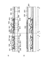
本実施の形態においては、導電膜上に塗れ性の低い材料で形成される第1のマスクパターンを形成した後、塗れ性の高い材料で形成される第2のマスクパターンを形成して、第1のマスクパターンを除去して画素電極を形成するためのマスクパターンを形成する工程、及び画素電極を形成する工程を、図1を用いて説明する。
(Embodiment 1)
In this embodiment, after forming a first mask pattern formed using a material with low wettability over the conductive film, a second mask pattern formed using a material with high wettability is formed, A step of forming a mask pattern for forming a pixel electrode by removing the mask pattern 1 and a step of forming a pixel electrode will be described with reference to FIG.
図1(A)に示すように、基板1001上に第1の導電層1002を成膜する。第1の導電層としては、画素電極として機能することが可能な導電性材料を用いて形成する。
As shown in FIG. 1A, a first
基板1001の代表例としては、ガラス基板、石英基板、アルミナなど絶縁物質で形成される基板、後工程の処理温度に耐え得る耐熱性を有するプラスチック基板、シリコンウェハ、金属板等を用いることができる。この場合、酸化シリコン(SiOx)、窒化シリコン(SiNx)、酸化窒化シリコン(SiOxNy)(x>y)、窒化酸化シリコン(SiNxOy)(x>y)など、基板側から不純物などの拡散を防止するための絶縁膜を形成しておくことが望ましい。また、ステンレスなどの金属または半導体基板などの表面に酸化シリコンや窒化シリコンなどの絶縁膜を形成した基板なども用いることができる。また、基板1001としてガラス基板を用いる場合、320mm×400mm、370mm×470mm、550mm×650mm、600mm×720mm、680mm×880mm、1000mm×1200mm、1100mm×1250mm、1150mm×1300mmのような大面積基板を用いることができる。ここでは、基板1001としてガラス基板を用いる。
As a typical example of the
なお、基板1001にプラスチック基板を用いる場合、PC(ポリカーボネート)、PES(ポリエチレンスルホン)、PET(ポリエチレンテレフタレート)もしくはPEN(ポリエチレンナフタレート)等のガラス転移点が比較的高いものを用いることが好ましい。
Note that when a plastic substrate is used as the
第1の導電層1002の代表的な材料としては、透光性を有する導電膜、又は反射性を有する導電膜がある。透光性を有する導電膜の材料としては、酸化インジウムスズ(ITO)、酸化亜鉛(ZnO)、酸化インジウム亜鉛(IZO)、ガリウムを添加した酸化亜鉛(GZO)、酸化珪素を含む酸化インジウムスズ等が挙げられる。また、反射性を有する導電膜の材料としては、アルミニウム(Al)、チタン(Ti)、銀(Ag)、タンタル(Ta)などの金属、又は該金属と化学量論的組成比以下の濃度で窒素を含む金属材料、若しくは該金属の窒化物である窒化チタン(TiN)、窒化タンタル(TaN)、若しくは1〜20%のニッケルを含むアルミニウムなどが挙げられる。
As a typical material of the first
導電膜1002の形成方法としては、スパッタリング法、蒸着法、CVD法、塗布法等を適宜用いる。
As a method for forming the
次に、図1(B)に示すように、第1の導電層1002上に第1のマスクパターン1003を形成する。第1のマスクパターンは、後に形成する第2のマスクパターン(導電層をエッチングするためマスクとして機能する膜)を形成するためのマスクとして機能する。このため、塗れ性が低いことが好ましい。即ち、第1のマスクパターンの表面において、後に形成する第2のマスクパターンを弾きやすいことが好ましい。
Next, as illustrated in FIG. 1B, a
本実施の形態では、第1のマスクパターン1003の形成方法としては、所定の場所に塗れ性の高い絶縁層を形成し、フッ素プラズマを該表面に曝して形成する。また、誘電体が設けられた電極を用意し、誘電体が空気、酸素又は窒素を用いたプラズマに曝されるようにプラズマを発生させてプラズマ処理を行うことができる。この場合、誘電体は電極表面全体を覆う必要はない。誘電体としては、フッ素樹脂を用いることができる。フッ素樹脂を用いる場合、絶縁層表面にCF2結合が形成されることにより表面改質が行われ、塗れ性が低下する。
In this embodiment mode, as a method for forming the
絶縁層の材料として、ポリビニルアルコール(PVA)のような水溶性樹脂を、H2O等の溶媒に混合した材料を用いることができる。また、PVAと他の水溶性樹脂を組み合わせて使用してもよい。また、アクリル樹脂、ポリイミド樹脂、メラミン樹脂、ポリエステル樹脂、ポリカーボネート樹脂、フェノール樹脂、エポキシ樹脂、ポリアセタール、ポリエーテル、ポリウレタン、ポリアミド(ナイロン)、フラン樹脂、ジアリルフタレート樹脂等の有機樹脂などを用いることができる。 As a material for the insulating layer, a material in which a water-soluble resin such as polyvinyl alcohol (PVA) is mixed with a solvent such as H 2 O can be used. Moreover, you may use combining PVA and another water-soluble resin. In addition, organic resins such as acrylic resin, polyimide resin, melamine resin, polyester resin, polycarbonate resin, phenol resin, epoxy resin, polyacetal, polyether, polyurethane, polyamide (nylon), furan resin, diallyl phthalate resin, etc. may be used. it can.
絶縁層の作製方法としては、スクリーン(孔版)印刷、オフセット(平版)印刷、凸版印刷、及びグラビア(凹版)印刷等に代表される印刷法、並びに液滴吐出法が挙げられ、これらにより所定の領域に形成することができる。 Examples of the method for producing the insulating layer include printing methods represented by screen (stencil printing), offset (lithographic printing) printing, relief printing, gravure printing (intaglio printing), and a droplet discharge method. Can be formed in the region.
なお、液滴吐出法により絶縁層を形成する場合、液滴吐出手段に用いるノズルの径は、0.1〜50μm(好適には0.6〜26μm)に設定し、ノズルから吐出される組成物の吐出量は0.00001pl〜50pl(好適には0.0001〜10pl)に設定する。この吐出量は、ノズルの径の大きさに比例して増加する。また、被処理物とノズル吐出口との距離は、所望の箇所に滴下するために、できる限り近づけておくことが好ましく、好適には0.1〜2cm程度に設定する。 When the insulating layer is formed by the droplet discharge method, the nozzle diameter used for the droplet discharge means is set to 0.1 to 50 μm (preferably 0.6 to 26 μm), and the composition is discharged from the nozzle. The discharge amount of the object is set to 0.00001 pl to 50 pl (preferably 0.0001 to 10 pl). This discharge amount increases in proportion to the size of the nozzle diameter. In addition, the distance between the object to be processed and the nozzle discharge port is preferably as close as possible in order to drop it at a desired location, and is preferably set to about 0.1 to 2 cm.
次に、図1(C)に示すように、第1の導電層1002上であって、且つ第1のマスクパターン1003が形成されていない領域に第2のマスクパターン1004を形成する。第2のマスクパターンとしては、第1のマスクパターンと比較して塗れ性の高い材料を用いて形成する。
Next, as shown in FIG. 1C, a
ここで、図27を用いて塗れ性の低い領域と塗れ性の高い領域の関係について示す。塗れ性の低い領域(ここでは、第1のマスクパターン1003)とは、図27に示すように、表面において液体の接触角θ1が大きい領域である。この表面上では液体は、半球状にはじかれる。一方、塗れ性の高い領域(ここでは、第2のマスクパターン1004)は、表面において液体の接触角θ2が小さい領域である。この表面上では、液体は塗れ広がる。 Here, FIG. 27 is used to show the relationship between a low-paintability region and a high-paintability region. The region with low smearability (here, the first mask pattern 1003) is a region where the liquid contact angle θ1 is large on the surface, as shown in FIG. On this surface the liquid is repelled by a hemisphere. On the other hand, the region with high wettability (here, the second mask pattern 1004) is a region where the liquid contact angle θ2 is small on the surface. On this surface, the liquid spreads and spreads.
このため、接触角の異なる二つの領域が接している場合、相対的に接触角の小さい領域は塗れ性の高い領域となり、接触角の大きい方の領域は塗れ性が低い領域となる。この二つの領域上に組成物を塗布した場合、組成物は、塗れ性が高い領域表面に塗れ広がり、塗れ性が低い領域との界面で半球状にはじかれる。 For this reason, when two regions having different contact angles are in contact with each other, a region having a relatively small contact angle is a region having high paintability, and a region having a larger contact angle is a region having low paintability. When the composition is applied on the two regions, the composition spreads on the surface of the highly wettable region and repels at the interface with the low wettable region.
塗れ性の低い領域の接触角θ1と塗れ性の高い領域の接触角θ2の差は、30度、望ましくは40度以上であることが好ましい。この結果、塗れ性の低い領域の表面で塗れ性の高い領域の材料が半球状にはじかれ、自己整合的に各マスクパターンを形成することが可能である。このため、第1のマスクパターン1003の形成方法及び材料で列挙されたものの中で、互いの接触角の差が30度、望ましくは40度以上の場合、接触角の小さい材料で形成された領域は塗れ性の高い領域となり、接触角の大きい材料で形成された領域は塗れ性の低い領域となる。同様に、これから第2のマスクパターン1004の材料として列挙されるものの中で、互いの接触角の差が30度、望ましくは40度以上の場合、接触角の小さい材料で形成された領域は塗れ性の高い領域となり、接触角の大きい材料で形成された領域は塗れ性の低い領域となる。
The difference between the contact angle θ1 of the low wettability region and the contact angle θ2 of the high wettability region is 30 degrees, preferably 40 degrees or more. As a result, the material of the highly wettable area is repelled on the surface of the low wettable area, and each mask pattern can be formed in a self-aligning manner. For this reason, among the enumerated methods and materials for forming the
なお、表面が凹凸を有する場合、塗れ性が低い領域ではさらに接触角が増加する。即ち、塗れ性がより低下する。一方、塗れ性が高い領域では、さらに接触角が低下する。即ち、塗れ性がより向上する。このため、凹凸を有する各表面上に塗れ性の低い材料と塗れ性の高い材料を塗布し、焼成することにより、端部が均一な層を形成することができる。 In addition, when the surface has an unevenness | corrugation, a contact angle increases further in the area | region where paintability is low. That is, paintability is further reduced. On the other hand, the contact angle is further lowered in the region where the paintability is high. That is, paintability is further improved. For this reason, it is possible to form a layer having uniform end portions by applying a low wettability material and a high wettability material on each surface having unevenness and baking.
第2のマスクパターン1004としては、アクリル樹脂、ポリイミド樹脂、メラミン樹脂、ポリエステル樹脂、ポリカーボネート樹脂、フェノール樹脂、エポキシ樹脂、ポリアセタール、ポリエーテル、ポリウレタン、ポリアミド(ナイロン)、フラン樹脂、ジアリルフタレート樹脂、ノボラック樹脂、珪素樹脂、レジスト等の有機樹脂、シロキサンポリマー、ポリシラザンを用いることができる。また、水、アルコール、エーテル、ジメチルホルムアミド、ジメチルアセトアミド、ジメチルスルホキシド、N−メチルピロリドン、ヘキサメチルホスファミド、クロロホルム、塩化メチレン等の極性溶媒を用いた組成物等の塗れ性の高い材料を用いて形成することができる。また、形成方法としては、塗布法を用いることができる。代表的には、液滴吐出法、インクジェット法、スピンコート法、ロールコート法、スロットコート法、印刷法等を適宜用いる。なお、液滴吐出法を用いることで、選択的に材料を吐出することができるため、所定の領域に第2のマスクパターンを形成することができる。
As the
次に、図1(D)に示すように、第1のマスクパターン1003を除去して、第1の導電層1002の一部1005を露出する。第1のマスクパターン1003の除去方法としては、酸素アッシング、ウェットエッチング法等を適宜用いることができる。
Next, as shown in FIG. 1D, the
次に、図1(E)に示すように、第2のマスクパターン1004をマスクとして第1の導電層1002をエッチングして、所望の形状を有する第2の導電層1006を形成する。
Next, as shown in FIG. 1E, the first
次に、図1(F)に示すように、第2のマスクパターン1004をドライエッチング、ウェットエッチング等の公知の方法により除去することで、第2の導電層1006を露出する。第2の導電層1006は画素電極として用いることができる。
Next, as shown in FIG. 1F, the second
以上の工程により、フォトリソグラフィー工程を用いずとも所望の形状を有する導電層、画素電極を形成することができる。また、パッシブマトリクス型表示装置のマトリクス基板を形成することができる。 Through the above steps, a conductive layer and a pixel electrode having a desired shape can be formed without using a photolithography step. In addition, a matrix substrate of a passive matrix display device can be formed.
(実施の形態2)
本実施の形態では、フッ素炭素鎖を有する化合物を用いて塗れ性の低い材料を用いて第1のマスクパターンを形成した後、塗れ性の高い材料を用いて第2のマスクパターンを形成して、画素電極を形成するマスクパターンを形成する工程と、画素電極を形成する工程を図2を用いて説明する。
(Embodiment 2)
In this embodiment, the first mask pattern is formed using a material having low wettability using a compound having a fluorine carbon chain, and then the second mask pattern is formed using material having high wettability. A process of forming a mask pattern for forming a pixel electrode and a process of forming a pixel electrode will be described with reference to FIG.
図2(A)に示すように、実施の形態1と同様に、基板1001上に第1の導電層1002を形成する。
As shown in FIG. 2A, a first
次に、図2(B)に示すように、第1の導電層1002上に第1のマスクパターン10
11を形成する。本実施の形態では、第1のマスクパターンとしては、塗れ性の低いマスクパターンを形成する。第1のマスクパターン1011の材料としては、スクリーン(孔版)印刷、オフセット(平版)印刷、凸版印刷、及びグラビア(凹版)印刷等に代表される印刷法、並びに液滴吐出法等により塗れ性の低い材料を塗布して形成する。塗れ性の低い材料の組成物の一例としては、Rn−Si−X(4-n)(n=1、2、3)の化学式で表されるシランカップリング剤を用いる。ここで、Rは、アルキル基などの比較的不活性な基である。また、Xは、下地表面の水酸基あるいは吸着水と結合可能な加水分解基からなる。Xの代表例としては、ハロゲン、メトキシ基、エトキシ基又はアセトキシ基などが挙げられる。
Next, as shown in FIG. 2B, the first mask pattern 10 is formed on the first
11 is formed. In the present embodiment, a mask pattern with low wettability is formed as the first mask pattern. As a material of the
また、シランカップリング剤の代表例として、Rにフッ素炭素鎖(フルオロアルキル基)を有するフッ素シランカップリング剤(フルオロアルキルシラン(FAS))を用いることにより、より塗れ性を低下させることができる。FASのRは、(CF3)(CF2)x(CH2)y(x:0以上10以下の整数、y:0以上4以下の整数)で表される構造を持ち、複数個のR又はXがSiに結合している場合には、R又はXはそれぞれすべて同じでも良いし、異なっていてもよい。代表的なFASとしては、ヘプタデカフルオロテトラヒドロデシルトリエトキシシラン、ヘプタデカフルオロテトラヒドロデシルトリクロロシラン、トリデカフルオロテトラヒドロオクチルトリクロロシラン、トリフルオロプロピルトリメトキシシラン等のフルオロアルキルシランが挙げられる。 Moreover, as a typical example of a silane coupling agent, the wettability can be further reduced by using a fluorine silane coupling agent (fluoroalkylsilane (FAS)) having a fluorine carbon chain (fluoroalkyl group) in R. . R of FAS has a structure represented by (CF 3 ) (CF 2 ) x (CH 2 ) y (x: an integer of 0 or more and 10 or less, y: an integer of 0 or more and 4 or less), and a plurality of R Alternatively, when X is bonded to Si, R and X may all be the same or different. Typical FAS includes fluoroalkylsilanes such as heptadecafluorotetrahydrodecyltriethoxysilane, heptadecafluorotetrahydrodecyltrichlorosilane, tridecafluorotetrahydrooctyltrichlorosilane, and trifluoropropyltrimethoxysilane.
塗れ性の低い組成物の溶媒としては、nーペンタン、n−ヘキサン、n−ヘプタン、n−オクタン、n−デカン、ジシクロペンタン、ベンゼン、トルエン、キシレン、デュレン、インデン、テトラヒドロナフタレン、デカヒドロナフタレン、スクワランなどの炭化水素溶媒又はテトラヒドロフランなどを用いる。 As a solvent for a composition having low wettability, n-pentane, n-hexane, n-heptane, n-octane, n-decane, dicyclopentane, benzene, toluene, xylene, durene, indene, tetrahydronaphthalene, decahydronaphthalene , A hydrocarbon solvent such as squalane or tetrahydrofuran is used.
また、塗れ性の低い組成物の一例として、フッ素炭素鎖を有する材料(フッ素樹脂)を用いることができる。フッ素樹脂として、ポリテトラフルオロエチレン(PTFE;四フッ化エチレン樹脂)、パーフルオロアルコキシアルカン(PFA;四フッ化エチレンパーフルオロアルキルビニルエーテル共重合樹脂)、パーフルオロエチレンプロピレンコーポリマー(PFEP;四フッ化エチレン−六フッ化プロピレン共重合樹脂)、エチレン−テトラフルオロエチレンコポリマー(ETFE;四フッ化エチレン−エチレン共重合樹脂)、ポリビニリデンフルオライド(PVDF;フッ化ビニリデン樹脂)、ポリクロロトリフルオロエチレン(PCTFE;三フッ化塩化エチレン樹脂)、エチレン−クロロトリフルオロエチレンコポリマー(ECTFE;三フッ化塩化エチレン−エチレン共重合樹脂)、ポリテトラフルオロエチレン−パーフルオロジオキソールコポリマー(TFE/PDD)、ポリビニルフルオライド(PVF;フッ化ビニル樹脂)等を用いることができる。 In addition, as an example of a composition having low wettability, a material having a fluorocarbon chain (fluororesin) can be used. As fluororesin, polytetrafluoroethylene (PTFE; tetrafluoroethylene resin), perfluoroalkoxyalkane (PFA; tetrafluoroethylene perfluoroalkyl vinyl ether copolymer resin), perfluoroethylene propylene copolymer (PFEP; tetrafluoride). Ethylene-hexafluoropropylene copolymer resin), ethylene-tetrafluoroethylene copolymer (ETFE; tetrafluoroethylene-ethylene copolymer resin), polyvinylidene fluoride (PVDF; vinylidene fluoride resin), polychlorotrifluoroethylene ( PCTFE; trifluorochloroethylene resin), ethylene-chlorotrifluoroethylene copolymer (ECTFE; trifluoroethylene chloride-ethylene copolymer resin), polytetrafluoroethylene-perfluorodioxide Rukoporima (TFE / PDD), polyvinyl fluoride (PVF; a vinyl fluoride resin), or the like can be used.
続いて、塗れ性の低い組成物が付着した表面をエタノール洗浄すると、極めて膜厚が薄く塗れ性の低い第1のマスクパターンを形成することができる。 Subsequently, when the surface to which the composition having low wettability is attached is cleaned with ethanol, the first mask pattern having a very thin film thickness and low wettability can be formed.
次に図2(C)に示すように、第1の導電層1002上であって、且つ第1のマスクパターン1011が形成されていない領域に第2のマスクパターン1012を形成する。第2のマスクパターンの材料及び作製方法は、実施の形態1の第2のマスクパターン1004と同様の物を適宜用いることができる。
Next, as shown in FIG. 2C, a
次に、図2(D)に示すように、実施の形態1と同様に第1のマスクパターン1011を除去して、第1の導電層1002の一部1013を露出する。
Next, as shown in FIG. 2D, the
次に、図2(E)に示すように、第1の実施の形態と同様に第2のマスクパターン1012をマスクとして第1の導電層1002をエッチングして、所望の形状を有する第2の導電層1014を形成する。
Next, as shown in FIG. 2E, the first
次に、図2(F)に示すように、第2のマスクパターン1012を除去することで、第2の導電層1014を露出する。第2の導電層1014は画素電極として用いることができる。
Next, as shown in FIG. 2F, the second
以上の工程により、フォトリソグラフィー工程を用いずとも所望の形状を有する導電層、画素電極を形成することができる。また、パッシブマトリクス型表示装置のマトリクス基板を形成することができる。 Through the above steps, a conductive layer and a pixel electrode having a desired shape can be formed without using a photolithography step. In addition, a matrix substrate of a passive matrix display device can be formed.
(実施の形態3)
本実施の形態では、表示装置のアクティブマトリクス基板の作製方法について図3を用いて説明する。本実施の形態では、画素駆動素子として、ボトムゲートのチャネルエッチ型TFTを用いて説明する。なお、実施の形態1を用いて第2の導電層301を形成するがこれに限定されず、実施の形態2を用いることができる。
(Embodiment 3)
In this embodiment, a method for manufacturing an active matrix substrate of a display device will be described with reference to FIGS. In this embodiment mode, description will be made using a bottom-gate channel etch TFT as a pixel driving element. Note that the second
図3(A)に示すように、基板1001上に第1の導電層1002を成膜する。次に、実施の形態1と同様の工程により、第1のマスクパターン1003を形成した後、第2のマスクパターン1004を形成する。
As shown in FIG. 3A, a first
次に、図3(B)に示すように、第1のマスクパターン1003を除去して、第1の導電層の一部を露出した後、第1の導電層をエッチングして、画素電極として機能する第2の導電層301を形成する。この後、第2のマスクパターン1004を除去する。
Next, as shown in FIG. 3B, the
次に、図3(C)に示すように、ゲート電極として機能する第3の導電層302を基板1001上に形成する。第3の導電層302の材料としては導電性を有する材料を用い、液滴吐出法、印刷法、電界メッキ法、PVD法(Physical Vapor Deposition)、CVD法(Chemical Vapor Deposition)、蒸着法等の作製方法により形成する。なお、PVD法(Physical Vapor Deposition)、CVD法(Chemical Vapor Deposition)、蒸着法等を用いる場合は、上記成膜方法により導電層を成膜した後、所望の形状にエッチングして第3の導電層302を形成する。
Next, as illustrated in FIG. 3C, a third
第3の導電層302の材料としては、Ag、Au、Cu、Ni、Pt、Pd、Ir、Rh、W、Al、Ta、Mo、Cd、Zn、Fe、Ti、Si、Ge、Zr、Ba等の金属、または、透明導電膜として用いられる酸化インジウムスズ(ITO)、酸化亜鉛(ZnO)、酸化インジウム亜鉛(IZO)、ガリウムを添加した酸化亜鉛(GZO)、酸化珪素を含む酸化インジウムスズ、有機インジウム、有機スズ、窒化チタン等適宜用いる。また、これらの材料からなる導電層を積層してもよい。
As the material of the third
また、液滴吐出法で第2の導電層を形成する場合、吐出口から吐出する組成物は、導電体を溶媒に溶解又は分散させたものを用いる。導電体としては、上記導電性を有する材料の金属、ハロゲン化銀の微粒子等、又は分散性ナノ粒子を用いることができる。 In the case where the second conductive layer is formed by a droplet discharge method, a composition in which a conductor is dissolved or dispersed in a solvent is used as the composition discharged from the discharge port. As the conductor, a metal of the above conductive material, silver halide fine particles, or the like, or dispersible nanoparticles can be used.
なお、吐出口から吐出する組成物は、比抵抗値を考慮して、金、銀、銅のいずれかの材料を溶媒に溶解又は分散させたものを用いることが好ましい。より好ましくは、低抵抗且つ安価な銀又は銅を用いるとよい。但し、銅を用いる場合には、不純物対策のため、合わせてバリア膜を設けるとよい。溶媒は、酢酸ブチル、酢酸エチル等のエステル類、イソプロピルアルコール、エチルアルコール等のアルコール類、メチルエチルケトン、アセトン等の有機溶剤等を用いればよい。 In addition, it is preferable to use what dissolved or disperse | distributed the material of either gold | metal | money, silver, and copper in the solvent considering the specific resistance value as the composition discharged from a discharge outlet. More preferably, low resistance and inexpensive silver or copper may be used. However, when copper is used, a barrier film may be provided as a countermeasure against impurities. As the solvent, esters such as butyl acetate and ethyl acetate, alcohols such as isopropyl alcohol and ethyl alcohol, organic solvents such as methyl ethyl ketone and acetone may be used.
ここで、銅を配線として用いる場合のバリア膜としては、窒化シリコン、酸化窒化シリコン、窒化アルミニウム、窒化チタン、窒化タンタルなど窒素を含む絶縁性又は導電性の物質を用いると良く、これらを液滴吐出法で形成しても良い。 Here, an insulating or conductive substance containing nitrogen such as silicon nitride, silicon oxynitride, aluminum nitride, titanium nitride, or tantalum nitride is preferably used as a barrier film in the case of using copper as a wiring. It may be formed by a discharge method.
なお、液滴吐出法に用いる組成物の粘度は5〜20mPa・sが好適であり、これは、乾燥が起こることを防止し、吐出口から組成物を円滑に吐出できるようにするためである。また、表面張力は40mN/m以下が好ましい。なお、用いる溶媒や用途に合わせて、組成物の粘度等は適宜調整するとよい。一例として、ITO、ZnO、IZO、GZO、酸化珪素を含む酸化インジウムスズ、有機インジウム、有機スズ等を溶媒に溶解又は分散させた組成物の粘度は5〜20mPa・s、銀を溶媒に溶解又は分散させた組成物の粘度は5〜20mPa・s、金を溶媒に溶解又は分散させた組成物の粘度は10〜20mPa・sである。 The viscosity of the composition used for the droplet discharge method is preferably 5 to 20 mPa · s, which is to prevent the drying from occurring and to smoothly discharge the composition from the discharge port. . The surface tension is preferably 40 mN / m or less. Note that the viscosity of the composition may be appropriately adjusted according to the solvent to be used and the application. As an example, the viscosity of a composition in which ITO, ZnO, IZO, GZO, indium tin oxide containing silicon oxide, organic indium, organic tin, or the like is dissolved or dispersed in a solvent is 5 to 20 mPa · s, or silver is dissolved in the solvent. The viscosity of the dispersed composition is 5 to 20 mPa · s, and the viscosity of the composition in which gold is dissolved or dispersed in a solvent is 10 to 20 mPa · s.
各ノズルの径や所望のパターン形状などに依存するが、ノズルの目詰まり防止や高精細なパターンの作製のため、導電体の粒子の径はなるべく小さい方が好ましく、好適には粒径0.1μm以下が好ましい。組成物は、電解法、アトマイズ法又は湿式還元法等の公知の方法で形成されるものであり、その粒子サイズは、一般的に約0.5〜10μmである。ただし、ガス中蒸発法で形成すると、分散剤で保護されたナノ粒子は約7nmと微細であり、またこのナノ粒子は、被覆剤を用いて各粒子の表面を覆うと、溶剤中に凝集がなく、室温で安定に分散し、液体とほぼ同じ挙動を示す。したがって、被覆剤を用いることが好ましい。 Although depending on the diameter of each nozzle and the desired pattern shape, the diameter of the conductor particles is preferably as small as possible for preventing nozzle clogging and producing a high-definition pattern. 1 μm or less is preferable. The composition is formed by a known method such as an electrolytic method, an atomizing method, or a wet reduction method, and its particle size is generally about 0.5 to 10 μm. However, when formed by the gas evaporation method, the nanoparticles protected with the dispersant are as fine as about 7 nm. When the nanoparticles are covered with a coating agent, the nanoparticles are aggregated in the solvent. And stably disperse at room temperature and shows almost the same behavior as liquid. Therefore, it is preferable to use a coating agent.
組成物を吐出する工程は、減圧下で行っても良い。これは、組成物を吐出して被処理物に着弾するまでの間に、該組成物の溶媒が揮発し、後の乾燥と焼成の工程を省略又は短くすることができるためである。組成物の吐出後は、組成物の材料により、常圧下又は減圧下で、レーザ光の照射や瞬間熱アニール、加熱炉等により、乾燥と焼成の一方又は両方の工程を行う。乾燥と焼成の工程は、両工程とも加熱処理の工程であるが、例えば、乾燥は100度で3分間、焼成は200〜350度で15分間〜120分間で行うもので、その目的、温度と時間が異なるものである。乾燥と焼成の工程を良好に行うためには、基板を加熱しておいてもよく、そのときの温度は、基板等の材質に依存するが、100〜800度(好ましくは200〜350度)とする。本工程により、組成物中の溶媒を揮発させ、又は化学的に分散剤を除去し、組成物の樹脂が硬化収縮することで、導電体の融合と融着を加速する。本工程は、酸素雰囲気、窒素雰囲気又は空気雰囲気で行う。特に、組成物の溶媒が除去されやすい酸素雰囲気下で行うことが好適であるが、加熱温度、雰囲気、時間により該導電層には、有機物で形成されるバインダーが残存する。 The step of discharging the composition may be performed under reduced pressure. This is because the solvent of the composition volatilizes before the composition is discharged and landed on the object to be processed, and the subsequent drying and firing steps can be omitted or shortened. After discharging the composition, one or both of drying and baking processes are performed by laser light irradiation, rapid thermal annealing, a heating furnace, or the like under normal pressure or reduced pressure depending on the material of the composition. The drying and firing steps are both heat treatment steps. For example, the drying is performed at 100 degrees for 3 minutes, and the firing is performed at 200 to 350 degrees for 15 minutes to 120 minutes. Time is different. In order to satisfactorily perform the drying and firing steps, the substrate may be heated, and the temperature at that time depends on the material of the substrate or the like, but is 100 to 800 degrees (preferably 200 to 350 degrees). And By this step, the solvent in the composition is volatilized or the dispersant is chemically removed, and the resin of the composition is cured and contracted to accelerate the fusion and fusion of the conductors. This step is performed in an oxygen atmosphere, a nitrogen atmosphere, or an air atmosphere. In particular, it is preferable to perform in an oxygen atmosphere in which the solvent of the composition is easily removed. However, a binder formed of an organic substance remains in the conductive layer depending on the heating temperature, atmosphere, and time.
本実施の形態では、第3の導電層302は、数nmの銀粒子が分散された組成物(以下「Agペースト」という。)を選択的に吐出し、乾燥焼成して、銀を主成分とする導電層を形成する。なお、第3の導電層は、導電体である微粒子が3次元に不規則に重なり合って形成されている。このため、表面は微細な凹凸を有する。また、第3の導電層302の加熱温度及びその加熱時間により、複数の微粒子が焼成され粒子の粒径が増大するため、第3の導電層302の表面の高低差が大きい層となる。
In this embodiment mode, the third
次に、第2の導電層301及び第3の導電層302上にゲート絶縁膜として機能する第1の絶縁層303、第1の半導体膜304、導電性を有する第2の半導体膜305を形成する。第1の絶縁層303はプラズマCVD法またはスパッタリング法などの薄膜形成法を用い、窒化シリコン、酸化シリコン、その他の珪素を含む絶縁膜の単層又は積層構造で形成する。また、第1の絶縁層をゲート電極に接する側から、窒化珪素膜(窒化酸化珪素膜)、酸化珪素膜、及び窒化珪素膜(窒化酸化珪素膜)の積層構造とすることが好ましい。この構造では、ゲート電極が、窒化珪素膜と接しているため、酸化による劣化を防止することができる。
Next, a first insulating
また、第1の絶縁層303を、液滴吐出法、インクジェット法、スピンコート法、ロールコート法、スロットコート法、ゾルゲル法、又はディップ法に代表される塗布法を用いて絶縁性を有する組成物を用いて形成することができる。絶縁性を有する組成物の代表例としては、無機酸化物の微粒子が分散された組成物、ポリイミド、ポリアミド、ポリエステル、アクリル、PSG(リンガラス)、BPSG(リンボロンガラス)、シリケートSOG(Spin on Glass)、アルコキシシリケートSOG、ポリシラザンSOG、シロキサンポリマー等を適宜用いることができる。
In addition, the first insulating
第1の半導体膜304としては、非晶質半導体、非晶質状態と結晶状態とが混在したセミアモルファス半導体(SASとも表記する)、非晶質半導体中に0.5nm〜20nmの結晶粒を観察することができる微結晶半導体、及び結晶性半導体から選ばれたいずれの状態を有する膜で形成する。特に、0.5nm〜20nmの結晶を粒観察することができる微結晶状態はいわゆるマイクロクリスタル(μc)と呼ばれている。いずれも、シリコン、シリコン・ゲルマニウム(SiGe)等を主成分とし、膜厚が10〜60nmの半導体膜を用いることができる。
As the
SASは、非晶質構造と結晶構造(単結晶、多結晶を含む)との中間的な構造を有し、自由エネルギー的に安定な第3の状態を有する半導体である。また短距離秩序を持ち格子歪みを有する結晶質な領域を含んでいる。そして少なくとも膜中の一部の領域には、0.5〜20nmの結晶領域を観測することができ、珪素を主成分とする場合にはラマンスペクトルが520cm-1よりも低波数側にシフトしている。X線回折では珪素結晶格子に由来するとされる(111)、(220)の回折ピークが観測される。また未結合手(ダングリングボンド)の終端化として、SASは水素或いはハロゲンを1原子%、又はそれ以上含んでいる。 The SAS is a semiconductor having an intermediate structure between an amorphous structure and a crystal structure (including single crystal and polycrystal) and having a third state that is stable in terms of free energy. It also contains a crystalline region with short-range order and lattice distortion. A crystal region of 0.5 to 20 nm can be observed in at least a part of the film, and when silicon is the main component, the Raman spectrum shifts to a lower wave number side than 520 cm −1. ing. In X-ray diffraction, diffraction peaks of (111) and (220) that are derived from the silicon crystal lattice are observed. As a termination of dangling bonds, SAS contains 1 atomic% or more of hydrogen or halogen.
SASは、珪化物気体をグロー放電分解することにより得ることができる。代表的な珪化物気体としては、SiH4であり、その他にもSi2H6、SiH2Cl2、SiHCl3、SiCl4、SiF4などを用いることができる。珪化物気体を水素又はフッ素、若しくは水素又はフッ素とヘリウム、アルゴン、クリプトン、ネオンから選ばれた一種又は複数種の希ガス元素とで希釈して用いることにより、SASの形成を容易なものとすることができる。このとき希釈率が10倍〜1000倍の範囲となるように、珪化物気体を希釈すると好ましい。またSi2H6及びGeF4を用い、ヘリウムガスで希釈する方法を用いてSASを形成することができる。グロー放電分解による被膜の反応生成は減圧下で行うと好ましく、圧力は概略0.1Pa〜133Paの範囲で行えばよい。グロー放電を形成するための電力は1MHz〜120MHz、好ましくは13MHz〜60MHzの高周波電力を供給すればよい。基板加熱温度は300度以下が好ましく、100〜250度の基板加熱温度が推奨される。 SAS can be obtained by glow discharge decomposition of a silicide gas. A typical silicide gas is SiH 4 , and in addition, Si 2 H 6 , SiH 2 Cl 2 , SiHCl 3 , SiCl 4 , SiF 4 and the like can be used. By forming a silicide gas diluted with hydrogen or fluorine, or hydrogen or fluorine and one or more kinds of rare gas elements selected from helium, argon, krypton, and neon, the formation of SAS is facilitated. be able to. At this time, it is preferable to dilute the silicide gas so that the dilution rate is in the range of 10 to 1000 times. Further, the SAS can be formed by using Si 2 H 6 and GeF 4 and diluting with helium gas. The reaction generation of the coating by glow discharge decomposition is preferably performed under reduced pressure, and the pressure may be in the range of about 0.1 Pa to 133 Pa. The power for forming the glow discharge may be high frequency power of 1 MHz to 120 MHz, preferably 13 MHz to 60 MHz. The substrate heating temperature is preferably 300 ° C. or less, and a substrate heating temperature of 100 to 250 ° C. is recommended.
また、結晶性半導体膜は、非晶質半導体膜又はSASを、加熱又はレーザ照射により結晶化して形成することができる。また、直接、結晶性半導体膜を形成してもよい。この場合、GeF4、又はF2等のフッ素ガスと、SiH4、又はSi2H6等のシランガスとを用い、熱又はプラズマを利用して直接結晶性半導体膜を形成することができる。 The crystalline semiconductor film can be formed by crystallizing an amorphous semiconductor film or SAS by heating or laser irradiation. Alternatively, a crystalline semiconductor film may be directly formed. In this case, the crystalline semiconductor film can be directly formed using heat or plasma using a fluorine gas such as GeF 4 or F 2 and a silane gas such as SiH 4 or Si 2 H 6 .
第2の半導体膜305は導電性を有する。nチャネル型のTFTを形成する場合には、15属の元素、代表的にはリンまたはヒ素を添加する。また、pチャネルTFTを形成する場合には、13属の元素、代表的にはボロンを添加する。第2の半導体膜は、珪化物気体にボロン、リン、ヒ素のような13属又は15属の元素を有する気体を加えたプラズマCVD法で成膜する。また、半導体膜を成膜したのち、13属または15属の元素を有する組成物を半導体膜上に塗布しレーザビームを照射して導電性を有する第2の半導体膜を形成することができる。レーザビームとしては、公知のパルス発振のレーザ又は連続発振のレーザから射出されるレーザビームを適宜用いる。
The
次に、第2の半導体膜305上に第3のマスクパターン306を形成する。第3のマスクパターンは、耐熱性高分子材料を用いて形成することが好ましく、芳香環又は複素環を主鎖にもち、脂肪族部分に少なくとも高極性のヘテロ原子基を含む高分子を液滴吐出により吐出して形成することが好ましい。そのような高分子物質の代表例としてはポリイミド又はポリベンゾイミダゾールなどが挙げられる。ポリイミドを用いる場合には、ポリイミドを含む組成物を、吐出口から第2の半導体膜305上に吐出し、200℃で30分焼成して形成することができる。
Next, a
次に、第3のマスクパターン306を用いて第2の半導体膜305をエッチングし、図3(D)に示す第1の半導体領域(ソース領域及びドレイン領域、コンタクト層ともいう。)311を形成する。この後、第3のマスクパターンを除去する。
Next, the
第1の半導体膜は、Cl2、BCl3、SiCl4もしくはCCl4などを代表とする塩素ガス、CF4、SF6、NF3、CHF3などを代表とするフッ素ガス、あるいはO2を用いてエッチングすることができる。 The first semiconductor film uses chlorine gas typified by Cl 2 , BCl 3 , SiCl 4, CCl 4, etc., fluorine gas typified by CF 4 , SF 6 , NF 3 , CHF 3, etc., or O 2 . Can be etched.
次に第1の半導体領域311及びその間の第1の半導体膜304上に、第4のマスクパターン312を形成する。第4のマスクパターンは、第3のマスクパターンと同様の材料を用いて形成することができる。
Next, a fourth mask pattern 312 is formed over the
次に、第4のマスクパターン312をマスクとして、第1の半導体膜304をエッチングして、図3(E)に示す第2の半導体領域(チャネル形成領域)313を形成する。第2の半導体膜のエッチング条件は、第1の半導体膜のエッチング条件を適用することができる。この後、第4のマスクパターンを、剥離液を用いた処理又は酸素を用いたアッシング処理等により除去する。
Next, using the fourth mask pattern 312 as a mask, the
なお、第2の半導体領域313を、有機半導体材料を用い、印刷法、液滴吐出法などで形成することができる。この場合、上記エッチング工程が必要ないため、工程数を削減することが可能である。本発明に用いる有機半導体材料としては、その骨格が共役二重結合から構成されるπ電子共役の高分子材料が望ましい。代表的には、ポリチオフェン、ポリ(3−アルキルチオフェン)、ポリチオフェン誘導体、ペンタセン等の可溶性の高分子材料を用いることができる。
Note that the
その他にも本発明に用いることができる有機半導体材料としては、可溶性の前駆体を成膜した後で処理することにより第2の半導体領域を形成することができる材料がある。なお、このような前駆体を用いて形成する有機半導体材料としては、ポリチエニレンビニレン、ポリ(2,5−チエニレンビニレン)、ポリアセチレン、ポリアセチレン誘導体、ポリアリレンビニレンなどがある。 In addition, as an organic semiconductor material that can be used in the present invention, there is a material that can form a second semiconductor region by processing after forming a soluble precursor. Note that examples of the organic semiconductor material formed using such a precursor include polythienylene vinylene, poly (2,5-thienylene vinylene), polyacetylene, a polyacetylene derivative, and polyarylene vinylene.
前駆体を有機半導体に変換する際には、加熱処理だけではなく塩化水素ガスなどの反応触媒を添加してもよい。これらの可溶性有機半導体材料を溶解させる代表的な溶媒としては、トルエン、キシレン、クロロベンゼン、ジクロロベンゼン、アニソール、クロロホルム、ジクロロメタン、γブチルラクトン、ブチルセルソルブ、シクロヘキサン、NMP(N−メチル−2−ピロリドン)、シクロヘキサノン、2−ブタノン、ジオキサン、ジメチルホルムアミド(DMF)または、THF(テトラヒドロフラン)などを適用することができる。 When converting the precursor into an organic semiconductor, a reaction catalyst such as hydrogen chloride gas may be added in addition to the heat treatment. Typical solvents for dissolving these soluble organic semiconductor materials include toluene, xylene, chlorobenzene, dichlorobenzene, anisole, chloroform, dichloromethane, γ-butyllactone, butyl cellosolve, cyclohexane, NMP (N-methyl-2-pyrrolidone). ), Cyclohexanone, 2-butanone, dioxane, dimethylformamide (DMF), THF (tetrahydrofuran), or the like can be applied.
なお、第2の半導体領域313に有機半導体を用いた場合、第1の半導体領域311の代わりに、ポリアセチレン、ポリアニリン、PEDOT(poly−ethlyenedioxythiophen)、PSS(poly−styrenesulphonate)のような有機導電性材料で形成される導電層を形成することができる。
Note that in the case where an organic semiconductor is used for the
また、第1の半導体領域311の代わりに、金属元素で形成される導電層を用いることができる。この場合、多くの有機半導体材料がキャリアとして正孔を輸送するp型半導体であることからその半導体層とオーミック接触を取るために仕事関数の大きい金属を用いることが望ましい。
Further, a conductive layer formed using a metal element can be used instead of the
具体的には、金や白金、クロム、パラジウム、アルミニウム、インジウム、モリブデン、ニッケル等の金属又は合金等が望ましい。これらの金属又は合金を用いた導電性ペーストを用いて印刷法や液滴吐出法で形成することができる。 Specifically, metals or alloys such as gold, platinum, chromium, palladium, aluminum, indium, molybdenum, and nickel are desirable. It can be formed by a printing method or a droplet discharge method using a conductive paste using these metals or alloys.
さらには、有機半導体材料で形成される第2の半導体領域、有機導電性材料で形成される導電層、及び金属元素で形成される導電層を積層してもよい。 Furthermore, a second semiconductor region formed of an organic semiconductor material, a conductive layer formed of an organic conductive material, and a conductive layer formed of a metal element may be stacked.
なお、第2の半導体領域がSASで形成されている場合、本実施の形態のように、ソース領域及びドレイン領域がゲート電極を覆っている構造のほかに、ソース領域及びドレイン領域の端部とゲート電極の端部が一致しているいわゆるセルフアライン構造とすることができる。さらには、ソース領域及びドレイン領域がゲート電極を覆わず、一定の距離を隔てて形成されている構造とすることができる。この構造の場合、オフ電流を低減することができるため、該TFTを表示装置のスイッチング素子として用いた場合、コントラストを向上させることができる。さらに、第2の半導体領が域複数のゲート電極を覆ういわゆるマルチゲート構造のTFTとしても良い。この場合も、オフ電流を低減することができる。 Note that in the case where the second semiconductor region is formed of SAS, in addition to the structure in which the source region and the drain region cover the gate electrode as in the present embodiment, the end portions of the source region and the drain region A so-called self-aligned structure in which the end portions of the gate electrodes coincide can be obtained. Furthermore, a structure in which the source region and the drain region are formed at a certain distance without covering the gate electrode can be employed. In this structure, off-state current can be reduced, so that contrast can be improved when the TFT is used as a switching element of a display device. Furthermore, a TFT having a so-called multi-gate structure in which the second semiconductor region covers a plurality of gate electrodes may be used. Also in this case, the off current can be reduced.
次に、図3(F)に示すような開口部321を形成する。開口部の形成方法としては、公知のフォトリソグラフィー工程、液滴吐出法を用いて形成したマスクパターンを用いるエッチング法等を適宜用いる。ここでは、図3(E)に示すように、第2の導電層301及び第1の絶縁層303が重畳する領域の一部において、第5のマスクパターン314を形成し、第5のマスクパターンの外縁に第6のマスクパターン315を形成する。第5のマスクパターンは、後に開口部を形成する領域に形成する。第5のマスクパターンとしては、第1のマスクパターンと同様の方法を適宜用いて、塗れ性の低い材料を所定の領域に形成する。また、第6のマスクパターンは第2のマスクパターンと同様の方法を用いて、塗れ性の高い材料を吐出して形成する。次に、第5のマスクパターンを除去して第1の絶縁層303の一部を露出する。次に、第6のマスクパターンを用いて、第1の絶縁層303の露出した領域を除去して、第2の導電層301の一部を露出すると共に、図3(F)に示すような開口部321を形成する。
Next, an
次に、第1の半導体領域311上にソース電極及びドレイン電極として機能する第4の導電層322、323を、導電性材料を用いて形成する。このとき、第4の導電層の一方(図3(E)においては、第4の導電層323)と第1の導電層とが、開口部321において接続する。第4の導電層は、第3の導電層と同様の材料及び形成方法を用いて形成することができる。ここでは、液滴吐出法により数nmの銀粒子が分散された組成物Agペーストを選択的に吐出し、乾燥させて、第4の導電層322、323を形成する。
Next, fourth
次に、第4の導電層322、323上に、パッシベーション膜を成膜することが好ましい。パッシベーション膜は、プラズマCVD法又はスパッタリング法などの薄膜形成法を用い、窒化珪素、酸化珪素、窒化酸化珪素、酸化窒化珪素、酸化窒化アルミニウム、または酸化アルミニウム、ダイアモンドライクカーボン(DLC)、窒素含有炭素(CN)、その他の絶縁性材料を用いて形成することができる。
Next, a passivation film is preferably formed over the fourth
以上の工程により、表示装置のアクティブマトリクス基板を歩留まり高く作製することができる。 Through the above steps, an active matrix substrate of a display device can be manufactured with high yield.
(実施の形態4)
本実施の形態では、表示装置のアクティブマトリクス基板の作製方法について図4を用いて説明する。本実施の形態では、画素駆動素子としてボトムゲートのチャネル保護型TFTを用いて説明する。なお、実施の形態1を用いて第2の導電層301を形成するがこれに限定されず、実施の形態2を用いることができる。
(Embodiment 4)
In this embodiment, a method for manufacturing an active matrix substrate of a display device will be described with reference to FIGS. In this embodiment mode, description is made using a channel protection type TFT having a bottom gate as a pixel driving element. Note that the second
図4(A)及び図4(B)に示すように、実施の形態3と同様の工程により基板1001上に画素電極として機能する第2の導電層301を形成する。この後、第2のマスクパターン1004を除去する。
As shown in FIGS. 4A and 4B, a second
次に、図4(C)に示すように、実施の形態3と同様に、基板1001上にゲート電極として機能する第3の導電層302を形成した後、第2の導電層301及び第3の導電層302上にゲート絶縁膜として機能する第1の絶縁層303、第1の半導体膜304を形成する。次に、第1の半導体膜304上であって、且つ第3の導電層302に重畳する領域に保護膜401を形成する。保護膜401の形成方法及び材料は、実施の形態3に示す第3のマスクパターン306と同様のものを用いることができる。
Next, as illustrated in FIG. 4C, as in Embodiment 3, after the third
次に、第2の半導体膜(導電性を有する半導体膜)405を成膜する。なお、第2の半導体膜405は、実施の形態3の第2の半導体膜305と同様の材料及び作製方法により形成することができる。次に、第3のマスクパターン406を形成する。第3のマスクパターン406は、実施の形態3の第3のマスクパターン306と同様の材料及び形成方法に形成する。
Next, a second semiconductor film (a semiconductor film having conductivity) 405 is formed. Note that the
次に、第3のマスクパターンを用いて、図4(D)に示すように、第1の半導体膜および第2の半導体膜をエッチングし、第1の半導体領域411及び第2の半導体領域413を形成する。この後、第3のマスクパターンを除去する。次に、実施の形態3と同様に開口部321を形成する。
Next, as shown in FIG. 4D, the
次に、図4(E)に示すように、第1の半導体領域411及び開口部321上にソース電極及びドレイン電極として機能する第4の導電層422を、導電性材料を用いて形成する。次に、第4の導電層422をマスクとして、第1の半導体領域411の露出部をエッチングして分断してソース領域及びドレイン領域412を形成する。この工程により、保護膜401が露出される。
Next, as illustrated in FIG. 4E, a fourth
なお、ソース領域及びドレイン領域の形成方法は、本実施の形態に限られず実施の形態3に示される第1の半導体領域の作製工程を用いても良い。また、本実施の形態のソース領域及びドレイン領域の形成工程を実施の形態3に適用しても良い。 Note that the method for forming the source region and the drain region is not limited to this embodiment mode, and the manufacturing process of the first semiconductor region described in Embodiment Mode 3 may be used. In addition, the formation process of the source region and the drain region of this embodiment may be applied to Embodiment 3.
以上の工程により、表示装置のアクティブマトリクス基板を歩留まり高く作製することができる。 Through the above steps, an active matrix substrate of a display device can be manufactured with high yield.
(実施の形態5)
本実施の形態においては、トップゲートの順スタガ型TFTを用いた表示装置のアクティブマトリクス基板の作製方法について、図5を用いて説明する。なお、実施の形態1を用いて第2の導電層301を形成するがこれに限定されず、実施の形態2を用いることができる。
(Embodiment 5)
In this embodiment mode, a method for manufacturing an active matrix substrate of a display device using a top-gate forward staggered TFT will be described with reference to FIGS. Note that the second
図5(A)及び図5(B)に示すように、実施の形態3と同様の工程により基板1001上に画素電極として機能する第2の導電層301を形成する。この後、第2のマスクパターン1004を除去する。
As shown in FIGS. 5A and 5B, a second
次に、図5(C)に示すように、基板1001上にソース電極及びドレイン電極として機能する第3の導電層501、502を形成する。この材料及び作製方法は、実施の形態3の第3の導電層302と同様のものを適宜用いることができる。なお、第3の導電層の一方は、第2の導電層301と接続するように形成する。ここでは、第3の導電層502と第2の導電層301が接続している。
Next, as illustrated in FIG. 5C, third
次に、第3の導電層上に導電性を有する第1の半導体領域503、504を成膜する。第1の半導体領域503、504は、実施の形態3の第1の半導体領域311と同様の材料及び作製方法を適宜用いる。ここでは、液滴吐出法により、有機導電性材料を所定の場所に吐出して第1の半導体領域を形成する。なお、第1の半導体領域は、ソース領域及びドレイン領域として機能する。
Next, conductive
次に、第2の半導体領域505を形成する。
Next, a
次に、図5(D)に示すように、第1の絶縁層506、第4の導電層507を形成する。第1の絶縁層506はゲート絶縁膜として機能するため、実施の形態3の第1の絶縁層303と同様の材料及び形成工程により形成する。また、第4の導電層507はゲート電極として機能するため、実施の形態3の第3の導電層302と同様の材料及び方法で形成する。
Next, as illustrated in FIG. 5D, a first insulating
以上の工程により、表示装置のアクティブマトリクス基板を歩留まり高く作製することができる。 Through the above steps, an active matrix substrate of a display device can be manufactured with high yield.
(実施の形態6)
本発明のトップゲートのコプレナー型TFTを用いた表示装置のアクティブマトリクス基板の作製方法について、図6を用いて説明する。なお、実施の形態1を用いて第3の導電層615を形成するがこれに限定されず、実施の形態2を用いることができる。
(Embodiment 6)
A method for manufacturing an active matrix substrate of a display device using the top gate coplanar TFT of the present invention will be described with reference to FIGS. Note that the third
図6(A)に示すように、基板1001上に第1の絶縁層601を成膜する。第1の絶縁層601は、基板からの不純物が後に形成される半導体領域に拡散するのを防止するためのブロッキング膜として機能する。このため、第1の絶縁層601としては、酸化シリコン膜、窒化シリコン膜または酸化窒化シリコン膜などの絶縁膜から成る下地膜を形成する。下地膜は単層膜または2層以上積層させた構造で形成する。
As shown in FIG. 6A, a first insulating
次に、第1の絶縁層601上に半導体領域602を形成する。半導体領域は、非晶質構造を有する半導体膜を公知の手段(スパッタリング法、LPCVD法、またはプラズマCVD法等)により成膜した後、公知の結晶化処理(パルス発振のレーザから射出されるレーザ光を用いたレーザ結晶化法、熱結晶化法、またはニッケルなどの金属触媒を用いた熱結晶化法等)を行って得られた結晶質半導体膜、又は実施の形態3で示したSAS、AS等をフォトリソグラフィー工程によりパターニングし、エッチングして形成する。
Next, a
また、レーザ結晶化法として、連続発振のレーザを用いてもよい。この場合、非晶質半導体膜の結晶化に際し、大粒径に結晶を得るためには、連続発振が可能な固体レーザを用い、基本波の第2高調波〜第4高調波を適用するのが好ましい。代表的には、Nd:YVO4レーザ(基本波1064nm)の第2高調波(532nm)や第3高調波(355nm)を適用すればよい。連続発振のレーザを用いる場合には、出力10Wの連続発振のYVO4レーザから射出されたレーザ光を非線形光学素子により高調波に変換する。また、共振器の中にYVO4結晶と非線形光学素子を入れて、高調波を射出する方法もある。そして、好ましくは光学系により照射面にて矩形状または楕円形状のレーザ光に成形して、被処理体に照射する。このときのエネルギー密度は0.01〜100MW/cm2程度(好ましくは0.1〜10MW/cm2)が必要である。そして、10〜200cm/s程度の速度でレーザ光に対して相対的に半導体膜を移動させて照射すればよい。この半導体領域の厚さは25〜150nm(好ましくは30〜80nm)の厚さで形成する。結晶質半導体膜の材料に限定はないが、シリコン、ゲルマニウム、またはシリコン・ゲルマニウム(SiGe)合金などで形成すると良い。 As a laser crystallization method, a continuous wave laser may be used. In this case, in order to obtain a crystal having a large grain size when crystallizing the amorphous semiconductor film, a solid-state laser capable of continuous oscillation is used and the second to fourth harmonics of the fundamental wave are applied. Is preferred. Typically, a second harmonic (532 nm) or a third harmonic (355 nm) of an Nd: YVO 4 laser (fundamental wave 1064 nm) may be applied. In the case of using a continuous wave laser, laser light emitted from a continuous wave YVO 4 laser having an output of 10 W is converted into a harmonic by a non-linear optical element. There is also a method of emitting harmonics by putting a YVO 4 crystal and a nonlinear optical element in a resonator. Then, it is preferably formed into a rectangular or elliptical laser beam on the irradiation surface by an optical system, and irradiated to the object to be processed. At this time, the energy density of approximately 0.01 to 100 MW / cm 2 (preferably 0.1 to 10 MW / cm 2) is required. Then, irradiation may be performed by moving the semiconductor film relative to the laser light at a speed of about 10 to 200 cm / s. The semiconductor region is formed to a thickness of 25 to 150 nm (preferably 30 to 80 nm). There is no limitation on the material of the crystalline semiconductor film, but it may be formed of silicon, germanium, a silicon-germanium (SiGe) alloy, or the like.
また、実施の形態3の第2の半導体領域313の材料で列挙した有機半導体材料を用いても良い。
Alternatively, the organic semiconductor materials listed for the material of the
次に、半導体領域602及び第1の絶縁層601上にゲート絶縁膜として機能する第2の絶縁層603を成膜する。第2の絶縁層603としては、実施の形態3に示した第1の絶縁層303と同様の材料及び作製方法を用いて形成することができる。
Next, a second insulating
次に、ゲート電極として機能する第1の導電層604を形成する。第1の導電層としては、実施の形態3に示す第3の導電層302と同様の材料を用いて形成する。作製方法としては、実施の形態3に示す工程のほかに、ICPエッチング装置を用い、テーパ状の端部(テーパー部)を有する導電層としてもよい。テーパー部の角度(テーパー角)は基板表面(水平面)とテーパー部の傾斜部とのなす角度として定義する。導電層のテーパー角は、エッチング条件を適宜、選択することによって、5〜45度の範囲とすることができる。
Next, a first
次に、図6(B)に示すように、第1の導電層604をマスクとして半導体領域602に不純物を添加する。次に、水素を含む絶縁膜を成膜した後、400〜550度に加熱して半導体領域に添加された不純物元素の活性化し、また半導体領域の水素化を行って、不純物領域(ソース領域及びドレイン領域)611、612を形成する。なお、活性化又は水素化の工程として、加熱処理の代わりに、GRTA法、LRTA法、レーザー・アニール法を用いることもできる。加えて、結晶化を助長する金属元素、代表的にはニッケルを用いて半導体膜を結晶化させている場合、活性化と同時にゲッタリングを行うことができる。
Next, as shown in FIG. 6B, an impurity is added to the
なお、本実施の形態では、シングルゲート構造のTFTを示したが、これに限らずマルチゲート構造のものでもよい。また、セルフアライン構造のTFTを示したが、これに限らず低濃度ドレイン(LDD:Lightly Doped Drain)構造若しくはGOLD(Gate−drain Overlapped LDD)構造のTFTを用いることができる。LDD構造は、チャネル形成領域と、高濃度に不純物元素を添加して形成するソース領域またはドレイン領域との間に低濃度に不純物元素を添加した領域を設けたものであり、この領域をLDD領域と呼んでいる。この構造のTFTは、オフ電流値を低減することができる。GOLD構造は、ゲート絶縁膜を介してLDD領域をゲート電極と重ねて配置させた構造であり、ドレイン近傍の電界を緩和してホットキャリア注入による劣化を防ぐ効果がある。 Note that although a single-gate TFT is shown in this embodiment mode, the present invention is not limited to this, and a multi-gate TFT may be used. Although a self-aligned TFT is shown, a TFT having a lightly doped drain (LDD) structure or a GOLD (Gate-drain Overlapped LDD) structure can be used. In the LDD structure, a region to which an impurity element is added at a low concentration is provided between a channel formation region and a source region or a drain region formed by adding an impurity element at a high concentration. It is called. A TFT having this structure can reduce an off-current value. The GOLD structure is a structure in which an LDD region is disposed so as to overlap with a gate electrode through a gate insulating film, and has an effect of relaxing an electric field near the drain and preventing deterioration due to hot carrier injection.
次に、基板上に第2の絶縁層613を形成する。第2の絶縁層の材料としては、酸化珪素、窒化珪素、酸化窒化珪素、酸化アルミニウム、窒化アルミニウム、酸窒化アルミニウムその他の無機絶縁性材料、又はアクリル酸、メタクリル酸及びこれらの誘導体、又はポリイミド(polyimide)、芳香族ポリアミド、ポリベンゾイミダゾール(polybenzimidazole)などの耐熱性高分子、又はシリカガラスに代表されるシロキサンポリマー材料を出発材料として形成された珪素、酸素、水素からなる化合物のうちSi−O−Si結合を含む無機シロキサンポリマー、アルキルシロキサンポリマー、アルキルシルセスキオキサンポリマー、水素化シルセスキオキサンポリマー、水素化アルキルシルセスキオキサンポリマーに代表される珪素に結合する水素がメチルやフェニルのような有機基によって置換された有機シロキサンポリマーの絶縁材料を用いることができる。形成方法としては、CVD法、塗布法、印刷法等公知の手法を用いて形成する。なお、スピンコート法、ロールコート法、スロットコート法に代表される塗布法で形成することにより、第2の絶縁層の表面を平坦化することが可能であり、後の画素電極を形成するためのマスクを形成する工程に適している。ここでは、塗布法により第2の絶縁層613を形成する。
Next, a second insulating
次に、図6(C)に示すように、第2の絶縁層613上に第2の導電層614を形成する。第2の導電層614は実施の形態1に示す第1の導電層1002と同様の材料及び方法により形成する。次に、第2の導電層614上に塗れ性の低い材料を用いて第1のマスクパターン1003を形成した後、第2のマスクパターン1004を形成する。次に、第1のマスクパターンを除去して第2の導電層614の一部を露出した後、第2のマスクパターンを用いて第2の導電層614をエッチングして、図6(D)に示すような第3の導電層615を形成する。次に、フォトリソグラフィー工程及びエッチング工程により、第2の絶縁層613及び第1の絶縁層603の一部を除去して、半導体領域の不純物領域611、612の一部を露出して、開口部621、622を形成する。
Next, as illustrated in FIG. 6C, the second
次に、図6(E)に示すように、開口部に第4の導電層623、624を形成する。第4の導電層623、624はソース電極及びドレイン電極として機能する。また、第4の導電層の一方は、画素電極として機能する第3の導電層615と接続する。
Next, as illustrated in FIG. 6E, fourth
以上の工程により、表示装置のアクティブマトリクス基板を歩留まり高く作製することができる。 Through the above steps, an active matrix substrate of a display device can be manufactured with high yield.
(実施の形態7)
本実施の形態では、上記実施の形態におけるマスクパターン形成に用いることができる液滴吐出装置について説明する。図9において、基板1900上において、1つのパネル1930が形成される領域を点線で示す。
(Embodiment 7)
In this embodiment mode, a droplet discharge apparatus that can be used for mask pattern formation in the above embodiment mode will be described. In FIG. 9, a region where one
図9には、配線等のパターンの形成に用いる液滴吐出装置の一態様を示す。液滴吐出手段1905は、ヘッドを有し、ヘッドは複数のノズルを有する。本実施の形態では、十個のノズルが設けられたヘッドを三つ(1903a、1903b、1903c)有する場合で説明するが、ノズルの数や、ヘッドの数は処理面積や工程等により設定することができる。 FIG. 9 shows one mode of a droplet discharge device used for forming a pattern such as a wiring. The droplet discharge means 1905 has a head, and the head has a plurality of nozzles. In this embodiment, a case where three heads (1903a, 1903b, and 1903c) having ten nozzles are described will be described. However, the number of nozzles and the number of heads are set according to a processing area, a process, and the like. Can do.
ヘッドは、制御手段1907に接続され、制御手段がコンピュータ1910により制御することにより、予め設定されたパターンを描画することができる。描画するタイミングは、例えば、ステージ1931上に固定された基板1900等に形成されたマーカー1911を基準点として行えばよい。また、基板1900の縁を基準点として行ってもよい。これら基準点をCCDなどの撮像手段1904で検出し、画像処理手段1909にてデジタル信号に変換させる。デジタル変化された信号をコンピュータ1910で認識して、制御信号を発生させて制御手段1907に送る。このようにパターンを描画するとき、パターン形成面と、ノズルの先端との間隔は、0.1〜5cm、好ましくは0.1〜2cm、さらに好ましくは0.1cm前後とするとよい。このように間隔を短くすることにより、液滴の着弾精度が向上する。
The head is connected to the control means 1907, and the control means controls the
このとき、基板1900上に形成されるパターンの情報は記憶媒体1908に格納されており、この情報を基にして制御手段1907に制御信号を送り、各ヘッド1903a、1903b、1903cを個別に制御することができる。すなわち、ヘッド1903a、1903b、1903cが有する各ノズルから異なる材料を有する液滴を吐出することができる。例えばヘッド1903a、1903bが有するノズルは絶縁膜材料を有する液滴を吐出し、ヘッド1903cが有するノズルは導電膜材料を有する液滴を吐出することができる。
At this time, information on the pattern formed on the
さらに、ヘッドが有する各ノズルを個別に制御することもできる。ノズルを個別に制御することができるため、特定のノズルから異なる組成物を吐出することができる。例えば同一ヘッド1903aに、導電膜材料を有する組成物を吐出するノズルと、絶縁膜材料を有する組成物を吐出するノズルとを設けることができる。
Furthermore, each nozzle of the head can be individually controlled. Since the nozzles can be individually controlled, different compositions can be discharged from a specific nozzle. For example, a nozzle that discharges a composition having a conductive film material and a nozzle that discharges a composition having an insulating film material can be provided in the
なお、ノズルは組成物が充填されたタンクと接続されている。 The nozzle is connected to a tank filled with the composition.
また、層間絶縁膜の形成工程のように大面積に対して液滴吐出処理を行う場合、層間絶縁膜材料を有する組成物を全ノズルから吐出させるとよい。さらに、複数のヘッドが有する全ノズルから、層間絶縁膜材料を有する組成物を吐出するとよい。その結果、スループットを向上させることができる。もちろん、層間絶縁膜形成工程において、一つのノズルから層間絶縁膜材料を有する組成物を吐出し、複数走査することにより大面積に対して液滴吐出処理を行ってもよい。 In the case where a droplet discharge process is performed on a large area as in the step of forming an interlayer insulating film, a composition having an interlayer insulating film material is preferably discharged from all nozzles. Further, a composition having an interlayer insulating film material may be discharged from all nozzles of a plurality of heads. As a result, throughput can be improved. Needless to say, in the interlayer insulating film forming step, a droplet discharge treatment may be performed on a large area by discharging a composition having an interlayer insulating film material from one nozzle and performing a plurality of scans.
そしてヘッドをジグザグ又は往復させ、大型マザーガラスに対するパターン形成を行うことができる。このとき、ヘッドと基板を相対的に複数回走査させればよい。ヘッドを基板に対して走査するとき、進行方向に対してヘッドを斜めに傾けるとよい。 Then, the pattern can be formed on the large mother glass by zigzaging or reciprocating the head. At this time, the head and the substrate may be relatively scanned a plurality of times. When scanning the head with respect to the substrate, the head may be inclined obliquely with respect to the traveling direction.
ヘッドの幅は、大型マザーガラスから複数のパネルを形成する場合、ヘッドの幅は1つのパネルの幅と同程度とすると好ましい。1つのパネル1930が形成される領域に対して一回の走査でパターン形成することができ、高いスループットが期待できるからである。
In the case where a plurality of panels are formed from a large mother glass, the width of the head is preferably about the same as the width of one panel. This is because a pattern can be formed in one scan with respect to a region where one
また、ヘッドの幅は、パネルの幅より小さくしてもよい。このとき、複数の幅の小さなヘッドを直列に配置し、1つのパネルの幅と同程度としてもよい。複数の幅の小さなヘッドを直列に配置することにより、ヘッドの幅が大きくなるにつれて懸念されるヘッドのたわみの発生を防止することができる。もちろん、幅の小さなヘッドを複数回走査することにより、パターン形成を行ってもよい。 Further, the width of the head may be smaller than the width of the panel. At this time, a plurality of small heads may be arranged in series so as to be approximately the same as the width of one panel. By arranging a plurality of small heads in series, it is possible to prevent the occurrence of head deflection, which is a concern as the head width increases. Of course, the pattern may be formed by scanning a narrow head a plurality of times.
このような液滴吐出法により組成物を吐出する工程は、減圧下で行うと好ましい。組成物を吐出して被処理物に着弾するまでの間に、該組成物の溶媒が蒸発し、組成物の乾燥と焼成の工程を省略することができるからである。また、減圧下で行うと、導電体の表面に酸化膜などが形成されないため好ましい。また組成物を滴下する工程は、窒素雰囲気中や有機ガス雰囲気中で行ってもよい。 The step of discharging the composition by such a droplet discharge method is preferably performed under reduced pressure. This is because the solvent of the composition evaporates and the steps of drying and firing the composition can be omitted before the composition is discharged and landed on the object to be processed. Further, it is preferable to perform under reduced pressure because an oxide film or the like is not formed on the surface of the conductor. The step of dropping the composition may be performed in a nitrogen atmosphere or an organic gas atmosphere.
また、液滴吐出法として、ピエゾ方式を用いることができる。ピエゾ方式は、液滴の制御性に優れインク選択の自由度の高いことからインクジェットプリンターでも利用されている。なお、ピエゾ方式には、ベンダー型、(代表的にはMLP(Multi Layer Piezo)タイプ)と、ピストン型(代表的にはMLChip(Multi Layer Ceramic Hyper Integrated Piezo Segments)タイプ)、サイドウォール型、ルーフウォール型がある。また溶液の溶媒によっては、発熱体を発熱させ気泡を生じさせ溶液を押し出すサーマル方式を用いた液滴吐出法でもよい。 A piezo method can be used as a droplet discharge method. The piezo method is also used in inkjet printers because of its excellent droplet controllability and high degree of freedom in ink selection. The piezo method includes a vendor type (typically MLP (Multi Layer Piezo) type), a piston type (typically MLChip (Multi Layer Ceramic Hyper Integrated Segments) type), a sidewall type, and a roof. There is a wall type. Further, depending on the solvent of the solution, a droplet discharge method using a thermal method in which the heating element generates heat to generate bubbles to push out the solution may be used.
ここでは、実施の形態1を用いて画素電極として機能する導電層を形成する工程について、図1及び図7を用いて説明する。 Here, a step of forming a conductive layer functioning as a pixel electrode using Embodiment Mode 1 will be described with reference to FIGS.
図1(A)に示すように、ガラス基板1001上にスパッタリング法により第1の導電層1002を成膜した。ここでは、第1の導電層として酸化珪素を含むITOを成膜した。
As shown in FIG. 1A, a first
次に、図1(B)に示すように、各画素電極の間となる領域に水溶性であるポリビニルアルコール(PVA)を液滴吐出法で吐出した。この後、CF4プラズマをPVAに曝して、塗れ性の低い第1のマスクパターン1003を形成した。
Next, as shown in FIG. 1B, water-soluble polyvinyl alcohol (PVA) was discharged into a region between the pixel electrodes by a droplet discharge method. Thereafter, CF 4 plasma was exposed to PVA to form a
次に、図1(C)に示すように、液滴吐出法によりポリイミドを主成分とするレジストを塗布し、50〜150度で仮焼きして塗れ性の高い第2のマスクパターン1004を形成した。
Next, as shown in FIG. 1C, a resist mainly composed of polyimide is applied by a droplet discharge method, and calcined at 50 to 150 degrees to form a
次に、図1(D)に示すように、純水によって基板表面を洗浄して、第1のマスクパターン1003を除去した。このときの上面図を図7に示す。図7(A)は、基板の上面を光学顕微鏡を用いて撮影した図であり、図7(B)は、図7(A)の模式図である。第1のマスクパターンであるPVAが除去され、第1の導電層702上に第2のマスクパターン701が設けられていることが分かる。
Next, as shown in FIG. 1D, the substrate surface was washed with pure water, and the
次に、160〜250度で第2のマスクパターンを本焼成した後、該第2のマスクパターンを用いて第1の導電層の一部をエッチングして、画素電極として機能する第2の導電層1006を形成した。
Next, after the second mask pattern is fully baked at 160 to 250 degrees, a part of the first conductive layer is etched using the second mask pattern, so that the second conductive functioning as a pixel electrode is obtained.
ここでは、実施の形態2を用いて画素電極として機能する導電層を形成する工程について、図2及び図8を用いて説明する。 Here, a step of forming a conductive layer functioning as a pixel electrode using Embodiment Mode 2 will be described with reference to FIGS.
図2(A)に示すように、ガラス基板1001上にスパッタリング法により第1の導電層1002を成膜した。ここでは、第1の導電層として酸化珪素を含むITOを用いて成膜した。
As shown in FIG. 2A, a first
次に、図2(B)に示すように、各画素電極の間となる領域に液滴吐出法でフッ素シランカップリング剤を吐出した。この後、50〜150度で焼成して、フッ素シランカップリング剤を定着させて、塗れ性の低い第1のマスクパターン1011を形成した。
Next, as shown in FIG. 2B, a fluorine silane coupling agent was discharged by a droplet discharge method into a region between the pixel electrodes. Thereafter, baking was performed at 50 to 150 degrees to fix the fluorine silane coupling agent to form a
次に、図2(C)に示すように、液滴吐出法によりポリイミドを主成分とするレジストを塗布し、160〜250度で焼成して塗れ性の高い第2のマスクパターン1012を形成した。
Next, as shown in FIG. 2C, a resist mainly composed of polyimide is applied by a droplet discharge method, and is baked at 160 to 250 degrees to form a
次に、図2(D)に示すように、酸素を用いたアッシングにより第1のマスクパターンを除去した。このときの上面図を図8に示す。図8(A)は、基板の上面を光学顕微鏡を用いて撮影した図であり、図8(B)は、図8(A)の模式図である。第1のマスクパターンであるフッ素シランカップリング剤が除去され、第1の導電層712上に第2のマスクパターン711が設けられていることが分かる。
Next, as shown in FIG. 2D, the first mask pattern was removed by ashing using oxygen. A top view at this time is shown in FIG. FIG. 8A is a diagram in which the top surface of the substrate is photographed using an optical microscope, and FIG. 8B is a schematic diagram of FIG. 8A. It can be seen that the fluorine silane coupling agent which is the first mask pattern is removed, and the
次に、該第2のマスクパターンを用いて第1の導電層の一部をエッチングして、画素電極として機能する第2の導電層1014を形成した。
Next, part of the first conductive layer was etched using the second mask pattern to form a second
次に、アクティブマトリクス基板及びそれを有する表示パネルの作製方法について図10〜図14を用いて説明する。本実施例では、表示パネルとして液晶表示パネルを用いて説明する。図14は、アクティブマトリクス基板の平面図であり、接続端子部のA−B及び画素部のC−Dに対応する縦断面構造を図10〜13に模式的に示す。また、本実施例においては、実施の形態2を用いて第2の導電層を形成するがこれに限定されず、実施の形態1を用いることができる。 Next, a method for manufacturing an active matrix substrate and a display panel having the active matrix substrate will be described with reference to FIGS. In this embodiment, a liquid crystal display panel is used as the display panel. FIG. 14 is a plan view of the active matrix substrate. FIGS. 10 to 13 schematically show longitudinal sectional structures corresponding to AB of the connection terminal portion and CD of the pixel portion. In this example, the second conductive layer is formed using Embodiment Mode 2, but the present invention is not limited to this, and Embodiment Mode 1 can be used.
図10(A)に示すように、基板800表面を400度で酸化して膜厚100nmの絶縁膜801を形成する。この絶縁膜は、後に形成する導電膜のエッチングストッパー膜の機能を果たす。次に、絶縁膜801上に第1の導電膜を形成する。ここでは、基板800として、旭硝子社製AN100ガラス基板を用い、第1の導電層802として、スパッタリング法により膜厚110nmの酸化珪素を含むインジウム錫酸化物(ITO)を成膜する。
As shown in FIG. 10A, the surface of the
次に、液滴吐出法により第1のマスクパターン803を形成する。次に、液滴吐出法により第2のマスクパターン804を形成する。第1のマスクパターン803は、塗れ性の低い材料、ここではフッ素シランカップリング剤をアルコール溶媒に溶解した組成物を液滴吐出法によって吐出する。第2のマスクパターン804は、ポリイミドを液滴吐出法により吐出し、200度30分加熱して焼成して形成する。
Next, a
次に、図10(B)に示すように、第1のマスクパターン803を酸素を用いたアッシングにより除去した後、第2のマスクパターン804で覆われていない第1の導電層802をエッチングして除去する。次に、第2のマスクパターン804を除去して、第2の導電層805を形成する。
Next, as shown in FIG. 10B, after the
次に、図10(C)に示すように、第3の導電層806を成膜する。第3の導電層の材料としては、Ag、Au、Cu、Ni、Pt、Pd、Ir、Rh、W、Al、Ta、Mo、Cd、Zn、Fe、Ti、Zr、Ba等の金属、又は該金属窒化物を用いて形成する。第3の導電層806は、第2の導電層と接して酸化物を形成しにくい導電性材料を用いることが好ましい。第3の導電層の形成方法としては、CVD法、スパッタリング法、蒸着法等を適宜用いる。ここでは、第3の導電層806としてスパッタリング法によりタングステン膜を形成する。
Next, as illustrated in FIG. 10C, a third
次に、図10(D)に示すように、第3のマスクパターン807〜809を形成する。第3のマスクパターン807〜809は、後に形成されるゲート配線層、ゲート電極層及び接続導電層上に吐出する。
Next, as shown in FIG. 10D,
次に、第3のマスクパターンを用いて第3の導電層806の一部をエッチングして、ゲート配線層811、ゲート電極層812、及び接続導電層813を形成する。この後、第3のマスクパターンを、剥離液を用いて剥離する。ここでは、第3のマスクパターンとして液滴吐出法によりポリイミドを用いて第3のマスクパターンを形成する。
Next, part of the third
次に、図11(A)に示すように、プラズマCVD法によりゲート絶縁膜814を成膜する。ゲート絶縁膜814としては、400度で加熱したチャンバーでSiH4とN2O(流量比SiH4:N2O=1:200)を用いたプラズマCVD法により、膜厚110nmの酸化窒化珪素膜(H:1.8%, N:2.6%, O:63.9%, Si:31.7%)を成膜する。
Next, as illustrated in FIG. 11A, a
次に、第1の半導体膜815及びn型を呈する第2の半導体膜816を成膜する。第1の半導体膜815としては、プラズマCVD法により膜厚150nmのアモルファスシリコン膜を成膜する。次に、アモルファスシリコン膜の表面の酸化膜を除去した後、第2の半導体膜816として、シランガスとフォスフィンガスを用いて膜厚50nmのセミアモルファスシリコン膜を成膜する。
Next, a
次に、第2の半導体膜上に第4のマスクパターン817、818を形成する。ここでは、ポリイミドを液滴吐出法により第2の半導体膜上に吐出し、200度30分加熱して第4のマスクパターンを形成する。第4のマスクパターン817、818は、後の第1の半導体領域が形成される領域上に吐出する。
Next,
次に、図11(B)に示すように、第4のマスクパターンを用いて第2の半導体膜816をエッチングして第1の半導体領域(ソース領域及びドレイン領域、コンタクト層)821、822を形成する。第2の半導体膜を、流量比がCF4:O2=10:9の混合ガスを用いてエッチングする。この後、第4のマスクパターン817、818を剥離液を用いて剥離する。
Next, as shown in FIG. 11B, the
次に、第1の半導体領域821、822及びその間に形成されている第1の半導体膜815を覆う第5のマスクパターン823を形成する。第5のマスクパターンは、第4のマスクパターンと同様の材料及び手法により形成する。第5のマスクパターンを用いて、第1の半導体膜815をエッチングして、図11(C)に示すような第2の半導体領域831を形成すると共にゲート絶縁膜814の一部を露出する。第1の半導体膜を、流量比がCF4:O2=10:9の混合ガスを用いてエッチングした後、酸素を用いたアッシングを行う。この後、第5のマスクパターン823を剥離液を用いて剥離する。
Next, a
次に、図12(A)に示すように、第6のマスクパターン832を形成する。第6のマスクパターンは、液滴吐出法によりゲート絶縁膜814と接続導電層813とが重畳する領域及び接続端子部に、塗れ性の低い組成物を吐出する。ここでは、塗れ性の低い組成物として、フッ素シランカップリング剤をアルコール溶媒に溶解した組成物を用いる。第6のマスクパターン832は、後のドレイン電極と接続導電層813とが接続する領域にコンタクトホールを形成するために用いる第7のマスクパターンを形成するための保護膜である。また、第7のマスクパターンは接続端子部の導電層を露出するための保護膜でもある。
Next, as shown in FIG. 12A, a
次に、第7のマスクパターン833を形成する。第7のマスクパターンは、第1のコンタクトホールを形成するためのマスクであり、ポリイミドを液滴吐出法により吐出し、200度で30分加熱して形成する。このとき、第6のマスクパターン832は塗れ性が低い材料で形成されており、第7のマスクパターン833は塗れ性の高い材料で形成されているため、第6のマスクパターンが形成される領域には、第7のマスクパターン833は形成されない。
Next, a
次に、酸素アッシングにより第6のマスクパターン832を除去してゲート絶縁膜814の一部を露出する。次に、第7のマスクパターン833を用いて、露出されたゲート絶縁膜の一部をエッチングする。ここでは、ゲート絶縁膜は、CHF3を用いてエッチングする。この後、酸素アッシング及び剥離液を用いたエッチングにより第7のマスクパターンを剥離する。
Next, the
次に、図12(B)に示すように、第4の導電層841、842を液滴吐出法で形成する。第4の導電層841、842は、後のソース配線層及びドレイン配線層となる。ここでは、第4の導電層841は第1の半導体領域821と接続するように形成し、第4の導電層842は、第1の半導体領域822及び接続導電層813に接続するように形成する。ここでは、第4の導電層841、842は、Ag(銀)粒子が分散された組成物を吐出し、100度30分加熱して乾燥した後、酸素濃度10%の雰囲気中で230度1時間加熱して焼成する。
Next, as shown in FIG. 12B, fourth
第2の導電層805は、接続導電層813と接続している。接続導電層813は、第4の導電層842と接続しているため、第2の導電層805と第4の導電層842とは、電気的に接続している。本実施例においては、第4の導電層842は銀(Ag)で形成されており、第2の導電層805は酸化珪素を含むITOで形成されているが、これらが直接接続していないため銀が酸化されず、コンタクト抵抗を高めずとも、第2の導電層805と第4の導電層842とを電気的に接続することができる。
The second
以上の工程により、アクティブマトリクス基板を形成することができる。なお、図12(B)の縦断面構造A−B及びC−Dに対応する平面構造を図14に示すので同時に参照する。 Through the above steps, an active matrix substrate can be formed. In addition, since the planar structure corresponding to the longitudinal cross-section structures AB and CD of FIG. 12 (B) is shown in FIG. 14, it refers simultaneously.
次に、図12(C)に示すように、保護膜843を成膜する。保護膜は、シリコンターゲット、及びスパッタリングガスとしてアルゴン並びに窒素(流量比Ar:N2=1:1)を用いたスパッタリング法により、膜厚100nmの窒化珪素膜を成膜する。
Next, as illustrated in FIG. 12C, a
次に、保護膜843を覆うように印刷法やスピンコート法により、絶縁膜を成膜し、ラビングを行って配向膜872を形成する。なお、配向膜872は、斜方蒸着法により形成することもできる。
Next, an insulating film is formed by a printing method or a spin coating method so as to cover the
次に、図13(A)に示すように、画素部の周辺の領域に液滴吐出法により閉ループ状のシール材873を形成する。ディスペンサ式(滴下式)により、シール材873で形成された閉ループ内側に、液晶材料を滴下する。
Next, as illustrated in FIG. 13A, a closed-
ここで、図15を用いて、液晶材料を滴下する工程を示す。図15(A)は、ディスペンサ2701によって液晶材料を滴下する工程の斜視図であり、図15(B)は、図15(A)のA―Bにおける断面図である。
Here, a step of dropping the liquid crystal material is shown with reference to FIG. FIG. 15A is a perspective view of a step of dropping a liquid crystal material by a
シール材2702で囲まれた画素部2703を覆うように液晶材料2704をディスペンサ2701から滴下、または、吐出させている。ディスペンサ2701を移動させてもよいし、ディスペンサ2701を固定し、基板2700を移動させることによって液晶層を形成することができる。また、複数のディスペンサ2701を設置して、同時に複数の画素部に液晶材料を滴下してもよい。
A
図15(B)に示すように、シール材2702で囲まれた領域のみに選択的に液晶材料2704を吐出させることができる。
As shown in FIG. 15B, the
次に、図13(A)に示すように、真空中で、配向膜883及び第2の画素電極(対向電極)882が設けられた対向基板881とアクティブマトリクス基板とを貼り合わせ、紫外線硬化を行って、液晶材料が充填された液晶層884を形成する。
Next, as shown in FIG. 13A, in a vacuum, the
シール材873には、フィラーが混入されていてもよく、さらに、対向基板881にはカラーフィルタや遮蔽膜(ブラックマトリクス)などが形成されていても良い。また、液晶層884を形成する方法として、ディスペンサ式(滴下式)の代わりに、対向基板を貼り合わせてから毛細管現象を用いて液晶材料を注入するディップ式(汲み上げ式)を用いることができる。
The
また、ここでは画素部に液晶材料を滴下したが、対向基板側に液晶材料を滴下した後、画素部を有する基板を貼り合わせても良い。 Although the liquid crystal material is dropped on the pixel portion here, the substrate having the pixel portion may be attached after the liquid crystal material is dropped on the counter substrate side.
次に、図13(B)に示すように、ゲート配線層811、ソース配線層(図示しない)それぞれの端部上に絶縁膜が形成されている場合、該絶縁膜を除去した後、導電層885を介してFPC(ゲート配線層に接続されるFPC886、ソース配線層に接続される接続端子は図示せず。)を貼り付ける。さらに、各配線層と接続端子との接続部を封止樹脂で封止することが好ましい。この構造により、断面部からの水分が画素部に侵入し、劣化することを防ぐことができる。以上の工程により、液晶表示パネルを形成することができる。
Next, as shown in FIG. 13B, in the case where an insulating film is formed on each end of the
以上の工程により液晶表示パネルを作製することができる。なお、静電破壊防止のための保護回路、代表的にはダイオードなどを、FPCとソース配線(ゲート配線)の間または画素部に設けてもよい。この場合、上記したTFTと同様の工程で作製し、画素部のゲート配線層とダイオードのドレイン又はソース配線層とを接続することにより、静電破壊を防止することができる。 Through the above process, a liquid crystal display panel can be manufactured. Note that a protection circuit for preventing electrostatic breakdown, typically a diode or the like, may be provided between the FPC and the source wiring (gate wiring) or in the pixel portion. In this case, it is possible to prevent electrostatic breakdown by manufacturing in the same process as the above TFT and connecting the gate wiring layer of the pixel portion and the drain or source wiring layer of the diode.
なお、実施の形態1乃至実施の形態7のいずれをも本実施例に適用することができる。 Note that any of Embodiment Modes 1 to 7 can be applied to this example.
本実施例では、表示パネルとして発光表示パネルの作製方法について図17〜図19を用いて説明する。画素部の平面構造を図19に示し、図17、図18は、図19の画素部のA−B、及びC−Dに対応する縦断面構造を模式的に示したものである。また、本実施例においては、実施の形態2を用いて第1の導電層を形成するがこれに限定されず、実施の形態1を用いることができる。 In this embodiment, a method for manufacturing a light-emitting display panel as a display panel will be described with reference to FIGS. The planar structure of the pixel portion is shown in FIG. 19, and FIGS. 17 and 18 schematically show the longitudinal sectional structures corresponding to AB and CD of the pixel portion in FIG. In this example, the first conductive layer is formed using the second embodiment, but the present invention is not limited to this, and the first embodiment can be used.
図17(A)に示すように、基板2001上に第1の絶縁層2002を膜厚100〜1000nmで形成する。ここでは、第1の絶縁層として、プラズマCVD法を用いた膜厚100nmの酸化シリコン膜と減圧熱CVD法を用いた膜厚480nmの酸化シリコン膜を積層させて形成する。
As shown in FIG. 17A, a first insulating
次に、非晶質半導体膜を膜厚10〜100nmで形成する。ここでは減圧熱CVD法を用いて膜厚50nmの非晶質シリコン膜を形成する。次に、この非晶質半導体膜を結晶化させる。本実施例では、非晶質シリコン膜にレーザ光を照射して結晶性シリコン膜を形成する。次に、結晶性シリコン膜の不要な部分を除去して半導体領域2003、2004を形成する。次に、ゲート絶縁膜として機能する第2の絶縁層2005を形成する。ここでは、第2の絶縁層2005として、CVD法により酸化珪素膜を成膜する。
Next, an amorphous semiconductor film is formed with a thickness of 10 to 100 nm. Here, an amorphous silicon film with a thickness of 50 nm is formed by using a low pressure thermal CVD method. Next, this amorphous semiconductor film is crystallized. In this embodiment, the amorphous silicon film is irradiated with laser light to form a crystalline silicon film. Next, unnecessary portions of the crystalline silicon film are removed, and
次いで、TFTのチャネル領域となる領域にp型またはn型の不純物元素を低濃度に添加するチャネルドープ工程を全面または選択的に行う。このチャネルドープ工程は、TFTしきい値電圧を制御するための工程である。なお、ここではジボラン(B2H6)を質量分離しないでプラズマ励起したイオンドープ法でボロンを添加する。もちろん、質量分離を行うイオンインプランテーション法を用いてもよい。 Next, a channel doping process in which a p-type or n-type impurity element is added at a low concentration in a region to be a channel region of the TFT is performed over the entire surface or selectively. This channel doping process is a process for controlling the TFT threshold voltage. Here, boron is added by an ion doping method in which diborane (B 2 H 6 ) is plasma-excited without mass separation. Of course, an ion implantation method that performs mass separation may be used.
次に、第1の導電層を形成し、パターニング及びエッチングを行ってゲート電極として機能する第2の導電層2006〜2008、および容量配線として機能する第2の導電層2009を形成する。ここでは、ここでは、第2の導電層2006〜2009としてスパッタリング法を用い、TaN膜とW膜との積層からなる導電膜を形成する。
Next, a first conductive layer is formed, and patterning and etching are performed to form second
次いで、第2の導電層2006〜2009をマスクとして自己整合的にリンを半導体領域に添加して、低濃度不純物領域2010a、2011a、2011b、2012a、2013a、2013b、2014aと高濃度不純物領域2010〜2014を形成する。低濃度不純物領域のリンの濃度が、1×10¹⁶〜5×10¹⁸atoms/cm3(代表的には3×1017〜3×1018atoms/cm3)、高濃度不純物領域のリンの濃度が1×1020〜1×1021atoms/cm3(代表的には2×1020〜5×1020atoms/cm3)となるように調整する。なお、半導体領域2003、2004のうち、第2の導電層2006〜2008と重なる領域はチャネル形成領域となる。
Next, phosphorus is added to the semiconductor region in a self-aligning manner using the second
次いで、第2の導電層2006〜2009を覆う第3の絶縁層2015を形成する。ここでは、水素を含む絶縁膜を成膜する。この後、半導体領域に添加された不純物元素の活性化および半導体領域の水素化を行う。ここでは、水素を含む絶縁膜としては、PCVD法により得られる窒化酸化珪素膜(SiNO膜)を用いる。
Next, a third insulating
次いで、半導体領域に達する開口部を形成した後、第3の導電層を形成する。第3の導電層としては、ソース配線2021、第1の接続配線2022、電源線2023、第2の接続配線2024を形成する。本実施例ではTi膜と、1〜20%のニッケルを含むアルミニウム膜と、Ti膜をスパッタ法で連続して形成した3層構造の積層膜を成膜した後、所望の形状にエッチングして第3の導電層を形成する。
Next, an opening reaching the semiconductor region is formed, and then a third conductive layer is formed. As the third conductive layer, a
次に、図17(B)に示すように、第4の絶縁層2031を形成する。第4の絶縁層としては、平坦化が可能な絶縁層が好ましい。平坦化が可能な絶縁層としては、無機材料(酸化シリコン、窒化シリコン、酸化窒化シリコンなど)、感光性または非感光性の有機材料(ポリイミド、アクリル、ポリアミド、ポリイミドアミド、レジストまたはベンゾシクロブテン)を塗布して形成する。また、これらの積層構造とすることもできる。また、平坦化膜に用いる他の膜としては、塗布法によって得られるアルキル基を含むSiOx膜からなる絶縁膜、例えばシリカガラスに代表される無機シロキサンポリマー、アルキルシロキサンポリマー、アルキルシルセスキオキサンポリマー、水素化シルセスキオキサンポリマー、水素化アルキルシルセスキオキサンポリマーなどに代表される有機シロキサンポリマーを用いて形成された絶縁膜を用いることができる。シロキサンポリマーの一例としては、東レ製塗布絶縁膜材料であるPSB−K1、PSB−K31や触媒化成製塗布絶縁膜材料であるZRS−5PHが挙げられる。ここではアクリル樹脂を成膜する。なお、第4の絶縁層として、黒色顔料、色素などの可視光を吸収する材料を溶解又は分散させてなる有機材料を用いることで、後に形成される発光素子の迷光の吸収が第4の絶縁層に吸収され、各画素のコントラスト向上が可能である。
Next, as illustrated in FIG. 17B, a fourth insulating
次に、第4の絶縁層に公知のフォトリソグラフィー及びエッチングにより第4の絶縁層に開口部を設けると共に、半導体領域2004の一部(高濃度不純物領域)を露出する。次に、第4の導電層2032を形成する。第4の導電層2032としては、反射導電膜と透明導電膜を積層して成膜する。ここでは、1〜20%のニッケルを含むアルミニウム膜と酸化珪素を有するITOをスパッタリング法で積層する。なお、1〜20%のニッケルを含むアルミニウムは、酸化物であるITOと接しても電蝕しないため好ましい。
Next, an opening is provided in the fourth insulating layer by known photolithography and etching in the fourth insulating layer, and a part of the semiconductor region 2004 (high concentration impurity region) is exposed. Next, a fourth
次に、液滴吐出法により第1のマスクパターン2033を形成する。次に、液滴吐出法により第2のマスクパターン2034を形成する。第1のマスクパターン2033は、塗れ性の低い材料、ここではフッ素シランカップリング剤をアルコール溶媒に溶解した組成物を液滴吐出法によって吐出し形成する。第2のマスクパターン2034は、ポリイミドを液滴吐出法により吐出し、200度30分加熱して焼成して形成する。
Next, a
次に、図18(A)に示すように、第1のマスクパターン2033を酸素を用いたアッシングにより除去した後、第2のマスクパターン2034で覆われていない第4の導電層2032をエッチングして除去する。次に、第2のマスクパターン2034を除去して、第5の導電層2035を形成する。第5の導電層2035は、第1の画素電極として機能する。
Next, as shown in FIG. 18A, after the
次に、第5の導電層2035の端部を覆って、隔壁(バンク、障壁、土手などとも呼ばれる)となる第5の絶縁層2041を形成する。第5の絶縁層は、感光性または非感光性の有機材料(ポリイミド、アクリル、ポリアミド、ポリイミドアミド、レジストまたはベンゾシクロブテン)、またはSOG膜(例えば、アルキル基を含むSiOx膜)を膜厚0.8μm〜1μmの範囲で用いる。第5の絶縁層2041として、感光性の材料を用いて形成すると、その側面は曲率半径が連続的に変化する形状となり、上層の薄膜が段切れせずに形成されるため好ましい。
Next, a fifth insulating
また、第5の絶縁層2041として、上記有機材料に、色素、黒色顔料等の可視光を吸収する材料を溶解又は分散、遮光性を有する絶縁物としてもよい。例えば、富士フィルムオーリン社製COLOR MOSAIC CK(商品名)のような材料を用いる。この場合、第5の絶縁層は、ブラックマトリックスとして機能するため、後に形成される発光素子からの迷光を吸収することができる。この結果、各素のコントラストが向上する。さらには、第4の絶縁層2031も遮光性を有する絶縁物で設けることによって、第5の絶縁層2041とのトータルで遮光の効果を得ることができる。
Alternatively, the fifth insulating
次に、蒸着法、塗布法、液滴吐出法などにより、第5の導電層2035表面及び第5の絶縁層2041の端部上に発光物質を含む層2042を形成する。この後、発光物質を含む層2042上に、第2の画素電極として機能する第6の導電層2043を形成する。ここでは、酸化珪素を含むITOをスパッタリング法により成膜する。この結果、第5の導電層2035、発光物質を含む層2042、及び第6の導電層2043により発光素子を形成することができる。発光素子を構成する導電層及び、発光物質を含む層の各材料は適宜選択し、各膜厚も調整する。
Next, a
なお、発光物質を含む層2042を形成する前に、大気圧中で200℃の熱処理を行い第5の絶縁層2041中若しくはその表面に吸着している水分を除去する。また、減圧下で200〜400℃、好ましくは250〜350℃に熱処理を行い、そのまま大気に晒さずに発光物質を含む層2042を真空蒸着法や、減圧下の液滴吐出法で形成することが好ましい。
Note that before the
発光物質を含む層2042は、有機化合物又は無機化合物を含む電荷注入輸送物質及び発光材料で形成し、その分子数から低分子有機化合物、デンドリマー、オリゴマー等に代表される中分子有機化合物、高分子有機化合物から選ばれた一種又は複数種の層を含み、電子注入輸送性又は正孔注入輸送性の無機化合物と組み合わせても良い。
The
電荷注入輸送物質のうち、特に電子輸送性の高い物質としては、例えばトリス(8−キノリノラト)アルミニウム(略称:Alq3)、トリス(5−メチル−8−キノリノラト)アルミニウム(略称:Almq3)、ビス(10−ヒドロキシベンゾ[h]−キノリナト)ベリリウム(略称:BeBq2)、ビス(2−メチル−8−キノリノラト)−4−フェニルフェノラト−アルミニウム(略称:BAlq)など、キノリン骨格またはベンゾキノリン骨格を有する金属錯体等が挙げられる。 Among the charge injecting and transporting materials, materials having a particularly high electron transporting property include, for example, tris (8-quinolinolato) aluminum (abbreviation: Alq 3 ), tris (5-methyl-8-quinolinolato) aluminum (abbreviation: Almq 3 ), Bis (10-hydroxybenzo [h] -quinolinato) beryllium (abbreviation: BeBq 2 ), bis (2-methyl-8-quinolinolato) -4-phenylphenolato-aluminum (abbreviation: BAlq), quinoline skeleton or benzoquinoline Examples thereof include metal complexes having a skeleton.
また、正孔輸送性の高い物質としては、例えば4,4’−ビス[N−(1−ナフチル)−N−フェニル−アミノ]−ビフェニル(略称:α−NPD)や4,4’−ビス[N−(3−メチルフェニル)−N−フェニル−アミノ]−ビフェニル(略称:TPD)や4,4’,4’’−トリス(N,N−ジフェニル−アミノ)−トリフェニルアミン(略称:TDATA)、4,4’,4’’−トリス[N−(3−メチルフェニル)−N−フェニル−アミノ]−トリフェニルアミン(略称:MTDATA)などの芳香族アミン(即ち、ベンゼン環−窒素の結合を有する)の化合物が挙げられる。 As a substance having a high hole-transport property, for example, 4,4′-bis [N- (1-naphthyl) -N-phenyl-amino] -biphenyl (abbreviation: α-NPD) or 4,4′-bis [N- (3-methylphenyl) -N-phenyl-amino] -biphenyl (abbreviation: TPD) or 4,4 ′, 4 ″ -tris (N, N-diphenyl-amino) -triphenylamine (abbreviation: Aromatic amines (ie, benzene ring-nitrogen) such as TDATA), 4,4 ′, 4 ″ -tris [N- (3-methylphenyl) -N-phenyl-amino] -triphenylamine (abbreviation: MTDATA) And a compound having a bond of
また、電荷注入輸送物質のうち、特に電子注入性の高い物質としては、フッ化リチウム(LiF)、フッ化セシウム(CsF)、フッ化カルシウム(CaF2)等のようなアル
カリ金属又はアルカリ土類金属の化合物が挙げられる。また、この他、Alq3のような電子輸送性の高い物質とマグネシウム(Mg)のようなアルカリ土類金属との混合物であってもよい。
Among the charge injecting and transporting materials, materials having particularly high electron injecting properties include alkali metals or alkaline earths such as lithium fluoride (LiF), cesium fluoride (CsF), calcium fluoride (CaF 2 ) and the like. Metal compounds can be mentioned. In addition, a mixture of a substance having a high electron transport property such as Alq 3 and an alkaline earth metal such as magnesium (Mg) may be used.
電荷注入輸送物質のうち、正孔注入性の高い物質としては、例えば、モリブデン酸化物(MoOx)やバナジウム酸化物(VOx)、ルテニウム酸化物(RuOx)、タングステン酸化物(WOx)、マンガン酸化物(MnOx)等の金属酸化物が挙げられる。また、この他、フタロシアニン(略称:H2Pc)や銅フタロシアニン(CuPc)等のフタロシアニンの化合物が挙げられる。 Among the charge injecting and transporting materials, materials having a high hole injecting property include, for example, molybdenum oxide (MoO x ), vanadium oxide (VO x ), ruthenium oxide (RuO x ), and tungsten oxide (WO x ). And metal oxides such as manganese oxide (MnO x ). In addition, phthalocyanine compounds such as phthalocyanine (abbreviation: H 2 Pc) and copper phthalocyanine (CuPc) can be given.
発光層は、発光波長帯の異なる発光層を画素毎に形成して、カラー表示を行う構成としても良い。典型的には、R(赤)、G(緑)、B(青)の各色に対応した発光層を形成する。この場合にも、画素の光放射側にその発光波長帯の光を透過するフィルター(着色層)を設けた構成とすることで、色純度の向上や、画素部の鏡面化(映り込み)の防止を図ることができる。画素の光放射側にフィルター(着色層)を設けることで、従来必要であるとされていた円偏光版などを省略することが可能となり、発光層から放射される光の損失を無くすことができる。さらに、斜方から画素部(表示画面)を見た場合に起こる色調の変化を低減することができる。 The light emitting layer may be configured to perform color display by forming light emitting layers having different emission wavelength bands for each pixel. Typically, a light emitting layer corresponding to each color of R (red), G (green), and B (blue) is formed. In this case as well, by providing a filter (colored layer) that transmits light in the emission wavelength band on the light emission side of the pixel, the color purity is improved and the pixel portion is mirrored (reflected). Prevention can be achieved. By providing a filter (colored layer) on the light emission side of the pixel, it is possible to omit a circularly polarized plate, which has been considered necessary in the past, and to eliminate the loss of light emitted from the light emitting layer. . Furthermore, a change in color tone that occurs when the pixel portion (display screen) is viewed obliquely can be reduced.
発光層を形成する発光材料には様々な材料がある。低分子有機発光材料では、4−(ジシアノメチレン)2−メチル−6−[2−(1,1,7,7−テトラメチルジュロリジン−9−イル)エテニル]−4H−ピラン(略称:DCJT)、4−ジシアノメチレン−2−t−ブチル−6−[2−(1,1,7,7−テトラメチルジュロリジン−9−イル)エテニル)]−4H−ピラン(略称:DCJTB)、ペリフランテン、2,5−ジシアノ−1,4−ビス[2−(10−メトキシ−1,1,7,7−テトラメチルジュロリジン−9−イル)エテニル]ベンゼン、N,N’−ジメチルキナクリドン(略称:DMQd)、クマリン6、クマリン545T、トリス(8−キノリノラト)アルミニウム(略称:Alq3)、9,9’−ビアントリル、9,10−ジフェニルアントラセン(略称:DPA)や9,10−ジ(2−ナフチル)アントラセン(略称:DNA)等を用いることができる。また、この他の物質でもよい。 There are various materials for the light emitting material forming the light emitting layer. As a low-molecular organic light-emitting material, 4- (dicyanomethylene) 2-methyl-6- [2- (1,1,7,7-tetramethyljulolidin-9-yl) ethenyl] -4H-pyran (abbreviation: DCJT) ), 4-dicyanomethylene-2-t-butyl-6- [2- (1,1,7,7-tetramethyljulolidin-9-yl) ethenyl)]-4H-pyran (abbreviation: DCJTB), perifuranthene 2,5-dicyano-1,4-bis [2- (10-methoxy-1,1,7,7-tetramethyljulolidin-9-yl) ethenyl] benzene, N, N′-dimethylquinacridone (abbreviation) : DMQd), coumarin 6, coumarin 545T, tris (8-quinolinolato) aluminum (abbreviation: Alq 3), 9,9'-bianthryl, 9,10-diphenyl anthracene (abbreviation: DPA And 9,10-di (2-naphthyl) anthracene (abbreviation: DNA), or the like can be used. Other substances may also be used.
一方、高分子有機発光材料は低分子に比べて物理的強度が高く、素子の耐久性が高い。また塗布法により成膜することが可能であるので、素子の作製が比較的容易である。高分子有機発光材料を用いた発光素子の構造は、低分子有機発光材料を用いたときと基本的には同じであり、陰極、発光物質を含む層、陽極となる。しかし、高分子有機発光材料を用いた発光物質を含む層を形成する際には、低分子有機発光材料を用いたときのような積層構造を形成させることは難しく、多くの場合2層構造となる。具体的には、陰極、発光層、正孔輸送層、陽極という構造である。 On the other hand, the high molecular organic light emitting material has higher physical strength than the low molecular weight, and the durability of the device is high. In addition, since a film can be formed by a coating method, the device can be manufactured relatively easily. The structure of the light-emitting element using the high-molecular organic light-emitting material is basically the same as that when the low-molecular organic light-emitting material is used. However, when forming a layer containing a light-emitting substance using a polymer organic light-emitting material, it is difficult to form a laminated structure as in the case of using a low-molecular organic light-emitting material. Become. Specifically, the structure is a cathode, a light emitting layer, a hole transport layer, and an anode.
発光色は、発光層を形成する材料で決まるため、これらを選択することで所望の発光を示す発光素子を形成することができる。発光層の形成に用いることができる高分子の発光材料は、ポリパラフェニレンビニレン、ポリパラフェニレン、ポリチオフェン、ポリフルオレンが挙げられる。 Since the light emission color is determined by the material for forming the light emitting layer, a light emitting element exhibiting desired light emission can be formed by selecting these materials. Examples of the polymer light-emitting material that can be used for forming the light-emitting layer include polyparaphenylene vinylene, polyparaphenylene, polythiophene, and polyfluorene.
ポリパラフェニレンビニレン発光材料には、ポリ(パラフェニレンビニレン) [PPV] の誘導体、ポリ(2,5−ジアルコキシ−1,4−フェニレンビニレン) [RO−PPV]、ポリ(2−(2’−エチル−ヘキソキシ)−5−メトキシ−1,4−フェニレンビニレン)[MEH−PPV]、ポリ(2−(ジアルコキシフェニル)−1,4−フェニレンビニレン)[ROPh−PPV]等が挙げられる。ポリパラフェニレン発光材料には、ポリパラフェニレン[PPP]の誘導体、ポリ(2,5−ジアルコキシ−1,4−フェニレン)[RO−PPP]、ポリ(2,5−ジヘキソキシ−1,4−フェニレン)等が挙げられる。ポリチオフェン発光材料には、ポリチオフェン[PT]の誘導体、ポリ(3−アルキルチオフェン)[PAT]、ポリ(3−ヘキシルチオフェン)[PHT]、ポリ(3−シクロヘキシルチオフェン)[PCHT]、ポリ(3−シクロヘキシル−4−メチルチオフェン)[PCHMT]、ポリ(3,4−ジシクロヘキシルチオフェン)[PDCHT]、ポリ[3−(4−オクチルフェニル)−チオフェン][POPT]、ポリ[3−(4−オクチルフェニル)−2,2ビチオフェン][PTOPT]等が挙げられる。ポリフルオレン発光材料には、ポリフルオレン[PF]の誘導体、ポリ(9,9−ジアルキルフルオレン)[PDAF]、ポリ(9,9−ジオクチルフルオレン)[PDOF]等が挙げられる。 Examples of the polyparaphenylene vinylene light-emitting material include poly (paraphenylene vinylene) [PPV] derivatives, poly (2,5-dialkoxy-1,4-phenylene vinylene) [RO-PPV], poly (2- (2 ′ -Ethyl-hexoxy) -5-methoxy-1,4-phenylenevinylene) [MEH-PPV], poly (2- (dialkoxyphenyl) -1,4-phenylenevinylene) [ROPh-PPV] and the like. The polyparaphenylene light-emitting material includes polyparaphenylene [PPP] derivatives, poly (2,5-dialkoxy-1,4-phenylene) [RO-PPP], poly (2,5-dihexoxy-1,4- Phenylene) and the like. Polythiophene light-emitting materials include polythiophene [PT] derivatives, poly (3-alkylthiophene) [PAT], poly (3-hexylthiophene) [PHT], poly (3-cyclohexylthiophene) [PCHT], poly (3- Cyclohexyl-4-methylthiophene) [PCHMT], poly (3,4-dicyclohexylthiophene) [PDCHT], poly [3- (4-octylphenyl) -thiophene] [POPT], poly [3- (4-octylphenyl) ) -2,2 bithiophene] [PTOPT] and the like. Examples of the polyfluorene light-emitting material include polyfluorene [PF] derivatives, poly (9,9-dialkylfluorene) [PDAF], poly (9,9-dioctylfluorene) [PDOF], and the like.
なお、正孔輸送性の高分子有機発光材料を、陽極と発光性の高分子有機発光材料の間に挟んで形成すると、陽極からの正孔注入性を向上させることができる。一般にアクセプター材料と共に水に溶解させたものをスピンコート法などで塗布する。また、有機溶媒には不溶であるため、上述した発光性の発光材料との積層が可能である。正孔輸送性の高分子有機発光材料としては、PEDOTとアクセプター材料としてのショウノウスルホン酸(CSA)の混合物、ポリアニリン[PANI]とアクセプター材料としてのポリスチレンスルホン酸[PSS]の混合物等が挙げられる。 Note that when a hole-transporting polymer organic light-emitting material is sandwiched and formed between the anode and the light-emitting polymer organic light-emitting material, the hole injection property from the anode can be improved. In general, an acceptor material dissolved in water is applied by spin coating or the like. In addition, since it is insoluble in an organic solvent, it can be stacked with the above-described light-emitting material. Examples of the hole-transporting polymer organic light-emitting material include a mixture of PEDOT and camphor sulfonic acid (CSA) as an acceptor material, a mixture of polyaniline [PANI] and polystyrene sulfonic acid [PSS] as an acceptor material, and the like.
また、発光層は単色又は白色の発光を呈する構成とすることができる。白色発光材料を用いる場合には、画素の光放射側に特定の波長の光を透過するフィルター(着色層)を設けた構成としてカラー表示を可能にすることができる。 The light emitting layer can be configured to emit monochromatic or white light. In the case of using a white light emitting material, color display can be made possible by providing a filter (colored layer) that transmits light of a specific wavelength on the light emission side of the pixel.
白色に発光する発光層を形成するには、例えば、Alq3、部分的に赤色発光色素であるナイルレッドをドープしたAlq3、p−EtTAZ、TPD(芳香族ジアミン)を蒸着法により順次積層することで白色を得ることができる。また、スピンコートを用いた塗布法により発光層を形成する場合には、塗布した後、真空加熱で焼成することが好ましい。例えば、正孔注入層として作用するポリ(エチレンジオキシチオフェン)/ポリ(スチレンスルホン酸)水溶液(PEDOT/PSS)を全面に塗布、焼成し、その後、発光層として作用する発光中心色素(1,1,4,4−テトラフェニル−1,3−ブタジエン(TPB)、4−ジシアノメチレン−2−メチル−6−(p−ジメチルアミノ−スチリル)−4H−ピラン(DCM1)、ナイルレッド、クマリン6など)をドープしたポリビニルカルバゾール(PVK)溶液を全面に塗布、焼成すればよい。 To form a light emitting layer that emits white light, for example, Alq 3, Alq 3 partially doped with Nile red that is a red light emitting pigment, p-EtTAZ, TPD (aromatic diamine) are sequentially stacked by a vapor deposition method Thus, white can be obtained. Moreover, when forming a light emitting layer by the apply | coating method using spin coating, after apply | coating, it is preferable to bake by vacuum heating. For example, a poly (ethylenedioxythiophene) / poly (styrenesulfonic acid) aqueous solution (PEDOT / PSS) that acts as a hole injection layer is applied and baked on the entire surface, and then a luminescent center dye (1, 1,4,4-tetraphenyl-1,3-butadiene (TPB), 4-dicyanomethylene-2-methyl-6- (p-dimethylamino-styryl) -4H-pyran (DCM1), Nile Red, Coumarin 6 Etc.) may be applied and fired on the entire surface.
発光層は単層で形成することもでき、ホール輸送性のポリビニルカルバゾール(PVK)に電子輸送性の1,3,4−オキサジアゾール誘導体(PBD)を分散させてもよい。また、30wt%のPBDを電子輸送剤として分散し、4種類の色素(TPB、クマリン6、DCM1、ナイルレッド)を適当量分散することで白色発光が得られる。ここで示した白色発光が得られる発光素子の他にも、発光層の材料を適宜選択することによって、赤色発光、緑色発光、または青色発光が得られる発光素子を作製することができる。 The light emitting layer can also be formed as a single layer, and an electron transporting 1,3,4-oxadiazole derivative (PBD) may be dispersed in hole transporting polyvinyl carbazole (PVK). Further, white light emission can be obtained by dispersing 30 wt% PBD as an electron transporting agent and dispersing an appropriate amount of four kinds of dyes (TPB, coumarin 6, DCM1, Nile red). In addition to the light-emitting element that can emit white light as shown here, a light-emitting element that can obtain red light emission, green light emission, or blue light emission can be manufactured by appropriately selecting the material of the light-emitting layer.
さらに、発光層は、一重項励起発光材料の他、金属錯体などを含む三重項励起材料を用いても良い。例えば、赤色の発光性の画素、緑色の発光性の画素及び青色の発光性の画素のうち、輝度半減時間が比較的短い赤色の発光性の画素を三重項励起発光材料で形成し、他の発光性の画素を一重項励起発光材料で形成する。三重項励起発光材料は発光効率が良いので、同じ輝度を得るのに消費電力が少なくて済むという特徴がある。すなわち、赤色画素に三重項励起材料を適用した場合、発光素子に流す電流量が少なくて済むので、信頼性を向上させることができる。低消費電力化として、赤色の発光性の画素と緑色の発光性の画素とを三重項励起発光材料で形成し、青色の発光性の画素を一重項励起発光材料で形成しても良い。人間の視感度が高い緑色の発光素子も三重項励起発光材料で形成することで、より低消費電力化を図ることができる。 Furthermore, a triplet excitation material containing a metal complex or the like may be used for the light emitting layer in addition to a singlet excitation light emitting material. For example, among red light emitting pixels, green light emitting pixels, and blue light emitting pixels, a red light emitting pixel having a relatively short luminance half time is formed of a triplet excitation light emitting material, A light-emitting pixel is formed using a singlet excitation light-emitting material. The triplet excited luminescent material has a feature that the light emission efficiency is good, so that less power is required to obtain the same luminance. That is, when a triplet excitation material is applied to a red pixel, the amount of current flowing through the light-emitting element can be reduced, so that reliability can be improved. As a reduction in power consumption, a red light-emitting pixel and a green light-emitting pixel may be formed using a triplet excitation light-emitting material, and a blue light-emitting pixel may be formed using a singlet excitation light-emitting material. By forming a green light-emitting element having high human visibility with a triplet excited light-emitting material, power consumption can be further reduced.
三重項励起発光材料の一例としては、金属錯体をドーパントとして用いたものがあり、第三遷移列元素である白金を中心金属とする金属錯体、イリジウムを中心金属とする金属錯体などが知られている。三重項励起発光材料としては、これらの化合物に限られることはなく、上記構造を有し、且つ中心金属に周期表の8〜10属に属する元素を有する化合物を用いることも可能である。 Examples of triplet excited luminescent materials include those using metal complexes as dopants, and metal complexes having platinum as the central metal of the third transition sequence element and metal complexes having iridium as the central metal are known. Yes. The triplet excited light-emitting material is not limited to these compounds, and a compound having the above structure and having an element belonging to group 8 to 10 in the periodic table as a central metal can also be used.
以上に掲げる発光物質を含む層を形成する物質は一例であり、正孔注入輸送層、正孔輸送層、電子注入輸送層、電子輸送層、発光層、電子ブロック層、正孔ブロック層などの機能性の各層を適宜積層することで発光素子を形成することができる。また、これらの各層を合わせた混合層又は混合接合を形成しても良い。発光層の層構造は変化しうるものであり、特定の電子注入領域や発光領域を備えていない代わりに、もっぱらこの目的用の電極を備えたり、発光性の材料を分散させて備えたりする変形は、本発明の趣旨を逸脱しない範囲において許容されうるものである。 The substances forming the layer containing the light-emitting substance listed above are examples, such as a hole injecting and transporting layer, a hole transporting layer, an electron injecting and transporting layer, an electron transporting layer, a light emitting layer, an electron blocking layer, and a hole blocking layer. A light-emitting element can be formed by appropriately stacking functional layers. Moreover, you may form the mixed layer or mixed junction which combined these each layer. The layer structure of the light-emitting layer can be changed, and instead of having a specific electron injection region or light-emitting region, it is possible to provide a modification with an electrode for this purpose or a dispersed light-emitting material. Can be permitted without departing from the spirit of the present invention.
上記のような材料で形成した発光素子は、順方向にバイアスすることで発光する。発光素子を用いて形成する表示装置の画素は、単純マトリクス方式、若しくはアクティブマトリクス方式で駆動することができる。いずれにしても、個々の画素は、ある特定のタイミングで順方向バイアスを印加して発光させることとなるが、ある一定期間は非発光状態となっている。この非発光時間に逆方向のバイアスを印加することで発光素子の信頼性を向上させることができる。発光素子では、一定駆動条件下で発光強度が低下する劣化や、画素内で非発光領域が拡大して見かけ上輝度が低下する劣化モードがあるが、順方向及び逆方向にバイアスを印加する交流的な駆動を行うことで、劣化の進行を遅くすることができ、発光装置の信頼性を向上させることができる。 A light-emitting element formed using the above materials emits light by being forward-biased. A pixel of a display device formed using a light-emitting element can be driven by a simple matrix method or an active matrix method. In any case, each pixel emits light by applying a forward bias at a specific timing, but is in a non-light emitting state for a certain period. By applying a reverse bias during this non-light emitting time, the reliability of the light emitting element can be improved. The light emitting element has a degradation mode in which the light emission intensity decreases under a constant driving condition and a degradation mode in which the non-light emitting area is enlarged in the pixel and the luminance is apparently decreased. However, alternating current that applies a bias in the forward and reverse directions. By performing a typical drive, the progress of deterioration can be slowed and the reliability of the light emitting device can be improved.
次に、発光素子を覆って、水分の侵入を防ぐ透明保護層2044を形成する。透明保護層2044としては、スパッタ法またはCVD法により得られる窒化珪素膜、酸化珪素膜、酸化窒化珪素膜(SiNO膜(組成比N>O)またはSiON膜(組成比N<O))、炭素を主成分とする薄膜(例えばDLC膜、CN膜)などを用いることができる。
Next, a transparent
以上の工程により、発光表示パネルを作製することができる。なお、静電破壊防止のための保護回路、代表的にはダイオードなどを、接続端子とソース配線層(ゲート配線層)の間または画素部に設けてもよい。この場合、上記したTFTと同様の工程で作製し、画素部のゲート配線層とダイオードのドレイン配線層又はソース配線層とを接続することにより、静電破壊を防止することができる。 Through the above process, a light-emitting display panel can be manufactured. Note that a protective circuit for preventing electrostatic breakdown, typically a diode or the like, may be provided between the connection terminal and the source wiring layer (gate wiring layer) or in the pixel portion. In this case, electrostatic breakdown can be prevented by manufacturing the TFT in the same process as the above-described TFT and connecting the gate wiring layer of the pixel portion and the drain wiring layer or source wiring layer of the diode.
なお、実施の形態1乃至実施の形態7のいずれをも本実施例に適用することができる。また、表示パネルとして実施例3及び実施例4において、液晶表示パネル及び発光表示パネルを例に挙げて説明したが、これに限られるものではなく、DMD(Digital Micromirror Device;デジタルマイクロミラーデバイス)、PDP(Plasma Display Panel;プラズマディスプレイパネル)、FED(Field Emission Display;フィールドエミッションディスプレイ)、電気泳動表示装置(電子ペーパー)等のアクティブ型表示パネルに、本発明を適宜適用することができる。 Note that any of Embodiment Modes 1 to 7 can be applied to this example. In addition, the liquid crystal display panel and the light emitting display panel have been described as examples in the third and fourth embodiments as the display panel, but the present invention is not limited to this, and DMD (Digital Micromirror Device) The present invention can be appropriately applied to an active display panel such as a plasma display panel (PDP), a field emission display (FED), or an electrophoretic display device (electronic paper).
上記実施例において適用可能な発光素子の形態を、図20を用いて説明する。 A mode of a light-emitting element applicable in the above embodiment will be described with reference to FIGS.
図20(A)は第1の画素電極11を透光性の酸化物導電性材料で形成した例であり、酸化珪素を1〜15原子%の濃度で含む酸化物導電性材料で形成している。その上に正孔注入層若しくは正孔輸送層41、発光層42、電子輸送層若しくは電子注入層43を積層した発光物質を含む層16を設けている。第2の画素電極17は、LiFやMgAgなどアルカリ金属又はアルカリ土類金属を含む第1の電極層33とアルミニウムなどの金属材料で形成する第2の電極層34で形成している。この構造の画素は、図中に矢印で示したように第1の画素電極11側から光を放射することが可能となる。
FIG. 20A shows an example in which the
図20(B)は第2の画素電極17から光を放射する例を示し、第1の画素電極11はアルミニウム、チタンなどの金属、又は該金属と化学量論的組成比以下の濃度で窒素を含む金属材料で形成する第1の電極層35と、酸化珪素を1〜15原子%の濃度で含む酸化物導電性材料で形成する第2の電極層32で形成している。その上に正孔注入層若しくは正孔輸送層41、発光層42、電子輸送層若しくは電子注入層43を積層した発光物質を含む層16を設けている。第2の画素電極17は、LiFやCaFなどのアルカリ金属又はアルカリ土類金属を含む第3の電極層33とアルミニウムなどの金属材料で形成する第4の電極層34で形成するが、いずれの層も100nm以下の厚さとして光を透過可能な状態としておくことで、第2の画素電極17から光を放射することが可能となる。
FIG. 20B shows an example in which light is emitted from the
図20(E)は、両方向、即ち第1の画素電極及び第2の画素電極から光を放射する例を示し、第1の画素電極11に、透光性を有し且つ仕事関数の大きい導電膜を用い、第2の画素電極17に、透光性を有し且つ仕事関数の小さい導電膜を用いる。代表的には、第1の画素電極11を、酸化珪素を1〜15原子%の濃度で含む酸化物導電性材料で形成し、第2の画素電極17を、それぞれ100nm以下の厚さのLiFやCaFなどのアルカリ金属又はアルカリ土類金属を含む第3の電極層33とアルミニウムなどの金属材料で形成する第4の電極層34で形成すればよい。
FIG. 20E illustrates an example in which light is emitted from both directions, that is, the first pixel electrode and the second pixel electrode, and the
図20(C)は第1の画素電極11から光を放射する例を示し、かつ、発光物質を含む層を電子輸送層若しくは電子注入層43、発光層42、正孔注入層若しくは正孔輸送層41の順に積層した構成を示している。第2の画素電極17は、発光物質を含む層16側から酸化珪素を1〜15原子%の濃度で含む酸化物導電性材料で形成する第2の電極層32、アルミニウム、チタンなどの金属、又は該金属と化学量論的組成比以下の濃度で窒素を含む金属材料で形成する第1の電極層35で形成している。第1の画素電極11は、LiFやCaFなどのアルカリ金属又はアルカリ土類金属を含む第3の電極層33とアルミニウムなどの金属材料で形成する第4の電極層34で形成するが、いずれの層も100nm以下の厚さとして光を透過可能な状態としておくことで、第1の画素電極11から光を放射することが可能となる。
FIG. 20C shows an example in which light is emitted from the
図20(D)は第2の画素電極17から光を放射する例を示し、かつ、発光物質を含む層16を電子輸送層若しくは電子注入層43、発光層42、正孔注入層若しくは正孔輸送層41の順に積層した構成を示している。第1の画素電極11は図20(A)と同様な構成とし、膜厚は発光物質を含む層16で発光した光を反射可能な程度に厚く形成している。第2の画素電極17は、酸化珪素を1〜15原子%の濃度で含む酸化物導電性材料で構成している。この構造において、正孔注入層41を無機物である金属酸化物(代表的には酸化モリブデン若しくは酸化バナジウム)で形成することにより、第2の画素電極層17を形成する際に導入される酸素が供給されて正孔注入性が向上し、駆動電圧を低下させることができる。
FIG. 20D shows an example in which light is emitted from the
図20(F)は、両方向、即ち第1の画素電極及び第2の画素電極から光を放射する例を示し、第1の画素電極11に、透光性を有し且つ仕事関数の小さい導電膜を用い、第2の画素電極17に、透光性を有し且つ仕事関数の大きい導電膜を用いる。代表的には、第1の画素電極11を、それぞれ100nm以下の厚さのLiFやCaFなどのアルカリ金属又はアルカリ土類金属を含む第3の電極層33とアルミニウムなどの金属材料で形成する第4の電極層34で形成し、第2の画素電極17を、酸化珪素を1〜15原子%の濃度で含む酸化物導電性材料で形成すればよい。
FIG. 20F illustrates an example in which light is emitted from both directions, that is, the first pixel electrode and the second pixel electrode, and the
上記実施例で示す発光表示パネルの画素の等価回路図、及びその動作構成について、図21を用いて説明する。発光表示パネルの動作構成は、ビデオ信号がデジタルの表示装置において、画素に入力されるビデオ信号が電圧で規定されるのものと、電流で規定されるものとがある。ビデオ信号が電圧によって規定されるものには、発光素子に印加される電圧が一定のもの(CVCV)と、発光素子に印加される電流が一定のもの(CVCC)とがある。また、ビデオ信号が電流によって規定されるものには、発光素子に印加される電圧が一定のもの(CCCV)と、発光素子に印加される電流が一定のもの(CCCC)とがある。本実施例では、CVCV動作をする画素を図21(A)及び(B)用いて説明する。また、CVCC動作をする画素を図21(C)〜(F)を用いて説明する。 An equivalent circuit diagram of a pixel of the light-emitting display panel described in the above embodiment and an operation configuration thereof will be described with reference to FIGS. There are two types of operation configurations of the light-emitting display panel, in which a video signal input to a pixel is defined by voltage and a current is defined by current in a display device in which a video signal is digital. There are two types of video signals defined by voltage, one having a constant voltage applied to the light emitting element (CVCV) and one having a constant current applied to the light emitting element (CVCC). In addition, a video signal is defined by current, there are a constant voltage applied to the light emitting element (CCCV) and a constant current applied to the light emitting element (CCCC). In this embodiment, a pixel that performs a CVCV operation will be described with reference to FIGS. A pixel that performs the CVCC operation will be described with reference to FIGS.
図21(A)及び(B)に示す画素は、列方向に信号線3710及び電源線3711、行方向に走査線3714が配置される。また、スイッチング用TFT3701、駆動用TFT3703、容量素子3702及び発光素子3705を有する。
In the pixel shown in FIGS. 21A and 21B, a
なお、スイッチング用TFT3701及び駆動用TFT3703は、オンしているときは線形領域で動作する。また駆動用TFT3703は発光素子3705に電圧を印加するか否かを制御する役目を有する。両TFTは同じ導電型を有していると作製工程上好ましく、本実施例ではpチャネル型TFTとして形成する。また駆動用TFT3703には、エンハンスメント型だけでなく、ディプリーション型のTFTを用いてもよい。また、駆動用TFT3703のチャネル幅Wとチャネルと長Lの比(W/L)は、TFTの移動度にもよるが1〜1000であることが好ましい。W/Lが大きいほど、TFTの電気特性が向上する。
Note that the switching
図21(A)、(B)に示す画素において、スイッチング用TFT3701は、画素に対するビデオ信号の入力を制御するものであり、スイッチング用TFT3701がオンとなると、画素内にビデオ信号が入力される。すると、容量素子3702にそのビデオ信号の電圧が保持される。
In the pixels shown in FIGS. 21A and 21B, the switching
図21(A)において、電源線3711がVssで発光素子3705の対向電極がVddの場合、即ち図20(C)及び(D)の場合、発光素子の対向電極は陽極であり、駆動用TFT3703に接続される電極は陰極である。この場合、駆動用TFT3703の特性バラツキによる輝度ムラを抑制することが可能である。
In FIG. 21A, when the
図21(A)において、電源線3711がVddで発光素子3705の対向電極がVssの場合、即ち図20(A)及び(B)の場合、発光素子の対向電極は陰極であり、駆動用TFT3703に接続される電極は陽極である。この場合、Vddより電圧の高いビデオ信号を信号線3710に入力することにより、容量素子3702にそのビデオ信号の電圧が保持され、駆動用TFT3703が線形領域で動作するので、TFTのバラツキによる輝度ムラを改善することが可能である。
In FIG. 21A, when the
図21(B)に示す画素は、TFT3706と走査線3715を追加している以外は、図21(A)に示す画素構成と同じである。
The pixel shown in FIG. 21B has the same pixel structure as that shown in FIG. 21A except that a
TFT3706は、新たに配置された走査線3715によりオン又はオフが制御される。TFT3706がオンとなると、容量素子3702に保持された電荷は放電し、TFT3703がオフとなる。つまり、TFT3706の配置により、強制的に発光素子3705に電流が流れない状態を作ることができる。そのためTFT3706を消去用TFTと呼ぶことができる。従って、図21(B)の構成は、全ての画素に対する信号の書き込みを待つことなく、書き込み期間の開始と同時又は直後に点灯期間を開始することができるため、発光のデューティ比を向上することが可能となる。
The
上記動作構成を有する画素において、発光素子3705の電流値は、線形領域で動作する駆動用TFT3703により決定することができる。上記構成により、TFTの特性のバラツキを抑制することが可能であり、TFT特性のバラツキに起因した発光素子の輝度ムラを改善して、画質を向上させた表示装置を提供することができる。
In the pixel having the above operation configuration, the current value of the light-emitting
次に、CVCC動作をする画素を図21(C)〜(F)を用いて説明する。図21(C)に示す画素は、図21(A)に示す画素構成に、電源線3712、電流制御用TFT3704が設けられている。
Next, a pixel that performs the CVCC operation will be described with reference to FIGS. In the pixel illustrated in FIG. 21C, a
図21(E)に示す画素は、駆動用TFT3703のゲート電極が、行方向に配置された電源線3712に接続される点が異なっており、それ以外は図21(C)に示す画素と同じ構成である。つまり、図21(C)、(E)に示す両画素は、同じ等価回路図を示す。しかしながら、列方向に電源線3712が配置される場合(図21(C))と、行方向に電源線3712が配置される場合(図21(E))とでは、各電源線は異なるレイヤーの導電膜で形成される。ここでは、駆動用TFT3703のゲート電極が接続される配線に注目し、これらを作製するレイヤーが異なることを表すために、図21(C)、(E)として分けて記載する。
The pixel shown in FIG. 21E is the same as the pixel shown in FIG. 21C except that the gate electrode of the driving
なお、スイッチング用TFT3701は線形領域で動作し、駆動用TFT3703は飽和領域で動作する。また駆動用TFT3703は発光素子3705に流れる電流値を制御する役目を有し、電流制御用TFT3704は飽和領域で動作し発光素子3705に対する電流の供給を制御する役目を有する。
Note that the switching
図21(D)及び(F)示す画素はそれぞれ、図21(C)及び(E)に示す画素に、消去用TFT3706と走査線3715を追加している以外は、図21(C)及び(E)に示す画素構成と同じである。
The pixels shown in FIGS. 21D and 21F are the same as those shown in FIGS. 21C and 21E except that an erasing
なお、図21(A)及び(B)に示される画素でも、CVCC動作をすることは可能である。また、図21(C)〜(F)に示される動作構成を有する画素は、図21(A)及び(B)と同様に、発光素子の電流の流れる方向によって、Vdd及びVssを適宜変えることが可能である。 Note that the CVCC operation can be performed even in the pixels shown in FIGS. In addition, in the pixel having the operation configuration shown in FIGS. 21C to 21F, Vdd and Vss are changed as appropriate depending on the direction in which the current of the light-emitting element flows, as in FIGS. 21A and 21B. Is possible.
上記構成を有する画素は、電流制御用TFT3704が線形領域で動作するために、電流制御用TFT3704のVgsの僅かな変動は、発光素子3705の電流値に影響を及ぼさない。つまり、発光素子3705の電流値は、飽和領域で動作する駆動用TFT3703により決定することができる。上記構成により、TFTの特性バラツキに起因した発光素子の輝度ムラを改善して、画質を向上させた表示装置を提供することができる。
In the pixel having the above structure, since the
特に、非晶質半導体等を有する薄膜トランジスタを形成する場合、駆動用TFTの半導体膜の面積を大きくすると、TFTのバラツキの低減が可能であるため好ましい。このため、図21(A)及び図21(B)に示す画素は、TFTの数が少ないため開口率を増加させることが可能である。 In particular, in the case of forming a thin film transistor having an amorphous semiconductor or the like, it is preferable to increase the area of the semiconductor film of the driving TFT because the variation of the TFT can be reduced. Therefore, the pixel shown in FIGS. 21A and 21B can increase the aperture ratio because the number of TFTs is small.
なお、容量素子3702を設けた構成を示したが、本発明はこれに限定されず、ビデオ信号を保持する容量がゲート容量などで、まかなうことが可能な場合には、容量素子3702を設けなくてもよい。
Note that although a structure including the
また、薄膜トランジスタの半導体領域が非晶質半導体膜で形成される場合は、しきい値がシフトしやすいため、しきい値を補正する回路を画素内又は画素周辺に設けることが好ましい。 In addition, when the semiconductor region of the thin film transistor is formed using an amorphous semiconductor film, a threshold value is likely to shift. Therefore, it is preferable to provide a circuit for correcting the threshold value in or around the pixel.
このようなアクティブマトリクス型の発光装置は、画素密度が増えた場合、各画素にTFTが設けられているため低電圧駆動でき、有利であると考えられている。一方、一列毎にTFTが設けられるパッシブマトリクス型の発光装置を形成することもできる。パッシブマトリクス型の発光装置は、各画素にTFTが設けられていないため、高開口率となる。 Such an active matrix light-emitting device is considered to be advantageous because it can be driven at a low voltage because a TFT is provided in each pixel when the pixel density is increased. On the other hand, a passive matrix light-emitting device in which a TFT is provided for each column can be formed. A passive matrix light-emitting device has a high aperture ratio because a TFT is not provided for each pixel.
また、本発明の表示装置において、画面表示の駆動方法は特に限定されず、例えば、点順次駆動方法や線順次駆動方法や面順次駆動方法などを用いればよい。代表的には、線順次駆動方法とし、時分割階調駆動方法や面積階調駆動方法を適宜用いればよい。また、表示装置のソース線に入力する映像信号は、アナログ信号であってもよいし、デジタル信号であってもよく、適宜、映像信号に合わせて駆動回路などを設計すればよい。 In the display device of the present invention, the screen display driving method is not particularly limited. For example, a dot sequential driving method, a line sequential driving method, a surface sequential driving method, or the like may be used. Typically, a line sequential driving method is used, and a time-division gray scale driving method or an area gray scale driving method may be used as appropriate. The video signal input to the source line of the display device may be an analog signal or a digital signal, and a drive circuit or the like may be designed in accordance with the video signal as appropriate.
以上のように、多様な画素回路を採用することができる。 As described above, various pixel circuits can be employed.
本実施例では、上記実施例に示した表示パネルへの駆動回路の実装について、図23を用いて説明する。 In this embodiment, mounting of a driver circuit on the display panel described in the above embodiment will be described with reference to FIGS.
図23(A)に示すように、画素部1401の周辺に信号線駆動回路1402、及び走査線駆動回路1403a、1403bを実装する。図23(A)では、信号線駆動回路1402、及び走査線駆動回路1403a、1403b等として、公知の異方性導電接着剤、及び異方性導電フィルムを用いた実装方法、COG方式、ワイヤボンディング方法、半田バンプを用いたリフロー処理等により、基板1400上にICチップ1405を実装する。ここでは、COG方式を用いる。そして、FPC(フレキシブルプリントサーキット)1406を介して、ICチップと外部回路とを接続する。
As shown in FIG. 23A, a signal
また、図23(B)に示すように、SASや結晶性半導体でTFTを形成する場合、画素部1401と走査線駆動回路1403a、1403b等を基板上に一体形成し、信号線駆動回路1402等を別途ICチップとして実装する場合がある。図23(B)において、信号線駆動回路1402として、COG方式により、基板1400上にICチップ1405を実装する。そして、FPC1406を介して、ICチップと外部回路とを接続する。
As shown in FIG. 23B, in the case where a TFT is formed using a SAS or a crystalline semiconductor, the
さらに、図23(C)に示すように、COG方式に代えて、TAB方式により信号線駆動回路1402等を実装する場合がある。そして、FPC1406を介して、ICチップと外部回路とを接続する。図23(C)において、信号線駆動回路をTAB方式により実装しているが、走査線駆動回路をTAB方式により実装してもよい。
Further, as shown in FIG. 23C, the signal
ICチップをTAB方式により実装すると、基板に対して画素部を大きく設けることができ、狭額縁化を達成することができる。 When the IC chip is mounted by the TAB method, a pixel portion can be provided larger than the substrate, and a narrow frame can be achieved.
ICチップは、シリコンウェハを用いて形成するが、ICチップの代わりにガラス基板上に回路を形成したIC(以下、ドライバICと表記する)を設けてもよい。ICチップは、円形のシリコンウェハからICチップを取り出すため、母体基板形状に制約がある。一方ドライバICは、母体基板がガラスであり、形状に制約がないため、生産性を高めることができる。そのため、ドライバICの形状寸法は自由に設定することができる。例えば、ドライバICの長辺の長さを15〜80mmとして形成すると、ICチップを実装する場合と比較し、必要な数を減らすことができる。その結果、接続端子数を低減することができ、製造上の歩留まりを向上させることができる。 The IC chip is formed using a silicon wafer, but an IC (hereinafter referred to as a driver IC) in which a circuit is formed on a glass substrate may be provided instead of the IC chip. Since an IC chip is taken out from a circular silicon wafer, the shape of the base substrate is limited. On the other hand, the driver IC has a mother substrate made of glass and has no restriction in shape, so that productivity can be improved. Therefore, the shape of the driver IC can be set freely. For example, when the length of the long side of the driver IC is 15 to 80 mm, the required number can be reduced as compared with the case where the IC chip is mounted. As a result, the number of connection terminals can be reduced, and the manufacturing yield can be improved.
ドライバICは、基板上に形成された結晶質半導体を用いて形成することができ、結晶質半導体は連続発振型のレーザ光を照射することで形成するとよい。連続発振型のレーザ光を照射して得られる半導体膜は、結晶欠陥が少なく、大粒径の結晶粒を有する。その結果、このような半導体膜を有するトランジスタは、移動度や応答速度が良好となり、高速駆動が可能となり、ドライバICに好適である。 The driver IC can be formed using a crystalline semiconductor formed over a substrate, and the crystalline semiconductor is preferably formed by irradiation with continuous wave laser light. A semiconductor film obtained by irradiation with continuous wave laser light has few crystal defects and large crystal grains. As a result, a transistor having such a semiconductor film has favorable mobility and response speed, can be driven at high speed, and is suitable for a driver IC.
本実施例では、表示モジュールについて説明する。ここでは、表示モジュールの一例として、液晶モジュールを、図16を用いて示す。 In this embodiment, a display module will be described. Here, a liquid crystal module is shown as an example of a display module with reference to FIG.
アクティブマトリクス基板1601と対向基板1602とが、シール材1600により固着され、それらの間には画素部1603と液晶層1604とが設けられ表示領域を形成している。
An
着色層1605は、カラー表示を行う場合に必要であり、RGB方式の場合は、赤、緑、青の各色に対応した着色層が各画素に対応して設けられている。アクティブマトリクス基板1601と対向基板1602との外側には、偏光板1606、1607が配設されている。また、偏光板1606の表面には、保護膜1616が形成されており、外部からの衝撃を緩和している。
The
アクティブマトリクス基板1601に設けられた接続端子1608には、FPC1609を介して配線基板1610が接続されている。FPC又は接続配線には画素駆動回路(ICチップ、ドライバIC等)1611が設けられ、配線基板1610には、コントロール回路や電源回路などの外部回路1612が組み込まれている。
A
冷陰極管1613、反射板1614、及び光学フィルム1615はバックライトユニットであり、これらが光源となって液晶表示パネルへ光を投射する。液晶パネル、光源、配線基板、FPC等は、ベゼル1617で保持及び保護されている。
The
なお、実施の形態1乃至実施の形態7のいずれをも本実施例に適用することができる。 Note that any of Embodiment Modes 1 to 7 can be applied to this example.
本実施例では、表示モジュールの一例として、発光表示モジュールの外観について、図22を用いて説明する。図22(A)は、第1の基板と、第2の基板との間を第1のシール材1205及び第2のシール材によって封止されたパネルの上面図であり、図22(B)は、図22(A)のA−A’における断面図に相当する。
In this embodiment, as an example of a display module, the appearance of a light-emitting display module will be described with reference to FIG. FIG. 22A is a top view of a panel in which a space between the first substrate and the second substrate is sealed with the
図22(A)において、点線で示された1201は信号線(ソース線)駆動回路、1202は画素部、1203は走査線(ゲート線)駆動回路である。本実施例において、信号線駆動回路1201、画素部1202、及び走査線駆動回路1203は第1のシール材及び第2のシール材で封止されている領域内にある。第1のシール材としては、フィラーを含む粘性の高いエポキシ樹脂を用いるのが好ましい。また、第2のシール材としては、粘性の低いエポキシ樹脂を用いるのが好ましい。また、第1のシール材1205及び第2のシール材はできるだけ水分や酸素を透過しない材料であることが望ましい。
In FIG. 22A, 1201 indicated by a dotted line is a signal line (source line) driver circuit, 1202 is a pixel portion, and 1203 is a scanning line (gate line) driver circuit. In this embodiment, the signal
また、画素部1202と第1のシール材1205との間に、乾燥剤を設けてもよい。さらには、画素部において、走査線又は信号線上に乾燥剤を設けてもよい。乾燥剤としては、酸化カルシウム(CaO)や酸化バリウム(BaO)等のようなアルカリ土類金属の酸化物のような化学吸着によって水(H2O)を吸着する物質を用いるのが好ましい。但し、これに限らずゼオライトやシリカゲル等の物理吸着によって水を吸着する物質を用いても構わない。
Further, a desiccant may be provided between the
また、透湿性の高い樹脂に乾燥剤の粒状の物質を含ませた状態で第2の基板1204に固定することができる。ここで、透湿性の高い樹脂としては、例えば、エステルアクリレート、エーテルアクリレート、エステルウレタンアクリレート、エーテルウレタンアクリレート、ブタジエンウレタンアクリレート、特殊ウレタンアクリレート、エポキシアクリレート、アミノ樹脂アクリレート、アクリル樹脂アクリレート等のアクリル樹脂を用いることができる。この他、ビスフェノールA型液状樹脂、ビスフェノールA型固形樹脂、含ブロムエポキシ樹脂、ビスフェノールF型樹脂、ビスフェノールAD型樹脂、フェノール型樹脂、クレゾール型樹脂、ノボラック型樹脂、環状脂肪族エポキシ樹脂、エピビス型エポキシ樹脂、グリシジルエステル樹脂、グリジシルアミン樹脂、複素環式エポキシ樹脂、変性エポキシ樹脂等のエポキシ樹脂を用いることができる。また、この他の物質を用いても構わない。また、例えばシロキサンポリマー、ポリイミド、PSG(リンガラス)、BPSG(リンボロンガラス)、等の無機物等を用いてもよい。
In addition, the resin can be fixed to the
乾燥剤を走査線と重畳する領域に設けることで、また、透湿性の高い樹脂に乾燥剤の粒状の物質を含ませた状態で第2の基板に固定することで、開口率を低下せずに表示素子への水分の侵入及びそれに起因する劣化を抑制することができる。 By providing the desiccant in a region that overlaps the scanning line, and fixing it to the second substrate in a state where the particulate material of the desiccant is included in a highly permeable resin, the aperture ratio is not reduced. In addition, it is possible to suppress the intrusion of moisture into the display element and the deterioration caused thereby.
なお、1210は、信号線駆動回路1201及び走査線駆動回路1203に入力される信号を伝送するための接続配線であり、外部入力端子となるFPC(フレキシブルプリント配線)1209から、接続配線を介してビデオ信号やクロック信号を受け取る。
Note that
次に、断面構造について図22(B)を用いて説明する。第1の基板1200上には駆動回路及び画素部1202が形成されており、TFTを代表とする半導体素子を複数有している。駆動回路として信号線駆動回路1201を示す。なお、信号線駆動回路1201はnチャネル型TFT1221とpチャネル型TFT1222とを組み合わせたCMOS回路で形成される。
Next, a cross-sectional structure is described with reference to FIG. A driver circuit and a
本実施例においては、同一基板上に信号線駆動回路、走査線駆動回路、及び画素部のTFTが形成されている。このため、発光表示装置の容積を縮小することができる。 In this embodiment, a signal line driver circuit, a scanning line driver circuit, and a TFT of a pixel portion are formed on the same substrate. For this reason, the volume of the light emitting display device can be reduced.
また、画素部1202はスイッチング用TFT1211と、駆動用TFT1212とそのドレインに電気的に接続された反射性を有する導電膜からなる第1の画素電極(陽極)1213を含む複数の画素により形成される。
The
また、これらのTFT1211、1212、1221、1222の層間絶縁膜1220としては、実施の形態6の第2の絶縁層613と同様の材料を用いて形成することができる。
Further, the
また、第1の画素電極(陽極)1213の両端には絶縁物(バンク、隔壁、障壁、土手などと呼ばれる)1214が形成される。絶縁物1214上に形成する膜の被覆率(カバレッジ)を良好なものとするため、絶縁物1214の上端部または下端部に曲率を有する曲面が形成されるようにする。また、絶縁物1214を窒化アルミニウム膜、窒化酸化アルミニウム膜、炭素を主成分とする薄膜、または窒化珪素膜からなる保護膜(平坦化層)で覆ってもよい。また、絶縁物1214として、黒色顔料、色素などの可視光を吸収する材料を溶解又は分散させてなる有機材料を用いることで、後に形成される発光素子からの迷光を吸収することができる。この結果、各素のコントラストが向上する。また、層間絶縁膜1220も遮光性を有する絶縁物で設けることによって、絶縁物1214とのトータルで遮光の効果を得ることができる。
In addition, insulators (called banks, partition walls, barriers, banks, or the like) 1214 are formed at both ends of the first pixel electrode (anode) 1213. In order to improve the coverage (coverage) of the film formed over the
また、第1の画素電極(陽極)1213上には、有機化合物材料の蒸着を行い、発光物質を含む層1215を選択的に形成する。
Further, an organic compound material is deposited on the first pixel electrode (anode) 1213 to selectively form a
発光物質を含む層1215は実施例5に示される構造を適宜用いることができる。
For the
こうして、第1の画素電極(陽極)1213、発光物質を含む層1215、及び第2の画素電極(陰極)1216からなる発光素子1217が形成される。発光素子1217は、第2の基板1204側に発光する。
In this manner, a light-emitting
また、発光素子1217を封止するために保護積層1218を形成する。保護積層は、第1の無機絶縁膜と、応力緩和膜と、第2の無機絶縁膜との積層からなっている。次に、保護積層1218と第2の基板1204とを、第1のシール材1205及び第2のシール材1206で接着する。なお、第2のシール剤を実施例3の図15に示す液晶を滴下する装置のように、シール剤を滴下する装置を用いて滴下することが好ましい。シール剤をディスペンサから滴下、又は吐出させてシール剤をアクティブマトリクス基板上に塗布した後、真空中で、第2の基板とアクティブマトリクス基板とを貼り合わせ、紫外線硬化を行って封止することができる。
In addition, a
なお、第2の基板1204表面には、偏光板1225が固定され、偏光板1225表面には、1/2λ又は1/4λ若しくはその両方の位相差板1229及び反射防止膜1226が設けられている。また、第2の基板1204から順に、1/2λ又は1/4λ若しくはその両方の位相差板1229、偏光板1225を順次設けてもよい。位相差板及び偏光板を設けることにより、外光が画素電極で反射することを防止することが可能である。なお、第1の画素電極1213及び第2の画素電極1216を透光性又は半透光性を有する導電膜で形成し、層間絶縁膜1220を可視光を吸収する材料、又は可視光を吸収する材料を溶解又は分散させてなる有機材料を用いて形成すると、各画素電極で外光が反射しないため、位相差板及び偏光板を用いなくとも良い。
Note that a
接続配線1208とFPC1209とは、異方性導電膜又は異方性導電樹脂1227で電気的に接続されている。さらに、各配線層と接続端子との接続部を封止樹脂で封止することが好ましい。この構造により、断面部からの水分が発光素子に侵入し、劣化することを防ぐことができる。
The
なお、第2の基板1204と、保護積層1218との間には、不活性ガス、例えば窒素ガスを充填した空間を有してもよい。水分や酸素の侵入の防止を高めることができる。
Note that a space filled with an inert gas such as nitrogen gas may be provided between the
画素部1202と偏光板1225の間に着色層を設けることができる。この場合、画素部に白色発光が可能な発光素子を設け、RGBを示す着色層を別途第2の基板1204を設けることでフルカラー表示することができる。また、画素部に青色発光が可能な発光素子を設け、色変換層などを別途設けることによってフルカラー表示することができる。さらには、各画素部、赤色、緑色、青色の発光を示す発光素子を形成し、且つ第2の基板1204に着色層を用いることもできる。このような表示モジュールは、各RBGの色純度が高く、高精細な表示が可能となる。
A colored layer can be provided between the
また、第1の基板1200又は第2の基板1204の一方、若しくは両方にフィルム又は樹脂等の基板を用いて発光表示モジュールを形成してもよい。このように対向基板を用いず封止すると、表示装置の軽量化、小型化、薄膜化を向上させることができる。
Alternatively, the light-emitting display module may be formed using one of the
なお、実施の形態1乃至実施の形態7のいずれをも本実施例に適用することができる。また、表示モジュールとして液晶表示モジュール及び発光表示モジュールの例を示したが、これに限られるものではなく、DMD(Digital Micromirror Device;デジタルマイクロミラーデバイス)、PDP(Plasma Display Panel;プラズマディスプレイパネル)、FED(Field Emission Display;フィールドエミッションディスプレイ)、電気泳動表示装置(電子ペーパー)等の表示モジュールに適宜適用することができる。 Note that any of Embodiment Modes 1 to 7 can be applied to this example. Moreover, although the example of the liquid crystal display module and the light emission display module was shown as a display module, it is not restricted to this, DMD (Digital Micromirror Device; Digital micromirror device), PDP (Plasma Display Panel; Plasma display panel), The present invention can be appropriately applied to a display module such as a field emission display (FED) or an electrophoretic display device (electronic paper).
上記実施例に示される表示装置を筺体に組み込むことによって様々な電子機器を作製することができる。電子機器としては、テレビジョン装置、ビデオカメラ、デジタルカメラ等のカメラ、ゴーグル型ディスプレイ(ヘッドマウントディスプレイ)、ナビゲーションシステム、音響再生装置(カーオーディオ、オーディオコンポ等)、ノート型パーソナルコンピュータ、ゲーム機器、携帯情報端末(モバイルコンピュータ、携帯電話、携帯型ゲーム機または電子書籍等)、記録媒体を備えた画像再生装置(具体的にはDigital Versatile Disc(DVD)等の記録媒体を再生し、その画像を表示しうるディスプレイを備えた装置)などが挙げられる。ここでは、これらの電子機器の代表例としてテレビジョン装置を及びそのブロック図をそれぞれ図24及び図25に、デジタルカメラを図26に示す。 Various electronic devices can be manufactured by incorporating the display device described in the above embodiment into a housing. Electronic devices include television devices, cameras such as video cameras and digital cameras, goggles type displays (head mounted displays), navigation systems, sound playback devices (car audio, audio components, etc.), notebook personal computers, game machines, Play back a recording medium such as a portable information terminal (mobile computer, mobile phone, portable game machine or electronic book), an image playback device (specifically, Digital Versatile Disc (DVD)) equipped with a recording medium, A device having a display capable of displaying). Here, as representative examples of these electronic devices, a television device and its block diagram are shown in FIGS. 24 and 25, respectively, and a digital camera is shown in FIG.
図24は、アナログのテレビジョン放送を受信するテレビジョン装置の一般的な構成を示す図である。図24において、アンテナ1101で受信されたテレビ放送用の電波は、チューナ1102に入力される。チューナ1102は、アンテナ1101より入力された高周波テレビ信号を希望受信周波数に応じて制御された局部発振周波数の信号と混合することにより、中間周波数(IF)信号を生成して出力する。
FIG. 24 is a diagram illustrating a general configuration of a television apparatus that receives an analog television broadcast. In FIG. 24, radio waves for television broadcasting received by the
チューナ1102により取り出されたIF信号は、中間周波数増幅器(IFアンプ)1103により必要な電圧まで増幅された後、映像検波回路1104によって映像検波されると共に、音声検波回路1105によって音声検波される。映像検波回路1104により出力された映像信号は、映像処理回路1106により、輝度信号と色信号とに分離され、さらに所定の映像信号処理が施されて映像信号となり、本発明の表示装置、代表的には液晶表示装置、発光表示装置、DMD(Digital Micromirror Device;デジタルマイクロミラーデバイス)、PDP(Plasma Display Panel;プラズマディスプレイパネル)、FED(Field Emission Display;フィールドエミッションディスプレイ)、電気泳動表示装置(電子ペーパー)等の映像出力部1108に出力される。なお、表示装置に液晶表示装置を用いたものは、液晶テレビジョンとなり、発光表示装置を用いたものはEL(Electro Luminescence)テレビジョンとなる。また、他の表示装置を用いた場合も同様である。
The IF signal extracted by the
また、音声検波回路1105により出力された信号は、音声処理回路1107により、FM復調などの処理が施されて音声信号となり、適宜増幅されてスピーカ等の音声出力部1109に出力される。
The signal output from the
なお、本発明を用いたテレビジョン装置は、VHF帯やUHF帯などの地上波放送、ケーブル放送、又はBS放送などのアナログ放送に対応するものに限らず、地上波デジタル放送、ケーブルデジタル放送、又はBSデジタル放送に対応するものであっても良い。 Note that the television apparatus using the present invention is not limited to a terrestrial broadcast such as a VHF band or a UHF band, a cable broadcast, or an analog broadcast such as a BS broadcast, but also a terrestrial digital broadcast, a cable digital broadcast, Or it may correspond to BS digital broadcasting.
図25はテレビジョン装置を前面方向から見た斜視図であり、筐体1151、表示部1152、スピーカ部1153、操作部1154、ビデオ入力端子1155等を含む。また、図24に示すような構成となっている。
FIG. 25 is a perspective view of the television device as viewed from the front, and includes a
表示部1152は、図24の映像出力部1108の一例であり、ここで映像を表示する。
The
スピーカ部1153は、図24の音声出力部の一例であり、ここで音声を出力する。
The
操作部1154は、電源スイッチ、ボリュームスイッチ、選局スイッチ、チューナースイッチ、選択スイッチ等が設けられており、該ボタンの押下によりテレビジョン装置の電源のON/OFF、映像の選択、音声の調整、及びチューナの選択等を行う。なお、図示していないが、リモートコントローラ型操作部によって、上記の選択を行うことも可能である。
The
ビデオ入力端子1155は、VTR、DVD、ゲーム機等の外部からの映像信号をテレビジョン装置に入力する端子である。
The
本実施例で示されるテレビジョン装置を壁掛け用テレビジョン装置の場合、本体背面に壁掛け用の部位が設けられている。 In the case where the television device shown in this embodiment is a wall-mounted television device, a wall-hanging portion is provided on the back of the main body.
テレビジョン装置の表示部に本発明の表示装置を用いることにより、低コストで、スループットや歩留まり高く作製することができる。このため、壁掛けテレビジョン装置、鉄道の駅や空港などにおける情報表示板や、街頭における広告表示板など特に大面積の表示媒体を安価に製造することが可能である。 By using the display device of the present invention for the display portion of a television device, the display device can be manufactured at low cost with high throughput and yield. Therefore, a display medium having a particularly large area, such as a wall-mounted television device, an information display board at a railway station or airport, or an advertisement display board in a street, can be manufactured at low cost.
図26(A)及び図26(B)は、デジタルカメラの一例を示す図である。図26(A)は、デジタルカメラの前面方向から見た斜視図、図26(B)は、後面方向から見た斜視図である。図26(A)において、デジタルカメラには、リリースボタン1301、メインスイッチ1302、ファインダー窓1303、フラッシュ1304、レンズ1305、鏡胴1306、筺体1307が備えられている。
26A and 26B are diagrams illustrating an example of a digital camera. FIG. 26A is a perspective view seen from the front side of the digital camera, and FIG. 26B is a perspective view seen from the rear side. In FIG. 26A, the digital camera includes a
また、図26(B)において、ファインダー接眼窓1311、モニター1312、操作ボタン1313が備えられている。
In FIG. 26B, a
リリースボタン1301は、半分の位置まで押下されると、焦点調整機構および露出調整機構が作動し、最下部まで押下されるとシャッターが開く。
When the
メインスイッチ1302は、押下又は回転によりデジタルカメラの電源のON/OFFを切り替える。
A
ファインダー窓1303は、デジタルカメラの前面のレンズ1305の上部に配置されており、図26(B)に示すファインダー接眼窓1311から撮影する範囲やピントの位置を確認するための装置である。
The
フラッシュ1304は、デジタルカメラの前面上部に配置され、被写体輝度が低いときに、リリースボタンが押下されてシャッターが開くと同時に補助光を照射する。
The
レンズ1305は、デジタルカメラの正面に配置されている。レンズは、フォーカシングレンズ、ズームレンズ等により構成され、図示しないシャッター及び絞りと共に撮影光学系を構成する。また、レンズの後方には、CCD(Charge Coupled Device)等の撮像
素子が設けられている。
The
鏡胴1306は、フォーカシングレンズ、ズームレンズ等のピントを合わせるためにレンズの位置を移動するものであり、撮影時には、鏡胴を繰り出すことにより、レンズ1305を手前に移動させる。また、携帯時は、レンズ1305を沈胴させてコンパクトにする。なお、本実施例においては、鏡胴を繰り出すことにより被写体をズーム撮影することができる構造としているが、この構造に限定されるものではなく、筺体1307内での撮影光学系の構成により鏡胴を繰り出さずともズーム撮影が可能なデジタルカメラでもよい。
The
ファインダー接眼窓1311は、デジタルカメラの後面上部に設けられており、撮影する範囲やピントの位置を確認する際に接眼するために設けられた窓である。
The
操作ボタン1313は、デジタルカメラの後面に設けられた各種機能ボタンであり、セットアップボタン、メニューボタン、ディスプレイボタン、機能ボタン、選択ボタン等により構成されている。
The
本発明の表示装置をモニターに用いることにより、デジタルカメラを低コストで、スループットや歩留まり高く作製することが可能である。 By using the display device of the present invention for a monitor, a digital camera can be manufactured at low cost with high throughput and high yield.
Claims (9)
前記導電膜上に第1の膜パターンを液滴吐出法、インクジェット法、又は印刷法で形成し、
前記導電膜上であって、且つ前記第1の膜パターンが形成された領域を除く領域に第2の膜パターンを形成し、
前記第1の膜パターンを除去して前記導電膜の一部を露出した後、前記露出した導電膜の一部を除去して、画素電極を形成し、
前記第2の膜パターンの材料の前記導電膜に対する濡れ性は、前記第2の膜パターンの材料の前記第1の膜パターンの材料に対する濡れ性よりも高いことを特徴とする表示装置の作製方法。 A conductive film is formed on the insulating surface;
A first film pattern is formed on the conductive film by a droplet discharge method, an inkjet method, or a printing method,
Forming a second film pattern on the conductive film and in a region excluding the region where the first film pattern is formed;
Removing the first film pattern to expose a portion of the conductive film, removing a portion of the exposed conductive film to form a pixel electrode;
A method for manufacturing a display device, wherein the wettability of the material of the second film pattern with respect to the conductive film is higher than the wettability of the material of the second film pattern with respect to the material of the first film pattern. .
前記導電膜上に第1の膜パターンを液滴吐出法、インクジェット法、又は印刷法で形成し、
前記導電膜上であって、且つ前記第1の膜パターンが形成されていない領域に第2の膜パターンを形成し、
前記第1の膜パターンを除去して前記導電膜の一部を露出した後、前記露出した導電膜の一部を除去して、画素電極を形成し、
前記第2の膜パターンの材料の前記導電膜に対する濡れ性は、前記第2の膜パターンの材料の前記第1の膜パターンの材料に対する濡れ性よりも高いことを特徴とする表示装置の作製方法。 A conductive film is formed on the insulating surface;
A first film pattern is formed on the conductive film by a droplet discharge method, an inkjet method, or a printing method,
Forming a second film pattern on the conductive film and in a region where the first film pattern is not formed;
Removing the first film pattern to expose a portion of the conductive film, removing a portion of the exposed conductive film to form a pixel electrode;
A method for manufacturing a display device, wherein the wettability of the material of the second film pattern with respect to the conductive film is higher than the wettability of the material of the second film pattern with respect to the material of the first film pattern. .
前記導電膜上に第1の膜パターンを液滴吐出法、インクジェット法、又は印刷法で形成し、
前記導電膜上であって、且つ前記第1の膜パターンが形成された領域を除く領域に第2の膜パターンを形成し、
前記第1の膜パターンを除去した後、前記第2の膜パターンをマスクとして前記導電膜の一部を除去して、画素電極を形成し、
前記第2の膜パターンの材料の前記導電膜に対する濡れ性は、前記第2の膜パターンの材料の前記第1の膜パターンの材料に対する濡れ性よりも高いことを特徴とする表示装置の作製方法。 A conductive film is formed on the insulating surface;
A first film pattern is formed on the conductive film by a droplet discharge method, an inkjet method, or a printing method,
Forming a second film pattern on the conductive film and in a region excluding the region where the first film pattern is formed;
After removing the first film pattern, a part of the conductive film is removed using the second film pattern as a mask to form a pixel electrode,
A method for manufacturing a display device, wherein the wettability of the material of the second film pattern with respect to the conductive film is higher than the wettability of the material of the second film pattern with respect to the material of the first film pattern. .
前記導電膜上に第1の膜パターンを液滴吐出法、インクジェット法、又は印刷法で形成し、
前記導電膜上であって、且つ前記第1の膜パターンが形成されていない領域に第2の膜パターンを形成し、
前記第1の膜パターンを除去した後、前記第2の膜パターンをマスクとして前記導電膜の一部を除去して、画素電極を形成し、
前記第2の膜パターンの材料の前記導電膜に対する濡れ性は、前記第2の膜パターンの材料の前記第1の膜パターンの材料に対する濡れ性よりも高いことを特徴とする表示装置の作製方法。 A conductive film is formed on the insulating surface;
A first film pattern is formed on the conductive film by a droplet discharge method, an inkjet method, or a printing method,
Forming a second film pattern on the conductive film and in a region where the first film pattern is not formed;
After removing the first film pattern, a part of the conductive film is removed using the second film pattern as a mask to form a pixel electrode,
A method for manufacturing a display device, wherein the wettability of the material of the second film pattern with respect to the conductive film is higher than the wettability of the material of the second film pattern with respect to the material of the first film pattern. .
Priority Applications (1)
| Application Number | Priority Date | Filing Date | Title |
|---|---|---|---|
| JP2005130607A JP4877871B2 (en) | 2004-04-28 | 2005-04-27 | Display device manufacturing method, liquid crystal television, and EL television |
Applications Claiming Priority (3)
| Application Number | Priority Date | Filing Date | Title |
|---|---|---|---|
| JP2004134154 | 2004-04-28 | ||
| JP2004134154 | 2004-04-28 | ||
| JP2005130607A JP4877871B2 (en) | 2004-04-28 | 2005-04-27 | Display device manufacturing method, liquid crystal television, and EL television |
Publications (3)
| Publication Number | Publication Date |
|---|---|
| JP2005346043A JP2005346043A (en) | 2005-12-15 |
| JP2005346043A5 JP2005346043A5 (en) | 2008-06-19 |
| JP4877871B2 true JP4877871B2 (en) | 2012-02-15 |
Family
ID=35498443
Family Applications (1)
| Application Number | Title | Priority Date | Filing Date |
|---|---|---|---|
| JP2005130607A Expired - Fee Related JP4877871B2 (en) | 2004-04-28 | 2005-04-27 | Display device manufacturing method, liquid crystal television, and EL television |
Country Status (1)
| Country | Link |
|---|---|
| JP (1) | JP4877871B2 (en) |
Families Citing this family (8)
| Publication number | Priority date | Publication date | Assignee | Title |
|---|---|---|---|---|
| TWI466779B (en) | 2006-12-27 | 2015-01-01 | Hitachi Chemical Co Ltd | Gravure and use of its substrate with a conductive layer pattern |
| JP4953166B2 (en) * | 2007-11-29 | 2012-06-13 | カシオ計算機株式会社 | Manufacturing method of display panel |
| TWI452419B (en) * | 2008-01-28 | 2014-09-11 | Az Electronic Mat Ip Japan Kk | Fine pattern mask, process for producing the same, and process for forming fine pattern by using the same |
| US9305496B2 (en) | 2010-07-01 | 2016-04-05 | Semiconductor Energy Laboratory Co., Ltd. | Electric field driving display device |
| JP2013115098A (en) * | 2011-11-25 | 2013-06-10 | Sony Corp | Transistor, transistor manufacturing method, display device and electronic apparatus |
| KR101888174B1 (en) * | 2011-12-09 | 2018-08-13 | 주성엔지니어링(주) | Light emitting device |
| JP7293190B2 (en) * | 2018-03-16 | 2023-06-19 | 株式会社半導体エネルギー研究所 | semiconductor equipment |
| KR102620103B1 (en) * | 2021-09-17 | 2024-01-02 | 주식회사 레티널 | Method for manufacturing optical device for augmented reality and optical device for augmented reality manufactured by using the same |
Family Cites Families (5)
| Publication number | Priority date | Publication date | Assignee | Title |
|---|---|---|---|---|
| JPH11340129A (en) * | 1998-05-28 | 1999-12-10 | Seiko Epson Corp | Pattern manufacturing method and pattern manufacturing apparatus |
| JP2003124215A (en) * | 2001-10-15 | 2003-04-25 | Seiko Epson Corp | Pattern forming method, semiconductor device, electric circuit, display module, color filter, and light emitting element |
| JP2003317945A (en) * | 2002-04-19 | 2003-11-07 | Seiko Epson Corp | Device manufacturing method, device, and electronic apparatus |
| JP2003331662A (en) * | 2002-05-10 | 2003-11-21 | Seiko Epson Corp | Thin film patterning method, organic electroluminescent device, circuit board, and electronic equipment |
| JP4378767B2 (en) * | 2002-09-26 | 2009-12-09 | セイコーエプソン株式会社 | LIGHT EMITTING DEVICE AND ELECTRONIC DEVICE |
-
2005
- 2005-04-27 JP JP2005130607A patent/JP4877871B2/en not_active Expired - Fee Related
Also Published As
| Publication number | Publication date |
|---|---|
| JP2005346043A (en) | 2005-12-15 |
Similar Documents
| Publication | Publication Date | Title |
|---|---|---|
| US7462514B2 (en) | Semiconductor device and method for manufacturing the same, liquid crystal television, and EL television | |
| US8102005B2 (en) | Wiring substrate, semiconductor device and manufacturing method thereof | |
| US7223641B2 (en) | Semiconductor device, method for manufacturing the same, liquid crystal television and EL television | |
| JP5364779B2 (en) | Method for manufacturing semiconductor device | |
| JP5292224B2 (en) | Fabrication method of film pattern | |
| JP4536601B2 (en) | Method for manufacturing semiconductor device | |
| US7416977B2 (en) | Method for manufacturing display device, liquid crystal television, and EL television | |
| JP5093985B2 (en) | Method for forming a film pattern | |
| US7531294B2 (en) | Method for forming film pattern, method for manufacturing semiconductor device, liquid crystal television, and EL television | |
| US7955907B2 (en) | Semiconductor device, television set, and method for manufacturing the same | |
| JP4754848B2 (en) | Method for manufacturing semiconductor device | |
| JP4628004B2 (en) | Method for manufacturing thin film transistor | |
| JP4939756B2 (en) | Method for manufacturing semiconductor device | |
| JP5057652B2 (en) | Method for manufacturing thin film transistor | |
| JP5025107B2 (en) | Method for manufacturing semiconductor device | |
| JP4932173B2 (en) | Method for forming a film pattern | |
| JP4877871B2 (en) | Display device manufacturing method, liquid crystal television, and EL television | |
| JP4754841B2 (en) | Method for manufacturing semiconductor device | |
| JP4785396B2 (en) | Method for manufacturing semiconductor device | |
| JP5116212B2 (en) | Method for manufacturing thin film transistor | |
| JP4713192B2 (en) | Method for manufacturing thin film transistor |
Legal Events
| Date | Code | Title | Description |
|---|---|---|---|
| A521 | Request for written amendment filed |
Free format text: JAPANESE INTERMEDIATE CODE: A523 Effective date: 20080423 |
|
| A621 | Written request for application examination |
Free format text: JAPANESE INTERMEDIATE CODE: A621 Effective date: 20080423 |
|
| A977 | Report on retrieval |
Free format text: JAPANESE INTERMEDIATE CODE: A971007 Effective date: 20110209 |
|
| A131 | Notification of reasons for refusal |
Free format text: JAPANESE INTERMEDIATE CODE: A131 Effective date: 20110329 |
|
| A521 | Request for written amendment filed |
Free format text: JAPANESE INTERMEDIATE CODE: A523 Effective date: 20110519 |
|
| A131 | Notification of reasons for refusal |
Free format text: JAPANESE INTERMEDIATE CODE: A131 Effective date: 20110802 |
|
| A521 | Request for written amendment filed |
Free format text: JAPANESE INTERMEDIATE CODE: A523 Effective date: 20110927 |
|
| TRDD | Decision of grant or rejection written | ||
| A01 | Written decision to grant a patent or to grant a registration (utility model) |
Free format text: JAPANESE INTERMEDIATE CODE: A01 Effective date: 20111122 |
|
| A01 | Written decision to grant a patent or to grant a registration (utility model) |
Free format text: JAPANESE INTERMEDIATE CODE: A01 |
|
| A61 | First payment of annual fees (during grant procedure) |
Free format text: JAPANESE INTERMEDIATE CODE: A61 Effective date: 20111123 |
|
| R150 | Certificate of patent or registration of utility model |
Free format text: JAPANESE INTERMEDIATE CODE: R150 |
|
| FPAY | Renewal fee payment (event date is renewal date of database) |
Free format text: PAYMENT UNTIL: 20141209 Year of fee payment: 3 |
|
| FPAY | Renewal fee payment (event date is renewal date of database) |
Free format text: PAYMENT UNTIL: 20141209 Year of fee payment: 3 |
|
| R250 | Receipt of annual fees |
Free format text: JAPANESE INTERMEDIATE CODE: R250 |
|
| R250 | Receipt of annual fees |
Free format text: JAPANESE INTERMEDIATE CODE: R250 |
|
| R250 | Receipt of annual fees |
Free format text: JAPANESE INTERMEDIATE CODE: R250 |
|
| LAPS | Cancellation because of no payment of annual fees |