JP4830391B2 - Manufacturing method of sensor device and sensor device - Google Patents
Manufacturing method of sensor device and sensor device Download PDFInfo
- Publication number
- JP4830391B2 JP4830391B2 JP2005221512A JP2005221512A JP4830391B2 JP 4830391 B2 JP4830391 B2 JP 4830391B2 JP 2005221512 A JP2005221512 A JP 2005221512A JP 2005221512 A JP2005221512 A JP 2005221512A JP 4830391 B2 JP4830391 B2 JP 4830391B2
- Authority
- JP
- Japan
- Prior art keywords
- detection element
- sensor chip
- sensor
- support member
- mold
- Prior art date
- Legal status (The legal status is an assumption and is not a legal conclusion. Google has not performed a legal analysis and makes no representation as to the accuracy of the status listed.)
- Expired - Fee Related
Links
Images


Classifications
-
- G—PHYSICS
- G01—MEASURING; TESTING
- G01F—MEASURING VOLUME, VOLUME FLOW, MASS FLOW OR LIQUID LEVEL; METERING BY VOLUME
- G01F1/00—Measuring the volume flow or mass flow of fluid or fluent solid material wherein the fluid passes through a meter in a continuous flow
- G01F1/68—Measuring the volume flow or mass flow of fluid or fluent solid material wherein the fluid passes through a meter in a continuous flow by using thermal effects
- G01F1/684—Structural arrangements; Mounting of elements, e.g. in relation to fluid flow
- G01F1/6845—Micromachined devices
-
- H—ELECTRICITY
- H01—ELECTRIC ELEMENTS
- H01L—SEMICONDUCTOR DEVICES NOT COVERED BY CLASS H10
- H01L2224/00—Indexing scheme for arrangements for connecting or disconnecting semiconductor or solid-state bodies and methods related thereto as covered by H01L24/00
- H01L2224/01—Means for bonding being attached to, or being formed on, the surface to be connected, e.g. chip-to-package, die-attach, "first-level" interconnects; Manufacturing methods related thereto
- H01L2224/02—Bonding areas; Manufacturing methods related thereto
- H01L2224/04—Structure, shape, material or disposition of the bonding areas prior to the connecting process
- H01L2224/05—Structure, shape, material or disposition of the bonding areas prior to the connecting process of an individual bonding area
- H01L2224/0554—External layer
- H01L2224/0555—Shape
- H01L2224/05552—Shape in top view
- H01L2224/05554—Shape in top view being square
-
- H—ELECTRICITY
- H01—ELECTRIC ELEMENTS
- H01L—SEMICONDUCTOR DEVICES NOT COVERED BY CLASS H10
- H01L2224/00—Indexing scheme for arrangements for connecting or disconnecting semiconductor or solid-state bodies and methods related thereto as covered by H01L24/00
- H01L2224/01—Means for bonding being attached to, or being formed on, the surface to be connected, e.g. chip-to-package, die-attach, "first-level" interconnects; Manufacturing methods related thereto
- H01L2224/42—Wire connectors; Manufacturing methods related thereto
- H01L2224/47—Structure, shape, material or disposition of the wire connectors after the connecting process
- H01L2224/48—Structure, shape, material or disposition of the wire connectors after the connecting process of an individual wire connector
- H01L2224/4805—Shape
- H01L2224/4809—Loop shape
- H01L2224/48091—Arched
-
- H—ELECTRICITY
- H01—ELECTRIC ELEMENTS
- H01L—SEMICONDUCTOR DEVICES NOT COVERED BY CLASS H10
- H01L2224/00—Indexing scheme for arrangements for connecting or disconnecting semiconductor or solid-state bodies and methods related thereto as covered by H01L24/00
- H01L2224/01—Means for bonding being attached to, or being formed on, the surface to be connected, e.g. chip-to-package, die-attach, "first-level" interconnects; Manufacturing methods related thereto
- H01L2224/42—Wire connectors; Manufacturing methods related thereto
- H01L2224/47—Structure, shape, material or disposition of the wire connectors after the connecting process
- H01L2224/48—Structure, shape, material or disposition of the wire connectors after the connecting process of an individual wire connector
- H01L2224/481—Disposition
- H01L2224/48151—Connecting between a semiconductor or solid-state body and an item not being a semiconductor or solid-state body, e.g. chip-to-substrate, chip-to-passive
- H01L2224/48221—Connecting between a semiconductor or solid-state body and an item not being a semiconductor or solid-state body, e.g. chip-to-substrate, chip-to-passive the body and the item being stacked
- H01L2224/48245—Connecting between a semiconductor or solid-state body and an item not being a semiconductor or solid-state body, e.g. chip-to-substrate, chip-to-passive the body and the item being stacked the item being metallic
- H01L2224/48247—Connecting between a semiconductor or solid-state body and an item not being a semiconductor or solid-state body, e.g. chip-to-substrate, chip-to-passive the body and the item being stacked the item being metallic connecting the wire to a bond pad of the item
-
- H—ELECTRICITY
- H01—ELECTRIC ELEMENTS
- H01L—SEMICONDUCTOR DEVICES NOT COVERED BY CLASS H10
- H01L2224/00—Indexing scheme for arrangements for connecting or disconnecting semiconductor or solid-state bodies and methods related thereto as covered by H01L24/00
- H01L2224/01—Means for bonding being attached to, or being formed on, the surface to be connected, e.g. chip-to-package, die-attach, "first-level" interconnects; Manufacturing methods related thereto
- H01L2224/42—Wire connectors; Manufacturing methods related thereto
- H01L2224/47—Structure, shape, material or disposition of the wire connectors after the connecting process
- H01L2224/48—Structure, shape, material or disposition of the wire connectors after the connecting process of an individual wire connector
- H01L2224/484—Connecting portions
- H01L2224/48463—Connecting portions the connecting portion on the bonding area of the semiconductor or solid-state body being a ball bond
-
- H—ELECTRICITY
- H01—ELECTRIC ELEMENTS
- H01L—SEMICONDUCTOR DEVICES NOT COVERED BY CLASS H10
- H01L2224/00—Indexing scheme for arrangements for connecting or disconnecting semiconductor or solid-state bodies and methods related thereto as covered by H01L24/00
- H01L2224/01—Means for bonding being attached to, or being formed on, the surface to be connected, e.g. chip-to-package, die-attach, "first-level" interconnects; Manufacturing methods related thereto
- H01L2224/42—Wire connectors; Manufacturing methods related thereto
- H01L2224/47—Structure, shape, material or disposition of the wire connectors after the connecting process
- H01L2224/49—Structure, shape, material or disposition of the wire connectors after the connecting process of a plurality of wire connectors
- H01L2224/491—Disposition
- H01L2224/4912—Layout
- H01L2224/49171—Fan-out arrangements
-
- H—ELECTRICITY
- H01—ELECTRIC ELEMENTS
- H01L—SEMICONDUCTOR DEVICES NOT COVERED BY CLASS H10
- H01L2924/00—Indexing scheme for arrangements or methods for connecting or disconnecting semiconductor or solid-state bodies as covered by H01L24/00
- H01L2924/10—Details of semiconductor or other solid state devices to be connected
- H01L2924/1015—Shape
- H01L2924/10155—Shape being other than a cuboid
-
- Y—GENERAL TAGGING OF NEW TECHNOLOGICAL DEVELOPMENTS; GENERAL TAGGING OF CROSS-SECTIONAL TECHNOLOGIES SPANNING OVER SEVERAL SECTIONS OF THE IPC; TECHNICAL SUBJECTS COVERED BY FORMER USPC CROSS-REFERENCE ART COLLECTIONS [XRACs] AND DIGESTS
- Y10—TECHNICAL SUBJECTS COVERED BY FORMER USPC
- Y10T—TECHNICAL SUBJECTS COVERED BY FORMER US CLASSIFICATION
- Y10T29/00—Metal working
- Y10T29/49—Method of mechanical manufacture
- Y10T29/49002—Electrical device making
- Y10T29/49117—Conductor or circuit manufacturing
- Y10T29/49124—On flat or curved insulated base, e.g., printed circuit, etc.
- Y10T29/4913—Assembling to base an electrical component, e.g., capacitor, etc.
- Y10T29/49146—Assembling to base an electrical component, e.g., capacitor, etc. with encapsulating, e.g., potting, etc.
-
- Y—GENERAL TAGGING OF NEW TECHNOLOGICAL DEVELOPMENTS; GENERAL TAGGING OF CROSS-SECTIONAL TECHNOLOGIES SPANNING OVER SEVERAL SECTIONS OF THE IPC; TECHNICAL SUBJECTS COVERED BY FORMER USPC CROSS-REFERENCE ART COLLECTIONS [XRACs] AND DIGESTS
- Y10—TECHNICAL SUBJECTS COVERED BY FORMER USPC
- Y10T—TECHNICAL SUBJECTS COVERED BY FORMER US CLASSIFICATION
- Y10T29/00—Metal working
- Y10T29/49—Method of mechanical manufacture
- Y10T29/49002—Electrical device making
- Y10T29/49117—Conductor or circuit manufacturing
- Y10T29/49169—Assembling electrical component directly to terminal or elongated conductor
- Y10T29/49171—Assembling electrical component directly to terminal or elongated conductor with encapsulating
Landscapes
- Physics & Mathematics (AREA)
- Fluid Mechanics (AREA)
- General Physics & Mathematics (AREA)
- Measuring Volume Flow (AREA)
Description
本発明は、検出素子を露出させつつ配線部とリードとの接続部位をモールド材にて被覆する構成のセンサ装置の製造方法及びセンサ装置に関するものである。 The present invention relates to a method for manufacturing a sensor device and a sensor device having a structure in which a connection portion between a wiring portion and a lead is covered with a molding material while exposing a detection element.
検出素子を露出させつつ配線部とリードとの接続部位をモールド材にて被覆する構成のセンサ装置の製造方法として、例えば特許文献1が開示されている。 For example, Patent Document 1 discloses a method for manufacturing a sensor device configured to cover a connection portion between a wiring portion and a lead with a molding material while exposing a detection element.
特許文献1に示されるセンサ装置の製造方法は、センサ素子部の周囲にダム樹脂膜(シリコン樹脂からなる)を形成したのち、センサ素子を露出させて接続端子とリードとの接合部のみをモールド樹脂によって被覆する。すなわち、押型がダム樹脂膜を介して半導体チップを挟持しているので、ダム樹脂膜がシールドの役割を果たし、センサ素子部がモールド樹脂によって汚染させるのを防ぐことができる。 In the manufacturing method of the sensor device disclosed in Patent Document 1, after forming a dam resin film (made of silicon resin) around the sensor element portion, the sensor element is exposed and only the joint portion between the connection terminal and the lead is molded. Cover with resin. That is, since the stamping die holds the semiconductor chip via the dam resin film, the dam resin film serves as a shield, and the sensor element portion can be prevented from being contaminated by the mold resin.
また、例えば特許文献2には、支持体上に流量検出チップを搭載した状態で、ヒータを含む流量検出部の一部が被測定流体に対して露出されるように、接続ワイヤと流量検出部及び回路部との各接続部位、接続ワイヤと回路部及びリードとの各接続部位、及び回路チップを含む範囲を、モールド材により一体的に被覆してなる熱式流量センサが開示されている。 For example, Patent Document 2 discloses a connection wire and a flow rate detection unit so that a part of the flow rate detection unit including the heater is exposed to the fluid to be measured in a state where the flow rate detection chip is mounted on the support. In addition, a thermal flow sensor is disclosed in which each connection portion with the circuit portion, each connection portion between the connection wire, the circuit portion and the lead, and a range including the circuit chip are integrally covered with a molding material.
上記熱式流量センサにおいて、支持体は流量検出チップが配置される底面部から垂直方向に折曲し、流量検出チップを位置決めする位置決め用の片端面及び両側面を有しており、流量検出チップは、この片端面及び両側面によって位置決めされて、基板の薄膜部下部の空洞部位(空洞)を塞ぐように支持体上に配置されている。従って、流量検出チップの薄肉部下部の空洞部位が支持体によって閉塞されて、被測定流体(空気流)に直接晒されることがないので、空洞部位における乱流の発生を防止でき、ヒータの温度揺らぎが少なくなるので、出力信号のノイズを低減することができる。
しかしながら、特許文献1に示すセンサ装置の製造方法によると、半導体チップの側面にダム樹脂膜を設けることができないので、半導体チップ側面にバリが生じる恐れがある。 However, according to the manufacturing method of the sensor device shown in Patent Document 1, since the dam resin film cannot be provided on the side surface of the semiconductor chip, burrs may occur on the side surface of the semiconductor chip.
例えば、特許文献1に示される製造方法を、特許文献2の熱式流量センサに適用した場合、流量検出チップを位置決めする支持体の両側面(及び片端面)と対向する流量検出チップの側面との間には所定のクリアランス(すなわち隙間)があるため、モールド成形時に当該隙間にモールド材が侵入し、側面にバリが生じることも考えられる。このようにバリが生じると、バリによって乱流が発生し、検出精度にばらつきが生じることとなる。 For example, when the manufacturing method shown in Patent Document 1 is applied to the thermal flow sensor of Patent Document 2, the side surface of the flow rate detection chip facing both side surfaces (and one end surface) of the support for positioning the flow rate detection chip; Since there is a predetermined clearance (i.e., a gap) between them, it is conceivable that a mold material enters the gap during molding and burrs are generated on the side surfaces. When burrs are generated in this way, turbulence is generated by the burrs, resulting in variations in detection accuracy.
本発明は上記問題点に鑑み、検出精度を向上することができるセンサ装置の製造方法及びセンサ装置を提供することを目的とする。 An object of this invention is to provide the manufacturing method and sensor apparatus of a sensor apparatus which can improve a detection precision in view of the said problem.
請求項1〜9に記載の発明は、上記目的を達成する為の、センサ装置の製造方法に関するものである。先ず、請求項1に記載の発明は、基板上に、検出素子とこの検出素子に接続される配線部を形成してなるセンサチップを準備するチップ形成工程と、センサチップの配線部とリードを接続する接続工程と、型内にモールド材を射出して、検出素子を露出させつつ配線部とリードとの接続部位をモールド材にて被覆するモールド工程と、接続工程の前に、センサチップを検出素子形成面の裏面を搭載面として支持部材上に固定する搭載工程と、を備え、モールド工程において、センサチップのモールド材によって被覆される領域との境界から検出素子までの領域上の少なくとも一部に、型からの圧力を受けて変形する緩衝部材を配置した状態で、型締めしてモールド材を射出し、センサチップの検出素子形成面及び両側面に当接する略コの字形状を有していることを特徴とする。 The invention described in claims 1 to 9 relates to a method of manufacturing a sensor device for achieving the above object. In the first aspect of the invention, a chip forming step of preparing a sensor chip formed on a substrate by forming a detection element and a wiring portion connected to the detection element, a wiring portion and a lead of the sensor chip are provided. A connecting step of connecting, a molding step of injecting a molding material into the mold to expose the detection element and covering the connecting portion of the wiring part and the lead with the molding material , and a sensor chip before the connecting step. A mounting step of fixing the back surface of the detection element forming surface on the support member as a mounting surface, and in the molding step, at least one on the region from the boundary with the region covered with the molding material of the sensor chip to the detection device in part, in a state where the buffer member is disposed to deform under pressure from the mold, the molding material is injected by clamping, substantially U abutting on the detection element forming surface and both side surfaces of the sensor chip shaped Characterized in that it has a.
このように本発明によると、モールド材によって被覆される領域との境界から検出素子までの領域上の少なくとも一部に緩衝部材を配置した状態で型締めし、モールド材を射出する。また、緩衝部材は、センサチップの検出素子形成面及び両側面に当接する略コの字形状を有している。従って、型締め時に、緩衝部材が型からの圧力を受けて変形し、センサチップとセンサチップを搭載する支持部材との間の隙間といったバリが生じる恐れがある隙間を確実に埋める(閉塞する)ことができる。すなわち、バリが生じるのを防ぐことができるので、検出精度を向上することができる。また、緩衝部材が1つの部材であるので構成が簡素であり、位置決めしやすい。 As described above, according to the present invention, the mold member is clamped in a state where the buffer member is disposed on at least a part of the region from the boundary with the region covered with the mold material to the detection element, and the mold material is injected. The buffer member has a substantially U-shape that contacts the detection element forming surface and both side surfaces of the sensor chip. Therefore, when the mold is clamped, the buffer member is deformed by receiving pressure from the mold and reliably fills (closes) a gap that may cause burrs such as a gap between the sensor chip and the support member on which the sensor chip is mounted. be able to. That is, since the occurrence of burrs can be prevented, detection accuracy can be improved. Further, since the buffer member is a single member, the configuration is simple and positioning is easy.
請求項2に記載のように、搭載工程において、支持部材がリードフレームの一部としてリードと一体化されており、モールド工程後にリードフレームを切り離す分離工程を備えても良い。このように支持部材とリードとを一体化した構成とすると、センサチップを含めて、お互いの位置精度を向上することができる。また、接続工程及びモールド工程を簡素化することができる。According to a second aspect of the present invention, the mounting step may include a separation step in which the support member is integrated with the lead as a part of the lead frame, and the lead frame is separated after the molding step. Thus, if it is set as the structure which integrated the support member and the lead | read | reed, a mutual accuracy of a position including a sensor chip can be improved. Further, the connection process and the molding process can be simplified.
特に、請求項3に記載のように、支持部材が、センサチップの検出素子形成面に連結する両側面と、当該両側面及び検出素子形成面に連結する先端面に対して、それぞれ対向する位置決め部を有する場合、検出素子形成面とともに、支持部材を底面とし、センサチップの側面と対向する位置決め部との間の隙間の少なくとも一部に、緩衝部材を配置することが好ましい。In particular, as described in claim 3, the support member is positioned opposite to both side surfaces connected to the detection element formation surface of the sensor chip and to the front end surfaces connected to the both side surfaces and the detection element formation surface. In the case of having the portion, it is preferable that the buffer member is arranged in at least a part of the gap between the detection element forming surface and the supporting member as the bottom surface and the positioning portion facing the side surface of the sensor chip.
このような支持部材の構成において、センサチップを位置決めする支持部材の位置決め部(両側面)と対向するセンサチップの側面との間には、組み付けばらつきを考慮した所定のクリアランス(すなわち隙間)が設定されている。従って、モールド工程において、当該隙間にモールド材が侵入し、センサチップ側面にバリが生じることも考えられる。それに対し、本発明によれば隙間に緩衝部材を配置し、型締め時に緩衝部材によって隙間を埋めることができるので、バリの発生を防ぐことができる。In such a configuration of the support member, a predetermined clearance (that is, a gap) is set between the positioning portion (both side surfaces) of the support member that positions the sensor chip and the side surface of the opposing sensor chip in consideration of assembly variations. Has been. Therefore, it is conceivable that in the molding process, the molding material enters the gap and burrs are generated on the side surface of the sensor chip. On the other hand, according to the present invention, since the buffer member can be arranged in the gap and the gap can be filled with the buffer member at the time of clamping, the occurrence of burrs can be prevented.
また、請求項4に記載の発明は、基板上に、検出素子とこの検出素子に接続される配線部を形成してなるセンサチップを準備するチップ形成工程と、センサチップの配線部とリードを接続する接続工程と、型内にモールド材を射出して、検出素子を露出させつつ配線部とリードとの接続部位をモールド材にて被覆するモールド工程と、接続工程の前に、センサチップを検出素子形成面の裏面を搭載面として支持部材上に固定する搭載工程と、を備え、支持部材は、センサチップの検出素子形成面に連結する両側面と、当該両側面及び前記検出素子形成面に連結する先端面に対して、それぞれ対向する位置決め部を有し、モールド工程において、支持部材を底面とし、センサチップの側面と対向する位置決め部との間の隙間の少なくとも一部に液状の封止材を充填し、封止材を硬化後、センサチップのモールド材によって被覆される領域との境界から検出素子までの領域上の少なくとも一部であって検出素子形成面上及び隙間における封止材上に、型からの圧力を受けて変形する緩衝部材を配置した状態で、型締めしてモールド材を射出することを特徴とする。According to a fourth aspect of the present invention, there is provided a chip formation step of preparing a sensor chip formed on a substrate by forming a detection element and a wiring portion connected to the detection element, and a wiring portion and a lead of the sensor chip. A connecting step of connecting, a molding step of injecting a molding material into the mold to expose the detection element and covering the connecting portion of the wiring part and the lead with the molding material, and a sensor chip before the connecting step. A mounting step of fixing the back surface of the detection element forming surface on the support member as a mounting surface, and the support member includes both side surfaces connected to the detection element forming surface of the sensor chip, the both side surfaces, and the detection element forming surface. In the molding process, at the part of the gap between the side surface of the sensor chip and the positioning unit facing the side surface of the sensor chip After filling the sealing material and curing the sealing material, at least part of the region from the boundary with the region covered with the mold material of the sensor chip to the detection element, on the detection element formation surface and the gap The mold material is injected after being clamped in a state in which a buffer member that is deformed by receiving pressure from the mold is disposed on the sealing material.
このように本発明によっても、モールド材によって被覆される領域との境界から検出素子までの領域上の少なくとも一部に緩衝部材を配置した状態で型締めし、モールド材を射出する。また、センサチップを位置決めする支持部材の位置決め部(両側面)と対向するセンサチップの側面との間の、組み付けばらつきを考慮した所定のクリアランス(すなわち隙間)のうち、封止材によって埋めた残りを、型締め時に、型からの圧力を受けて変形した緩衝部材によって埋めることができる。すなわち、バリが生じるのを防ぐことができるので、検出精度を向上することができる。As described above, according to the present invention, the mold material is injected after being clamped in a state in which the buffer member is disposed in at least a part of the region from the boundary with the region covered with the mold material to the detection element. In addition, a predetermined clearance (that is, a gap) between the positioning portion (both side surfaces) of the support member for positioning the sensor chip and the side surface of the opposing sensor chip in consideration of assembling variation is the remainder that is filled with the sealing material Can be filled with a buffer member deformed by receiving pressure from the mold during mold clamping. That is, since the occurrence of burrs can be prevented, detection accuracy can be improved.
請求項5に記載の発明の作用効果は、請求項2に記載の発明の作用効果と同じであるの、その記載を省略する。The operational effects of the invention described in claim 5 are the same as the operational effects of the invention described in claim 2, and therefore the description thereof is omitted.
緩衝部材としては、型からの圧力を受けて変形し、バリが生じる原因となる隙間を埋めることができるものであれば適用が可能である。例えば、請求項6に記載のように、型からの圧力を受けて弾性変形するとともに、モールド材の射出圧に対する耐性を有するものを適用することが好ましい。この場合、緩衝部材によってモールド材を確実にシールドすることができる。具体的には、請求項7に記載のように、ゴムを構成材料とするものがある。As the buffer member, any member can be applied as long as it can be deformed by receiving pressure from the mold and can fill a gap causing burrs. For example, as described in claim 6, it is preferable to apply a material that is elastically deformed by receiving pressure from the mold and that has resistance to the injection pressure of the molding material. In this case, the molding material can be reliably shielded by the buffer member. Specifically, as described in claim 7, there is a material using rubber as a constituent material.
基板上に薄肉部が形成され、当該薄肉部に検出素子の少なくとも一部が形成されてなるセンサチップにおいて、薄肉部上にモールド材が配置されると、検出感度が低下する恐れがある。そこで、請求項8に記載のように、モールド工程において、検出素子及び薄肉部を露出させつつ配線部とリードとの接続部位をモールド材にて被覆すると良い。 In a sensor chip in which a thin part is formed on a substrate and at least a part of the detection element is formed on the thin part, if a molding material is disposed on the thin part, the detection sensitivity may be lowered. Therefore, as described in claim 8 , in the molding step, it is preferable to cover the connection portion between the wiring portion and the lead with the molding material while exposing the detection element and the thin portion.
特に請求項9に記載のように、センサチップとして、薄肉部に形成されたヒータを含む流量検出部が形成されてなる流量検出チップに好適である。流量検出チップを備えた熱式流量センサの場合、上記した発明によればバリによって生じる乱流起因のノイズを低減することができる。また、センサ毎の感度ばらつきを低減することができる。尚、薄肉部に検出素子の少なくとも一部が形成された構成としては、上記熱式流量センサ以外にも、サーモパイル式の赤外線センサ、湿度センサ、圧力センサ等がある。 In particular, as described in claim 9 , the sensor chip is suitable for a flow rate detection chip in which a flow rate detection unit including a heater formed in a thin portion is formed. In the case of a thermal type flow sensor provided with a flow rate detection chip, according to the above-described invention, noise caused by turbulence caused by burrs can be reduced. Moreover, the sensitivity variation for every sensor can be reduced. As a configuration in which at least a part of the detection element is formed in the thin portion, there are a thermopile infrared sensor, a humidity sensor, a pressure sensor, and the like in addition to the thermal flow sensor.
次に、請求項10〜21に記載の発明は、請求項1〜9に記載のセンサ装置の製造方法により形成されたセンサ装置に関するものである。先ず請求項10に記載の発明は、基板上に、検出素子とこの検出素子に接続される配線部を形成してなるセンサチップと、センサチップを搭載する支持部材と、配線部と電気的に接続されるリードとを備え、検出素子形成面の裏面を搭載面としてセンサチップを支持部材上に搭載した状態で、検出素子を露出させつつ配線部とリードとの接続部位をモールド材にて被覆してなるセンサ装置であって、センサチップの検出素子形成面及び当該検出素子形成面に連結する両側面のモールド材にて被覆される領域との境界から検出素子までの領域上の少なくとも一部に、外部からの圧力を受けて変形する略コの字形状の緩衝部材を配置したことを特徴とする。
Next, invention of Claim 10-21 is related with the sensor apparatus formed by the manufacturing method of the sensor apparatus of Claims 1-9 . First, the invention described in
このように本発明によると、請求項1に記載の発明と同様の作用効果を有することができる。また、検出環境に晒される検出素子とモールド材との間に、緩衝部材を配置しているので、配線部とリードとの接続部の腐食防止効果を高めることができる。 Thus, according to this invention, it can have the effect similar to the invention of Claim 1 . In addition, since the buffer member is disposed between the detection element exposed to the detection environment and the mold material, it is possible to enhance the corrosion prevention effect of the connection portion between the wiring portion and the lead.
請求項11に記載の発明の作用効果は、請求項3に記載の発明の作用効果と同様であるのでその記載を省略する。
Since the effect of the invention of
また、請求項12に記載の発明は、基板上に、検出素子とこの検出素子に接続される配線部を形成してなるセンサチップと、センサチップを搭載する支持部材と、配線部と電気的に接続されるリードとを備え、支持部材上に検出素子形成面の裏面を搭載面としてセンサチップを搭載した状態で、検出素子を露出させつつ配線部とリードとの接続部位をモールド材にて被覆してなるセンサ装置であって、支持部材は、センサチップの両側面と、当該両側面及び検出素子形成面に連結する先端面に対して、それぞれ対向する位置決め部を有し、センサチップの側面と対向する位置決め部との隙間の、モールド材にて被覆される領域との境界から検出素子の形成位置に対応する位置までの領域上の少なくとも一部に、支持部材を底面として所定深さまで封止材を配置し、封止材及び検出素子形成面のモールド材にて被覆される領域との境界から検出素子までの領域の少なくとも一部に、外部からの圧力を受けて変形する緩衝部材を配置したことを特徴とする。 According to a twelfth aspect of the present invention, there is provided a sensor chip in which a detection element and a wiring portion connected to the detection element are formed on a substrate, a support member for mounting the sensor chip, a wiring portion, In the state where the sensor chip is mounted on the support member with the back surface of the detection element forming surface as the mounting surface, the connection portion between the wiring portion and the lead is formed with a molding material while the detection element is exposed. The sensor device is a covering device, and the support member has positioning portions facing the both side surfaces of the sensor chip and the tip surfaces connected to the both side surfaces and the detection element forming surface. At least a part of the gap between the side surface and the positioning portion facing from the boundary with the region covered with the mold material to the position corresponding to the position where the detection element is formed, with the support member as the bottom surface, a predetermined depth And a buffer that deforms by receiving pressure from the outside in at least a part of the region from the boundary between the sealing material and the region covered with the molding material on the surface on which the detection element is formed to the detection element A member is arranged.
このように本発明によると、請求項4に記載の発明と同様の作用効果を有することができる。また、検出環境に晒される検出素子とモールド材との間に、封止材及び緩衝部材を配置しているので、配線部とリードとの接続部の腐食防止効果を高めることができる。 Thus, according to this invention, it can have the same effect as the invention of Claim 4 . Moreover, since the sealing material and the buffer member are arranged between the detection element exposed to the detection environment and the mold material, the effect of preventing corrosion at the connection portion between the wiring portion and the lead can be enhanced.
封止材としては、センサチップの側面と対向する位置決め部との隙間に注入でき、注入後硬化して、モールド材の射出時に隙間へのモールド材の侵入を抑制することのできる材料であれば適用することができる。例えば請求項13に記載のように、接着剤を適用すると、上記効果に加えて、センサチップを支持部材に対してより強固に固定することができる。
As the sealing material, any material that can be injected into the gap between the side surface of the sensor chip and the positioning portion facing, hardens after injection, and can prevent the mold material from entering the gap when the mold material is injected. Can be applied. For example, as described in
請求項14に記載のように、緩衝部材の配置領域に対応する前記隙間を、他の領域よりも広くすると良い。このように構成すると、緩衝部材を隙間の所定位置に位置決め配置しやすい。また、支持部材との接触面積が増加するので、緩衝部材を支持部材に固定する場合には、より強固に固定することができる。 According to a fourteenth aspect of the present invention, the gap corresponding to the arrangement area of the buffer member may be made wider than other areas. If comprised in this way, it will be easy to position and arrange a buffer member in the predetermined position of a crevice. Further, since the contact area with the support member increases, when the buffer member is fixed to the support member, it can be more firmly fixed.
緩衝部材の固定方法としては、特に限定されるものではない。例えば請求項15に記載のように、センサチップ及び支持部材の少なくとも一方における緩衝部材との当接位置に、凸部及び凹部の少なくとも一方を設けた構成としても良い。この場合、凸部及び凹部の少なくとも一方に、型からの圧力を受けて変形した緩衝部材を食い込ませて固定することができる。
The method for fixing the buffer member is not particularly limited. For example, as described in
また、請求項16に記載のように、緩衝部材を、支持部材及びセンサチップの少なくとも一方に接着固定した構成としても良い。しかしながら、接着固定の場合、特に接着面積が大きいと、緩衝部材の変形が接着によって規制され、緩衝部材が変形する際に接着箇所が剥がれる恐れがある。従って、請求項15に記載の構成のほうが好ましい。
In addition, as described in
請求項17、請求項18、請求項19、請求項20、及び請求項21に記載の発明の作用効果は、それぞれ請求項6、請求項7、請求項2(及び請求項5)、請求項8、及び請求項9に記載の発明の作用効果と同様であるのでその記載を省略する。 The effects of the inventions according to claim 17, claim 18, claim 19, claim 20 and claim 21 , respectively, are claim 6, claim 7, claim 2 (and claim 5), claim, respectively. Since it is the same as the effect of the invention of Claim 8 and Claim 9 , it abbreviate | omits the description.
以下、本発明の実施の形態を図に基づいて説明する。尚、以下の実施形態においては、センサ装置として熱式流量センサを例にとり説明する。
(第1の実施の形態)
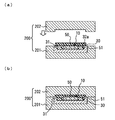
図1は、本実施形態に係る熱式流量センサの概略構成を示す図であり、(a)は上面視平面図、(b)は(a)のA−A断面における断面図、(c)は(a)のB−B断面における断面図である。
Hereinafter, embodiments of the present invention will be described with reference to the drawings. In the following embodiments, a thermal flow sensor will be described as an example of the sensor device.
(First embodiment)
1A and 1B are diagrams showing a schematic configuration of a thermal flow sensor according to the present embodiment, wherein FIG. 1A is a plan view in top view, FIG. 1B is a cross-sectional view taken along the line AA in FIG. FIG. 4 is a cross-sectional view taken along line BB in FIG.
図1(a)〜(c)に示すように、本実施形態における熱式流量センサ100は、一部が被測定流体である空気に露出されて、その流量を検出する流量検出チップ10、流量検出チップ10と電気的に接続され、外部と接続されるリード20、流量検出チップ10を搭載する支持部材30、流量検出チップ10とリード20の接続部を被覆するモールド材40、及び外部からの圧力によって変形する緩衝部材50とにより構成される。尚、図1(a),(b)において、符号60は、流量検出チップ10とリード20を電気的に接続するボンディングワイヤを示している。しかしながら、流量検出チップ10とリード20との接続は上記例に限定されるものではない。それ以外にも、例えばバンプ等によって接続しても良い。
As shown in FIGS. 1A to 1C, a
流量検出チップ10は、例えばシリコンからなる半導体基板11に、エッチングにより空洞部12を形成することにより、空洞部12上に形成された薄い絶縁膜から構成される薄肉部(メンブレン)13と、薄肉部13に形成されたヒータ14とを有している。このように、基板として半導体基板11を用いると、薄肉部13の裏面側からエッチングすることで、簡単に薄肉部13を形成することができ、後述するように、ヒータ14を高感度の流量検出部として機能させることができる。
The flow
ここで、流量検出チップ10について図2を用いてより詳細に説明する。図2は、流量検出チップ10の概略構成を示す上面視平面図である。尚、図2においては、便宜上モールド材40を省略して図示しており、2点鎖線よりも右側(実線矢印方向)がモールド材40により被覆される部分を示している。
Here, the flow
薄肉部13は半導体基板11に比べて非常に薄く形成されているため、薄肉部13の熱容量は低く抑えられ、薄肉部13では半導体基板11との熱的な絶縁が確保される。図2に示すように、薄肉部13には、空気流(白抜き矢印)の上流側と下流側において、発熱抵抗体からなる一対のヒータ14が形成されている。このヒータ14が特許請求の範囲に示した検出素子に相当する。また、ヒータ14を挟むようにして、空気流の上流側と下流側において、測温抵抗体からなる一対の感温部15が、薄肉部13の周りの半導体基板11上に形成されている。
Since the
ヒータ14は、電流の供給量によって発熱する発熱体としての機能に加えて、それ自身の抵抗温度係数の変化に基づいて、自身の温度をも感知する機能を有している。そして、上流側と下流側の各ヒータ14で生じる熱のうち、流通する空気によって奪われる熱に基づき、空気の流量を検出する。さらに、上流側のヒータ14と上流側の感温部15との温度差、及び、下流側のヒータ14と下流側の感温部15との温度差に基づき、各ヒータ14に供給される電流量が制御される。
The
尚、図2において、符号16は配線であり、符号17は配線16の端部に設けられた電極としてのパッドである。そしてパッド17に接続されたボンディングワイヤ60を介して、流量検出部とリード20とが電気的に接続されている。このように、流量検出部は、薄肉部13に形成されたヒータ部14、感温部15、及び配線16により構成される。また、図2に示すように、配線16の一部及びパッド17がモールド材40により被覆されている。尚、本実施形態においては、流量検出チップ10のパッド17とリード20がボンディングワイヤ60を介して直接接続された構成となっている。しかしながら、処理回路を有する回路基板を介して電気的に接続された構成としても良い。
In FIG. 2,
支持体部材30は、流量検出チップ10を搭載するものであり、本実施形態においてはリード20と同一の材料を加工(エッチング等)することにより形成されている。このように、リード20と同一材料にて構成すると、熱式流量センサ100の構成を簡素化することができる。また、支持部材30上に流量検出チップ10を搭載するので、流量検出チップ10の空洞部12が被測定流体である空気に直接晒されることがない。すなわち、空洞部12の下部に支持部材30が配置されない構成と比べて、乱流によるノイズを低減することができる。
The
具体的には、図1(a),(b)に示すように、支持部材30の一端側に、流量検出チップ10の外形に対してクリアランス分大きな溝部31が例えばハーフエッチングすることにより形成されており、この溝部31内に流量検出チップ10が配置(流量検出部形成面の裏面を下にして例えば接着剤により溝部底面に貼着固定)されている。そして、この配置状態で、流量検出チップ10の流量検出部形成面が支持部材30の表面と略同一平面となるように構成されている。従って、流量検出チップ10と支持部材30との段差により発生する乱流の影響を低減している。しかしながら、流量検出チップ10は、流量検出部形成面の裏面を下にして接着剤により溝部底面に貼着固定されるため、高さ方向のばらつきが多少なりとも生じる。従って、流量検出チップ10の流量検出部形成面にバリが生じることも考えられる。
Specifically, as shown in FIGS. 1A and 1B, a
また、支持部材30には、溝部31に流量検出チップ10を配置した状態で、空洞部12と流量検出チップ10上の外部とを連通させる連通部が形成されている。すなわち、流量検出チップ10の空洞部12は支持部材30によって完全に閉塞されておらず、連通部を介して流量検出チップ10上の外部(被測定流体である空気)と通じた状態にある。従って、空洞部12に存在する流体の温度が、熱式流量センサ100の周囲の温度変化に追従して変化することができるので、空洞部12が支持部材30により密閉された構造よりも、温度変化による測定誤差を低減することができる。
In addition, the
具体的には、図1(a),(b)に示すように、溝部31は、流量検出チップ10に対して所定のクリアランスをもって形成されており、溝部31内に流量検出チップ10を位置決め配置した状態で、溝部31の側面と対向する流量検出チップ10の側面との間には、所定の隙間32が存在する。すなわち、流量検出チップ10の側面にバリが生じることも考えられる。尚、溝部31を構成する支持部材30の部位が、特許請求の範囲に示した位置決め部に相当する。
Specifically, as shown in FIGS. 1A and 1B, the
本実施形態においては、空洞部12の下部にハーフエッチングにより、隙間32に連通する連通溝部33が形成されており、この連通溝部33と隙間32とにより連通部を構成している。このように、連通部を連通溝部33と隙間32により構成すると、連通部の構成を簡素化することができる。また、隙間32を介して流量検出チップ10上の外部から空洞部12に被測定流体である空気が侵入可能な構成であるので、空洞部12に大量の空気が侵入することはなく、乱流によるノイズを低減することができる。
In the present embodiment, a
尚、連通部は、空洞部12に対して1箇所のみ設けられても良いし、複数箇所設けられても良い。空洞部12における乱流の発生しやすさと周囲の温度変化に対する追従性を考慮して、形状や大きさ等とともに決定すれば良い。本実施形態においては、空気の流通方向に沿って連通溝部33が形成されており、流量検出チップ10を挟んで、対向位置に連通部が1箇所ずつ形成されている。
Note that the communication portion may be provided only at one location with respect to the
ここで、本実施形態においては、隙間32のうち、モールド材40によって被覆される領域との境界から薄肉部13及びヒータ14の形成位置に対応する位置までの領域の一部を、他の領域よりも広い広域隙間32aとしている。そして、この広域隙間32aに、緩衝部材50を配置している。このように、緩衝部材50の配置領域に対応する隙間32を、他の領域よりも広い広域隙間32aとすると、緩衝部材50を位置決め配置しやすい。また、支持部材30との接触面積が増加するので、緩衝部材50を支持部材30に固定する場合には、より強固に固定することができる。尚、広域隙間32aを設けず、他の領域と同じ幅の隙間32に対して緩衝部材50を配置する構成としても良い。
Here, in the present embodiment, a part of the region from the boundary between the
モールド材40は、エポキシ樹脂等の一体成形可能である電気絶縁材料からなり、支持部材30の溝部31に流量検出チップ10が配置され、空洞部12が流量検出チップ10上の外部と連通部を介して連通し、流量検出チップ10と溝部31との隙間32の広域隙間32a部位に緩衝部材50が配置された状態で、ボンディングワイヤ60、及び各ボンディングワイヤ60との接続部位(流量検出チップ10及びリード20)を、一体的に被覆している。
The
緩衝部材50は、外部(例えば型)からの圧力を受けて変形することで、バリが生じる原因となる隙間(例えば型と流量検出チップ10との間の隙間や、流量検出チップ10と支持部材30との間の隙間等)を埋めることができるものであれば適用が可能である。例えば、型からの圧力を受けて弾性変形するとともに、モールド材40の射出圧に対する耐性を有するものを適用することが好ましい。このような材料から構成されるものであれば、モールド材40を確実にシールドすることができる。本実施形態においては、酸等が存在する環境に配置されることを考慮して、耐薬性に優れるフッ素系のゴムを適用している。
The
また、緩衝部材50は、バリが生じる原因となる隙間を埋めるべく、流量検出チップ10のモールド材40によって被覆される領域との境界から薄肉部13及びヒータ14の形成位置までの領域上の少なくとも一部に配置されれば良い。本実施形態においては、上記したように、流量検出チップ10の流量検出部形成面及び側面(隙間32)にバリを生じる恐れがある。すなわち、流量検出チップ10の流量検出部形成面及び両側面に配置する必要がある。
Further, the
そこで、本実施形態においては、緩衝部材50を、図1(a)〜(c)に示すように略コの字状としている。また、緩衝部材50によって乱流を生じることのないように、薄肉部13の端部(モールド材40側)から3mm以上の距離を確保しつつ、モールド材40との境界位置から流量検出部方向に所定範囲まで緩衝部材50及びそれに対応する広域隙間32aを設けている。また、支持部材30に接する両端部を支持部材30に接着固定している。
Therefore, in the present embodiment, the
次に、このように構成される熱式流量センサ100の製造方法について、図3(a)〜(c)及び図4(a),(b)を用いて説明する。図3は、熱式流量センサ100の製造方法を示す工程別断面図であり、(a)は搭載工程、(b)は接続工程、(c)はモールド工程を示す図である。図3(a)〜(c)は図1(b)に対応している。図4は、緩衝部材50の効果を説明するための図であり、(a)は型締め前、(b)は型締め時の状態を示している。図4(a),(b)は図1(c)に対応している。
Next, a manufacturing method of the
流量検出チップ10及び支持部材30が準備された状態で、先ず、図3(a)に示すように、支持部材30の溝部31に対して流量検出チップ10を位置決めし、例えば貼着固定する。このとき、流量検出チップ10の流量検出部形成面と支持部材30の表面が略同一平面となり、流量検出チップ10と溝部31の側面との間に所定の隙間32(広域隙間32aを含む)が形成される。以上が搭載工程である。
In a state where the flow
次に、図3(b)に示すように、流量検出チップ10のパッド17(図2参照)とリード20とをボンディングワイヤ60により電気的に接続する。以上が接続工程である。
Next, as shown in FIG. 3B, the pads 17 (see FIG. 2) of the flow
そして、図3(c)に示すように、流量検出チップ10に対して、緩衝部材50をモールド材40により被覆される領域との境界から薄肉部13及びヒータ14までの領域の所定位置に配置した状態で、ボンディングワイヤ60、及びボンディングワイヤ60との接続部位(流量検出チップ10及びリード20)がモールド材40によって一体的に被覆されるように、所定の型を用いて一体成形する。
Then, as shown in FIG. 3C, the
より具体的には、支持部材30上に流量検出チップ10が搭載され、リード20が流量検出チップ10に接続された状態において、略コの字状の緩衝部材50の両端を、それぞれ支持部材30に接着固定する。そして、緩衝部材50の配置状態において、金型200を構成する下型201に流量検出チップ10の搭載面の裏面を下にして上記構造体を配置する。この状態が図4(a)に示す型締め前の状態である。この型締め前の状態において、緩衝部材50には外力が印加されておらず、広域隙間32aの少なくとも一部が閉塞されてない状態にある。
More specifically, in a state where the flow
そして、下型201と対をなす上型202を下降させ、型締めする。この型締め状態において、緩衝部材50は上型202からの圧力によって、上型202、下型201、流量検出チップ10、及び支持部材30の間で変形し、図4(b)に示すように、これらの間に形成されるバリを生じる原因となる隙間を埋める。従って、下型201及び上型202にて構成されるキャビティ内に、図示されないゲートを介してモールド材40が射出された際に、緩衝部材40にてモールド材40をシールドし、緩衝部材40よりも流量検出部側へのモールド材40の漏れを防ぐことができる。
Then, the
尚、本実施形態においては、リード20及び支持部材30が同一の構成材料からなり、上記工程において、図示されない外周フレームによって一体化されている。このようにリード20と支持部材30とを一体化した構成とすると、流量検出チップ10を含めて、お互いの位置精度を向上することができる。また、接続工程及びモールド工程を簡素化することができる。そして、モールド材40の射出後のキュアを経て(モールド工程終了後)、外周フレーム部分を切除する分離工程を実施する。そして、熱式流量センサ100が形成される。
In the present embodiment, the
このように本実施形態に係る熱式流量センサ100及びその製造方法によると、流量検出チップ10のモールド材40によって被覆される領域との境界から薄肉部13及びヒータ14までの領域上の少なくとも一部に、緩衝部材50を配置した状態で型締めし、モールド材40を射出する。従って、型締め時に、緩衝部材50が上型202からの圧力を受けて変形し、例えば流量検出チップ10と上型202との間の隙間、流量検出チップ10と支持部材30との間の隙間といった、バリが生じる恐れがある隙間を確実に埋める(閉塞する)ことができる。すなわち、バリが生じるのを防ぐことができるので、検出精度を向上することができる。
As described above, according to the
特に、熱式流量センサ100においては、ヒータ形成面にバリが生じると、検出感度が低下することとなる。また、ヒータ形成面及び側面にバリが生じると、バリによって乱流が発生し、乱流起因のノイズが大きくなる。従って、緩衝部材50を配置する構成が効果的である。
In particular, in the
尚、本実施形態においては、モールド工程において、緩衝部材50を流量検出チップ10及び支持部材30に対して配置する例を示したが、モールド工程以前(例えば搭載工程や接続工程)に配置しても良い。
In the present embodiment, an example in which the
また、本実施形態においては、緩衝部材50を熱式流量センサ100の構成要素の一部としている。検出環境に晒される流量検出部とモールド材40との間に、緩衝部材50を配置しているので、配線16(パッド17)とリード20との接続部の腐食防止効果を高めることができる。しかしながら、熱式流量センサ100として、緩衝部材50を有さない構成としても良い。例えば、緩衝部材50を流量検出チップ10及び支持部材30に固定せずに、広域隙間32aに配置し、モールド工程実施後、緩衝部材50を取り外しても良い。このような製造方法であっても、バリが生じるのを防ぐことができ、検出精度を向上することができる。また、緩衝部材50を繰り返し使用することが可能であるので、コストを低減することができる。
In the present embodiment, the
また、本実施形態においては、空洞部12に存在する流体の温度が、熱式流量センサ100の周囲の温度変化に追従して変化することができるように、空洞部12の下部にハーフエッチングにより、隙間32に連通する連通溝部33を形成し、この連通溝部33と隙間32とにより連通部を構成する例を示した。しかしながら、流量検出チップ10と支持部材30の構成が上記例に限定されるものではない。連通部を有さない構成としても良い。
In the present embodiment, the temperature of the fluid existing in the
また、本実施形態においては、緩衝部材50が1つの部材から構成される例を示した。しかしながら、図5(a)に示すように複数の部材(図中においては2つ)から構成されても良い。複数の部材であっても、図5(b)に示すように、型締め時にバリが生じる隙間を完全に閉塞できれば良い。尚、図5は緩衝部材50の変形例を示す概略断面図であり、(a)は型締め前、(b)は型締め時である。しかしながら、本実施形態に示したように、緩衝部材50を1つの部材で構成すると簡素であり、位置決めしやすい。
Moreover, in this embodiment, the
(第2の実施形態)
次に、本発明の第2の実施形態を、図6及び図7(a),(b)に基づいて説明する。図6は、本実施形態における熱式流量センサ100の概略構成を示す断面図であり、図1(c)に対応している。図7は、モールド工程を説明するための概略断面図であり、(a)は型締め前、(b)は型締め時である。図7(a),(b)は図4(a),(b)に対応している。
(Second Embodiment)
Next, a second embodiment of the present invention will be described with reference to FIGS. 6 and 7A and 7B. FIG. 6 is a cross-sectional view showing a schematic configuration of the
第2の実施形態における熱式流量センサ100及びその製造方法は、第1の実施形態によるものと共通するところが多いので、以下、共通部分については詳しい説明は省略し、異なる部分を重点的に説明する。
Since the
第2の実施形態において、第1の実施形態と異なる点は、緩衝部材50とともに封止材51を用いて、バリを生じる隙間を埋める点である。後の構成は第1の実施形態と同様である。
In the second embodiment, the difference from the first embodiment is that a sealing
第1の実施形態に示したように、緩衝部材50のみによってバリが生じる隙間を全て埋めても良いが、隙間の一部を他の部材によって埋めて、残りを緩衝部材によって埋める構成としても良い。図6に示すように、本実施形態に係る熱式流量センサ100は、流量検出チップ10の側面と支持部材30との間の隙間32(広域隙間32a)に、所定深さまで封止材51が配置され、封止材51及び流量検出チップ10上に緩衝部材50が配置されている。
As shown in the first embodiment, all gaps where burrs are generated may be filled only by the
封止材51としては、隙間32(広域隙間32a)に注入でき、注入後硬化して、モールド材40の射出時に隙間32へのモールド材40の侵入を抑制することのできる材料であれば適用することができる。本実施形態においては、エポキシ系接着剤を適用している。接着剤を適用すると、モールド材40の侵入を防止するだけでなく、支持部材30に対して流量検出チップ10をより強固に固定することができる。
As the sealing
尚、本実施形態における緩衝部材50は、流量検出チップ10のヒータ形成面に接着固定されており、溝部31よりも外周側の支持部材30の領域上まで設けられている。
In addition, the
このように、緩衝部材50だけでなく、封止材51によって隙間を埋める構成の場合、モールド工程において、先ず、図7(a)に示すように、流量検出チップ10の側面と支持部材30との間の隙間32の少なくとも一部(広域隙間32a)に液状の封止材51を充填し、封止材51を硬化させる。そして、封止材51の硬化後、緩衝部材50を封止材51及び流量検出チップ10上に配置する。
Thus, in the case of a configuration in which not only the
次いで、緩衝部材50の配置後、図7(b)に示すように、上型202を下降させて下型201とにより型締めする。このとき、緩衝部材50が上型202からの圧力を受けて変形し、封止材51によって埋められた隙間を除くバリが生じる隙間を埋める。そして、モールド材40が金型200のキャビティ内に射出される。
Next, after the
このように本実施形態に係る熱式流量センサ100及びその製造方法によっても、バリが生じるのを防ぐことができるので、検出精度を向上することができる。また、流量検出チップ10と支持部材30との間の隙間32に緩衝部材50の配置が困難である場合に、液状の封止材51を充填し、その後硬化させて埋める本実施形態の方法が特に効果的である。
As described above, the
尚、本実施形態においては、モールド工程において、封止部材51を広域隙間32aに配置する例を示したが、モールド工程以前に配置しても良い。また、緩衝部材50も、封止材51を硬化した後であれば、モールド工程以前に配置しても良い。
In the present embodiment, the example in which the sealing
また、本実施形態においても、緩衝部材50を熱式流量センサ100の構成要素の一部としている。しかしながら、熱式流量センサ100として、緩衝部材50を有さない構成としても良い。例えば、緩衝部材50を流量検出チップ10に固定せずに封止材51及び流量検出チップ10上に配置し、モールド工程実施後、緩衝部材50を取り外しても良い。このような製造方法であっても、バリが生じるのを防ぐことができ、検出精度を向上することができる。また、緩衝部材50を繰り返し使用することが可能であるので、コストを低減することができる。
Also in this embodiment, the
(第3の実施形態)
次に、本発明の第3の実施形態を、図8及び図9(a),(b)に基づいて説明する。図8は、本実施形態における熱式流量センサ100の概略構成を示す断面図であり、図1(c)に対応している。図9は、モールド工程を説明するための概略断面図であり、(a)は型締め前、(b)は型締め時である。図6(a),(b)は図4(a),(b)に対応している。
(Third embodiment)
Next, a third embodiment of the present invention will be described with reference to FIGS. 8 and 9A and 9B. FIG. 8 is a cross-sectional view showing a schematic configuration of the
第3の実施形態における熱式流量センサ100及びその製造方法は、第1及び第2の実施形態によるものと共通するところが多いので、以下、共通部分については詳しい説明は省略し、異なる部分を重点的に説明する。
Since the
第3の実施形態において、第1及び第2の実施形態と異なる点は、支持部材30の形状である点である。
The third embodiment is different from the first and second embodiments in the shape of the
図8に示すように、本実施形態に係る熱式流量センサ100は、支持部材30に溝部31が設けられていない。あとの構成は第1の実施形態と同様である。また第2の実施形態を適用することもできる。
As shown in FIG. 8, the
このような構成においても、支持部材30上への流量センサチップ10の搭載位置のばらつき及び、搭載高さのばらつきを考慮して、上型202と流量センサチップとの間には所定のクリアランスが設けてある。すなわち、金型200と流量センサチップ10との間には所定の隙間が存在する。従って、図9(a)に示すように、緩衝部材50を配置した状態で型締めを行えば、図9(b)に示すように、緩衝部材50が上型202からの圧力を受けて変形し、バリが生じる上記隙間を埋めることができる。
Even in such a configuration, a predetermined clearance is provided between the
尚、緩衝部材50は流量センサチップ10及び支持部材30の少なくとも一方に固定されても良いし、固定されずにモールド工程終了後、取り除かれても良い。図8に示す熱式流量センサ100においては、支持部材30に接着固定されている。
The
(第3の実施形態)
次に、本発明の第3の実施形態を、図8及び図9(a),(b)に基づいて説明する。図8は、本実施形態における熱式流量センサ100の概略構成を示す断面図であり、図1(c)に対応している。図9は、モールド工程を説明するための概略断面図であり、(a)は型締め前、(b)は型締め時である。図9(a),(b)は図4(a),(b)に対応している。
(Third embodiment)
Next, a third embodiment of the present invention will be described with reference to FIGS. 8 and 9A and 9B. FIG. 8 is a cross-sectional view showing a schematic configuration of the
第3の実施形態における熱式流量センサ100及びその製造方法は、第1及び第2の実施形態によるものと共通するところが多いので、以下、共通部分については詳しい説明は省略し、異なる部分を重点的に説明する。
Since the
第3の実施形態において、第1及び第2の実施形態と異なる点は、支持部材30の形状である点である。
The third embodiment is different from the first and second embodiments in the shape of the
図8に示すように、本実施形態に係る熱式流量センサ100は、支持部材30に溝部31が設けられていない。あとの構成は第1の実施形態と同様である。また第2の実施形態を適用することもできる。
As shown in FIG. 8, the
このような構成においても、支持部材30上への流量センサチップ10の搭載位置のばらつき及び、搭載高さのばらつきを考慮して、上型202と流量センサチップとの間には所定のクリアランスが設けてある。すなわち、金型200と流量センサチップ10との間には所定の隙間が存在する。従って、図9(a)に示すように、緩衝部材50を配置した状態で型締めを行えば、図9(b)に示すように、緩衝部材50が上型202からの圧力を受けて変形し、バリが生じる上記隙間を埋めることができる。
Even in such a configuration, a predetermined clearance is provided between the
尚、緩衝部材50は流量センサチップ10及び支持部材30の少なくとも一方に固定されても良いし、固定されずにモールド工程終了後、取り除かれても良い。図8に示す熱式流量センサ100においては、支持部材30に接着固定されている。
The
(第4の実施形態)
次に、本発明の第4の実施形態を、図10(a),(b)及び図11(a),(b)に基づいて説明する。図10は、本実施形態における熱式流量センサ100の概略構成を示す断面図であり、(a)は図1(b)に対応し、(b)は図1(c)に対応している。図10は、モールド工程を説明するための概略断面図であり、(a)は型締め前、(b)は型締め時である。図11(a),(b)は図4(a),(b)に対応している。
(Fourth embodiment)
Next, a fourth embodiment of the present invention will be described based on FIGS. 10 (a) and 10 (b) and FIGS. 11 (a) and 11 (b). FIG. 10 is a cross-sectional view illustrating a schematic configuration of the
第4の実施形態における熱式流量センサ100及びその製造方法は、第1〜第3の実施形態によるものと共通するところが多いので、以下、共通部分については詳しい説明は省略し、異なる部分を重点的に説明する。
Since the
第4の実施形態において、第1〜第3の実施形態と異なる点は、支持部材30を有さない点である。
The fourth embodiment is different from the first to third embodiments in that the
図10(a),(b)に示すように、本実施形態に係る熱式流量センサ100は、流量検出チップ10を支持部材30に固定せずにリード20と接続した構成となっている。あとの構成は第1の実施形態と同様である。また第2の実施形態を適用することもできる。
As shown in FIGS. 10A and 10B, the
このような構成においても、流量センサチップ10と金型200との間には所定のクリアランスが設けてある。すなわち、流量センサチップ10と金型200との間には所定の隙間が存在する。従って、図11(a)に示すように、緩衝部材50を配置した状態で型締めを行えば、図11(b)に示すように、緩衝部材50が上型202からの圧力を受けて変形し、バリが生じる上記隙間を埋めることができる。
Even in such a configuration, a predetermined clearance is provided between the flow
尚、緩衝部材50は流量センサチップ10に固定されても良いし、固定されずにモールド工程終了後、取り除かれても良い。図10(a),(b)に示す熱式流量センサ100においては、緩衝部材50は挿通孔を有するリング状に設けられ、流量検出チップ10を挿通しつつ圧入固定されている。
The
以上本発明の好ましい実施形態について説明したが、本発明は上述の実施形態のみに限定されず、種々変更して実施することができる。 Although the preferred embodiments of the present invention have been described above, the present invention is not limited to the above-described embodiments, and can be implemented with various modifications.
本実施形態において、流量検出チップ10を構成する基板はシリコンからなる半導体基板11である例を示した。このように半導体基板11を用いると、一般的な半導体製造技術により、基板に容易に空洞部12及び薄肉部13を形成することができる。すなわち、熱式流量センサ100を低コストで製造することができる。しかしながら、基板はガラス基板等により構成されても良い。
In the present embodiment, an example is shown in which the substrate constituting the flow
また、第1〜第3の実施形態においては、緩衝部材50が流量検出チップ10及び支持部材30の少なくとも一方に接着固定される例を示した。また第4の実施形態においては、圧入固定される例を示した。しかしながら、緩衝部材50の固定方法としては、特に限定されるものではない。例えば、流量検出チップ10及び/又は支持部材30の緩衝部材50との当接位置に、凸部及び凹部の少なくとも一方を設けた構成としても良い。この場合、凸部及び凹部の少なくとも一方に、例えば上型202からの圧力を受けて変形した緩衝部材50を食い込ませて固定することができる。尚、図12に示す熱式流量センサ100においては、支持部材30の溝部31を構成する側面に凸部31aを設け、緩衝部材50を凸部31aに噛み混ませている。図12は、熱式流量センサ100の変形例を示す概略断面図であり、図1(c)に対応している。
In the first to third embodiments, the example in which the
また、本実施形態においては、熱式流量センサ100において、装置100及び製造方法を説明した。しかしながら、本発明(製造方法及び装置)の適用範囲は熱式流量センサ100に限定されるものではない。検出素子を露出させつつ配線部とリードとの接続部位をモールド材にて被覆する構成のセンサ装置であれば適用することができる。上記熱式流量センサ100以外にも、特に基板の薄肉部に、検出素子の少なくとも一部を形成してなるセンサ(例えばサーモパイル式の赤外線センサ、湿度センサ、圧力センサ等)に好適である。
In the present embodiment, the
10・・・流量検出チップ(センサチップ)
11・・・半導体基板(基板)
12・・・空洞部
13・・・薄肉部
14・・・ヒータ(検出素子)
16・・・配線
20・・・リード
30・・・支持部材
31・・・溝部
32・・・隙間
33・・・連通溝部
40・・・モールド材
50・・・緩衝部材
51・・・封止材
60・・・ボンディングワイヤ
100・・・熱式流量センサ(センサ装置)
200・・・金型
10. Flow rate detection chip (sensor chip)
11 ... Semiconductor substrate (substrate)
12 ...
16 ... wiring 20 ... lead 30 ...
200 ... mold
Claims (21)
前記センサチップの配線部とリードを接続する接続工程と、
型内にモールド材を射出して、前記検出素子を露出させつつ前記配線部と前記リードとの接続部位を前記モールド材にて被覆するモールド工程と、を備えるセンサ装置の製造方法であって、
前記接続工程の前に、前記センサチップを検出素子形成面の裏面を搭載面として支持部材上に固定する搭載工程を備え、
前記モールド工程において、前記センサチップの前記モールド材によって被覆される領域との境界から前記検出素子までの領域上の少なくとも一部に、前記型からの圧力を受けて変形する緩衝部材を配置した状態で、型締めして前記モールド材を射出し、
前記緩衝部材は、前記センサチップの検出素子形成面及び両側面に当接する略コの字形状を有していることを特徴とするセンサ装置の製造方法。 A chip forming step of preparing a sensor chip formed on a substrate by forming a detection element and a wiring portion connected to the detection element;
A connecting step of connecting the wiring portion and the lead of the sensor chip;
A molding step of injecting a molding material into a mold and covering the connecting portion of the wiring part and the lead with the molding material while exposing the detection element,
Before the connecting step, the mounting step of fixing the sensor chip on the support member with the back surface of the detection element forming surface as the mounting surface ,
In the molding step, a buffer member that is deformed by receiving pressure from the mold is disposed on at least a part of the region from the boundary of the sensor chip to the region covered with the molding material to the detection element. Then, mold clamping and injecting the mold material ,
The method for manufacturing a sensor device according to claim 1, wherein the buffer member has a substantially U-shape that contacts the detection element forming surface and both side surfaces of the sensor chip .
前記検出素子形成面とともに、前記支持部材を底面とし、前記センサチップの側面と対向する前記位置決め部との間の隙間の少なくとも一部に、前記緩衝部材を配置することを特徴とする請求項1又は請求項2に記載のセンサ装置の製造方法。 The support member has both side surfaces connected to the detection element formation surface of the sensor chip, and positioning portions facing the both side surfaces and the tip surface connected to the detection element formation surface,
Together with the detection element formation surface, the supporting member and the bottom surface, according to claim 1, at least a portion of the gap between the positioning portion facing the side surface of the sensor chip, characterized by arranging the cushioning member Or the manufacturing method of the sensor apparatus of Claim 2 .
前記センサチップの配線部とリードを接続する接続工程と、
型内にモールド材を射出して、前記検出素子を露出させつつ前記配線部と前記リードとの接続部位を前記モールド材にて被覆するモールド工程と、を備えるセンサ装置の製造方法であって、
前記接続工程の前に、前記センサチップを検出素子形成面の裏面を搭載面として支持部材上に固定する搭載工程を備え、
前記支持部材は、前記センサチップの検出素子形成面に連結する両側面と、当該両側面及び前記検出素子形成面に連結する先端面に対して、それぞれ対向する位置決め部を有し、
前記モールド工程において、前記支持部材を底面とし、前記センサチップの側面と対向する前記位置決め部との間の隙間の少なくとも一部に液状の封止材を充填し、前記封止材を硬化後、前記センサチップの前記モールド材によって被覆される領域との境界から前記検出素子までの領域上の少なくとも一部であって前記検出素子形成面上及び前記隙間における前記封止材上に、前記型からの圧力を受けて変形する緩衝部材を配置した状態で、型締めして前記モールド材を射出することを特徴とするセンサ装置の製造方法。 A chip forming step of preparing a sensor chip formed on a substrate by forming a detection element and a wiring portion connected to the detection element;
A connecting step of connecting the wiring portion and the lead of the sensor chip;
A molding step of injecting a molding material into a mold and covering the connecting portion of the wiring part and the lead with the molding material while exposing the detection element,
Before the connecting step, the mounting step of fixing the sensor chip on the support member with the back surface of the detection element forming surface as the mounting surface,
The support member has both side surfaces connected to the detection element formation surface of the sensor chip, and positioning portions facing the both side surfaces and the tip surface connected to the detection element formation surface,
In the molding step, the support member is a bottom surface, and a liquid sealing material is filled in at least a part of a gap between the positioning portion facing the side surface of the sensor chip, and after the sealing material is cured, From the mold, on at least part of the region from the boundary of the sensor chip to the region covered with the mold material to the detection element, on the detection element formation surface and on the sealing material in the gap A manufacturing method of a sensor device, wherein a mold member is clamped and the molding material is injected in a state in which a buffer member that is deformed by receiving pressure is disposed.
前記モールド工程において、前記検出素子及び前記薄肉部を露出させつつ前記配線部と前記リードとの接続部位を前記モールド材にて被覆することを特徴とする請求項1〜7いずれか1項に記載のセンサ装置の製造方法。 The sensor chip has a thin portion formed on the substrate, and at least a part of the detection element is formed on the thin portion,
In the molding step, according to claims 1 to 7 any one, characterized in that for covering the connection portion between the sensing element and the lead and the wiring portion while exposing the thin portion in the molding material Manufacturing method of the sensor device.
前記センサチップを搭載する支持部材と、
前記配線部と電気的に接続されるリードとを備え、
検出素子形成面の裏面を搭載面として前記センサチップを前記支持部材上に搭載した状態で、前記検出素子を露出させつつ前記配線部と前記リードとの接続部位を前記モールド材にて被覆してなるセンサ装置であって、
前記センサチップの検出素子形成面及び当該検出素子形成面に連結する両側面において、前記モールド材にて被覆される領域との境界から前記検出素子までの領域上の少なくとも一部に、外部からの圧力を受けて変形する略コの字形状の緩衝部材を配置したことを特徴とするセンサ装置。 On the substrate, a sensor chip formed by forming a detection element and a wiring portion connected to the detection element;
A support member on which the sensor chip is mounted;
A lead electrically connected to the wiring portion;
With the sensor chip mounted on the support member with the back surface of the detection element formation surface as the mounting surface, the connection portion between the wiring portion and the lead is covered with the mold material while exposing the detection element. A sensor device comprising:
On at least a part of the region from the boundary to the region covered with the molding material to the detection element on the detection element formation surface of the sensor chip and both side surfaces connected to the detection element formation surface, A sensor device comprising a substantially U-shaped buffer member that deforms under pressure.
前記センサチップの側面と対向する前記支持部材の位置決め部との間の隙間に、前記緩衝部材の一部を配置したことを特徴とする請求項10に記載のセンサ装置。 The support member has a positioning portion facing both side surfaces of the sensor chip and a front end surface connected to the both side surfaces and the detection element forming surface, respectively.
The sensor device according to claim 10 , wherein a part of the buffer member is arranged in a gap between a side surface of the sensor chip and a positioning portion of the support member facing the side surface of the sensor chip.
前記センサチップを搭載する支持部材と、
前記配線部と電気的に接続されるリードとを備え、
前記支持部材上に検出素子形成面の裏面を搭載面として前記センサチップを搭載した状態で、前記検出素子を露出させつつ前記配線部と前記リードとの接続部位を前記モールド材にて被覆してなるセンサ装置であって、
前記支持部材は、前記センサチップの両側面と、当該両側面及び前記検出素子形成面に連結する先端面に対して、それぞれ対向する位置決め部を有し、
前記センサチップの側面と対向する前記位置決め部との隙間の、前記モールド材にて被覆される領域との境界から前記検出素子の形成位置に対応する位置までの領域上の少なくとも一部に、前記支持部材を底面として所定深さまで封止材を配置し、前記封止材及び前記検出素子形成面の前記モールド材にて被覆される領域との境界から前記検出素子までの領域の少なくとも一部に、外部からの圧力を受けて変形する緩衝部材を配置したことを特徴とするセンサ装置。 On the substrate, a sensor chip formed by forming a detection element and a wiring portion connected to the detection element;
A support member on which the sensor chip is mounted;
A lead electrically connected to the wiring portion;
With the sensor chip mounted on the support member with the back surface of the detection element formation surface as the mounting surface, the connection portion between the wiring portion and the lead is covered with the mold material while exposing the detection element. A sensor device comprising:
The support member includes positioning portions that face both side surfaces of the sensor chip and front end surfaces connected to the both side surfaces and the detection element forming surface, respectively.
At least part of the gap between the side surface of the sensor chip and the positioning portion facing the side surface of the sensor chip from the boundary with the region covered with the molding material to the position corresponding to the formation position of the detection element, A sealing material is arranged to a predetermined depth with the support member as a bottom surface, and at least a part of the region from the boundary between the sealing material and the region covered with the mold material on the detection element forming surface to the detection element A sensor device in which a buffer member that deforms in response to pressure from the outside is disposed.
前記検出素子及び前記薄肉部を露出させつつ前記配線部と前記リードとの接続部位を前記モールド材にて被覆したことを特徴とする請求項10〜19いずれか1項に記載のセンサ装置。 The sensor chip has a thin portion formed on the substrate, and at least a part of the detection element is formed on the thin portion,
The sensor device according to any one of claims 10 to 19 , wherein a connection portion between the wiring portion and the lead is covered with the molding material while exposing the detection element and the thin portion.
Priority Applications (3)
| Application Number | Priority Date | Filing Date | Title |
|---|---|---|---|
| JP2005221512A JP4830391B2 (en) | 2005-07-29 | 2005-07-29 | Manufacturing method of sensor device and sensor device |
| US11/485,318 US7404321B2 (en) | 2005-07-29 | 2006-07-13 | Sensor device having a buffer element between the molding and the sensing element |
| DE102006035000A DE102006035000B4 (en) | 2005-07-29 | 2006-07-28 | Sensor device and method for its production |
Applications Claiming Priority (1)
| Application Number | Priority Date | Filing Date | Title |
|---|---|---|---|
| JP2005221512A JP4830391B2 (en) | 2005-07-29 | 2005-07-29 | Manufacturing method of sensor device and sensor device |
Publications (2)
| Publication Number | Publication Date |
|---|---|
| JP2007033411A JP2007033411A (en) | 2007-02-08 |
| JP4830391B2 true JP4830391B2 (en) | 2011-12-07 |
Family
ID=37670198
Family Applications (1)
| Application Number | Title | Priority Date | Filing Date |
|---|---|---|---|
| JP2005221512A Expired - Fee Related JP4830391B2 (en) | 2005-07-29 | 2005-07-29 | Manufacturing method of sensor device and sensor device |
Country Status (3)
| Country | Link |
|---|---|
| US (1) | US7404321B2 (en) |
| JP (1) | JP4830391B2 (en) |
| DE (1) | DE102006035000B4 (en) |
Families Citing this family (24)
| Publication number | Priority date | Publication date | Assignee | Title |
|---|---|---|---|---|
| JP4685663B2 (en) * | 2006-03-03 | 2011-05-18 | 日本電信電話株式会社 | Self-driven telemetry observation device |
| EP2251651A3 (en) * | 2007-04-26 | 2012-02-22 | Heraeus Sensor Technology Gmbh | Mounting arrangement of a metal film resistor of an anemometric measuring device within an exhaust gas conduit |
| DE102007024865A1 (en) * | 2007-05-29 | 2008-12-04 | Robert Bosch Gmbh | Device for determining at least one parameter of a fluid medium |
| US8028584B2 (en) * | 2007-08-20 | 2011-10-04 | Denso Corporation | Pressure sensor and method for manufacturing the same |
| US8438931B2 (en) * | 2007-08-27 | 2013-05-14 | Hitachi, Ltd. | Semiconductor strain sensor |
| JP4577370B2 (en) * | 2008-02-12 | 2010-11-10 | 株式会社デンソー | Sensor device and manufacturing method thereof |
| DE102008037206B4 (en) * | 2008-08-11 | 2014-07-03 | Heraeus Sensor Technology Gmbh | 300 ° C-Flow Sensor |
| JP4978587B2 (en) | 2008-08-21 | 2012-07-18 | 株式会社デンソー | Sensor device and manufacturing method thereof |
| EP2224218B1 (en) * | 2009-02-25 | 2018-11-28 | Sensirion Automotive Solutions AG | A sensor in a moulded package and a method for manufacturing the same |
| JP5318737B2 (en) * | 2009-12-04 | 2013-10-16 | 株式会社デンソー | Sensor device and manufacturing method thereof |
| JP5208099B2 (en) | 2009-12-11 | 2013-06-12 | 日立オートモティブシステムズ株式会社 | Flow sensor, method for manufacturing the same, and flow sensor module |
| US8425217B2 (en) * | 2009-12-23 | 2013-04-23 | Rodney J. Groleau | Method for installing indirect and direct mold pressure, temperature and flow front detection sensors without machining the mold |
| JP5541208B2 (en) * | 2011-03-24 | 2014-07-09 | 株式会社デンソー | Mechanical quantity sensor |
| JP5333529B2 (en) | 2011-07-05 | 2013-11-06 | 株式会社デンソー | Mold package manufacturing method |
| DE102012009421A1 (en) * | 2012-05-11 | 2013-11-14 | E + E Elektronik Ges.M.B.H. | flow sensor |
| JP5632881B2 (en) | 2012-06-15 | 2014-11-26 | 日立オートモティブシステムズ株式会社 | Thermal flow meter |
| JP5648021B2 (en) * | 2012-06-29 | 2015-01-07 | 日立オートモティブシステムズ株式会社 | Thermal air flow sensor |
| US9448130B2 (en) * | 2013-08-31 | 2016-09-20 | Infineon Technologies Ag | Sensor arrangement |
| JP6101619B2 (en) * | 2013-11-12 | 2017-03-22 | 日立オートモティブシステムズ株式会社 | Thermal air flow meter |
| EP3176543B1 (en) | 2014-07-30 | 2020-11-18 | Hitachi Automotive Systems, Ltd. | Circuit board mounting structure and sensor using same |
| JP5976085B2 (en) * | 2014-12-01 | 2016-08-23 | 日立オートモティブシステムズ株式会社 | Flow sensor, method for manufacturing the same, and flow sensor module |
| GB2539944B (en) * | 2015-07-02 | 2018-03-14 | Ing Dah Entpr Co Ltd | Container lid assembly |
| JP6416357B1 (en) * | 2017-10-05 | 2018-10-31 | 三菱電機株式会社 | Flow measuring device |
| CN117030804B (en) * | 2023-10-10 | 2023-12-12 | 冰零智能科技(常州)有限公司 | Sensor and use method thereof |
Family Cites Families (13)
| Publication number | Priority date | Publication date | Assignee | Title |
|---|---|---|---|---|
| JPH02301156A (en) * | 1989-05-15 | 1990-12-13 | Murata Mfg Co Ltd | Electronic device |
| JP2784286B2 (en) * | 1991-12-09 | 1998-08-06 | 三菱電機株式会社 | Method for manufacturing semiconductor sensor device |
| JPH10197374A (en) * | 1997-01-14 | 1998-07-31 | Mitsubishi Electric Corp | Semiconductor sensor |
| JP3328547B2 (en) | 1997-06-16 | 2002-09-24 | 株式会社日立製作所 | Thermal air flow sensor |
| DE19744997A1 (en) * | 1997-10-11 | 1999-04-15 | Bosch Gmbh Robert | Device for measuring the mass of a flowing medium |
| JP3563640B2 (en) | 1999-06-23 | 2004-09-08 | 帝国通信工業株式会社 | Method of insert molding magnetic sensor element into mold resin |
| JP3587734B2 (en) * | 1999-06-30 | 2004-11-10 | 株式会社日立製作所 | Thermal air flow sensor |
| JP2001296197A (en) | 2000-04-12 | 2001-10-26 | Denso Corp | Pressure sensor |
| DE10036290A1 (en) * | 2000-07-26 | 2002-02-07 | Bosch Gmbh Robert | Device for determining at least one parameter of a flowing medium |
| JP2003001674A (en) * | 2001-06-26 | 2003-01-08 | Nec Kansai Ltd | Resin molding apparatus |
| JP2004028631A (en) * | 2002-06-21 | 2004-01-29 | Mitsubishi Electric Corp | Flow sensor |
| JP4281630B2 (en) * | 2004-06-18 | 2009-06-17 | 株式会社デンソー | Manufacturing method of sensor device |
| JP4609019B2 (en) * | 2004-09-24 | 2011-01-12 | 株式会社デンソー | Thermal flow sensor and manufacturing method thereof |
-
2005
- 2005-07-29 JP JP2005221512A patent/JP4830391B2/en not_active Expired - Fee Related
-
2006
- 2006-07-13 US US11/485,318 patent/US7404321B2/en active Active
- 2006-07-28 DE DE102006035000A patent/DE102006035000B4/en not_active Expired - Fee Related
Also Published As
| Publication number | Publication date |
|---|---|
| DE102006035000A1 (en) | 2007-02-08 |
| US20070022808A1 (en) | 2007-02-01 |
| JP2007033411A (en) | 2007-02-08 |
| DE102006035000B4 (en) | 2009-07-16 |
| US7404321B2 (en) | 2008-07-29 |
Similar Documents
| Publication | Publication Date | Title |
|---|---|---|
| JP4830391B2 (en) | Manufacturing method of sensor device and sensor device | |
| KR100720613B1 (en) | Thermal-type flow rate sensor and manufacturing method thereof | |
| JP4249193B2 (en) | Semiconductor pressure sensor device | |
| JP4281630B2 (en) | Manufacturing method of sensor device | |
| CN102575955B (en) | Flow sensor and manufacture method thereof and flow sensor module and manufacture method thereof | |
| EP3660470B1 (en) | Flow sensor and method for manufacturing flow sensor | |
| JP5012330B2 (en) | Manufacturing method of sensor device and sensor device | |
| JP4548066B2 (en) | Pressure sensor | |
| JP2009505088A (en) | Sensor arrangement structure including substrate and casing and method for manufacturing sensor arrangement structure | |
| JP2005274412A (en) | Temperature sensor integrated type pressure sensor device | |
| JP2009031067A (en) | Sensor device | |
| JP4821786B2 (en) | Temperature sensor and temperature sensor integrated pressure sensor | |
| KR101715244B1 (en) | Pressure sensor device and method of fabricating the same | |
| US7737544B2 (en) | Sensor system having a substrate and a housing, and method for manufacturing a sensor system | |
| JP6317956B2 (en) | Pressure sensor and method of manufacturing pressure sensor | |
| JP4717088B2 (en) | Manufacturing method of semiconductor pressure sensor device | |
| JP4963069B2 (en) | Pressure sensor | |
| JP4983329B2 (en) | Sensor device | |
| JP3149678B2 (en) | Semiconductor pressure sensor | |
| JP4830669B2 (en) | Sensor device and manufacturing method thereof | |
| JP2014211389A (en) | Pressure detector | |
| JP2014126515A (en) | Pressure sensor and manufacturing method of the same | |
| JP2002310830A (en) | Manufacturing method of sensor device | |
| JP2018165679A (en) | Physical quantity detection device |
Legal Events
| Date | Code | Title | Description |
|---|---|---|---|
| A621 | Written request for application examination |
Free format text: JAPANESE INTERMEDIATE CODE: A621 Effective date: 20070806 |
|
| A977 | Report on retrieval |
Free format text: JAPANESE INTERMEDIATE CODE: A971007 Effective date: 20100628 |
|
| A131 | Notification of reasons for refusal |
Free format text: JAPANESE INTERMEDIATE CODE: A131 Effective date: 20101207 |
|
| A521 | Request for written amendment filed |
Free format text: JAPANESE INTERMEDIATE CODE: A523 Effective date: 20110113 |
|
| TRDD | Decision of grant or rejection written | ||
| A01 | Written decision to grant a patent or to grant a registration (utility model) |
Free format text: JAPANESE INTERMEDIATE CODE: A01 Effective date: 20110823 |
|
| A01 | Written decision to grant a patent or to grant a registration (utility model) |
Free format text: JAPANESE INTERMEDIATE CODE: A01 |
|
| A61 | First payment of annual fees (during grant procedure) |
Free format text: JAPANESE INTERMEDIATE CODE: A61 Effective date: 20110905 |
|
| R151 | Written notification of patent or utility model registration |
Ref document number: 4830391 Country of ref document: JP Free format text: JAPANESE INTERMEDIATE CODE: R151 |
|
| FPAY | Renewal fee payment (event date is renewal date of database) |
Free format text: PAYMENT UNTIL: 20140930 Year of fee payment: 3 |
|
| R250 | Receipt of annual fees |
Free format text: JAPANESE INTERMEDIATE CODE: R250 |
|
| R250 | Receipt of annual fees |
Free format text: JAPANESE INTERMEDIATE CODE: R250 |
|
| R250 | Receipt of annual fees |
Free format text: JAPANESE INTERMEDIATE CODE: R250 |
|
| R250 | Receipt of annual fees |
Free format text: JAPANESE INTERMEDIATE CODE: R250 |
|
| R250 | Receipt of annual fees |
Free format text: JAPANESE INTERMEDIATE CODE: R250 |
|
| R250 | Receipt of annual fees |
Free format text: JAPANESE INTERMEDIATE CODE: R250 |
|
| R250 | Receipt of annual fees |
Free format text: JAPANESE INTERMEDIATE CODE: R250 |
|
| LAPS | Cancellation because of no payment of annual fees |