JP4736821B2 - Pattern forming method and pattern forming apparatus - Google Patents
Pattern forming method and pattern forming apparatus Download PDFInfo
- Publication number
- JP4736821B2 JP4736821B2 JP2006014525A JP2006014525A JP4736821B2 JP 4736821 B2 JP4736821 B2 JP 4736821B2 JP 2006014525 A JP2006014525 A JP 2006014525A JP 2006014525 A JP2006014525 A JP 2006014525A JP 4736821 B2 JP4736821 B2 JP 4736821B2
- Authority
- JP
- Japan
- Prior art keywords
- mold
- substrate
- pattern
- alignment mark
- light
- Prior art date
- Legal status (The legal status is an assumption and is not a legal conclusion. Google has not performed a legal analysis and makes no representation as to the accuracy of the status listed.)
- Expired - Fee Related
Links
Images


Classifications
-
- G—PHYSICS
- G03—PHOTOGRAPHY; CINEMATOGRAPHY; ANALOGOUS TECHNIQUES USING WAVES OTHER THAN OPTICAL WAVES; ELECTROGRAPHY; HOLOGRAPHY
- G03F—PHOTOMECHANICAL PRODUCTION OF TEXTURED OR PATTERNED SURFACES, e.g. FOR PRINTING, FOR PROCESSING OF SEMICONDUCTOR DEVICES; MATERIALS THEREFOR; ORIGINALS THEREFOR; APPARATUS SPECIALLY ADAPTED THEREFOR
- G03F9/00—Registration or positioning of originals, masks, frames, photographic sheets or textured or patterned surfaces, e.g. automatically
- G03F9/70—Registration or positioning of originals, masks, frames, photographic sheets or textured or patterned surfaces, e.g. automatically for microlithography
- G03F9/7049—Technique, e.g. interferometric
-
- B—PERFORMING OPERATIONS; TRANSPORTING
- B82—NANOTECHNOLOGY
- B82Y—SPECIFIC USES OR APPLICATIONS OF NANOSTRUCTURES; MEASUREMENT OR ANALYSIS OF NANOSTRUCTURES; MANUFACTURE OR TREATMENT OF NANOSTRUCTURES
- B82Y10/00—Nanotechnology for information processing, storage or transmission, e.g. quantum computing or single electron logic
-
- B—PERFORMING OPERATIONS; TRANSPORTING
- B82—NANOTECHNOLOGY
- B82Y—SPECIFIC USES OR APPLICATIONS OF NANOSTRUCTURES; MEASUREMENT OR ANALYSIS OF NANOSTRUCTURES; MANUFACTURE OR TREATMENT OF NANOSTRUCTURES
- B82Y40/00—Manufacture or treatment of nanostructures
-
- G—PHYSICS
- G03—PHOTOGRAPHY; CINEMATOGRAPHY; ANALOGOUS TECHNIQUES USING WAVES OTHER THAN OPTICAL WAVES; ELECTROGRAPHY; HOLOGRAPHY
- G03F—PHOTOMECHANICAL PRODUCTION OF TEXTURED OR PATTERNED SURFACES, e.g. FOR PRINTING, FOR PROCESSING OF SEMICONDUCTOR DEVICES; MATERIALS THEREFOR; ORIGINALS THEREFOR; APPARATUS SPECIALLY ADAPTED THEREFOR
- G03F7/00—Photomechanical, e.g. photolithographic, production of textured or patterned surfaces, e.g. printing surfaces; Materials therefor, e.g. comprising photoresists; Apparatus specially adapted therefor
- G03F7/0002—Lithographic processes using patterning methods other than those involving the exposure to radiation, e.g. by stamping
-
- G—PHYSICS
- G03—PHOTOGRAPHY; CINEMATOGRAPHY; ANALOGOUS TECHNIQUES USING WAVES OTHER THAN OPTICAL WAVES; ELECTROGRAPHY; HOLOGRAPHY
- G03F—PHOTOMECHANICAL PRODUCTION OF TEXTURED OR PATTERNED SURFACES, e.g. FOR PRINTING, FOR PROCESSING OF SEMICONDUCTOR DEVICES; MATERIALS THEREFOR; ORIGINALS THEREFOR; APPARATUS SPECIALLY ADAPTED THEREFOR
- G03F9/00—Registration or positioning of originals, masks, frames, photographic sheets or textured or patterned surfaces, e.g. automatically
- G03F9/70—Registration or positioning of originals, masks, frames, photographic sheets or textured or patterned surfaces, e.g. automatically for microlithography
- G03F9/7003—Alignment type or strategy, e.g. leveling, global alignment
- G03F9/7023—Aligning or positioning in direction perpendicular to substrate surface
- G03F9/703—Gap setting, e.g. in proximity printer
-
- G—PHYSICS
- G03—PHOTOGRAPHY; CINEMATOGRAPHY; ANALOGOUS TECHNIQUES USING WAVES OTHER THAN OPTICAL WAVES; ELECTROGRAPHY; HOLOGRAPHY
- G03F—PHOTOMECHANICAL PRODUCTION OF TEXTURED OR PATTERNED SURFACES, e.g. FOR PRINTING, FOR PROCESSING OF SEMICONDUCTOR DEVICES; MATERIALS THEREFOR; ORIGINALS THEREFOR; APPARATUS SPECIALLY ADAPTED THEREFOR
- G03F9/00—Registration or positioning of originals, masks, frames, photographic sheets or textured or patterned surfaces, e.g. automatically
- G03F9/70—Registration or positioning of originals, masks, frames, photographic sheets or textured or patterned surfaces, e.g. automatically for microlithography
- G03F9/7073—Alignment marks and their environment
- G03F9/7084—Position of mark on substrate, i.e. position in (x, y, z) of mark, e.g. buried or resist covered mark, mark on rearside, at the substrate edge, in the circuit area, latent image mark, marks in plural levels
-
- G—PHYSICS
- G03—PHOTOGRAPHY; CINEMATOGRAPHY; ANALOGOUS TECHNIQUES USING WAVES OTHER THAN OPTICAL WAVES; ELECTROGRAPHY; HOLOGRAPHY
- G03F—PHOTOMECHANICAL PRODUCTION OF TEXTURED OR PATTERNED SURFACES, e.g. FOR PRINTING, FOR PROCESSING OF SEMICONDUCTOR DEVICES; MATERIALS THEREFOR; ORIGINALS THEREFOR; APPARATUS SPECIALLY ADAPTED THEREFOR
- G03F9/00—Registration or positioning of originals, masks, frames, photographic sheets or textured or patterned surfaces, e.g. automatically
- G03F9/70—Registration or positioning of originals, masks, frames, photographic sheets or textured or patterned surfaces, e.g. automatically for microlithography
- G03F9/7088—Alignment mark detection, e.g. TTR, TTL, off-axis detection, array detector, video detection
Landscapes
- Engineering & Computer Science (AREA)
- Physics & Mathematics (AREA)
- General Physics & Mathematics (AREA)
- Nanotechnology (AREA)
- Chemical & Material Sciences (AREA)
- Crystallography & Structural Chemistry (AREA)
- Theoretical Computer Science (AREA)
- Condensed Matter Physics & Semiconductors (AREA)
- Mathematical Physics (AREA)
- Manufacturing & Machinery (AREA)
- Multimedia (AREA)
- Exposure Of Semiconductors, Excluding Electron Or Ion Beam Exposure (AREA)
- Shaping Of Tube Ends By Bending Or Straightening (AREA)
Description
本発明はナノインプリント技術を用いたパターン形成方法及びパターン形成装置に関する。特に、ナノインプリント技術を用いたパターン形成におけるアライメント精度を向上させるのに好適なマーク位置検出方式、及び同方法を利用した微細パターン形成装置に関する。 The present invention relates to a pattern forming method and a pattern forming apparatus using a nanoimprint technique. In particular, the present invention relates to a mark position detection method suitable for improving alignment accuracy in pattern formation using nanoimprint technology, and a fine pattern formation apparatus using the method.
近年、半導体集積回路は微細化,集積化が進んでおり、その微細加工を実現するためのパターン転写技術としてフォトリソグラフィ装置の高精度化が進められてきた。しかし、加工寸法が光露光の光源の波長に近づき、リソグラフィ技術も限界に近づいてきた。そのため、さらなる微細化,高精度化を進めるために、リソグラフィ技術に代わり、荷電粒子線装置の一種である電子線描画装置が用いられるようになった。 2. Description of the Related Art In recent years, semiconductor integrated circuits have been miniaturized and integrated, and photolithography equipment has been improved in accuracy as a pattern transfer technique for realizing fine processing. However, the processing dimension has approached the wavelength of the light source for light exposure, and the lithography technology has also approached its limit. Therefore, in order to advance further miniaturization and higher accuracy, an electron beam drawing apparatus, which is a kind of charged particle beam apparatus, has been used in place of lithography technology.
電子線を用いたパターン形成は、i線,エキシマレーザー等の光源を用いたパターン形成における一括露光方法とは異なり、マスクパターンを描画していく方法をとるため、描画するパターンが多ければ多いほど露光(描画)時間がかかり、パターン形成に時間がかかることが欠点とされている。そのため、メモリ容量が256メガ,1ギガ,4ギガと、集積度が飛躍的に高まるにつれ、その分パターン形成時間も飛躍的に長くなることになり、スループットが著しく劣ることが懸念される。そこで、電子ビーム描画装置の高速化のために、各種形状のマスクを組み合わせそれらに一括して電子ビームを照射して複雑な形状の電子ビームを形成する一括図形照射法の開発が進められている。この結果、パターンの微細化が進められる一方で、電子線描画装置を大型化,複雑化が必須となり、装置コストが高くなるという欠点があった。 Unlike the batch exposure method in pattern formation using a light source such as an i-line or excimer laser, the pattern formation using an electron beam employs a method of drawing a mask pattern. The exposure (drawing) takes time and the pattern formation takes time. Therefore, as the memory capacity increases to 256 mega, 1 giga, and 4 giga, the degree of integration increases dramatically, and accordingly, the pattern formation time increases remarkably, and there is a concern that the throughput is significantly inferior. Therefore, in order to increase the speed of the electron beam drawing apparatus, development of a collective figure irradiation method in which various shapes of masks are combined and irradiated with an electron beam collectively to form an electron beam with a complicated shape is underway. . As a result, while miniaturization of patterns has been promoted, there has been a drawback that the electron beam drawing apparatus needs to be enlarged and complicated, and the apparatus cost is increased.
これに対し、微細なパターン形成を低コストで行うための技術が下記特許文献1及び2などにおいて開示されている。これは、基板上に形成したいパターンと同じパターンの凹凸を有する金型を、被転写基板表面に形成されたレジスト膜層に対して型押しすることで所定のパターンを転写するものであり、特に特許文献2記載のナノインプリント技術によれば、シリコンウェハを金型として用い、25ナノメートル以下の微細構造を転写により形成可能であるとしている。
On the other hand, techniques for performing fine pattern formation at low cost are disclosed in
半導体集積回路等の微細パターンを形成する場合には、ステージ上に載置された基板のパターン位置を正確に検出した上で、例えば原画パターンの形成されたレティクル等との間で精密な位置合わせ(アライメント)を行うことが必要である。アライメント精度は、半導体デバイスの高集積化に伴うパターンの微細化により、一層高いアライメント精度が必要となる。例えば、32nmノードのパターンを形成するには、10nm以下の誤差で精密なアライメントを行うことが要求される。 In the case of forming a fine pattern such as a semiconductor integrated circuit, the position of the substrate placed on the stage is accurately detected, and then precisely aligned with the reticle on which the original pattern is formed, for example. It is necessary to perform (alignment). The alignment accuracy needs to be higher due to the miniaturization of the pattern accompanying the higher integration of semiconductor devices. For example, in order to form a pattern of a 32 nm node, it is required to perform precise alignment with an error of 10 nm or less.
ナノインプリント技術を用いたパターン形成においては、パターンを転写する基板の表面に樹脂を塗布した後に、パターン原画の形成された金型と基板とを接触,押し付けた上で、加熱、あるいは、紫外線照射を行う必要がある。従来のリソグラフィ装置では、パターン原画の形成されたレティクルとパターンを形成する基板は、非接触に保持された状態で光学的、あるいは、描画して転写されるので、アライメントする際の接触に伴う位置決め誤差要因はない。一方、ナノインプリントでは、原理的に接触が避けられないため、今までにない問題となる。接触,押し付けの工程で樹脂膜が不安定に変形することに伴い、位置検出に用いる光線が不均一に屈折して位置検出誤差を生じたり、押し付け方向と異なる方向に外力が働き、位置ずれを生じるといった問題が挙げられる。 In pattern formation using nanoimprint technology, after applying a resin to the surface of the substrate to which the pattern is transferred, the mold on which the pattern original is formed and the substrate are contacted and pressed, and then heated or irradiated with ultraviolet rays. There is a need to do. In a conventional lithographic apparatus, the reticle on which the pattern original is formed and the substrate on which the pattern is formed are optically or drawn and transferred while being held in a non-contact state. There is no error factor. On the other hand, in the nanoimprint, since contact is unavoidable in principle, it becomes an unprecedented problem. As the resin film is unstablely deformed during the contact and pressing process, the light used for position detection is refracted unevenly, resulting in a position detection error, or an external force acting in a direction different from the pressing direction. There is a problem that occurs.
更に、接触,押し付け工程において、被転写基板との間の平行度が確保されない場合、転写後の樹脂に厚さムラが生じ、結果としてパターンエッチング不良が生じる。 Furthermore, in the contact / pressing process, when the parallelism with the substrate to be transferred is not ensured, thickness unevenness occurs in the resin after transfer, resulting in pattern etching failure.
本発明が解決しようとする課題は、ナノインプリントを用いて半導体デバイス製造工程におけるパターン形成を行う際のアライメントを10nm以下の位置合わせ誤差をもって、正確に実行可能で、かつ、均一な樹脂厚でパターン形成可能なパターン形成装置を提供することである。 The problem to be solved by the present invention is that the pattern formation in the semiconductor device manufacturing process using nanoimprint can be performed accurately with a positioning error of 10 nm or less and with a uniform resin thickness. It is to provide a possible patterning device.
本発明は、凹凸形状のパターンが形成された金型を樹脂膜が塗布された基板に押し付けてパターンを形成するナノインプリントを用いたパターン形成方法において、該樹脂膜を塗布した基板の裏面に形成されたアライメントマークの位置を検出することによって、該金型と該樹脂膜が塗布された基板との相対的な位置合わせを行う工程を含むパターン形成方法を特徴とする。また、金型と樹脂膜が塗布された基板との間の距離を測定する工程と、金型と樹脂膜が塗布された基板が接触する直前で停止する工程と、金型と樹脂膜が塗布された基板とのパターンを形成する面内における相対的な位置を位置合わせする工程と、前記相対位置を保持したまま金型を樹脂膜が塗布された基板に押し付ける工程とを含むことを特徴とする。ここで、金型と樹脂膜が塗布された基板との間の距離を測定する工程では、レーザを光源としたビームを一定周期のピッチで該金型上に形成されたラインアンドスペースパターンであるアライメントマークを照明し、該アライメントマークから生じる反射回折光のうち、0次回折光を用いて該金型の該樹脂を塗布された基板との距離を計測することが好ましい。 The present invention provides a pattern forming method using nanoimprint in which a mold having a concavo-convex pattern formed is pressed against a substrate coated with a resin film to form a pattern, and is formed on the back surface of the substrate coated with the resin film. The pattern forming method includes a step of performing relative alignment between the mold and the substrate coated with the resin film by detecting the position of the alignment mark. In addition, a step of measuring the distance between the mold and the substrate coated with the resin film, a step of stopping immediately before the mold and the substrate coated with the resin film come into contact, and the coating of the mold and the resin film are applied. And a step of aligning a relative position in a plane on which a pattern is formed with the substrate formed, and a step of pressing the mold against the substrate coated with the resin film while maintaining the relative position. To do. Here, the step of measuring the distance between the mold and the substrate coated with the resin film is a line-and-space pattern formed on the mold with a laser beam as a light source at a constant pitch. It is preferable to illuminate the alignment mark and measure the distance between the mold and the substrate coated with the resin using 0th-order diffracted light among the reflected diffracted light generated from the alignment mark.
また、本発明は、凹凸形状のパターンが形成された金型を樹脂膜が塗布された基板に押し付けてパターンを形成するナノインプリントを用いたパターン形成装置において、金型を樹脂膜が塗布された基板に押し付ける手段と、該樹脂を塗布した基板の裏面に形成したアライメントマークを位置検出することによって、該金型と該樹脂膜が塗布された基板とのパターンを形成する面内における相対的な位置合わせを行う手段とを有するパターン形成装置を特徴とする。 Further, the present invention provides a pattern forming apparatus using nanoimprint that forms a pattern by pressing a mold on which a concavo-convex pattern is formed against a substrate on which a resin film is applied. And a relative position in a plane on which a pattern is formed between the mold and the substrate coated with the resin film by detecting the position of the alignment mark formed on the back surface of the substrate coated with the resin. And a pattern forming apparatus having a means for performing alignment.
本発明を用いることにより、高精度にアライメントを行え、かつ、均一な樹脂厚でパターン形成可能なナノインプリントによる微細パターン形成方法、および、装置を得ることができる。 By using the present invention, it is possible to obtain a method and apparatus for forming a fine pattern by nanoimprint that can be aligned with high accuracy and can be patterned with a uniform resin thickness.
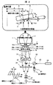
はじめに図2を用いてナノインプリントによるパターン形成手順について説明する。この図は、光硬化型樹脂を用いた場合の配線パターン形成方法を模式的に説明する図である。ウェハ1には、配線パターン14が形成されている。その表面に上層の配線膜15を形成し、さらに、光硬化型樹脂2を塗布する(I)。次に、パターンが形成された金型12をウェハ1上方から接近させ、接触する前に、金型12とウェハ1の位置合わせ(アライメント)をした後に、両者を相対的に押し付けてパターンを形成する(II)。金型12は、石英でできており、光を透過する。金型12を押し付けた後に、金型12背面から紫外線を照射して光硬化型樹脂膜2を硬化させる(III) 。金型12を除去し、凹パターンの底に残るベース層を除去すると、樹脂パターン16が形成されている(IV)。この樹脂パターン16をマスクとして下地の配線膜をエッチングすれば配線パターン17が形成される(V)。
First, a pattern formation procedure by nanoimprint will be described with reference to FIG. This figure is a diagram schematically illustrating a wiring pattern forming method in the case of using a photocurable resin. A wiring pattern 14 is formed on the
以上の手順を実行可能な本発明の実施例を、図1を用いて説明する。図1は、ナノインプリントを用いた半導体デバイス製造用のパターン形成装置、すなわち、リソグラフィ装置の基本構成を示している。パターンを転写するウェハ1表面には樹脂が塗布され、ステージ3に保持される。このステージ3は、図の一軸方向(X)のほか、紙面に垂直な方向(Y)と、XY面内の回転(YAW)の位置決めが可能な機構を備えている。ステージ3の位置は、レーザ測長器4により計測され、ステージ駆動手段により所定の位置に移動される。
An embodiment of the present invention capable of executing the above procedure will be described with reference to FIG. FIG. 1 shows a basic configuration of a pattern forming apparatus for manufacturing a semiconductor device using nanoimprint, that is, a lithography apparatus. Resin is applied to the surface of the
また、ステージ3の上方には、ウェハ1に転写するパターンが形成された金型12を搭載した金型ステージ11が設置されている。金型ステージ11は、上下方向(Z)に位置決めが可能な構成をとっており、ウェハ基板までの距離を測定できるZセンサ13と、ウェハ1と接触後の荷重を測定可能な荷重センサ(図示せず)を備えている。Zセンサ13としては、レーザ測長器,静電容量型ギャップセンサ等を用いることができる。また、金型ステージの複数の位置にZセンサを設けることにより、金型と基板との平行度を確保しながら金型を基板に押し付けることができる。
Further, a
金型12は、透明な基板、例えば、石英やガラスでできており、光を透過するようになっている。また、ウェハ1と金型12のサイズは、同じでもよいし、金型12のサイズをウェハ1の数分の一としてもよい。数分の一とした場合は、従来のステッパ装置のようにステップ移動しながらパターンを転写して、ウェハ全面にパターンを形成することになる。
The
さらに上方には、水銀ランプ10aが備えられており、破線で示す光路をたどり照明光学系10bを透過して並行光に変換した照明光が、金型12を透過して光硬化型樹脂膜2を照明する。この照明は、図示しないシャッタにより露光量や露光時間を制御できる。
Further above, a
このステージ3の下方には、ウェハ1裏面に形成された裏面アライメントマーク7の位置を検出する裏面位置検出器6a,6bがある。この裏面位置検出器6は、装置基準位置に固定されており、装置基準の絶対位置を測定する。一方、ステージ3上方には、金型のパターン形成面の位置を検出する金型位置検出器8a,8bがある。この金型位置検出器8a,8bは、金型が下降してウェハ1と接触する直前、例えば、10μm上空で停止した位置から、接触するまでの領域において金型12の表面に予め形成されている金型アライメントマーク12bの位置を金型位置検出器8a,8bを用いて測定できる。検出可能な位置は、金型の面内方向に加え、高さ方向についても可能なものである。本位置検出手段8a,8bの構成と機能については、後述する。さらに、この金型位置検出器8a,
8bは、装置の基準位置に固定されており、金型の装置基準の絶対位置を測定する。また、ウェハ1は、Si基板に限らず、GaAs基板,ガラス基板、またはプラスチック基板であっても良い。
Below the
8b is fixed to the reference position of the apparatus, and measures the absolute position of the apparatus reference of the mold. Further, the
裏面位置検出器6と金型位置検出器8は、それぞれ独立した位置検出器であるため、基準位置を校正する必要がある。校正用チップ9は、その校正のために用いる手段である。本チップの構成,機能に関する詳細は、後述する。
Since the back surface position detector 6 and the mold position detector 8 are independent position detectors, it is necessary to calibrate the reference position. The
次に、主要な機能の詳細について説明する。まず、ウェハ裏面位置検出器6a,6bについて説明する。図3に示すように、ウェハ1が設定基準面から角度θだけ傾いている状態においては、ウェハ裏面に設けられた裏面アライメントマーク7の実際の位置(基準位置からの距離δ)と該裏面アライメントマーク7に対応するウェハ表面上の真の位置(基準位置からの距離ω)との間には、ウェハ1の厚さをdとした場合、dsinθ なるずれが生じることになる。したがって、該裏面アライメントマーク7の実際の位置(距離δ)を検出して、その検出値をそのままウェハ表面上での真の位置(距離ω)とする場合には、当然のことながら、位置検出誤差εが生じることとなる。例えば、ウェハの厚さdを600μm、ウェハの傾き角θを5秒とすると、誤差量εは、約15nmとなる。この値は、
10nmというような厳しいアライメント精度が要求されるような場合においては、もはや無視できない。そこで、この誤差量εを相殺するような偏差分ΔEを位置検出値に含むような、裏面位置検出器6a,6bを用いて、ウェハ裏面に設けられた裏面アライメントマーク7の見かけ上の位置(δ+ΔE)を検出し、この見かけ上の位置がウェハ表面における真の位置(ω)を表わすようにする。すなわち、裏面位置検出器6a,6bによる見かけ上のマーク位置検出結果(δ+ΔE)が裏面アライメントマーク7に対応するウェハ表面上での真の位置(ω)と等しくなるように、つまり、
ω=δ+ΔE ………(1)
なる関係が成立するように、上記の裏面位置検出器6a,6bの各種パラメータを予め選定しておくのである。式(1)の右辺第2項のΔEが、裏面位置検出器6a,6bによる位置検出値に含まれる偏差分であり、この偏差分がウェハの傾き角θの変化に対応して変化する(つまり、ΔE=−ε=−d・sinθ なる関係で変化する)ことによって、ウェハの傾き角の如何によらず、常に、ウェハの傾きに起因して生じる誤差εを相殺し、結果的に、ウェハ裏面に設けられたマーク位置を検出することによって、該マーク位置に対応するウェハ表面上の真の位置を正確に求めることができるようになる。
Next, details of main functions will be described. First, the wafer back
In cases where strict alignment accuracy such as 10 nm is required, it can no longer be ignored. Therefore, the apparent position of the back surface alignment mark 7 provided on the back surface of the wafer using the back
ω = δ + ΔE (1)
Various parameters of the back
図3の下側に、上記したウェハの傾きに起因して生じる位置検出誤差εを相殺するような偏差分ΔEを検出値に含むような位置検出器の一構成例を示し、その位置検出原理について、説明する。図3において、波長λなる2本の光ビーム18a,18bによってウェハ裏面上の裏面アライメントマーク7を照明した時に得られる回折光の位相は、裏面アライメントマーク7の位置δと両照明光の照明位置A,B間での基準面に垂直方向に測った間隔hとに依存して変化する。両照明光間の間隔をL、ウェハの厚さをdとしたとき、上記の照明位置間間隔hとウェハの傾き角θとの間には、図3より、
θ=tan-1(h/L)≒h/L ………(2)
なる関係式が成り立つ。また、ウェハの傾きによる裏面アライメントマーク7の位置δとウェハ表面の真の位置ωとの間のずれ量εに依存する位相差相当分φ(ε)は、裏面アライメントマーク7のピッチをPとして、
φ(ε)=4πε/P ………(3)
となる。一方、ウェハの傾き角θの関数である照明位置間間隔hに起因する位相差相当分
φ(ΔE)は、図3に示した幾何学的関係からして、検出光の波長λと照明位置間間隔hに対して、次式で表わされる。
A configuration example of a position detector that includes a deviation ΔE that cancels out the position detection error ε caused by the tilt of the wafer as described above is shown on the lower side of FIG. Will be described. In FIG. 3, the phase of the diffracted light obtained when the back surface alignment mark 7 on the back surface of the wafer is illuminated by the two
θ = tan −1 (h / L) ≈h / L (2)
The following relational expression holds. Further, the phase difference equivalent φ (ε) depending on the deviation ε between the position δ of the back surface alignment mark 7 due to the tilt of the wafer and the true position ω of the wafer surface is P as the pitch of the back surface alignment mark 7. ,
φ (ε) = 4πε / P (3)
It becomes. On the other hand, the phase difference equivalent φ (ΔE) caused by the interval h between the illumination positions, which is a function of the wafer tilt angle θ, is calculated from the geometric relationship shown in FIG. With respect to the interval h, it is expressed by the following equation.
φ(ΔE)=4πh/λ ………(4)
つまり、式(3)で表わされる位相変化分φ(ε)と式(4)で表わされる位相変化分
φ(ΔE)とが等しくなるように、裏面アライメントマーク7のピッチPと両検出光間の間隔Lを予め選定しておけば、任意のウェハ傾き角における位相ずれを相殺してやることができる。そこで、上記の関係を満足させるような検出光間隔Lについて、式(1)〜式
(4)を連立させて解くと、
L=λ・d/P ………(5)
なる解が得られる。例えば、マークのピッチPを6μm、ウェハの厚さdを600μm、検出光波長λを633nmとすると、ビーム間隔Lを63.3μm とすれば良いことがわかる。そして、このビーム間隔Lは、ウォラストンプリズム20のビーム分離角度ξと対物レンズ19の焦点距離fとによって決められる。つまり、必要なビーム間隔Lが既知の場合には、次式によってビーム分離角度ξが決定される。
φ (ΔE) = 4πh / λ (4)
In other words, the pitch P of the back surface alignment mark 7 and the distance between the two detection lights are set so that the phase change φ (ε) represented by Expression (3) is equal to the phase change φ (ΔE) represented by Expression (4). If the interval L is selected in advance, the phase shift at an arbitrary wafer tilt angle can be offset. Therefore, when the detection light interval L that satisfies the above relationship is solved by simultaneous equations (1) to (4),
L = λ · d / P (5)
The following solution is obtained. For example, when the mark pitch P is 6 μm, the wafer thickness d is 600 μm, and the detection light wavelength λ is 633 nm, it is understood that the beam interval L may be 63.3 μm. The beam interval L is determined by the beam separation angle ξ of the
ξ=1/(2f) ………(6)
すなわち、このような分離角度ξを有するウォラストンプリズムを用いれば良いことになる。
ξ = 1 / (2f) (6)
That is, a Wollaston prism having such a separation angle ξ may be used.
さて、位置ωを求めるには、二点A,Bを照明する光の位相差φを検出すればよい。この検出方法について説明する。 In order to obtain the position ω, the phase difference φ of the light that illuminates the two points A and B may be detected. This detection method will be described.
波長がわずかに異なる二つの周波数(ν1,ν2)の光を直線偏光の形で出射するレーザ光源23を用いる。該光源からの光ビーム45は、ビームスプリッタ22により二つに分割される。分割された一方の光ビームは偏光子25に入射して、そこでヘテロダイン干渉を生じる。この干渉光を光検出器26によって検出することによって、基準となる参照信号Sr が得られる。分割された他方のビームは、ウォラストンプリズム20に入射し、そこで、P偏光(周波数ν1)のビーム18aとS偏光(周波数ν2)のビーム18bとに分離される。分離されたビーム18a,18bは、対物レンズ19によって並行ビームに変換され、それぞれ試料裏面上の二点A,Bを照射する。両ビームの照射点A,B間の間隔はLである。このとき、照射点A,Bから生じる回折光のうち、−1次光30a,31aと+1次光30b,31bのみに着目すると、これら1次回折光の位相は、すでに述べたように、裏面アライメントマーク7の位置と試料1の傾き角とによって変化する。この位相変化分φは、同図の下方に示すように、光検出器26からの参照信号Sr と検出器29からの検出信号Sd との位相差として求めることができる。+1次回折光30a,30bと−1次回折光30a,31bとは、対物レンズ19により平行ビームとされ、フーリェ変換面において偏光ビームスプリッタ21を用いることによって、一方の照射点からの+1次回折光(例えば、照射点Bからの+1次回折光31b)と他方の照射点からの−1次回折光(例えば、照射点Aからの−1次回折光30a)とを選び取る。この選び取ったビーム31bと30aを集光レンズ24によって集光し、両ビームが交差する点にウォラストンプリズム27を置くことによってヘテロダイン干渉を生じさせ、この干渉光を偏光子28を介して光検出器29により検出する。得られる信号は、図3の左下に示すように、検出信号Sd と参照信号Sr であり、これらの間の位相差φは、
φ=4π/P(δ+ε) ………(7)
ということになり、仮にウェハが傾いた場合においても、この位相差φを検出すればウェハ裏面の位置を検出しながら、ウェハ表面の正しい位置が検出できることになる。
A laser light source 23 that emits light of two frequencies (ν 1 , ν 2 ) having slightly different wavelengths in the form of linearly polarized light is used. The
φ = 4π / P (δ + ε) (7)
Thus, even if the wafer is tilted, if the phase difference φ is detected, the correct position of the wafer surface can be detected while detecting the position of the back surface of the wafer.
このようにすることによって、敢えてウェハ1の傾き角を検出するための傾き検出器を設けること無くして、ウェハ裏面上に設けられたマークの位置を検出して、ウェハ表面上における所望のパターン形成位置を精度良く求めることが可能となる。
In this way, the position of the mark provided on the back surface of the wafer is detected without providing an inclination detector for detecting the inclination angle of the
なお、上記の裏面アライメントマーク7の形成方法としては、通常のエッチングを用いて段差を形成してもよいが、レーザマーカを利用する簡便な方法もある。 In addition, as a formation method of said back surface alignment mark 7, although a level | step difference may be formed using normal etching, there also exists a simple method using a laser marker.
次に、金型位置検出器8a,8bの機能について説明する。図5に示したように、金型位置検出器8a,8bは、金型ステージ11がパターン転写位置近傍に来たときに金型の面内方向の位置検出が可能となる。この位置で焦点が合うような検出光学系を適用した例を図6を用いて説明する。金型の転写パターン12aが形成されている表面の一部に金型アライメントマーク12bを形成する。この金型アライメントマーク12bは、光学的にコントラストを高く取れるようにクロム膜を蒸着して形成してある。形状は、図6に示すようなライン&スペースパターンが望ましい。照明光にはHeNeレーザ(波長633
nm)の光を用いる。図10に示すように、金型アライメントマーク12bから生じる反射±1次回折光のみを空間フィルタ44により選択して集光し、金型位置検出器8a,
8bに備えられた撮像センサ(図7参照)の受像面上にこの金型アライメントマーク12bの光学像32が結像する。さらに、この撮像センサには、基準面33があり、この面から光学像32までの距離xを検出することにより、金型アライメントマーク12bの絶対位置検出が可能となる。例えば、金型アライメントマークのラインを1μm、スペースを1μm(ピッチ2μm)、ラインを5本とすれば、数nmの分解能の絶対位置検出が可能な設計ができる。なお、本金型位置検出では、転写する転写パターン12aと金型アライメントマーク12bは、同一平面上に存在するので、ウェハ裏面位置検出のように、金型
12の厚さの影響を受けることはない。
Next, functions of the
nm) light. As shown in FIG. 10, only the reflection ± first-order diffracted light generated from the
An
次に、金型の高さ方向の位置検出方法について図9,図10を用いて説明する。位置検出光にHeNeレーザ波長633nmの光を用いる。この光は、平行ビームとして出射され、金型アライメントマーク12bを落射照明する。このマークからの回折光のうち、正反射する0次回折光42を用いる。この0次回折光は、空間フィルタ44により選択される。この反射0次回折光は、干渉計41により参照光と干渉して光検出器40により金型アライメントマーク12bの高さ位置が位置検出器8aの基準位置に対して検出される。
Next, a method for detecting the position of the mold in the height direction will be described with reference to FIGS. Light with a HeNe laser wavelength of 633 nm is used as position detection light. This light is emitted as a parallel beam and illuminates the
金型アライメントマーク12bには、位置検出光が透過しないように反射膜が形成されており、下方にあるウェハ基板等からの反射光の影響を排除している。このような構成をとることにより、金型位置検出器8aひとつで金型の面内方向の位置と、高さ方向位置の二つの情報が得られるという効果がある。反射膜の材料は、マークと同じクロムでもよいし、その他の金属でもよい。
A reflection film is formed on the
本金型位置検出器8は、金型上に最低3箇所設けられており、三つの異なる位置での金型の高さ情報より、金型の傾きを制御し、ウェハ基板に対して平行に上下動することができる。こうすることにより、ウェハ基板上に塗布される樹脂の影響を受けることなく金型をウェハに押し付けることができるので、押し付けむらによる樹脂膜へのパターン形成むらを低減できる。 The present mold position detector 8 is provided at least at three locations on the mold, and controls the inclination of the mold based on the height information of the mold at three different positions, and is parallel to the wafer substrate. Can move up and down. By doing so, the mold can be pressed against the wafer without being affected by the resin applied on the wafer substrate, so that uneven pattern formation on the resin film due to uneven pressing can be reduced.
次にステージ3の上面にある校正用チップ9の機能について説明する。本チップは、裏面位置検出器6a,6bと金型位置検出器8a,8bとの相対位置を構成するために備えたチップである。本チップの厚さは、ウェハ1と実質的に同じであり、表面には、金型用アライメントマーク9aが形成され、裏面には、裏面アライメントマーク9bが形成されている。さらに、この校正用チップ9は、図1,図4,図5に記載のようにステージ3の所定の位置に固定されている。
Next, the function of the
まず、この校正用チップ9の使用方法について図4を用いて説明する。金型12をロードする前に、裏面位置検出器6a,6bと金型位置検出器8a,8bの位置測定可能な領域にステージ3を移動して停止させる。この状態で、校正用チップに形成された上下二つのマーク9a,9bをそれぞれの位置検出器6a,8aを用いて基準位置からの距離として位置を測定する。各測定値、例えば、金型位置検出器8aの検出位置Cと裏面位置検出器6aの検出位置Dを等しくするように校正して、金型位置検出器8aと裏面位置検出器6aの校正を行う。図4では装置左側の位置検出器を校正する様子を示しているが、他の位置検出器に対してもこの校正の後にステージを右側の位置検出器の領域に合わせて、同様の方法により校正すればよい。
First, a method of using the
次に金型位置検出器8aの高さ方向位置検出値の校正方法について説明する。パターン形成装置にウェハ基板と同じ厚さのダミー基板43をロードし、金型を下げて行きながら、高さ位置検出器13を用いて金型の高さ方向の位置を検出する。金型がダミー基板と接触したら、金型位置検出器8aの高さ方向の値を検出して、この位置を接触位置として記憶することにより、校正が行える。実際の転写の際には、ウェハ基板上には樹脂が塗布されていることから、高さ位置検出器13は、正確な位置を検出できず、問題となるが、本発明によれば、樹脂の影響を受けず、精密な高さ位置を検出でき、望ましい。
Next, a method of calibrating the height position detection value of the
以上述べてきたナノインプリントによる半導体デバイスのパターン形成方法、及び、その方法を実行するためのリソグラフィ装置の各機能を用いてパターン形成する手順について、さらに詳しく説明する。 The semiconductor device pattern formation method by nanoimprint described above and the procedure for pattern formation using each function of the lithography apparatus for executing the method will be described in more detail.
まず、ナノインプリントを用いたパターン形成装置の電源を投入し、装置を立ち上げる。図4に示すように、金型12をロードする前に、各位置検出器、すなわち、金型用位置検出器8a,8b、裏面位置検出器6a,6bの校正を行う。この校正方法は、既に述べたとおりである。
First, a pattern forming apparatus using nanoimprint is turned on and the apparatus is started up. As shown in FIG. 4, before loading the
次に、図1に示すように、金型12と、配線パターン14の上に配線膜15と光硬化型樹脂を所定の膜厚で塗布したウェハ1をロードする。このウェハ1の裏面には、位置検出用の裏面アライメントマーク7が予め形成されている。マークの形状は、既に述べたように所定の形状を有するライン&スペースパターンが望ましい。この裏面アライメントマーク7は、所定の間隔を持って形成されており、ステージのウェハチャックに設けられた開口46の位置に合わせて載置する。
Next, as shown in FIG. 1, a
次に、ウェハステージ3を所定の位置に移動した後に金型12をウェハ1上方から接近させ、金型位置検出器8の高さ位置検出機能を用いて、金型12がウェハ最上面に形成された光硬化型樹脂膜2と接触する直前、例えば、10μm程度上空で一旦停止する。この状態で、金型位置検出器8a,8bと裏面位置検出器6a,6bを用いて金型12とウェハ1の相対位置を所定の関係にアライメントする。この相対位置を保持したまま、金型
12をウェハ1に、図示しない荷重センサの出力を利用し、所定の押し付け力を保持したまま押し付ける。
Next, after moving the
その後、最上部にある水銀ランプ10のシャッタを開放して所定の露光量を持って、金型12を通してパターンを露光した後、金型12を上部に引き上げて樹脂パターン16を形成する。
Thereafter, the shutter of the
ここで、加圧方法に関して、上述した複数のZセンサを設ける方法とは異なる次の方法を用いてもよい。図8に図示するように金型ステージ11、と紫外線を透過するガラス製のビューポート39に仕切られた金型上部チャンバ34、と金型ステージ11よりも下の部分に配置されたエリアであるステージチャンバ35を設け、これらエリアに真空ポンプ
38に接続した真空ライン36が取り付けられた装置を用いることで圧力差による加圧を実現する。具体的には、はじめにバルブ37aを閉じ、バルブ37b開いた状態で金型上部チャンバ34とステージチャンバ35を脱気の後、位置合わせを行い、金型ステージ
11を下降させる。次にバルブ37bを閉じ、バルブ37aを開放することで金型上部の上部チャンバ34とステージチャンバ35間に圧力差が生じ金型上部前面に大気圧が印加される。この様にすることで金型上部前面に均等に圧力が印加され、金型のたわみなどにより生ずる転写樹脂の厚さムラが解消される。ここでは大気圧を印加したが、代わりに高圧のガスを導入してもよい。
Here, regarding the pressurizing method, the following method different from the method of providing the plurality of Z sensors described above may be used. As shown in FIG. 8, the
金型12がウェハ1より小さい場合、次の位置へステージ3をステップ移動して、金型12をウェハ1上方から接近させ、Zセンサ13を用いて、金型12がウェハ最上面に形成された光硬化型樹脂膜2と接触する直前、例えば、10μm程度上空で一旦停止する。この状態で、金型位置検出器8a,8bと裏面位置検出器6a,6bを用いて金型12とウェハ1の相対位置を所定の関係にアライメントする。この相対位置を保持したまま、金型12をウェハ1に、図示しない荷重センサの出力を利用し、所定の押し付け力を保持したまま押し付ける。以上の動作をウェハ1全面にパターン転写するまで繰り返す。
If the
その後、この樹脂パターン16をマスクとして下地の配線膜をエッチングすれば配線パターン17が形成される。
Thereafter, the
以上、述べてきたようにナノインプリントを半導体デバイスの製造工程のひとつであるリソグラフィに適用するに当り問題となるアライメント誤差は、ウェハ1の表面に形成される樹脂膜と金型の接触に伴う、樹脂の不均一な屈折率分布による位置検出誤差や、樹脂が押し付けられて面内に広がるに伴って発生する面内方向の力による不均一な位置ずれが主要因である。本実施例で説明したウェハ裏面アライメントと、金型のアライメント方式を用いて相対的なアライメントを行い、相対位置を保持したまま両者を押し付けてパターンを形成することにより、上述のアライメント誤差の問題を解決することができる。
As described above, the alignment error, which is a problem when applying nanoimprinting to lithography, which is one of the manufacturing processes of a semiconductor device, is a resin caused by the contact between the resin film formed on the surface of the
さらに、金型12が光学的に不透明な場合、金型位置検出器8に裏面位置検出器6と同様な基板の傾きキャンセル機能を設ければよいことは、敢えて詳細を述べなくても明らかである。
Further, when the
本実施例のパターン形成装置を用いて製造するデバイスは、半導体の他にも適用することができる。例えば、最近盛んに検討されている3次元フォトニック結晶は、周期的な構造に、それを乱す人為的な構造を含ませることにより、発光特性を制御できるという特性を持たせることができる(応用物理学会誌、第74巻、2月号、p147〜p159)。このような3次元構造物を製造する技術として用いることができる。しかも、従来のリソグラフィ技術を用いるよりはるかに安価にできることから、産業上の応用効果は大きいといえる。 A device manufactured using the pattern forming apparatus of this embodiment can be applied to a semiconductor as well. For example, a three-dimensional photonic crystal that has been actively studied recently can have a characteristic that the light emission characteristic can be controlled by including an artificial structure that disturbs the periodic structure (application). Journal of Physics Society, Volume 74, February, p147-p159). It can be used as a technique for manufacturing such a three-dimensional structure. In addition, since it can be made much cheaper than the conventional lithography technique, it can be said that the industrial application effect is great.
1…ウェハ、2…光硬化型樹脂膜、3…ステージ、4…レーザ測長器、5…ステージ駆動手段、6…ウェハ裏面位置検出器、7…ウェハ裏面アライメントマーク、8…金型位置検出器、9…校正チップ、10…照明光学系、11…金型ステージ、12…金型、12a…転写パターン、12b…金型アライメントマーク、13…Zセンサ、14,17…配線パターン、15…配線材料膜、16…樹脂パターン、18…裏面膜照明光、19…対物レンズ、20,27…ウォラストンプリズム、21,22…偏光ビームスプリッタ、23…レーザ光源、24…集光レンズ、25,28…偏光子、26,29,40…光検出器、
30…A点から発生する1次回折光、31…B点から発生する1次回折光、32…金型アライメントマークの光学像、33…金型位置検出器の撮像面に形成された基準面、34…金型上部チャンバ、35…ステージチャンバ、36…真空ライン、37a,37b…バルブ、38…真空ポンプ、39…ビューポート、41…干渉計、42…0次回折光、43…ダミー基板、44…空間フィルタ。
DESCRIPTION OF
30... First order diffracted light generated from point A, 31... First order diffracted light generated from point B, 32... Optical image of mold alignment mark, 33... Reference plane formed on imaging surface of mold position detector, 34 ... Die upper chamber, 35 ... Stage chamber, 36 ... Vacuum line, 37a, 37b ... Valve, 38 ... Vacuum pump, 39 ... Viewport, 41 ... Interferometer, 42 ... 0th order diffracted light, 43 ... Dummy substrate, 44 ... Spatial filter.
Claims (12)
複数の位置で金型と樹脂膜が塗布された基板との間の距離を測定する工程と、
金型と樹脂膜が塗布された基板が接触する直前で停止する工程と、
該樹脂膜を塗布した基板の裏面に形成された基板アライメントマークに基板の裏面側から光を照明し、その回折光を用いて基板アライメントマークの位置を検出する工程と、
金型に形成された反射膜を有する金型アライメントマークに金型の裏面側から光を照明し、その回折光を用いて金型アライメントマークの位置を検出する工程と、
検出した基板アライメントマーク及び金型アライメントの位置を用いて、金型と樹脂膜が塗布された基板とのパターンを形成する面内における相対的な位置を位置合わせする工程と、
前記相対位置を保持したまま金型を樹脂膜が塗布された基板に押し付ける工程と、
を含むことを特徴とするパターン形成方法。 In a pattern formation method using nanoimprint in which a mold in which an uneven pattern is formed is pressed against a substrate coated with a resin film to form a pattern,
Measuring a distance between a mold and a substrate coated with a resin film at a plurality of positions;
A step of stopping just before the mold and the substrate coated with the resin film come into contact with each other;
Illuminating the substrate alignment mark formed on the back side of the substrate coated with the resin film with light from the back side of the substrate, and detecting the position of the substrate alignment mark using the diffracted light;
Illuminating a mold alignment mark having a reflective film formed on the mold with light from the back side of the mold, and detecting the position of the mold alignment mark using the diffracted light;
Using the detected substrate alignment mark and the position of the mold alignment, aligning the relative position in the surface forming the pattern between the mold and the substrate coated with the resin film;
Pressing the mold against the substrate coated with the resin film while maintaining the relative position;
A pattern forming method comprising:
金型アライメントマークが一定周期のピッチで金型上に形成されたラインアンドスペースパターンであり、
金型と樹脂膜が塗布された基板との間の距離を測定する工程で、レーザを光源としたビームを金型アライメントマークに照明し、該金型アライメントマークから生じる反射回折光のうち、0次回折光を用いて該金型の該樹脂を塗布された基板との距離を計測することを特徴とするパターン形成方法。 In the pattern formation method of Claim 1 ,
The mold alignment mark is a line-and-space pattern formed on the mold with a constant pitch,
In step mold and the resin film to measure the distance between the substrate coated, the beams of laser light source illuminates the mold alignment mark, among the reflected diffracted light generated from the mold alignment mark, 0 A pattern forming method, characterized in that the distance of the mold from the substrate coated with the resin is measured using next diffracted light.
金型を樹脂膜が塗布された基板に押し付ける工程で、前記相対位置を保持しかつ、複数の位置で測定された金型と基板との距離に基づき金型と基板の平行を確保し、金型を樹脂膜が塗布された基板に押し付けることを特徴とするパターン形成方法。 In the pattern formation method of Claim 1,
In the step of pressing the mold against the substrate coated with the resin film, the mold is held parallel to the mold based on the distance between the mold and the substrate measured at a plurality of positions while maintaining the relative position. pattern forming method a mold is the resin film and wherein the Turkey pressed against the substrate coated.
樹脂膜が塗布された基板を保持するための基板ステージと、基板ステージを所定の位置に移動可能なステージ駆動手段と、金型を保持するための金型ステージと、
樹脂を塗布した基板の裏面に形成された基板アライメントマークに基板の裏面側から光を照明し、その回折光を用いて基板アライメントマークの位置を検出する裏面位置検出器と、
金型に形成された反射膜を有する金型アライメントマークに金型の裏面側から光を照明し、その回折光を用いて金型アライメントマークの位置を検出する金型位置検出器とを備え、
裏面検出器及び金型位置検出器の検出結果に基づき基板と金型との相対的な位置を位置合わせする手段を有することを特徴とするパターン形成装置。 In a pattern forming apparatus for forming a pattern by pressing a mold having a concavo-convex pattern against a substrate coated with a resin film,
A substrate stage for holding a substrate coated with a resin film, a stage driving means capable of moving the substrate stage to a predetermined position, a mold stage for holding a mold,
A back surface position detector that illuminates light from the back surface side of the substrate to the substrate alignment mark formed on the back surface of the substrate coated with resin, and detects the position of the substrate alignment mark using the diffracted light ;
A mold alignment mark having a reflective film formed on the mold is illuminated with light from the back side of the mold, and includes a mold position detector that detects the position of the mold alignment mark using the diffracted light ,
A pattern forming apparatus comprising means for aligning the relative positions of a substrate and a mold based on detection results of a back surface detector and a mold position detector.
Priority Applications (4)
| Application Number | Priority Date | Filing Date | Title |
|---|---|---|---|
| JP2006014525A JP4736821B2 (en) | 2006-01-24 | 2006-01-24 | Pattern forming method and pattern forming apparatus |
| CNB2007100022640A CN100536073C (en) | 2006-01-24 | 2007-01-17 | Pattern forming method and pattern forming system |
| EP07001424A EP1811337A3 (en) | 2006-01-24 | 2007-01-23 | Pattern forming method and pattern forming system |
| US11/626,402 US7745237B2 (en) | 2006-01-24 | 2007-01-24 | Pattern forming method and pattern forming system |
Applications Claiming Priority (1)
| Application Number | Priority Date | Filing Date | Title |
|---|---|---|---|
| JP2006014525A JP4736821B2 (en) | 2006-01-24 | 2006-01-24 | Pattern forming method and pattern forming apparatus |
Publications (2)
| Publication Number | Publication Date |
|---|---|
| JP2007200953A JP2007200953A (en) | 2007-08-09 |
| JP4736821B2 true JP4736821B2 (en) | 2011-07-27 |
Family
ID=38051361
Family Applications (1)
| Application Number | Title | Priority Date | Filing Date |
|---|---|---|---|
| JP2006014525A Expired - Fee Related JP4736821B2 (en) | 2006-01-24 | 2006-01-24 | Pattern forming method and pattern forming apparatus |
Country Status (4)
| Country | Link |
|---|---|
| US (1) | US7745237B2 (en) |
| EP (1) | EP1811337A3 (en) |
| JP (1) | JP4736821B2 (en) |
| CN (1) | CN100536073C (en) |
Families Citing this family (36)
| Publication number | Priority date | Publication date | Assignee | Title |
|---|---|---|---|---|
| JP4958614B2 (en) * | 2006-04-18 | 2012-06-20 | キヤノン株式会社 | Pattern transfer apparatus, imprint apparatus, pattern transfer method, and alignment apparatus |
| JP4848832B2 (en) * | 2006-05-09 | 2011-12-28 | 凸版印刷株式会社 | Nanoimprint apparatus and nanoimprint method |
| KR101261606B1 (en) * | 2006-05-09 | 2013-05-09 | 삼성디스플레이 주식회사 | Apparatus for manufacturing a display panel and method for manufacturing the same |
| CN101600993B (en) | 2007-02-06 | 2013-01-16 | 佳能株式会社 | Imprint method and imprint apparatus |
| US7837907B2 (en) * | 2007-07-20 | 2010-11-23 | Molecular Imprints, Inc. | Alignment system and method for a substrate in a nano-imprint process |
| JP5473266B2 (en) * | 2007-08-03 | 2014-04-16 | キヤノン株式会社 | Imprint method, substrate processing method, and semiconductor device manufacturing method by substrate processing method |
| KR100929883B1 (en) * | 2007-11-16 | 2009-12-04 | 한국전기연구원 | Nano exposure machine and exposure method for high resolution transfer of cylindrical mold substrate and active posture control |
| JPWO2009153925A1 (en) * | 2008-06-17 | 2011-11-24 | 株式会社ニコン | Nanoimprint method and apparatus |
| JP5517423B2 (en) | 2008-08-26 | 2014-06-11 | キヤノン株式会社 | Imprint apparatus and imprint method |
| JP4603101B1 (en) * | 2008-12-24 | 2010-12-22 | パナソニック株式会社 | Method for manufacturing diffractive optical element and diffractive optical element |
| NL2003871A (en) | 2009-02-04 | 2010-08-05 | Asml Netherlands Bv | Imprint lithography. |
| JP5476796B2 (en) * | 2009-05-27 | 2014-04-23 | 大日本印刷株式会社 | Nanoimprint mold and pattern forming method |
| NL2006454A (en) * | 2010-05-03 | 2011-11-07 | Asml Netherlands Bv | Imprint lithography method and apparatus. |
| JP5652105B2 (en) * | 2010-10-13 | 2015-01-14 | 株式会社ニコン | Exposure equipment |
| JP5323882B2 (en) * | 2011-04-08 | 2013-10-23 | 株式会社日立産機システム | Pattern transfer apparatus and pattern transfer method |
| WO2012149029A2 (en) * | 2011-04-25 | 2012-11-01 | Molecular Imprints, Inc. | Optically absorptive material for alignment marks |
| JP6061524B2 (en) * | 2011-08-11 | 2017-01-18 | キヤノン株式会社 | Imprint apparatus and article manufacturing method |
| JP6029268B2 (en) * | 2011-09-12 | 2016-11-24 | キヤノン株式会社 | Imprint apparatus and article manufacturing method using the same |
| JP6019685B2 (en) * | 2012-04-10 | 2016-11-02 | 大日本印刷株式会社 | Nanoimprint method and nanoimprint apparatus |
| JP2014017407A (en) * | 2012-07-10 | 2014-01-30 | Toyota Motor Corp | Semiconductor device manufacturing method |
| JP6412317B2 (en) | 2013-04-24 | 2018-10-24 | キヤノン株式会社 | Imprint method, imprint apparatus, and article manufacturing method |
| JP6395352B2 (en) * | 2013-07-12 | 2018-09-26 | キヤノン株式会社 | Imprint apparatus, imprint method, and article manufacturing method using the same |
| DE102014011954B4 (en) * | 2013-08-28 | 2024-12-24 | Jenoptik Optical Systems Gmbh | Device for measuring a power density distribution of a radiation source |
| JP5745129B2 (en) * | 2014-04-02 | 2015-07-08 | キヤノン株式会社 | Imprint apparatus and imprint method |
| JP6429573B2 (en) * | 2014-10-03 | 2018-11-28 | キヤノン株式会社 | Imprint apparatus, imprint method, and article manufacturing method |
| JP2015135975A (en) * | 2015-02-23 | 2015-07-27 | キヤノン株式会社 | Imprint apparatus and imprint method |
| JP6495465B2 (en) * | 2015-09-30 | 2019-04-03 | 富士フイルム株式会社 | Method for producing mold, method for producing pattern sheet, method for producing electroformed mold, and method for producing mold using electroformed mold |
| JP6748461B2 (en) * | 2016-03-22 | 2020-09-02 | キヤノン株式会社 | Imprint apparatus, method of operating imprint apparatus, and article manufacturing method |
| JP6700936B2 (en) | 2016-04-25 | 2020-05-27 | キヤノン株式会社 | Imprint apparatus, imprint method, and article manufacturing method |
| JP6207671B1 (en) * | 2016-06-01 | 2017-10-04 | キヤノン株式会社 | Pattern forming apparatus, substrate arranging method, and article manufacturing method |
| CN105974731B (en) * | 2016-07-25 | 2020-01-03 | 京东方科技集团股份有限公司 | Stamping plate, detection method and detection device |
| TWI825023B (en) * | 2017-08-24 | 2023-12-11 | 日商索尼股份有限公司 | Light modeling device, lighting control method and lighting control program |
| KR20190033283A (en) * | 2017-09-21 | 2019-03-29 | 삼성전자주식회사 | Metasurface optical element and method of manufacturing the same |
| JP7310472B2 (en) | 2019-09-13 | 2023-07-19 | 信越化学工業株式会社 | Manufacturing method of reflective mask blank |
| JP7458161B2 (en) * | 2019-09-24 | 2024-03-29 | 東京エレクトロン株式会社 | Inspection device control method and inspection device |
| KR102520642B1 (en) * | 2020-12-29 | 2023-04-11 | 주식회사 기가레인 | Transfer apparatus capable of pattern alignment |
Family Cites Families (22)
| Publication number | Priority date | Publication date | Assignee | Title |
|---|---|---|---|---|
| JP3019489B2 (en) * | 1990-07-23 | 2000-03-13 | 株式会社日立製作所 | Method for manufacturing semiconductor device |
| US5200798A (en) * | 1990-07-23 | 1993-04-06 | Hitachi, Ltd. | Method of position detection and the method and apparatus of printing patterns by use of the position detection method |
| JPH0580530A (en) * | 1991-09-24 | 1993-04-02 | Hitachi Ltd | Production of thin film pattern |
| JPH0729815A (en) * | 1993-07-14 | 1995-01-31 | Ushio Inc | Alignment device for mask and work and alignment method using the same |
| US6309580B1 (en) * | 1995-11-15 | 2001-10-30 | Regents Of The University Of Minnesota | Release surfaces, particularly for use in nanoimprint lithography |
| US5772905A (en) * | 1995-11-15 | 1998-06-30 | Regents Of The University Of Minnesota | Nanoimprint lithography |
| US5669303A (en) * | 1996-03-04 | 1997-09-23 | Motorola | Apparatus and method for stamping a surface |
| JPH09312248A (en) * | 1996-05-21 | 1997-12-02 | Nikon Corp | Exposure equipment |
| JP2000323461A (en) * | 1999-05-11 | 2000-11-24 | Nec Corp | Fine pattern forming device, its manufacture, and method of forming the same |
| US6403663B1 (en) * | 1999-09-20 | 2002-06-11 | North Carolina State University | Method of making foamed materials using surfactants and carbon dioxide |
| JP2001235877A (en) * | 1999-12-14 | 2001-08-31 | Sony Chem Corp | Exposure method |
| WO2002067055A2 (en) * | 2000-10-12 | 2002-08-29 | Board Of Regents, The University Of Texas System | Template for room temperature, low pressure micro- and nano-imprint lithography |
| US6946322B2 (en) * | 2002-07-25 | 2005-09-20 | Hrl Laboratories, Llc | Large area printing method for integrating device and circuit components |
| JP4287103B2 (en) * | 2002-08-20 | 2009-07-01 | 株式会社トプコン | Exposure method and exposure apparatus |
| TWI297045B (en) * | 2003-05-07 | 2008-05-21 | Microfabrica Inc | Methods and apparatus for forming multi-layer structures using adhered masks |
| JP2004335808A (en) * | 2003-05-08 | 2004-11-25 | Sony Corp | Pattern transfer device, pattern transfer method and program |
| JP4217551B2 (en) * | 2003-07-02 | 2009-02-04 | キヤノン株式会社 | Fine processing method and fine processing apparatus |
| JP4478424B2 (en) * | 2003-09-29 | 2010-06-09 | キヤノン株式会社 | Microfabrication apparatus and device manufacturing method |
| JP2005116978A (en) * | 2003-10-10 | 2005-04-28 | Sumitomo Heavy Ind Ltd | Nano imprint equipment and method |
| JP2005268675A (en) * | 2004-03-22 | 2005-09-29 | Canon Inc | Fine pattern forming apparatus and semiconductor device manufacturing method |
| JP2006013400A (en) * | 2004-06-29 | 2006-01-12 | Canon Inc | Method and apparatus for detecting relative displacement between two objects |
| US7463337B2 (en) * | 2005-12-30 | 2008-12-09 | Asml Netherlands B.V. | Substrate table with windows, method of measuring a position of a substrate and a lithographic apparatus |
-
2006
- 2006-01-24 JP JP2006014525A patent/JP4736821B2/en not_active Expired - Fee Related
-
2007
- 2007-01-17 CN CNB2007100022640A patent/CN100536073C/en not_active Expired - Fee Related
- 2007-01-23 EP EP07001424A patent/EP1811337A3/en not_active Withdrawn
- 2007-01-24 US US11/626,402 patent/US7745237B2/en not_active Expired - Fee Related
Also Published As
| Publication number | Publication date |
|---|---|
| US7745237B2 (en) | 2010-06-29 |
| EP1811337A3 (en) | 2007-11-07 |
| US20070172967A1 (en) | 2007-07-26 |
| EP1811337A2 (en) | 2007-07-25 |
| JP2007200953A (en) | 2007-08-09 |
| CN101009218A (en) | 2007-08-01 |
| CN100536073C (en) | 2009-09-02 |
Similar Documents
| Publication | Publication Date | Title |
|---|---|---|
| JP4736821B2 (en) | Pattern forming method and pattern forming apparatus | |
| JP4719817B2 (en) | Method, scatterometer, and lithographic apparatus for measuring substrate properties | |
| CN101819384B (en) | Inspection apparatus, lithographic apparatus, lithographic processing cell and inspection method | |
| CN102498441B (en) | Method for measurement and equipment, etching system and lithographic processing cell | |
| JP4897006B2 (en) | Method for providing alignment mark, device manufacturing method, and lithographic apparatus | |
| TWI431439B (en) | Level sensor arrangement for lithographic apparatus and device manufacturing method | |
| JP4672704B2 (en) | Method of measuring substrate overlay error, substrate manufacturing method, and inspection apparatus | |
| JP5288808B2 (en) | Measuring method, inspection apparatus and lithography apparatus | |
| JP4980264B2 (en) | Inspection method, device manufacturing method, inspection apparatus, substrate, mask, lithographic apparatus, and lithography cell | |
| JP4812712B2 (en) | Method for measuring characteristics of substrate and device measuring method | |
| US7869022B2 (en) | Inspection method and apparatus lithographic apparatus, lithographic processing cell, device manufacturing method and distance measuring system | |
| KR101331107B1 (en) | Scatterometer and lithographic apparatus | |
| TWI500094B (en) | Measuring the sub-wavelength section of the target on the substrate | |
| JP4965376B2 (en) | Substrate, inspection apparatus, inspection method, lithographic apparatus, and lithography cell | |
| JP2008258606A (en) | Method for measuring asymmetry of scatterometer, method for measuring overlay error of substrate, and measuring apparatus | |
| JP4875685B2 (en) | Method for determining parameters of target pattern, method for generating library, inspection apparatus, lithographic apparatus, lithography cell, and computer program | |
| CN111051994B (en) | Method for measuring focus performance of lithographic apparatus, patterning apparatus and device, and device manufacturing method | |
| TWI813492B (en) | Sensor apparatus and method for lithographic measurements | |
| TW201312299A (en) | Level sensor configuration for lithography apparatus, lithography apparatus, and device manufacturing method | |
| US11409206B2 (en) | Alignment method and apparatus | |
| NL2020922A (en) | Sensor, lithographic apparatus, and device manufacturing method | |
| TWI428583B (en) | Scatterometer method and apparatus, lithographic apparatus, lithographic processing cell and device manufacturing method | |
| WO2009127322A1 (en) | Focus sensor, inspection apparatus, lithographic apparatus and control system |
Legal Events
| Date | Code | Title | Description |
|---|---|---|---|
| A621 | Written request for application examination |
Free format text: JAPANESE INTERMEDIATE CODE: A621 Effective date: 20080328 |
|
| A977 | Report on retrieval |
Free format text: JAPANESE INTERMEDIATE CODE: A971007 Effective date: 20100708 |
|
| A131 | Notification of reasons for refusal |
Free format text: JAPANESE INTERMEDIATE CODE: A131 Effective date: 20100803 |
|
| A521 | Request for written amendment filed |
Free format text: JAPANESE INTERMEDIATE CODE: A523 Effective date: 20101004 |
|
| A01 | Written decision to grant a patent or to grant a registration (utility model) |
Free format text: JAPANESE INTERMEDIATE CODE: A01 Effective date: 20110405 |
|
| A61 | First payment of annual fees (during grant procedure) |
Free format text: JAPANESE INTERMEDIATE CODE: A61 Effective date: 20110418 |
|
| FPAY | Renewal fee payment (event date is renewal date of database) |
Free format text: PAYMENT UNTIL: 20140513 Year of fee payment: 3 |
|
| LAPS | Cancellation because of no payment of annual fees |