JP4725600B2 - Magneto impedance sensor element - Google Patents
Magneto impedance sensor element Download PDFInfo
- Publication number
- JP4725600B2 JP4725600B2 JP2008151537A JP2008151537A JP4725600B2 JP 4725600 B2 JP4725600 B2 JP 4725600B2 JP 2008151537 A JP2008151537 A JP 2008151537A JP 2008151537 A JP2008151537 A JP 2008151537A JP 4725600 B2 JP4725600 B2 JP 4725600B2
- Authority
- JP
- Japan
- Prior art keywords
- sensor element
- wire
- magnetic amorphous
- amorphous wire
- terminal
- Prior art date
- Legal status (The legal status is an assumption and is not a legal conclusion. Google has not performed a legal analysis and makes no representation as to the accuracy of the status listed.)
- Active
Links
- 239000000758 substrate Substances 0.000 claims description 49
- 238000001514 detection method Methods 0.000 claims description 40
- 239000012212 insulator Substances 0.000 claims description 30
- 230000000630 rising effect Effects 0.000 claims description 3
- 235000012431 wafers Nutrition 0.000 description 23
- 230000000052 comparative effect Effects 0.000 description 19
- 230000035945 sensitivity Effects 0.000 description 14
- 238000005520 cutting process Methods 0.000 description 12
- 239000000463 material Substances 0.000 description 12
- 238000004519 manufacturing process Methods 0.000 description 11
- 238000000034 method Methods 0.000 description 6
- 230000015572 biosynthetic process Effects 0.000 description 5
- 230000000694 effects Effects 0.000 description 5
- 239000000919 ceramic Substances 0.000 description 4
- 239000011810 insulating material Substances 0.000 description 4
- 239000003822 epoxy resin Substances 0.000 description 3
- 239000000696 magnetic material Substances 0.000 description 3
- 230000003071 parasitic effect Effects 0.000 description 3
- 229920000647 polyepoxide Polymers 0.000 description 3
- 239000011248 coating agent Substances 0.000 description 2
- 238000000576 coating method Methods 0.000 description 2
- 238000009833 condensation Methods 0.000 description 2
- 230000005494 condensation Effects 0.000 description 2
- 238000010586 diagram Methods 0.000 description 2
- 238000011156 evaluation Methods 0.000 description 2
- 230000010355 oscillation Effects 0.000 description 2
- 238000000059 patterning Methods 0.000 description 2
- 238000007747 plating Methods 0.000 description 2
- 229920005989 resin Polymers 0.000 description 2
- 239000011347 resin Substances 0.000 description 2
- 238000004544 sputter deposition Methods 0.000 description 2
- 229910019230 CoFeSiB Inorganic materials 0.000 description 1
- VYPSYNLAJGMNEJ-UHFFFAOYSA-N Silicium dioxide Chemical compound O=[Si]=O VYPSYNLAJGMNEJ-UHFFFAOYSA-N 0.000 description 1
- XUIMIQQOPSSXEZ-UHFFFAOYSA-N Silicon Chemical compound [Si] XUIMIQQOPSSXEZ-UHFFFAOYSA-N 0.000 description 1
- 239000000853 adhesive Substances 0.000 description 1
- 230000001070 adhesive effect Effects 0.000 description 1
- 229910045601 alloy Inorganic materials 0.000 description 1
- 239000000956 alloy Substances 0.000 description 1
- PNEYBMLMFCGWSK-UHFFFAOYSA-N aluminium oxide Inorganic materials [O-2].[O-2].[O-2].[Al+3].[Al+3] PNEYBMLMFCGWSK-UHFFFAOYSA-N 0.000 description 1
- 239000004020 conductor Substances 0.000 description 1
- 230000001771 impaired effect Effects 0.000 description 1
- 238000005259 measurement Methods 0.000 description 1
- 229910052751 metal Inorganic materials 0.000 description 1
- 239000002184 metal Substances 0.000 description 1
- 150000002739 metals Chemical class 0.000 description 1
- TWNQGVIAIRXVLR-UHFFFAOYSA-N oxo(oxoalumanyloxy)alumane Chemical compound O=[Al]O[Al]=O TWNQGVIAIRXVLR-UHFFFAOYSA-N 0.000 description 1
- 230000002093 peripheral effect Effects 0.000 description 1
- 230000007261 regionalization Effects 0.000 description 1
- 239000004065 semiconductor Substances 0.000 description 1
- 229910052710 silicon Inorganic materials 0.000 description 1
- 239000010703 silicon Substances 0.000 description 1
- 229910052814 silicon oxide Inorganic materials 0.000 description 1
- 229910000679 solder Inorganic materials 0.000 description 1
- 238000005476 soldering Methods 0.000 description 1
- 238000004804 winding Methods 0.000 description 1
Images


Classifications
-
- G—PHYSICS
- G01—MEASURING; TESTING
- G01R—MEASURING ELECTRIC VARIABLES; MEASURING MAGNETIC VARIABLES
- G01R33/00—Arrangements or instruments for measuring magnetic variables
- G01R33/02—Measuring direction or magnitude of magnetic fields or magnetic flux
-
- G—PHYSICS
- G01—MEASURING; TESTING
- G01R—MEASURING ELECTRIC VARIABLES; MEASURING MAGNETIC VARIABLES
- G01R33/00—Arrangements or instruments for measuring magnetic variables
- G01R33/02—Measuring direction or magnitude of magnetic fields or magnetic flux
- G01R33/06—Measuring direction or magnitude of magnetic fields or magnetic flux using galvano-magnetic devices
- G01R33/063—Magneto-impedance sensors; Nanocristallin sensors
-
- G—PHYSICS
- G01—MEASURING; TESTING
- G01R—MEASURING ELECTRIC VARIABLES; MEASURING MAGNETIC VARIABLES
- G01R33/00—Arrangements or instruments for measuring magnetic variables
- G01R33/12—Measuring magnetic properties of articles or specimens of solids or fluids
- G01R33/18—Measuring magnetostrictive properties
Landscapes
- Physics & Mathematics (AREA)
- Condensed Matter Physics & Semiconductors (AREA)
- General Physics & Mathematics (AREA)
- Chemical & Material Sciences (AREA)
- Engineering & Computer Science (AREA)
- Nanotechnology (AREA)
- Measuring Magnetic Variables (AREA)
- Hall/Mr Elements (AREA)
Description
本発明は、外部磁界に応じて特性が変化する磁性アモルファスワイヤを用いたマグネトインピーダンスセンサ素子に関する。 The present invention relates to a magneto-impedance sensor element using a magnetic amorphous wire whose characteristics change according to an external magnetic field.
磁気方位センサ等に用いられるセンサ素子として、外部磁界に応じて特性が変化する磁性アモルファスワイヤを用いたマグネトインピーダンスセンサ素子(以下、適宜「MIセンサ素子」という。)が開発されている(特許文献1参照)。
かかるMIセンサ素子は、非磁性体からなる基体と、該基体上に保持された磁性アモルファスワイヤと、該磁性アモルファスワイヤが内側を貫通するように形成した被覆絶縁体と、該被覆絶縁体の周囲に形成した検出コイルとを有する。
このような構成のMIセンサ素子は、例えば携帯電話機等の携帯端末機器などに搭載するため、かかる機器の小型化、薄型化の要請に伴い、MIセンサ素子の小型化が要請されている。
As a sensor element used for a magnetic orientation sensor or the like, a magneto-impedance sensor element using a magnetic amorphous wire whose characteristics change according to an external magnetic field (hereinafter referred to as “MI sensor element” as appropriate) has been developed (Patent Literature). 1).
Such an MI sensor element includes a base made of a non-magnetic material, a magnetic amorphous wire held on the base, a coating insulator formed so that the magnetic amorphous wire penetrates the inside, and a periphery of the coating insulator And a detection coil formed on the substrate.
Since the MI sensor element having such a configuration is mounted on, for example, a portable terminal device such as a mobile phone, the MI sensor element is required to be downsized along with a request for downsizing and thinning of the device.
しかしながら、MIセンサ素子の感度を確保するためには、磁性アモルファスワイヤの長さが必要となる。
すなわち、磁性アモルファスワイヤの長さが長いほど、内部に生じる反磁界が小さくなり、反磁界の影響を抑制することができるため、MIセンサ素子の出力を大きくしやすい。また、磁性アモルファスワイヤを長くするほど、その周囲に被覆絶縁体を介して形成する検出コイルの巻き数を増加させることができるため、MIセンサ素子の出力を大きくすることができる。
However, in order to ensure the sensitivity of the MI sensor element, the length of the magnetic amorphous wire is required.
That is, as the length of the magnetic amorphous wire is longer, the demagnetizing field generated inside becomes smaller and the influence of the demagnetizing field can be suppressed, so that the output of the MI sensor element can be easily increased. Further, the longer the magnetic amorphous wire is, the more the number of turns of the detection coil formed around the insulating insulator can be increased, so that the output of the MI sensor element can be increased.
したがって、磁性アモルファスワイヤの長さをできるだけ長くしつつ、MIセンサ素子の全体の小型化ができる技術が望まれている。
特に、ICチップもしくはこれを搭載するIC基板にMIセンサ素子を実装するにあたり、磁性アモルファスワイヤの長手方向がICチップ及びIC基板の主面の法線方向(Z軸方向)となるようにする場合には、磁性アモルファスワイヤの長さを大きくしようとすると、MIセンサ素子がICチップの厚み方向に大きくなってしまう。そのため、MIセンサ素子を実装したICチップを携帯端末機器等に内蔵するにあたり、機器の薄型化が困難となってしまうという問題がある。
Therefore, there is a demand for a technique that can reduce the overall size of the MI sensor element while making the length of the magnetic amorphous wire as long as possible.
In particular, when the MI sensor element is mounted on the IC chip or the IC substrate on which the IC chip is mounted, the longitudinal direction of the magnetic amorphous wire is set to the normal direction (Z-axis direction) of the main surface of the IC chip and the IC substrate. If the length of the magnetic amorphous wire is increased, the MI sensor element is increased in the thickness direction of the IC chip. Therefore, there is a problem that it is difficult to reduce the thickness of the device when the IC chip on which the MI sensor element is mounted is built in a portable terminal device or the like.
それゆえ、磁性アモルファスワイヤの長さと、その長手方向におけるMIセンサ素子全体の長さがなるべく同等であることが理想である。
しかし、従来のZ軸用のMIセンサ素子においては、製造上の理由から、磁性アモルファスワイヤの長さとMIセンサ素子の全体の長とを同等とすることは困難である。
Therefore, it is ideal that the length of the magnetic amorphous wire and the length of the entire MI sensor element in the longitudinal direction are as equal as possible.
However, in the conventional Z-axis MI sensor element, it is difficult to make the length of the magnetic amorphous wire equal to the entire length of the MI sensor element for manufacturing reasons.
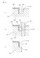
すなわち、MIセンサ素子を製造するに当たっては、多数のMIセンサ素子の基体の母材である基体ウエハに、磁性アモルファスワイヤや検出コイル等の形成を行った後、これを切断して個々のMIセンサ素子を得る(実施例1、図5、図6参照)。ここで、この切断面には、基本的に電極端子等をパターン形成することはない。切断面にパターン形成するということは、切断後に各MIセンサ素子に個別にパターン形成することとなり、生産性の観点から現実的ではないからである。仮に、各MIセンサ素子に個別にパターン形成するとなると、基体ウエハの状態でパターン形成するときに比べて生産性が著しく低下してしまうということとなる。 That is, when manufacturing MI sensor elements, after forming a magnetic amorphous wire, a detection coil, etc. in the base wafer which is a base material of the base of many MI sensor elements, this is cut and individual MI sensors are cut. An element is obtained (see Example 1, FIG. 5 and FIG. 6). Here, the electrode terminals and the like are basically not formed on the cut surface. Forming a pattern on the cut surface is because pattern formation is individually performed on each MI sensor element after cutting, which is not practical from the viewpoint of productivity. If a pattern is individually formed on each MI sensor element, the productivity is significantly reduced as compared with the case where the pattern is formed on the substrate wafer.
上記特許文献1の図8に記載のZ軸用のMIセンサ素子を見ると、切断面である基体の上面に、磁性アモルファスワイヤ及び検出コイルと電気的に接続された電極端子が形成されているように見えるが、実際には、電極端子が形成されている部分は、基体の上面から一段下がった段部となっている(後述の比較例参照)。この段部は当該特許文献における発明の主要部以外の部分であるため、当該図面においては省略してあるだけである。
Looking at the Z-axis MI sensor element described in FIG. 8 of
すなわち、切断する前の基体ウエハの状態において電極端子を一度に形成すべく、基体ウエハには、磁性アモルファスワイヤに直交する基体の辺に対応する位置に溝を形成する。そして、この溝の一部に電極端子を、スパッタやメッキ等を用いて形成する。その後、この溝の一部に形成した電極端子を削らないように、ダイシングソー等によって基体ウエハを切断し、個々のMIセンサ素子を得る。これにより、溝の一部が残って上記段部が形成されることとなる。
そうすると、MIセンサ素子を基体よりも長手方向に突出させることはできないため、その一方の端部は、段部よりも基体の内側に配置されることとなる。それゆえ、少なくとも段部の高さ分、基体の長さよりも磁性アモルファスワイヤの長さを短くせざるを得ず、MIセンサ素子の感度が低下してしまう。
That is, in order to form electrode terminals at once in the state of the substrate wafer before cutting, grooves are formed in the substrate wafer at positions corresponding to the sides of the substrate orthogonal to the magnetic amorphous wires. And an electrode terminal is formed in a part of this groove | channel using sputtering, plating, etc. FIG. Thereafter, the base wafer is cut with a dicing saw or the like so as not to cut the electrode terminal formed in a part of the groove, thereby obtaining individual MI sensor elements. Thereby, a part of groove | channel remains and the said step part is formed.
Then, since the MI sensor element cannot be protruded in the longitudinal direction from the base body, one end portion thereof is disposed inside the base body rather than the stepped portion. Therefore, the length of the magnetic amorphous wire must be made shorter than the length of the substrate by at least the height of the stepped portion, and the sensitivity of the MI sensor element is lowered.
また、上記のような溝を基体に設けると、その溝加工工程が必要となるため、製造コストが高くなると共に、生産性の向上が困難となる。
また、溝を形成するためには基体の強度を確保するために厚みを大きくすることとなり、MIセンサ素子の小型化が困難となる。また、溝加工を行う場合には、その切削加工を容易にすべく、比較的強度の低い材料を基体に用いることとなる。すると、その分、基体の厚みをさらに厚くする必要があり、MIセンサ素子の小型化がさらに難しくなる。
In addition, when the groove as described above is provided in the base body, the groove processing step is required, which increases the manufacturing cost and makes it difficult to improve the productivity.
Further, in order to form the groove, the thickness is increased in order to ensure the strength of the substrate, and it is difficult to reduce the size of the MI sensor element. In addition, when grooving is performed, a material having a relatively low strength is used for the substrate in order to facilitate the cutting process. Accordingly, it is necessary to further increase the thickness of the base, and it becomes more difficult to reduce the size of the MI sensor element.
なお、電極端子を基体における磁性アモルファスワイヤを設けた面と同じ面に形成する場合には、上記のような問題は生じないが、MIセンサ素子の感磁方向をICチップに直交する方向(Z軸方向)とする場合には、当該表面に電極端子を設けることはしない。なぜならば、それらの電極端子には、ICチップ上の電極端子との間で、ワイヤーボンディングを施すなどの処理をする必要があるため、基本的にICチップと電極端子を形成する面とは互いに平行である必要がある。これに対して、基体における磁性アモルファスワイヤを設けた表面と同じ面に電極端子を形成した通常のMIセンサ素子を、単にICチップに直交するように立てると、電極端子を設けた表面はICチップと直交することとなる。そのため、MIセンサ素子の電極端子とICチップの電極端子との間のワイヤーボンディングができない。また、両者をはんだ付けにて接続することも困難である。 In addition, when the electrode terminal is formed on the same surface as the surface on which the magnetic amorphous wire is provided in the base body, the above-mentioned problem does not occur, but the magnetic sensing direction of the MI sensor element is a direction (Z In the case of (axial direction), no electrode terminal is provided on the surface. This is because these electrode terminals need to be subjected to processing such as wire bonding with the electrode terminals on the IC chip, so that the surface on which the IC chip and the electrode terminals are formed is basically Must be parallel. On the other hand, when an ordinary MI sensor element having electrode terminals formed on the same surface as the surface on which the magnetic amorphous wire is provided on the substrate is set so as to be orthogonal to the IC chip, the surface on which the electrode terminals are provided becomes the IC chip. Will be orthogonal. Therefore, wire bonding cannot be performed between the electrode terminal of the MI sensor element and the electrode terminal of the IC chip. It is also difficult to connect the two by soldering.
本発明は、かかる従来の問題点に鑑みてなされたもので、感度が高く、小型化を図ることができるマグネトインピーダンスセンサ素子を提供しようとするものである。 The present invention has been made in view of such conventional problems, and an object of the present invention is to provide a magneto-impedance sensor element that has high sensitivity and can be miniaturized.
本発明は、非磁性体からなる基体と、
該基体上に保持された磁性アモルファスワイヤと、
該磁性アモルファスワイヤが内側を貫通するように形成した被覆絶縁体と、
該被覆絶縁体の周囲に形成した検出コイルと、
上記基体における上記磁性アモルファスワイヤを配置した側の表面から立ち上がる端子搭載面を有する絶縁体からなる端子台と、
上記端子搭載面に形成したワイヤ用電極端子及びコイル用電極端子と、
上記ワイヤ用電極端子と上記磁性アモルファスワイヤに設けた一対のワイヤ通電端とを電気的に接続するワイヤ用接続配線と、
上記コイル用電極端子と上記検出コイルに設けた一対のコイル通電端とを電気的に接続するコイル用接続配線とを有し、
上記端子搭載面は、その法線が上記磁性アモルファスワイヤの長手方向成分を有し、かつ、上記磁性アモルファスワイヤの長手方向における、該磁性アモルファスワイヤの両端の間に配置されていることを特徴とするマグネトインピーダンスセンサ素子にある(請求項1)。
The present invention comprises a substrate made of a non-magnetic material,
A magnetic amorphous wire held on the substrate;
A coated insulator formed so that the magnetic amorphous wire penetrates the inside;
A detection coil formed around the covering insulator;
A terminal block made of an insulator having a terminal mounting surface rising from the surface of the base on which the magnetic amorphous wire is disposed;
An electrode terminal for a wire and an electrode terminal for a coil formed on the terminal mounting surface;
A wire connection wiring for electrically connecting the wire electrode terminal and a pair of wire conduction terminals provided on the magnetic amorphous wire;
A coil connection wiring for electrically connecting the coil electrode terminal and a pair of coil energization ends provided in the detection coil;
The terminal mounting surface has a normal component having a longitudinal component of the magnetic amorphous wire, and is disposed between both ends of the magnetic amorphous wire in the longitudinal direction of the magnetic amorphous wire. In the magneto-impedance sensor element to be (claim 1).
次に、本発明の作用効果につき説明する。
上記マグネトインピーダンスセンサ素子(MIセンサ素子)は、上記端子搭載面を有する上記端子台を備えている。そして、端子搭載面は、上記磁性アモルファスワイヤの長手方向における、該磁性アモルファスワイヤの両端の間に配置されている。これにより、端子台の端子搭載面に、ワイヤ用電極端子及びコイル用電極端子を容易に形成することができると共に、上記磁性アモルファスワイヤの長手方向における上記基体の全体にわたって、磁性アモルファスワイヤを配設することができる。その結果、基体の大きさを大きくすることなく、磁性アモルファスワイヤを長くすることができ、MIセンサ素子の大型化を招くことなく、感度を高くすることができる。
Next, the effects of the present invention will be described.
The magneto-impedance sensor element (MI sensor element) includes the terminal block having the terminal mounting surface. The terminal mounting surface is disposed between both ends of the magnetic amorphous wire in the longitudinal direction of the magnetic amorphous wire. As a result, the electrode terminal for the wire and the electrode terminal for the coil can be easily formed on the terminal mounting surface of the terminal block, and the magnetic amorphous wire is arranged over the entire base in the longitudinal direction of the magnetic amorphous wire. can do. As a result, the magnetic amorphous wire can be lengthened without increasing the size of the substrate, and the sensitivity can be increased without increasing the size of the MI sensor element.
すなわち、上述したごとく、MIセンサ素子を製造するにあたっては、一般には、多数のMIセンサ素子の基体の母材である基体ウエハに、磁性アモルファスワイヤや検出コイル等の形成を行った後、これを切断して個々のMIセンサ素子を得る。このとき、MIセンサ素子が上記端子台を有していれば、個々のMIセンサ素子に切断する前の状態において、ワイヤ用電極端子及びコイル用電極端子を容易に形成することができる。 That is, as described above, in manufacturing an MI sensor element, generally, after forming a magnetic amorphous wire, a detection coil, etc. on a base wafer which is a base material of a base of a large number of MI sensor elements, this is used. Cut to obtain individual MI sensor elements. At this time, if the MI sensor element has the terminal block, the wire electrode terminal and the coil electrode terminal can be easily formed in a state before being cut into individual MI sensor elements.
また、MIセンサ素子が端子台を有していることにより、上述した溝(段部)を基体ウエハに形成する必要もない。そのため、段部を形成した分、磁性アモルファスワイヤの長さを短くせざるを得ないという問題は生じず、基体の大きさに対して磁性アモルファスワイヤの長さが短くなってしまうという不具合を招くことがない。それゆえ、磁性アモルファスワイヤの長さをMIセンサ素子全体の長さと同等とすることも可能となり、MIセンサ素子の小型化と高感度化との両立が可能となる。 Further, since the MI sensor element has the terminal block, it is not necessary to form the above-described groove (step) in the base wafer. Therefore, there is no problem that the length of the magnetic amorphous wire has to be shortened by the amount of the stepped portion, and the length of the magnetic amorphous wire is shortened with respect to the size of the base. There is nothing. Therefore, it is possible to make the length of the magnetic amorphous wire equal to the entire length of the MI sensor element, and it is possible to achieve both miniaturization and high sensitivity of the MI sensor element.
また、上記のような溝加工工程が不要となるため、製造コストを低減できると共に、生産性の向上を図ることができる。
また、溝を形成する必要がないため基体の厚みを特に大きくする必要がなく、MIセンサ素子の小型化が容易となる。また、切削加工の容易化も特に考慮する必要がなくなるため、強度の高い材料を基体に用いることもでき、その分、基体の厚みをさらに小さくすることもでき、MIセンサ素子の小型化がさらに容易となる。
Further, since the groove processing step as described above is not necessary, the manufacturing cost can be reduced and the productivity can be improved.
In addition, since it is not necessary to form a groove, it is not necessary to increase the thickness of the substrate, and the MI sensor element can be easily downsized. In addition, since it is not necessary to take into account the ease of cutting, it is possible to use a material with high strength for the base, and accordingly, the thickness of the base can be further reduced, further reducing the size of the MI sensor element. It becomes easy.
以上のごとく、本発明によれば、感度が高く、小型化を図ることができるマグネトインピーダンスセンサ素子を提供することができる。 As described above, according to the present invention, it is possible to provide a magneto-impedance sensor element that has high sensitivity and can be miniaturized.
本発明(請求項1)において、上記端子搭載面は、その法線が上記磁性アモルファスワイヤの長手方向となるように形成されていることが好ましい(請求項2)。
この場合には、MIセンサ素子をICチップ等に実装するにあたり、磁性アモルファスワイヤがICチップの主面に直交するように配置する際、ワイヤ用電極端子及びコイル用電極端子をICチップの主面と平行にすることができる。その結果、ワイヤ用電極端子及びコイル用電極端子と、ICチップとの間のワイヤボンディング等、電気的接続を容易に行うことができる。
In the present invention (Claim 1), it is preferable that the terminal mounting surface is formed such that a normal line thereof is in a longitudinal direction of the magnetic amorphous wire (Claim 2).
In this case, when the MI sensor element is mounted on the IC chip or the like, when the magnetic amorphous wire is arranged so as to be orthogonal to the main surface of the IC chip, the wire electrode terminal and the coil electrode terminal are arranged on the main surface of the IC chip. And can be parallel. As a result, electrical connection such as wire bonding between the wire electrode terminal and the coil electrode terminal and the IC chip can be easily performed.
また、上記端子台は、上記磁性アモルファスワイヤ、被覆絶縁体、及び検出コイルの形成領域以外の領域に形成されていることが好ましい(請求項3)。
この場合には、上記端子台が上記磁性アモルファスワイヤ、被覆絶縁体、及び検出コイルを覆うことがないため、磁性アモルファスワイヤへかかる応力や、磁性アモルファスワイヤへの結露等を防ぎ、正確な磁界検出を確保することができる。
The terminal block is preferably formed in a region other than the formation region of the magnetic amorphous wire, the covering insulator, and the detection coil.
In this case, since the terminal block does not cover the magnetic amorphous wire, the covering insulator, and the detection coil, stress applied to the magnetic amorphous wire, dew condensation on the magnetic amorphous wire, etc. can be prevented and accurate magnetic field detection can be performed. Can be secured.
仮に磁性アモルファスワイヤを覆うように端子台が配設されると、磁性アモルファスワイヤに応力がかかるおそれがあるし、磁性アモルファスワイヤと端子台との間に存在する空気の結露等による寄生容量の変化が生じるおそれがある。そして、この応力や寄生容量の変化に起因して、磁性アモルファスワイヤに供給される電流が変動してしまい、MIセンサ素子の磁気感度(出力/印加磁場)のバラツキ(例えば磁気感度に対して約10%のバラツキ)が生じるおそれがある。そのため、磁性アモルファスワイヤを覆わないように端子台を設けることにより、かかる不具合を回避することができる。すなわち、MIセンサ素子の磁気感度のバラツキをほとんどなくす(例えば磁気感度に対して1%未満のバラツキとする)ことができる。 If the terminal block is placed so as to cover the magnetic amorphous wire, the magnetic amorphous wire may be stressed, and the parasitic capacitance changes due to condensation of air existing between the magnetic amorphous wire and the terminal block. May occur. Due to this change in stress and parasitic capacitance, the current supplied to the magnetic amorphous wire fluctuates, and variations in the magnetic sensitivity (output / applied magnetic field) of the MI sensor element (for example, about the magnetic sensitivity). 10% variation) may occur. Therefore, such a problem can be avoided by providing the terminal block so as not to cover the magnetic amorphous wire. That is, the variation in the magnetic sensitivity of the MI sensor element can be almost eliminated (for example, the variation is less than 1% with respect to the magnetic sensitivity).
また、上述した応力の問題や寄生容量の問題を解決するために、端子台を構成する絶縁材料の線膨張係数、接着力、誘電率等を適切な値にすることも考えられるが、その場合には材料選択の自由が著しく制限されてしまうという問題がある。かかる問題も、請求項3の発明によれば解決することができる。
In addition, in order to solve the above-mentioned stress problem and parasitic capacitance problem, it is possible to set the linear expansion coefficient, adhesive force, dielectric constant, etc. of the insulating material constituting the terminal block to appropriate values. However, there is a problem that freedom of material selection is significantly limited. Such a problem can also be solved by the invention of
また、電子回路を形成してなるICチップに、該ICチップの主面の法線方向に上記磁性アモルファスワイヤの長手方向が向くように実装するための素子であることが好ましい(請求項4)。
この場合には、仮に上記ワイヤ用電極端子及びコイル用電極端子の法線が上記磁性アモルファスワイヤの長手方向成分を有していないと、ICチップの主面に形成された電子回路の端子との接続が困難である。それゆえ、基体における磁性アモルファスワイヤを形成した表面に上記ワイヤ用電極端子及びコイル用電極端子を設けることは望ましくなく、上記表面に対して角度をもった面、より好ましくは直交する面にワイヤ用電極端子及びコイル用電極端子を形成する。
そこで、このようなMIセンサ素子において、本発明を適用することにより、その作用効果を充分に発揮させることができる。
Further, it is preferably an element for mounting on an IC chip formed with an electronic circuit so that the longitudinal direction of the magnetic amorphous wire is oriented in the normal direction of the main surface of the IC chip. .
In this case, if the normal line of the wire electrode terminal and the coil electrode terminal does not have the longitudinal component of the magnetic amorphous wire, the wire terminal and the terminal of the electronic circuit formed on the main surface of the IC chip Connection is difficult. Therefore, it is not desirable to provide the wire electrode terminal and the coil electrode terminal on the surface of the substrate on which the magnetic amorphous wire is formed, and for the wire on the surface having an angle with respect to the surface, more preferably the surface orthogonal to the surface. An electrode terminal and a coil electrode terminal are formed.
Therefore, by applying the present invention to such an MI sensor element, the function and effect can be sufficiently exhibited.
なお、ここで、MIセンサ素子のICチップへの実装とは、MIセンサ素子をワイヤーボンディング等によって上記ICチップに直接電気的接続することの他、例えば、ICチップを搭載したIC基板を介してMIセンサ素子を間接的に電気的接続することをも含む。 Here, the mounting of the MI sensor element on the IC chip means that the MI sensor element is directly electrically connected to the IC chip by wire bonding or the like, for example, via an IC substrate on which the IC chip is mounted. It also includes indirectly connecting the MI sensor elements.
また、電子回路を形成してなるICチップを搭載したIC基板に、該IC基板の主面の法線方向に上記磁性アモルファスワイヤの長手方向が向くように実装するための素子であってもよい(請求項5)。
ICチップを搭載したIC基板を介してMIセンサ素子を間接的に電気的接続するような場合には、上記のごとく該IC基板の主面の法線方向に上記磁性アモルファスワイヤの長手方向が向くようにMIセンサ素子を実装することにより、IC基板の主面に形成された電子回路の端子と上記ワイヤ用電極端子及びコイル用電極端子との接続が容易となる。そしてそのような構成において、本発明の作用効果が充分に発揮できる。
Further, it may be an element for mounting on an IC substrate on which an IC chip formed with an electronic circuit is mounted so that the longitudinal direction of the magnetic amorphous wire is oriented in the normal direction of the main surface of the IC substrate. (Claim 5).
When the MI sensor element is indirectly electrically connected via an IC substrate on which an IC chip is mounted, the longitudinal direction of the magnetic amorphous wire is oriented in the normal direction of the main surface of the IC substrate as described above. By mounting the MI sensor element in this manner, it is easy to connect the terminals of the electronic circuit formed on the main surface of the IC substrate with the wire electrode terminals and the coil electrode terminals. And in such a structure, the effect of this invention can fully be exhibited.
(実施例1)
本発明の実施例にかかるマグネトインピーダンスセンサ素子につき、図1〜図6を用いて説明する。
本例のマグネトインピーダンスセンサ素子(MIセンサ素子)1は、図1〜図3に示すごとく、非磁性体からなる基体2と、該基体2上に保持された磁性アモルファスワイヤ3と、該磁性アモルファスワイヤ3が内側を貫通するように形成した被覆絶縁体4と、該被覆絶縁体4の周囲に形成した検出コイル5とを有する。
Example 1
A magneto-impedance sensor element according to an embodiment of the present invention will be described with reference to FIGS.
As shown in FIGS. 1 to 3, a magneto-impedance sensor element (MI sensor element) 1 of this example includes a
基体2における磁性アモルファスワイヤ3を配置した側の表面21には、該表面21から立ち上がる端子搭載面61を有する絶縁体からなる端子台6が設けてある。
端子搭載面61には、一対のワイヤ用電極端子11及び一対のコイル用電極端子12が形成されている。ただし、一対のワイヤ用電極端子11のうちの一方と一対のコイル用電極端子12の一方とが一つの電極を基準電位として共有するようにすることもできる。この場合、ワイヤ用電極端子11及びコイル用電極端子12の合計数を3個とすることができる。
A
On the
ワイヤ用電極端子11と磁性アモルファスワイヤ3に設けた一対のワイヤ通電端31とは、ワイヤ用接続配線110によって電気的に接続されている。
コイル用電極端子12と検出コイル5に設けた一対のコイル通電端51とは、コイル用接続配線120によって電気的に接続されている。
端子搭載面61は、その法線が磁性アモルファスワイヤ3の長手方向成分を有し、かつ、磁性アモルファスワイヤ3の長手方向における、磁性アモルファスワイヤ3の両端311、311の間に配置されている。
The
The
The
本例においては、端子搭載面61は、その法線が磁性アモルファスワイヤ3の長手方向となるように形成されている。
また、図1、図3に示すごとく、端子台6は、磁性アモルファスワイヤ3、被覆絶縁体4、及び検出コイル5の形成領域以外の領域に形成されている。すなわち、端子台6は、ワイヤ用接続配線110及びコイル用接続配線120の一部を覆うように、基体2の表面に形成されているが、磁性アモルファスワイヤ3、被覆絶縁体4、及び検出コイル5を覆わないように、これらの形成領域とは外れた位置において形成されている。
In this example, the
As shown in FIGS. 1 and 3, the
本例のMIセンサ素子1は、図4に示すごとく、電子回路を形成してなるICチップ7に、該ICチップ7の主面71の法線方向に磁性アモルファスワイヤ3の長手方向が向くように実装するための素子である。
MIセンサ素子1において、ICチップ7に実装したときICチップ7の主面71に直交する方向となる方向をZ軸方向という。すなわち磁性アモルファスワイヤ3の長手方向と一致する方向がZ軸方向である。
In the
In the
基体2としては、例えば、絶縁性のアルミナ系セラミックス、半導体のシリコンウェハ、導体の金属などが使用でき、表面21に直交する方向の厚さは、例えば、0.1mm〜0.5mmとすることができる。本例においては、上記厚さは0.3mmとした。また、基体2のZ軸方向の高さは0.6mmとした。
磁性アモルファスワイヤ3は、零磁歪アモルファスのCoFeSiB系合金からなり、例えば、直径20μm以下とすることができる。ここでは、直径を10μmとした。そして、この磁性アモルファスワイヤ3は、図1に示すごとく、基体2の表面21に、基体2のZ軸方向の全体にわたって配設されている。本例では、この磁性アモルファスワイヤ3の長さは0.6mmとした。
As the
The magnetic
この磁性アモルファスワイヤ3の両端におけるワイヤ通電端31は、基体2の表面21に形成された通電パッド310に電気的に接続されている。
また、磁性アモルファスワイヤ3の一対の通電端31の間の部分は、被覆絶縁体4によって被覆されている。被覆絶縁体4は、例えば、酸化アルミニウム、酸化ケイ素などの無機質の絶縁材料やエポキシ系樹脂などの有機質の絶縁材料を用いて構成することができる。
Wire energization ends 31 at both ends of the magnetic
Further, the portion between the pair of energization ends 31 of the magnetic
そして、被覆絶縁体4の外周面に、検出コイル5が形成されている。検出コイル5は、基体2の表面21に成膜された平面パターン501と、被覆絶縁体4の外表面に成膜された立体パターン502とが適宜接続されることによって、被覆絶縁体4の外周を螺旋状に巻回するように配設されている。そして、検出コイル5の巻回パターンの両端がコイル通電端51である。ここで、検出コイル5の巻数は15ターンである。
A
本例においては、基体2の表面21から盛り上がるように、磁性アモルファスワイヤ3、被覆絶縁体4、検出コイル5を配設しているが、特許文献1の図2に開示されているように、基体に溝を形成し、その溝の中に磁性アモルファスワイヤ、被覆絶縁体、検出コイルを配置してもよい。ただし、このような溝を形成すると、基体を厚くする必要があるため、小型化の観点からは、本例の構造を採用することが望ましい。
In this example, the magnetic
一対のコイル通電端51には、基体2の表面21に形成されたコイル用接続配線120の一端が接続されている。また、一対のワイヤ通電端31には、通電パッド310を介して、基体2の表面21に形成されたワイヤ用接続配線110の一端が接続されている。
ワイヤ用接続配線110の他端は、ワイヤ用電極端子11に接続され、コイル用接続配線120の他端は、コイル用電極端子12に接続されている。
One end of a
The other end of the
また、基体2の表面21に設けられた端子台6は、エポキシ系樹脂やセラミック等の絶縁体からなり、ワイヤ用接続配線110及びコイル用接続配線120を覆うように形成されている。そして、端子台6は、基体2のZ軸方向における一端(上端22)から、充分に内側に後退した位置(例えば150〜550μm後退した位置)に、Z軸に直交する平坦面である端子搭載面61を設けてなる。ここでは、端子搭載面61を上端22から200μm後退させている。
この端子搭載面61に、上記一対のワイヤ用電極端子11及び一対のコイル用電極端子12を設けている。
The
The pair of
本例においては、端子台6は、磁性アモルファスワイヤ3、被覆絶縁体4、及び検出コイル5の形成領域、及び端子搭載面61から該端子搭載面61が向いた方向における基体2の端面(上端22)までの領域を除いて、基体2の表面21の全面に形成されている。
また、端子台6の厚み、すなわち端子搭載面61の幅は、例えば80〜150μmである。ここでは、端子搭載面61の幅を100μmとした。
In this example, the
Moreover, the thickness of the
ワイヤ用接続配線110におけるワイヤ用電極端子11側の端子部111は、端子搭載面61から一部がはみ出すように形成され、ワイヤ用電極端子11と接続されている。同様に、コイル用接続配線120におけるコイル用電極端子12側の端子部121も、端子搭載面61から一部がはみ出すように形成され、コイル用電極端子12と接続されている。
A
また、図4に示すごとく、MIセンサ素子1は、いわゆるZ軸用としてICチップ7に実装され、磁性アモルファスワイヤ3の長手方向がICチップ7の主面71に直交するように配設されている。ICチップ7は、マザーボードとICチップ7とを接続するためのIC基板73に搭載されており、IC基板73の主面731とICチップ7の主面71とは互いに平行となっている。MIセンサ素子1は、ICチップ7の脇において、IC基板73の主面731に搭載されている。
As shown in FIG. 4, the
そして、MIセンサ素子1におけるワイヤ用電極端子11及びコイル用電極端子12は、それぞれ、ICチップ7の主面71に形成された電子回路における所定の端子、又はIC基板73の主面731に形成された電子回路における所定の端子に、ボンディングワイヤ72にて電気的に接続される。具体的には、MIセンサ素子1におけるコイル用電極端子12は、2本ともICチップ7の端子にボンディング接続されているが、ワイヤ用電極端子11は、一方がICチップ7の端子に、他方がIC基板73の端子にそれぞれボンディング接続されている。
なお、この接続の仕方は、一例であって、例えばMIセンサ素子1におけるワイヤ用電極端子11及びコイル用電極端子12のすべてをICチップ7の端子に接続してもよいし、IC基板73の端子に接続してもよい。
The
This connection method is an example. For example, all of the
また、ICチップ7には、該ICチップ7の主面71に平行であると共に互いに直交する方向に磁性アモルファスワイヤ30を備えた、X軸用のMIセンサ素子10及びY軸用のMIセンサ素子100が、実装される。X軸用のMIセンサ素子10及びY軸用のMIセンサ素子100は、本例のZ軸用のMIセンサ素子1と略同様の構成要素を有するが、端子台6がなく、ワイヤ用電極端子11及びコイル用電極端子12が、基体2における磁性アモルファスワイヤ30を設けた面と同じ表面に形成されている点において、Z軸用のMIセンサ素子1と異なる。
In addition, the
このように、本例のMIセンサ素子1を含めた3個のMIセンサ素子(1、10、100)によって、地磁気を利用して3次元的な方位を検出する磁気方位センサ70を構成している。かかる地磁気方位センサ70は、携帯電話機等の携帯端末機器などに搭載することができる。
なお、ここでは、本例のZ軸用のMIセンサ素子1を、X軸用及びY軸用のMIセンサ素子10、100と組み合わせて、3軸の磁気方位センサ70としたが、本例のMIセンサ素子1を含む2つのMIセンサ素子によって2軸の磁気方位センサを構成することもできる。
また、本例のMIセンサ素子1は、このような磁気方位センサに限らず、例えば、電流センサ等に用いることもできる。この場合には、本例のMIセンサ素子1を一つだけ用いてセンサを構成することもできる。
As described above, the three MI sensor elements (1, 10, 100) including the
Here, the Z-axis
Further, the
本例のMIセンサ素子1を製造するに当たっては、図5に示すごとく、多数のMIセンサ素子1の基体2の母材である基体ウエハ20に、磁性アモルファスワイヤ3や検出コイル5等の形成を行う。すなわち、例えば10cm四方程度の大きい基体ウエハ20上において、多数のMIセンサ素子1(例えば1mm四方以下の大きさ)のパターニングを一度に行う。
このとき、基体2の表面21には、端子台6の形成も行う。端子台6を形成するに当たっては、例えば感光性のエポキシ樹脂を用いることができる。すなわち、基体2の表面21の全体に樹脂を塗布した後、乾燥させ、次いで、端子台6を形成したい部分のみに光が当たるようにマスキングした状態で樹脂を露光する。次いで、現像液にて現像することにより、所定の位置に所定の大きさ、形状の端子台6を形成する。
In manufacturing the
At this time, the
また、端子台6の端子搭載面61に、スパッタリング及びメッキを用いて、ワイヤ用電極端子11及びコイル用電極端子12を成膜する。
端子台6、ワイヤ用電極端子11及びコイル用電極端子12以外の形成方法については、省略したが、MIセンサ素子1のすべての要素を形成した後、図6に示すごとく、基体ウエハ20を、ダイシングソーを用いて切断し、個々のMIセンサ素子1を得る。このとき、ダイシングソーの切り代201(例えば200μm)を考慮して、切断面がMIセンサ素子1の所望の輪郭となるようにする。
Further, the
The forming method other than the
次に、本例の作用効果につき説明する。
上記マグネトインピーダンスセンサ素子1は、端子搭載面61を有する端子台6を備え、端子搭載面61は、磁性アモルファスワイヤ3の長手方向における、磁性アモルファスワイヤ3の両端311、311の間に配置されている。これにより、端子台6の端子搭載面61に、ワイヤ用電極端子11及びコイル用電極端子12を容易に形成することができると共に、磁性アモルファスワイヤ3の長手方向における基体2の全体にわたって、磁性アモルファスワイヤ3を配設することができる。その結果、基体2の大きさを大きくすることなく、磁性アモルファスワイヤ3を長くすることができ、MIセンサ素子1の大型化を招くことなく、感度を高くすることができる。
Next, the function and effect of this example will be described.
The magneto-
すなわち、上述したごとく、MIセンサ素子1を製造するにあたっては、一般には、基体ウエハ20に、磁性アモルファスワイヤ3や検出コイル5等の形成を行った後、これを切断して個々のMIセンサ素子1を得る。このとき、MIセンサ素子1が端子台6を有していることにより、個々のMIセンサ素子1に切断する前の状態において、ワイヤ用電極端子11及びコイル用電極端子12を容易に形成することができる。
That is, as described above, in manufacturing the
また、MIセンサ素子1が端子台6を有していることにより、比較例に示す溝(図14(A)の符号99参照)を基体ウエハ20に形成する必要もない。そのため、磁性アモルファスワイヤ3の長さをMIセンサ素子1全体の長さと同等とすることも可能となり、MIセンサ素子1の小型化と高感度化との両立が可能となる。
Further, since the
また、溝加工工程が不要となるため、製造コストを低減できると共に、生産性の向上を図ることができる。
また、溝を形成する必要がないため基体2の厚みを特に大きくする必要がなく、MIセンサ素子1の小型化が容易となる。また、切削加工の容易化も特に考慮する必要がなくなるため、強度の高い材料を基体2に用いることもでき、その分、基体2の厚みをさらに小さくすることもでき、MIセンサ素子1の小型化がさらに容易となる。
Further, since the grooving process is not required, the manufacturing cost can be reduced and the productivity can be improved.
Further, since it is not necessary to form a groove, it is not necessary to increase the thickness of the
また、端子台6は、磁性アモルファスワイヤ3、被覆絶縁体4、及び検出コイル5の形成領域以外の領域に形成されている。これにより、端子台6が磁性アモルファスワイヤ3、被覆絶縁体4、及び検出コイル5を覆うことがないため、磁性アモルファスワイヤ3へ応力がかかることを防ぎ、正確な磁界検出を確保することができる。
The
以上のごとく、本例によれば、感度が高く、小型化を図ることができるマグネトインピーダンスセンサ素子を提供することができる。 As described above, according to this example, it is possible to provide a magneto-impedance sensor element that has high sensitivity and can be miniaturized.
以下においては、図7、図8を用いて、実施例1のMIセンサ素子1について行った特性評価につき説明する。
すなわち、MIセンサ素子1を図7に示す電子回路8に組み込み、以下のような磁気センシング評価を行った。
上記電子回路8は、MIセンサ素子1の磁性アモルファスワイヤ3に入力するためのパルス信号を発振するパルス発振回路81と、MIセンサ素子1の検出コイル5において生じた検出電圧を信号処理するための信号処理回路82とを有する。信号処理回路82は、検出コイル5と出力端子83との間のスイッチングを行うアナログスイッチ821と、パルス信号に連動してアナログスイッチ821のオンオフを行うサンプルタイミング調整回路822と、検出コイル5において生じた誘起電圧を増幅する増幅器823とを有する。
Hereinafter, characteristic evaluation performed on the
That is, the
The electronic circuit 8 performs signal processing on a
パルス発振回路81は、主として200MHzを含む170mAの強さであって、信号間隔が1μsecのパルス信号を生成し、このパルス信号を磁性アモルファスワイヤ3に入力する。このパルス電流は、定常値の90%から10%に立ち下がる遮断時間を4ナノ秒とした。これにより、パルス信号の立ち下り時に、MIセンサ素子1の検出コイル5に、磁性アモルファスワイヤ3の長手方向(Z軸方向)の磁界に応じた誘起電圧が生じる。この誘起電圧を、アナログスイッチ821を介して増幅器823によって増幅し、出力端子83から出力する。
The
このような電子回路8を用いて、MIセンサ素子1を、水平軸を中心にして360°回転させながら、その出力特性を評価する。
まず、MIセンサ素子1の磁性アモルファスワイヤ3の長手方向(Z軸方向)が鉛直方向を向いた状態を、回転角度0°とし、このときのMIセンサ素子1の出力信号の大きさを0mVとする。そして、このMIセンサ素子1を、水平軸を中心に360°回転させた。このときの出力信号の変化を図8に示す。
Using such an electronic circuit 8, the output characteristics of the
First, the state in which the longitudinal direction (Z-axis direction) of the magnetic
同図から分かるように、出力信号は、きれいなサインカーブを描き、精度よく地磁気のZ軸方向の成分を検出していることが分かる。これにより、実施例1におけるMIセンサ素子1は、小型化しても、充分な検出精度を確保することができることが分かる。
As can be seen from the figure, the output signal draws a beautiful sine curve and accurately detects the component of the geomagnetism in the Z-axis direction. Thus, it can be seen that the
(実施例2)
本例は、図9、図10に示すごとく、実施例1に比べて端子台6の大きさを小さくした例である。
すなわち、端子台6のZ軸方向の高さを短くしている。具体的には、実施例1のMIセンサ素子1における端子台6の高さ0.4mmに対して、本例のMIセンサ素子1における端子台6の高さは0.13mmとした。
その他は、実施例1と同様である。
(Example 2)
In this example, as shown in FIGS. 9 and 10, the size of the
That is, the height of the
Others are the same as in the first embodiment.
端子台6としては、ワイヤ用電極端子11及びコイル用電極端子12を搭載する端子搭載面61を充分に確保できれば、本発明の効果を充分に得ることができる。そのため、実施例1のように、基体2の表面21において大きな領域に形成する必要は必ずしもなく、基体2との密着性が損なわれなければ、端子台6は、端子搭載面61の面積を充分に維持しつつ、種々の形態をとることが考えられる。
As the
すなわち、上記以外にも、たとえば、ワイヤ用電極端子11及びコイル用電極端子12のそれぞれに対応するように個別に分割して形成した端子台としてもよいし、階段状に形成した端子台としてもよい。
That is, in addition to the above, for example, it may be a terminal block formed by being individually divided so as to correspond to each of the electrode terminal for
(比較例)
本例は、図11〜図13に示すごとく、実施例1、2において示した端子台6を設けることなく、基体92に直接、ワイヤ用電極端子11及びコイル用電極端子12を設けたマグネトインピーダンスセンサ素子9の例である。
本例のMIセンサ素子9は、実施例1、2と同様に、基体92の表面921に磁性アモルファスワイヤ93、被覆絶縁体4、検出コイル5、ワイヤ用接続配線110、コイル用接続配線120を形成してなる。そして、基体92における磁性アモルファスワイヤ93の長手方向(Z軸方向)の一端に段部96を有し、そのZ軸方向に直交する面に、ワイヤ用電極端子11及びコイル用電極端子12を設けてなる。
上記段部96は、基体92におけるZ軸方向及び厚み方向に直交する方向(図11の左右方向)の全体にわたって形成されている。
なお、磁性アモルファスワイヤ93、被覆絶縁体4、及び検出コイル5からなる構成体の構成は、実施例1と同様であって、その大きさや検出コイル5の巻数等も同様である。
(Comparative example)
In this example, as shown in FIGS. 11 to 13, the magneto-impedance in which the
In the MI sensor element 9 of this example, the magnetic
The
In addition, the structure of the structure which consists of the magnetic
かかる段部96は、磁性アモルファスワイヤ3と直交する面にワイヤ用電極端子11及びコイル用電極端子12を形成する必要のある、いわゆるZ軸用のMIセンサ素子9において、製造上の観点から必然的に形成されるものである。
すなわち、かかるMIセンサ素子9を製造するに当たっては、上述したごとく、多数のMIセンサ素子9の基体92の母材である基体ウエハ920に、多数のMIセンサ素子9のパターニングを一度に行った後、図14(B)に示すごとく、基体ウエハ920をダイシングソー98によって切断して、個々のMIセンサ素子9に切り分ける。
Such a
That is, in manufacturing the MI sensor element 9, as described above, after patterning a large number of MI sensor elements 9 on the
ここで、切断される前の基体ウエハ920の表面には、後に切断する切断線に沿って溝99が形成されている。すなわち、基体ウエハ920の状態で、図14(A)に示すごとく、例えば深さ200μm、幅200μmの溝99を形成しておく。その後、溝99の内側面991及びこれに連続する基体92の表面921に、ワイヤ用電極端子11及びコイル用電極端子12のパターニングを行う。そして、ダイシングソー98による切断を、溝99の内側面991よりも若干(例えば70μm)外側において行う。これにより、切断前の状態で、溝99の内側面991にワイヤ用電極端子11及びコイル用電極端子12のパターニングを行うことができる。
そして、図14(C)に示すごとく、切断後には、この溝99の一部分が上記段部96として残ることとなる。
Here, a
And as shown in FIG.14 (C), after cutting | disconnection, a part of this groove |
上記のごとく溝加工を行った後に基体ウエハ920の切断を行うのは、ワイヤ用電極端子11及びコイル用電極端子12の形成が終わるまで、基体ウエハ920の一体性を保つためである。
すなわち、上記のようなZ軸用のMIセンサ素子9は、上記のごとく、磁性アモルファスワイヤ93と直交する面にワイヤ用電極端子11及びコイル用電極端子12を形成する必要があるため、上記基体92の表面921と直交する面を、基体92に形成する必要がある。それゆえ、溝加工を行わないと、基体ウエハ920の状態のままでワイヤ用電極端子11及びコイル用電極端子12のパターニングを行うことができない。溝加工を行わない場合、切り離された基体2の一つ一つに対して個別に電極端子の形成を行わねばならず、生産性が著しく低下する。それゆえ、溝加工を行うことにより、基体ウエハ920の一体性を保ったまま、電極端子の形成が行えるようにしている。
The reason why the
That is, since the Z-axis MI sensor element 9 as described above needs to form the
ところが、溝99の一部分として残る上記段部96が基体92のZ軸方向の一端の全体にわたって存在することにより、図11に示すごとく、磁性アモルファスワイヤ93の長さを、基体92のZ軸方向長さよりも短くせざるを得ない。例えば、基体92の上端922と段部96との段差が70μmであれば、磁性アモルファスワイヤ93を基体92よりも70μm以上短くすることとなる。さらに、図12に示すごとく、ワイヤ用電極端子11及びコイル用電極端子12に接続されるボンディングワイヤ72の高さを考慮すると、ボンディングワイヤ72を含めたMIセンサ素子9のZ軸方向の占有高さH(図12)に対して、磁性アモルファスワイヤ93の長さL(図11)が大きく下回ることとなる。
However, since the
また、上記のように、ワイヤ用電極端子11及びコイル用電極端子12を配置するために段部96を基体92に形成するには、溝加工を行う必要がある。そうすると、製造コストが高くなると共に、基体92の強度を確保すべく厚みを厚くする必要がある。また、基体92に溝加工することを考えると、加工容易な材料を基体92として選定する必要があるが、かかる材料は、機械的強度がどうしても低いため、さらに基体92の厚みを大きくする必要が生じる。
その結果、MIセンサ素子9の厚みも大きくなることとなる。
このように、本例のMIセンサ素子9は、磁性アモルファスワイヤ3の長さを長くしつつ、小型化を図ることが困難である。
Further, as described above, in order to form the stepped
As a result, the thickness of the MI sensor element 9 is also increased.
Thus, it is difficult to reduce the size of the MI sensor element 9 of this example while increasing the length of the magnetic
これに対して、上述のごとく、本発明のMIセンサ素子1(実施例1、3)は、図1、図9に示すごとく、磁性アモルファスワイヤ3の長さを、基体2のZ軸方向の長さと同等まで長くすることが可能となるため、磁性アモルファスワイヤ3の長さを長くしつつ、MIセンサ素子1の小型化を図ることができる。
また、本発明のMIセンサ素子1は、上記のような溝加工の必要もないため、基体2の厚みを大きくする必要もなく、さらなる小型化を可能とする。
On the other hand, as described above, the MI sensor element 1 (Examples 1 and 3) of the present invention has the length of the magnetic
Further, since the
また、端子台6における端子搭載面61の位置も自由に設定することができるため、端子搭載面61と、基体2のZ軸方向の上端との間の距離を充分に大きくすることもできる。これにより、図2に示すごとく、ワイヤ用電極端子11及びコイル用電極端子12にボンディングワイヤ72を接続しても、ボンディングワイヤ72の上端を基体2の上端から突出しないようにすることもできる。それゆえ、ボンディングワイヤ72を含めたMIセンサ素子1の占有高さに対しても、磁性アモルファスワイヤ3の長さが短くなることを防ぐことができる。
Moreover, since the position of the
ここで、ボンディングワイヤを含めたMIセンサ素子のZ軸方向の占有高さHと、磁性アモルファスワイヤの長さLとの比(H/L)を、MIセンサ素子の小型化指標φとして、実施例1のMIセンサ素子1と、比較例のMIセンサ素子9とを比較した。小型化指標φが小さいほど(1に近づくほど)同等の性能での小型化が達成されていることとなる。
Here, the ratio (H / L) between the height H occupied in the Z-axis direction of the MI sensor element including the bonding wire and the length L of the magnetic amorphous wire is used as the miniaturization index φ of the MI sensor element. The
まず、比較例のMIセンサ素子9の小型化指標φを算出する。
比較例のMIセンサ素子9の基体92のZ軸方向の下端923から段部96までの高さは0.6mmで、段部96から上端922までの高さが0.07mmである。また、段部96からのボンディングワイヤ72のZ軸方向高さは0.15mmである。それゆえ、比較例のMIセンサ素子の占有高さH(図12)は、H=0.6mm+0.15mm=0.75mmである。
したがって、比較例のMIセンサ素子の小型化指標φは、φ=0.75mm/0.6mm=1.25となる。
First, the miniaturization index φ of the MI sensor element 9 of the comparative example is calculated.
The height from the
Therefore, the miniaturization index φ of the MI sensor element of the comparative example is φ = 0.75 mm / 0.6 mm = 1.25.
一方、実施例1のMIセンサ素子1は、図2に示すごとく、ボンディングワイヤ72が基体2の上端22よりも下方に位置するため、ボンディングワイヤを含めても、そのZ軸方向の占有高さH(図1)は、基体2のZ軸方向高さに一致し、0.6mmである。そして、磁性アモルファスワイヤ3は、基体2のZ軸方向の全長にわたって形成されているため、その長さLも0.6mmである。
On the other hand, as shown in FIG. 2, the
したがって、実施例1のMIセンサ素子の小型化指標φは、φ=0.6mm/0.6mm=1となる。
すなわち、実施例1のMIセンサ素子は、比較例のMIセンサ素子に対して、Z軸方向に20%の小型化を実現している。つまり、同じ磁性アモルファスワイヤの長さ、すなわち同じ磁気感度を確保しつつ、Z軸方向の小型化を20%実現することができる。
Therefore, the miniaturization index φ of the MI sensor element of Example 1 is φ = 0.6 mm / 0.6 mm = 1.
That is, the MI sensor element of Example 1 is 20% smaller in the Z-axis direction than the MI sensor element of the comparative example. That is, it is possible to achieve 20% reduction in size in the Z-axis direction while ensuring the same magnetic amorphous wire length, that is, the same magnetic sensitivity.
なお、ボンディングワイヤ以外の接続方法(例えば半田接続)を採用する場合などには、ボンディングワイヤの高さを考慮する必要がないが、この場合でも、実施例1のMIセンサ素子1は、比較例のMIセンサ素子9よりも小型となる。
すなわち、この場合、比較例のMIセンサ素子9の小型化指標φは、φ=0.67mm/0.6mm≒1.12となり、実施例1のMIセンサ素子1の小型化指標φは、φ=0.6mm/0.6mm=1となる。それゆえ、この場合でも、約10%の小型化を実現することができる。
It should be noted that when a connection method other than the bonding wire (for example, solder connection) is adopted, it is not necessary to consider the height of the bonding wire, but even in this case, the
That is, in this case, the miniaturization index φ of the MI sensor element 9 of the comparative example is φ = 0.67 mm / 0.6 mm≈1.12, and the miniaturization index φ of the
また、比較例のMIセンサ素子9は、上記のごとく溝加工が必要なため、切削加工の容易な強度の低いセラミックスを基体92の材料に使用することとなる。それゆえ、その厚み(磁性アモルファスワイヤ93を配置した基体92の表面921に直交する方向の厚み)も0.5mmと厚くしている。
これに対し、実施例1のMIセンサ素子1では、溝加工を考慮する必要がないため、強度の高いセラミックスを使用しており、基体2の厚みを0.3mmとしている。そして、端子台6の厚み(0.1mm)を加えても、MIセンサ素子1の厚みは0.4mmとなる。すなわち、MIセンサ素子の厚みについても、比較例に比べて、実施例1の方が薄くすることができる。
以上のような実施例1と比較例との差異は、実施例2と比較例との間においても同様のことが言える。
Further, since the MI sensor element 9 of the comparative example requires grooving as described above, a ceramic having a low strength that is easy to cut is used as the material of the
On the other hand, in the
The difference between Example 1 and the comparative example as described above can be said to be the same between Example 2 and the comparative example.
なお、仮に比較例において溝加工を行わずにワイヤ用電極端子11及びコイル用電極端子12を形成することができたとしても、ワイヤボンディングを行う場合には、結局、ボンディングワイヤを含めたMIセンサ素子のZ軸方向の占有高さHと、磁性アモルファスワイヤの長さLとの比(H/L)であるMIセンサ素子の小型化指標φは大きくなってしまう。すなわち、この場合、磁性アモルファスワイヤの長さLを0.60mmとしたとき、ボンディングワイヤを含めたMIセンサ素子のZ軸方向の占有高さHは、0.75mmと長くなる。それゆえ、小型化指標φは、φ=0.75mm/0.60mm≒1.25となり、実施例1のφ=1に比べて大きい。すなわち、この場合に比べても、本発明のMIセンサ素子は、同性能での小型化を実現できることとなる。
Even if the
1 マグネトインピーダンスセンサ素子(MIセンサ素子)
11 ワイヤ用電極端子
110ワイヤ用接続配線
12 コイル用電極端子
120 コイル用接続配線
2 基体
21 (基体の)表面
3 磁性アモルファスワイヤ
31 ワイヤ通電端
4 被覆絶縁体
5 検出コイル
51 コイル通電端
6 端子台
61 端子搭載面
1 Magneto impedance sensor element (MI sensor element)
DESCRIPTION OF
Claims (5)
該基体上に保持された磁性アモルファスワイヤと、
該磁性アモルファスワイヤが内側を貫通するように形成した被覆絶縁体と、
該被覆絶縁体の周囲に形成した検出コイルと、
上記基体における上記磁性アモルファスワイヤを配置した側の表面から立ち上がる端子搭載面を有する絶縁体からなる端子台と、
上記端子搭載面に形成したワイヤ用電極端子及びコイル用電極端子と、
上記ワイヤ用電極端子と上記磁性アモルファスワイヤに設けた一対のワイヤ通電端とを電気的に接続するワイヤ用接続配線と、
上記コイル用電極端子と上記検出コイルに設けた一対のコイル通電端とを電気的に接続するコイル用接続配線とを有し、
上記端子搭載面は、その法線が上記磁性アモルファスワイヤの長手方向成分を有し、かつ、上記磁性アモルファスワイヤの長手方向における、該磁性アモルファスワイヤの両端の間に配置されていることを特徴とするマグネトインピーダンスセンサ素子。 A non-magnetic substrate;
A magnetic amorphous wire held on the substrate;
A coated insulator formed so that the magnetic amorphous wire penetrates the inside;
A detection coil formed around the covering insulator;
A terminal block made of an insulator having a terminal mounting surface rising from the surface of the base on which the magnetic amorphous wire is disposed;
An electrode terminal for a wire and an electrode terminal for a coil formed on the terminal mounting surface;
A wire connection wiring for electrically connecting the wire electrode terminal and a pair of wire conduction terminals provided on the magnetic amorphous wire;
A coil connection wiring for electrically connecting the coil electrode terminal and a pair of coil energization ends provided in the detection coil;
The terminal mounting surface has a normal component having a longitudinal component of the magnetic amorphous wire, and is disposed between both ends of the magnetic amorphous wire in the longitudinal direction of the magnetic amorphous wire. Magnet impedance sensor element.
Priority Applications (6)
| Application Number | Priority Date | Filing Date | Title |
|---|---|---|---|
| JP2008151537A JP4725600B2 (en) | 2008-06-10 | 2008-06-10 | Magneto impedance sensor element |
| US12/997,290 US8455962B2 (en) | 2008-06-10 | 2009-06-09 | Magneto-impedance sensor element |
| CN2009801222317A CN102057290B (en) | 2008-06-10 | 2009-06-09 | Magnetoimpedance sensor element |
| PCT/JP2009/060517 WO2009151047A1 (en) | 2008-06-10 | 2009-06-09 | Magnetoimpedance sensor element |
| EP09762477.9A EP2293092B1 (en) | 2008-06-10 | 2009-06-09 | Magnetoimpedance sensor element |
| KR1020117000206A KR101230945B1 (en) | 2008-06-10 | 2009-06-09 | Magnetoimpedance sensor element |
Applications Claiming Priority (1)
| Application Number | Priority Date | Filing Date | Title |
|---|---|---|---|
| JP2008151537A JP4725600B2 (en) | 2008-06-10 | 2008-06-10 | Magneto impedance sensor element |
Publications (2)
| Publication Number | Publication Date |
|---|---|
| JP2009300093A JP2009300093A (en) | 2009-12-24 |
| JP4725600B2 true JP4725600B2 (en) | 2011-07-13 |
Family
ID=41416754
Family Applications (1)
| Application Number | Title | Priority Date | Filing Date |
|---|---|---|---|
| JP2008151537A Active JP4725600B2 (en) | 2008-06-10 | 2008-06-10 | Magneto impedance sensor element |
Country Status (6)
| Country | Link |
|---|---|
| US (1) | US8455962B2 (en) |
| EP (1) | EP2293092B1 (en) |
| JP (1) | JP4725600B2 (en) |
| KR (1) | KR101230945B1 (en) |
| CN (1) | CN102057290B (en) |
| WO (1) | WO2009151047A1 (en) |
Families Citing this family (18)
| Publication number | Priority date | Publication date | Assignee | Title |
|---|---|---|---|---|
| WO2010097932A1 (en) | 2009-02-27 | 2010-09-02 | 愛知製鋼株式会社 | Magnetoimpedance sensor element and method for manufacturing the same |
| JP5110142B2 (en) | 2010-10-01 | 2012-12-26 | 愛知製鋼株式会社 | Magnetoimpedance sensor element and manufacturing method thereof |
| DE102010061770A1 (en) * | 2010-11-23 | 2012-05-24 | Robert Bosch Gmbh | Method for the production of semiconductor chips, mounting method and semiconductor chip for vertical mounting on circuit boards |
| JP6373642B2 (en) * | 2013-08-05 | 2018-08-15 | ローム株式会社 | Semiconductor device |
| JP6571411B2 (en) | 2014-07-04 | 2019-09-04 | ローム株式会社 | Semiconductor device and manufacturing method of semiconductor device |
| JP6210084B2 (en) | 2015-04-21 | 2017-10-11 | 愛知製鋼株式会社 | Manufacturing method of magnetosensitive wire for magnetic impedance sensor capable of high precision measurement |
| TWI578547B (en) * | 2015-09-10 | 2017-04-11 | 旺玖科技股份有限公司 | Magneto-impedance sensor device and method for fafbicating the same |
| TWI545332B (en) * | 2015-09-10 | 2016-08-11 | 旺玖科技股份有限公司 | Magneto-impedance sensor device and method for fafbicating the same |
| JP2017219457A (en) * | 2016-06-09 | 2017-12-14 | 愛知製鋼株式会社 | Magneto-impedance sensor |
| JP6240994B1 (en) * | 2016-12-15 | 2017-12-06 | 朝日インテック株式会社 | 3D magnetic field detection element and 3D magnetic field detection device |
| JP6864413B2 (en) * | 2017-06-05 | 2021-04-28 | 朝日インテック株式会社 | GSR sensor element |
| JP7262885B2 (en) * | 2017-06-16 | 2023-04-24 | 朝日インテック株式会社 | Ultra-sensitive micro magnetic sensor |
| TWI798287B (en) * | 2017-12-08 | 2023-04-11 | 日商日本電產理德股份有限公司 | Manufacturing method of MI element and MI element |
| WO2020003815A1 (en) * | 2018-06-27 | 2020-01-02 | 日本電産リード株式会社 | Mi sensor and method for manufacturing mi sensor |
| US11959981B2 (en) * | 2018-10-05 | 2024-04-16 | Yokogawa Electric Corporation | Magnetic detector, transmission line and magnetic detection method |
| JP7608926B2 (en) * | 2021-03-26 | 2025-01-07 | 株式会社レゾナック | Magnetic Sensor |
| WO2024048743A1 (en) * | 2022-09-02 | 2024-03-07 | 愛知製鋼株式会社 | Magnetic sensor device |
| JP2024081972A (en) * | 2022-12-07 | 2024-06-19 | 愛知製鋼株式会社 | Method for manufacturing magnetic sensor element |
Family Cites Families (18)
| Publication number | Priority date | Publication date | Assignee | Title |
|---|---|---|---|---|
| JPH02111085A (en) * | 1988-10-20 | 1990-04-24 | Aichi Tokei Denki Co Ltd | Ferromagnetic magnetoresistance element |
| JPH0727641A (en) * | 1993-07-12 | 1995-01-31 | Omron Corp | Semiconductor sensor chip, its manufacture, and semiconductor pressure sensor |
| JPH0961455A (en) * | 1995-08-30 | 1997-03-07 | Hitachi Ltd | Acceleration sensor |
| JP4007464B2 (en) * | 1997-10-06 | 2007-11-14 | Tdk株式会社 | Magnetic detector |
| US6229307B1 (en) * | 1998-08-12 | 2001-05-08 | Minebea Co., Ltd. | Magnetic sensor |
| JP2002365350A (en) * | 2001-06-06 | 2002-12-18 | Fuji Electric Co Ltd | Magnetic detector |
| JP2004003886A (en) | 2002-05-31 | 2004-01-08 | Matsushita Electric Works Ltd | Sensor package |
| KR100536837B1 (en) * | 2003-02-10 | 2005-12-16 | 삼성전자주식회사 | Fluxgate sensor integrated on semiconductor substrate and method for manufacturing the same |
| FR2851661B1 (en) * | 2003-02-24 | 2005-05-20 | Commissariat Energie Atomique | MINIATURE MAGNETIC FIELD SENSOR |
| US7041526B2 (en) * | 2003-02-25 | 2006-05-09 | Samsung Electronics Co., Ltd. | Magnetic field detecting element and method for manufacturing the same |
| US7304475B2 (en) * | 2003-03-25 | 2007-12-04 | Honeywell Federal Manufacturing & Technologies | Mechanism for and method of biasing magnetic sensor |
| JP4247821B2 (en) * | 2003-04-11 | 2009-04-02 | キヤノン電子株式会社 | Current sensor |
| WO2005008268A1 (en) * | 2003-07-18 | 2005-01-27 | Aichi Steel Corporation | Three-dimensional magnetic direction sensor, and magneto-impedance sensor element |
| KR100666292B1 (en) * | 2003-08-25 | 2007-01-11 | 아이치 세이코우 가부시키가이샤 | Magnetic sensor |
| JP2006228895A (en) * | 2005-02-16 | 2006-08-31 | Alps Electric Co Ltd | Three-dimensional circuit module and its manufacturing method |
| JP4904052B2 (en) * | 2005-12-27 | 2012-03-28 | アルプス電気株式会社 | Magnetic orientation detector |
| US7535221B2 (en) * | 2006-03-17 | 2009-05-19 | Citizen Holdings Co., Ltd. | Magnetic sensor element and electronic directional measuring device |
| WO2008016198A1 (en) * | 2006-08-03 | 2008-02-07 | Microgate, Inc. | 3 axis thin film fluxgate |
-
2008
- 2008-06-10 JP JP2008151537A patent/JP4725600B2/en active Active
-
2009
- 2009-06-09 US US12/997,290 patent/US8455962B2/en active Active
- 2009-06-09 CN CN2009801222317A patent/CN102057290B/en active Active
- 2009-06-09 EP EP09762477.9A patent/EP2293092B1/en active Active
- 2009-06-09 KR KR1020117000206A patent/KR101230945B1/en active IP Right Grant
- 2009-06-09 WO PCT/JP2009/060517 patent/WO2009151047A1/en active Application Filing
Also Published As
| Publication number | Publication date |
|---|---|
| KR101230945B1 (en) | 2013-02-07 |
| EP2293092A1 (en) | 2011-03-09 |
| US8455962B2 (en) | 2013-06-04 |
| EP2293092A4 (en) | 2013-08-21 |
| CN102057290A (en) | 2011-05-11 |
| KR20110028339A (en) | 2011-03-17 |
| US20110089512A1 (en) | 2011-04-21 |
| CN102057290B (en) | 2013-09-25 |
| WO2009151047A1 (en) | 2009-12-17 |
| JP2009300093A (en) | 2009-12-24 |
| EP2293092B1 (en) | 2014-10-15 |
Similar Documents
| Publication | Publication Date | Title |
|---|---|---|
| JP4725600B2 (en) | Magneto impedance sensor element | |
| JP3781056B2 (en) | 3D magnetic orientation sensor and magneto-impedance sensor element | |
| JP4835805B2 (en) | Magnetoimpedance sensor element and manufacturing method thereof | |
| KR101235524B1 (en) | Magnetic detection device | |
| JP5747294B1 (en) | Magnet impedance sensor element with electromagnetic coil and magneto impedance sensor with electromagnetic coil | |
| JP2012505420A (en) | Measuring device for magnetic field direction and / or magnetic field strength | |
| CN107850647B (en) | Magnetic detection device | |
| US7194815B2 (en) | Device for detecting magnetic azimuth | |
| JP2004271481A (en) | Triaxial magnetic sensor | |
| JP2009236803A (en) | Magnet impedance sensor element | |
| JP6609947B2 (en) | Magnetic detector | |
| JP2005283271A (en) | Ic chip, mi sensor, and electronic device equipped with mi sensor | |
| JP2006047267A (en) | Three-dimensional magnetic direction sensor, and magneto-impedance sensor element | |
| KR100562874B1 (en) | Assembly method of vertical axis thin film fluxgate element for electronic compass | |
| JP2004061380A (en) | Magnetic sensor and method of manufacturing the same | |
| CN112352163B (en) | Electronic module | |
| JP2012173206A (en) | Magnetic sensor and manufacturing method thereof | |
| JP4501858B2 (en) | Magneto-impedance element and current / magnetic field sensor | |
| JP2005003477A (en) | Magnetic sensor | |
| KR101090990B1 (en) | Geomagnetic sensor and manufacturing method thereof | |
| KR101023082B1 (en) | Electronic compass with fluxgate element and method of manufacturing same | |
| JP2004037354A (en) | Current sensing system | |
| JP2007139513A (en) | Magnetic sensor and encoder using the same |
Legal Events
| Date | Code | Title | Description |
|---|---|---|---|
| A621 | Written request for application examination |
Free format text: JAPANESE INTERMEDIATE CODE: A621 Effective date: 20110208 |
|
| A871 | Explanation of circumstances concerning accelerated examination |
Free format text: JAPANESE INTERMEDIATE CODE: A871 Effective date: 20110223 |
|
| A975 | Report on accelerated examination |
Free format text: JAPANESE INTERMEDIATE CODE: A971005 Effective date: 20110308 |
|
| TRDD | Decision of grant or rejection written | ||
| A01 | Written decision to grant a patent or to grant a registration (utility model) |
Free format text: JAPANESE INTERMEDIATE CODE: A01 Effective date: 20110315 |
|
| A61 | First payment of annual fees (during grant procedure) |
Free format text: JAPANESE INTERMEDIATE CODE: A61 Effective date: 20110328 |
|
| R150 | Certificate of patent or registration of utility model |
Free format text: JAPANESE INTERMEDIATE CODE: R150 Ref document number: 4725600 Country of ref document: JP Free format text: JAPANESE INTERMEDIATE CODE: R150 |
|
| FPAY | Renewal fee payment (event date is renewal date of database) |
Free format text: PAYMENT UNTIL: 20140422 Year of fee payment: 3 |
|
| R250 | Receipt of annual fees |
Free format text: JAPANESE INTERMEDIATE CODE: R250 |
|
| R250 | Receipt of annual fees |
Free format text: JAPANESE INTERMEDIATE CODE: R250 |
|
| R250 | Receipt of annual fees |
Free format text: JAPANESE INTERMEDIATE CODE: R250 |
|
| R250 | Receipt of annual fees |
Free format text: JAPANESE INTERMEDIATE CODE: R250 |
|
| R250 | Receipt of annual fees |
Free format text: JAPANESE INTERMEDIATE CODE: R250 |
|
| R250 | Receipt of annual fees |
Free format text: JAPANESE INTERMEDIATE CODE: R250 |
|
| R250 | Receipt of annual fees |
Free format text: JAPANESE INTERMEDIATE CODE: R250 |
|
| R250 | Receipt of annual fees |
Free format text: JAPANESE INTERMEDIATE CODE: R250 |
|
| R250 | Receipt of annual fees |
Free format text: JAPANESE INTERMEDIATE CODE: R250 |
|
| R250 | Receipt of annual fees |
Free format text: JAPANESE INTERMEDIATE CODE: R250 |
|
| R250 | Receipt of annual fees |
Free format text: JAPANESE INTERMEDIATE CODE: R250 |
|
| R250 | Receipt of annual fees |
Free format text: JAPANESE INTERMEDIATE CODE: R250 |