JP4723714B2 - Semiconductor integrated circuit device and inspection method thereof - Google Patents
Semiconductor integrated circuit device and inspection method thereof Download PDFInfo
- Publication number
- JP4723714B2 JP4723714B2 JP2000305402A JP2000305402A JP4723714B2 JP 4723714 B2 JP4723714 B2 JP 4723714B2 JP 2000305402 A JP2000305402 A JP 2000305402A JP 2000305402 A JP2000305402 A JP 2000305402A JP 4723714 B2 JP4723714 B2 JP 4723714B2
- Authority
- JP
- Japan
- Prior art keywords
- data
- trimming
- fuse element
- register
- circuit
- Prior art date
- Legal status (The legal status is an assumption and is not a legal conclusion. Google has not performed a legal analysis and makes no representation as to the accuracy of the status listed.)
- Expired - Fee Related
Links
Images


Classifications
-
- G—PHYSICS
- G11—INFORMATION STORAGE
- G11C—STATIC STORES
- G11C17/00—Read-only memories programmable only once; Semi-permanent stores, e.g. manually-replaceable information cards
- G11C17/14—Read-only memories programmable only once; Semi-permanent stores, e.g. manually-replaceable information cards in which contents are determined by selectively establishing, breaking or modifying connecting links by permanently altering the state of coupling elements, e.g. PROM
- G11C17/18—Auxiliary circuits, e.g. for writing into memory
-
- G—PHYSICS
- G11—INFORMATION STORAGE
- G11C—STATIC STORES
- G11C17/00—Read-only memories programmable only once; Semi-permanent stores, e.g. manually-replaceable information cards
- G11C17/14—Read-only memories programmable only once; Semi-permanent stores, e.g. manually-replaceable information cards in which contents are determined by selectively establishing, breaking or modifying connecting links by permanently altering the state of coupling elements, e.g. PROM
- G11C17/16—Read-only memories programmable only once; Semi-permanent stores, e.g. manually-replaceable information cards in which contents are determined by selectively establishing, breaking or modifying connecting links by permanently altering the state of coupling elements, e.g. PROM using electrically-fusible links
-
- G—PHYSICS
- G11—INFORMATION STORAGE
- G11C—STATIC STORES
- G11C29/00—Checking stores for correct operation ; Subsequent repair; Testing stores during standby or offline operation
- G11C29/02—Detection or location of defective auxiliary circuits, e.g. defective refresh counters
- G11C29/023—Detection or location of defective auxiliary circuits, e.g. defective refresh counters in clock generator or timing circuitry
-
- G—PHYSICS
- G11—INFORMATION STORAGE
- G11C—STATIC STORES
- G11C29/00—Checking stores for correct operation ; Subsequent repair; Testing stores during standby or offline operation
- G11C29/02—Detection or location of defective auxiliary circuits, e.g. defective refresh counters
- G11C29/028—Detection or location of defective auxiliary circuits, e.g. defective refresh counters with adaption or trimming of parameters
-
- G—PHYSICS
- G11—INFORMATION STORAGE
- G11C—STATIC STORES
- G11C7/00—Arrangements for writing information into, or reading information out from, a digital store
- G11C7/10—Input/output [I/O] data interface arrangements, e.g. I/O data control circuits, I/O data buffers
- G11C7/1015—Read-write modes for single port memories, i.e. having either a random port or a serial port
- G11C7/1045—Read-write mode select circuits
Landscapes
- Semiconductor Integrated Circuits (AREA)
- Dram (AREA)
- For Increasing The Reliability Of Semiconductor Memories (AREA)
- Design And Manufacture Of Integrated Circuits (AREA)
Description
【0001】
【発明の属する技術分野】
この発明は、半導体記憶装置に係わり、特にヒューズブローによるチップ内部タイミングの微調整や、リダンダンシ置換を行う際の手法、及び回路構成に関する。
【0002】
【従来の技術】
近年、半導体製造プロセスの微細化やシステムクロックの高速化に伴う半導体記憶装置の高速化により、回路内の動作マージンが少なくなり回路動作の最適化が大変困難になってきている。
【0003】
また、製造プロセスの複雑化によるプロセス変動の影響でトランジスタや抵抗の特性が設計当初の狙い目から外れてしまうことも回路動作の最適化を更に困難にしている。
【0004】
回路動作の最適化や歩留まり向上のため、通常はこのようなプロセス変動による影響等を考慮し回路特性をトリミングするためのヒューズセットや、行列アドレスのリダンダンシ置換のためのヒューズセットがチップ内に設けてある。
【0005】
フェーズに関して、これまでは、レーザ光線でポリシリコンやメタルなどのヒューズをブローするレーザヒューズが一般的であったが、レーザヒューズでは、チップをパッケージに封入後にトリミングできないことから、近年ではパッケージ封入後でも電気的にヒューズをブローできるエレクトリックヒューズがチップ内に設けられつつある。
【0006】
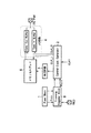
図15は、上記半導体記憶装置の典型的な構成を示すブロック図である。
【0007】
図15に示すように、半導体記憶装置は、総数n本のヒューズを含み、回路特性トリミング用のヒューズデータF<n>を出力するヒューズセットブロック(Fuse Block)1と、チップ内部の動作を制御する内部クロックCLK_P/CLK_O/CLK_Iの生成タイミングを、ヒューズデータF<n>により最適値にトリミングすることができるクロック生成回路(Control Clock Generator)2と、クロック生成回路2から生成される内部クロックCLK_P/CLK_O/CLK_Iにより制御される周辺回路3と、データ出力バッファ(Data Out Buffer)とデータ入力バッファ(Data In Buffer)との2回路からなるI/O回路4と、内部クロックにより制御されるこれら2つの回路3、4によってデータの読み書きが制御されるメモリセルアレイ5とを有する。
【0008】
図15に示す装置において、クロック生成回路2から生成される内部クロックCLK_P/CLK_O/CLK_Iは、それぞれ周辺回路3、I/O回路4内のデータ出力バッファ、およびデータ入力バッファを制御するための内部クロックである。
【0009】
周辺回路3は、内部クロックCLK_Pに同期して動作しているため、このクロックCLK_Pの生成タイミングを変えることで、周辺回路3内の動作タイミングを任意に変えることができる。
【0010】
データ出力バッファは、内部クロックCLK_Oの立ち上がりエッジ、あるいは立ち下がりエッジ、あるいは両エッジに同期してメモリセルアレイからデータをチップ外部に読み出すための回路であり、このクロックCLK_Oの生成タイミングを変えることで、データ出力のタイミングを任意に調整することができる。
【0011】
また、データ入力バッファは、内部クロックCLK_Iの立ち上がりエッジ、あるいは立ち下がりエッジ、あるいは両エッジに同期してメモリセルアレイに書き込むデータをチップ内部に取り込むための回路であり、このクロックCLK_Iの生成タイミングを変えることで、データ入力のタイミングを任意に調整することができる。
【0012】
次に、データ入力タイミングのトリミングの場合を例にして全体動作について説明する。
【0013】
図16Aは外部クロックCLKとデータDQとの関係を示す図、図16Bは内部クロックCLK_Iと入力データD_INとの関係(トリミング前)を示す図、図16Cは内部クロックCLK_Iと入力データD_INとの関係(トリミング後)を示す図である。
【0014】
図16Aに示すように、メモリセルアレイへの書き込みデータは、外部クロックCLKの立ち上がり、立ち下がりの両エッジに同期させ、DQ PADから入力される。このとき、データは、クロックに対して、データ入力バッファの回路動作マージンが最大となるようなタイミングで入力される。つまり、クロックの周期をTとするならば、ある入力データのクロックに対してのセットアップ時間Tsとホールド時間Thが共にT/4になるタイミングでデータを入力している。
【0015】
このようにチップ外部では、クロックとデータとの関係が最適となっているのだが、実際のチップ内部では、このような理想的な関係とはなっていないのが実状である。なぜなら、プロセス変動やチップ内部のLCRの影響などによって、内部クロックCLK_Iの発生タイミングにズレが生じてしまうからである。
【0016】
今、内部クロックCLK_Iのタイミングが上記のような要因で+Δtずれてしまっている、とする。この場合、図16Bに示すように、チップ内部データD_INに対するデータ入力のセットアップ時間TsiはT/4+Δtとなり、回路動作マージンが広がるが、データ入力のホールド時間ThiはT/4−Δtとなり、回路動作マージンは先程とは異なり小さくなってしまう。
【0017】
このような回路動作マージンの不均衡を修正するために、−Δtだけ内部クロックCLK_Iの発生タイミングを速めるヒューズをブローすることで、内部クロックCLK_Iのトリミングを行い、図16Cに示すように、内部タイミングを外部タイミングと揃え、回路動作の最適化を行う。
【0018】
【発明が解決しようとする課題】
しかしながら、実チップではプロセス変動の影響を受けているため、同一ヒューズをブローした場合でもトリミング値は必ずしも同一で無いと言うのが実状である。
【0019】
したがって、上記のようなヒューズブローによるトリミング手法は、ヒューズブローによるトリミングの効果、つまりブローしたヒューズが本当にそのチップに対して最適だったのかの判断は実際にヒューズをブローしてみなければ解らないという問題を抱えている。よって、時にはトリミング量が足りなかったり、超過気味だったりする場合も生じてしまう。
【0020】
つまり、従来技術のヒューズブローによるトリミングを行う手法では、そのチップに対して最適なトリミングを行うことが非常に困難である、という事情がある。
【0021】
また、チップのパッケージ封入前に行うレーザヒューズブローによる手法においては、そのヒューズが正しくブローされているか否かについては容易に確認できるが、チップのパッケージ封入後にエレクトリックヒューズを用いる場合では、そのヒューズが正しくブローされているか判断する手段がなく、実際にそのチップをテストしてみなければ解らないという事情も抱えている。
【0022】
以上は、クロック生成タイミングのトリミングに関しての事情であるが、行列アドレスのリダンダンシ置換の場合についても同様である。
【0023】
一般にリダンダンシによる行列アドレスの置換においては、ヒューズブローする前に、置換しようとする行列アドレスで決まるリダンダンシアレイのテストを行い、その結果に基づき、リダンダンシ置換を行っている。
【0024】
このリダンダンシセルテストは、あくまでそのセルが有効か否かをテストするためのものであり、実際のテストと同一タイミングでチップを動作させてテストしているわけではない。
【0025】
したがって、リダンダンシ置換後にテストしてみたらタイミングなどのミスマッチで動作しないという場合が生じてしまう場合がある。
【0026】
このような事情も、上記クロック生成タイミングのトリミングの場合と同様に、現状のヒューズブローによるトリミングやリダンダンシ置換の手法では、実際にヒューズをブローして見なければ、ヒューズブロー後のチップの状態を判断できないという事情に起因する。
【0027】
この発明は、上記の事情に鑑み為されたもので、その目的は、実際にヒューズをブローしなくても、ヒューズブロー後のチップの状態を判断できる半導体集積回路装置を提供することにある。
【0028】
また、他の目的は、歩留りを、さらに向上させることが可能な半導体集積回路装置の検査方法を提供することにある。
【0029】
【課題を解決するための手段】
本発明の第1態様に係る半導体集積回路装置は、複数のアドレス信号により選択される複数のメモリセルで構成されるメモリセルアレイと、外部クロック信号を受けて、複数の内部クロック信号を生成するクロック生成回路と、前記クロック生成回路で生成された第1のクロック信号に同期して、外部コマンド信号を取り込み、演算して、前記複数のアドレス信号、および複数の内部制御信号を発生する周辺回路と、前記クロック生成回路で生成された第2のクロック信号に同期して、外部データ信号を取り込み、内部データ信号線に転送する、および前記クロック生成回路で生成された第3のクロック信号に同期して、内部データ信号を取り込み、外部データ信号線に転送するI/O回路と、プログラム可能なヒューズ素子を含み、このヒューズ素子にプログラムされたデータを出力するヒューズ素子ブロックと、前記ヒューズ素子ブロックから出力されたデータ、あるいは外部から入力され、レジスタに格納された任意データのいずれかを、前記第1、第2、第3のクロック信号の生成タイミングをトリミングするデータとして、前記クロック生成回路へ転送し、前記ヒューズ素子ブロックから出力されたデータを、前記レジスタを介して外部に出力するトリミングレジスタ回路とを具備することを特徴としている。
【0030】
本発明の第2態様に係る半導体集積回路装置は、行列の複数のアドレス信号により選択される複数のメモリセルで構成されるメモリセルアレイと、外部クロック信号を受けて、複数の内部クロック信号を生成するクロック生成回路と、前記クロック生成回路で生成された第1のクロック信号に同期して、外部コマンド信号を取り込み、演算して、前記行列複数のアドレス信号、および複数の内部制御信号を発生する周辺回路と、前記クロック生成回路で生成された第2のクロック信号に同期して、外部データ信号を取り込み、内部データ信号線に転送する、および前記クロック生成回路で生成された第3のクロック信号に同期して、内部データ信号を取り込み、外部データ信号線に転送するI/O回路と、プログラム可能なヒューズ素子を含み、このヒューズ素子にプログラムされたデータを出力するヒューズ素子ブロックと、前記ヒューズ素子ブロックから出力されたデータ、あるいは外部から入力され、レジスタに格納された任意データのいずれかを、前記メモリセルアレイのリダンダンシ置換データとして、前記周辺回路へ転送し、前記ヒューズ素子ブロックから出力されたデータを、前記レジスタを介して外部に出力するトリミングレジスタ回路とを具備することを特徴としている。
【0031】
本発明の第3態様に係る半導体集積回路装置は、行列の複数のアドレス信号により選択される複数のメモリセルで構成されるメモリセルアレイと、外部クロック信号を受けて、複数の内部クロック信号を生成するクロック生成回路と、前記クロック生成回路で生成された第1のクロック信号に同期して、外部コマンド信号を取り込み、演算して、前記行列の複数のアドレス信号、および複数の内部制御信号を発生する周辺回路と、前記クロック生成回路で生成された第2のクロック信号に同期して、外部データ信号を取り込み、内部データ信号線に転送する、および前記クロック生成回路で生成された第3のクロック信号に同期して、内部データ信号を取り込み、外部データ信号線に転送するI/O回路と、プログラム可能なヒューズ素子を含み、このヒューズ素子にプログラムされたデータを出力するヒューズ素子ブロックと、前記ヒューズ素子ブロックから出力されたデータ、あるいは外部から入力され、レジスタに保持された任意データのいずれかを、前記第1、第2、第3のクロック信号の生成タイミングをトリミングするデータとして、前記クロック生成回路へ転送するとともに、前記ヒューズ素子ブロックから出力されたデータ、あるいは外部から入力され、前記レジスタに保持された任意データのいずれかを、前記メモリセルアレイのリダンダンシ置換データとして、前記周辺回路へ転送し、前記ヒューズ素子ブロックから出力されたデータを、前記レジスタを介して外部に出力するトリミングレジスタ回路とを具備することを特徴としている。
【0032】
本発明の第4態様に係る半導体集積回路装置は、半導体集積回路部と、プログラム可能なヒューズ素子を含むヒューズ素子ブロックと、データを格納するレジスタと、前記ヒューズ素子にプログラムされたデータの前記半導体集積回路部への転送、外部から前記レジスタに入力されたデータの前記半導体集積回路部への転送、及び前記レジスタを介した前記ヒューズ素子にプログラムされたデータの外部への転送のうちの1つを選択するデータ転送選択回路とを具備することを特徴としている。
本発明の第5態様に係る半導体集積回路装置は、半導体集積回路部と、プログラム可能なヒューズ素子を含むヒューズ素子ブロックと、レジスタとデータ転送選択回路を含み、前記レジスタは外部からの入力データを格納することが可能で、前記ヒューズ素子にプログラムされたデータを格納し、前記データ転送選択回路は、ヒューズ素子にプログラムされたデータの前記半導体集積回路部への転送、前記レジスタに格納されたデータの前記半導体集積回路部への転送、及び前記ヒューズ素子にプログラムされたデータの前記レジスタへの転送のうちの1つを選択するレジスタブロックとを具備することを特徴としている。
【0033】
本発明の第6態様に係る半導体集積回路装置の検査方法は、レジスタに、外部からトリミングデータを入力し、このトリミングデータに基づき半導体集積回路装置のトリミング効果を調べ、前記トリミング効果を調べた結果に基づいてトリミングデータを決定し、前記決定されたトリミングデータを前記半導体集積回路装置内に設けられたヒューズ素子にプログラムし、前記ヒューズ素子にプログラムされたトリミングデータを、前記レジスタを介して前記半導体集積回路装置の外部に読み出し、前記トリミングデータが前記ヒューズ素子に正しくプログラムされているか否かを確認し、前記トリミングデータが前記ヒューズ素子に正しくプログラムされていない場合、前記トリミングデータを前記半導体集積回路装置内に設けられたヒューズ素子に再度プログラムし、前記トリミングデータが前記ヒューズ素子に正しくプログラムされている場合、製品テストを行い、前記製品テストで不良が確認されたとき、前記トリミングデータが外部から前記半導体集積回路装置内の前記レジスタに入力されて前記トリミング効果が再度調べられ、前記トリミング効果を調べた結果に基づき再度前記トリミングデータが決定され、前記トリミングデータが前記半導体集積回路装置内に設けられた前記ヒューズ素子に再度プログラムされ、前記ヒューズ素子にプログラムされた前記トリミングデータが前記レジスタを介して前記半導体集積回路装置の外部に再度読み出され、前記トリミングデータが前記ヒューズ素子に正しくプログラムされているかどうかが再度確認され、前記トリミングデータがヒューズ素子に正しくプログラムされていない場合、前記トリミングデータが前記半導体集積回路装置に設けられた前記ヒューズ素子に再度プログラムされることを特徴としている。
【0034】
【発明の実施の形態】
以下、この発明の実施の形態を、図面を参照しながら説明する。この説明に際し、全図にわたり、共通する部分には共通する参照符号を付す。
【0035】
(第1実施形態)
図1は、この発明の第1実施形態に係わる半導体記憶装置の構成を示すブロック図である。
【0036】
図1に示すように、ヒューズセットブロック(Fuse Block)1は、レーザ、あるいは電流等の電気的手段により、ブローされる総数n本のヒューズを含み、これらヒューズがブローされているか否かを示すパラレルなヒューズデータF<1:n>を出力する。このパラレルなヒューズデータF<1:n>は、回路特性トリミング用のデータとして用いられる。
【0037】
クロック生成回路(Control Clock Generator)2は、外部クロック信号CLK1を受けて、チップ内部の動作を制御する複数の内部クロック信号CLK_P/CLK_O/CLK_Iを生成する。また、このクロック生成回路2は、上記内部クロックCLK_P/CLK_O/CLK_Iの生成タイミングを、上記ヒューズデータF<1:n>に基いて、最適な値にトリミングする。
【0038】
周辺回路3は、クロック生成回路2で生成された内部クロック信号CLK_Pにより動作が制御され、この内部クロック信号CLK_Pに同期して外部コマンド信号を取り込み、演算して行列の複数のアドレス信号、複数の内部制御信号を発生する。
【0039】
I/O回路4は、クロック生成回路2で生成された内部クロック信号CLK_Iに同期して、例えばqビットのデータ幅を持つ外部シリアルデータ信号を取り込み、この外部シリアルデータ信号をqビットのデータ幅を持つ内部シリアルデータ信号線に転送するデータ入力バッファ(Data In Buffer)、およびクロック生成回路2で生成された内部クロック信号CLK_Oに同期して、例えばqビットのデータ幅を持つ内部シリアルデータ信号を取り込み、この内部シリアルデータ信号をqビットのデータ幅を持つ外部シリアルデータ信号線に転送するデータ出力バッファ(Data Out Buffer)を含む。
【0040】
メモリセルアレイ5は、行列の複数のアドレス信号により選択される複数のメモリセルで構成されている。このメモリセルアレイ5へのデータの読み書きは、周辺回路3、I/O回路4によって制御される。
【0041】
さらに、本実施形態に係わる装置は、クロック生成回路2で生成される内部クロック信号CLK_P/CLK_O/CLK_Iの生成タイミングを微調整するトリミングデータ信号Ft<n>を出力するトリミングレジスタ回路(Trimming Register Block)6を有する。
【0042】
トリミングレジスタ回路6は、ヒューズセットブロック1から出力されたパラレルなヒューズデータF<1:n>、あるいはトリミングレジスタ回路6中に設けられているトリミングレジスタ(詳しくは後述する)から転送された、データの書き替えが可能なパラレルなデータR<1:n>のいずれかを、トリミングデータFt<1:n>として、切り替え出力する。
【0043】
図1に示す装置において、クロック生成回路2から生成される内部クロックCLK_P/CLK_O/CLK_Iは、それぞれ周辺回路3、I/O回路4内のデータ出力バッファ、およびデータ入力バッファを制御するための内部クロックである。
【0044】
本実施形態に係わる装置は、図2A〜図2Cに示すように、従来と同様、内部クロック生成のタイミングを変えることで、周辺回路3内の動作タイミング、データ入力のタイミング、データ出力のタイミングを最適値に調整することができる。
【0045】
次に、本実施形態におけるトリミングレジスタ回路6について説明する。
【0046】
図3は、本実施形態におけるトリミングレジスタ回路6の回路構成の一例を示す図である。
【0047】
図3に示すように、本実施形態におけるトリミングレジスタ回路6は、トリミングブロック(Trimming Block1〜Trimming Block3)11-1〜11-3と、nビットのデータの読み書きが自由にできるトリミングレジスタ(Trimming Register)12と、トリミングブロック(Trimming Block)選択回路13の、計3回路で構成されている。
【0048】
トリミングブロック(Trimming Block)11-1〜11-3は、CLK_O用/CLK_I用/CLK_P用の3つに分れており、それぞれが内部クロックCLK_O/CLK_P/CLK_Iをトリミングするのに必要なビット数と同数のn個のデータ(Data)転送選択回路14-1〜14-nから構成される。
【0049】
nビットのトリミングデータFt<1:n>を出力するn個のデータ転送選択回路14-1〜14-nは、それぞれ2つのトランスファゲートから構成されており、ヒューズセットからのデータF<1:n>、またはトリミングレジスタ12からのデータR<1:n>のどちらをトリミングデータFt<1:n>として出力するかを制御している。
【0050】
データ転送選択回路14-1〜14-n内の、トランスファゲートのゲートレベルの制御、ひいてはトリミングブロック11-1〜11-3の選択は、トリミングブロック選択回路13から出力される4つの制御信号PG1/NG1/PG2/NG2によってなされる。
【0051】
トリミングレジスタ12は、内部クロックCLK_O/CLK_P/CLK_Iをトリミングするのに必要なビット数と同ビット数の読み書き自由なレジスタである。
【0052】
トリミングブロック選択回路13は、トリミングを行う内部クロックに対応したトリミングブロック11-1〜11-3を選択するための制御信号PG1/NG1/PG2/NG2を作りだす。
【0053】
トリミングブロック11-1〜11-3は、上記4つの制御信号PG1/NG1/PG2/NG2の状態によって、(1)Normal状態、(2)Write状態、(3)Read状態の3状態に分けられる。
【0054】
次に、トリミングブロック選択回路13について説明する。
【0055】
図4Aは、本実施形態におけるトリミングブロック選択回路13の回路構成の一例を示す図である。
【0056】
図4Aに示すように、本実施形態におけるトリミングブロック選択回路13は、トリミングブロック選択レジスタ(Trimming Block選択Register)21と、データ転送制御ロジック部(Data転送制御Logic部1〜Data転送制御Logic部3)22-1〜22-3から構成されている。
【0057】
データ転送制御ロジック部22-1〜22-3は、上記トリミングブロック11-1〜11-3に対応する形で3つに分れている。データ転送制御ロジック部22-1〜22-3の状態は、トリミングブロック選択レジスタ21から出力される2ビットのアドレス信号(Add1/Add2)、およびトリミングブロックの状態を決めるモード信号Readによって決まる。
【0058】
図4Bは、内部クロックCLK_I用のトリミングブロック11-2に対するデータ転送制御ロジック部22-3の演算結果を表している。
【0059】
図4Bに示すように、トリミングブロック選択レジスタ21からのアドレスAdd1/Add2が、ともに“HIGH”でない場合、トリミングブロック11-2の状態は、常にNormal状態になる。反対に、アドレスAdd1/Add2が、ともに“HIGH”である場合、モード信号Readが“HIGH”の時、Read状態となり、“LOW”の時、Write状態となる。
【0060】
また、データ転送制御ロジック部22-1〜22-3中のNANDロジック回路に入力されるアドレスAdd1/Add2の状態によって、どのトリミングブロック11-1〜11-3が選択されるかが決まる。
【0061】
ここで、トリミングブロック11の3つの状態、(1)Normal状態、(2)Write状態、(3)Read状態について説明する。
【0062】
まず、(1)Normal状態から説明する。図5にNormal状態におけるトリミングブロック11中のデータ転送選択回路14の状態を示す。
【0063】
(1)Normal状態では、図5に示すように、トランスファゲートTRS1はON状態、トランスファゲートTRS2はOFF状態となっている。このため、クロック生成回路2へ出力されるトリミングデータFtは、ヒューズセットブロック1からのデータFとなり、内部クロックのトリミングは、このデータFに基づいて行わる。
【0064】
次に、(2)Write状態について説明する。図6にWrite状態におけるトリミングブロック11中のデータ転送選択回路14の状態を示す。
【0065】
(2)Write状態では、図6に示すように、トランスファゲートTRS1はOFF状態、トランスファゲートTRS2はON状態となっている。このため、クロック生成回路2へ出力されるトリミングデータFtは、トリミングレジスタ12からのデータRとなる。このトリミングレジスタ12からのデータRは、例えば外部パッドRIOからトリミングレジスタ12にデータを書き込むことで、自由に設定することができる。このため、内部クロックのトリミングを自由に行うことができる。
【0066】
最後に、(3)Read状態について説明する。図7にRead状態におけるトリミングブロック11中のデータ転送選択回路14の状態を示す。
【0067】
(3)Read状態では、図7に示すように、トランスファゲートTRS1、TRS2が、ともにON状態となっている。この結果、クロック生成回路2へ出力されるトリミングデータFtは、ヒューズセットブロック1からのデータFとなる。
【0068】
また、この場合、トランスファゲートTRS2もON状態になっているため、ヒューズセットブロック1からのデータF、つまりトリミングデータFtを、トリミングレジスタ12を用い、例えば外部パッドRIOを介して読み出すことができる。
【0069】
次に、ヒューズセットブロック1について説明する。
【0070】
図8は、本実施形態におけるヒューズセットブロック1の回路構成の一例を示す図である。
【0071】
図8に示すように、本実施形態のヒューズセットは、レーザヒューズブロック(Laser Fuse Block)31と、エレクトリックヒューズブロック(Electric Fuse Block)32とから構成されている。レーザヒューズブロック31には、例えばレーザ溶断型のヒューズが設けられ、エレクトリックヒューズブロック32には、例えば電流溶断型のヒューズが設けられる。
【0072】
このような構成にすることで、チップをパッケージ封入前にレーザヒューズでトリミングした後、パッケージ封入による影響で再トリミングが必要になった場合でも、再度、トリミングすることが可能となる。
【0073】
次に、トリミングレジスタ12について説明する。
【0074】
図9は本実施形態におけるトリミングレジスタ12とトリミングブロック11との関係を示す図、図10はトリミングレジスタ12の回路構成の一例を示す図である。なお、本回路構成例では、トリミングデータFtが8ビットの場合を想定する。
【0075】
図9、および図10に示すように、トリミングレジスタ12は、8個のフリップフロップ(FF)回路41-1〜41-8、8個のマルチプレクス(MX)回路42-1〜42-8、8個のWrite用出力回路43-1〜43-8、および1個のRead用出力回路44とを含む。
【0076】
本回路構成例におけるフリップフロップ回路41-1〜41-8の出力ノードfuse<1:n>はそれぞれ、マルチプレクス回路42-1〜42-8の第1入力に接続されるとともに、Write用出力回路43-1〜43-8の入力に接続される。
【0077】
Write用出力回路43-1〜43-8の出力はそれぞれ、トリミングレジスタ12とトリミングブロックとの接続ノードdREGbit<1:n>に接続される。さらに接続ノードdREGbit<1:n>はそれぞれ、マルチプレクス回路42-1〜42-8の第2入力に接続される。
【0078】
マルチプレクス回路42-1〜42-8はそれぞれ、信号fuse data enに基いて、出力ノードfuse<1:n>、あるいは接続ノードdREGbit<1:n>のいずれか一つを選択して、フリップフロップ回路41-2〜41-8の入力、およびRead用出力回路44の入力に接続する。
【0079】
Read用出力回路44の出力は、トリミングレジスタ12と外部パッドRIOとの接続ノードCore Dataに接続される。さらに接続ノードCore Dataは、フリップフロップ回路41-1〜41-8のうち、初段のフリップフロップ回路41-1の入力に接続される。
【0080】
次に、その動作を説明する。
【0081】
Write時、まず、フリップフロップ回路41-1〜41-8をそれぞれ、リセット信号fuse rstを用いてリセットする。
【0082】
さらに信号fuse data enを、例えば“HIGH”とし、マルチプレクス回路42-1〜42-7がそれぞれ、出力ノードfuse<1:7>を選択するようにしておく。なお、最終段のマルチプレクス回路42-8は、fuse data enの逆相の信号で制御され、Write時には、出力ノードfuse<8>を選択しない。
【0083】
この状態で、初段のフリップフロップ回路41-1の入力に、外部パッドRIOから、接続ノードCore Dataを介して、データをシリアルに入力する。フリップフロップ回路41-1〜41-8はそれぞれ、制御クロックfuse clkに同期して動作し、制御クロックfuse clkの立ち上がり、もしくは立ち下がりに応じて、入力されたデータを出力する。そして、例えば制御クロックfuse clkを8回トグルさせることで、8個のフリップフロップ回路41-1〜41-8それぞれにデータがセットされる。データがセットされた後、信号writeを、例えば“HIGH”レベルとし、Write用出力回路43-1〜43-8をそれぞれイネーブルする。この結果、フリップフロップ回路41-1〜41-8にセットされたデータが、データR<1:n>として、トリミングブロック11に対して出力される。これにより、トリミングブロック11からは、上述したように、データR<1:n>が、トリミングデータFt<1:n>として、クロック生成回路2に対して出力される。
【0084】
また、Read時、フリップフロップ回路41-1〜41-8をそれぞれ、リセット信号fuse rstを用いてリセットする。
【0085】
さらに、信号fuse data enは、最初に例えば“LOW”とし、マルチプレクス回路42-1〜42-7がそれぞれ、接続ノードdREGbit<1:7>を選択するようにしておく。なお、最終段のマルチプレクス回路42-8は、fuse data enの逆相の信号で制御されているので、このときには、接続ノードdREGbit<8>を選択していない。
【0086】
この状態では、初段のフリップフロップ回路41-2〜41-8の入力には、トリミングブロック11から、接続ノードdREGbit<1:7>を介して、ヒューズセットブロック1からのデータF<1:7>が入力されている。
【0087】
次に、信号fuse data enを、“LOW”から“HIGH”とし、マルチプレクス回路42-1〜42-7にそれぞれ、出力ノードfuse<1:7>を選択させる。これとともに、最終段のマルチプレクス回路42-8には、接続ノードdREGbit<8>を選択させる。これにより、Read用出力回路44には、ヒューズセットブロック1からのデータF<8>が入力される。この状態で、信号Readを、例えば“HIGH”レベルとし、Read用出力回路44をイネーブルすることで、データF<8>は、接続ノードCore Dataを介して、外部パッドRIOから出力される。
【0088】
次に、信号fuse data enを、再度“HIGH”から“LOW”とし、最終段のマルチプレクス回路42-8に、出力ノードfuse<8>を選択させる。これにより、Read用出力回路44には、フリップフロップ回路41-8にセットされていたヒューズセットブロック1からのデータF<7>が入力され、データF<8>に続いて、データF<7>が、接続ノードCore Dataを介して、外部パッドRIOから出力される。
【0089】
以下、上記動作を、データF<1>が出力されるまで繰り返すことで、ヒューズセットブロック1にセットされているデータF<1:8>を読み出すことができる。
【0090】
次に、本実施形態の全体動作について説明する。
【0091】
まず、データ入力タイミングのトリミングの場合について説明する。従来と同様、図2Bに示すようにチップ内部で内部クロックCLCK_Iが+Δtズレが生じてしまった場合、クロック発生回路で内部クロックCLK_Iの発生タイミングをΔt速めるトリミングを行わなければならない。
【0092】
トリミングを行う場合、従来はヒューズをブローしてみなければ実際のトリミング量などを調べることができなかったのだが、この発明では実際にヒューズをブローする前に、トリミングレジスタ回路6のトリミングブロック11の状態をWrite状態とし、トリミングレジスタ12を介して、ヒューズブローによるトリミング予定値と同じトリミングデータを書き込む。これにより、ヒューズをブローした状態と同じ状態でトリミング効果を調べることができる。
【0093】
この段階で、トリミングレジスタ回路6からのトリミングデータFtで、予定通りの効果があると判断できたならば、そこで初めてヒューズをブローすれば良い。
【0094】
反対にトリミング効果が不足、あるいは過剰だと判断された場合は、トリミングレジスタ回路6からのトリミングデータFtを、最適になるように調節して、その値に基づいてヒューズをブローすれば良い。
【0095】
図11に、この発明におけるトリミング手法の流れを示す。
【0096】
チップのパッケージ封入前、レーザヒューズによるトリミングを行う場合においても、まず、トリミングレジスタ回路6からのデータに基づきトリミングを行い、ヒューズブロー値を決める(ST.1)。
【0097】
次に、上記ヒューズブロー値に基いて、レーザヒューズをブローし(ST.2)、ヒューズが正しくブローされたかをトリミングレジスタを用いて確認する(ST.3)。
【0098】
もし、ブローされていなければ(NG)、再びヒューズブローの行程に戻り、再度ヒューズブローを行う。また、ヒューズが正しくブローされていることが確認できたら(OK)、チップをパッケージに封入する(ST.4)。
【0099】
次に、製品テストを行い(ST.5)、何ら問題が無いようであれば出荷する(ST.6)。
【0100】
もし、パッケージ封入の影響で再トリミングが必要になったならば(NG)、再度トリミングレジスタ回路6を用いて、今度はエレクトリックヒューズによるトリミングのヒューズ値を決める(ST.7)。
【0101】
次に、上記ヒューズ値に基いて、エレクトリックヒューズをブローし(ST.8)、ヒューズが正しくブローされたかをトリミングレジスタ回路6を用いて確認する(ST.9)。
【0102】
もし、ブローされていなければ(NG)、再びヒューズブローの行程に戻り、再度ヒューズブローを行う。また、ヒューズが正しくブローされていることが確認できたら(OK)、製品テストを行う(ST.10)。何ら問題が無いようであれば出荷する(ST.11)。
【0103】
もし、問題があった、例えば不良が確認されたときには(NG)、トリミングレジスタ回路6を用いて、再度ヒューズ値を決めてみることも可能である。
【0104】
以上のことから、この発明では、従来の様にヒューズをブローしてみて初めてトリミング効果が不足や超過だったと気づくようなことがなく、全てのチップに対して最適な値でトリミングすることができる。
【0105】
更に、この発明ではトリミングレジスタ回路6を用い、ヒューズが正しくブローされているか、その状態をパッケージ封入後でも容易に調べることができるため、エレクトリックヒューズを用いてヒューズブローする場合、ヒューズブローできているかどうかの検証にも効果がある。
【0106】
また、図11に示したトリミング手法によれば、ヒューズブローが不完全であった装置においても、再度救済することが可能となる。このため、歩留りを、さらに向上させることが可能となる。
【0107】
(第2実施形態)
図12Aはこの発明の第2実施形態に係わる半導体記憶装置の構成を示すブロック図、図12Bはそのヒューズセットブロックの構成を示す図である。
【0108】
図12Aに示すように、第2実施形態に係わる半導体記憶装置は、第1実施形態と同様、総数n本のヒューズデータF<n>を持つ回路特性トリミング用のヒューズセットブロック1と、ヒューズデータF<n>によりクロック発生のタイミングを最適値にトリミングすることができるクロック生成回路2と、クロック生成回路を制御するトリミングデータ信号Ft<n>を作り出すトリミングレジスタ回路6と、クロック生成回路2から生成される内部クロックにより制御される周辺回路3と、データ出力バッファ(Data Out Buffer)とデータ入力バッファ(Data In Buffer)との2回路からなるI/O回路4と、内部クロックにより制御されるこれら2つの回路によってデータの読み書きが制御されるメモリセルアレイ5とを有する。
【0109】
しかしながら、本第2実施形態では、図12Bに示すように、第1実施形態のヒューズセットブロック1の形態と異なり、ヒューズは、レーザヒューズ31のみで構成されている形態となっている。
【0110】
このような第2実施形態に係わる半導体記憶装置においても、第1実施形態と同様に、トリミングレジスタ回路6を用いて、ヒューズブローの効果を前もって確認することにより、最適なヒューズ値を決めることができ、全てのチップに対して最適な値でトリミングすることができる。
【0111】
(第3実施形態)
図13Aはこの発明の第3実施形態に係わる半導体記憶装置の構成を示すブロック図、図13Bはそのヒューズセットブロックの構成を示す図である。
【0112】
図13Aに示すように、第3実施形態に係わる半導体記憶装置は、第1実施形態と同様、総数n本のヒューズデータF<n>を持つ回路特性トリミング用のヒューズセットブロック1と、ヒューズデータF<n>によりクロック発生のタイミングを最適値にトリミングすることができるクロック生成回路2と、クロック生成回路を制御するトリミングデータ信号Ft<n>を作り出すトリミングレジスタ回路6と、クロック生成回路2から生成される内部クロックにより制御される周辺回路3と、データ出力バッファ(Data Out Buffer)とデータ入力バッファ(Data In Buffer)との2回路からなるI/O回路4と、内部クロックにより制御されるこれら2つの回路によってデータの読み書きが制御されるメモリセルアレイ5とを有する。
【0113】
しかしながら、本第3実施形態では、図13Bに示すように、第1、第2実施形態のヒューズセットの形態と異なり、ヒューズはエレクトリックヒューズ32のみで構成されている形態となっている。
【0114】
このような第3実施形態の半導体記憶装置においても、第1、第2実施形態と同様にトリミングレジスタ回路6を用いて、ヒューズブローの効果を前もって確認することにより、最適なヒューズ値を決めることができ、全てのチップに対して最適な値でトリミングすることができる。
【0115】
(第4実施形態)
図14は、この発明の第4実施形態に係わる半導体記憶装置の構成を示すブロック図である。
【0116】
図14に示すように、第4実施形態に係わる半導体記憶装置は、総数n本のヒューズデータF<n>を持つ回路特性トリミング用のヒューズ、および総数m本のヒューズデータF<m>を持つ行列アドレスのリダンダンシ置換用のヒューズからなるヒューズブロック1と、ヒューズデータF<n>によりクロック発生のタイミングを最適値にトリミングすることができるクロック生成回路2と、クロック生成回路2を制御するトリミングデータ信号Ft<n>並びに、行列アドレスのリダンダンシ置換を制御するリダンダンシデータ信号Fr<m>を作り出すトリミングレジスタ回路6と、クロック生成回路2から生成される内部クロック、並びにトリミングレジスタ回路6から出力されるリダンダンシデータ信号Fr<m>により制御される周辺回路3と、データ出力回路(Data Out Buffer)とデータ入力回路(Data In Buffer)の2回路からなるI/O回路4と、内部クロックにより制御されるこれら2つの回路によってデータの読み書きが制御されるメモリセルアレイ5とを有する。
【0117】
本第4実施形態においては、第1、第2、第3実施形態と同様に、トリミングレジスタ回路6を用いて、ヒューズブローの効果を前もって確認することにより、最適なヒューズ値を決めることができ、全てのチップに対して最適な値でトリミングすることができる。
【0118】
更に、本第4実施形態では、行列アドレスのリダンダンシ置換を行う際においても、ヒューズブローする前に、トリミングレジスタ回路を用いて、リダンダンシ置換がなされたと同等な状態にしてテストすることができるため、的確なリダンダンシ置換を行うことができる。
【0119】
上記第1〜第4実施形態を参照して説明したこの発明によれば、ヒューズブローによるチップ内部タイミングの微調整や行列アドレスのリダンダンシ置換を行う場合において、実際にヒューズをブローする前にレジスタ回路を用いて内部タイミングの微調整やリダンダンシ置換を行い、その結果に基づき実際にブローするヒューズ値を決める。
【0120】
また、前記レジスタ回路を用いてヒューズの状態を読み出すことで、ヒューズブローの成否を的確に判断したり、チップ毎のリダンダンシ置換情報を把握することができる。この手法により、タイミングの微調整を行う最適なヒューズ値をチップ毎に決めることができ、また的確な行列アドレスへのリダンダンシ置換を行うことが可能な半導体記憶装置を得ることができる。
【0121】
以上、この発明を第1〜第4実施形態により説明したが、この発明は、これら実施形態それぞれに限定されるものではなく、その実施にあたっては、発明の要旨を逸脱しない範囲で種々に変形することが可能である。
【0122】
また、上記各実施形態は、単独、または適宜組み合わせて実施することも勿論可能である。
【0123】
さらに、上記各実施形態には種々の段階の発明が含まれており、各実施形態において開示した複数の構成要件の適宜な組み合わせにより、種々の段階の発明を抽出することも可能である。
【0124】
【発明の効果】
以上説明したように、この発明によれば、実際にヒューズをブローしなくても、ヒューズブロー後のチップの状態を判断できる半導体記憶装置、および歩留りを、さらに向上させることが可能な半導体集積回路装置の検査方法をそれぞれ提供できる。
【図面の簡単な説明】
【図1】図1はこの発明の第1実施形態に係わる半導体記憶装置の構成を示すブロック図。
【図2】図2Aは外部クロックCLKとデータDQとの関係を示す図、図2Bは内部クロックCLK_Iと入力データD_INとの関係(トリミング前)を示す図、図2Cは内部クロックCLK_Iと入力データD_INとの関係(トリミング後)を示す図。
【図3】図3はトリミングレジスタ回路6の回路構成の一例を示す図。
【図4】図4Aはトリミングブロック選択回路13の回路構成の一例を示す図、図4Bはデータ転送制御ロジック部演算結果を表す図。
【図5】図5はNormal状態におけるデータ転送回路14の状態を示す図。
【図6】図6はWrite状態におけるデータ転送回路14の状態を示す図。
【図7】図7はRead状態におけるデータ転送回路14の状態を示す図。
【図8】図8はヒューズセットブロック1の回路構成の一例を示す図。
【図9】図9はトリミングレジスタ12とトリミングブロック11との関係を示す図。
【図10】図10はトリミングレジスタ12の回路構成の一例を示す図。
【図11】図11はこの発明におけるトリミング手法のフローチャート図。
【図12】図12Aはこの発明の第2実施形態に係わる半導体記憶装置の構成を示すブロック図、図12Bはそのヒューズセットブロックの構成を示す図。
【図13】図13Aはこの発明の第3実施形態に係わる半導体記憶装置の構成を示すブロック図、図13Bはそのヒューズセットブロックの構成を示す図。
【図14】図14はこの発明の第4実施形態に係わる半導体記憶装置の構成を示すブロック図。
【図15】図15は半導体記憶装置の典型的な構成を示すブロック図。
【図16】図16Aは外部クロックCLKとデータDQとの関係を示す図、図16Bは内部クロックCLK_Iと入力データD_INとの関係(トリミング前)を示す図、図16Cは内部クロックCLK_Iと入力データD_INとの関係(トリミング後)を示す図。
【符号の説明】
1…ヒューズセットブロック(Fuse Block)、
2…クロック生成回路(Control Clock Generator)、
3…周辺回路、
4…I/O回路、
5…メモリセルアレイ、
6…トリミングレジスタ回路(Trimming Register Block)、
11…トリミングブロック(Trimming Block)、
12…トリミングレジスタ(Trimming Register)、
13…トリミングブロック選択回路、
14…データ転送制御回路、
21…トリミングブロック選択レジスタ、
22…データ転送制御ロジック部、
31…レーザヒューズブロック(Laser Fuse Block)、
32…エレクトリックヒューズブロック(Electric Fuse Block)、
41…フリップフロップ回路、
42…マルチプレクス回路、
43…Write用出力回路、
44…Read用出力回路。[0001]
BACKGROUND OF THE INVENTION
The present invention relates to a semiconductor memory device, and more particularly to a technique and circuit configuration for fine adjustment of chip internal timing by fuse blow and replacement of redundancy.
[0002]
[Prior art]
2. Description of the Related Art In recent years, as semiconductor manufacturing processes are miniaturized and the speed of a semiconductor memory device is increased with an increase in system clock speed, the operation margin in the circuit is reduced, and optimization of circuit operation has become very difficult.
[0003]
In addition, it is further difficult to optimize the circuit operation because the characteristics of the transistor and the resistor are deviated from the initial design due to the influence of the process variation due to the complicated manufacturing process.
[0004]
In order to optimize circuit operation and improve yield, a fuse set for trimming circuit characteristics in consideration of the effects of such process variations and a fuse set for matrix address redundancy replacement are usually provided in the chip. It is.
[0005]
In the past, laser fuses that blow fuses such as polysilicon and metal with a laser beam were generally used. However, since laser fuses cannot be trimmed after the chip is encapsulated in the package, in recent years, However, electric fuses that can electrically blow fuses are being provided in chips.
[0006]
FIG. 15 is a block diagram showing a typical configuration of the semiconductor memory device.
[0007]
As shown in FIG. 15, the semiconductor memory device includes a total of n fuses, and fuse data F for circuit characteristic trimming. The fuse set block (Fuse Block) 1 that outputs <n> and the generation timing of the internal clock CLK_P / CLK_O / CLK_I that controls the internal operation of the chip are represented by the fuse data F A clock generation circuit (Control Clock Generator) 2 that can be trimmed to an optimum value by <n>, a
[0008]
In the apparatus shown in FIG. 15, the internal clocks CLK_P / CLK_O / CLK_I generated from the
[0009]
Since the
[0010]
The data output buffer is a circuit for reading data from the memory cell array to the outside of the chip in synchronization with the rising edge, falling edge, or both edges of the internal clock CLK_O. By changing the generation timing of this clock CLK_O, Data output timing can be arbitrarily adjusted.
[0011]
The data input buffer is a circuit for taking in data to be written into the memory cell array in synchronization with the rising edge, falling edge, or both edges of the internal clock CLK_I, and changes the generation timing of the clock CLK_I. Thus, the data input timing can be arbitrarily adjusted.
[0012]
Next, the overall operation will be described by taking the case of trimming data input timing as an example.
[0013]
16A shows the relationship between the external clock CLK and the data DQ, FIG. 16B shows the relationship between the internal clock CLK_I and the input data D_IN (before trimming), and FIG. 16C shows the relationship between the internal clock CLK_I and the input data D_IN. It is a figure which shows (after trimming).
[0014]
As shown in FIG. 16A, write data to the memory cell array is input from the DQ PAD in synchronization with both rising and falling edges of the external clock CLK. At this time, the data is input at a timing such that the circuit operation margin of the data input buffer is maximized with respect to the clock. In other words, if the clock cycle is T, data is input at a timing when both the setup time Ts and the hold time Th for the clock of certain input data are T / 4.
[0015]
As described above, the relationship between the clock and the data is optimal outside the chip, but the actual situation is that such an ideal relationship is not achieved inside the actual chip. This is because a deviation occurs in the generation timing of the internal clock CLK_I due to the process variation and the influence of the LCR inside the chip.
[0016]
Assume that the timing of the internal clock CLK_I has shifted by + Δt due to the above factors. In this case, as shown in FIG. 16B, the setup time Tsi of data input for the chip internal data D_IN is T / 4 + Δt and the circuit operation margin is widened, but the data input hold time Thi is T / 4−Δt and the circuit operation is The margin is smaller than before.
[0017]
In order to correct such circuit operation margin imbalance, the internal clock CLK_I is trimmed by blowing a fuse that accelerates the generation timing of the internal clock CLK_I by −Δt, and as shown in FIG. Is aligned with the external timing to optimize the circuit operation.
[0018]
[Problems to be solved by the invention]
However, since the actual chip is affected by process variations, the actual trimming value is not always the same even when the same fuse is blown.
[0019]
Therefore, the fuse blow trimming method as described above must be used to determine the effect of trimming by fuse blow, that is, whether the blown fuse was really optimal for the chip. Have a problem. Therefore, sometimes the trimming amount is insufficient or it is excessive.
[0020]
That is, there is a situation that it is very difficult to perform optimum trimming on the chip by the conventional technique of trimming by fuse blow.
[0021]
In addition, in the laser fuse blow method performed before the package of the chip, it can be easily confirmed whether or not the fuse is blown correctly. However, when an electric fuse is used after the package of the chip is used, the fuse is There is no way to determine if it is blown correctly, and there is a situation that you must understand by testing the chip.
[0022]
The above is the situation regarding the trimming of the clock generation timing, but the same applies to the case of redundancy replacement of the matrix address.
[0023]
In general, in replacement of a matrix address by redundancy, a redundancy array determined by a matrix address to be replaced is tested before fuse blowing, and redundancy replacement is performed based on the result.
[0024]
This redundancy cell test is only for testing whether or not the cell is valid, and does not test by operating the chip at the same timing as the actual test.
[0025]
Therefore, if the test is performed after redundancy replacement, there may be a case where the operation does not occur due to a mismatch of timing or the like.
[0026]
As in the case of the clock generation timing trimming described above, the current fuse blow trimming and redundancy replacement method also causes the state of the chip after fuse blow if the fuse is not actually blown. This is due to the fact that it cannot be judged.
[0027]
The present invention has been made in view of the above circumstances, and an object of the present invention is to provide a semiconductor integrated circuit device that can determine the state of a chip after blowing a fuse without actually blowing the fuse.
[0028]
Another object is to provide a method for inspecting a semiconductor integrated circuit device that can further improve the yield.
[0029]
[Means for Solving the Problems]
A semiconductor integrated circuit device according to a first aspect of the present invention includes a memory cell array including a plurality of memory cells selected by a plurality of address signals, and a clock that receives an external clock signal and generates a plurality of internal clock signals. And a peripheral circuit that captures and calculates an external command signal in synchronization with the first clock signal generated by the clock generation circuit, and generates the plurality of address signals and a plurality of internal control signals. In synchronization with the second clock signal generated by the clock generation circuit, the external data signal is taken in and transferred to the internal data signal line, and in synchronization with the third clock signal generated by the clock generation circuit. Including an I / O circuit for taking an internal data signal and transferring it to an external data signal line, and a programmable fuse element. A fuse element block for outputting the data programmed in over's device, the data output from the fuse element block or input from the outside Stored in the register Any one of the arbitrary data is transferred to the clock generation circuit as data for trimming the generation timing of the first, second, and third clock signals. The data output from the fuse element block is output to the outside through the register. And a trimming register circuit.
[0030]
A semiconductor integrated circuit device according to a second aspect of the present invention includes: Matrix A memory cell array composed of a plurality of memory cells selected by a plurality of address signals, a clock generation circuit that receives an external clock signal and generates a plurality of internal clock signals, and a first generated by the clock generation circuit A peripheral circuit that takes in and calculates an external command signal in synchronization with the clock signal and generates a plurality of address signals and a plurality of internal control signals, and a second clock generated by the clock generation circuit The external data signal is captured in synchronization with the signal, transferred to the internal data signal line, and the internal data signal is captured in synchronization with the third clock signal generated by the clock generation circuit, and is transferred to the external data signal line. Includes I / O circuit to transfer and programmable fuse element, and outputs data programmed in this fuse element A fuse element block that the data output from the fuse element block or input from the outside Stored in the register Any arbitrary data transferred to the peripheral circuit as redundancy replacement data of the memory cell array The data output from the fuse element block is output to the outside through the register. And a trimming register circuit.
[0031]
First of the present invention 3 A semiconductor integrated circuit device according to an aspect includes a memory cell array including a plurality of memory cells selected by a plurality of address signals in a matrix, a clock generation circuit that receives an external clock signal and generates a plurality of internal clock signals A peripheral circuit that captures and calculates an external command signal in synchronization with the first clock signal generated by the clock generation circuit, and generates a plurality of address signals of the matrix and a plurality of internal control signals; In synchronization with the second clock signal generated by the clock generation circuit, the external data signal is captured and transferred to the internal data signal line, and in synchronization with the third clock signal generated by the clock generation circuit. Includes an I / O circuit that takes in an internal data signal and transfers it to an external data signal line, and a programmable fuse element. A fuse element block for outputting the data programmed in over's device, the data output from the fuse element block or input from the outside Held in the register Is transferred to the clock generation circuit as data for trimming the generation timing of the first, second, and third clock signals, and the data output from the fuse element block or external Entered from Held in the register Any arbitrary data transferred to the peripheral circuit as redundancy replacement data of the memory cell array The data output from the fuse element block is output to the outside through the register. And a trimming register circuit.
[0032]
A semiconductor integrated circuit device according to a fourth aspect of the present invention includes a semiconductor integrated circuit unit, a fuse element block including a programmable fuse element, A register to store data; Transfer of data programmed in the fuse element to the semiconductor integrated circuit unit, from the outside In the register Transfer of input data to the semiconductor integrated circuit unit; and Through the register And a data transfer selection circuit for selecting one of the data transferred to the outside programmed in the fuse element.
A semiconductor integrated circuit device according to a fifth aspect of the present invention includes a semiconductor integrated circuit unit, a fuse element block including a programmable fuse element, a register and a data transfer selection circuit, and the register receives input data from the outside. Can be stored, Said Stores programmed data in the fuse element ,in front The data transfer selection circuit is configured to store the data programmed in the fuse element. semiconductor Transfer to integrated circuit section, register Store Of the generated data semiconductor And a register block for selecting one of transfer to the integrated circuit portion and transfer of data programmed in the fuse element to the register.
[0033]
First of the
[0034]
DETAILED DESCRIPTION OF THE INVENTION
Hereinafter, embodiments of the present invention will be described with reference to the drawings. In the description, common parts are denoted by common reference symbols throughout the drawings.
[0035]
(First embodiment)
FIG. 1 is a block diagram showing a configuration of a semiconductor memory device according to the first embodiment of the present invention.
[0036]
As shown in FIG. 1, a fuse set block (Fuse Block) 1 includes a total of n fuses to be blown by an electric means such as a laser or current, and indicates whether or not these fuses are blown. Parallel fuse data F Output <1: n>. This parallel fuse data F <1: n> is used as circuit characteristic trimming data.
[0037]
The clock generation circuit (Control Clock Generator) 2 receives the external clock signal CLK1 and generates a plurality of internal clock signals CLK_P / CLK_O / CLK_I for controlling the operation inside the chip. The
[0038]
The operation of the
[0039]
The I /
[0040]
The
[0041]
Furthermore, the apparatus according to the present embodiment includes a trimming data signal Ft for finely adjusting the generation timing of the internal clock signals CLK_P / CLK_O / CLK_I generated by the
[0042]
The
[0043]
In the apparatus shown in FIG. 1, internal clocks CLK_P / CLK_O / CLK_I generated from the
[0044]
As shown in FIGS. 2A to 2C, the apparatus according to the present embodiment changes the operation timing in the
[0045]
Next, the trimming
[0046]
FIG. 3 is a diagram showing an example of the circuit configuration of the
[0047]
As shown in FIG. 3, the trimming
[0048]
The trimming blocks (Trimming Blocks) 11-1 to 11-3 are divided into three for CLK_O / CLK_I / CLK_P, and the number of bits required for trimming the internal clock CLK_O / CLK_P / CLK_I, respectively. And n data (Data) transfer selection circuits 14-1 to 14-n.
[0049]
n-bit trimming data Ft Each of the n data transfer selection circuits 14-1 to 14-n that outputs <1: n> is composed of two transfer gates, and data F from the fuse set. <1: n> or data R from trimming
[0050]
The control of the gate level of the transfer gates in the data transfer selection circuits 14-1 to 14-n, and hence the selection of the trimming blocks 11-1 to 11-3, are performed by four control signals PG1 output from the trimming
[0051]
The trimming
[0052]
The trimming
[0053]
The trimming blocks 11-1 to 11-3 are divided into three states: (1) Normal state, (2) Write state, and (3) Read state, depending on the states of the four control signals PG1 / NG1 / PG2 / NG2. .
[0054]
Next, the trimming
[0055]
FIG. 4A is a diagram illustrating an example of a circuit configuration of the trimming
[0056]
As shown in FIG. 4A, the trimming
[0057]
The data transfer control logic units 22-1 to 22-3 are divided into three corresponding to the trimming blocks 11-1 to 11-3. The states of the data transfer control logic units 22-1 to 22-3 are determined by a 2-bit address signal (Add1 / Add2) output from the trimming
[0058]
FIG. 4B shows the calculation result of the data transfer control logic unit 22-3 for the trimming block 11-2 for the internal clock CLK_I.
[0059]
As shown in FIG. 4B, when the addresses Add1 / Add2 from the trimming
[0060]
Further, which trimming blocks 11-1 to 11-3 are selected is determined by the state of the addresses Add1 / Add2 input to the NAND logic circuits in the data transfer control logic units 22-1 to 22-3.
[0061]
Here, three states of the trimming block 11, (1) Normal state, (2) Write state, and (3) Read state will be described.
[0062]
First, (1) Normal state will be described. FIG. 5 shows the state of the data
[0063]
(1) In the Normal state, as shown in FIG. 5, the transfer gate TRS1 is in the ON state and the transfer gate TRS2 is in the OFF state. Therefore, trimming data Ft output to the
[0064]
Next, (2) Write state will be described. FIG. 6 shows the state of the data
[0065]
(2) In the Write state, as shown in FIG. 6, the transfer gate TRS1 is in the OFF state and the transfer gate TRS2 is in the ON state. Therefore, the trimming data Ft output to the
[0066]
Finally, (3) Read state will be described. FIG. 7 shows the state of the data
[0067]
(3) In the Read state, as shown in FIG. 7, both transfer gates TRS1 and TRS2 are in the ON state. As a result, the trimming data Ft output to the
[0068]
In this case, since the transfer gate TRS2 is also in the ON state, the data F from the fuse set
[0069]
Next, the fuse set
[0070]
FIG. 8 is a diagram illustrating an example of a circuit configuration of the fuse set
[0071]
As shown in FIG. 8, the fuse set of this embodiment includes a laser fuse block (Laser Fuse Block) 31 and an electric fuse block (Electric Fuse Block) 32. The
[0072]
With such a configuration, after the chip is trimmed with a laser fuse before enclosing the package, it is possible to perform trimming again even when re-trimming is required due to the effect of enclosing the package.
[0073]
Next, the trimming
[0074]
FIG. 9 is a diagram showing a relationship between the trimming
[0075]
As shown in FIGS. 9 and 10, the trimming
[0076]
Output node fuse of flip-flop circuits 41-1 to 41-8 in this circuit configuration example <1: n> is connected to the first inputs of the multiplex circuits 42-1 to 42-8, and to the inputs of the write output circuits 43-1 to 43-8.
[0077]
The outputs of the write output circuits 43-1 to 43-8 are respectively connected to the connection node dREGbit between the trimming
[0078]
Each of the multiplex circuits 42-1 to 42-8 is connected to the output node fuse based on the signal fuse data en. <1: n> or connection node dREGbit Any one of <1: n> is selected and connected to the inputs of the flip-flop circuits 41-2 to 41-8 and the input of the read
[0079]
The output of the read
[0080]
Next, the operation will be described.
[0081]
At the time of writing, first, the flip-flop circuits 41-1 to 41-8 are reset using the reset signal fuse rst.
[0082]
Further, the signal fuse data en is set to “HIGH”, for example, and the multiplex circuits 42-1 to 42-7 are respectively connected to the output nodes fuse. Make sure to select <1: 7>. Note that the multiplex circuit 42-8 at the final stage is controlled by a reverse-phase signal of fuse data en, and at the time of writing, the output node fuse Do not select <8>.
[0083]
In this state, data is serially input from the external pad RIO to the input of the first stage flip-flop circuit 41-1 via the connection node Core Data. Each of the flip-flop circuits 41-1 to 41-8 operates in synchronization with the control clock fuse clk, and outputs the input data according to the rise or fall of the control clock fuse clk. For example, data is set in each of the eight flip-flop circuits 41-1 to 41-8 by toggling the control clock fuse clk eight times. After the data is set, the signal write is set to “HIGH” level, for example, and the write output circuits 43-1 to 43-8 are enabled. As a result, the data set in the flip-flop circuits 41-1 to 41-8 becomes the data R It is output to the trimming block 11 as <1: n>. As a result, the trimming block 11 receives the data R as described above. <1: n> is the trimming data Ft It is output to the
[0084]
At the time of reading, the flip-flop circuits 41-1 to 41-8 are reset using the reset signal fuse rst.
[0085]
Further, the signal fuse data en is first set to, for example, “LOW”, and the multiplex circuits 42-1 to 42-7 are connected to the connection node dREGbit. Make sure to select <1: 7>. Note that the multiplex circuit 42-8 at the final stage is controlled by the reverse phase signal of the fuse data en, so at this time, the connection node dREGbit <8> is not selected.
[0086]
In this state, the input of the first stage flip-flop circuits 41-2 to 41-8 is supplied from the trimming block 11 to the connection node dREGbit. Data F from fuse set
[0087]
Next, the signal fuse data en is changed from “LOW” to “HIGH”, and the output nodes “fuse” are sent to the multiplex circuits 42-1 to 42-7, respectively. Select <1: 7>. At the same time, the multiplex circuit 42-8 at the final stage has a connection node dREGbit. Select <8>. As a result, the read
[0088]
Next, the signal fuse data en is changed from “HIGH” to “LOW” again, and the output node fuse is sent to the multiplex circuit 42-8 in the final stage. Select <8>. As a result, the read
[0089]
Hereinafter, the above operation is performed using the data F By repeating until <1> is output, data F set in fuse set
[0090]
Next, the overall operation of this embodiment will be described.
[0091]
First, the case of trimming data input timing will be described. As in the conventional case, as shown in FIG. 2B, when the internal clock CLCK_I shifts by + Δt in the chip, the clock generation circuit must perform trimming to accelerate the generation timing of the internal clock CLK_I by Δt.
[0092]
When trimming is performed, the actual trimming amount or the like cannot be checked unless the fuse is blown. However, in the present invention, before actually blowing the fuse, the trimming block 11 of the
[0093]
At this stage, if it can be determined that the trimming data Ft from the trimming
[0094]
On the other hand, when it is determined that the trimming effect is insufficient or excessive, the trimming data Ft from the trimming
[0095]
FIG. 11 shows the flow of the trimming technique in the present invention.
[0096]
Even when trimming with a laser fuse is performed before enclosing the chip package, first, trimming is performed based on data from the trimming
[0097]
Next, based on the fuse blow value, the laser fuse is blown (ST. 2), and it is confirmed using the trimming register whether the fuse has been blown correctly (ST. 3).
[0098]
If it is not blown (NG), the process returns to the fuse blowing process again, and the fuse is blown again. If it is confirmed that the fuse is blown correctly (OK), the chip is enclosed in a package (ST.4).
[0099]
Next, a product test is performed (ST. 5), and if there is no problem, the product is shipped (ST. 6).
[0100]
If re-trimming becomes necessary due to the influence of the package (NG), the trimming
[0101]
Next, based on the fuse value, the electric fuse is blown (ST. 8), and it is confirmed by using the
[0102]
If it is not blown (NG), the process returns to the fuse blowing process again, and the fuse is blown again. If it is confirmed that the fuse is blown correctly (OK), a product test is performed (ST. 10). If there is no problem, the product is shipped (ST. 11).
[0103]
If there is a problem, for example, if a defect is confirmed (NG), it is possible to determine the fuse value again using the
[0104]
As described above, according to the present invention, it is possible to perform trimming with an optimum value for all the chips without realizing that the trimming effect is insufficient or excessive only after the fuse is blown as in the prior art. .
[0105]
Further, in the present invention, the trimming
[0106]
Further, according to the trimming technique shown in FIG. 11, even in an apparatus in which fuse blow is incomplete, it is possible to rescue again. For this reason, the yield can be further improved.
[0107]
(Second Embodiment)
FIG. 12A is a block diagram showing the configuration of the semiconductor memory device according to the second embodiment of the present invention, and FIG. 12B is a diagram showing the configuration of the fuse set block.
[0108]
As shown in FIG. 12A, the semiconductor memory device according to the second embodiment has a total number n of fuse data F as in the first embodiment. Fuse set
[0109]
However, in the second embodiment, as shown in FIG. 12B, unlike the fuse set
[0110]
Also in the semiconductor memory device according to the second embodiment, the optimum fuse value can be determined by confirming the effect of fuse blow in advance using the
[0111]
(Third embodiment)
FIG. 13A is a block diagram showing the configuration of the semiconductor memory device according to the third embodiment of the present invention, and FIG. 13B is a diagram showing the configuration of the fuse set block.
[0112]
As shown in FIG. 13A, the semiconductor memory device according to the third embodiment has a total number n of fuse data F as in the first embodiment. Fuse set
[0113]
However, in the third embodiment, as shown in FIG. 13B, unlike the fuse set of the first and second embodiments, the fuse is configured by only the
[0114]
Also in the semiconductor memory device of the third embodiment, the optimum fuse value is determined by confirming the effect of fuse blow in advance using the
[0115]
(Fourth embodiment)
FIG. 14 is a block diagram showing a configuration of a semiconductor memory device according to the fourth embodiment of the present invention.
[0116]
As shown in FIG. 14, the semiconductor memory device according to the fourth embodiment has a total number n of fuse data F. Circuit characteristic trimming fuse having <n> and a total of m fuse data
[0117]
In the fourth embodiment, as in the first, second, and third embodiments, the optimum fuse value can be determined by confirming the effect of fuse blow in advance using the
[0118]
Furthermore, in the fourth embodiment, even when performing redundancy replacement of the matrix address, it is possible to perform a test in a state equivalent to the redundancy replacement using the trimming register circuit before blowing the fuse. Accurate redundancy replacement can be performed.
[0119]
According to the present invention described with reference to the first to fourth embodiments, in the case where fine adjustment of the internal timing of the chip by the blow of the fuse or the redundancy replacement of the matrix address is performed, the register circuit is actually blown before the fuse is blown. Is used for fine adjustment of internal timing and redundancy replacement, and the fuse value to be actually blown is determined based on the result.
[0120]
Further, by reading the state of the fuse using the register circuit, it is possible to accurately determine the success or failure of the blow of the fuse, or to know the redundancy replacement information for each chip. By this method, it is possible to determine an optimum fuse value for fine adjustment of timing for each chip and to obtain a semiconductor memory device capable of performing redundancy replacement to an accurate matrix address.
[0121]
As mentioned above, although this invention was demonstrated by 1st-4th embodiment, this invention is not limited to each of these embodiment, In the implementation, it changes variously in the range which does not deviate from the summary of invention. It is possible.
[0122]
Moreover, it is of course possible to implement each of the above embodiments singly or in appropriate combination.
[0123]
Furthermore, the above embodiments include inventions at various stages, and the inventions at various stages can be extracted by appropriately combining a plurality of constituent elements disclosed in the embodiments.
[0124]
【The invention's effect】
As described above, according to the present invention, the semiconductor memory device that can determine the state of the chip after the fuse is blown without actually blowing the fuse, and the semiconductor integrated circuit that can further improve the yield Each device inspection method can be provided.
[Brief description of the drawings]
FIG. 1 is a block diagram showing a configuration of a semiconductor memory device according to a first embodiment of the present invention.
2A is a diagram showing a relationship between an external clock CLK and data DQ, FIG. 2B is a diagram showing a relationship between the internal clock CLK_I and input data D_IN (before trimming), and FIG. 2C is a diagram showing the internal clock CLK_I and input data; The figure which shows the relationship (after trimming) with D_IN.
FIG. 3 is a diagram illustrating an example of a circuit configuration of a
4A is a diagram illustrating an example of a circuit configuration of a trimming
FIG. 5 is a diagram showing a state of the
FIG. 6 is a diagram showing a state of the
FIG. 7 is a diagram showing a state of the
FIG. 8 is a diagram showing an example of a circuit configuration of the fuse set
FIG. 9 is a diagram showing a relationship between the trimming
10 is a diagram illustrating an example of a circuit configuration of a trimming
FIG. 11 is a flowchart of a trimming method according to the present invention.
12A is a block diagram showing a configuration of a semiconductor memory device according to a second embodiment of the present invention, and FIG. 12B is a diagram showing a configuration of its fuse set block.
FIG. 13A is a block diagram showing a configuration of a semiconductor memory device according to a third embodiment of the present invention, and FIG. 13B is a diagram showing a configuration of its fuse set block.
FIG. 14 is a block diagram showing a configuration of a semiconductor memory device according to a fourth embodiment of the present invention.
FIG. 15 is a block diagram showing a typical configuration of a semiconductor memory device.
16A is a diagram showing a relationship between an external clock CLK and data DQ, FIG. 16B is a diagram showing a relationship between the internal clock CLK_I and input data D_IN (before trimming), and FIG. 16C is a diagram showing the internal clock CLK_I and input data; The figure which shows the relationship (after trimming) with D_IN.
[Explanation of symbols]
1 ... Fuse Block,
2 ... Clock generation circuit (Control Clock Generator),
3 Peripheral circuit,
4 ... I / O circuit,
5 ... Memory cell array,
6. Trimming register block (Trimming Register Block)
11 ... Trimming Block,
12 ... Trimming Register,
13 ... Trimming block selection circuit,
14: Data transfer control circuit,
21 ... Trimming block selection register,
22 ... Data transfer control logic part,
31 ... Laser Fuse Block,
32 ... Electric Fuse Block,
41 ... flip-flop circuit,
42. Multiplex circuit,
43 ... Output circuit for writing,
44: Read output circuit.
Claims (6)
外部クロック信号を受けて、複数の内部クロック信号を生成するクロック生成回路と、
前記クロック生成回路で生成された第1のクロック信号に同期して、外部コマンド信号を取り込み、演算して、前記複数のアドレス信号、および複数の内部制御信号を発生する周辺回路と、
前記クロック生成回路で生成された第2のクロック信号に同期して、外部データ信号を取り込み、内部データ信号線に転送する、および前記クロック生成回路で生成された第3のクロック信号に同期して、内部データ信号を取り込み、外部データ信号線に転送するI/O回路と、
プログラム可能なヒューズ素子を含み、このヒューズ素子にプログラムされたデータを出力するヒューズ素子ブロックと、
前記ヒューズ素子ブロックから出力されたデータ、あるいは外部から入力され、レジスタに格納された任意データのいずれかを、前記第1、第2、第3のクロック信号の生成タイミングをトリミングするデータとして、前記クロック生成回路へ転送し、前記ヒューズ素子ブロックから出力されたデータを、前記レジスタを介して外部に出力するトリミングレジスタ回路と
を具備することを特徴とする半導体集積回路装置。A memory cell array composed of a plurality of memory cells selected by a plurality of address signals;
A clock generation circuit that receives an external clock signal and generates a plurality of internal clock signals;
A peripheral circuit that captures and calculates an external command signal in synchronization with the first clock signal generated by the clock generation circuit, and generates the plurality of address signals and a plurality of internal control signals;
In synchronization with the second clock signal generated by the clock generation circuit, the external data signal is captured and transferred to the internal data signal line, and in synchronization with the third clock signal generated by the clock generation circuit. An I / O circuit that takes in an internal data signal and transfers it to an external data signal line;
A fuse element block including a programmable fuse element and outputting data programmed in the fuse element;
Either data output from the fuse element block or arbitrary data input from the outside and stored in a register is used as data for trimming the generation timing of the first, second, and third clock signals. A semiconductor integrated circuit device comprising: a trimming register circuit which transfers to a clock generation circuit and outputs data output from the fuse element block to the outside via the register.
外部クロック信号を受けて、複数の内部クロック信号を生成するクロック生成回路と、
前記クロック生成回路で生成された第1のクロック信号に同期して、外部コマンド信号を取り込み、演算して、前記行列複数のアドレス信号、および複数の内部制御信号を発生する周辺回路と、
前記クロック生成回路で生成された第2のクロック信号に同期して、外部データ信号を取り込み、内部データ信号線に転送する、および前記クロック生成回路で生成された第3のクロック信号に同期して、内部データ信号を取り込み、外部データ信号線に転送するI/O回路と、
プログラム可能なヒューズ素子を含み、このヒューズ素子にプログラムされたデータを出力するヒューズ素子ブロックと、
前記ヒューズ素子ブロックから出力されたデータ、あるいは外部から入力され、レジスタに格納された任意データのいずれかを、前記メモリセルアレイのリダンダンシ置換データとして、前記周辺回路へ転送し、前記ヒューズ素子ブロックから出力されたデータを、前記レジスタを介して外部に出力するトリミングレジスタ回路と
を具備することを特徴とする半導体集積回路装置。A memory cell array composed of a plurality of memory cells selected by a plurality of address signals of the matrix ;
A clock generation circuit that receives an external clock signal and generates a plurality of internal clock signals;
A peripheral circuit that captures and calculates an external command signal in synchronization with a first clock signal generated by the clock generation circuit, and generates a plurality of address signals of the matrix and a plurality of internal control signals;
In synchronization with the second clock signal generated by the clock generation circuit, the external data signal is captured and transferred to the internal data signal line, and in synchronization with the third clock signal generated by the clock generation circuit. An I / O circuit that takes in an internal data signal and transfers it to an external data signal line;
A fuse element block including a programmable fuse element and outputting data programmed in the fuse element;
Either data output from the fuse element block or arbitrary data input from the outside and stored in a register is transferred to the peripheral circuit as redundancy replacement data of the memory cell array, and output from the fuse element block And a trimming register circuit for outputting the processed data to the outside through the register.
外部クロック信号を受けて、複数の内部クロック信号を生成するクロック生成回路と、
前記クロック生成回路で生成された第1のクロック信号に同期して、外部コマンド信号を取り込み、演算して、前記行列の複数のアドレス信号、および複数の内部制御信号を発生する周辺回路と、
前記クロック生成回路で生成された第2のクロック信号に同期して、外部データ信号を取り込み、内部データ信号線に転送する、および前記クロック生成回路で生成された第3のクロック信号に同期して、内部データ信号を取り込み、外部データ信号線に転送するI/O回路と、
プログラム可能なヒューズ素子を含み、このヒューズ素子にプログラムされたデータを出力するヒューズ素子ブロックと、
前記ヒューズ素子ブロックから出力されたデータ、あるいは外部から入力され、レジスタに保持された任意データのいずれかを、前記第1、第2、第3のクロック信号の生成タイミングをトリミングするデータとして、前記クロック生成回路へ転送するとともに、前記ヒューズ素子ブロックから出力されたデータ、あるいは外部から入力され、前記レジスタに保持された任意データのいずれかを、前記メモリセルアレイのリダンダンシ置換データとして、前記周辺回路へ転送し、前記ヒューズ素子ブロックから出力されたデータを、前記レジスタを介して外部に出力するトリミングレジスタ回路とを具備することを特徴とする半導体集積回路装置。A memory cell array composed of a plurality of memory cells selected by a plurality of address signals of the matrix;
A clock generation circuit that receives an external clock signal and generates a plurality of internal clock signals;
A peripheral circuit that captures and calculates an external command signal in synchronization with the first clock signal generated by the clock generation circuit, and generates a plurality of address signals of the matrix and a plurality of internal control signals;
In synchronization with the second clock signal generated by the clock generation circuit, the external data signal is captured and transferred to the internal data signal line, and in synchronization with the third clock signal generated by the clock generation circuit. An I / O circuit that takes in an internal data signal and transfers it to an external data signal line;
A fuse element block including a programmable fuse element and outputting data programmed in the fuse element;
Either data output from the fuse element block or arbitrary data input from the outside and held in a register is used as data for trimming the generation timing of the first, second, and third clock signals. While transferring to the clock generation circuit, either the data output from the fuse element block or the arbitrary data input from the outside and held in the register is used as redundancy replacement data for the memory cell array to the peripheral circuit. A semiconductor integrated circuit device comprising: a trimming register circuit that transfers and outputs data output from the fuse element block to the outside through the register.
プログラム可能なヒューズ素子を含むヒューズ素子ブロックと、
データを格納するレジスタと、
前記ヒューズ素子にプログラムされたデータの前記半導体集積回路部への転送、外部から前記レジスタに入力されたデータの前記半導体集積回路部への転送、及び前記レジスタを介した前記ヒューズ素子にプログラムされたデータの外部への転送のうちの1つを選択するデータ転送選択回路と
を具備することを特徴とする半導体集積回路装置。A semiconductor integrated circuit section;
A fuse element block including a programmable fuse element;
A register to store data;
Transfer of data programmed in the fuse element to the semiconductor integrated circuit unit, transfer of data input from the outside to the register to the semiconductor integrated circuit unit, and programming to the fuse element via the register A semiconductor integrated circuit device comprising: a data transfer selection circuit that selects one of data transfers to the outside.
プログラム可能なヒューズ素子を含むヒューズ素子ブロックと、
レジスタとデータ転送選択回路を含み、前記レジスタは外部からの入力データを格納することが可能で、前記ヒューズ素子にプログラムされたデータを格納し、前記データ転送選択回路は、ヒューズ素子にプログラムされたデータの前記半導体集積回路部への転送、前記レジスタに格納されたデータの前記半導体集積回路部への転送、及び前記ヒューズ素子にプログラムされたデータの前記レジスタへの転送のうちの1つを選択するレジスタブロックと
を具備することを特徴とする半導体集積回路装置。A semiconductor integrated circuit section;
A fuse element block including a programmable fuse element;
Includes a register and a data transfer selection circuit, the register may store the input data from the outside, the fuse element to store the program data to, before Symbol data transfer selection circuit is programmed in the fuse element transfer to the semiconductor integrated circuit of the data transfer to the semiconductor integrated circuit of the data stored in the register, and one of the transfer to the register of the programmed data in the fuse element And a register block to be selected.
前記トリミング効果を調べた結果に基づいてトリミングデータを決定し、
前記決定されたトリミングデータを前記半導体集積回路装置内に設けられたヒューズ素子にプログラムし、
前記ヒューズ素子にプログラムされたトリミングデータを、前記レジスタを介して前記半導体集積回路装置の外部に読み出し、
前記トリミングデータが前記ヒューズ素子に正しくプログラムされているか否かを確認し、
前記トリミングデータが前記ヒューズ素子に正しくプログラムされていない場合、前記トリミングデータを前記半導体集積回路装置内に設けられたヒューズ素子に再度プログラムし、
前記トリミングデータが前記ヒューズ素子に正しくプログラムされている場合、製品テストを行い、
前記製品テストで不良が確認されたとき、前記トリミングデータが外部から前記半導体集積回路装置内の前記レジスタに入力されて前記トリミング効果が再度調べられ、前記トリミング効果を調べた結果に基づき再度前記トリミングデータが決定され、前記トリミングデータが前記半導体集積回路装置内に設けられた前記ヒューズ素子に再度プログラムされ、前記ヒューズ素子にプログラムされた前記トリミングデータが前記レジスタを介して前記半導体集積回路装置の外部に再度読み出され、前記トリミングデータが前記ヒューズ素子に正しくプログラムされているかどうかが再度確認され、前記トリミングデータがヒューズ素子に正しくプログラムされていない場合、前記トリミングデータが前記半導体集積回路装置に設けられた前記ヒューズ素子に再度プログラムされることを特徴とする半導体集積回路装置の検査方法。Trimming data is input to the register from the outside, and the trimming effect of the semiconductor integrated circuit device is examined based on this trimming data .
Determine trimming data based on the results of examining the trimming effect,
Programming the determined trimming data into a fuse element provided in the semiconductor integrated circuit device;
Trimming data programmed in the fuse element is read out of the semiconductor integrated circuit device through the register ,
Check whether the trimming data is correctly programmed in the fuse element,
When the trimming data is not correctly programmed in the fuse element, the trimming data is reprogrammed into the fuse element provided in the semiconductor integrated circuit device,
If the trimming data is correctly programmed into the fuse element, perform a product test,
When a defect is confirmed in the product test, the trimming data is externally input to the register in the semiconductor integrated circuit device, the trimming effect is checked again, and the trimming is performed again based on the result of checking the trimming effect. Data is determined, the trimming data is reprogrammed in the fuse element provided in the semiconductor integrated circuit device, and the trimming data programmed in the fuse element is external to the semiconductor integrated circuit device via the register. When the trimming data is correctly programmed in the fuse element, the trimming data is provided in the semiconductor integrated circuit device when the trimming data is not correctly programmed in the fuse element. Said hi A method of inspecting a semiconductor integrated circuit device characterized in that it is re-programmed to chromatography's device.
Priority Applications (3)
| Application Number | Priority Date | Filing Date | Title |
|---|---|---|---|
| JP2000305402A JP4723714B2 (en) | 2000-10-04 | 2000-10-04 | Semiconductor integrated circuit device and inspection method thereof |
| US09/971,371 US6490219B2 (en) | 2000-10-04 | 2001-10-03 | Semiconductor integrated circuit device and method of manufacturing thereof |
| US10/272,243 US6665226B2 (en) | 2000-10-04 | 2002-10-15 | Semiconductor integrated circuit device and method of manufacturing thereof |
Applications Claiming Priority (1)
| Application Number | Priority Date | Filing Date | Title |
|---|---|---|---|
| JP2000305402A JP4723714B2 (en) | 2000-10-04 | 2000-10-04 | Semiconductor integrated circuit device and inspection method thereof |
Publications (3)
| Publication Number | Publication Date |
|---|---|
| JP2002117694A JP2002117694A (en) | 2002-04-19 |
| JP2002117694A5 JP2002117694A5 (en) | 2007-11-22 |
| JP4723714B2 true JP4723714B2 (en) | 2011-07-13 |
Family
ID=18786272
Family Applications (1)
| Application Number | Title | Priority Date | Filing Date |
|---|---|---|---|
| JP2000305402A Expired - Fee Related JP4723714B2 (en) | 2000-10-04 | 2000-10-04 | Semiconductor integrated circuit device and inspection method thereof |
Country Status (2)
| Country | Link |
|---|---|
| US (2) | US6490219B2 (en) |
| JP (1) | JP4723714B2 (en) |
Families Citing this family (23)
| Publication number | Priority date | Publication date | Assignee | Title |
|---|---|---|---|---|
| KR100328447B1 (en) * | 2000-02-21 | 2002-03-16 | 박종섭 | Antifuse repair circuit |
| US6166981A (en) * | 2000-02-25 | 2000-12-26 | International Business Machines Corporation | Method for addressing electrical fuses |
| JP3884374B2 (en) * | 2002-12-06 | 2007-02-21 | 株式会社東芝 | Semiconductor device |
| DE10325769B4 (en) * | 2003-06-05 | 2007-01-04 | Zentrum Mikroelektronik Dresden Ag | Arrangement and method for balancing a calibratable current source |
| US7089136B2 (en) * | 2003-07-18 | 2006-08-08 | International Business Machines Corporation | Method for reduced electrical fusing time |
| JP3964841B2 (en) * | 2003-08-29 | 2007-08-22 | 株式会社東芝 | Semiconductor integrated circuit device |
| JP2005092915A (en) * | 2003-09-12 | 2005-04-07 | Toshiba Corp | Semiconductor integrated circuit device and information storage method for same |
| US20060044899A1 (en) * | 2004-08-27 | 2006-03-02 | Ellis Robert W | Method and apparatus for destroying flash memory |
| CN100481439C (en) * | 2004-10-27 | 2009-04-22 | 联咏科技股份有限公司 | Apparatus and method for multiple programming using one-time programmable device |
| JP4828901B2 (en) * | 2005-09-22 | 2011-11-30 | 株式会社東芝 | Semiconductor integrated circuit device |
| JP2007102848A (en) * | 2005-09-30 | 2007-04-19 | Toshiba Corp | Semiconductor integrated circuit device |
| JP2007102865A (en) * | 2005-09-30 | 2007-04-19 | Toshiba Corp | Semiconductor integrated circuit system |
| JP2008053259A (en) * | 2006-08-22 | 2008-03-06 | Fujitsu Ltd | Semiconductor integrated circuit and test method thereof |
| JP5003106B2 (en) * | 2006-11-06 | 2012-08-15 | セイコーエプソン株式会社 | Memory circuit inspection method |
| JP2008305517A (en) * | 2007-06-11 | 2008-12-18 | Hitachi Ulsi Systems Co Ltd | Semiconductor integrated circuit |
| US7532027B2 (en) * | 2007-09-28 | 2009-05-12 | Adtron, Inc. | Deliberate destruction of integrated circuits |
| KR101586325B1 (en) * | 2009-11-09 | 2016-02-03 | 삼성전자주식회사 | Trim circuit and semiconductor memory device including the same |
| US9343184B2 (en) | 2014-04-07 | 2016-05-17 | Micron Technology, Inc. | Soft post package repair of memory devices |
| US9741403B2 (en) * | 2014-11-12 | 2017-08-22 | Micron Technology, Inc. | Apparatuses and methods to perform post package trim |
| US9349491B1 (en) | 2015-04-17 | 2016-05-24 | Micron Technology, Inc. | Repair of memory devices using volatile and non-volatile memory |
| US10832791B2 (en) | 2019-01-24 | 2020-11-10 | Micron Technology, Inc. | Apparatuses and methods for soft post-package repair |
| US10629282B1 (en) * | 2019-06-16 | 2020-04-21 | Elite Semiconductor Memory Technology Inc. | E-fuse circuit |
| US11984185B2 (en) | 2021-04-07 | 2024-05-14 | Micron Technology, Inc. | Apparatuses and methods for zone-based soft post-package repair |
Family Cites Families (10)
| Publication number | Priority date | Publication date | Assignee | Title |
|---|---|---|---|---|
| JP2773271B2 (en) * | 1989-07-26 | 1998-07-09 | 日本電気株式会社 | Semiconductor storage device |
| JP2720718B2 (en) * | 1992-07-09 | 1998-03-04 | 株式会社デンソー | Semiconductor sensor device |
| US5682346A (en) * | 1995-03-29 | 1997-10-28 | Kabushiki Kaisha Toshiba | Nonvolatile semiconductor memory device having suitable writing efficiency |
| JP2000163999A (en) * | 1998-11-20 | 2000-06-16 | Fujitsu Ltd | Self-timing control circuit |
| JP4437565B2 (en) * | 1998-11-26 | 2010-03-24 | 富士通マイクロエレクトロニクス株式会社 | Semiconductor integrated circuit device, semiconductor integrated circuit device design method, and recording medium |
| JP3814464B2 (en) * | 2000-06-09 | 2006-08-30 | 株式会社東芝 | Semiconductor memory integrated circuit |
| JP3526446B2 (en) * | 2000-06-09 | 2004-05-17 | 株式会社東芝 | Fuse program circuit |
| JP2002094368A (en) * | 2000-09-18 | 2002-03-29 | Mitsubishi Electric Corp | Semiconductor integrated circuit device |
| JP2002150789A (en) * | 2000-11-09 | 2002-05-24 | Hitachi Ltd | Non-volatile semiconductor memory |
| US6373771B1 (en) * | 2001-01-17 | 2002-04-16 | International Business Machines Corporation | Integrated fuse latch and shift register for efficient programming and fuse readout |
-
2000
- 2000-10-04 JP JP2000305402A patent/JP4723714B2/en not_active Expired - Fee Related
-
2001
- 2001-10-03 US US09/971,371 patent/US6490219B2/en not_active Expired - Fee Related
-
2002
- 2002-10-15 US US10/272,243 patent/US6665226B2/en not_active Expired - Fee Related
Also Published As
| Publication number | Publication date |
|---|---|
| US6665226B2 (en) | 2003-12-16 |
| US6490219B2 (en) | 2002-12-03 |
| JP2002117694A (en) | 2002-04-19 |
| US20020051400A1 (en) | 2002-05-02 |
| US20030031075A1 (en) | 2003-02-13 |
Similar Documents
| Publication | Publication Date | Title |
|---|---|---|
| JP4723714B2 (en) | Semiconductor integrated circuit device and inspection method thereof | |
| JP4949707B2 (en) | Semiconductor device and test method thereof | |
| JP3708726B2 (en) | Defect relief circuit | |
| KR100396305B1 (en) | A semiconductor memory device and test method thereof | |
| US8315116B2 (en) | Repair circuit and repair method of semiconductor memory apparatus | |
| US20030051199A1 (en) | Semiconductor integrated circuit device, method of manufacturing the device, and computer readable medium | |
| US6757204B2 (en) | Circuit device having a fuse | |
| KR20020005960A (en) | Semiconductor integrated circuit | |
| JP2008097785A (en) | Nonvolatile semiconductor memory device | |
| JPH01224999A (en) | Semiconductor memory device | |
| US8193851B2 (en) | Fuse circuit of semiconductor device and method for monitoring fuse state thereof | |
| US7924646B2 (en) | Fuse monitoring circuit for semiconductor memory device | |
| US6963511B2 (en) | Semiconductor integrated circuit | |
| US5539349A (en) | Method and apparatus for post-fabrication ascertaining and providing programmable precision timing for sense amplifiers and other circuits | |
| US20070226552A1 (en) | Semiconductor integrated circuit and the same checking method | |
| US20060268633A1 (en) | Semiconductor device | |
| JP2007172720A (en) | Semiconductor device, semiconductor storage device, control signal formation method, and relief method | |
| KR20120052564A (en) | Repairing circuit for semiconductor memory apparatus | |
| KR100604888B1 (en) | Integrated circuit device and integrated circuit device test method with improved test circuit | |
| JP2009016568A (en) | Semiconductor integrated circuit device | |
| US6800919B2 (en) | Semiconductor device having a redundancy function | |
| JP2004253420A (en) | Semiconductor device | |
| KR100443508B1 (en) | A semiconductor memory module | |
| KR100599215B1 (en) | Signature circuit and signature information reading method and semiconductor chip using same | |
| KR20160001032A (en) | Latch circuit and semiconductor device including the same |
Legal Events
| Date | Code | Title | Description |
|---|---|---|---|
| A521 | Request for written amendment filed |
Free format text: JAPANESE INTERMEDIATE CODE: A523 Effective date: 20071004 |
|
| A621 | Written request for application examination |
Free format text: JAPANESE INTERMEDIATE CODE: A621 Effective date: 20071004 |
|
| A977 | Report on retrieval |
Free format text: JAPANESE INTERMEDIATE CODE: A971007 Effective date: 20100421 |
|
| A131 | Notification of reasons for refusal |
Free format text: JAPANESE INTERMEDIATE CODE: A131 Effective date: 20100601 |
|
| A521 | Request for written amendment filed |
Free format text: JAPANESE INTERMEDIATE CODE: A523 Effective date: 20100802 |
|
| A01 | Written decision to grant a patent or to grant a registration (utility model) |
Free format text: JAPANESE INTERMEDIATE CODE: A01 Effective date: 20110315 |
|
| A01 | Written decision to grant a patent or to grant a registration (utility model) |
Free format text: JAPANESE INTERMEDIATE CODE: A01 |
|
| A61 | First payment of annual fees (during grant procedure) |
Free format text: JAPANESE INTERMEDIATE CODE: A61 Effective date: 20110408 |
|
| FPAY | Renewal fee payment (event date is renewal date of database) |
Free format text: PAYMENT UNTIL: 20140415 Year of fee payment: 3 |
|
| FPAY | Renewal fee payment (event date is renewal date of database) |
Free format text: PAYMENT UNTIL: 20140415 Year of fee payment: 3 |
|
| LAPS | Cancellation because of no payment of annual fees |