JP4685386B2 - Image display device, projector device, and image observation device - Google Patents
Image display device, projector device, and image observation device Download PDFInfo
- Publication number
- JP4685386B2 JP4685386B2 JP2004253052A JP2004253052A JP4685386B2 JP 4685386 B2 JP4685386 B2 JP 4685386B2 JP 2004253052 A JP2004253052 A JP 2004253052A JP 2004253052 A JP2004253052 A JP 2004253052A JP 4685386 B2 JP4685386 B2 JP 4685386B2
- Authority
- JP
- Japan
- Prior art keywords
- image display
- light source
- light
- display device
- source forming
- Prior art date
- Legal status (The legal status is an assumption and is not a legal conclusion. Google has not performed a legal analysis and makes no representation as to the accuracy of the status listed.)
- Expired - Fee Related
Links
- 230000003287 optical effect Effects 0.000 claims description 23
- 230000001678 irradiating effect Effects 0.000 claims 1
- 238000009826 distribution Methods 0.000 description 26
- 238000010586 diagram Methods 0.000 description 17
- 230000004907 flux Effects 0.000 description 9
- 239000007787 solid Substances 0.000 description 8
- 230000015572 biosynthetic process Effects 0.000 description 6
- 238000005286 illumination Methods 0.000 description 6
- 238000000034 method Methods 0.000 description 6
- 230000008878 coupling Effects 0.000 description 5
- 238000010168 coupling process Methods 0.000 description 5
- 238000005859 coupling reaction Methods 0.000 description 5
- 230000002093 peripheral effect Effects 0.000 description 4
- 239000004973 liquid crystal related substance Substances 0.000 description 3
- 239000003086 colorant Substances 0.000 description 2
- 230000009471 action Effects 0.000 description 1
- 230000004075 alteration Effects 0.000 description 1
- 230000008859 change Effects 0.000 description 1
- 238000006243 chemical reaction Methods 0.000 description 1
- 238000001816 cooling Methods 0.000 description 1
- 238000000605 extraction Methods 0.000 description 1
- 239000000463 material Substances 0.000 description 1
- QSHDDOUJBYECFT-UHFFFAOYSA-N mercury Chemical compound [Hg] QSHDDOUJBYECFT-UHFFFAOYSA-N 0.000 description 1
- 229910052753 mercury Inorganic materials 0.000 description 1
- 238000002156 mixing Methods 0.000 description 1
- 239000000203 mixture Substances 0.000 description 1
- 230000010287 polarization Effects 0.000 description 1
- 230000004044 response Effects 0.000 description 1
- 238000000926 separation method Methods 0.000 description 1
- 238000003786 synthesis reaction Methods 0.000 description 1
- 229910052724 xenon Inorganic materials 0.000 description 1
- FHNFHKCVQCLJFQ-UHFFFAOYSA-N xenon atom Chemical compound [Xe] FHNFHKCVQCLJFQ-UHFFFAOYSA-N 0.000 description 1
Images


Classifications
-
- H—ELECTRICITY
- H04—ELECTRIC COMMUNICATION TECHNIQUE
- H04N—PICTORIAL COMMUNICATION, e.g. TELEVISION
- H04N9/00—Details of colour television systems
- H04N9/12—Picture reproducers
- H04N9/31—Projection devices for colour picture display, e.g. using electronic spatial light modulators [ESLM]
- H04N9/3102—Projection devices for colour picture display, e.g. using electronic spatial light modulators [ESLM] using two-dimensional electronic spatial light modulators
- H04N9/3111—Projection devices for colour picture display, e.g. using electronic spatial light modulators [ESLM] using two-dimensional electronic spatial light modulators for displaying the colours sequentially, e.g. by using sequentially activated light sources
- H04N9/3114—Projection devices for colour picture display, e.g. using electronic spatial light modulators [ESLM] using two-dimensional electronic spatial light modulators for displaying the colours sequentially, e.g. by using sequentially activated light sources by using a sequential colour filter producing one colour at a time
-
- H—ELECTRICITY
- H04—ELECTRIC COMMUNICATION TECHNIQUE
- H04N—PICTORIAL COMMUNICATION, e.g. TELEVISION
- H04N9/00—Details of colour television systems
- H04N9/12—Picture reproducers
- H04N9/31—Projection devices for colour picture display, e.g. using electronic spatial light modulators [ESLM]
- H04N9/3141—Constructional details thereof
- H04N9/315—Modulator illumination systems
Landscapes
- Engineering & Computer Science (AREA)
- Multimedia (AREA)
- Signal Processing (AREA)
- Projection Apparatus (AREA)
- Liquid Crystal (AREA)
- Led Device Packages (AREA)
Description
本発明は、画像表示装置に関わり、プロジェクタや画像観察装置に好適なものである。 The present invention relates to an image display device and is suitable for a projector and an image observation device.
プロジェクタのカラー表示方法として現在一般には、白色の熱光源から出た光を赤色、緑色、青色の三原色の光に分離して、三枚のライトバルブをそれぞれの色光で照明し、各ライトバルブで変調された光をクロスダイクロイックプリズムのような色合成光学系で合成し、スクリーン上の各画素に三原色の照明光が常時投射され混色される方式と、三原色の光を時間的に分割して順番に投射する時分割混色方式の二通りの方法が採用されている。前者はライトバルブを三枚使うことから三板式と呼ばれ、後者はライトバルブが一枚で済むことから単板式と呼ばれている。
プロジェクタを小型化する上で、三板式は色分離光学系のスペースや三枚のライトバルブが必要なことからコスト面からみると単板式のほうが望ましいが、従来、プロジェクタの分野では、単板式にしても三板式の場合と同様に、超高圧水銀灯やキセノンランプ等のいわゆる熱光源ランプが使用されている。照明光源として上記のような熱光源を使用しているため、その入力電力から光への変換効率の低さから、入力電力が大きく、電源とランプ(多くは反射鏡付き)の寸法も大きく、冷却ファンなども必要であり、従って重く、またライトバルブ、特に液晶ライトバルブにおいては、その寿命が熱のために短縮されている。
そこで、近年、開発が活発に行われている発光ダイオード(Light Emitting Diode:以下、LEDと称す)をプロジェクタ用の光源として採用する案が種々出ている。LEDは、一般的に長寿命、高効率、高速応答、単色発光などの利点を有しており、LED素子の明るさの急激な高まりも相俟って、多くの照明分野への応用が期待されている。
LEDをプロジェクタに用いる技術としては、例えば特許文献1がある。これによると、光源に発光素子アレイを用い、アレイ内の発光素子それぞれがライトバルブ(光変調装置)の光変調領域全体を照明し、高速で三原色の発光素子をオン・オフすることでカラー表示するとある。
また、特許文献2や特許文献3に記載の反射型液晶表示素子や、DMDのようにライトバルブ面上の変調情報を一括で変えられる表示装置であってもこのような方式のカラー表示が可能である。
また先行技術としては特許文献4や特許文献5がある。特許文献4に記載のプリズムは、直視型の有機ELディスプレイを対象としたものであり、直視型のため各画素からの画像表示用の光を正面方向に効率良く取り出すことのみを目的としている。また特許文献5のプリズムは光源のレーザービームを分岐するのを目的としている。
In order to reduce the size of the projector, the three-plate type requires a space for the color separation optical system and three light valves, so the single-plate type is preferable from the viewpoint of cost. However, as in the case of the three-plate type, a so-called heat source lamp such as an ultra-high pressure mercury lamp or a xenon lamp is used. Since the thermal light source as described above is used as the illumination light source, the input power is large due to the low conversion efficiency from the input power to light, and the dimensions of the power supply and lamp (often with a reflector) are large. A cooling fan or the like is also required, and is therefore heavy, and in light valves, particularly liquid crystal light valves, its life is shortened due to heat.
In recent years, various proposals have been made to employ light emitting diodes (hereinafter referred to as LEDs), which are being actively developed, as light sources for projectors. LEDs generally have advantages such as long life, high efficiency, high-speed response, and monochromatic light emission, and are expected to be applied in many lighting fields due to the rapid increase in brightness of LED elements. Has been.
As a technique for using an LED in a projector, for example, there is
In addition, the reflective liquid crystal display elements described in
Moreover, there exist patent document 4 and patent document 5 as a prior art. The prism described in Patent Document 4 is intended for a direct-view type organic EL display, and is intended only to efficiently extract light for image display from each pixel in the front direction because it is a direct-view type. The prism of Patent Document 5 is intended to branch the laser beam of the light source.
しかしながら、LEDは、一般に配光分布と呼ばれる、通常出射角度ごとに異なる光強度分布を有している。ベアチップタイプのLEDの場合、配光分布は通常ランバートと呼ばれる分布となる。
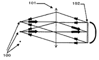
図15はベアチップタイプのLEDの配光分布を示した図であり、この図15に示すように、LED100の光出射方向中心から角度θをなすと、cosθに従ってθ方向の光強度が弱まることになる。
図16は、上記図15に示すような配光分布のLEDを用いた画像表示装置の構成を示した図であり、複数のLED100によりリレーレンズ101を介してライトバルブ102全体を照明すると、図示するようにLED100、100の配光分布が重畳され、ライトバルブ102上の照度ムラとなって現れてしまう。
このような特性はLEDにレンズをカップリングして形成される、いわゆる砲弾型LEDにおいても当然生じることになる。
そこで、このような光源(LED)の配光分布特性の問題を解決する方法としては、一般に蝿の目レンズを用いて光源の光束を複数に分割するようにしている。
しかしながら、蝿の目レンズを各LEDにカップリングさせる方法は現実的でなく、たとえカップリングさせたとしても、蝿の目レンズを構成する各レンズサイズは極めて小型となり、リレーレンズ系のアフォーカル倍率によってライトバルブ全面を蝿の目レンズ内の各レンズが形成する2次光源によって照明しようとすると、照明系の光軸方向が極めて大きくなってしまう。
また、各LEDから少しでも多くの光量をライトバルブに導こうとすると、必然的にLEDからライトバルブに光を導くリレーレンズ系のFナンバが明るくなり、レンズ径の大型化、収差補正のためのレンズ枚数増加を招くという欠点もあった。
そこで、本発明は上記したような点を鑑みてなされたものであり、ライトバルブの照度ムラを軽減し、リレーレンズ系のFナンバが暗くても明るく照明することができる画像表示装置と、そのような画像表示装置を備えたプロジェクタ及び画像観察装置を提供することを目的とする。
However, LEDs generally have different light intensity distributions for each emission angle, generally referred to as light distribution. In the case of a bare chip type LED, the light distribution is normally a distribution called Lambert.
FIG. 15 is a diagram showing a light distribution of a bare chip type LED. As shown in FIG. 15, when the angle θ is formed from the center of the light emitting direction of the
FIG. 16 is a diagram illustrating a configuration of an image display device using LEDs having a light distribution as shown in FIG. 15. When the
Such a characteristic naturally occurs also in a so-called bullet-type LED formed by coupling a lens to the LED.
Therefore, as a method for solving such a problem of the light distribution characteristics of the light source (LED), a light beam of the light source is generally divided into a plurality of light by using an eyelet lens.
However, the method of coupling the eyelet lens to each LED is not realistic, and even if it is coupled, the size of each lens constituting the eyelet lens is extremely small, and the afocal magnification of the relay lens system Therefore, if the entire surface of the light valve is illuminated by the secondary light source formed by each lens in the eyelet lens, the optical axis direction of the illumination system becomes extremely large.
Also, if you try to guide as much light as possible from each LED to the light valve, the F number of the relay lens system that inevitably guides the light from the LED to the light valve will become brighter, increasing the lens diameter and correcting aberrations. There was also a disadvantage that the number of lenses increased.
Accordingly, the present invention has been made in view of the above points, and an image display device capable of reducing illumination unevenness of a light valve and illuminating brightly even when the F number of a relay lens system is dark, and its It is an object of the present invention to provide a projector and an image observation apparatus provided with such an image display device.
上記目的を達成するため、請求項1記載の発明は、発光ダイオードとリレーレンズとライトバルブとを有し、前記発光ダイオードからの光を前記リレーレンズを介して前記ライトバルブに照射する画像表示装置において、前記発光ダイオードと前記リレーレンズの間に二次光源形成プリズムを備え、前記二次光源形成プリズムは、相対する二つの矩形面と少なくとも四つの多角形面とからなり、前記二つの矩形面のうち前記発光ダイオード側に位置する第一矩形面の面積が前記ライトバルブ側に位置する第二矩形面の面積より大きく、当該二次光源形成プリズムにより前記発光ダイオードの出射光束を複数に分割することを特徴とする。
また請求項2記載の発明は、請求項1に記載の画像表示装置において、前記二次光源形成プリズムにより前記発光ダイオードの出射光束が少なくとも5つに分割されることを特徴とする。
また請求項3記載の発明は、請求項1、2のいずれか一項に記載の画像表示装置において、前記二次光源形成プリズムの前記第一矩形面と前記第二矩形面は互いに平行になるように配置されていることを特徴とする。
また請求項4記載の発明は、請求項1、2のいずれか一項に記載の画像表示装置において、前記二次光源形成プリズムの前記第一矩形面と前記第二矩形面の形状は平面であることを特徴とする。
また請求項5記載の発明は、請求項1、2のいずれか一項に記載の画像表示装置において、前記二次光源形成プリズムの前記第一矩形面の形状は平面であり、前記第二矩形面の形状は曲面であることを特徴とする。
In order to achieve the above object, an image display device according to
According to a second aspect of the present invention, in the image display device according to the first aspect, the light emitted from the light emitting diode is divided into at least five by the secondary light source forming prism.
According to a third aspect of the present invention, in the image display device according to any one of the first and second aspects, the first rectangular surface and the second rectangular surface of the secondary light source forming prism are parallel to each other. It is arranged so that it may be arranged.
According to a fourth aspect of the present invention, in the image display device according to any one of the first and second aspects, the first rectangular surface and the second rectangular surface of the secondary light source forming prism are flat. It is characterized by being.
According to a fifth aspect of the present invention, in the image display device according to any one of the first and second aspects, the shape of the first rectangular surface of the secondary light source forming prism is a plane, and the second rectangular shape The shape of the surface is a curved surface.
また請求項6記載の発明は、請求項1に記載の画像表示装置において、前記二次光源形成プリズムは、前記第二矩形面のアスペクト比が前記ライトバルブのアスペクト比と等しいことを特徴とする。
また請求項7記載の発明は、請求項1に記載の画像表示装置において、前記二次光源形成プリズムは、前記多角形面の形状が台形または矩形であることを特徴とする。
According to a sixth aspect of the present invention, in the image display device according to the first aspect, the secondary light source forming prism has an aspect ratio of the second rectangular surface equal to an aspect ratio of the light valve. .
According to a seventh aspect of the present invention, in the image display device according to the first aspect, the secondary light source forming prism is characterized in that the polygonal surface has a trapezoidal shape or a rectangular shape .
また請求項8記載の発明は、請求項1乃至請求項7の何れか一項に記載の画像表示装置において、前記発光ダイオードは砲弾型発光ダイオードであることを特徴とする。
また請求項9記載の発明は、請求項1乃至請求項7の何れか一項に記載の画像表示装置において、前記発光ダイオードは反射型発光ダイオードであることを特徴とする。
また請求項10記載の発明は、請求項1乃至請求項7の何れか一項に記載の画像表示装置において、前記発光ダイオードと前記二次光源形成プリズムはそれぞれ一対一で対応する一組のユニットにより構成され、該ユニットを複数個並べて配置することで光源部が形成されることを特徴とする。
また請求項11記載の発明は、請求項10に記載の画像表示装置において、前記光源部は、少なくとも赤色、緑色、青色の発光ダイオードをそれぞれ一つずつ有することを特徴とする。
また請求項12記載の発明は、請求項11に記載の画像表示装置において、前記光源部はクロスダイクロイックプリズムを備えることを特徴とする。
また請求項13記載の発明は、請求項1乃至請求項12の何れか一項に記載の画像表示装置と投射光学系とを備えて構成されることを特徴とする。
また請求項14記載の発明は、請求項1乃至請求項12の何れか一項に記載の画像表示装置と接眼光学系とを備えて構成されることを特徴とする。
According to an eighth aspect of the present invention, in the image display device according to any one of the first to seventh aspects, the light emitting diode is a bullet type light emitting diode.
According to a ninth aspect of the present invention, in the image display device according to any one of the first to seventh aspects, the light emitting diode is a reflective light emitting diode.
According to a tenth aspect of the present invention, in the image display device according to any one of the first to seventh aspects, the light emitting diodes and the secondary light source forming prisms correspond to each other one-to-one. The light source section is formed by arranging a plurality of the units side by side.
According to an eleventh aspect of the present invention, in the image display device according to the tenth aspect , the light source section includes at least one red, green, and blue light emitting diodes.
According to a twelfth aspect of the present invention, in the image display device according to the eleventh aspect , the light source section includes a cross dichroic prism.
A thirteenth aspect of the invention includes the image display device according to any one of the first to twelfth aspects and a projection optical system.
The invention according to claim 14 is characterized by comprising the image display device according to any one of
以上説明したように、本発明の画像表示装置は、発光ダイオードとリレーレンズとの間に、相対する二つの矩形面と少なくとも四つの多角形面とからなり、二つの矩形面のうち、発光ダイオード側に位置する第一矩形面の面積を、ライトバルブ側に位置する第二矩形面の面積より大きく形成した2次光源形成プリズムを配置するようにしている。
そして、2次光源形成プリズムを各発光ダイオードにカップリングさせ、各発光ダイオードの出射光束を複数(少なくとも5つ)に分割することにより、発光ダイオードの配光分布特性の照度ムラに対する影響を低減することができる。
また本発明のように2次光源形成プリズムを用いるようにすると、従来に比べて光利用効率を高める事ができるため、発光ダイオードからの光取り出し効率の高い、即ち明るい画像表示装置を実現することができる。
また、従来に比べてリレーレンズのFナンバを暗くすることができるので、リレーレンズを小型でしかも少ない枚数で実現することができる。
As described above, the image display device of the present invention includes two opposing rectangular surfaces and at least four polygonal surfaces between the light emitting diode and the relay lens. A secondary light source forming prism is formed so that the area of the first rectangular surface located on the side is larger than the area of the second rectangular surface located on the light valve side.
Then, by coupling the secondary light source forming prism to each light emitting diode and dividing the emitted light beam of each light emitting diode into a plurality (at least five), the influence of the light distribution characteristics of the light emitting diode on the illuminance unevenness is reduced. be able to.
In addition, when the secondary light source forming prism is used as in the present invention, the light utilization efficiency can be increased as compared with the conventional case, so that an image display device with high light extraction efficiency from the light emitting diode, that is, a bright image display device is realized. Can do.
Further, since the F number of the relay lens can be made darker than in the prior art, the relay lens can be realized in a small size and with a small number of sheets.
以下、図面を参照しながら本発明の実施の形態について説明するが、本実施の形態についての説明を行う前にLEDを利用した画像表示装置の基本的な構成について説明する。
図1はLEDを利用した画像表示装置の基本的な構成を示した図である。
この図1に示す画像表示装置は、点光源である発光ダイオード(LED)1、リレーレンズ2、ライトバルブ3とにより構成される。LED1は例えば反射型の発光ダイオードであり、その配光分布は中心から角度一度ごとに1%光強度落ちるものとする。またリレーレンズ2は理想レンズとしてそのFナンバはF1.87とする。またライトバルブ3はアスペクト比1:1の正方形でその大きさは任意とする。
このように構成される画像表示装置では、LED1とライトバルブ3の中心を結ぶ直線を光軸aとし、光軸aを含みライトバルブ3の辺に垂直な平面において、リレーレンズ2の焦点にLED1を配置する照明系を考察すると、リレーレンズ2によってライトバルブ3に導かれる光束の最大立体角θは約30度であり、この時ライトバルブ3上における照度ムラはライトバルブ3の中心Rと最周辺P、Tとでは15%になる。つまり、ライトバルブ3の周辺P、Tではライトバルブ3の中心の約85%になる。なお、本来はライトバルブ3の対角長方向に最大立体角が対応するように設定するが、理解の容易さのために辺方向に最大立体角が対応するものとする。
Hereinafter, embodiments of the present invention will be described with reference to the drawings, but a basic configuration of an image display apparatus using LEDs will be described before the description of the present embodiment.
FIG. 1 is a diagram showing a basic configuration of an image display device using LEDs.
The image display apparatus shown in FIG. 1 includes a light emitting diode (LED) 1 that is a point light source, a
In the image display device configured as described above, a straight line connecting the center of the
以下、本実施の形態としての画像表示装置について説明する。
図2は、本発明の画像表示装置の第1実施形態としての2次光源形成プリズムの構造を示した図である。
この図2に示す2次光源形成プリズム10は、二つの矩形面、すなわち第一矩形面11と第二矩形面12と四つの台形面からなる。なお、本実施の形態では、図1に示したライトバルブ3のアスペクト比が1:1とされるので2次光源形成プリズム10の矩形面を正方形として説明するが、その形状はライトバルブ3のアスペクト比に応じて任意に設定可能である。
図3は、上記2次光源形成プリズムを利用したLED部の構成を示した図である。
この図3に示すLED部は、図2に示した2次光源形成プリズム10と、図1に示したような点光源であるLED1の近傍に配置することにより構成される。この場合、図3に示すように、2次光源形成プリズム10によって、LED1から出射される立体角30度の光束を光束A、O、Bに3分割することができる。さらに2次光源形成プリズム10の台形面13を通過する光束に着目すると、図のような位置に光源であるLED1の虚像LED1a、1bができることがわかる。本実施の形態では、このLED1の虚像1a、1bのことを2次光源と呼ぶこととする。なお、図2に示す2次光源形成プリズム10は台形面が4つあるので光束を5つに分割することが可能となる。また、各2次光源1a、1bは光軸方向の位置が本来の光源1の位置と多少異なるが、大きく問題になるものでなく、後述するように、2次光源形成プリズム10の矩形面12を曲面にすることで位置合わせは可能である。
Hereinafter, the image display apparatus according to the present embodiment will be described.
FIG. 2 is a diagram showing the structure of a secondary light source forming prism as the first embodiment of the image display device of the present invention.
The secondary light
FIG. 3 is a diagram illustrating a configuration of an LED unit using the secondary light source forming prism.
The LED section shown in FIG. 3 is configured by being arranged in the vicinity of the secondary light
図4は、本発明の画像表示装置の第1実施形態を示した図であり、この図4に示す画像表示装置は、LED1、2次光源形成プリズム10、リレーレンズ2、ライトバルブ3により構成される。LED1の配光分布は、上記同様、中心から角度一度ごとに1%光強度落ちるものとする。2次光源形成プリズム10の材料としてはd線の屈折率nd=1.517とする。リレーレンズ2は理想レンズとしてそのFナンバはF1.87、ライトバルブ3はアスペクト比1:1の正方形でその大きさは任意とする。
このように構成される本実施の形態の画像表示装置におけるライトバルブ3上での照度分布について考察すると、LED1出射光の中心方向の強度を100とし、ライトバルブ3を図示するように五分割(P、Q、R、S、T)して各点P、Q、R、S、Tの照度をプロットすると、
中心の光束Cが作る照度分布は、

光束Aが作る照度分布は
さらに光束Bが作る照度分布は、
Considering the illuminance distribution on the
The illuminance distribution created by the central luminous flux C is
The illuminance distribution created by the luminous flux A is
Furthermore, the illuminance distribution created by the luminous flux B is
このように画像表示装置を構成すれば照度ムラは、ライトバルブ3の中心位置Rと、その周辺位置Q、Rで1%、中心位置Rと端部P、Tでは2%弱まで低減することができる。なお、この照度ムラについての計算内容は、図4とは垂直な平面においても同様に成り立つ事は言うまでもない。
また、2次光源形成プリズム10を用いるようにすると、従来に比べて光利用効率を高める事ができるため、従来に比べてリレーレンズ2のFナンバを暗くすることができる。つまり、FナンバをF1.87からF5.71まで下げることが可能になり、リレーレンズ2を小型でしかも少ない枚数で実現することができるようになる。
また、2次光源形成プリズム10の多角形面(台形面)が矩形面となす角度について、例えばリレーレンズ2を光源側にテレセントリックにした場合には、多角形面から出射する光束の中心を通る光線が光軸と平行に出射するように設定すると光束を照明に十分利用できて望ましい。
そこで、本実施の形態では、図5に示すように2次光源形成プリズム10の台形面13出射する光束a、b、cの中心を通る光線がプリズム内部で光軸に対してなす角をαとし、台形面13が光軸となす角βとすると、
nd×sin{(90−β)−α}/sin(90−β)=1
という関係式から、α≒6.6、β≒71(度)となる。
このように2次光源形成プリズム10の多角形面13が矩形面11となす角度は、リレーレンズ2の軸外特性とマッチングさせることが望ましい。
If the image display device is configured in this way, the illuminance unevenness is reduced to 1% at the center position R of the
Further, if the secondary light
Further, regarding the angle between the polygonal surface (trapezoidal surface) of the secondary light
Therefore, in the present embodiment, as shown in FIG. 5, the angle formed by the light beam passing through the center of the light beams a, b, and c emitted from the
nd × sin {(90−β) −α} / sin (90−β) = 1
From the relational expression, α≈6.6 and β≈71 (degrees).
Thus, it is desirable to match the angle formed by the
なお、このような本実施の形態の2次光源形成プリズム10と類似の技術としては、先に述べた特許文献4、5が提案されているが、特許文献4に記載のプリズムは、直視型の有機ELディスプレイを対象としたものであり、直視型のため各画素からの画像表示用の光を正面方向に効率良く取り出すことのみを目的としている、これに対して本実施の形態のプリズムは照明用の光を対象としており、照度ムラを減らすために少なくとも4つ以上の多角形面がプリズムには必要であり、さらにライトバルブに導光するために、リレーレンズ2を必要としていることから特許文献4とは目的及び構成が明らかに異なるものである。また特許文献5のプリズムもその目的が明らかに異なるため矩形面を必要とせず、その構成が明らかに異なるものである。
なお、上記した例では、図4に示した2次光源形成プリズム10の多角形面から出射する光束の中心を通る光線が光軸となす角度は平行に限定されるものでなく、例えば2次光源形成プリズム10の側面を多角形面ではなく円筒のような曲率を有する面により構成することもできる。但し、図4に示した平面以外においては側面が曲率を有し、2次光源の位置ずれが発生するため望ましいものではない。
As techniques similar to the secondary light
In the above example, the angle formed by the light beam passing through the center of the light beam emitted from the polygonal surface of the secondary light
次に本発明の画像表示装置の第2実施形態について説明する。
第2の実施形態に係る画像表示装置は、第1の実施形態施と同じ配光分布のLEDの出射光束の立体角θを30度から60度まで取り込んだ場合の照度分布を示すものである。
図6は2次光源形成プリズムを配置しない場合の画像表示装置の構成を示した図、図7は2次光源形成プリズムを配置した場合の画像表示装置の構成を示した図である。この場合、2次光源形成プリズム20の台形の光軸となす角度が、上記第1の実施形態に比べてきつくなった分、光線追跡を行うと光束の端部の光線A、Bがライトバルブ3に入りきらずにロスとなるが、大きな影響は無いので、図7に示すように、この影響を無視して2次光源1a、1bからの光が全てライトバルブ3に入るものとし、第1の実施形態と同じ計算をすると、
中心の光束Cが作る照度分布は、
また光束Aが作る照度分布は、
さらに光束Bが作る照度分布は
従って、これらを足し合わせるとライトバルブ上の照度分布は
The image display apparatus according to the second embodiment shows the illuminance distribution when the solid angle θ of the emitted light beam of the LED having the same light distribution as in the first embodiment is taken from 30 degrees to 60 degrees. .
FIG. 6 is a diagram showing a configuration of the image display device when the secondary light source forming prism is not arranged, and FIG. 7 is a diagram showing a configuration of the image display device when the secondary light source forming prism is arranged. In this case, when the ray tracing is carried out by the amount that the angle formed by the trapezoidal optical axis of the secondary light
The illuminance distribution created by the central luminous flux C is
The illuminance distribution created by the luminous flux A is
Furthermore, the illuminance distribution created by the light beam B is
Therefore, when these are added together, the illuminance distribution on the light valve is
次に、本発明の画像表示装置の第3実施形態について説明する。
図8は第3の実施形態として2次光源形成プリズムを利用したLED部の構成を示した図である。
この図8に示す2次光源形成プリズム30は、出射側となる第二矩形面31を曲面により構成している。この場合、図8に示すように2次光源形成プリズム30の台形面32を通過した光束の光軸方向の2次光源位置1a、1bに中心光束の光源の虚像を合わせたものであり、第1の実施形態において説明してLED部より望ましい構成である。
図9は、本発明の画像表示装置を適用したカラー画像表示装置の構成を示した図である。
この図9に示すカラー画像表示装置は、赤色LED41R、緑色LED41G、青色LED41Bと、各々のLED41R、41G、41Bに対応して設けられ、二つの正方形面と四つの台形面からなる2次光源形成プリズム42、42、42と、光源側にテレセントリックな理想レンズである2枚のリレーレンズ43a、43b、アスペクト比が4:3とされるライトバルブ44によって構成される。
このように構成されるカラー画像表示装置においては、赤色、緑色、青色のLED41R、41G、41Bを時分割でオン・オフすることでカラー表示するものであり、一般にフィールドシーケンシャルと呼ばれているものである。
この場合、2次光源形成プリズム42の各面の大きさと、ライトバルブ44のアスペクト比関係について、2次光源形成プリズム42の第二矩形面42aから出射される中心の光束は、ライトバルブ44と対応しているので、同じアスペクト比であることが望ましい。多角形面42bの大きさは、アスペクト比よりも分割された光束がライトバルブ44全体を十分に照明できているかが重要であり、その大きさがライトバルブ44に入射する光束をけるものでなければ良い。図示しないが、例えば二次光源形成プリズム42は第一矩形面中心と第二矩形面中心を結ぶ直線を光軸とし、第二矩形面の短辺あるいは長辺に垂直で光軸を含む平面内で、LED1から出射する光束で第二矩形面から出射される光束の立体角(全角)を2φとすると、LED1から出射して二次光源形成プリズム42の第一矩形面に入射する光束で二次光源形成プリズム42の多角形面から出射する光束の立体角は、少なくとも2φ以上にしておく必要がある。
2次光源形成プリズム42の多角形面が矩形面となす角度は、第1の実施形態において多角形面42bから出射される光束の中心を通る光線が光軸に対して平行に出射するように設定したため、リレーレンズ43a、43bを光源側にテレセントリックにすれば、本実施形態のようにLED41と二次光源形成プリズム42の光源ユニットを平面上に配列した場合にも、各光源41からの出射光を十分に利用することができる。
このように2次光源形成プリズム42の多角形面42bが矩形面42aとなす角度は、光源ユニットを平面配列することを想定すると、多角形面42bから出射される光束の中心を通る光線が光軸に対して平行に出射するように設定することが望ましく、なおかつこのとき光源側にテレセントリックなリレーレンズを組み合わせることが望ましい。
図10は、上記図9に示したカラー画像表示装置であるプロジェクタの具体的な構成を示した図である。
この図10に示すように偏光変換作用を持ったPBS45と、反射型液晶46、投射レンズ47を配置することでプロジェクタを構成することができる。
Next, a third embodiment of the image display device of the present invention will be described.
FIG. 8 is a diagram showing a configuration of an LED unit using a secondary light source forming prism as the third embodiment.
In the secondary light source forming prism 30 shown in FIG. 8, the second
FIG. 9 is a diagram showing a configuration of a color image display device to which the image display device of the present invention is applied.
The color image display device shown in FIG. 9 is provided with a
In the color image display device configured as described above, the red, green, and
In this case, with respect to the size of each surface of the secondary light
The angle formed by the polygonal surface of the secondary light
As described above, assuming that the
FIG. 10 is a diagram showing a specific configuration of the projector which is the color image display device shown in FIG.
As shown in FIG. 10, a
次に第4の実施形態としての画像表示装置について説明する。
図11は第4の実施形態としてのLED部の構成を示した図である。
この図11に示すLED部は、図3に示したLED部のLED1と2次光源形成プリズム10との間にカップリングレンズ51を配置したものである。LED1にカップリングレンズ51を配置したものは、砲弾型LEDとして知られており、2次光源形成プリズム10の組み合わせ例である。図11に示すように、砲弾型LEDを用いても2次光源形成プリズム10の使い方に何ら変化なく利用することができる。
次に、第5の実施形態としての画像表示装置について説明する。
図12は第5の実施形態としての画像表示装置に適用されるLED部の構成を示した図であり、この図12に示す2次光源形成プリズム61の多角形面を8面に増やしたものであり、図12は光軸を含み第1矩形面61aと第2矩形面61bに垂直な平面にLED1から出射される立体角50度の光束を各10度の光束O、A、B、C、Dに分割することができる。
図13は、上記図12に示した本発明の画像表示装置の第1実施形態を示した図である。
この図13に示す画像表示装置は、LED1、2次光源形成プリズム61、リレーレンズ2、ライトバルブ3により構成される。このように構成される本実施の形態の画像表示装置によれば、2次光源形成プリズム61の多角形面を増やすと、一つ一つの光束の有する配光分布を小さくすることができ、より照度ムラを小さくすることができる。
また、図13に示すように50度という大きな光束を扱っても、各10度の光束に分割することができるので、2次光源形成プリズム61を用いるようにすると、従来に比べて光利用効率を高める事ができるため、従来に比べてリレーレンズ2のFナンバを暗くすることができる。つまり、FナンバをF1.87からF5.71まで下げることが可能になり、リレーレンズ2を小型でしかも少ない枚数で実現することができるようになる。
Next, an image display apparatus as a fourth embodiment will be described.
FIG. 11 is a diagram showing a configuration of an LED unit as the fourth embodiment.
The LED unit shown in FIG. 11 is obtained by arranging a
Next, an image display apparatus as a fifth embodiment will be described.
FIG. 12 is a diagram showing a configuration of an LED unit applied to the image display device as the fifth embodiment, and the polygonal surface of the secondary light
FIG. 13 is a diagram showing a first embodiment of the image display apparatus of the present invention shown in FIG.
The image display device shown in FIG. 13 includes an
Further, as shown in FIG. 13, even if a large luminous flux of 50 degrees is handled, it can be divided into luminous fluxes of 10 degrees. Therefore, if the secondary light
図14は、上記図13に示したカラー画像表示装置であるプロジェクタの具体的な構成を示した図である。なお、図10と同一部位には同一番号を付して説明は省略する。
この図14に示す赤色LED41R、緑色LED41G、青色LED41Bを時分割でオン・オフすることでカラー表示するものであり、赤色LED41R、緑色LED41G、青色のLED41Bを、それぞれクロスダイクロイックプリズム71に向かって複数個ずつ配列したものである。これは、LEDアレイの平面を大きくしていくと、リレーレンズの軸外性能を高める必要があり、また投射レンズ46のFナンバもどんどん明るくする必要が出てくることから、LEDアレイの平面の大型化は光学的には好ましくない。
そこで、図14に示すようにクロスプリズム71を用いることで、リレーレンズ43a、43bにとっては1平面と同じ性能でライトバルブ45に3倍の光束を導光することができるようになる。
なお、本実施の形態では、本発明の画像表示装置と投射光学系とを組み合わせてプロジェクタなどの画像表示装置を構成する場合を例にあげて説明したが、これはあくまでも一例であり、本発明の画像表示装置と接眼光学系とを組み合わせて画像観察装置を構成することも勿論可能である。
FIG. 14 is a diagram showing a specific configuration of the projector which is the color image display device shown in FIG. In addition, the same number is attached | subjected to the same site | part as FIG. 10, and description is abbreviate | omitted.
The
Therefore, by using the
In the present embodiment, the case where an image display device such as a projector is configured by combining the image display device of the present invention and a projection optical system has been described as an example. However, this is only an example, and the present invention is described. Of course, an image observation apparatus can be configured by combining the image display apparatus and the eyepiece optical system.
1、41 LED、1a、1b 2次光源位置、2、43a、43b リレーレンズ、3、44 ライトバルブ、10、30、42 2次光源形成プリズム、11 第一矩形面、12、31 第二矩形面、13、32 多角形面(台形面)、71 クロスダイクロイックプリズム 1, 41 LED, 1a, 1b Secondary light source position, 2, 43a, 43b Relay lens, 3, 44 Light valve, 10, 30, 42 Secondary light source forming prism, 11 First rectangular surface, 12, 31 Second rectangle Surface, 13, 32 Polygonal surface (trapezoidal surface), 71 Cross dichroic prism
Claims (14)
前記発光ダイオードと前記リレーレンズの間に二次光源形成プリズムを備え、
前記二次光源形成プリズムは、相対する二つの矩形面と少なくとも四つの多角形面とからなり、前記二つの矩形面のうち前記発光ダイオード側に位置する第一矩形面の面積が前記ライトバルブ側に位置する第二矩形面の面積より大きく、
当該二次光源形成プリズムにより前記発光ダイオードの出射光束を複数に分割することを特徴とする画像表示装置。 In an image display device having a light emitting diode, a relay lens, and a light valve, and irradiating the light valve with light from the light emitting diode through the relay lens,
A secondary light source forming prism is provided between the light emitting diode and the relay lens,
The secondary light source forming prism includes two opposing rectangular surfaces and at least four polygonal surfaces, and the area of the first rectangular surface located on the light emitting diode side of the two rectangular surfaces is the light valve side. Larger than the area of the second rectangular surface located at
An image display device, wherein the light emitted from the light emitting diode is divided into a plurality of light beams by the secondary light source forming prism.
Priority Applications (2)
| Application Number | Priority Date | Filing Date | Title |
|---|---|---|---|
| JP2004253052A JP4685386B2 (en) | 2004-08-31 | 2004-08-31 | Image display device, projector device, and image observation device |
| US11/200,289 US7527394B2 (en) | 2004-08-31 | 2005-08-10 | Image-displaying apparatus |
Applications Claiming Priority (1)
| Application Number | Priority Date | Filing Date | Title |
|---|---|---|---|
| JP2004253052A JP4685386B2 (en) | 2004-08-31 | 2004-08-31 | Image display device, projector device, and image observation device |
Publications (2)
| Publication Number | Publication Date |
|---|---|
| JP2006071817A JP2006071817A (en) | 2006-03-16 |
| JP4685386B2 true JP4685386B2 (en) | 2011-05-18 |
Family
ID=35942763
Family Applications (1)
| Application Number | Title | Priority Date | Filing Date |
|---|---|---|---|
| JP2004253052A Expired - Fee Related JP4685386B2 (en) | 2004-08-31 | 2004-08-31 | Image display device, projector device, and image observation device |
Country Status (2)
| Country | Link |
|---|---|
| US (1) | US7527394B2 (en) |
| JP (1) | JP4685386B2 (en) |
Families Citing this family (23)
| Publication number | Priority date | Publication date | Assignee | Title |
|---|---|---|---|---|
| JP2005140847A (en) * | 2003-11-04 | 2005-06-02 | Tamron Co Ltd | Led light source projector optical system and led light source projector |
| JP2007058163A (en) | 2005-07-27 | 2007-03-08 | Ricoh Co Ltd | Light source apparatus, optical modulation apparatus, display apparatus, light condensing lighting system and projection type color display apparatus |
| US7387389B2 (en) * | 2006-01-13 | 2008-06-17 | Hewlett-Packard Development Company, L.P. | Image display system and method |
| JP2007273506A (en) * | 2006-03-30 | 2007-10-18 | Sumitomo Chemical Co Ltd | Compound semiconductor light emitting device |
| JP5044992B2 (en) * | 2006-05-26 | 2012-10-10 | セイコーエプソン株式会社 | Light emitting element and projector |
| US7507942B2 (en) | 2006-06-13 | 2009-03-24 | Ricoh Company, Ltd. | Illumination apparatus that suppresses light intensity distribution irregularity and projection-type display apparatus using the illumination apparatus |
| JP2008032996A (en) | 2006-07-28 | 2008-02-14 | Ricoh Co Ltd | Original document illuminating device, image reader, color original reader, and image forming apparatus |
| JP2008072398A (en) * | 2006-09-13 | 2008-03-27 | Ricoh Co Ltd | Original illuminator, image reader, color original reader and image forming apparatus |
| US8614413B2 (en) * | 2007-01-31 | 2013-12-24 | Ricoh Company, Ltd. | Image reading apparatus to illuminate light on an original document with an optical member having four planes positioned such that the light incident side is smaller in size than the light exit side |
| KR100925720B1 (en) * | 2007-02-20 | 2009-11-10 | 재단법인대구경북과학기술원 | Projection display device with dual mode function |
| KR100939501B1 (en) * | 2007-02-20 | 2010-01-29 | 재단법인대구경북과학기술원 | Multimedia playback device that provides two projection images |
| US8081355B2 (en) * | 2007-03-05 | 2011-12-20 | Ricoh Company, Ltd. | Illumination unit, image read apparatus, image formation apparatus |
| JP5049147B2 (en) * | 2008-01-23 | 2012-10-17 | 株式会社リコー | Image reading apparatus and image forming apparatus |
| CN101988630B (en) * | 2009-07-31 | 2013-01-09 | 深圳市光峰光电技术有限公司 | Stage lighting system and method thereof for proving high-brightness white light |
| EP2296436B1 (en) * | 2009-09-07 | 2018-11-14 | Nxp B.V. | System and method for output flux measurement of a light emitting diode |
| TWI452739B (en) | 2010-10-20 | 2014-09-11 | Macroblock Inc | Light-emitting diode package structure and light-emitting diode stereoscopic display device |
| JP5605211B2 (en) | 2010-12-20 | 2014-10-15 | 株式会社リコー | Projection optical system and image projection apparatus |
| JP5621583B2 (en) | 2010-12-27 | 2014-11-12 | 株式会社リコー | Projection optical system and image projection apparatus |
| EP2560393B1 (en) | 2011-08-16 | 2018-10-10 | Ricoh Company Ltd. | Image displaying apparatus |
| JP2017044870A (en) | 2015-08-26 | 2017-03-02 | 株式会社リコー | Image display device and image display unit |
| JP6604090B2 (en) | 2015-08-27 | 2019-11-13 | 株式会社リコー | Projection optical system, projection apparatus and projection system |
| KR102667782B1 (en) * | 2016-10-31 | 2024-05-21 | 삼성전자주식회사 | Pannel apparatus displaying 3d image and display apparatus comprising the same |
| JP6806911B2 (en) * | 2017-09-04 | 2021-01-06 | 富士フイルム株式会社 | Backlight unit and liquid crystal display |
Citations (6)
| Publication number | Priority date | Publication date | Assignee | Title |
|---|---|---|---|---|
| JPH04136947U (en) * | 1991-06-14 | 1992-12-21 | 市光工業株式会社 | Automotive high mount stop lamp |
| JP2001042431A (en) * | 1999-07-30 | 2001-02-16 | Nitto Kogaku Kk | Light source device and projector device |
| JP2001249400A (en) * | 2000-03-03 | 2001-09-14 | Seiko Epson Corp | Projection display device |
| JP2004134803A (en) * | 2002-10-10 | 2004-04-30 | Agilent Technol Inc | Chip shape of flip-chip type light emitting diode |
| JP2004151173A (en) * | 2002-10-29 | 2004-05-27 | Nitto Kogaku Kk | Optical engine |
| JP2004212469A (en) * | 2002-12-27 | 2004-07-29 | Hayashi Soken:Kk | Illuminator and microscope using same |
Family Cites Families (16)
| Publication number | Priority date | Publication date | Assignee | Title |
|---|---|---|---|---|
| JP3257646B2 (en) | 1993-04-05 | 2002-02-18 | 富士ゼロックス株式会社 | Laser beam printer |
| GB9420750D0 (en) * | 1994-10-14 | 1994-11-30 | Philips Electronics Uk Ltd | Colour liquid crystal projection display systems |
| JPH09288203A (en) * | 1996-02-22 | 1997-11-04 | Nikon Corp | Multiple focal line lens |
| JP2001343706A (en) * | 2000-05-31 | 2001-12-14 | Sony Corp | Video display device |
| JP2002208386A (en) | 2001-01-05 | 2002-07-26 | Ricoh Co Ltd | Portable electronic equipment |
| JP2002244211A (en) | 2001-02-22 | 2002-08-30 | Ricoh Co Ltd | Image projection device |
| TW571119B (en) | 2001-12-20 | 2004-01-11 | Delta Electronics Inc | Image projection device with integrated semiconductor light emitting element light source |
| KR100453040B1 (en) * | 2002-02-01 | 2004-10-15 | 삼성전자주식회사 | Collimating lens, collimating system and image displaying apparatus employing the same |
| JP4289027B2 (en) * | 2002-07-25 | 2009-07-01 | 豊田合成株式会社 | Light emitting device |
| JP4111074B2 (en) * | 2002-08-20 | 2008-07-02 | セイコーエプソン株式会社 | projector |
| JP4032918B2 (en) | 2002-10-24 | 2008-01-16 | ソニー株式会社 | Display device and manufacturing method thereof |
| JP4416391B2 (en) | 2002-11-22 | 2010-02-17 | 株式会社リコー | Wide-angle lens, camera and projection display device |
| US7159987B2 (en) * | 2003-04-21 | 2007-01-09 | Seiko Epson Corporation | Display device, lighting device and projector |
| US7306344B2 (en) * | 2003-06-10 | 2007-12-11 | Abu-Ageel Nayef M | Light guide array, fabrication methods and optical system employing same |
| US7427146B2 (en) * | 2004-02-11 | 2008-09-23 | 3M Innovative Properties Company | Light-collecting illumination system |
| US7168810B2 (en) * | 2004-04-23 | 2007-01-30 | Infocus Corporation | Method and apparatus for arranging light emitting devices in projection systems |
-
2004
- 2004-08-31 JP JP2004253052A patent/JP4685386B2/en not_active Expired - Fee Related
-
2005
- 2005-08-10 US US11/200,289 patent/US7527394B2/en not_active Expired - Fee Related
Patent Citations (6)
| Publication number | Priority date | Publication date | Assignee | Title |
|---|---|---|---|---|
| JPH04136947U (en) * | 1991-06-14 | 1992-12-21 | 市光工業株式会社 | Automotive high mount stop lamp |
| JP2001042431A (en) * | 1999-07-30 | 2001-02-16 | Nitto Kogaku Kk | Light source device and projector device |
| JP2001249400A (en) * | 2000-03-03 | 2001-09-14 | Seiko Epson Corp | Projection display device |
| JP2004134803A (en) * | 2002-10-10 | 2004-04-30 | Agilent Technol Inc | Chip shape of flip-chip type light emitting diode |
| JP2004151173A (en) * | 2002-10-29 | 2004-05-27 | Nitto Kogaku Kk | Optical engine |
| JP2004212469A (en) * | 2002-12-27 | 2004-07-29 | Hayashi Soken:Kk | Illuminator and microscope using same |
Also Published As
| Publication number | Publication date |
|---|---|
| US20060044795A1 (en) | 2006-03-02 |
| JP2006071817A (en) | 2006-03-16 |
| US7527394B2 (en) | 2009-05-05 |
Similar Documents
| Publication | Publication Date | Title |
|---|---|---|
| JP4685386B2 (en) | Image display device, projector device, and image observation device | |
| US8500285B2 (en) | Projection type display apparatus | |
| JP4616577B2 (en) | Video display device | |
| US7589307B2 (en) | Image display apparatus that reduces illuminance irregularity, projection-type image display apparatus using the image display apparatus and rear-projection televison | |
| US20090231846A1 (en) | Illumination light source and image projector | |
| JP2005157059A (en) | Lighting device and projector | |
| JP2000180962A (en) | Projection illuminating device | |
| JP5403255B2 (en) | Lighting device and projector | |
| JP2004220016A (en) | Lighting system and projection-type image display | |
| JP2005116266A (en) | Lighting device, display device, and projector | |
| US20050213345A1 (en) | Light source device for illumination | |
| JP2006243603A (en) | Condensing element, lighting device, and projection image display device | |
| JP4909546B2 (en) | Illumination device, light modulation device, and projection display device | |
| JP2009063892A (en) | Projector, optical element, and light modulation device | |
| CN210109545U (en) | Self-luminous projection display system and micro-display full-color optical machine | |
| JP2007333856A (en) | Lighting system, light modulator, and projection display device | |
| JP2008070769A (en) | Light source unit, illumination device and projector device | |
| US20050213344A1 (en) | Light source device for illumination | |
| JP4807981B2 (en) | Image display device and projection optical system projector | |
| JP2005099468A (en) | Lighting device and projector | |
| JP2008032907A (en) | Image display device, projection type image display device, and rear projection television | |
| JP2007072172A (en) | Illumination device and projection-type display apparatus | |
| CN114265273A (en) | Light source device and projector | |
| JP4893780B2 (en) | LIGHTING DEVICE AND PROJECTOR HAVING THE SAME | |
| JP4581407B2 (en) | Light source unit and projection-type image display device using the same |
Legal Events
| Date | Code | Title | Description |
|---|---|---|---|
| A621 | Written request for application examination |
Free format text: JAPANESE INTERMEDIATE CODE: A621 Effective date: 20070326 |
|
| A131 | Notification of reasons for refusal |
Free format text: JAPANESE INTERMEDIATE CODE: A131 Effective date: 20100525 |
|
| A521 | Request for written amendment filed |
Free format text: JAPANESE INTERMEDIATE CODE: A523 Effective date: 20100721 |
|
| A131 | Notification of reasons for refusal |
Free format text: JAPANESE INTERMEDIATE CODE: A131 Effective date: 20101116 |
|
| A521 | Request for written amendment filed |
Free format text: JAPANESE INTERMEDIATE CODE: A523 Effective date: 20110107 |
|
| TRDD | Decision of grant or rejection written | ||
| A01 | Written decision to grant a patent or to grant a registration (utility model) |
Free format text: JAPANESE INTERMEDIATE CODE: A01 Effective date: 20110201 |
|
| A01 | Written decision to grant a patent or to grant a registration (utility model) |
Free format text: JAPANESE INTERMEDIATE CODE: A01 |
|
| A61 | First payment of annual fees (during grant procedure) |
Free format text: JAPANESE INTERMEDIATE CODE: A61 Effective date: 20110210 |
|
| FPAY | Renewal fee payment (event date is renewal date of database) |
Free format text: PAYMENT UNTIL: 20140218 Year of fee payment: 3 |
|
| R150 | Certificate of patent or registration of utility model |
Free format text: JAPANESE INTERMEDIATE CODE: R150 |
|
| LAPS | Cancellation because of no payment of annual fees |