JP4655321B2 - Heat treatment method - Google Patents
Heat treatment method Download PDFInfo
- Publication number
- JP4655321B2 JP4655321B2 JP2000013532A JP2000013532A JP4655321B2 JP 4655321 B2 JP4655321 B2 JP 4655321B2 JP 2000013532 A JP2000013532 A JP 2000013532A JP 2000013532 A JP2000013532 A JP 2000013532A JP 4655321 B2 JP4655321 B2 JP 4655321B2
- Authority
- JP
- Japan
- Prior art keywords
- temperature
- heat treatment
- film
- gas
- polysilicon film
- Prior art date
- Legal status (The legal status is an assumption and is not a legal conclusion. Google has not performed a legal analysis and makes no representation as to the accuracy of the status listed.)
- Expired - Fee Related
Links
Images


Classifications
-
- H—ELECTRICITY
- H10—SEMICONDUCTOR DEVICES; ELECTRIC SOLID-STATE DEVICES NOT OTHERWISE PROVIDED FOR
- H10D—INORGANIC ELECTRIC SEMICONDUCTOR DEVICES
- H10D1/00—Resistors, capacitors or inductors
- H10D1/60—Capacitors
- H10D1/68—Capacitors having no potential barriers
- H10D1/692—Electrodes
- H10D1/711—Electrodes having non-planar surfaces, e.g. formed by texturisation
- H10D1/712—Electrodes having non-planar surfaces, e.g. formed by texturisation being rough surfaces, e.g. using hemispherical grains
-
- H10P32/12—
-
- H10P32/171—
-
- H10P32/302—
-
- H—ELECTRICITY
- H10—SEMICONDUCTOR DEVICES; ELECTRIC SOLID-STATE DEVICES NOT OTHERWISE PROVIDED FOR
- H10B—ELECTRONIC MEMORY DEVICES
- H10B12/00—Dynamic random access memory [DRAM] devices
- H10B12/01—Manufacture or treatment
- H10B12/02—Manufacture or treatment for one transistor one-capacitor [1T-1C] memory cells
- H10B12/03—Making the capacitor or connections thereto
- H10B12/033—Making the capacitor or connections thereto the capacitor extending over the transistor
Landscapes
- Semiconductor Memories (AREA)
- Semiconductor Integrated Circuits (AREA)
- Chemical Vapour Deposition (AREA)
- Internal Circuitry In Semiconductor Integrated Circuit Devices (AREA)
- Formation Of Insulating Films (AREA)
Description
【0001】
【発明の属する技術分野】
本発明は、半導体ウエハ等を熱処理する熱処理方法に係り、特にキャパシタの電極の形成時に用いるのに適する熱処理方法に関する。
【0002】
【従来の技術】
一般に、IC等の半導体集積回路を形成するためには、半導体ウエハやガラス基板等の表面に、成膜処理、エッチング処理、熱拡散処理、酸化処理等を多数回繰り返し行なうことによって所望のトランジスタ素子、抵抗素子、キャパシタ等を高密度に集積形成するようになっている。
近年、特に、半導体装置の高集積化にともなって、各素子自体の微細化も一層進む傾向にある。例えばDRAM等の記憶装置にあっては各セルの占有面積は微細化傾向によって益々小さくなるが、十分な容量値を確保するためには、占有面積が小さくなってもキャパシタ電極間の絶縁層の厚さを薄くしたり、もしくはこの誘電体の比誘電率を大きくすればよいが、この絶縁層の厚さを薄くすると絶縁性が劣化し、また、材質を高誘電体とするにも種々の技術的な問題があるのが現状である。
【0003】
そこで、キャパシタの電極表面に、表面が微細に凹凸形状になされたポリシリコン膜を形成して微細な占有面積でも容量値に寄与する実質的な表面積を2〜3倍に増加させることが行なわれている。この表面凹凸形状のポリシリコン膜を形成するためには、例えば特開平5−304273号公報や特開平7−221034号公報等に開示されているように、ノンドープのアモルファスシリコン膜の表面にシリコン核結晶を成長させて凹凸形状のHSG(Hemispherical Grained)ポリシリコン膜を選択的に形成する方法や、ある特定の成膜条件中に設定することより、ウエハ表面全体に直接的に凹凸形状のラグド(Rugged)ポリシリコン膜を堆積して、これを選択エッチングすることにより特定の部位のみにポリシリコン膜を形成する方法が知られている。
【0004】
ここで、キャパシタの電極等の所望の部位にHSGポリシリコン膜やラグドポリシリコン膜のような表面凹凸形状のポリシリコン膜を形成する方法を簡単に説明する。
図9は、表面凹凸形状のポリシリコン膜としてHSGポリシリコン膜を形成するための工程図である。図9(A)において、例えばシリコン基板よりなる半導体ウエハWの表面には、チャネルストッパ2、ソース4及びドレイン6が形成され、これらの表面には例えばTEOS等を用いて成膜されたSiO2 よりなる層間絶縁膜8が形成される。上記ソース4及びドレイン6間の層間絶縁膜8には、ゲート電極10が埋め込まれ、また、ドレイン6には、ビットライン12が接続されている。また、上記ソース4には、層間絶縁膜8を貫通したコンタクトホールを埋め込むようにして形成された下部電極14が接続されており、この下部電極14の上端は、円筒リング状に形成されて、いわゆるスタックキャパシタを製造できるようになっている。この下部電極14は、例えばリン原子がドープされた、リンドープアモルファスシリコン膜により形成される。
【0005】
さて、このように図9(A)のように形成された半導体ウエハWは、次に図9(B)に示すようにその下部電極14の表面にノンドープアモルファスシリコン膜16が選択的に形成され、更に、高真空下の熱処理でマイグレーションを生ぜしめることにより、シリコンの核結晶をノンドープアモルファスシリコン膜16上のみに選択的に形成し、更にノンドープアモルファスシリコン膜16の原子が動くことにより上記核結晶を図9(C)に示すように成長させて表面に凹凸のあるHSGシリコン膜18を形成する。この時、プロセスガスはシランやジシランを用い、プロセス温度は例えば500〜600℃程度、プロセス圧力は例えばシランを用いた時の分圧は2×10⁻³Torr(2.66×10⁻¹Pa)以下である。
【0006】
また、図10は、表面凹凸形状のポリシリコン膜としてラグドポリシリコン膜を形成するための工程図である。図10(A)は、先に図9(A)に示したと同じ状態であり、このような状態で、所定の成膜処理により、図10(B)に示すように、ウエハWの表面全体に直接的に表面が凹凸状のラグドポリシリコン膜20を堆積させる。この場合、ウエハ表面全面にラグドポリシリコン膜20が堆積するので、その後、パターンエッチングにより、図10(C)に示すように下部電極14の表面のラグドポリシリコン膜20のみを残して不要な部分のラグドポリシリコン膜を除去する。
【0007】
さて、図9及び図10に示すように、下部電極14の表面に凹凸形状のHSGポリシリコン膜18や凹凸形状のラグドポリシリコン膜20を形成したならば、次に、所定の温度でアニール処理を行なうことにより、下層のリンドープアモルファスシリコン膜の下部電極14からリン原子を上記核ポリシリコン膜18、20へ拡散させて、これを下部電極の一部とする。これにより、下部電極14の表面積を、上述のようにリンがドープされたポリシリコン膜18、20の表面の凹凸により実質的に拡大することが可能となる。
その後は、図11に示すように、下部電極14の表面側に、SiO2 等よりなる容量絶縁膜22を形成し、更にパターニングされた上部電極24を形成することによりキャパシタを製造する。
【0008】
【発明が解決しようとする課題】
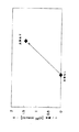
ところで、HSGポリシリコン膜18やラグドポリシリコン膜20を下部電極の一部として十分に機能させるためには、下層のリンドープのアモルファスシリコン膜の下部電極14から十分な量のリン原子を拡散によりドープする必要があるが、このリン原子の拡散が十分に行なわれずに、容量低下の原因となる空乏層が発生する場合がある。この時の状態は、図12に示されている。図12は上述のように製造されたキャパシタに+と−の電圧を印加した時の容量の変化を示すグラフである。このグラフから明らかなように、特に電圧をマイナス(−)方向に振った時に容量が大幅に低下しており、特性上好ましくない。
【0009】
この対策として、HSGポリシリコン膜の場合は、この膜厚を薄くすることも考えられるが、膜厚が薄過ぎるとHSG表面の凹凸ができなくなる。また、下地の下部電極14のリン濃度を高くすることも考えられるが、リン濃度が高過ぎるとマイグレーションによるHSGを形成し難くなるという問題がある。
その他の対策として、シリコン膜18、20中に、インプラテーション装置により、リン原子を直接的に打ち込むことも行なわれているが、この場合には、イオン打ち込みによるダメージをかなり受けるのみならず、図9及び図10に示すような複雑な形状の下部電極14では例えば側壁部分へのイオンの回り込みが難しくなって、均一なイオン濃度で打ち込みが困難になるという問題があった。
【0010】
更には、POCl3 雰囲気中でアニール処理することにより、ポリシリコン膜18、20中にリン原子をドープさせることも行なわれているが、この場合にはアニール温度を800℃以上に設定しなければリンが十分にドープされないが、このような高温状態に半導体ウエハ自体を曝すと、サーマルバジェットにより深さ方向にリン濃度が変動し、素子の設計値から外れてしまうという問題があった。
本発明は、以上のような問題点に着目し、これを有効に解決すべく創案されたものである。本発明の目的は、表面凹凸形状のポリシリコン膜にリン原子を効率的にドーピングして空乏層の発生を抑制することができる熱処理方法を提供することにある。
【0011】
【課題を解決するための手段】
請求項1に規定する発明は、表面が微細な凹凸形状になされたシリコン膜が選択的に形成されている被処理体を熱処理装置の処理容器内へロードして、所定のプロセス温度で前記シリコン膜中に不純物としてリン原子を導入する熱処理方法において、前記被処理体を前記プロセス温度より低い温度の前記処理容器内へロードするローディング工程と、前記処理容器の温度を前記プロセス温度まで昇温すると共に前記昇温の全期間においてN 2 ガスを前記処理容器内へ供給する昇温工程と、記N 2 ガスの供給を停止し、前記リン原子のドーピングガスとしてPH 3 ガスの供給を開始すると共に熱処理温度を550〜750℃の範囲内に維持してリン原子のドープを行なうアニール工程と、を有するようにした。
このように、ドーピングガスとしてPH3 ガスを用い、しかも、熱処理温度を550〜750℃の範囲内に設定することにより、温度が750℃よりも低いので、不純物濃度が設計値よりも大きく変動することもなく、また、温度が550℃以上なので、不純物のドープの効率もある程度高く維持することが可能となる。
【0012】
この場合、請求項2に規定するように、例えば前記被処理体を前記処理容器内へロードする際には、前記処理容器の温度を400℃より低い温度に設定することにより、被処理体のシリコン膜に付着する自然酸化膜を抑制することが可能となる。
また本発明の関連技術として、例えば前記処理容器内にロードされた前記被処理体を、昇温前にサイクルパージ処理に晒すことにより、例えば被処理体の絶縁層等に含まれる水分やガス等を事前に排出させることができ、熱処理時に自然酸化膜が付着することを防止することが可能となる。
【0013】
更に、本発明の関連技術として、例えば前記被処理体を熱処理温度まで昇温する際には、前記処理容器内は昇温前に所定の圧力で前記ドーピングガスにより満たされているようにすることにより、ポリシリコン膜の再マイグレーションが発生してその表面積が減少することを防止することが可能となる。
また、請求項3に規定するように、例えば前記熱処理時には、プロセス圧力を100〜400Torrの範囲内に維持することにより、リン原子のドーピング効率を向上させることが可能となる。
【0014】
また、本発明の関連技術として、例えば前記ドーピングガスの供給は、熱処理時に前記被処理体を所定の温度以下に降温させるまで継続して行なうことにより前記処理容器内を所定の圧力に維持する。これにより、ポリシリコン膜の再マイグレーションが発生してその表面積が減少することを防止することが可能となる。
また、請求項4に規定するように、例えば前記表面が凹凸形状になされたシリコン膜は、HSGポリシリコン膜或いはラグド(Rugged)ポリシリコン膜により形成する。
【0015】
また、請求項5に規定するように、例えば前記リン原子が導入されたシリコン膜は、キャパシタの電極の一部を構成する。
【0016】
【発明の実施の形態】
以下に、本発明に係る熱処理方法の一実施例を添付図面に基づいて詳述する。
図1は本発明方法を実施するための熱処理装置の一例を示す概略構成図、図2は本発明方法の第1実施例を説明するためのタイムチャート図である。
図示するように、この熱処理装置30は、複数の被処理体である例えばシリコン基板よりなる半導体ウエハWを一度に熱処理する縦型の熱処理部32と、この下方に設けられて半導体ウエハWの搬入搬出を行なう搬出入部34とにより構成されている。
上記熱処理部32は、例えば耐熱性の石英により形成された処理容器36を有しており、この処理容器36は、下端が開放された有天井の外筒38とこの内側に所定の間隔を隔てて同心状に配置された円筒体状の内筒40により構成されて2重管構造になされている。この外筒38の外側には、加熱ヒータ42を配置して全体として加熱炉を形成しており、内部に収容される半導体ウエハを所定の温度に加熱し得るようになっている。
【0017】
この処理容器36の下部側壁には、上記外筒38と内筒40との間に処理ガスを導入するためのガス導入ノズル44及び内筒40側から処理容器36内の雰囲気を真空引きするための排気ノズル46がそれぞれ設けられている。
25〜150枚程度の半導体ウエハWは、例えば石英製のウエハボート48に上下方向に多段に略等ピッチで支持されており、このウエハボート48は、搬出入部34内に収容されている、例えばボールネジ等よりなる昇降機構50により昇降される支持アーム52の先端に支持されている。具体的には、支持アーム52の先端には、上記処理容器36の下端開口部を気密にシールする円板状のキャップ部54を設け、この上に、例えば石英製の保温筒56を介して上記ウエハボート48を載置している。従って、昇降機構50を駆動させることにより半導体ウエハWを支持しているウエハボート48を処理容器36に対してその下方よりロード及びアンロードできるようになっている。
【0018】
この搬出入部34の筐体58は、例えばステンレススチール等により形成されており、その一側壁には内部にN2 等の不活性ガスを導入するガス入口60が設けられ、底部には内部雰囲気を真空排気するガス出口62が設けられる。
また、この搬出入部34内には、例えばボールネジよりなる昇降機構64が設けられ、この昇降機構64には旋回及び水平方向へ伸縮可能になされた移載アーム66が昇降可能に設けられる。そして、この移載アーム66の近傍には載置台68が昇降可能に設けられており、この載置台68に、半導体ウエハWを複数枚、例えば25枚程度収容することができる密閉可能になされたカセット70が載置されている。そして、この筐体58の側壁には上記カセット70を搬出入するゲートドア72が設けられる。
【0019】
次に、以上のように構成された熱処理装置に基づいて行なわれる本発明方法について説明する。
まず、半導体ウエハWの全体的な流れについて説明すると、図9(C)または図10(C)に示すようにシリコン膜18、20が形成された半導体ウエハWは、洗浄処理により表面の自然酸化膜が除去された状態で、この密閉式のカセット70内に収容されており、アニール処理のために、この熱処理装置30まで搬送されてくる。熱処理装置30まで搬送されてきたカセット70は、ゲートドア72を介して不活性雰囲気で満たされた搬出入部34の筐体58内に取り込まれて載置台68上に載置され、図示しない開閉機構によりカセット70の蓋が開かれる。
【0020】
次に、搬出入部34内の移載アーム66を伸縮、旋回及び昇降移動させつつカセット70内の全ての洗浄済みウエハWを待機中のウエハボート48へ順次移載し、これを多段に支持させる。
このようにして移載が完了したならば、昇降機構50を駆動することによってウエハボート48を上昇させ、これを予め所定の温度に昇温されている処理容器36内へその下端開口部から挿入乃至ロードし、この下端開口部をキャップ部54により気密に密閉する。
このようにウエハWのロードが終了したならば、加熱ヒータ42からの供給熱量を大きくしてウエハWを加熱昇温して、これを所定のプロセス温度に維持しつつガス導入ノズル44からPH3 ガスを所定の流量で供給し、内部圧力も真空引きすることによって、所定のプロセス圧力に維持し、熱処理、すなわち、アニールによってリン原子をポリシリコン膜にドーピングさせる。このようにして、所定の熱処理が終了したならば、前述した操作と逆の操作を行なって、処理済みのウエハWを搬出入部34から系外へ排出する。
【0021】
次に、図2を参照して上記方法発明の第1実施例について詳しく説明する。図2においては、プロセス温度、プロセス圧力及びPH3 ガスの供給の有無をタイミングチャートとして表している。
まず、ウエハWを処理容器36内へロードする際には、この待機状態の処理容器36を、400℃以下の低温状態にしておき、この温度状態でウエハWをロードする(点P1)。これにより、ウエハ表面のHSGポリシリコン膜やラグドポリシリコン膜に自然酸化膜が付着することを防止する。図示例では処理容器36の温度は300℃に設定れている。次に、ウエハWを処理容器36内へロードしたならば、処理容器36内を真空引きし、ある程度まで容器内を真空引きしたならば(点P2)、次に自然酸化膜の付着を防止するために処理容器36内にN2 ガスを供給すると同時に、加熱ヒータ42への投入電力を増加してウエハ温度をプロセス温度まで昇温させる。
【0022】
ここでは、プロセス温度は、従来においてPOCl3 (塩化ホスホリル)等を用いて行なっていたアニール時の温度、例えば800℃よりも低い温度、すなわち550〜750℃の範囲内に設定する。図示例ではプロセス温度は700℃に設定されている。ウエハ温度が700℃に到達したならば(点P3)、N2 ガスの供給を停止すると同時にPH3 ガスの供給を開始して、これによりガス置換が行われて(点P4)、アニール処理へそのまま移行する。この場合、アニールのプロセス温度を750℃を越えて大きく設定すると、前述のようにウエハ中にすでにドープされている不純物が更に拡散して設計値の特性から逸脱してしまう。また、プロセス温度が550℃よりも小さくなると、ポリシリコン膜に対するリン原子のドープが効率的に行なわれなくなってしまう。
【0023】
従って、PH3 ガスを用いた時のアニールのプロセス温度を550〜750℃の範囲内に設定することにより、素子の電気的な設計値を維持しつつ、しかもリン原子を効率的にドーピングすることが可能となる。
このようにして、リン原子ドーピングのためのアニール処理を所定の時間行なったならば(点P5)、PH3 ガスの供給を停止すると共に、処理容器3の温度をこの待機状態の時の温度、例えば300℃まで降温を開始し、更に、N2 ガスの供給と真空引き排気を繰り返し行なうサイクルパージを点P6まで行なって残留するPH3 ガスを排出する。そして、処理容器の温度が待機温度(300℃)になって、また、処理容器内の圧力も大気圧になったならば(点P7)、アンロードを行なってリン原子がドーピングされたウエハWを処理容器から取り出す。これにより、一連のアニール処理が完了することになる。
【0024】
このように、この第1実施例においては、プロセスガスとしてPH3 ガスを用い、従来のPOCl3 アニール処理時の800℃よりも低い550〜750℃の範囲でアニール処理を行なったので、サーマルバジェットによる素子深さ方向のリン濃度変化も生ぜず、HSGポリシリコン膜やラグドポリシリコン膜にリン原子を効率的にドーピングすることが可能となる。
また、ウエハWを処理容器内へロードする際には、処理容器を400℃以下の温度、すなわちこの実施例では300℃に設定しているので、ウエハ表面のポリシリコン膜に自然酸化膜が付着することを防止することができる。この点について詳しく説明すると、一般に層間絶縁膜8(図9参照)としてはTEOSにより作られたSiO2 膜が多用されるが、この膜中には多量の水分が含まれており、アニール処理中及びその前後の期間において少しずつSiO2 膜から脱ガスしてこの水分がポリシリコン膜と反応して容易に自然酸化膜を作り易くなっている。これに対して、洗浄されて表面の自然酸化膜が除去されたポリシリコン膜は、その表面において水素終端しており、この水素が脱離しない限り、これに自然酸化膜が付着することはない。
【0025】
従って、アニール処理の前に、ポリシリコン膜の表面の水素終端している水素が脱離しないような条件で、層間絶縁膜8中の水分等を積極的に排出してやれば、アニール処理時等にポリシリコン膜に自然酸化膜が付着することを防止できることになる。
図3はHSG或いはラグドポリシリコン膜表面から脱離する水素の量の温度依存性を示すグラフ、図4はTEOSによるSiO2 膜表面から脱離する水分の量の温度依存性を示すグラフである。図3より明らかなように、温度が400℃以上に大きくなると、脱離水素の量が急激に多くなって反応性に富む状態になることが判る。従って、ポリシリコン膜の温度を400℃より低く設定しておけば、自然酸化膜が付着し難くなることが判明する。また、図4より明らかなように、TEOSによるSiO2 膜の温度が270℃(略300℃)になると、最も多量に膜中のH2 O成分が脱ガスすることが判る。従って、上記結果より、ウエハのロード時に、処理容器の温度を300℃程度に設定しておけば、層間絶縁膜8からは多量の水分を絞り出すことができると同時に、これがポリシリコン膜と反応することはなく自然酸化膜が付着することを防止することができることになる。
【0026】
ちなみに、半導体ウエハを300℃でロードした場合と、従来のように400℃でロードした場合のリン濃度とシート抵抗を測定したので、その結果を図5に示す。図5から明らかなように、本発明のように300℃でウエハをロードした場合には、アニール処理後のリン濃度は、略1.5×10²⁰[atms/cm3 ]程度になっている。そして、この値は、400℃でウエハをロードした場合の略0.4×10²⁰[atms/cm3 ]よりも僅かに高くなっており、また、その分、シート抵抗が低くなって、良好な特性を示していることが判明した。
また、本発明方法では、アニール処理を行なう前に、ポリシリコン膜表面に付着した自然酸化膜等を除去する洗浄処理を行なっているので、その分、アニール処理時においてリン原子を効率的にドーピングしてその濃度を高めることができる。図6はこの洗浄処理の有効性を評価するためのグラフであり、洗浄を行なわなかった場合には、リン原子をほとんどドーピングできなかったが、洗浄を行なった場合には、略1.5×10²⁰[atms/cm3 ]もの多量のリン原子をドーピングでき、洗浄処理の有効性を確認することができた。
【0027】
次に、本発明方法の第2実施例について、図7も参照して説明する。図7は本発明方法の第2実施例を説明するためのタイムチャートである。この第2実施例が先の第1実施例と異なる点は、アニール処理前にN2 ガスのサイクルパージを行なって水分などの脱ガス成分を十分に排出させる点、及びウエハの昇降温時に処理容器内が低圧になることを防止して再マイグレーションの発生を防止している点である。
すなわち、この第2実施例では、300℃に加熱されて待機状態になされている処理容器内へのウエハのロードが終了すると(点P10)、直ちにN2 ガスの供給及び真空引き排気を繰り返し行なうサイクルパージ処理を実施する。これにより、層間絶縁膜8(図9参照)から排出された脱ガスを効率的に処理容器より排気し、ポリシリコン膜にリン原子ドープの障害要因となる自然酸化膜が付着しないようにしている。
【0028】
そして、このサイクルパージが終了したならば(点P11)、PH3 ガスの供給を開始して処理容器内の圧力を所定の圧力にリカバリーして、これを100〜400Torr(13300〜53200Pa)程度のプロセス圧力に到達させ、このようにして圧力のリカバリーが完了したならば(点P12)、次に、このプロセス圧力を維持しつつウエハ温度をプロセス温度である例えば700℃まで昇温する。一般に、HSGポリシリコン膜やラグドポリシリコン膜は500℃以上で高真空状態に晒されると、再マイグレーションを起こしてその表面が減少したりするので、その設計値が外れてしまう恐れがあるが、この第2実施例の場合には、昇温途中に一時的に高真空状態になる第1実施例の場合とは異なり、予めPH3 ガスを供給して昇温時には100〜400Torr程度の高い温度に維持されているので、再マイグレーションが発生することを回避することが可能となる。
【0029】
そして、ウエハ温度が700℃まで昇温すると(点P13)、そのままリン原子をドーピングするアニール処理に入って、これを所定の時間行なう。このとき、アニール処理の直前に温度リカバリーを設定してもよい。このアニール処理が完了したならば(点P14)、ウエハ温度は降温させるが、第1実施例の場合とは異なってPH3 ガスの供給はそのまま継続して行ない、待機温度である300℃まで降温するまで処理容器内の圧力を100〜400Torrの範囲に維持する(点P15)。
第1実施例の場合には、降温中にサイクルパージ処理(点P5−点P6間)を行なっているので、ここで再マイグレーションが生じたり、一旦ドープされたリン原子が外方拡散により抜ける恐れがあったが、この第2実施例の場合には降温中にも処理容器内を100〜400Torr程度の高い圧力に維持しているので、ここでも再マイグレーションの発生や外方拡散の発生を回避することが可能となる。
【0030】
そして、ウエハ温度が十分に低下したならば(点P15)、N2 ガスによるサイクルパージを行なった後(点P16)、大気圧に復帰させる。
この第2実施例の場合には、上述のように、アニール処理前にサイクルパージを行なうことによって、TEOS層間絶縁膜からの脱ガスを容器外へ確実に排出し、更に、ウエハの昇降温時にも再マイグレーションが発生することを防止するようにしたので、リン原子のドーピングを一層効率的に行なうことができ、しかも、設計値通りの電気的特性も維持することが可能となる。
尚、上記各実施例では、アニール処理時のプロセス圧力を100〜400Torr程度に高く維持したが、これに限定されず、もっと低い圧力、例えば1Torr(133Pa)程度に維持してもよい。
【0031】
以上の各実施例の評価を行なったので、その評価結果について図8を参照して説明する。図8はキャパシタンスの容量比を示すグラフであり、図中、特性Aは第1実施例(プロセス圧力:100Torr)の特性を示し、特性Bは第2実施例(プロセス圧力:100Torr)の特性を示し、特性Cはプロセス圧力が1Torrの時の特性を示し、特性Dはアニール処理を行なわなかった時の特性を示す。ここで容量比(Cmin/Cmax)は、+1V〜−1Vまでバイアス電圧を変化させて印加してその時の容量の最大値(Cmax)と最小値(Cmin)との比を取っている。
上記特性Dは、キャパシタの容量比が略45%前後であって変動率が大きくて特性上好ましくないのに対し、特性C、A、Bの場合は、キャパシタの容量比がそれぞれ略70%前後、80%前後及び96%前後となって変動率が小さくて特性上好ましくなっており、特に特性Bで示される第2実施例の場合には、容量比の変動率が最も小さくて特性が非常に良好であることが判明した。
尚、上記実施例では、キャパシタの一方の電極に表面凹凸形状のポリシリコン膜を形成する場合を例にとって説明したが、これに限定されないのは勿論である。
また、被処理体としては、半導体ウエハに限定されず、LCD基板、ガラス基板等にも本発明方法を適用できるのは勿論である。
【0032】
【発明の効果】
以上説明したように、本発明の熱処理方法によれば、次のように優れた作用効果を発揮することができる。
請求項1に規定するように、被処理体の昇温時には処理容器内へN 2 ガスを供給すると共にドーピングガスとしてPH3 ガスを用い、しかも、熱処理温度を550〜750℃の範囲内に設定したので、昇温時に自然酸化膜の付着を防止できると共に不純物濃度の変動を抑制しつつ、且つリンのドーピング効率を高く維持することができ、例えば空乏層が少なくてキャパシタの容量の変動も抑制することができる。
請求項2に規定するように、被処理体をロードする際には、処理容器の温度を400℃よりも低い温度に設定したので、自然酸化膜の発生を抑制することができる。
また請求項3に規定するように、プロセス圧力を例えば100〜400Torr程度に高く維持することにより、リン原子のドーピング効率を一層向上させることができる。
本発明の関連技術によれば、被処理体の昇温前に不活性ガスによるサイクルパージを行なうようにしたので、水分などの脱ガス成分を略確実に排除でき、自然酸化膜の付着を一層抑制することができる。
また本発明の関連技術によれば、被処理体の昇温時にはドーピングガスで処理容器内を満たして所定の高い圧力に維持しているので、再マイグレーションの発生を抑制することができる。
また本発明の関連技術によれば、被処理体の降温時にも処理容器内をドーピングガスで所定の圧力に維持しておくことにより、再マイグレーションの発生を抑制することができる。
【図面の簡単な説明】
【図1】本発明方法を実施するための熱処理装置の一例を示す概略構成図である。
【図2】本発明方法の第1実施例を説明するためのタイムチャート図である。
【図3】HSG或いはラグドポリシリコン膜表面から脱離する水素の量の温度依存性を示すグラフである。
【図4】TEOSによるSiO2 膜表面から脱離する水分の量の温度依存性を示すグラフである。
【図5】導体ウエハを300℃でロードした場合と、従来のように400℃でロードした場合のリン濃度とシート抵抗を示すグラフである。
【図6】洗浄処理の有効性を評価するためのグラフである。
【図7】本発明方法の第2実施例を説明するためのタイムチャートである。
【図8】キャパシタンスの容量比を示すグラフである。
【図9】表面凹凸形状のポリシリコン膜としてHSGポリシリコン膜を形成する工程を示す工程図である。
【図10】表面凹凸形状のポリシリコン膜としてラグドポリシリコン膜を形成する工程を示す工程図である。
【図11】容量絶縁膜上にパターニングされた上部電極を形成することにより形成されたキャパシタを示す図である。
【図12】キャパシタに+と−の電圧を印加した時の容量の変化を示すグラフである。
【符号の説明】
8 層間絶縁膜
14 下部電極(リンドープアモルファスシリコン膜)
16 ノンドープアモルファスシリコン膜
18 HSGシリコン膜(凹凸形状のシリコン膜)
20 ラグドポリシリコン膜(凹凸形状のシリコン膜)
22 容量絶縁膜
24 上部電極
30 熱処理装置
32 熱処理部
36 処理容器
48 ウエハボート
W 半導体ウエハ(被処理体)[0001]
BACKGROUND OF THE INVENTION
The present invention relates to a heat treatment method for heat treating a semiconductor wafer or the like, and more particularly to a heat treatment method suitable for use in forming capacitor electrodes.
[0002]
[Prior art]
In general, in order to form a semiconductor integrated circuit such as an IC, a desired transistor element is formed by repeatedly performing film formation, etching, thermal diffusion, oxidation, etc. on the surface of a semiconductor wafer or glass substrate. In addition, resistance elements, capacitors, and the like are integrated and formed at a high density.
In recent years, in particular, along with the high integration of semiconductor devices, the miniaturization of each element tends to further progress. For example, in a memory device such as a DRAM, the occupied area of each cell becomes smaller due to the trend toward miniaturization. However, in order to secure a sufficient capacitance value, the insulation layer between the capacitor electrodes can be secured even if the occupied area is reduced. It is sufficient to reduce the thickness or increase the dielectric constant of this dielectric. However, reducing the thickness of this insulating layer degrades the insulation, and various materials can be used to make the material high dielectric. There are currently technical problems.
[0003]
In view of this, a polysilicon film having a finely concavo-convex surface is formed on the electrode surface of the capacitor to increase the substantial surface area contributing to the capacitance value by a factor of 2 to 3 even with a small occupied area. ing. In order to form this surface irregularity polysilicon film, silicon nuclei are formed on the surface of the non-doped amorphous silicon film as disclosed in, for example, Japanese Patent Laid-Open Nos. 5-304273 and 7-2221034. A method of selectively forming a concave-convex HSG (Hemispherical Grained) polysilicon film by growing a crystal, or by setting it in specific film-forming conditions, the concave-convex rugged ( A method is known in which a polysilicon film is formed only in a specific portion by depositing a (Rugged) polysilicon film and selectively etching it.
[0004]
Here, a method for forming a polysilicon film having an uneven surface shape such as an HSG polysilicon film or a rugged polysilicon film at a desired site such as an electrode of a capacitor will be briefly described.
FIG. 9 is a process diagram for forming an HSG polysilicon film as a polysilicon film having an uneven surface. In FIG. 9A, a
[0005]
Now, in the semiconductor wafer W formed as shown in FIG. 9A, a non-doped
[0006]
FIG. 10 is a process diagram for forming a rugged polysilicon film as a polysilicon film having an uneven surface. FIG. 10A shows the same state as that shown in FIG. 9A. In such a state, the entire surface of the wafer W is obtained by a predetermined film forming process as shown in FIG. 10B. A
[0007]
Now, as shown in FIGS. 9 and 10, if the uneven
After that, as shown in FIG.2 A capacitor is manufactured by forming a
[0008]
[Problems to be solved by the invention]
By the way, in order to make the
[0009]
As a countermeasure, in the case of an HSG polysilicon film, it may be possible to reduce the film thickness. However, if the film thickness is too thin, the HSG surface cannot be uneven. Although it is conceivable to increase the phosphorus concentration of the underlying
As another countermeasure, phosphorus atoms are directly implanted into the
[0010]
Furthermore, POClThree By annealing in an atmosphere, phosphorus atoms are also doped into the
The present invention has been devised to pay attention to the above problems and to effectively solve them. An object of the present invention is to provide a heat treatment method capable of suppressing the occurrence of a depletion layer by efficiently doping phosphorus atoms into a polysilicon film having an uneven surface.
[0011]
[Means for Solving the Problems]
The invention defined in
Thus, PH as a doping gas3 By using a gas and setting the heat treatment temperature within the range of 550 to 750 ° C., the temperature is lower than 750 ° C., so that the impurity concentration does not fluctuate more than the design value, and the temperature is 550 ° C. Since the temperature is higher than or equal to ° C., the impurity doping efficiency can be kept high to some extent.
[0012]
In this case, as defined in
AlsoAs related technology of the present invention,For example, by exposing the target object loaded in the processing container to a cycle purge process before raising the temperature, for example, moisture or gas contained in the insulating layer of the target object can be discharged in advance. It becomes possible to prevent the natural oxide film from adhering during the heat treatment.
[0013]
FurtherIn addition, as a related technique of the present invention, for example,When the temperature of the object to be processed is raised to the heat treatment temperature, the treatment container is filled with the doping gas at a predetermined pressure before the temperature rises, thereby causing remigration of the polysilicon film. Therefore, it is possible to prevent the surface area from decreasing.
In addition,Rule 3For example, during the heat treatment, the process pressureWithin the range of 100 to 400 TorrAs a result, the doping efficiency of phosphorus atoms can be improved.
[0014]
AlsoAs a related technique of the present invention, an exampleFor example, the supply of the doping gas is continued until the temperature of the object to be processed is lowered to a predetermined temperature or lower during heat treatment, thereby maintaining the inside of the processing container at a predetermined pressure. As a result, it is possible to prevent the polysilicon film from being re-migrated and reducing its surface area.
In addition,Rule 4For example, the silicon film having a concavo-convex surface is formed of an HSG polysilicon film or a rugged polysilicon film.
[0015]
In addition,Rule 5For example, the silicon film into which the phosphorus atoms are introduced constitutes a part of the capacitor electrode.
[0016]
DETAILED DESCRIPTION OF THE INVENTION
Hereinafter, an embodiment of a heat treatment method according to the present invention will be described in detail with reference to the accompanying drawings.
FIG. 1 is a schematic configuration diagram showing an example of a heat treatment apparatus for carrying out the method of the present invention, and FIG. 2 is a time chart for explaining a first embodiment of the method of the present invention.
As shown in the figure, this
The
[0017]
In order to evacuate the atmosphere in the processing container 36 from the
About 25 to 150 semiconductor wafers W are supported on a
[0018]
The
In the loading /
[0019]
Next, the method of the present invention performed based on the heat treatment apparatus configured as described above will be described.
First, the overall flow of the semiconductor wafer W will be described. As shown in FIG. 9C or FIG. 10C, the surface of the semiconductor wafer W on which the
[0020]
Next, all the cleaned wafers W in the
When the transfer is completed in this way, the
When the loading of the wafer W is completed in this way, the amount of heat supplied from the
[0021]
Next, the first embodiment of the method invention will be described in detail with reference to FIG. In FIG. 2, the process temperature, process pressure and PHThree The presence or absence of gas supply is represented as a timing chart.
First, when loading the wafer W into the processing container 36, the standby processing container 36 is kept in a low temperature state of 400 ° C. or lower, and the wafer W is loaded in this temperature state (point P1). This prevents the natural oxide film from adhering to the HSG polysilicon film or rugged polysilicon film on the wafer surface. In the illustrated example, the temperature of the processing container 36 is set to 300 ° C. Next, if the wafer W is loaded into the processing container 36, the inside of the processing container 36 is evacuated, and if the inside of the container is evacuated to some extent (point P2), then the natural oxide film is prevented from adhering. N in the processing vessel 36 for2 At the same time as supplying the gas, the electric power supplied to the
[0022]
Here, the process temperature is conventionally POCl.Three The temperature at the time of annealing performed using (phosphoryl chloride) or the like, for example, a temperature lower than 800 ° C., that is, a range of 550 to 750 ° C. is set. In the illustrated example, the process temperature is set to 700 ° C. If the wafer temperature reaches 700 ° C. (point P3), N2 PH at the same time the gas supply is stoppedThree Gas supply is started, and thereby gas replacement is performed (point P4), and the process proceeds to the annealing process. In this case, if the annealing process temperature is set larger than 750 ° C., the impurities already doped in the wafer are further diffused and deviated from the characteristics of the design value as described above. If the process temperature is lower than 550 ° C., phosphorus atoms are not efficiently doped into the polysilicon film.
[0023]
Therefore, PHThree By setting the annealing process temperature when using a gas within the range of 550 to 750 ° C., it is possible to efficiently dope phosphorus atoms while maintaining the electrical design value of the device. .
In this way, if annealing for phosphorus atom doping is performed for a predetermined time (point P5), PHThree While stopping the supply of gas, the temperature of the
[0024]
Thus, in the first embodiment, PH is used as the process gas.Three Conventional POCl using gasThree Since the annealing process was performed in the range of 550 to 750 ° C. which is lower than 800 ° C. during the annealing process, there was no change in phosphorus concentration in the element depth direction due to the thermal budget, and phosphorus atoms were added to the HSG polysilicon film or rugged polysilicon film. Can be efficiently doped.
Further, when loading the wafer W into the processing container, the processing container is set to a temperature of 400 ° C. or lower, that is, 300 ° C. in this embodiment, so that a natural oxide film adheres to the polysilicon film on the wafer surface. Can be prevented. This point will be described in detail. Generally, the interlayer insulating film 8 (see FIG. 9) is made of SiO made of TEOS.2 Although a film is frequently used, this film contains a large amount of moisture, and it is little by little during the annealing process and before and after the annealing process.2 Degassing from the film makes it easier for the moisture to react with the polysilicon film to easily form a natural oxide film. On the other hand, the polysilicon film that has been cleaned to remove the natural oxide film on the surface is hydrogen-terminated on the surface, and the natural oxide film does not adhere to this unless the hydrogen is desorbed. .
[0025]
Therefore, before the annealing process, if the hydrogen in the
FIG. 3 is a graph showing the temperature dependence of the amount of hydrogen desorbed from the surface of the HSG or rugged polysilicon film, and FIG. 4 is a graph showing SiO by TEOS.2 It is a graph which shows the temperature dependence of the quantity of the water | moisture content isolate | separated from the film | membrane surface. As is clear from FIG. 3, it can be seen that when the temperature is increased to 400 ° C. or higher, the amount of desorbed hydrogen is rapidly increased and the state becomes rich in reactivity. Accordingly, it is found that if the temperature of the polysilicon film is set lower than 400 ° C., the natural oxide film is difficult to adhere. As is clear from FIG. 4, SiO by TEOS is used.2 When the temperature of the film reaches 270 ° C. (approximately 300 ° C.), the largest amount of H in the film2 It can be seen that the O component is degassed. Therefore, from the above results, if the temperature of the processing container is set to about 300 ° C. when the wafer is loaded, a large amount of moisture can be squeezed out from the
[0026]
Incidentally, the phosphorus concentration and the sheet resistance were measured when the semiconductor wafer was loaded at 300 ° C. and when it was loaded at 400 ° C. as in the prior art, and the results are shown in FIG. As apparent from FIG. 5, when the wafer is loaded at 300 ° C. as in the present invention, the phosphorus concentration after the annealing treatment is approximately 1.5 × 10 10.20[Atms / cmThree ] Is about. This value is approximately 0.4 × 10 when a wafer is loaded at 400 ° C.20[Atms / cmThree It was found that the sheet resistance was lowered by a corresponding amount to show good characteristics.
Further, in the method of the present invention, before the annealing process, a cleaning process is performed to remove a natural oxide film or the like adhering to the polysilicon film surface. Therefore, phosphorus atoms are efficiently doped during the annealing process. The concentration can be increased. FIG. 6 is a graph for evaluating the effectiveness of this cleaning process. When cleaning was not performed, phosphorus atoms could hardly be doped, but when cleaning was performed, approximately 1.5 × 10²⁰[Atms / cmThree A large amount of phosphorus atoms could be doped, and the effectiveness of the cleaning treatment could be confirmed.
[0027]
Next, a second embodiment of the method of the present invention will be described with reference to FIG. FIG. 7 is a time chart for explaining a second embodiment of the method of the present invention. This second embodiment is different from the first embodiment in that N before annealing.2 This is the point that the degassing component such as moisture is sufficiently discharged by performing the cycle purge of gas, and the occurrence of remigration is prevented by preventing the inside of the processing vessel from becoming a low pressure when the wafer is heated and lowered. .
That is, in the second embodiment, when loading of the wafer into the processing container heated to 300 ° C. and in a standby state is completed (point P10), N immediately2 A cycle purge process in which gas supply and evacuation / evacuation are repeated is performed. As a result, the degass discharged from the interlayer insulating film 8 (see FIG. 9) is efficiently exhausted from the processing container so that the natural oxide film which becomes a hindrance factor of phosphorus atom doping does not adhere to the polysilicon film. .
[0028]
If this cycle purge is completed (point P11), PHThree If the gas supply is started and the pressure in the processing vessel is recovered to a predetermined pressure to reach a process pressure of about 100 to 400 Torr (13300 to 53200 Pa), and pressure recovery is completed in this way If this is the case (point P12), the wafer temperature is then raised to a process temperature of, for example, 700 ° C. while maintaining this process pressure. In general, when the HSG polysilicon film or rugged polysilicon film is exposed to a high vacuum state at 500 ° C. or higher, the surface may be reduced due to remigration, so that the design value may be lost. In the case of this second embodiment, unlike the case of the first embodiment where a high vacuum state is temporarily set during the temperature rise, PHThree Since the gas is supplied and maintained at a high temperature of about 100 to 400 Torr when the temperature is raised, remigration can be avoided.
[0029]
Then, when the wafer temperature is raised to 700 ° C. (point P13), the annealing process for doping phosphorus atoms is started, and this is performed for a predetermined time. At this time, temperature recovery may be set immediately before the annealing process. When this annealing process is completed (point P14), the wafer temperature is lowered, but unlike the first embodiment, PHThree The gas supply is continued as it is, and the pressure in the processing container is maintained in the range of 100 to 400 Torr until the temperature is lowered to 300 ° C. which is the standby temperature (point P15).
In the case of the first embodiment, since the cycle purge process (between points P5 and P6) is performed during the temperature drop, there is a risk that remigration occurs here or phosphorus atoms once doped escape due to outward diffusion. However, in the case of the second embodiment, since the inside of the processing vessel is maintained at a high pressure of about 100 to 400 Torr even during the temperature drop, the occurrence of re-migration and out-diffusion is avoided here. It becomes possible to do.
[0030]
If the wafer temperature is sufficiently lowered (point P15), N2 After performing a cycle purge with gas (point P16), the pressure is returned to atmospheric pressure.
In the case of the second embodiment, as described above, by performing the cycle purge before the annealing process, the degassing from the TEOS interlayer insulating film is surely discharged out of the container, and further when the wafer is heated and lowered. In addition, since remigration is prevented from occurring, phosphorus atoms can be more efficiently doped, and the electrical characteristics as designed can be maintained.
In each of the above embodiments, the process pressure during the annealing process is maintained high at about 100 to 400 Torr. However, the process pressure is not limited to this and may be maintained at a lower pressure, for example, about 1 Torr (133 Pa).
[0031]
Since each of the above examples was evaluated, the evaluation result will be described with reference to FIG. FIG. 8 is a graph showing the capacitance ratio of the capacitance, in which the characteristic A shows the characteristic of the first embodiment (process pressure: 100 Torr) and the characteristic B shows the characteristic of the second embodiment (process pressure: 100 Torr). The characteristic C shows the characteristic when the process pressure is 1 Torr, and the characteristic D shows the characteristic when the annealing treatment is not performed. Here, the capacity ratio (Cmin / Cmax) is a ratio between the maximum value (Cmax) and the minimum value (Cmin) of the capacity at the time when the bias voltage is changed from +1 V to -1 V and applied.
The characteristic D is not preferable because the capacitance ratio of the capacitor is about 45% and the fluctuation rate is large. In the case of the characteristics C, A, and B, the capacitance ratio of the capacitor is about 70%. The fluctuation rate is small and is around 96%, which is preferable in terms of characteristics. Particularly, in the case of the second embodiment shown by the characteristic B, the capacity ratio fluctuation rate is the smallest and the characteristics are very good. It turned out to be good.
In the above embodiment, the case where a polysilicon film having an uneven surface is formed on one electrode of the capacitor has been described as an example. However, the present invention is not limited to this.
Further, the object to be processed is not limited to a semiconductor wafer, and it is needless to say that the method of the present invention can be applied to an LCD substrate, a glass substrate and the like.
[0032]
【The invention's effect】
As described above, according to the heat treatment method of the present invention, the following excellent operational effects can be exhibited.
As defined in claim 1When the temperature of the workpiece is increased, N 2 While supplying gasPH as a gas3 Since gas was used and the heat treatment temperature was set within the range of 550 to 750 ° C.,In addition to preventing the deposition of natural oxide films at elevated temperaturesIt is possible to keep the doping efficiency of phosphorus high while suppressing fluctuations in the impurity concentration. For example, since there are few depletion layers, fluctuations in the capacitance of the capacitor can also be suppressed.
As defined in
Further, as defined in
According to the related art of the present invention,Since the cycle purge with an inert gas is performed before the temperature of the processing body is raised, degassing components such as moisture can be almost certainly eliminated, and adhesion of the natural oxide film can be further suppressed.
According to the related technology of the present invention,When the temperature of the object to be processed is increased, the inside of the processing container is filled with the doping gas and maintained at a predetermined high pressure, so that the occurrence of remigration can be suppressed.
According to the related art of the present invention,By maintaining the inside of the processing container at a predetermined pressure with the doping gas even when the temperature of the processing body is lowered, the occurrence of remigration can be suppressed.
[Brief description of the drawings]
FIG. 1 is a schematic configuration diagram showing an example of a heat treatment apparatus for carrying out the method of the present invention.
FIG. 2 is a time chart for explaining a first embodiment of the method of the present invention.
FIG. 3 is a graph showing the temperature dependence of the amount of hydrogen desorbed from the surface of an HSG or rugged polysilicon film.
Fig. 4 SiO by TEOS2 It is a graph which shows the temperature dependence of the quantity of the water | moisture content isolate | separated from the film | membrane surface.
FIG. 5 is a graph showing phosphorus concentration and sheet resistance when a conductor wafer is loaded at 300 ° C. and when loaded at 400 ° C. as in the prior art.
FIG. 6 is a graph for evaluating the effectiveness of a cleaning process.
FIG. 7 is a time chart for explaining a second embodiment of the method of the present invention;
FIG. 8 is a graph showing a capacitance ratio of capacitance.
FIG. 9 is a process diagram showing a process of forming an HSG polysilicon film as a polysilicon film having an uneven surface shape.
FIG. 10 is a process diagram showing a process of forming a rugged polysilicon film as a polysilicon film having an uneven surface shape.
FIG. 11 is a diagram showing a capacitor formed by forming a patterned upper electrode on a capacitor insulating film.
FIG. 12 is a graph showing a change in capacitance when + and − voltages are applied to a capacitor.
[Explanation of symbols]
8 Interlayer insulation film
14 Lower electrode (phosphorus-doped amorphous silicon film)
16 Non-doped amorphous silicon film
18 HSG silicon film (uneven silicon film)
20 Ragged polysilicon film (uneven silicon film)
22 Capacitive insulation film
24 Upper electrode
30 Heat treatment equipment
32 Heat treatment section
36 Processing container
48 wafer boat
W Semiconductor wafer (object to be processed)
Claims (5)
前記被処理体を前記プロセス温度より低い温度の前記処理容器内へロードするローディング工程と、
前記処理容器の温度を前記プロセス温度まで昇温すると共に前記昇温の全期間においてN 2 ガスを前記処理容器内へ供給する昇温工程と、
前記N 2 ガスの供給を停止し、前記リン原子のドーピングガスとしてPH 3 ガスの供給を開始すると共に熱処理温度を550〜750℃の範囲内に維持してリン原子のドープを行なうアニール工程と、
を有するようにしたことを特徴とする熱処理方法。An object to be processed on which a silicon film having a fine uneven surface is selectively formed is loaded into a processing vessel of a heat treatment apparatus, and phosphorus atoms are introduced as impurities into the silicon film at a predetermined process temperature. In the heat treatment method to
A loading step of loading the object into the processing container at a temperature lower than the process temperature ;
A temperature raising step of raising the temperature of the processing vessel to the process temperature and supplying N 2 gas into the processing vessel during the whole temperature raising period ;
An annealing step of stopping the supply of the N 2 gas, starting the supply of PH 3 gas as the doping gas of the phosphorus atoms, and doping the phosphorus atoms while maintaining the heat treatment temperature within a range of 550 to 750 ° C . ;
Heat treatment method being characterized in that to have a.
Priority Applications (5)
| Application Number | Priority Date | Filing Date | Title |
|---|---|---|---|
| JP2000013532A JP4655321B2 (en) | 1999-08-27 | 2000-01-21 | Heat treatment method |
| US09/830,334 US6635310B1 (en) | 1999-08-27 | 2000-08-24 | Method of heat treatment |
| EP00954982A EP1143494A4 (en) | 1999-08-27 | 2000-08-24 | HEAT TREATMENT PROCESS |
| PCT/JP2000/005699 WO2001017003A1 (en) | 1999-08-27 | 2000-08-24 | Method of heat treatment |
| TW089117214A TW465092B (en) | 1999-08-27 | 2000-08-25 | Method of heat treatment |
Applications Claiming Priority (3)
| Application Number | Priority Date | Filing Date | Title |
|---|---|---|---|
| JP11-242303 | 1999-08-27 | ||
| JP24230399 | 1999-08-27 | ||
| JP2000013532A JP4655321B2 (en) | 1999-08-27 | 2000-01-21 | Heat treatment method |
Publications (2)
| Publication Number | Publication Date |
|---|---|
| JP2001144025A JP2001144025A (en) | 2001-05-25 |
| JP4655321B2 true JP4655321B2 (en) | 2011-03-23 |
Family
ID=26535710
Family Applications (1)
| Application Number | Title | Priority Date | Filing Date |
|---|---|---|---|
| JP2000013532A Expired - Fee Related JP4655321B2 (en) | 1999-08-27 | 2000-01-21 | Heat treatment method |
Country Status (5)
| Country | Link |
|---|---|
| US (1) | US6635310B1 (en) |
| EP (1) | EP1143494A4 (en) |
| JP (1) | JP4655321B2 (en) |
| TW (1) | TW465092B (en) |
| WO (1) | WO2001017003A1 (en) |
Families Citing this family (3)
| Publication number | Priority date | Publication date | Assignee | Title |
|---|---|---|---|---|
| JP3706811B2 (en) | 2000-06-14 | 2005-10-19 | 株式会社日立国際電気 | Semiconductor device manufacturing method, substrate processing method, and semiconductor manufacturing apparatus |
| DE10301244B4 (en) * | 2003-01-15 | 2005-03-17 | Infineon Technologies Ag | Method for doping semiconductor bodies |
| TWI463016B (en) * | 2008-09-26 | 2014-12-01 | Hon Hai Prec Ind Co Ltd | Apparatus and method for heat treatment of metals |
Family Cites Families (15)
| Publication number | Priority date | Publication date | Assignee | Title |
|---|---|---|---|---|
| CA1203921A (en) * | 1984-05-18 | 1986-04-29 | Laszlo Szolgyemy | Diffusion method to produce semiconductor devices |
| JPH0234912A (en) * | 1988-07-25 | 1990-02-05 | Matsushita Electron Corp | Impurity diffusion method for semiconductor substrate |
| US5366917A (en) * | 1990-03-20 | 1994-11-22 | Nec Corporation | Method for fabricating polycrystalline silicon having micro roughness on the surface |
| JP2937395B2 (en) | 1990-03-20 | 1999-08-23 | 日本電気株式会社 | Semiconductor element |
| US5352636A (en) * | 1992-01-16 | 1994-10-04 | Applied Materials, Inc. | In situ method for cleaning silicon surface and forming layer thereon in same chamber |
| DE4419074C2 (en) * | 1993-06-03 | 1998-07-02 | Micron Semiconductor Inc | Method for uniformly doping polycrystalline silicon with hemispherical grain |
| JPH07283159A (en) * | 1994-04-11 | 1995-10-27 | Tokyo Electron Ltd | Heat treatment equipment |
| ATE142316T1 (en) | 1993-09-21 | 1996-09-15 | Apv Rosista Gmbh | LEAK-FREE DOUBLE VALVE ARRANGEMENT |
| US5498578A (en) * | 1994-05-02 | 1996-03-12 | Motorola, Inc. | Method for selectively forming semiconductor regions |
| JPH098005A (en) * | 1995-06-22 | 1997-01-10 | Mitsubishi Electric Corp | Semiconductor processing equipment |
| JPH0997787A (en) * | 1995-09-30 | 1997-04-08 | Tokyo Electron Ltd | Processing equipment |
| KR100269287B1 (en) * | 1996-11-22 | 2000-11-01 | 윤종용 | A method for forming hemi-spherical grain |
| KR100547541B1 (en) | 1997-03-27 | 2006-04-21 | 텍사스 인스트루먼츠 인코포레이티드 | Capacitor and memory structure and method |
| JPH11204450A (en) | 1998-01-07 | 1999-07-30 | Hitachi Ltd | Semiconductor device and manufacturing method thereof |
| US6177696B1 (en) | 1998-08-13 | 2001-01-23 | International Business Machines Corporation | Integration scheme enhancing deep trench capacitance in semiconductor integrated circuit devices |
-
2000
- 2000-01-21 JP JP2000013532A patent/JP4655321B2/en not_active Expired - Fee Related
- 2000-08-24 EP EP00954982A patent/EP1143494A4/en not_active Withdrawn
- 2000-08-24 US US09/830,334 patent/US6635310B1/en not_active Expired - Lifetime
- 2000-08-24 WO PCT/JP2000/005699 patent/WO2001017003A1/en not_active Ceased
- 2000-08-25 TW TW089117214A patent/TW465092B/en not_active IP Right Cessation
Also Published As
| Publication number | Publication date |
|---|---|
| EP1143494A1 (en) | 2001-10-10 |
| WO2001017003A1 (en) | 2001-03-08 |
| TW465092B (en) | 2001-11-21 |
| US6635310B1 (en) | 2003-10-21 |
| EP1143494A4 (en) | 2004-12-22 |
| JP2001144025A (en) | 2001-05-25 |
Similar Documents
| Publication | Publication Date | Title |
|---|---|---|
| US6218260B1 (en) | Methods of forming integrated circuit capacitors having improved electrode and dielectric layer characteristics and capacitors formed thereby | |
| US5629043A (en) | Silicon nitride film formation method | |
| KR100207444B1 (en) | High dielectric film / electrode of semiconductor device and manufacturing method thereof | |
| US6537876B2 (en) | Method of manufacturing a semiconductor capacitor having a hemispherical grain layer using a dry cleaning process | |
| JP3246476B2 (en) | Method of manufacturing capacitive element and capacitive element | |
| JPH0714986A (en) | Semiconductor device manufacturing method and manufacturing apparatus thereof | |
| KR100347555B1 (en) | Method for manufacturing capacitive element | |
| JP4655321B2 (en) | Heat treatment method | |
| KR100861853B1 (en) | Film formation method, film formation apparatus and storage medium | |
| GB2199987A (en) | Doped polycrystalline silicon layers for semiconductor devices | |
| US6329237B1 (en) | Method of manufacturing a capacitor in a semiconductor device using a high dielectric tantalum oxide or barium strontium titanate material that is treated in an ozone plasma | |
| KR100662929B1 (en) | Heat treatment method | |
| KR0139767B1 (en) | Semiconductor device and manufacturing method | |
| JP2002222871A (en) | Method for heat treatment | |
| JP2007053279A (en) | Manufacturing method of semiconductor device | |
| KR100246967B1 (en) | Apparatus of manufacturing a semiconductor capacitor, method of manufacturing the capacitor, the capacitor and semiconductor memory device having the capacitor | |
| JP2000200883A (en) | Method of manufacturing capacitor for memory cell and substrate processing apparatus | |
| KR100255153B1 (en) | Hemispherical Polycrystalline Silicon Film Manufacturing Method | |
| KR100504434B1 (en) | Method of forming capacitor | |
| JP2000022110A (en) | Method and system for heat treatment | |
| TW508804B (en) | Integrated circuit capacitors having improved electrode and dielectric layer characteristics | |
| JP4111963B2 (en) | Capacitor manufacturing method | |
| KR19980065495A (en) | Manufacturing Method of Semiconductor Device Capacitor | |
| JPH08298309A (en) | Method for manufacturing semiconductor device | |
| KR19980068060A (en) | Thin film deposition apparatus having cleaning means and cleaning method of semiconductor device using same |
Legal Events
| Date | Code | Title | Description |
|---|---|---|---|
| A621 | Written request for application examination |
Free format text: JAPANESE INTERMEDIATE CODE: A621 Effective date: 20060811 |
|
| A131 | Notification of reasons for refusal |
Free format text: JAPANESE INTERMEDIATE CODE: A131 Effective date: 20100629 |
|
| A521 | Request for written amendment filed |
Free format text: JAPANESE INTERMEDIATE CODE: A523 Effective date: 20100810 |
|
| TRDD | Decision of grant or rejection written | ||
| A01 | Written decision to grant a patent or to grant a registration (utility model) |
Free format text: JAPANESE INTERMEDIATE CODE: A01 Effective date: 20101130 |
|
| A01 | Written decision to grant a patent or to grant a registration (utility model) |
Free format text: JAPANESE INTERMEDIATE CODE: A01 |
|
| A61 | First payment of annual fees (during grant procedure) |
Free format text: JAPANESE INTERMEDIATE CODE: A61 Effective date: 20101213 |
|
| FPAY | Renewal fee payment (event date is renewal date of database) |
Free format text: PAYMENT UNTIL: 20140107 Year of fee payment: 3 |
|
| R150 | Certificate of patent or registration of utility model |
Free format text: JAPANESE INTERMEDIATE CODE: R150 |
|
| R250 | Receipt of annual fees |
Free format text: JAPANESE INTERMEDIATE CODE: R250 |
|
| LAPS | Cancellation because of no payment of annual fees |