JP4636187B2 - Method for manufacturing mechanical quantity sensor and mechanical quantity sensor - Google Patents
Method for manufacturing mechanical quantity sensor and mechanical quantity sensor Download PDFInfo
- Publication number
- JP4636187B2 JP4636187B2 JP2009011903A JP2009011903A JP4636187B2 JP 4636187 B2 JP4636187 B2 JP 4636187B2 JP 2009011903 A JP2009011903 A JP 2009011903A JP 2009011903 A JP2009011903 A JP 2009011903A JP 4636187 B2 JP4636187 B2 JP 4636187B2
- Authority
- JP
- Japan
- Prior art keywords
- support substrate
- insulating film
- substrate
- electrode
- semiconductor layer
- Prior art date
- Legal status (The legal status is an assumption and is not a legal conclusion. Google has not performed a legal analysis and makes no representation as to the accuracy of the status listed.)
- Expired - Fee Related
Links
- 238000000034 method Methods 0.000 title claims description 76
- 238000004519 manufacturing process Methods 0.000 title claims description 55
- 239000000758 substrate Substances 0.000 claims description 360
- XUIMIQQOPSSXEZ-UHFFFAOYSA-N Silicon Chemical compound [Si] XUIMIQQOPSSXEZ-UHFFFAOYSA-N 0.000 claims description 206
- 229910052710 silicon Inorganic materials 0.000 claims description 206
- 239000010703 silicon Substances 0.000 claims description 206
- 239000004065 semiconductor Substances 0.000 claims description 80
- 239000012535 impurity Substances 0.000 claims description 56
- 230000008569 process Effects 0.000 claims description 45
- 239000000463 material Substances 0.000 claims description 42
- 238000002955 isolation Methods 0.000 claims description 31
- 230000008859 change Effects 0.000 claims description 21
- 229910052782 aluminium Inorganic materials 0.000 claims description 20
- XAGFODPZIPBFFR-UHFFFAOYSA-N aluminium Chemical compound [Al] XAGFODPZIPBFFR-UHFFFAOYSA-N 0.000 claims description 20
- 238000009713 electroplating Methods 0.000 claims description 19
- 229910052751 metal Inorganic materials 0.000 claims description 11
- 239000002184 metal Substances 0.000 claims description 11
- 238000000059 patterning Methods 0.000 claims description 7
- 230000000149 penetrating effect Effects 0.000 claims description 7
- 238000001039 wet etching Methods 0.000 claims description 4
- 239000010408 film Substances 0.000 description 209
- 238000005530 etching Methods 0.000 description 35
- 230000001133 acceleration Effects 0.000 description 21
- 238000000206 photolithography Methods 0.000 description 21
- 238000001514 detection method Methods 0.000 description 13
- 230000000694 effects Effects 0.000 description 13
- 230000002093 peripheral effect Effects 0.000 description 13
- 230000015572 biosynthetic process Effects 0.000 description 12
- 238000009792 diffusion process Methods 0.000 description 11
- 230000004048 modification Effects 0.000 description 8
- 238000012986 modification Methods 0.000 description 8
- 229910021421 monocrystalline silicon Inorganic materials 0.000 description 8
- 229910021420 polycrystalline silicon Inorganic materials 0.000 description 8
- 229920005591 polysilicon Polymers 0.000 description 8
- KRHYYFGTRYWZRS-UHFFFAOYSA-N Fluorane Chemical compound F KRHYYFGTRYWZRS-UHFFFAOYSA-N 0.000 description 7
- 239000010949 copper Substances 0.000 description 6
- 238000005229 chemical vapour deposition Methods 0.000 description 5
- 238000010586 diagram Methods 0.000 description 5
- ZOXJGFHDIHLPTG-UHFFFAOYSA-N Boron Chemical compound [B] ZOXJGFHDIHLPTG-UHFFFAOYSA-N 0.000 description 4
- 229910052796 boron Inorganic materials 0.000 description 4
- 239000010931 gold Substances 0.000 description 4
- 239000010409 thin film Substances 0.000 description 4
- RYGMFSIKBFXOCR-UHFFFAOYSA-N Copper Chemical compound [Cu] RYGMFSIKBFXOCR-UHFFFAOYSA-N 0.000 description 3
- OKKJLVBELUTLKV-UHFFFAOYSA-N Methanol Chemical compound OC OKKJLVBELUTLKV-UHFFFAOYSA-N 0.000 description 3
- 238000010521 absorption reaction Methods 0.000 description 3
- 229910052802 copper Inorganic materials 0.000 description 3
- 238000001312 dry etching Methods 0.000 description 3
- 238000000605 extraction Methods 0.000 description 3
- PCHJSUWPFVWCPO-UHFFFAOYSA-N gold Chemical compound [Au] PCHJSUWPFVWCPO-UHFFFAOYSA-N 0.000 description 3
- 229910052737 gold Inorganic materials 0.000 description 3
- 238000009413 insulation Methods 0.000 description 3
- 230000003647 oxidation Effects 0.000 description 3
- 238000007254 oxidation reaction Methods 0.000 description 3
- 230000003071 parasitic effect Effects 0.000 description 3
- OAICVXFJPJFONN-UHFFFAOYSA-N Phosphorus Chemical compound [P] OAICVXFJPJFONN-UHFFFAOYSA-N 0.000 description 2
- QZPSXPBJTPJTSZ-UHFFFAOYSA-N aqua regia Chemical compound Cl.O[N+]([O-])=O QZPSXPBJTPJTSZ-UHFFFAOYSA-N 0.000 description 2
- 239000003990 capacitor Substances 0.000 description 2
- 239000000470 constituent Substances 0.000 description 2
- 238000000151 deposition Methods 0.000 description 2
- 230000002542 deteriorative effect Effects 0.000 description 2
- 238000010438 heat treatment Methods 0.000 description 2
- 230000031700 light absorption Effects 0.000 description 2
- 229910052698 phosphorus Inorganic materials 0.000 description 2
- 239000011574 phosphorus Substances 0.000 description 2
- 238000004544 sputter deposition Methods 0.000 description 2
- 238000002834 transmittance Methods 0.000 description 2
- RTAQQCXQSZGOHL-UHFFFAOYSA-N Titanium Chemical compound [Ti] RTAQQCXQSZGOHL-UHFFFAOYSA-N 0.000 description 1
- 230000009471 action Effects 0.000 description 1
- 230000001154 acute effect Effects 0.000 description 1
- 239000000956 alloy Substances 0.000 description 1
- 230000003321 amplification Effects 0.000 description 1
- 239000003054 catalyst Substances 0.000 description 1
- 238000006243 chemical reaction Methods 0.000 description 1
- 238000004140 cleaning Methods 0.000 description 1
- 238000012790 confirmation Methods 0.000 description 1
- 238000006073 displacement reaction Methods 0.000 description 1
- 238000005516 engineering process Methods 0.000 description 1
- 230000007613 environmental effect Effects 0.000 description 1
- 238000007499 fusion processing Methods 0.000 description 1
- 238000002513 implantation Methods 0.000 description 1
- 239000012212 insulator Substances 0.000 description 1
- WABPQHHGFIMREM-UHFFFAOYSA-N lead(0) Chemical compound [Pb] WABPQHHGFIMREM-UHFFFAOYSA-N 0.000 description 1
- 230000014759 maintenance of location Effects 0.000 description 1
- 238000005459 micromachining Methods 0.000 description 1
- QPJSUIGXIBEQAC-UHFFFAOYSA-N n-(2,4-dichloro-5-propan-2-yloxyphenyl)acetamide Chemical compound CC(C)OC1=CC(NC(C)=O)=C(Cl)C=C1Cl QPJSUIGXIBEQAC-UHFFFAOYSA-N 0.000 description 1
- 238000003199 nucleic acid amplification method Methods 0.000 description 1
- 238000000678 plasma activation Methods 0.000 description 1
- 238000003672 processing method Methods 0.000 description 1
- 230000002040 relaxant effect Effects 0.000 description 1
- 238000007788 roughening Methods 0.000 description 1
- 230000035945 sensitivity Effects 0.000 description 1
- 239000010936 titanium Substances 0.000 description 1
- 229910052719 titanium Inorganic materials 0.000 description 1
- 238000007740 vapor deposition Methods 0.000 description 1
Images


Classifications
-
- B—PERFORMING OPERATIONS; TRANSPORTING
- B81—MICROSTRUCTURAL TECHNOLOGY
- B81B—MICROSTRUCTURAL DEVICES OR SYSTEMS, e.g. MICROMECHANICAL DEVICES
- B81B7/00—Microstructural systems; Auxiliary parts of microstructural devices or systems
- B81B7/0032—Packages or encapsulation
- B81B7/007—Interconnections between the MEMS and external electrical signals
-
- G—PHYSICS
- G01—MEASURING; TESTING
- G01C—MEASURING DISTANCES, LEVELS OR BEARINGS; SURVEYING; NAVIGATION; GYROSCOPIC INSTRUMENTS; PHOTOGRAMMETRY OR VIDEOGRAMMETRY
- G01C19/00—Gyroscopes; Turn-sensitive devices using vibrating masses; Turn-sensitive devices without moving masses; Measuring angular rate using gyroscopic effects
- G01C19/56—Turn-sensitive devices using vibrating masses, e.g. vibratory angular rate sensors based on Coriolis forces
-
- G—PHYSICS
- G01—MEASURING; TESTING
- G01P—MEASURING LINEAR OR ANGULAR SPEED, ACCELERATION, DECELERATION, OR SHOCK; INDICATING PRESENCE, ABSENCE, OR DIRECTION, OF MOVEMENT
- G01P15/00—Measuring acceleration; Measuring deceleration; Measuring shock, i.e. sudden change of acceleration
- G01P15/02—Measuring acceleration; Measuring deceleration; Measuring shock, i.e. sudden change of acceleration by making use of inertia forces using solid seismic masses
- G01P15/08—Measuring acceleration; Measuring deceleration; Measuring shock, i.e. sudden change of acceleration by making use of inertia forces using solid seismic masses with conversion into electric or magnetic values
- G01P15/0802—Details
-
- G—PHYSICS
- G01—MEASURING; TESTING
- G01P—MEASURING LINEAR OR ANGULAR SPEED, ACCELERATION, DECELERATION, OR SHOCK; INDICATING PRESENCE, ABSENCE, OR DIRECTION, OF MOVEMENT
- G01P15/00—Measuring acceleration; Measuring deceleration; Measuring shock, i.e. sudden change of acceleration
- G01P15/02—Measuring acceleration; Measuring deceleration; Measuring shock, i.e. sudden change of acceleration by making use of inertia forces using solid seismic masses
- G01P15/08—Measuring acceleration; Measuring deceleration; Measuring shock, i.e. sudden change of acceleration by making use of inertia forces using solid seismic masses with conversion into electric or magnetic values
- G01P15/125—Measuring acceleration; Measuring deceleration; Measuring shock, i.e. sudden change of acceleration by making use of inertia forces using solid seismic masses with conversion into electric or magnetic values by capacitive pick-up
-
- B—PERFORMING OPERATIONS; TRANSPORTING
- B81—MICROSTRUCTURAL TECHNOLOGY
- B81B—MICROSTRUCTURAL DEVICES OR SYSTEMS, e.g. MICROMECHANICAL DEVICES
- B81B2201/00—Specific applications of microelectromechanical systems
- B81B2201/02—Sensors
- B81B2201/0228—Inertial sensors
- B81B2201/0235—Accelerometers
-
- B—PERFORMING OPERATIONS; TRANSPORTING
- B81—MICROSTRUCTURAL TECHNOLOGY
- B81B—MICROSTRUCTURAL DEVICES OR SYSTEMS, e.g. MICROMECHANICAL DEVICES
- B81B2201/00—Specific applications of microelectromechanical systems
- B81B2201/02—Sensors
- B81B2201/0228—Inertial sensors
- B81B2201/0242—Gyroscopes
-
- B—PERFORMING OPERATIONS; TRANSPORTING
- B81—MICROSTRUCTURAL TECHNOLOGY
- B81C—PROCESSES OR APPARATUS SPECIALLY ADAPTED FOR THE MANUFACTURE OR TREATMENT OF MICROSTRUCTURAL DEVICES OR SYSTEMS
- B81C2203/00—Forming microstructural systems
- B81C2203/01—Packaging MEMS
- B81C2203/0118—Bonding a wafer on the substrate, i.e. where the cap consists of another wafer
-
- G—PHYSICS
- G01—MEASURING; TESTING
- G01P—MEASURING LINEAR OR ANGULAR SPEED, ACCELERATION, DECELERATION, OR SHOCK; INDICATING PRESENCE, ABSENCE, OR DIRECTION, OF MOVEMENT
- G01P15/00—Measuring acceleration; Measuring deceleration; Measuring shock, i.e. sudden change of acceleration
- G01P15/02—Measuring acceleration; Measuring deceleration; Measuring shock, i.e. sudden change of acceleration by making use of inertia forces using solid seismic masses
- G01P15/08—Measuring acceleration; Measuring deceleration; Measuring shock, i.e. sudden change of acceleration by making use of inertia forces using solid seismic masses with conversion into electric or magnetic values
- G01P2015/0805—Measuring acceleration; Measuring deceleration; Measuring shock, i.e. sudden change of acceleration by making use of inertia forces using solid seismic masses with conversion into electric or magnetic values being provided with a particular type of spring-mass-system for defining the displacement of a seismic mass due to an external acceleration
- G01P2015/0808—Measuring acceleration; Measuring deceleration; Measuring shock, i.e. sudden change of acceleration by making use of inertia forces using solid seismic masses with conversion into electric or magnetic values being provided with a particular type of spring-mass-system for defining the displacement of a seismic mass due to an external acceleration for defining in-plane movement of the mass, i.e. movement of the mass in the plane of the substrate
- G01P2015/0811—Measuring acceleration; Measuring deceleration; Measuring shock, i.e. sudden change of acceleration by making use of inertia forces using solid seismic masses with conversion into electric or magnetic values being provided with a particular type of spring-mass-system for defining the displacement of a seismic mass due to an external acceleration for defining in-plane movement of the mass, i.e. movement of the mass in the plane of the substrate for one single degree of freedom of movement of the mass
- G01P2015/0814—Measuring acceleration; Measuring deceleration; Measuring shock, i.e. sudden change of acceleration by making use of inertia forces using solid seismic masses with conversion into electric or magnetic values being provided with a particular type of spring-mass-system for defining the displacement of a seismic mass due to an external acceleration for defining in-plane movement of the mass, i.e. movement of the mass in the plane of the substrate for one single degree of freedom of movement of the mass for translational movement of the mass, e.g. shuttle type
Landscapes
- Physics & Mathematics (AREA)
- Engineering & Computer Science (AREA)
- General Physics & Mathematics (AREA)
- Microelectronics & Electronic Packaging (AREA)
- Radar, Positioning & Navigation (AREA)
- Remote Sensing (AREA)
- Computer Hardware Design (AREA)
- Pressure Sensors (AREA)
- Gyroscopes (AREA)
Description
本発明は、例えば加速度センサやヨーレートセンサ等により力学量を静電容量変化として検出する力学量センサの製造方法および力学量センサに関する。 The present invention relates to a mechanical quantity sensor manufacturing method and a mechanical quantity sensor that detect a mechanical quantity as a change in capacitance using, for example, an acceleration sensor or a yaw rate sensor.
この種の力学量センサとして、自動車等の移動体の加速度を検出するために用いられる加速度センサの技術が提供されている(例えば、特許文献1参照)。この特許文献1の技術思想によれば、互いに離間した電極を具備しており加速度を電極間の静電容量の変化として検出するようになっている。
As this type of mechanical quantity sensor, a technique of an acceleration sensor used for detecting the acceleration of a moving body such as an automobile is provided (for example, see Patent Document 1). According to the technical idea of
この特許文献1の技術思想によれば、10m[Ω・cm](0.01[Ω・cm])程度の低い抵抗率を有するn型のシリコンを用いた低抵抗なn型のSOI基板を上側基板として適用し、この上側基板の上面側に配線取り出し用電極が設けられている。この配線取出用電極は例えば、金、チタン等の導電性合金材料から形成されている。そして、その上面側がリード線等を介して静電容量検出回路等に接続されている。本願出願人が出願した特許文献2には、不純物としてボロン等のP型元素を含むシリコンウェハを用いても良い旨が開示されている。
According to the technical idea of
しかしながら、発明者らによれば例えばn型不純物がドープされた絶縁膜を適用して静電容量検出用の電極を半導体層によって形成すると、当該半導体層と絶縁膜との間の界面に対する応力集中が大きくなってしまい特性を良化できないという課題を生じている。 また、特許文献1においては、N型基板を用いているため、拡散層レスとなる抵抗率範囲が非常に狭くなる。
However, according to the inventors, when an insulating film doped with, for example, an n-type impurity is applied to form a capacitance detection electrode with a semiconductor layer, stress concentration on the interface between the semiconductor layer and the insulating film Has become a problem that the characteristics cannot be improved. Moreover, in
本発明は、上記事情に鑑みてなされたもので、その第1の目的は、拡散層レスで特性良化できるようにすることであり、第2の目的は、半導体層と絶縁膜との間の応力集中を緩和することで機械的信頼性を向上した力学量センサおよびその製造方法を提供することにある。 The present invention has been made in view of the above circumstances. A first object of the present invention is to improve characteristics without a diffusion layer, and a second object is to provide a gap between a semiconductor layer and an insulating film. It is an object of the present invention to provide a mechanical quantity sensor having improved mechanical reliability by relaxing the stress concentration and a manufacturing method thereof.
請求項1に係る発明によれば、センサ基板が、p型不純物がドープされた第1支持基板と、第1支持基板上にp型不純物がドープされた絶縁膜を介して形成されると共にp型不純物がドープされ複数の電極を構成する第1半導体層とを備えて構成され、キャップ基板がセンサ基板の第1半導体層上に形成されp型不純物がドープされた第2半導体層を備えて構成されているため、拡散層レスで抵抗率範囲を広くして特性良化しながら構成することができる。 According to the first aspect of the present invention, the sensor substrate is formed through the first support substrate doped with the p-type impurity and the insulating film doped with the p-type impurity on the first support substrate, and p A first semiconductor layer doped with a type impurity and constituting a plurality of electrodes, and a cap substrate having a second semiconductor layer formed on the first semiconductor layer of the sensor substrate and doped with a p-type impurity. Since it is configured, it can be configured while improving the characteristics by widening the resistivity range without a diffusion layer.
請求項13に係る発明によれば、p型不純物がドープされた第1支持基板上にp型不純物がドープされた第1絶縁膜を介してp型不純物がドープされ複数の電極を構成する第1半導体層を備えたセンサ基板を形成し、センサ基板の第1半導体層上にp型不純物がドープされた第2半導体層を備えたキャップ基板を形成しているため、拡散層レスで抵抗率範囲を広くして特性を良化しながら構成することができる。しかも、工程を簡素化することができる。 According to the thirteenth aspect of the present invention, the first support substrate doped with the p-type impurity is doped with the p-type impurity via the first insulating film doped with the p-type impurity, thereby forming the plurality of electrodes . Since a sensor substrate having one semiconductor layer is formed and a cap substrate having a second semiconductor layer doped with a p-type impurity is formed on the first semiconductor layer of the sensor substrate, the resistivity is reduced without a diffusion layer. The range can be widened to improve the characteristics. In addition, the process can be simplified.
請求項2に係る発明によれば、第2半導体層はキャップ基板を貫通する貫通電極として構成されているため、センサ基板の第1半導体層に与えられる電位を貫通電極を通じて容易に取得できる。請求項14に係る発明によれば、第2半導体層を、キャップ基板を貫通する貫通電極として形成しているため、請求項2に係る発明と同様の作用効果を奏する。
According to the second aspect of the invention, since the second semiconductor layer is configured as a through electrode penetrating the cap substrate, the potential applied to the first semiconductor layer of the sensor substrate can be easily obtained through the through electrode. According to the invention of claim 14, since the second semiconductor layer is formed as a through electrode penetrating the cap substrate, the same effect as that of the invention of
請求項3に係る発明によれば、キャップ基板が半導体材料による第2支持基板を母体として備えており第2支持基板が貫通電極の主構造として構成されているため、貫通電極を容易に構成することができる。請求項15に係る発明もほぼ同様の作用効果を奏する。
According to the invention of
請求項4に係る発明によれば、貫通電極はキャップ基板を構成する他の構造との間に貫通孔が設けられることでエアアイソレーションを適用して形成されているため、貫通電極と他の構造との間に生じる寄生容量を低減することができる。請求項16に係る発明もほぼ同様の作用効果を奏する。
According to the invention of
請求項5に係る発明によれば、キャップ基板が凹部を備えた半導体材料による第2支持基板と当該第2支持基板の凹部に沿って形成された第2絶縁膜とを含んで構成されている場合に、貫通孔が第2支持基板の半導体材料に対し凹部に形成された第2絶縁膜に至るまで形成されていることによりエアアイソレーションを適用しているため、第2支持基板の元来の膜厚分よりも薄い膜厚に対して貫通孔を形成するだけでエアアイソレーション構造を形成できる。
According to the invention of
請求項17に係る発明によれば、第2支持基板の所定面に凹部を形成し、第2支持基板の凹部に沿って第2絶縁膜を形成し、第2支持基板に対し貫通孔を第2絶縁膜に至るまで形成することで貫通電極と他の構造との間にエアアイソレーション構造を形成しているため、第2支持基板の元来の膜厚分よりも薄い膜厚に対して貫通孔を形成するだけでエアアイソレーション構造を形成できる。例えばエッチング処理することで貫通孔を形成する場合にはエッチング時間を短くすることができる。 According to the seventeenth aspect of the present invention, the recess is formed in the predetermined surface of the second support substrate, the second insulating film is formed along the recess of the second support substrate, and the through hole is formed in the second support substrate. Since the air isolation structure is formed between the through electrode and the other structure by forming up to 2 insulating films, the film thickness is smaller than the original film thickness of the second support substrate. An air isolation structure can be formed simply by forming a through hole. For example, when the through hole is formed by etching, the etching time can be shortened.
請求項6に係る発明によれば、キャップ基板は半導体材料による第2支持基板と当該支持基板を被覆した第2絶縁膜と当該第2絶縁膜とは異なる材質の材質膜とを含んで構成され、第2支持基板は所定面に凹部を備えて形成され、第2絶縁膜は凹部に沿って形成されると共に材質膜は第2絶縁膜を被覆して形成され、貫通孔は第2支持基板の半導体材料に対し凹部に形成された第2絶縁膜に至るまで形成されることでエアアイソレーションを適用している。このため、第2支持基板の所定面には第2絶縁膜と材質膜との2層構造による膜が設けられることになり気密性を向上できる。
According to the invention of
請求項18に係る発明によれば、第2支持基板の所定面に凹部を形成し、第2支持基板の凹部に沿って第2絶縁膜を形成し、第2絶縁膜を覆うように当該第2絶縁膜とは異なる材質膜を形成し、第2支持基板に対し貫通孔を第2絶縁膜に至るまで形成することで貫通電極と他の構造との間にエアアイソレーション構造を形成しているため、第2支持基板の所定面には第2絶縁膜と材質膜との2層構造による膜が設けられることになり気密性を向上できる。例えば貫通孔を形成する際にエッチング処理を行う必要があり第2絶縁膜を突き抜ける虞があったとしても材質膜によりエッチングをストップすることができ、例えばキャップ基板とセンサ基板との間の気密信頼性を向上する場合にはより好適な形態となる。 According to the invention of claim 18, the recess is formed in the predetermined surface of the second support substrate, the second insulating film is formed along the recess of the second support substrate, and the second insulating film is covered so as to cover the second insulating film. Form an air isolation structure between the through electrode and another structure by forming a material film different from the 2 insulating film and forming a through hole in the second support substrate up to the second insulating film. Therefore, a film having a two-layer structure of the second insulating film and the material film is provided on the predetermined surface of the second support substrate, so that airtightness can be improved. For example, even if there is a possibility that an etching process needs to be performed when forming the through hole and there is a possibility of penetrating through the second insulating film, the etching can be stopped by the material film. For example, the airtight reliability between the cap substrate and the sensor substrate can be stopped. In the case of improving the property, it becomes a more preferable form.
請求項7に係る発明によれば、第2支持基板は所定面に凹部を備えて形成され、第2絶縁膜は凹部に沿って形成されることにより設けられた縦延設部を備え、貫通孔は縦延設部の上に設けられることによりエアアイソレーションを適用しているため、例えばキャップ基板とセンサ基板との間の気密信頼性を向上する場合にはより好適な形態となる。 According to the seventh aspect of the present invention, the second support substrate is formed with a recess on a predetermined surface, and the second insulating film is provided with a longitudinally extending portion provided by being formed along the recess. Since air isolation is applied by providing the hole on the vertically extending portion, for example, when the airtight reliability between the cap substrate and the sensor substrate is improved, the hole is more suitable.
請求項19に係る発明によれば、第2支持基板の所定面に凹部を形成し、第2支持基板の凹部に沿って第2絶縁膜を形成することで縦延設部を形成し、第2支持基板に対し貫通孔を縦延設部に至るまで形成することで貫通電極と他の構造との間にエアアイソレーション構造を形成しているため、キャップ基板とセンサ基板との間の気密性保持の信頼性を向上する場合には好適な形態となる。例えば、貫通孔を形成する際にエッチング処理を行う場合には縦延設部がエッチングストッパとして強力に働くため、キャップ基板とセンサ基板との間の気密信頼性を向上できる。 According to the nineteenth aspect of the present invention, the concave portion is formed on the predetermined surface of the second support substrate, the second insulating film is formed along the concave portion of the second support substrate, and the vertically extending portion is formed. (2) Since the air isolation structure is formed between the through electrode and the other structure by forming the through hole up to the vertically extending portion with respect to the support substrate, the airtightness between the cap substrate and the sensor substrate is formed. This is a suitable form for improving the reliability of the property retention. For example, when the etching process is performed when forming the through-hole, the vertically extending portion functions as an etching stopper, so that the airtight reliability between the cap substrate and the sensor substrate can be improved.
請求項8、20に係る発明のように、第1半導体層と第2半導体層との間に電解めっき処理が施されていると良い。
請求項9に係る発明によれば、第1半導体層および第2半導体層は共に同一材質により形成され、第1半導体層および第2半導体層間に当該半導体層の材質と同一材質の膜が別体で設けられているため、第1半導体層および第2半導体層間の接合性を良好にすることができ電気的抵抗の低減を図ることができる。
As in the inventions according to
According to the invention of
請求項21に係る発明によれば、第2支持基板は第1半導体層と同一材質により形成されている場合に、第2支持基板の所定面に凹部を形成し、第2支持基板の凹部に沿って第2絶縁膜を形成し、第2絶縁膜に開口を形成し、第2絶縁膜の開口を通じて第2支持基板に接触するように第2支持基板と同一材質により膜を形成し、当該膜と第1半導体層とを接続しているため、第1半導体層および第2半導体層間の接合性を良好にすることができ電気的抵抗の低減を図ることができる。
According to the invention of
請求項10、22に係る発明のように、第2半導体層上に金属により電極を形成すると良い。
請求項11に係る発明によれば、絶縁膜が、支持基板上に当該支持基板表面上から上側に幅が狭くなるように形成されたp型不純物ドープ絶縁膜であって側面が下側に凹湾曲形成され、電極が絶縁膜上に形成されたp型シリコン層により構成されているため、応力集中を緩和することができ機械的信頼性を向上できる。また、温度変化に伴う歪み率の安定性を向上できる。
As in the inventions according to
According to the eleventh aspect of the present invention, the insulating film is a p-type impurity-doped insulating film formed on the supporting substrate so that the width is narrowed upward from the surface of the supporting substrate, and the side surface is recessed downward. Since it is formed of a p-type silicon layer that is curved and the electrode is formed on an insulating film, stress concentration can be relaxed and mechanical reliability can be improved. In addition, the stability of the distortion rate accompanying the temperature change can be improved.
請求項12に係る発明によれば、p型シリコン層の抵抗率範囲を0.01〜0.1[Ω・cm]として設定しているため、コンタクト抵抗を十分に低く構成しながら、赤外線吸収率を十分に低く保って形成することができる。したがって、赤外線の十分な透過率を確保することができ赤外線を用いてダイシング時のアライメントを容易に観察できるようになり、アライメントずれを防ぐことができる。
According to the invention of
請求項23に係る発明によれば、支持基板上にp型不純物がドープされた絶縁膜を介して半導体層を形成した基層について半導体層を第1幅の第1電極部分と当該第1幅よりも広い第2幅の第2電極部分に絶縁膜が露出するまで分断処理することで半導体層を複数に加工し、露出した絶縁膜を等方性エッチングすることで第1幅の第1電極部分下の絶縁膜を除去すると共に第2幅の第2電極部分下の絶縁膜を第2電極部分下の中央寄りの支持部を残留させながら支持部脇の絶縁膜を除去しているため、半導体層および絶縁膜間の界面のエッチングレートが遅くなることで接合面に楔が入りにくくなり、応力集中を緩和することができ機械的信頼性を向上できる。 According to the twenty-third aspect of the present invention, the semiconductor layer of the base layer in which the semiconductor layer is formed on the support substrate through the insulating film doped with the p-type impurity is separated from the first electrode portion having the first width and the first width. The semiconductor layer is processed into a plurality of parts by dividing the insulating film until the insulating film is exposed to the second electrode part having the second width which is wider, and the first electrode part having the first width is formed by isotropically etching the exposed insulating film. Since the lower insulating film is removed and the insulating film under the second electrode portion of the second width is removed while the supporting portion near the center under the second electrode portion is left, the insulating film beside the supporting portion is removed. Since the etching rate at the interface between the layer and the insulating film becomes slow, it becomes difficult for wedges to enter the joint surface, stress concentration can be relaxed, and mechanical reliability can be improved.
例えば、金(Au)を用いて配線取出用電極を形成する場合には、金をパターニングする際に王水を使用しなければならず基層が荒廃してしまい特性バラツキの原因となってしまう。 For example, when the wiring extraction electrode is formed using gold (Au), aqua regia must be used when patterning the gold, and the base layer is devastated, causing variations in characteristics.
請求項24に係る発明によれば、ウェットエッチング処理によってアルミニウム(Al)電極パッドをパターニングして形成しているため、王水を使用することがなくなり基層の特性を劣化せず形成できるようになる。
According to the invention of
請求項25に係る発明によれば、基層を構成する半導体層としてp型シリコン層を適用し、当該p型シリコン層上にアルミニウム電極パッドを形成し、p型シリコン層とアルミニウム電極パッドとの間にオーミックコンタクトで接合しているため、シリコン層に拡散層を形成するプロセスを必要とすることなく構成できる。
According to the invention of
(第1の実施形態)
以下、本発明の力学量センサを、自動車の衝突検出エアバッグシステム用の容量式の半導体加速度センサに適用した第1の実施形態について図1ないし図9を参照しながら説明する。
(First embodiment)
Hereinafter, a first embodiment in which a mechanical quantity sensor of the present invention is applied to a capacitive semiconductor acceleration sensor for an automobile collision detection airbag system will be described with reference to FIGS.
図1は、半導体加速度センサ内の加速度検出部の構造を概略的に示す平面図である。ここで、半導体加速度センサAのセンサチップ1は、図1のY軸方向加速度を検出するものであり、一方向の検出軸(Y軸)を有している。この図1に示すように、半導体加速度センサAのセンサチップ1は、力学量検出部としての加速度検出部2を具備して構成されている。尚、この実施形態では、加速度検出部2の中心を原点Oとし、前後方向(検出軸)をY軸方向とし、それと平面的に直交する図1の左右方向をX軸方向としている。
FIG. 1 is a plan view schematically showing the structure of an acceleration detection unit in a semiconductor acceleration sensor. Here, the
加速度検出部2は、加速度の作用に応じてY軸方向に変位する可動部3と、左右一対の固定部4、5とを有して構成されている。可動部3は、加速度検出部2の中心部Oを前後方向に延びる錘部3aと、この錘部3aの前後両端部に左右方向に細長い矩形枠状をなす梁部3bと有すると共に、図中の手前側の梁部3bの更に前端側の端部にアンカ部3cを備えている。そして、錘部3aから左右方向に夫々櫛歯状に延びる多数本の細幅状の可動電極3dを有して構成されている。
The
また、アンカ部3cの上面上には第1の電極パッド6が設けられている。尚、可動部3は、アンカ部3cを除いて当該可動部3の下側(XY方向に直交する図1の奥行方向)の絶縁膜10(図9に示す断面構造参照)が除去されており、アンカ部3cのみが支持基板9(図9参照)に支持された所謂片持ち状に浮いた状態となっている。
A
これに対し、左側の固定部4は、原点Oの左方に位置する矩形状の基部4aから右方に櫛歯状に延びる多数本の細幅の固定電極4bを有して構成されている。これらの固定電極4bは、可動電極3dの後方に微小な隙間を存して左右方向に平行に延伸し当該固定電極4bと可動電極3dとが互いに前後方向に隣り合って設けられている。基部4aから前方に延設して固定電極配線部4cが構成されており当該固定電極配線部4cの前端部4dの上面に電極パッド7が設けられている。
On the other hand, the left fixed
右側の固定部5は、原点Oの右方に位置する矩形状の基部5aから左方に櫛歯状に延びる多数本の細幅状の固定電極5bを有して構成されている。これらの固定電極5bは、可動電極3dの後方に微小な隙間を存して左右方向に平行に延伸し、当該固定電極5bと可動電極3dとが前後方向に隣り合うように設けられている。基部5aから後方に延設して固定電極配線部5cが構成されており当該固定電極配線部5cの前端部5dの上面に電極パッド8が設けられている。
The right
尚、固定部4、5は、それぞれ、基部4a、5aおよび前端部4d、5dの形成領域を除いて当該固定部4、5の下側の絶縁膜10(図9参照)が除去されており、基部4a、5aおよび前端部4d、5dのみが支持基板9(図9参照)に支持された所謂片持ち状に浮いた状態となっている。各電極パッド6〜8は、夫々アルミニウム(Al)電極により平面的に所定形状(例えば、円形状、四角形状)に形成されている。
The fixing
このようにして、可動電極3dと固定電極4bとの間、および可動電極3dと固定電極5bとの間にコンデンサが形成され、これらのコンデンサの静電容量が、Y軸方向の加速度の作用に伴う可動電極3dの変位に応じて差動的に変化することになり、加速度を容量値の変化として取出すことができる。尚、加速度検出部2は、容量変化を電圧変化に変換して所定の出力に増幅するための容量−電圧変換部、フィルタ、信号増幅部等を接続して構成されており、もって加速度を物理量として取得できる。
In this way, capacitors are formed between the
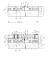
図9(a)は、図1のA−A線に沿う縦断面構造について特に可動電極3d、固定電極4bの構造の配設関係を模式的に示しており、図9(b)は図1のB−B線に沿う縦断面構造について特にアンカ部3c付近の構造について模式的に示している。
FIG. 9A schematically shows the arrangement relationship of the
これらの図9に示すように、センサチップ1は、例えば、p型の単結晶シリコンからなる支持基板9上に絶縁膜としての酸化膜10を介してp型の単結晶シリコン層11を形成したSOI(Silicon On Insulator)基板をベースとしておりマイクロマシニング技術によって単結晶シリコン層11および酸化膜10に溝12を形成することで形成されている。尚、センサチップ1を構成するSOI基板は、図1に示すように、平面的には矩形状(正方形状)に形成されている。酸化膜10は、例えば0.5〜5.0μm程度の膜厚に形成されている。寄生容量を低減するには厚い方が望ましい。
As shown in FIG. 9, in the
図9(a)に示す断面においては、例えばp型の単結晶シリコンによる支持基板7の上に中空状態で固定電極4bおよび可動電極3dがそれぞれ形成されている。これらの固定電極4bおよび可動電極3dは、比較的狭い第1幅W1に形成されている。
In the cross section shown in FIG. 9A, the fixed
また、図9(b)に示す断面においては、支持基板9の上面上にp型不純物(ボロン(B))を含有する酸化膜10によって支持部10bが形成されており、当該支持部10bの上面上にp型不純物(ボロン(B))を含有するシリコン層11が形成されており、このシリコン層11の上面上にアルミニウム(Al)による電極パッド6が形成されている。支持部10bは、その側面10aが内下側に湾曲形成されている。このシリコン層11は、第1幅W1に比較して広い第2幅W2に形成されている。
In the cross section shown in FIG. 9B, a
次に、上記構造の製造方法について説明する。尚、本実施形態の特徴に関わる工程説明を中心に説明を行い、その他の図示しない領域における構造の製造方法説明については省略する。 Next, the manufacturing method of the said structure is demonstrated. The description will focus on the process related to the features of the present embodiment, and the description of the method for manufacturing the structure in other regions not shown will be omitted.
図6ないし図8は、製造途中段階における図9に対応した縦断面構造図を表わしている。まず、図6に示すように、p型単結晶シリコンによる支持基板9の上面上に酸化膜10を介して同一導電型のp型シリコン層11を貼り合わせ法によって形成する。これによりSOI基板を形成できる。このとき、p型不純物(例えばボロン)を含有した酸化膜10が支持基板9の上面上に形成されるが、n型不純物(例えばリン)を含有した酸化膜に比較して不純物濃度が高くなる。
6 to 8 show longitudinal sectional structural views corresponding to FIG. 9 in the middle of manufacturing. First, as shown in FIG. 6, a p-
次に、図7に示すように、アルミニウム(Al)を蒸着、スパッタ法などの方法を用いて形成し、その上に酸化膜、レジスト(図示せず)などのマスクパターンを形成した後、ウェットエッチング処理しアルミニウムを電極パッド6の形状にパターニングする。これにより、SOI基板の上面を荒らすことなくアルミニウムによる電極パッド6を形成でき、性能のばらつきを抑えることができる。
Next, as shown in FIG. 7, aluminum (Al) is formed using a method such as vapor deposition or sputtering, and a mask pattern such as an oxide film or resist (not shown) is formed thereon, and then wet. Etching is performed to pattern aluminum into the shape of the
次に、図8に示すように、p型シリコン層11を異方性エッチング処理し酸化膜10の上面上に達する溝12を形成する。次に、図9に示すように、例えば触媒にメタノールを用いるフッ酸ガスを用いたドライエッチング法によって酸化膜10を等方的にエッチング処理することで支持部10bを残留させながら支持部10b脇の酸化膜10を除去する。
Next, as shown in FIG. 8, the p-
このとき、図9に示した領域においては、可動電極3d、固定電極4b下に位置する酸化膜10が除去されると同時に、アンカ部3cを構成するシリコン層11の中央部下に位置する酸化膜10の側面10aが内下側に湾曲形成され、シリコン層11の直下中央部の酸化膜10のみ支持部10bとして残留する。尚、図9には図示していないが、図1に示す基部4aの形成領域において、酸化膜10は除去処理されていないため、固定部4は支持基板9に安定的に固定される。このようにして、固定電極4b、可動電極3d、アンカ部3cを同時に形成できる。
At this time, in the region shown in FIG. 9, the
図2は、この構造の赤外線吸収率特性、アンカ部におけるp型シリコン層と電極パッドとの間のコンタクト抵抗値についてp型シリコン層の抵抗率との関係について概略的に示している。ダイシング時に赤外光をあてることでアライメントずれの確認を容易にするためには、赤外光の吸収率が低いほうが良い。したがって、赤外光の吸収率を低くするため抵抗率を上げると良く、p型シリコン層11の含有不純物濃度を低くすると良い。逆に、p型シリコン層11と電極パッド6との間のコンタクト抵抗を低くするためにはp型シリコン層11の抵抗率を低くすると良く、この場合、p型シリコン層11の含有不純物濃度を高くすると良い。
FIG. 2 schematically shows the relationship between the infrared absorptivity characteristics of this structure, the contact resistance value between the p-type silicon layer and the electrode pad in the anchor portion, and the resistivity of the p-type silicon layer. In order to facilitate confirmation of misalignment by applying infrared light at the time of dicing, the infrared light absorption rate should be low. Therefore, the resistivity should be increased in order to reduce the infrared light absorption, and the concentration of impurities contained in the p-
これらのトレードオフの関係で調整することが良いが、ダイシング時のアライメントずれを容易に確認するためには吸収率を50%程度以下に抑えると良いため、赤外光の吸収率がこの特性を満たすためには10−2[Ω・cm]以上にすることが好ましい。逆に、コンタクト抵抗を低くするためには抵抗率を10−1[Ω・cm]以下にすることが望ましい。両者を満たすためには、シリコン層11の抵抗率を10−2[Ω・cm]以上10−1[Ω・cm]以下の範囲Tにすると良い。尚、図2に示すコンタクト抵抗値の範囲は、数Ω〜数十Ω程度であり、アルミニウムによる電極パッド6の抵抗、シリコン層11の配線抵抗、などに比較して無視できる程度に低いため適宜調整すると良い。
It is good to adjust in relation to these trade-offs, but in order to easily confirm the misalignment at the time of dicing, it is better to suppress the absorptance to about 50% or less. In order to satisfy this, it is preferable to set it to 10 −2 [Ω · cm] or more. Conversely, in order to reduce the contact resistance, it is desirable to set the resistivity to 10 −1 [Ω · cm] or less. In order to satisfy both, it is preferable to set the resistivity of the
図3および図4は、従来から用いられているn型シリコン基板を適用した場合とp型シリコン層を適用した場合の歪み状態の比較を模式的に示している。
これらの図3および図4に示すように、リン(P)などのn型不純物がドープされたシリコン基板13をデバイスウェハとし、酸化膜10を介して貼り合わせ法により貼り合わせて作成した場合には、発明者らの検討結果によれば酸化膜10が楔となってしまい、n型シリコン基板13との界面(シリコン基板13の下面)と酸化膜10の側面との間の角度が鋭角になりやすく、図4に示すように歪が大きくなりやすいことが判明している。本実施形態では、p型シリコン基板11をデバイスウェハとして貼り合わせて形成しているため、歪みを極力小さく抑えることができる。
3 and 4 schematically show a comparison of strain states when a conventional n-type silicon substrate is applied and when a p-type silicon layer is applied.
As shown in FIG. 3 and FIG. 4, when a
図5は、p型不純物を含有したシリコン層を適用した場合とn型不純物を含有したシリコン層を適用した場合における各シリコン層11、13の歪み状態の温度特性を示している。この図5に示すように、環境温度を上昇させると、これに伴い歪み率も上昇するが、n型不純物を適用した場合には温度による歪み率の変動が大きく、p型不純物を適用した場合には変動が小さい。したがって、特に車両用途に適用する場合には過酷な環境下にて使用されるため、p型不純物を含有したシリコン層11を適用することが望ましいことがわかる。
FIG. 5 shows the temperature characteristics of the strain states of the silicon layers 11 and 13 when a silicon layer containing p-type impurities is applied and when a silicon layer containing n-type impurities is applied. As shown in FIG. 5, when the environmental temperature is raised, the strain rate is also increased. However, when n-type impurities are applied, the variation of the strain rate due to temperature is large, and when p-type impurities are applied. The fluctuation is small. Therefore, it is understood that it is desirable to apply the
本実施形態によれば、互いに離間した可動電極3d、固定電極4bを具備し、電極3d、4d間の静電容量の変化を力学量として検出する加速度センサAの製造方法において、支持基板9の上面上にp型不純物がドープされた酸化膜10を介して形成されたシリコン層11について当該シリコン層11を第1幅W1の第1電極部分となる可動電極3d、固定電極4bと、第1幅W1よりも広い第2幅W2の第2電極部分となるp型シリコン層11(可動部3の一部)とを酸化膜10の上面が露出するまで例えば異方性エッチング処理によって分断処理することで複数に加工し、露出した酸化膜10をp型シリコン層11の下の中央寄りの支持部10bを残留させながら支持部10b脇の酸化膜10を例えば等方性エッチングにより除去しているため、p型シリコン層11および酸化膜10との間の界面の間のエッチングレートが遅くなることで接合面に楔が入りにくくなり応力集中を緩和でき機械的信頼性を向上できる。
According to the present embodiment, in the method of manufacturing the acceleration sensor A that includes the
また、シリコン層11の上面上にアルミニウムによる電極パッド6を形成するときにはウェットエッチング処理によって形成しているため、シリコン層11の特性を劣化することなく形成できるようになる。
Further, since the
また、シリコン層11には不純物が高濃度にドープされているため、p型シリコン層とアルミ電極パッドとの接合にオーミックコンタクトを適用でき、シリコン層11に改めてインプランテーション技術によって不純物を導入するプロセスを必要とすることなく構成できる。
Further, since the
酸化膜10が、支持基板9上に当該支持基板9上から上側に幅が狭くなるように形成されp型不純物がドープされており側面10aが下側に凹湾曲形成されており、p型不純物がドープされたシリコン層11が当該酸化膜10上に形成されているため、応力集中を緩和することができ機械的信頼性を向上できる。また、温度変化に伴う歪み率の安定性を向上できる。
The
シリコン層11の抵抗率範囲を0.01〜0.1[Ω・cm]として設定しているため、コンタクト抵抗を十分に低く構成しながら、赤外線吸収率を十分に低く保って形成することができる。したがって、赤外線の十分な透過率を確保することができ赤外線を用いてダイシング時のアライメントを容易に観察できるようになり、アライメントずれを防ぐことができる。
Since the resistivity range of the
(第2の実施形態)
図10ないし図15は、本発明の第2の実施形態を示すもので、前述実施形態と異なるところは、キャップ基板とセンサ基板とを設けた形態に適用しているところにある。また、キャップ基板に貫通電極を形成してセンサ基板に形成された半導体層との接続を図っているところにある。
(Second Embodiment)
10 to 15 show a second embodiment of the present invention. The difference from the above-described embodiment is that it is applied to a configuration in which a cap substrate and a sensor substrate are provided. In addition, a through electrode is formed on the cap substrate to connect with a semiconductor layer formed on the sensor substrate.
なお、本実施形態以降の実施形態では、前述実施形態のセンサ構造に当該センサ構造を覆ってキャビティを形成したキャップ基板を組み合わせた構造およびその製造工程に特徴を備えている。 Note that the embodiments after this embodiment are characterized by a structure in which the sensor structure of the above-described embodiment is combined with a cap substrate that covers the sensor structure and has a cavity, and the manufacturing process thereof.
図10は、キャップ基板とセンサ基板の要部の縦断面構造を概略的に示している。
図11(a)は、図10のC−C線に沿って示すセンサ基板およびその周辺の平面構造を示し、図11(b)は、図10のD−D線に沿って示すキャップ基板およびその周辺の平面構造を示している。また、図12(c)は、図10のE−E線に沿ってキャップ基板の表面状態を示している。なお図10は、図11(b)のF−F線に沿う縦断面構造を示している。図11(a)に示すように、センサ基板21の平面構造は図1に示すセンサチップ1の平面構造とほぼ同一であるため、同一機能を有する部分に同一符号を付して説明を省略する。
FIG. 10 schematically shows a longitudinal sectional structure of the main part of the cap substrate and the sensor substrate.
FIG. 11A shows the sensor substrate shown along the line CC in FIG. 10 and the planar structure around it, and FIG. 11B shows the cap substrate shown along the line DD in FIG. The surrounding planar structure is shown. FIG. 12C shows the surface state of the cap substrate along the line EE in FIG. FIG. 10 shows a longitudinal sectional structure taken along line FF in FIG. As shown in FIG. 11A, the planar structure of the
図10に示すように、センサ基板21上に接触するようにキャップ基板22が設けられている。キャップ基板22は、p型シリコン基板による支持基板(第2支持基板に相当)22aを母体として構成されている。支持基板22aには凹部22aaが裏面(下面)側に形成されており、キャップ基板22は、支持基板22aの凹部22aaを含み上下外周面を覆うように絶縁膜22bが形成されることによって構成される。凹部22aaは可動電極3d、固定電極4bなどの電気的構成要素が可動自在にする空間(キャビティ)を形成するために設けられている。
As shown in FIG. 10, a
キャップ基板22には、シリコン層11の上面と接続する電極24〜26が当該キャップ基板22内を貫通する貫通電極として設けられている。各電極24〜26は、支持基板22aに形成されたホール(符号なし)内に絶縁膜22b、23を介して形成されており、支持基板22aとの間では構造的に非接触状態に形成されている。
In the
電極24は、アンカ部3cと構造的および電気的に接続するように構成されている。電極25は、周辺部27のシリコン層11の上面と構造的に接触するように構成されている。図11(a)に示すように、周辺部27は、電位を一定の定電位(例えばグランド電位)に固定するため、各電極3d、4bの周辺に位置して当該電極3d、4bから離間して平面的にその周囲を覆うように設けられている。図10に示すように、電極28が、キャップ基板22の絶縁膜22bを貫通して支持基板22aと構造的に接続するように設けられている。
The
図11(b)および図12(c)に示すように、電極26は固定部4の基部4aと接続するように構成されている(接触部分の縦断面構造は図示せず)。電極24〜26、28は、それぞれ、アルミニウム(Al)、銅(Cu)などのメタル、もしくは、高濃度のp型不純物が添加されたシリコンにより構成されている。
As shown in FIGS. 11B and 12C, the
例えば、電極24〜26、28が、アルミニウム(Al)、銅(Cu)により形成されている場合には、高濃度に不純物がドープされたp型シリコン層11と当該金属電極との間のオーミックコンタクトを適用することができる。したがって、シリコン層11に拡散層を形成するプロセスを必要とすることなく構成でき、前述実施形態とほぼ同様の作用効果を奏する。
For example, when the
上記構造の製造方法について図13〜図14を用いて説明する。
図13(a)に示すように、平板状のシリコン基板上にホトリソグラフィ技術を用いてレジスト(図示せず)をパターン形成し、シリコン基板をエッチング処理することで凹部22aaを形成し、処理後の支持基板22aに対して全面酸化処理を施すことで絶縁膜22bを形成する。
The manufacturing method of the said structure is demonstrated using FIGS. 13-14.
As shown in FIG. 13 (a), a resist (not shown) is patterned on a flat silicon substrate using a photolithographic technique, and the recess 22aa is formed by etching the silicon substrate. An insulating
図13(b)に示すように、センサ基板21は、p型の単結晶シリコンからなる支持基板9に酸化膜10を介してp型の単結晶シリコン層11を貼り合わせて形成したSOI基板をベース(基部)として形成する。尚、センサ基板21としてはSOI基板に代えて、支持基板9上に酸化膜10を形成した後、当該酸化膜10の上面上にCVD法を用いて高濃度のp型不純物が添加されたポリシリコンを堆積してシリコン層11を形成するようにしても良い。
As shown in FIG. 13B, the
図13(c)に示すように、シリコン層11の上にホトリソグラフィ技術を用いてレジスト(図示せず)をパターン形成し、前述実施形態と同様の条件下でアンカ部3c下の酸化膜10の支持部10bを残留させながら可動電極3d、固定電極4b下の酸化膜10を全て除去処理する。
As shown in FIG. 13C, a resist (not shown) is patterned on the
洗浄処理を行ってから、図13(d)に示すように、センサ基板21とキャップ基板22を接合する。この接合処理には、例えばフュージョン処理、プラズマ活性処理、常温接合処理が用いられる。
After performing the cleaning process, the
図14(e)に示すように、キャップ基板22上にホトリソグラフィを用いてレジスト(図示せず)をパターン形成し、アンカ部3c、周辺部27の上面上に至るまでエッチング処理を施して貫通孔を形成する。尚、同時または別工程で固定部4の基部4a上に至る貫通孔を形成するが、図示していない。
As shown in FIG. 14E, a resist (not shown) is patterned on the
図14(f)に示すように、キャップ基板22のホール内に例えば熱酸化処理、CVD法、スパッタ法などの何れかの方法で酸化膜23を形成する。次に、ホトリソグラフィにより酸化膜23の上面上にレジスト(図示せず)をパターン形成し、酸化膜22b、23をエッチングすることでシリコン層11の上面上に至るまで貫通孔を形成する。尚、図14(f)では、酸化膜23を熱酸化処理により内面に形成した後、シリコン層11の上面上の酸化膜23を除去した後の状態を示している。
As shown in FIG. 14F, an
次に、図10に示すように、アルミニウム(Al)、銅(Cu)、または、p型不純物が高濃度にドープされたシリコンにより電極24〜26、28(電極26は図11参照)をシリコン層11の上に接触するように形成する。すると、アンカ部3cに接続するためのコンタクトと、キャップ基板22を構成する支持基板22aの電位を取得するためのコンタクトとを形成できる。
Next, as shown in FIG. 10, the
この後、図15に示すように、ホトリソグラフィによりレジスト(図示せず)をパターニングし、埋め込まれた電極24〜26、28の中央部分をエッチングして除去するようにしても良い。すると、工程上の熱処理の影響を受けて電極24〜26、28が膨張し他の構造に影響を及ぼすことでデバイスの信頼性を損ねる不具合を防ぐことができる。尚、この除去処理工程は必要に応じて設ければ良い。
Thereafter, as shown in FIG. 15, a resist (not shown) may be patterned by photolithography, and the central portions of the embedded
本実施形態によれば、p型の支持基板9上にp型不純物がドープされた酸化膜10bを介してp型不純物がドープされたシリコン層11が形成されており、当該シリコン層11の上面上にキャップ基板22内に構成される電極24をp型不純物がドープされたシリコンにより形成したので、拡散層レスで形成することができ、抵抗率範囲を広くして特性を良化して構成することができる。拡散層を形成する必要がないため、工程を簡素化することができる。
According to the present embodiment, the
また、キャップ基板22とセンサ基板21とを分離して形成し、キャップ基板22を貫通する電極24〜26を形成してセンサ基板21に形成されたシリコン層11との間の接続を図っているため、前述実施形態とほぼ同様の作用効果を奏する。
In addition, the
(第3の実施形態)
図16および図17は、本発明の第3の実施形態を示すもので、前述実施形態と異なるところは、キャップ基板を構成する母体となる支持基板の構成を貫通電極の主構造としているところにある。また、エアアイソレーションを適用してキャップ基板を構成する他の構造との間で絶縁を図っているところにある。前述実施形態と同一機能を有する部分には同一符号を付して説明を省略し、前述実施形態と異なる部分を中心に説明する。
(Third embodiment)
FIGS. 16 and 17 show a third embodiment of the present invention. The difference from the above-described embodiment is that the structure of the support substrate serving as a base constituting the cap substrate is the main structure of the through electrode. is there. In addition, air isolation is used to insulate from other structures constituting the cap substrate. Portions having the same functions as those in the previous embodiment are denoted by the same reference numerals, description thereof is omitted, and portions different from those in the previous embodiment will be mainly described.
図16(a)は、図11(a)に対応した平面図を示しており、図16(b)は、図11(b)に対応した平面図を示している。また、図17(e)は、図16(a)のG−G線に沿う縦断面図を示している。 FIG. 16A shows a plan view corresponding to FIG. 11A, and FIG. 16B shows a plan view corresponding to FIG. 11B. Moreover, FIG.17 (e) has shown the longitudinal cross-sectional view which follows the GG line of Fig.16 (a).
図16(a)、図16(b)、図17(e)に示すように、キャップ基板22に代わるキャップ基板32が設けられている。図17(e)に示すように、このキャップ基板32は、前述実施形態の支持基板22aおよび絶縁膜22bと共に、支持基板22aを加工して形成されたシリコン層22cを備えている。シリコン層22cは、電解めっき部22dを介してアンカ部3cに対して電気的に接続する貫通電極として構成されている。シリコン層22c、電解めっき部22dは、隣り合う支持基板22aとの間に空間が設けられており、これによりエアアイソレーションによる絶縁状態が保持されている。
As shown in FIGS. 16A, 16B, and 17E, a
上記構造の製造方法を説明する。
図17(a)に示すように、キャップ基板32を構成する支持基板22aの露出全面に絶縁膜22bを形成する。図17(b)に示すように、コンタクト部分となる領域にホトリソグラフィによりレジスト(図示せず)をパターニングし、絶縁膜22bの下面(裏面)をエッチング処理し開口22eを形成する。図17(c)に示すように、支持基板22aの表面に形成された酸化膜22bをRIEなどのドライエッチング処理、CMP法、フッ酸を用いたウェットエッチングなどを用いて除去処理し、さらに、シリコン基板2の下面(裏面)が露出した開口22eに電解めっき処理を施すことで電解めっき部22dを形成し、支持基板22aとの間で電気的導通を図る。
The manufacturing method of the said structure is demonstrated.
As shown in FIG. 17A, an insulating
図17(d)に示すように、センサ基板21のアンカ部3cを構成するシリコン層11の上面と電解めっき部22dとを接合すると共に、周辺部27を構成するシリコン層11の上面と電解めっき部22dとを接合するように、キャップ基板32とセンサ基板21とを接合する。
As shown in FIG. 17 (d), the upper surface of the
図17(e)に示すように、RIE法などの異方性エッチング処理によりアンカ部3cを構成するシリコン層11の上面、周辺部27の上面に達するトレンチ溝(貫通孔)22fを支持基板22aに形成することで、シリコン層22cを他の支持基板22aの形成部分と分離するように形成することでエアアイソレーション構造を得る。この場合、絶縁膜22bの上面上に達するようにトレンチ溝22fを形成した後、別工程で絶縁膜22bを除去処理しても良い。
As shown in FIG. 17E, trench grooves (through holes) 22f reaching the upper surface of the
本実施形態によれば、支持基板22aをエッチング処理してシリコン層22cを他の支持基板22aの形成部分と分離するように形成しているため、エアアイソレーション構造を適用することができ、寄生容量を低減できる。また、前述実施形態とほぼ同様の電気的接続構造を得ることができ、同様の作用効果が得られる。
According to the present embodiment, since the
(第3の実施形態の変形例)
図18および図19は、本発明の第3の実施形態の変形例を示すもので、第3の実施形態と異なるところは、貫通孔(トレンチ溝)の形成領域を変更し、支持基板の凹部に形成された絶縁膜に達するまで貫通孔を形成しているところにある。
(Modification of the third embodiment)
18 and 19 show a modification of the third embodiment of the present invention. The difference from the third embodiment is that the formation region of the through hole (trench groove) is changed, and the concave portion of the support substrate is changed. The through hole is formed until reaching the insulating film formed in (1).
図18(a)に示すように、絶縁膜22bは支持基板22aの凹部22aaに沿って形成されているが、トレンチ溝22fは支持基板22aの凹部22aa形成領域に形成された絶縁膜22bの上面上に至るまで形成されている。これにより、エアアイソレーション構造が形成されている。この構造によれば、支持基板22aの上面のコンタクト部の面積を大きくすることができるため、例えば、当該露出面上にワイヤボンディングしたり、バンプで接続する場合などでも容易に形成できる。
As shown in FIG. 18A, the insulating
この場合、RIE法などの異方性エッチング処理を用いてトレンチ溝22fを形成するが、絶縁膜22bとの間で選択比を有する条件を適用してエッチング処理を行うことで、エッチング時間調整を厳密に調整しなくても絶縁膜22bの上面上でエッチング処理を終了させることができる。したがって、トレンチ溝22fが空間(キャビティ)に至ることを防止することができ、空間の気密性を保持することができる。トレンチ溝22fを凹部22aaの形成領域に形成するため、エッチング時間を短くすることができる。
In this case, the
シリコン層22c、電解めっき部22dによるコンタクト部は、エアアイソレーション構造を採用しているため、周囲の他領域の支持基板22aとの間で絶縁状態を保ちながらシリコン層11の上面と接触状態に形成できる。
Since the contact portion formed by the
図19は、他の変形例について縦断面構造を概略的に示している。この図19(a)および図19(b)に示すように、絶縁膜22bが支持基板22aの凹部22aaに沿って形成されており、その絶縁膜22bは凹部22aaが上下(縦)方向に延伸する部分にも沿って形成されている。この絶縁膜22bの上下(縦)方向に延伸する部分に縦延伸部22bbとして図19(a)および図19(b)中に符号を付している。
FIG. 19 schematically shows a longitudinal sectional structure of another modification. As shown in FIGS. 19A and 19B, the insulating
これらの図19(a)および図19(b)に示すように、トレンチ溝22fは、平面的に縦延伸部22bbが形成された平面領域に合わせて形成されている。トレンチ溝22fを例えばRIE法などの異方性エッチング処理を用いて形成する際、絶縁膜22bに対して選択性を有する条件にて支持基板22aをエッチング処理すると、縦延伸部22bbが上下(縦)方向に延伸しているため、たとえオーバーエッチング気味にエッチング時間を調整したとしても絶縁膜22bの縦延伸部22bbにおいてエッチング処理が確実に停止する。したがって、前述実施形態に比較して、トレンチ溝22fが空間(キャビティ)に至ることをさらに防止することができ、空間の気密信頼性を向上することができる。
As shown in FIGS. 19A and 19B, the
(第4の実施形態)
図20は、本発明の第4の実施形態を示すもので、前述実施形態と異なるところは、コンタクト部分について電解めっき処理に代えてシリコン層を形成した後、エアアイソレーション構造を形成しているところにある。前述実施形態と同一部分については同一符号を付して説明を省略する。
(Fourth embodiment)
FIG. 20 shows a fourth embodiment of the present invention. The difference from the previous embodiment is that an air isolation structure is formed after a silicon layer is formed on the contact portion instead of electrolytic plating. By the way. The same parts as those in the previous embodiment are denoted by the same reference numerals and the description thereof is omitted.
図20(d)は、図16(a)のG−G線に沿う縦断面構造図を示している。
図20(d)に示すように、キャップ基板22に代わるキャップ基板42は、前述実施形態にて説明した支持基板22a、絶縁膜22b、シリコン層22cと共に、p型シリコン層22gを備えている。このp型のシリコン層22gは前述実施形態の電解めっき部22dに代えて設けられている。したがって、シリコン層22gはシリコン層22cとアンカ部3cとの間に介在して形成されている。
FIG. 20D shows a longitudinal sectional structural view along the line GG in FIG.
As shown in FIG. 20D, a
上記構造の製造方法について説明する。図17(b)に示す構造を形成した後、図20(a)に示すように、p型のシリコン層22gについて開口22eの形成領域を含んでキャップ基板42の下面(裏面)側に沿って形成する。支持基板22aには凹部22aaが形成されているが、シリコン層22gはこの凹部22aaに沿って形成されている。シリコン層22gは、シリコン層11との間に空間が設けられ当該シリコン層11と非接触状態で構成されている。尚、p型のシリコン層22gの形成方法は、エピタキシャル成長でも良いし、CVD法によりp型不純物が高濃度にドープされたポリシリコンを堆積するようにしても良い。
The manufacturing method of the said structure is demonstrated. After the structure shown in FIG. 17B is formed, as shown in FIG. 20A, the p-
図20(b)に示すように、キャップ基板42の上面(表面)側に形成された絶縁膜22bを除去処理する。この除去処理方法は、支持基板22aの下面(裏面)側をレジストなどで保護しフッ酸(HF)などを用いたエッチャントによって支持基板22aの上面(表面)側を処理する方法、RIE法などのドライエッチング処理を用いる方法、CMP処理によって平坦化処理する方法などが適用できる。その後、キャップ基板42の下面(裏面)側について絶縁膜22bをストッパーとしてCMP法により平坦化処理する。
As shown in FIG. 20B, the insulating
図20(c)に示すように、キャップ基板42とセンサ基板21とを接合する。このとき、シリコン層22gがシリコン層11と接触して形成されるようになる。したがって、前述実施形態と同様に、拡散層を形成することなく構成できる。これにより、前述実施形態とほぼ同様の電気的接続構造を得ることができ、同様の作用効果が得られる。
As shown in FIG. 20C, the
(第4の実施形態の変形例)
図21は、本発明の第4の実施形態の変形例を示すもので、第4の実施形態と異なるところは、キャップ基板の支持基板に貫通孔を形成する前に、支持基板の下面に絶縁膜と当該絶縁膜とは異なる材質の材質膜との2層構造で構成したところにある。
(Modification of the fourth embodiment)
FIG. 21 shows a modification of the fourth embodiment of the present invention. The difference from the fourth embodiment is that the insulation is formed on the lower surface of the support substrate before the through hole is formed in the support substrate of the cap substrate. The film and the insulating film are in a two-layer structure of a material film made of a different material.
図21(a)に示すように、トレンチ溝(貫通孔)22fは、凹部22aaの形成領域に形成されており、当該トレンチ溝22fの平面的な形成領域において絶縁膜22bが支持基板22aの凹部22aaに沿って形成されており、さらにシリコン層22gが絶縁膜22bの下面を覆うように絶縁膜22bの材質とは異なる膜により形成されている。この場合、シリコン層22gはストッパー膜として機能し、気密信頼性を向上するための膜として設けられている。
As shown in FIG. 21A, the trench groove (through hole) 22f is formed in the formation region of the recess 22aa, and the insulating
要するに、トレンチ溝22fを形成するときには、支持基板22aをRIE法により異方性エッチング処理し絶縁膜22bの上面上にてエッチングをストップすることが望ましいが、万が一突き抜けてしまう虞がある。この場合、絶縁膜22bの下面を覆うようにシリコン層22gが設けられているため、当該シリコン層22gと絶縁膜22bとの間で選択比を取得できる条件にてエッチング処理を施すことで、少なくともシリコン層22gの上面上にてエッチング処理をストップさせることができ、キャップ基板42とセンサ基板21との間に構成される空間(キャビティ)の気密信頼性を向上でき、強度が高くなる。
In short, when the
(第5の実施形態)
図22は、本発明の第5の実施形態を示すもので、前述実施形態と異なるところは、コンタクト部分に電解めっき処理を施した後、金属を貫通電極上に形成し、エアアイソレーションを形成しているところにある。前述実施形態と同一部分については同一符号を付して説明を省略する。
(Fifth embodiment)
FIG. 22 shows a fifth embodiment of the present invention. The difference from the previous embodiment is that after the electrolytic plating process is performed on the contact portion, a metal is formed on the through electrode to form an air isolation. It is in place. The same parts as those in the previous embodiment are denoted by the same reference numerals and the description thereof is omitted.
図22(d)に示すように、キャップ基板32に代わるキャップ基板52は、前述実施形態にて説明した支持基板22a、絶縁膜22b、シリコン層22c、電解めっき部22dと共に、シリコン層22cの上面上に形成されたアルミニウム(Al)などの金属電極22hを備えている。
As shown in FIG. 22D, a
上記構造の製造方法について説明する。図17(c)に図示した構造と同一構造に至るまで前述のプロセスを適用してキャップ基板52を形成する。すると図22(a)に示すように、支持基板22aの下面の露出部に電解めっき部22dが形成される。図22(b)に示すように、電解めっき部22dの直上方に位置して金属電極22hを突起状に形成する。図22(c)に示すように、センサ基板21とキャップ基板52とを接合し、図22(d)に示すように、トレンチ溝22fを形成する。
The manufacturing method of the said structure is demonstrated. The
本実施形態によれば、コンタクト部分に電解めっき部22dを形成した後、金属電極22hを貫通電極となるシリコン層22cの上面上に形成し、その後、トレンチ溝22fを形成することでエアアイソレーション構造を形成しているため、前述実施形態とほぼ同様の電気的接続構造を得ることができ、同様の作用効果が得られる。支持基板22a上に突起状の電極22hが形成されるため、フリップチップ実装しやすくなる。
According to the present embodiment, after the
(第6の実施形態)
図23ないし図25は、本発明の第6の実施形態を示すもので、前述実施形態と異なるところは、センサ基板が可動電極の両側に離間して固定電極を備えているところにある。前述実施形態と同一部分には同一符号を付して説明を省略し、以下、異なる部分について説明する。
(Sixth embodiment)
FIGS. 23 to 25 show a sixth embodiment of the present invention. The difference from the above-described embodiment is that the sensor substrate is provided with fixed electrodes spaced apart on both sides of the movable electrode. The same parts as those of the above-described embodiment are denoted by the same reference numerals, description thereof is omitted, and different parts will be described below.
図23(a)は、固定電極および可動電極の配設構造を概略的に表す平面図を示しており、図23(b)は、電極の配設構造を概略的に表す平面図を示している。また、図25(e)は、図23(a)のH1−H1線およびH2−H2線に沿って示す縦断面構造を概略的に表している。 FIG. 23A is a plan view schematically showing the arrangement structure of the fixed electrode and the movable electrode, and FIG. 23B is a plan view schematically showing the arrangement structure of the electrodes. Yes. FIG. 25E schematically shows a vertical cross-sectional structure shown along the lines H1-H1 and H2-H2 in FIG.
図23(a)に示すように、電極29は電極24が接触する固定部4の基部4aとは別の固定部4の基部4aに接触するように設けられている。固定電極4bはこの基部4aから構造的に延びて構成されており、複数の隣り合う可動電極3dおよび3d間の中央に位置するように配設されている。すなわち、電極29が接触する基部4aの島は、電極24が接触する基部4aの島とは別の領域に設けられている。
As shown in FIG. 23A, the
図25(e)に示すように、センサ基板21に代わるセンサ基板31は、前述実施形態にて説明した支持基板9、酸化膜10、シリコン層11を備えると共に、シリコン層11の上層に形成される酸化膜10cと、シリコン層11の上に酸化膜10cを介して接続されるシリコン層11aとを備えている。尚、酸化膜10cは犠牲層として設けられる。
As shown in FIG. 25 (e), a
支持基板9上には、酸化膜10、シリコン層11、酸化膜10cの主部、シリコン層11aの主部、が順に積層された積層構造により構成されている。シリコン層11aの主部は、酸化膜10cに形成された孔を通じてシリコン層11と接触して構成されている。
On the
シリコン層11の同層の層構造のうち、電極29に電気的に接続されたシリコン層11bは、シリコン層11aの下層側を跨いでシリコン層11a−11a間を電気的に接続して構成されている。したがって、可動電極3d−3d間の中央に位置して固定電極4bを構成することができる。シリコン層11bは、p型不純物が高濃度にドープされたポリシリコンにより形成されている。
Of the same layer structure of the
上記構造のうちセンサ基板31の製造方法について図24および図25を参照しながら説明する。図24(a)に示すように、支持基板9の上に酸化膜10を形成し、酸化膜10の上にp型のシリコン層11を形成する。このシリコン層11の形成方法は、p型の単結晶シリコン基板を貼り合わせ法により貼り合わせても良いし、p型不純物が高濃度にドープされたポリシリコンをCVD法により堆積することによって形成しても良い。
A method for manufacturing the
図24(b)に示すように、シリコン層11の上にホトリソグラフィによりレジスト(図示せず)をパターン形成し、シリコン層11をエッチング処理することで酸化膜10の上面上に至るまでエッチング処理し、シリコン層11の上面および側面を覆うように酸化膜10cを形成する。
As shown in FIG. 24B, a resist (not shown) is patterned on the
図24(c)に示すように、酸化膜10c上にホトリソグラフィによりレジスト(図示せず)をパターン形成してシリコン層11の上面に至るまでエッチング処理することで開口を形成し、当該開口を埋込むと共に酸化膜10cの上面上にシリコン層11aを堆積する。
As shown in FIG. 24C, a resist (not shown) is formed by patterning on the
図25(d)に示すように、シリコン層11a上にホトリソグラフィによりパターン形成し、シリコン層11aにトレンチを形成することでシリコン層11aを複数に分断加工する。この後、露出した酸化膜10cと共に酸化膜10を等方性エッチング処理することで、図25(d)の断面で示す固定電極4b、可動電極3d下の酸化膜10c、10を全て除去処理すると共に、電極24、29の形成領域(図25(e)参照)下方の中央寄りの支持部10bを残留させながら当該支持部10b脇の酸化膜10を除去処理する。またこれと同時に、周辺部27の下の中央寄りの支持部10bを残留させながら当該支持部10b脇の酸化膜10を除去処理する。
As shown in FIG. 25D, a pattern is formed on the
図25(e)に示すように、キャップ基板22とセンサ基板31とを接合処理し、その後、キャップ基板22を貫通するように電極24〜26、28〜29を形成する。
本実施形態によれば、センサ基板31が可動電極3dの両側に離間して固定電極4bを備えているため、前述実施形態に比較して固定電極4bおよび可動電極3d間の容量変化を大きく得ることができる。また、前述実施形態とほぼ同様の電気的接続構造を得ることができ、同様の作用効果が得られる。
As shown in FIG. 25 (e), the
According to the present embodiment, since the
(第7の実施形態)
図26は、本発明の第7の実施形態を示すもので、第6の実施形態と異なるところは、キャップ基板を構成するシリコン層を貫通電極として形成しているところにある。また、エアアイソレーションを適用して他のシリコン層との絶縁を図っているところにある。 図26に示すように、前述の図25(e)に示す構造に対し第4の実施形態で説明したp型のシリコン層22c、p型のシリコン層22gが構成されている。このような実施形態においても前述実施形態とほぼ同様の電気的接続構造を得ることができ、同様の作用効果を奏する。
(Seventh embodiment)
FIG. 26 shows a seventh embodiment of the present invention. The difference from the sixth embodiment is that a silicon layer constituting a cap substrate is formed as a through electrode. In addition, air isolation is used to insulate from other silicon layers. As shown in FIG. 26, the p-
(第8の実施形態)
図27ないし図28は、本発明の第8の実施形態を示すもので、第6の実施形態と異なるところは、センサ基板を構成する支持基板の電位をキャップ基板の上から取得する構造に適用したところにある。前述実施形態と同一部分については同一符号を付して説明を省略する。
(Eighth embodiment)
27 to 28 show an eighth embodiment of the present invention. The difference from the sixth embodiment is that it is applied to a structure in which the potential of the support substrate constituting the sensor substrate is obtained from above the cap substrate. There is. The same parts as those in the previous embodiment are denoted by the same reference numerals and the description thereof is omitted.
図28(e)に示すように、センサ基板31に代わりセンサ基板41が構成されている。このセンサ基板41がセンサ基板31と異なるところは、支持基板9とシリコン層11とを接続するようにシリコン層11cを形成しているところである。さらに、キャップ基板22に代わるキャップ基板72には、電極24〜26、28〜29が設けられていると共に、電極30が、センサ基板41を構成するシリコン層11cと一体のシリコン層11上に接触したシリコン層11aの上面上に形成されているところである。すると、キャップ基板72上に突出した電極30から支持基板9の電位を取得できるようになる。
As shown in FIG. 28 (e), a
上記構造の製造方法について説明する。図27(a)に示すように、支持基板9の上に酸化膜10を形成した後、図27(b)に示すように、酸化膜10上にホトリソグラフィによりレジスト(図示せず)をパターン形成し、酸化膜10に支持基板9の上面上に至る開口を形成し、当該開口にシリコン層11cを埋込むと同時に酸化膜10の上にシリコン層11を形成する。シリコン層11の上にホトリソグラフィによりレジスト(図示せず)をパターン形成し、エッチング処理することで酸化膜10の上面上に至る開口を形成し、当該開口内に酸化膜10cを形成すると共にシリコン層11の上に酸化膜10cを形成する。
The manufacturing method of the said structure is demonstrated. As shown in FIG. 27A, after an
図27(c)に示すように、酸化膜10cに開口を形成し、シリコン層11aを開口内および酸化膜10c上に堆積することで当該シリコン層11aをシリコン層11に接触させ、シリコン層11aをCMP法により平坦化する。
As shown in FIG. 27C, an opening is formed in the
図28(d)に示すように、シリコン層11a上にホトリソグラフィによりレジスト(図示せず)をパターン形成し、シリコン層11aにトレンチを形成することでシリコン層11aを複数に分断加工する。この後、露出した酸化膜10cと共に酸化膜10を等方性エッチング処理することで、図28(d)の断面で示す固定電極4b、可動電極3d下の酸化膜10c、10を全て除去処理すると共に、アンカ部3cの下の中央寄りの支持部10bを残留させながら当該支持部10b脇の酸化膜10を除去処理する。
As shown in FIG. 28 (d), a resist (not shown) is patterned on the
図28(e)に示すように、キャップ基板72とセンサ基板41とを接合し、キャップ基板72を貫通するように電極24〜26、28〜30を形成する。
本実施形態によれば、シリコン層11(11a、11c)、支持基板9が共にp型不純物がドープされたシリコンにより形成されているため、拡散層レスで形成することができ、前述実施形態とほぼ同様の作用効果が得られる。また、シリコン層11cが周辺部27のシリコン層11と支持基板9との間に構造的に接続するように構成されているため、各シリコン層11(11a、11c)と支持基板9との電位を同一電位に保つことができ、可動電極3d(可動部3)と支持基板9との間に発生する寄生容量が低減されるようになる。これにより、可動部3の感度を良化することができる。特に、キャップ基板72内の電極30と、周辺部27のシリコン層11a、11と、支持基板9との間の電位を一定にすることができるため、ノイズを低減できる。
As shown in FIG. 28 (e), the
According to this embodiment, since both the silicon layer 11 (11a, 11c) and the
(第9の実施形態)
図29は、本発明の第9の実施形態を示すもので、第8の実施形態と異なるところは、キャップ基板を構成する支持基板を貫通電極の主構造として形成しているところにある。また、エアアイソレーションを適用し貫通電極をセンサ基板の他の構造と絶縁しているところにある。図29に示すように、前述の図28(e)に示す電極24、25、29、30として、それぞれ第4の実施形態で説明したp型不純物がドープされたシリコン層22c、p型不純物がドープされたシリコン層22gが構成されている。このような実施形態においても前述実施形態とほぼ同様の電気的接続構造を得ることができ、同様の作用効果を奏する。
(Ninth embodiment)
FIG. 29 shows a ninth embodiment of the present invention, which is different from the eighth embodiment in that a support substrate constituting a cap substrate is formed as a main structure of the through electrode. In addition, air isolation is applied to insulate the through electrode from other structures of the sensor substrate. As shown in FIG. 29, as the
(第10の実施形態)
図30および図31は、本発明の第10の実施形態を示すもので、上下方向の容量変化を検出できるようにしているところに特徴を有している。また、センサ基板とキャップ基板との接合部分にセンサ基板側の材質とキャップ基板側の材質と同一材質により別体で形成されているところに特徴を備えている。また、センサ基板との接合面となるキャップ基板の所定面にセンサ基板の接合部と同一材料により膜を予め形成した後、センサ基板とキャップ基板との間を構造的に接触させるようにしているところに特徴を有している。
(Tenth embodiment)
30 and 31 show a tenth embodiment of the present invention, which is characterized in that a change in capacitance in the vertical direction can be detected. Further, the sensor substrate and the cap substrate are characterized in that they are separately formed of the same material as the material on the sensor substrate side and the material on the cap substrate side at the joint portion between the sensor substrate and the cap substrate. In addition, after a film is formed in advance on the predetermined surface of the cap substrate, which is a bonding surface with the sensor substrate, using the same material as the bonding portion of the sensor substrate, the sensor substrate and the cap substrate are structurally brought into contact with each other. However, it has the characteristics.
図31(e)に示すように、キャップ基板22に代わるキャップ基板72は、支持基板22a、絶縁膜22bと共に、センサ基板21との間の接合面となる少なくとも一部の所定面にシリコン層22iが形成されることによって構成されている。
As shown in FIG. 31E, a
このシリコン層22iは、例えばポリシリコンにより形成され、シリコン層11との接合部と同一材料によって構成されている。シリコン層22iは電極24、25とシリコン層11との間に介在して形成されている。本実施形態では、センサ基板21を用いた実施形態を示すが、前述したセンサ基板31、41を適用しても良い。
The
シリコン層22iの横延設部22iaが絶縁膜22bの下側に沿って形成されている。
横延設部22iaは、可動電極3dの上方に位置してキャップ基板72に固定設置されるもので、可動電極3dが上下方向に撓むことで横延設部22iaとの間隔が変化し、上下方向の撓みを検出することができる。この横延設部22iaの上面上に電極28aが形成されており、これにより、上下方向の容量変化を検出できる。
A laterally extending portion 22ia of the
The laterally extending portion 22ia is fixedly installed on the
上記構造の製造方法について説明する。図30(a)に示すように、支持基板22aの全外周面に沿って絶縁膜22bを形成し、図30(b)に示すように、絶縁膜22bの裏面(下面)にポリシリコンをCVD法により堆積し、ホトリソグラフィによりパターニングしてエッチング処理することで、センサ基板21との接合面となるキャップ基板72の所定面にポリシリコンを残留させながら余分なポリシリコンを除去処理する。
The manufacturing method of the said structure is demonstrated. As shown in FIG. 30A, an insulating
図30(c)に示すように、キャップ基板72とセンサ基板21とを接合する。図31(d)に示すように、絶縁膜22bの上面上にホトリソグラフィによりレジスト(図示せず)をパターニングし、絶縁膜22bをエッチング処理した後、支持基板22aをエッチング処理して貫通電極形成用のトレンチを形成し、当該トレンチ内面に沿って絶縁膜23を形成する。図31(e)に示すように、電極24〜26、28、28aを形成する。これらの電極24〜26、28、28aの形成方法は、前述実施形態と同様である。このような実施形態によれば、上下方向の容量検出の電極28aとシリコン層22iaとをp型不純物がドープされたシリコン層により構成されている場合には、拡散層レスで形成することができ、前述実施形態と同様の作用効果を奏する。また、上下方向の容量検出用のシリコン層22iaと、電極接触用のシリコン層22iとの同一工程にて形成できるため、工程削減できる。
As shown in FIG. 30C, the
(第11の実施形態)
図32および図33は、本発明の第11の実施形態を示すもので、センサ基板の下側からキャップ基板を構成する半導体層の電位を取得しているところにある。前述実施形態と同一部分については同一符号を付して説明を省略し、以下、異なる部分について説明する。
(Eleventh embodiment)
32 and 33 show an eleventh embodiment of the present invention, in which the potential of the semiconductor layer constituting the cap substrate is obtained from the lower side of the sensor substrate. The same parts as those of the above-described embodiment are denoted by the same reference numerals and description thereof is omitted, and different parts will be described below.
図33(e)に示すように、センサ基板21に代わるセンサ基板71を構成する支持基板9には貫通孔9aが形成され、絶縁膜71aが貫通孔9aの内面に沿って形成されており、当該絶縁膜71aの内側の貫通孔内には電極25a、29aが構成されている。電極25a、29aは、それぞれ、前述実施形態にて説明した電極25、29に代わる電極であり、それぞれ電極25、29と同一材質により形成されている。これらの電極25a、29aは、支持基板9および支持部10b(酸化膜10)を貫通して形成されている。
As shown in FIG. 33 (e), a through
上記構成の製造方法について図32および図33を参照しながら説明する。
前述実施形態にて説明した図13(d)に示すようにキャップ基板とセンサ基板とを接合すると図32(a)に示す構造が得られる。この後、図32(b)に示すように、支持基板9の下面にホトリソグラフィによりレジスト(図示せず)をパターニングし、支持基板9の下面側から貫通孔9aを酸化膜10の支持部10bに至るまで形成する。この後、図32(c)に示すように、熱処理またはCVD法により支持基板9の下面および貫通孔9aの内面に沿って絶縁膜71aを形成する。
A manufacturing method having the above configuration will be described with reference to FIGS.
When the cap substrate and the sensor substrate are joined as shown in FIG. 13D described in the above embodiment, the structure shown in FIG. 32A is obtained. Thereafter, as shown in FIG. 32 (b), a resist (not shown) is patterned on the lower surface of the
その後、図33(d)に示すように、貫通孔9aの内面に沿う絶縁膜71aのうち酸化膜10bに接触する最上部と酸化膜10の支持部10bを通して貫通孔9aをシリコン層11に至るまで再加工して形成する。次に、図33(e)に示すように、貫通孔9a内に電極25a、29aを埋込む。このようにしてセンサ基板71の下面側からシリコン層11の電位を取得することができる。これにより、配線の引き回しなどの自由度が増す。
Thereafter, as shown in FIG. 33 (d), the through
(第12の実施形態)
図34は、本発明の第12の実施形態を示すもので、前述実施形態と異なるところは、センサ基板を構成する支持基板の構成材料を貫通電極の母体として構成しているところにある。また、エアアイソレーションを適用して他の支持基板の形成領域との絶縁を図っているところにある。
(Twelfth embodiment)
FIG. 34 shows a twelfth embodiment of the present invention. The difference from the above-described embodiment is that the constituent material of the support substrate constituting the sensor substrate is configured as the base of the through electrode. In addition, air isolation is used to insulate the other support substrate formation region.
図34(a)に示すように、支持基板9の上面上に酸化膜10を形成し、当該酸化膜10の所定領域に貫通孔を形成し、当該貫通孔内にシリコン層11を支持基板9の上面上に接触するようにCVD法により埋込み、CMP法により平坦化処理する。次に、図34(b)に示すように、シリコン層11の上にホトリソグラフィによりレジストをパターン形成し、当該パターン形成されたレジストをマスクとしてシリコン層11をRIE法などにより異方性エッチング処理し、その後、犠牲層10を等方性エッチングする。
As shown in FIG. 34A, an
図34(c)に示すように、キャップ基板82をセンサ基板81と接合する。センサ基板81の下面側にホトリソグラフィによりレジスト(図示せず)をパターン形成し、図34(d)に示すように、支持基板9およびシリコン層11をシリコン層11の埋込み領域について異方性エッチング処理することでトレンチ溝(貫通孔)9fを形成し、エアアイソレーション構造を形成する。このような実施形態においても、センサ基板81の下面側からシリコン層11の電位を取得することができる。
As shown in FIG. 34C, the
(第13の実施形態)
図35ないし図37は、本発明の第13の実施形態を示すもので、ダイアフラムに加わる圧力について歪ゲージを用いて検出する圧力センサに適用したところにある。
(13th Embodiment)
FIGS. 35 to 37 show a thirteenth embodiment of the present invention, which is applied to a pressure sensor that detects a pressure applied to a diaphragm by using a strain gauge.
図35は、歪ゲージを用いてダイアフラムに加わる圧力について検出する圧力センサについてその縦断面図を概略的に示している。
センサ基板21に代わるセンサ基板91は、支持基板9の上に絶縁膜を介してシリコン層11が積層されたSOI基板を備えている。支持基板9は、その一部が薄膜化されることによりダイアフラム(隔膜)9bが形成されており、支持基板9の上に酸化膜10を介して形成されたp型不純物ドープシリコン層11がピエゾ抵抗素子(歪み抵抗ゲージ)として機能する。ダイアフラム9bに圧力が加わると、ダイアフラム9bおよびシリコン層11(ピエゾ抵抗素子)に歪が生じる。所定の方向の圧力が加わると、ピエゾ抵抗素子の抵抗値が変化する。
FIG. 35 schematically shows a longitudinal sectional view of a pressure sensor that detects a pressure applied to the diaphragm using a strain gauge.
A
キャップ基板22に代わるキャップ基板92には、貫通電極22j、22kがそれぞれ形成されている。貫通電極22j、22kは、それぞれ、p型のシリコンによる半導体、またはアルミニウムなどの金属電極により形成されており、シリコン層11の歪み信号を検出する。また、キャップ基板92の上面上には薄膜抵抗22mを形成して検出回路を構成している。
Through
上記構造の製造方法について図36および図37を参照しながら説明する。
図36(a)に示すように、p型シリコンによる支持基板9上に酸化膜10を介してp型のシリコン層11を形成する。この場合、p型SOI構造もしくはp型の不純物がドープされたポリシリコンを堆積することでこの図36(a)に示す構造を得る。
A manufacturing method of the above structure will be described with reference to FIGS.
As shown in FIG. 36A, a p-
図36(b)に示すように、支持基板9の下面(裏面)側にレジスト(図示せず)をホトリソグラフィ技術を用いてパターン形成し、支持基板9の下面(裏面)側をエッチングし支持基板9の一部を薄膜化することでダイアフラム9bを形成する。
As shown in FIG. 36B, a resist (not shown) is patterned on the lower surface (back surface) side of the
図36(c)に示すように、シリコン層11に開口を所定形状に形成することでピエゾ抵抗素子として機能する部分を形成する。酸化膜10上に引き回す配線もシリコン層11を加工形成することによって同時に構成すると良い。
As shown in FIG. 36C, a portion functioning as a piezoresistive element is formed by forming an opening in the
他方、図36(d)に示すように、センサ基板92について、支持基板22aの下面に凹部22aaを設け、絶縁膜22bを凹部22aaに沿って形成して凹部22aaに真空室を形成し、絶縁膜22bの上面上に沿って薄膜抵抗22mを形成する。
On the other hand, as shown in FIG. 36 (d), for the
次に、図37(e)に示すように、センサ基板91とキャップ基板92とを接合する。次に、図37(f)に示すように、酸化膜22b上にホトリソグラフィ技術によりパターン形成し、当該パターン形成されたレジストをマスクとして貫通孔を形成し、当該貫通孔内に沿って絶縁膜を形成する。次に、図35に示すように、貫通電極22j、22kを貫通孔内に埋込み形成することで、貫通電極22kを薄膜抵抗22mとの間で接触させるように構成する。以上、本実施形態に説明したように、歪ゲージを利用した圧力センサに適用することができる。
Next, as shown in FIG. 37E, the
(第14の実施形態)
図38および図39は、本発明の第14の実施形態を示すもので、ダイアフラムに加わる圧力について静電容量の変化を用いて検出する容量式圧力センサに適用したところにある。
(Fourteenth embodiment)
FIGS. 38 and 39 show a fourteenth embodiment of the present invention, which is applied to a capacitive pressure sensor that detects a pressure applied to a diaphragm using a change in capacitance.
図39(c)は、容量式圧力センサの縦断面構造を概略的に示している。この図39(c)に示すように、センサ基板21に代わるセンサ基板101は、支持基板9の下面にダイアフラム9bが形成された状態で、支持基板9の上面上に酸化膜10を介してシリコン層11が所定形状に加工されることによって構成されている。このシリコン層11のうち、ダイアフラム9bの上方に位置して横方向に延伸する部分は静電容量の変化を検出するための一方の電極Z2として機能する。
FIG. 39 (c) schematically shows a longitudinal sectional structure of the capacitive pressure sensor. As shown in FIG. 39C, a
キャップ基板22に代わるキャップ基板102には、前述実施形態にて説明した貫通電極22j、22kが設けられ、絶縁膜22bの下面側の外面に沿ってシリコン層22iが形成されている。このシリコン層22iは、支持基板22aの凹部22aaに沿って形成された絶縁膜22bの外面を覆うように横方向に延伸して形成されており、当該凹部22aaに沿って形成され且つ前記の電極Z2と対向する部分については他方の電極Z1として機能する。尚、当該電極Z1、Z2間のシリコン層11、22iは互いに分断されている。
The
貫通電極22jは、シリコン層22iにより形成された一方の電極Z1の上に接触して形成されており、貫通電極22kは、孤立して設けられたシリコン層22iを介してシリコン層22iによる他方の電極Z2の上に接触して形成されている。貫通電極22jから電極Z1の電位を取得することができ、貫通電極22kから電極Z2の電位を取得することができる。したがって、電極Z1およびZ2間の対向する距離が変化することで電極Z1およびZ2間の容量値も変化し、ダイアフラム9bに加わる圧力を貫通電極22j、22kから検出することができる。
The through
上記構造の製造方法について図38および図39を用いて説明する。
図38(a)に示すように、センサ基板101においては、支持基板9上に絶縁膜10を介してシリコン層11を形成する。図38(b)に示すように、支持基板9の下面(裏面)にホトリソグラフィ技術によりパターニングし所定形状に加工することでダイアフラム9bを形成し、図38(c)に示すように、シリコン層11の上面(表面)にホトリソグラフィ技術によりパターニングし当該シリコン層11を所定形状に加工する。
A method for manufacturing the above structure will be described with reference to FIGS.
As shown in FIG. 38A, in the
他方、キャップ基板102においては、図38(d)に示すように、支持基板22aに凹部22aaを形成した後、全面に絶縁膜22bを形成する。次に、図38(e)に示すように、絶縁膜22bの下面(裏面)側に沿ってシリコン層22iをCVD法などによって堆積した後、エッチング処理し所望の形状に加工する。凹部22aaに沿って形成された絶縁膜22bを覆うようにシリコン層22iが横方向に延伸している部分が電極Z1として形成される。この電極Z1は電気的に孤立するように設けられているが、この電極Z1と別体に構成されたその他のシリコン層22iについては導電膜として絶縁膜22bの下面に沿って構成される。
On the other hand, in the
次に、図39(a)に示すように、センサ基板101の上面(シリコン層11)とキャップ基板102の下面(シリコン層22i)とを接合する。この場合、シリコン層22iの電極Z1の部分とシリコン層11の電極Z2の部分とを互いに離間するように接合する。
Next, as shown in FIG. 39A, the upper surface (silicon layer 11) of the
次に、図39(b)に示すように、支持基板22aおよび絶縁膜22bに貫通孔を形成し、当該貫通孔の内面に沿って絶縁膜23を形成した後、ホトリソグラフィ技術を用いてパターン形成しエッチング処理しシリコン層22iの上面上まで達する孔を形成する。次に、図39(c)に示すように、貫通電極22j、22kを絶縁膜23の内側に埋込む。
Next, as shown in FIG. 39 (b), through holes are formed in the
本実施形態によれば、以上、本実施形態に説明したように、ダイアフラムに加わる圧力について静電容量の変化を用いて検出する容量式圧力センサに適用することができる。
(他の実施形態)
本発明は、上記実施形態に限定されるものではなく、例えば、以下に示す変形、拡張が可能である。
According to the present embodiment, as described above, the present invention can be applied to a capacitive pressure sensor that detects the pressure applied to the diaphragm using a change in capacitance.
(Other embodiments)
The present invention is not limited to the above embodiment, and for example, the following modifications and expansions are possible.
アンカ部3cのp型シリコン層11およびその直下の絶縁膜10の構造について説明をしたが、アンカ部3c以外の別領域のシリコン層11およびその直下の絶縁膜10の構造にも同様に適用できる。
Although the structure of the p-
p型のシリコン基板による支持基板9、22a、シリコン層11(11a、11c)は、特に他の電気的導電要素との接合部分には不純物を高濃度にドープすると良い。
尚、前述の複数の実施形態にて説明した構造の製造方法は特に断りのない限り、同一符号を付した構成要素については互いに同一の製造方法を適用して形成できる。したがって、一つの実施形態中において簡略化して構成要件の製造方法の説明を行っている部分についても、その他の実施形態に係る製造方法を適用しても良い。また、製造方法については、当業者が容易に実施できる程度であれば適宜工程順序を入れ替えても良い。
The
It should be noted that the manufacturing methods of the structures described in the above-described embodiments can be formed by applying the same manufacturing method to the components having the same reference numerals unless otherwise specified. Therefore, the manufacturing method according to the other embodiment may be applied to a part in which the manufacturing method of the constituent elements is simply described in one embodiment. Moreover, about a manufacturing method, if it is a grade which can be easily implemented by those skilled in the art, you may replace a process order suitably.
半導体加速度センサAに適用したが、互いに離間した複数の電極間の静電容量の変化を力学量として検出するその他のヨーレートセンサなどの力学量センサに適用できる。 Although applied to the semiconductor acceleration sensor A, it can be applied to a mechanical quantity sensor such as another yaw rate sensor that detects a change in capacitance between a plurality of electrodes spaced apart from each other as a mechanical quantity.
図面中、Aは半導体加速度センサ(力学量センサ)、3cはアンカ部、3dは可動電極(第1電極部分、半導体層)、4は固定部、4aは基部、4bは固定電極(第1電極部分、半導体層)、6〜8は電極パッド(アルミニウム電極パッド)、9は支持基板、9aは貫通孔、9bはダイアフラム、10は酸化膜(絶縁膜)、10aは側面、10bは支持部、10cは酸化膜、11はシリコン層(第2電極部分、半導体層)、11aはシリコン層、21、31、41、51、61、71、81、91、101はセンサ基板、71aは絶縁膜、22、32、42、52、62、72、82、92、102はキャップ基板、22aは支持基板、22aaは凹部、22bは絶縁膜、22baは絶縁膜、22cはシリコン層、22dは電解めっき部、22eは開口、22fはトレンチ溝(貫通孔)、22gはシリコン層(材質膜)、22hは金属電極、22iはシリコン層、22mは薄膜抵抗、24〜26、25a、28〜30、29aは電極、27は周辺部、を示している。 In the drawings, A is a semiconductor acceleration sensor (mechanical quantity sensor), 3c is an anchor portion, 3d is a movable electrode (first electrode portion, semiconductor layer), 4 is a fixed portion, 4a is a base portion, and 4b is a fixed electrode (first electrode). Part, semiconductor layer), 6 to 8 are electrode pads (aluminum electrode pads), 9 is a support substrate, 9a is a through hole, 9b is a diaphragm, 10 is an oxide film (insulating film), 10a is a side surface, 10b is a support part, 10c is an oxide film, 11 is a silicon layer (second electrode portion, semiconductor layer), 11a is a silicon layer, 21, 31, 41, 51, 61, 71, 81, 91, 101 are sensor substrates, 71a is an insulating film, 22, 32, 42, 52, 62, 72, 82, 92, 102 are cap substrates, 22a is a support substrate, 22aa is a recess, 22b is an insulation film, 22ba is an insulation film, 22c is a silicon layer, and 22d is an electroplating portion. 2 e is an opening, 22f is a trench groove (through hole), 22g is a silicon layer (material film), 22h is a metal electrode, 22i is a silicon layer, 22m is a thin film resistor, 24 to 26, 25a, 28 to 30, and 29a are electrodes. , 27 indicates the peripheral portion.
Claims (25)
p型不純物がドープされた第1支持基板と、前記第1支持基板上にp型不純物がドープされた第1絶縁膜を介して形成されると共にp型不純物がドープされ前記複数の電極を構成する第1半導体層とを備えたセンサ基板と、
前記センサ基板の第1半導体層上に形成されp型不純物がドープされた第2半導体層を備えたキャップ基板とを備えたことを特徴とする力学量センサ。 In a mechanical quantity sensor comprising a plurality of electrodes spaced apart from each other, and detecting a change in capacitance between the plurality of electrodes as a mechanical quantity,
A plurality of electrodes are formed by forming a first support substrate doped with p-type impurities and a first insulating film doped with p-type impurities on the first support substrate and doping with p-type impurities a sensor substrate having a first semiconductor layer,
A mechanical quantity sensor comprising: a cap substrate including a second semiconductor layer formed on the first semiconductor layer of the sensor substrate and doped with a p-type impurity.
前記第2支持基板が前記貫通電極の主構造として構成されていることを特徴とする請求項2記載の力学量センサ。 The cap substrate includes a second support substrate made of a semiconductor material as a base,
The mechanical quantity sensor according to claim 2, wherein the second support substrate is configured as a main structure of the through electrode.
前記第2支持基板は所定面に凹部を備えて形成され、前記第2絶縁膜は前記凹部に沿って形成され、
前記貫通孔が前記第2支持基板の半導体材料に対し前記凹部に形成された第2絶縁膜に至るまで形成されることで前記エアアイソレーション構造を適用していることを特徴とする請求項4記載の力学量センサ。 The cap substrate includes a second support substrate made of a semiconductor material and a second insulating film covering the second support substrate,
The second support substrate is formed with a recess on a predetermined surface, and the second insulating film is formed along the recess,
5. The air isolation structure is applied by forming the through hole up to the second insulating film formed in the recess with respect to the semiconductor material of the second support substrate. The described mechanical quantity sensor.
前記第2支持基板は所定面に凹部を備えて形成され、前記第2絶縁膜は前記凹部に沿って形成されると共に前記材質膜は前記第2絶縁膜を被覆して形成され、
前記貫通孔は前記第2支持基板の半導体材料に対し前記第2絶縁膜に至るまで形成されていることで前記エアアイソレーションを適用していることを特徴とする請求項4または5記載の力学量センサ。 The cap substrate is configured to include a second support substrate made of a semiconductor material, a second insulating film covering the second support substrate, and a material film different in material from the second insulating film,
The second support substrate is formed with a recess on a predetermined surface, the second insulating film is formed along the recess, and the material film is formed to cover the second insulating film,
6. The dynamics according to claim 4, wherein the through hole is formed to reach the second insulating film with respect to the semiconductor material of the second support substrate, thereby applying the air isolation. Quantity sensor.
前記貫通孔は前記縦延設部の上に設けられることによりエアアイソレーションを適用していることを特徴とする請求項5または6記載の力学量センサ。 The second support substrate is formed with a recess on a predetermined surface, and the second insulating film is provided with a vertically extending portion provided by being formed along the recess,
The mechanical quantity sensor according to claim 5 or 6, wherein the through hole is provided on the longitudinally extending portion to apply air isolation.
前記第1半導体層および前記第2半導体層間に当該半導体層の材質と同一材質の膜が別体で設けられていることを特徴とする請求項1ないし8の何れかに記載の力学量センサ。 The first semiconductor layer and the second semiconductor layer are both made of the same material,
The mechanical quantity sensor according to claim 1, wherein a film made of the same material as that of the semiconductor layer is provided separately between the first semiconductor layer and the second semiconductor layer.
前記支持基板上に当該支持基板表面上から上側に幅が狭くなるように形成されたp型不純物ドープ絶縁膜であって側面が下側に凹湾曲形成された絶縁膜と、
前記絶縁膜上に形成されたp型シリコン層により構成された電極とを備え、
互いに離間した複数の前記電極を具備し、当該複数の電極間の静電容量の変化を力学量として検出することを特徴とする力学量センサ。 A support substrate;
A p-type impurity-doped insulating film formed on the supporting substrate so that the width is narrowed upward from the surface of the supporting substrate;
An electrode composed of a p-type silicon layer formed on the insulating film,
Comprising a plurality of said electrodes spaced apart from each other, a mechanical sensor, characterized in that detecting a change in capacitance between the plurality of electrodes as physical quantity.
p型不純物がドープされた第1支持基板上にp型不純物がドープされた第1絶縁膜を介してp型不純物がドープされ前記複数の電極を構成する第1半導体層を備えたセンサ基板を形成する工程と、
前記センサ基板の第1半導体層上にp型不純物がドープされた第2半導体層を備えたキャップ基板を形成する工程とを備えたことを特徴とする力学量センサの製造方法。 In a manufacturing method of a mechanical quantity sensor comprising a plurality of electrodes spaced apart from each other and detecting a change in capacitance between the plurality of electrodes as a mechanical quantity,
A sensor substrate comprising a first semiconductor layer which comprises a plurality of electrodes doped with p-type impurities via a first insulating film doped with p-type impurities on a first support substrate doped with p-type impurities. Forming, and
Forming a cap substrate including a second semiconductor layer doped with a p-type impurity on the first semiconductor layer of the sensor substrate.
前記第2支持基板を前記貫通電極の主構造として形成することを特徴とする請求項14記載の力学量センサの製造方法。 The cap substrate includes a second support substrate made of a semiconductor material as a base,
15. The method of manufacturing a mechanical quantity sensor according to claim 14, wherein the second support substrate is formed as a main structure of the through electrode.
前記第2支持基板の凹部に沿って第2絶縁膜を形成する工程と、
前記第2支持基板に対し貫通孔を第2絶縁膜に至るまで形成することで前記貫通電極と他の構造との間にエアアイソレーション構造を形成する工程とを備えたことを特徴とする請求項15または16記載の力学量センサの製造方法。 Forming a recess in a predetermined surface of the second support substrate;
Forming a second insulating film along the recess of the second support substrate;
Forming an air isolation structure between the through electrode and another structure by forming a through hole in the second support substrate up to the second insulating film. Item 17. A method for producing a mechanical quantity sensor according to Item 15 or 16.
前記第2支持基板の凹部に沿って第2絶縁膜を形成する工程と、
前記第2絶縁膜を覆うように前記第2絶縁膜とは材質が異なる材質膜を形成する工程と、
前記第2支持基板に対し貫通孔を第2絶縁膜に至るまで形成することで前記貫通電極と他の構造との間にエアアイソレーション構造を形成する工程とを備えたことを特徴とする請求項15または16記載の力学量センサの製造方法。 Forming a recess in a predetermined surface of the second support substrate;
Forming a second insulating film along the recess of the second support substrate;
Forming a material film different in material from the second insulating film so as to cover the second insulating film;
Forming an air isolation structure between the through electrode and another structure by forming a through hole in the second support substrate up to the second insulating film. Item 17. A method for producing a mechanical quantity sensor according to Item 15 or 16.
前記第2支持基板の凹部に沿って第2絶縁膜を形成することで縦延設部を形成する工程と、
前記第2支持基板に対し貫通孔を縦延設部に至るまで形成することで前記貫通電極と他の構造との間にエアアイソレーション構造を形成する工程とを備えたことを特徴とする請求項15または16記載の力学量センサの製造方法。 Forming a recess in a predetermined surface of the second support substrate;
Forming a vertically extending portion by forming a second insulating film along the concave portion of the second support substrate;
Forming an air isolation structure between the through electrode and another structure by forming a through hole in the second support substrate up to a vertically extending portion. Item 17. A method for producing a mechanical quantity sensor according to Item 15 or 16.
前記第2支持基板の所定面に凹部を形成する工程と、
前記第2支持基板の凹部に沿って第2絶縁膜を形成する工程と、
前記第2絶縁膜に開口を形成する工程と、
前記第2絶縁膜の開口を通じて前記第2支持基板に接触するように前記第2支持基板と同一材質により膜を形成する工程と、
前記膜と第1半導体層とを接続する工程とを備えたことを特徴とする請求項15ないし20の何れかに記載の力学量センサの製造方法。 The second support substrate is formed of the same material as the first semiconductor layer,
Forming a recess in a predetermined surface of the second support substrate;
Forming a second insulating film along the recess of the second support substrate;
Forming an opening in the second insulating film;
Forming a film of the same material as the second support substrate so as to be in contact with the second support substrate through an opening of the second insulating film;
21. The method of manufacturing a mechanical quantity sensor according to claim 15, further comprising a step of connecting the film and the first semiconductor layer.
支持基板上にp型不純物がドープされた絶縁膜を介して半導体層を形成した基層について前記半導体層を第1幅の第1電極部分と当該第1幅よりも広い第2幅の第2電極部分に前記絶縁膜が露出するまで分断処理することで半導体層を複数に加工し、前記第1電極部分及び第2電極部分を前記複数の電極として構成する工程と、
露出した前記絶縁膜を等方性エッチングすることで第1幅の第1電極部分下の絶縁膜を除去すると共に前記第2幅の第2電極部分下の絶縁膜を当該第2電極部分下の中央寄りの支持部を残留させながら当該支持部脇の絶縁膜を除去する工程とを備えたことを特徴とする力学量センサの製造方法。 In a manufacturing method of a mechanical quantity sensor comprising a plurality of electrodes spaced apart from each other and detecting a change in capacitance between the plurality of electrodes as a mechanical quantity,
A base layer in which a semiconductor layer is formed on a support substrate through an insulating film doped with a p-type impurity, the semiconductor layer being a first electrode portion having a first width and a second electrode having a second width wider than the first width. Processing the semiconductor layer into a plurality of parts by dividing until the insulating film is exposed at a part, and configuring the first electrode part and the second electrode part as the plurality of electrodes ;
The exposed insulating film is isotropically etched to remove the insulating film below the first electrode portion having the first width and to remove the insulating film below the second electrode portion having the second width below the second electrode portion. And a step of removing the insulating film beside the support portion while leaving the support portion closer to the center remaining.
Priority Applications (3)
| Application Number | Priority Date | Filing Date | Title |
|---|---|---|---|
| JP2009011903A JP4636187B2 (en) | 2008-04-22 | 2009-01-22 | Method for manufacturing mechanical quantity sensor and mechanical quantity sensor |
| US12/385,848 US7821085B2 (en) | 2008-04-22 | 2009-04-21 | Physical quantity sensor and method for manufacturing the same |
| DE102009018266.7A DE102009018266B4 (en) | 2008-04-22 | 2009-04-21 | Sensor for recording a physical quantity and process for its production |
Applications Claiming Priority (2)
| Application Number | Priority Date | Filing Date | Title |
|---|---|---|---|
| JP2008111280 | 2008-04-22 | ||
| JP2009011903A JP4636187B2 (en) | 2008-04-22 | 2009-01-22 | Method for manufacturing mechanical quantity sensor and mechanical quantity sensor |
Publications (2)
| Publication Number | Publication Date |
|---|---|
| JP2009283900A JP2009283900A (en) | 2009-12-03 |
| JP4636187B2 true JP4636187B2 (en) | 2011-02-23 |
Family
ID=41112112
Family Applications (1)
| Application Number | Title | Priority Date | Filing Date |
|---|---|---|---|
| JP2009011903A Expired - Fee Related JP4636187B2 (en) | 2008-04-22 | 2009-01-22 | Method for manufacturing mechanical quantity sensor and mechanical quantity sensor |
Country Status (3)
| Country | Link |
|---|---|
| US (1) | US7821085B2 (en) |
| JP (1) | JP4636187B2 (en) |
| DE (1) | DE102009018266B4 (en) |
Families Citing this family (48)
| Publication number | Priority date | Publication date | Assignee | Title |
|---|---|---|---|---|
| JP4557034B2 (en) * | 2008-04-01 | 2010-10-06 | 株式会社デンソー | Semiconductor dynamic quantity sensor and manufacturing method thereof |
| US20090282917A1 (en) * | 2008-05-19 | 2009-11-19 | Cenk Acar | Integrated multi-axis micromachined inertial sensing unit and method of fabrication |
| JP4858547B2 (en) * | 2009-01-09 | 2012-01-18 | 株式会社デンソー | Semiconductor device and manufacturing method thereof |
| JP5115618B2 (en) * | 2009-12-17 | 2013-01-09 | 株式会社デンソー | Semiconductor device |
| JP5218455B2 (en) * | 2010-03-17 | 2013-06-26 | 株式会社デンソー | Semiconductor dynamic quantity sensor and manufacturing method thereof |
| JP2011205222A (en) * | 2010-03-24 | 2011-10-13 | Toshiba Corp | Camera module |
| JP5651977B2 (en) * | 2010-03-29 | 2015-01-14 | 株式会社デンソー | Method for manufacturing acceleration sensor |
| US8368153B2 (en) * | 2010-04-08 | 2013-02-05 | United Microelectronics Corp. | Wafer level package of MEMS microphone and manufacturing method thereof |
| JP5531806B2 (en) * | 2010-06-18 | 2014-06-25 | 株式会社デンソー | Capacitive inertial force sensor |
| TWI434803B (en) * | 2010-06-30 | 2014-04-21 | Ind Tech Res Inst | Apparatus integrating microelectromechanical system device with circuit chip and methods for fabricating the same |
| US8776337B2 (en) | 2010-07-30 | 2014-07-15 | Hewlett-Packard Development Company, L.P. | Methods of forming capacitive sensors |
| US8507358B2 (en) | 2010-08-27 | 2013-08-13 | Taiwan Semiconductor Manufacturing Company, Ltd. | Composite wafer semiconductor |
| JP5673255B2 (en) * | 2011-03-16 | 2015-02-18 | 株式会社デンソー | Semiconductor sensor and manufacturing method thereof |
| EP2697155B1 (en) | 2011-04-14 | 2017-01-11 | Robert Bosch GmbH | Mems package or sensor package with intra-cap electrical via and method thereof |
| EP2514713B1 (en) * | 2011-04-20 | 2013-10-02 | Tronics Microsystems S.A. | A micro-electromechanical system (MEMS) device |
| JP5541306B2 (en) * | 2011-05-27 | 2014-07-09 | 株式会社デンソー | Mechanical quantity sensor device and manufacturing method thereof |
| US9466532B2 (en) * | 2012-01-31 | 2016-10-11 | Taiwan Semiconductor Manufacturing Company, Ltd. | Micro-electro mechanical system (MEMS) structures with through substrate vias and methods of forming the same |
| CN102620878B (en) * | 2012-03-15 | 2014-03-12 | 西安交通大学 | Capacitive micromachining ultrasonic sensor and preparation and application methods thereof |
| JP5874609B2 (en) * | 2012-03-27 | 2016-03-02 | 株式会社デンソー | Semiconductor device and manufacturing method thereof |
| US9139420B2 (en) * | 2012-04-18 | 2015-09-22 | Taiwan Semiconductor Manufacturing Company, Ltd. | MEMS device structure and methods of forming same |
| WO2014020389A1 (en) * | 2012-07-31 | 2014-02-06 | Soitec | Methods of forming semiconductor structures including a conductive interconnection, and related structures |
| DE102012219550B4 (en) | 2012-10-25 | 2024-04-18 | Robert Bosch Gmbh | Hybrid integrated component |
| JP5832417B2 (en) * | 2012-12-07 | 2015-12-16 | 三菱電機株式会社 | Semiconductor pressure sensor and manufacturing method thereof |
| US9176089B2 (en) | 2013-03-29 | 2015-11-03 | Stmicroelectronics Pte Ltd. | Integrated multi-sensor module |
| US9618653B2 (en) | 2013-03-29 | 2017-04-11 | Stmicroelectronics Pte Ltd. | Microelectronic environmental sensing module |
| US9082681B2 (en) | 2013-03-29 | 2015-07-14 | Stmicroelectronics Pte Ltd. | Adhesive bonding technique for use with capacitive micro-sensors |
| US9000542B2 (en) | 2013-05-31 | 2015-04-07 | Stmicroelectronics Pte Ltd. | Suspended membrane device |
| JP2015010871A (en) * | 2013-06-27 | 2015-01-19 | 株式会社デンソー | Physical quantity sensor |
| JP6123613B2 (en) * | 2013-09-26 | 2017-05-10 | 株式会社デンソー | Physical quantity sensor and manufacturing method thereof |
| DE102014202220B3 (en) * | 2013-12-03 | 2015-05-13 | Fraunhofer-Gesellschaft zur Förderung der angewandten Forschung e.V. | Method for producing a cover substrate and coated radiation-emitting component |
| DE102014205326A1 (en) * | 2014-03-20 | 2015-09-24 | Robert Bosch Gmbh | Micromechanical sensor arrangement and corresponding manufacturing method |
| US9394161B2 (en) | 2014-11-14 | 2016-07-19 | Taiwan Semiconductor Manufacturing Co., Ltd. | MEMS and CMOS integration with low-temperature bonding |
| US10131540B2 (en) * | 2015-03-12 | 2018-11-20 | Taiwan Semiconductor Manufacturing Co., Ltd. | Structure and method to mitigate soldering offset for wafer-level chip scale package (WLCSP) applications |
| WO2017056920A1 (en) * | 2015-09-30 | 2017-04-06 | 株式会社デンソー | Semiconductor device production method |
| US11211305B2 (en) | 2016-04-01 | 2021-12-28 | Texas Instruments Incorporated | Apparatus and method to support thermal management of semiconductor-based components |
| US10861796B2 (en) | 2016-05-10 | 2020-12-08 | Texas Instruments Incorporated | Floating die package |
| JP6532429B2 (en) * | 2016-06-01 | 2019-06-19 | 三菱電機株式会社 | Semiconductor pressure sensor |
| US10254261B2 (en) | 2016-07-18 | 2019-04-09 | Stmicroelectronics Pte Ltd | Integrated air quality sensor that detects multiple gas species |
| US10429330B2 (en) | 2016-07-18 | 2019-10-01 | Stmicroelectronics Pte Ltd | Gas analyzer that detects gases, humidity, and temperature |
| DE102016223203A1 (en) * | 2016-11-23 | 2018-05-24 | Robert Bosch Gmbh | Low-resistance wiring MEMS device and method of making the same |
| US10557812B2 (en) | 2016-12-01 | 2020-02-11 | Stmicroelectronics Pte Ltd | Gas sensors |
| US10179730B2 (en) * | 2016-12-08 | 2019-01-15 | Texas Instruments Incorporated | Electronic sensors with sensor die in package structure cavity |
| US10074639B2 (en) | 2016-12-30 | 2018-09-11 | Texas Instruments Incorporated | Isolator integrated circuits with package structure cavity and fabrication methods |
| CN106744651A (en) * | 2017-01-11 | 2017-05-31 | 河海大学常州校区 | A kind of condenser type microelectronics baroceptor and preparation method thereof |
| US10850976B2 (en) * | 2018-09-21 | 2020-12-01 | Taiwan Semiconductor Manufacturing Co., Ltd. | Method of making ohmic contact on low doped bulk silicon for optical alignment |
| DE102018131357A1 (en) * | 2018-12-07 | 2020-06-10 | Carl Freudenberg Kg | Sensor element with mounting section |
| CN118077146A (en) * | 2021-10-08 | 2024-05-24 | 株式会社村田制作所 | Elastic wave device and method for manufacturing elastic wave device |
| DE102022212184A1 (en) * | 2022-11-16 | 2024-05-16 | Robert Bosch Gesellschaft mit beschränkter Haftung | Micromechanical device with cavity and electrically insulating support structure and method for manufacturing |
Citations (5)
| Publication number | Priority date | Publication date | Assignee | Title |
|---|---|---|---|---|
| JP2000164890A (en) * | 1998-11-27 | 2000-06-16 | Denso Corp | Semiconductor kinematic value sensor and manufacturing method therefor |
| JP2002323513A (en) * | 2001-02-23 | 2002-11-08 | Fuji Electric Co Ltd | Semiconductor device and method of manufacturing the same |
| JP2004286535A (en) * | 2003-03-20 | 2004-10-14 | Denso Corp | Semiconductor dynamic quantity sensor |
| JP2005164290A (en) * | 2003-11-28 | 2005-06-23 | Toyota Motor Corp | Semiconductor dynamic quantity sensor |
| JP2006116694A (en) * | 2004-09-23 | 2006-05-11 | Motorola Inc | Hermetically sealed microdevice with getter shield |
Family Cites Families (21)
| Publication number | Priority date | Publication date | Assignee | Title |
|---|---|---|---|---|
| JP3151956B2 (en) | 1992-09-04 | 2001-04-03 | 株式会社村田製作所 | Acceleration sensor |
| JP3430771B2 (en) * | 1996-02-05 | 2003-07-28 | 株式会社デンソー | Method of manufacturing semiconductor dynamic quantity sensor |
| US6019728A (en) * | 1996-05-08 | 2000-02-01 | Kabushiki Kaisha Tokai Rika Denki Seisakusho | Catheter and sensor having pressure detecting function |
| DE19903380B4 (en) * | 1998-02-02 | 2007-10-18 | Denso Corp., Kariya | Semiconductor sensors for a physical size and their manufacturing processes |
| JP3846094B2 (en) * | 1998-03-17 | 2006-11-15 | 株式会社デンソー | Manufacturing method of semiconductor device |
| JP2000187040A (en) | 1998-12-22 | 2000-07-04 | Matsushita Electric Works Ltd | Acceleration sensor and its manufacture |
| JP2001174265A (en) | 1999-12-21 | 2001-06-29 | Mitsubishi Electric Corp | Angular velocity sensor |
| JP4238724B2 (en) | 2003-03-27 | 2009-03-18 | 株式会社デンソー | Semiconductor device |
| JP2005083917A (en) | 2003-09-09 | 2005-03-31 | Denso Corp | Semiconductor dynamic quantity sensor |
| JP2005098740A (en) | 2003-09-22 | 2005-04-14 | Denso Corp | Capacitance-type semiconductor dynamic quantity sensor |
| US7181966B2 (en) * | 2004-09-08 | 2007-02-27 | Nippon Soken, Inc. | Physical quantity sensor and method for manufacturing the same |
| JP2006084327A (en) * | 2004-09-16 | 2006-03-30 | Denso Corp | Capacitive mechanical sensor device |
| US7273762B2 (en) * | 2004-11-09 | 2007-09-25 | Freescale Semiconductor, Inc. | Microelectromechanical (MEM) device including a spring release bridge and method of making the same |
| JP4572686B2 (en) * | 2005-01-14 | 2010-11-04 | パナソニック電工株式会社 | Capacitive semiconductor physical quantity sensor and manufacturing method thereof |
| JP2007173393A (en) * | 2005-12-20 | 2007-07-05 | Denso Corp | Laser equipment |
| JP4670697B2 (en) * | 2006-03-24 | 2011-04-13 | 株式会社デンソー | Manufacturing method of sensor device |
| JP5092462B2 (en) * | 2006-06-13 | 2012-12-05 | 株式会社デンソー | Mechanical quantity sensor |
| JP2008135690A (en) * | 2006-10-30 | 2008-06-12 | Denso Corp | Semiconductor dynamic quantity sensor and manufacturing method thereof |
| DE102008000261B4 (en) * | 2007-02-22 | 2012-09-13 | Denso Corporation | Semiconductor device and method for its production |
| JP4792143B2 (en) * | 2007-02-22 | 2011-10-12 | 株式会社デンソー | Semiconductor device and manufacturing method thereof |
| JP4858547B2 (en) * | 2009-01-09 | 2012-01-18 | 株式会社デンソー | Semiconductor device and manufacturing method thereof |
-
2009
- 2009-01-22 JP JP2009011903A patent/JP4636187B2/en not_active Expired - Fee Related
- 2009-04-21 US US12/385,848 patent/US7821085B2/en active Active
- 2009-04-21 DE DE102009018266.7A patent/DE102009018266B4/en not_active Expired - Fee Related
Patent Citations (5)
| Publication number | Priority date | Publication date | Assignee | Title |
|---|---|---|---|---|
| JP2000164890A (en) * | 1998-11-27 | 2000-06-16 | Denso Corp | Semiconductor kinematic value sensor and manufacturing method therefor |
| JP2002323513A (en) * | 2001-02-23 | 2002-11-08 | Fuji Electric Co Ltd | Semiconductor device and method of manufacturing the same |
| JP2004286535A (en) * | 2003-03-20 | 2004-10-14 | Denso Corp | Semiconductor dynamic quantity sensor |
| JP2005164290A (en) * | 2003-11-28 | 2005-06-23 | Toyota Motor Corp | Semiconductor dynamic quantity sensor |
| JP2006116694A (en) * | 2004-09-23 | 2006-05-11 | Motorola Inc | Hermetically sealed microdevice with getter shield |
Also Published As
| Publication number | Publication date |
|---|---|
| US20090261430A1 (en) | 2009-10-22 |
| JP2009283900A (en) | 2009-12-03 |
| US7821085B2 (en) | 2010-10-26 |
| DE102009018266A1 (en) | 2009-10-29 |
| DE102009018266B4 (en) | 2020-12-17 |
Similar Documents
| Publication | Publication Date | Title |
|---|---|---|
| JP4636187B2 (en) | Method for manufacturing mechanical quantity sensor and mechanical quantity sensor | |
| JP5677016B2 (en) | Electromechanical transducer and method for manufacturing the same | |
| US8349634B2 (en) | Semiconductor device with sealed cap | |
| EP2011762B1 (en) | Semiconductor device with a sensor connected to an external element | |
| US5831162A (en) | Silicon micromachined motion sensor and method of making | |
| JP5734878B2 (en) | Manufacturing method of monolithic integrated CMUT manufactured by low-temperature wafer bonding | |
| JP5232220B2 (en) | Micromechanical component and manufacturing method | |
| CN101339202B (en) | Semiconductor device and manufacturing method of the same | |
| US9840410B2 (en) | Micromechanical component | |
| US20140048922A1 (en) | Semiconductor device and method of manufacturing the same | |
| US20100307246A1 (en) | Semiconductor dynamic quantity sensor and method of manufacturing the same | |
| US9450109B2 (en) | MEMS devices and fabrication methods thereof | |
| EP2881182A2 (en) | Capacitive micromachined ultrasonic transducer and method of fabricating the same | |
| US20110221455A1 (en) | Micromechanical component and method for its production | |
| JP2010238921A (en) | Mems sensor | |
| US9254997B2 (en) | CMOS-MEMS integrated flow for making a pressure sensitive transducer | |
| JP5812625B2 (en) | Capacitance type electromechanical transducer manufacturing method | |
| JPH10116996A (en) | Composite device manufacture and composite device | |
| JP4835082B2 (en) | Semiconductor device and manufacturing method thereof | |
| JP5913038B2 (en) | Capacitance type pressure sensor and manufacturing method thereof | |
| JP3938195B1 (en) | Manufacturing method of wafer level package structure | |
| JP4157414B2 (en) | Capacitance type external force detection device | |
| US20230166967A1 (en) | Mems sensor and method of manufacturing mems sensor | |
| US20240400374A1 (en) | Mems device and method for manufacturing mems device | |
| JP4783914B2 (en) | Semiconductor dynamic quantity sensor and manufacturing method of semiconductor dynamic quantity sensor |
Legal Events
| Date | Code | Title | Description |
|---|---|---|---|
| A621 | Written request for application examination |
Free format text: JAPANESE INTERMEDIATE CODE: A621 Effective date: 20090820 |
|
| A131 | Notification of reasons for refusal |
Free format text: JAPANESE INTERMEDIATE CODE: A131 Effective date: 20100914 |
|
| A521 | Request for written amendment filed |
Free format text: JAPANESE INTERMEDIATE CODE: A523 Effective date: 20100930 |
|
| TRDD | Decision of grant or rejection written | ||
| A01 | Written decision to grant a patent or to grant a registration (utility model) |
Free format text: JAPANESE INTERMEDIATE CODE: A01 Effective date: 20101026 |
|
| A01 | Written decision to grant a patent or to grant a registration (utility model) |
Free format text: JAPANESE INTERMEDIATE CODE: A01 |
|
| A61 | First payment of annual fees (during grant procedure) |
Free format text: JAPANESE INTERMEDIATE CODE: A61 Effective date: 20101108 |
|
| FPAY | Renewal fee payment (event date is renewal date of database) |
Free format text: PAYMENT UNTIL: 20131203 Year of fee payment: 3 |
|
| R151 | Written notification of patent or utility model registration |
Ref document number: 4636187 Country of ref document: JP Free format text: JAPANESE INTERMEDIATE CODE: R151 |
|
| FPAY | Renewal fee payment (event date is renewal date of database) |
Free format text: PAYMENT UNTIL: 20131203 Year of fee payment: 3 |
|
| R250 | Receipt of annual fees |
Free format text: JAPANESE INTERMEDIATE CODE: R250 |
|
| R250 | Receipt of annual fees |
Free format text: JAPANESE INTERMEDIATE CODE: R250 |
|
| R250 | Receipt of annual fees |
Free format text: JAPANESE INTERMEDIATE CODE: R250 |
|
| R250 | Receipt of annual fees |
Free format text: JAPANESE INTERMEDIATE CODE: R250 |
|
| R250 | Receipt of annual fees |
Free format text: JAPANESE INTERMEDIATE CODE: R250 |
|
| R250 | Receipt of annual fees |
Free format text: JAPANESE INTERMEDIATE CODE: R250 |
|
| R250 | Receipt of annual fees |
Free format text: JAPANESE INTERMEDIATE CODE: R250 |
|
| R250 | Receipt of annual fees |
Free format text: JAPANESE INTERMEDIATE CODE: R250 |
|
| LAPS | Cancellation because of no payment of annual fees |