JP4625827B2 - Semiconductor light emitting device and semiconductor light emitting device - Google Patents
Semiconductor light emitting device and semiconductor light emitting device Download PDFInfo
- Publication number
- JP4625827B2 JP4625827B2 JP2007148137A JP2007148137A JP4625827B2 JP 4625827 B2 JP4625827 B2 JP 4625827B2 JP 2007148137 A JP2007148137 A JP 2007148137A JP 2007148137 A JP2007148137 A JP 2007148137A JP 4625827 B2 JP4625827 B2 JP 4625827B2
- Authority
- JP
- Japan
- Prior art keywords
- layer
- semiconductor
- electrode
- type
- light emitting
- Prior art date
- Legal status (The legal status is an assumption and is not a legal conclusion. Google has not performed a legal analysis and makes no representation as to the accuracy of the status listed.)
- Expired - Fee Related
Links
Images


Classifications
-
- H10W72/07554—
-
- H10W72/547—
-
- H10W72/884—
-
- H10W90/722—
-
- H10W90/736—
-
- H10W90/756—
Landscapes
- Led Devices (AREA)
- Led Device Packages (AREA)
Description
この発明は、半導体発光素子及び半導体発光装置に関するもので、特に半導体発光素子において、発光を外部に効率よく取り出す為の電極構造及び電極周辺構造に係るものである。 The present invention relates to a semiconductor light emitting device and a semiconductor light emitting device, and more particularly to an electrode structure and an electrode peripheral structure for efficiently extracting emitted light to the outside in a semiconductor light emitting device.
近年の発光デバイスの進展には著しいものがある。特に発光ダイオード(LED:Light Emitting Diode)は小型、低消費電力、高信頼性などの特徴を兼ね備え、広く表示用光源として用いられている。実用化されているLEDの材料としてはAlGaAs、GaAlP、GaP、InGaAlP等の、5族元素にAs、Pを用いた3−5族化合物半導体が赤色、橙色、黄色、緑色発光用として用いられ、緑色、青色、紫外領域用としてはGaN系化合物半導体が用いられ、発光強度の高いLEDが実現されている。このLEDの高輝度化が更に進むことにより、屋外での表示器や通信用光源としての用途が飛躍的に拡大する可能性がある。
There are significant advances in light emitting devices in recent years. In particular, a light emitting diode (LED) has features such as small size, low power consumption, and high reliability, and is widely used as a light source for display. As LED materials in practical use, Group 3-5 compound semiconductors using As, P as
従来のGaN系青紫色LEDの構造について図29を用いて説明する。図29はLEDの断面図である。 The structure of a conventional GaN blue-violet LED will be described with reference to FIG. FIG. 29 is a cross-sectional view of an LED.
図示するように、青紫色光を発生する半導体発光素子110がリードフレーム120上に銀ペースト130により接着されている。また半導体発光素子110のp型電極、n型電極がそれぞれの電位に対応するリードフレーム120にボンディングワイヤ150によって接続されている。そして全体をエポキシ樹脂180が覆うことにより、ランプ型の青紫色LED100が構成されている。
As shown in the figure, a semiconductor
次に、青紫色光を発生するGaN系の半導体発光素子110の構造について図30を用いて説明する。図30は半導体発光素子110の断面構造を示している。
Next, the structure of the GaN-based semiconductor
図示するように、サファイア(Al2O3)基板200上に図示せぬGaNバッファ層を介してn型GaN層210及びp型GaN層220が形成されている。そして一部領域では上記p型GaN層220及びn型GaN層210が除去されることでn型GaN210が露出されている。このn型GaN層210が露出された領域上にはn型電極230が形成され、一方でp型GaN層220上にはp型透明電極240及びp型ボンディング電極250が形成されている。
As shown, an n-
上記構成のLEDにおいて、リードフレーム120に電圧を印加する事により、p型ボンディング電極250から半導体発光素子110に電流が注入される。p型ボンディング電極250から注入された電流は導電性の高い透明電極240により拡げられ、p型GaN層220及びn型GaN層210へ注入される。そして、このpn接合により発生するエネルギーhν(h:プランク定数、ν=c/λ、c:光速、λ:波長)の発光はp型透明電極240を介して半導体発光素子110外部に取り出される。
In the LED configured as described above, a current is injected from the p-
しかしながら、上記透明電極240に用いられる材料は、透過率と導電率とがトレードオフの関係にある。すなわち、透過率を高めるために電極膜厚を小さくすると、逆に導電率が低下してしまい、素子抵抗の上昇及び信頼性の低下の原因となるという問題があった。
However, the material used for the
そこで、透明電極を用いない方法として、発光に対して基板が透明である場合に、素子表面に反射率の高い電極を設ける構造が考えられている。これが図31に示すフリップチップ構造である。図31は半導体発光素子の断面構造である。図示するように、p型GaN220上に高反射率の電極260を設け、素子内部において、発光を素子表面の高反射率電極260で反射させて、基板側から発光を取り出すものである。今日、GaN系で実用化されているLEDは、活性層にInGaN等を用いて青色〜緑色で発光するものであり、用いられる基板は絶縁物であるサファイア、または室温(300K)でのバンドギャップが3.39eV(波長λ≒365nm)のGaN基板が一般的である。すなわち、GaN系において用いられる基板は、青色〜緑色(λ≒400〜550nm)の発光に対して透明である。そのため特にGaN系のLEDでは、このフリップチップ構造は大変有効な手段であると言うことが出来るが、通常、半導体層とオーミック接触の取れる電極材料は必ずしも高反射率ではない。そのため、フリップチップ構造を実現するためには素子表面にオーミック接触の取れる電極と高反射率の電極とを設ける必要があった。しかし、これらの電極となる金属は相互に拡散してしまい、素子の動作電圧の上昇及び信頼性を低下させるという問題があった。
Therefore, as a method not using a transparent electrode, a structure in which an electrode having a high reflectance is provided on the element surface when the substrate is transparent to light emission is considered. This is the flip chip structure shown in FIG. FIG. 31 shows a cross-sectional structure of a semiconductor light emitting device. As shown in the figure, a high-
次に、5族元素がAsやPである3−5族化合物半導体LEDに用いられる半導体発光素子の構造について説明する。図32は赤色〜緑色光を発生する半導体発光素子の断面構造を示している。
Next, the structure of a semiconductor light emitting device used for a Group 3-5 compound semiconductor LED whose
図示するように、n型GaAs基板300上にn型GaAsバッファ層310、n型InGaAlPクラッド層320が形成されている。このn型InGaAlPクラッド層320上にInGaAlP活性層330が形成され、更にp型InGaAlPクラッド層340及びp型AlGaAs電流拡散層350が形成されている。そして、p型AlGaAs電流拡散層350上の一部領域にはp型GaAsコンタクト層360及びp型電極370が、n型GaAs基板裏面にはn型電極380が形成されている。
As shown, an n-type
GaAs、AlGaAs、InGaAlP等の5族にAsやPを用いた3−5族化合物半導体発光素子においては、前述のGaN系のように透明電極を用いるのではなく、厚い電流拡散層(上記の例ではp型AlGaAs電流拡散層350)を設けることによって注入電流を拡げて活性層に電流を注入させるのが一般的である。これは、発光の取り出し面上にn型あるいはp型電極を設ける必要があるからである。すなわち、電極から注入した電流を十分に拡散させて、有効に発光を取り出せる電極直下の領域以外の活性層に電流を注入させなければならない。この電流拡散が不十分であると、均一な発光が得られず、外部量子効率が著しく低下し、十分な光パワーが得られない。
In a Group 3-5 compound semiconductor light emitting device using As or P for
図32の構造では、p型電極370から注入された電流は、p型AlGaAs電流拡散層350により十分に拡げられてInGaAlP活性層330に注入されて、その発光は電極370が設けられていない領域のチップ表面から取り出される。
In the structure of FIG. 32, the current injected from the p-
しかしながら上記電流拡散層350は、電流を十分に拡散させるために膜厚を大きくする必要がある。膜厚が小さいと電流が拡散されずに電極370直下の領域の活性層330にのみ電流が注入され、その発光は電極370によって遮蔽されて発光が取り出せないためである。LEDやLD(Laser Diode)等の結晶成長には通常、有機金属気相成長法(MO−CVD:Metal Organic-Chemical Vapor Deposition)や分子線エピタキシー法(MBE:Molecular Beam Epitaxy)が使用される。これらは薄膜制御性に優れ、高品質の結晶成長に適したエピタキシャル成長法であり、発光デバイスでは特に重要な成長方法である。しかし、一方で厚膜の成長が比較的困難という一面を有している。すなわち、上記LED用の半導体発光素子の結晶成長において、膜厚の大きな電流拡散層の形成が困難であり、またはその成長に長時間を要する等、量産性が悪化するという問題がある。
However, the
更に、図32のようなGaAs、GaP系半導体発光素子では、InGaAlP活性層330での発光に対してn型GaAs基板300は不透明である。そのため、n型GaAs基板側300側へ拡がる発光は殆ど吸収されてしまい、発光の取り出し効率が悪いという問題があった。
Further, in the GaAs / GaP semiconductor light emitting device as shown in FIG. 32, the n-
このGaAs基板での吸収という問題を解決するための方法として、前述のフリップチップ構造がある。GaAs、GaP系の半導体発光素子の場合、当然ながらGaAs基板からは発光を取り出せないため、エッチングなどによりGaAs基板を除去する。そしてGaAs基板と反対側のチップ表面に発光に対して透明な基板を張り合わせる。この例について図33を用いて説明する。 As a method for solving the problem of absorption in the GaAs substrate, there is the above-described flip chip structure. In the case of a GaAs or GaP-based semiconductor light emitting device, it is a matter of course that light cannot be extracted from the GaAs substrate. Therefore, the GaAs substrate is removed by etching or the like. A substrate transparent to light emission is bonded to the surface of the chip opposite to the GaAs substrate. This example will be described with reference to FIG.
図示するように、p型GaP基板400上にp型InGaAlP接着層410、p型InGaAlPクラッド層420が設けられ、このp型InGaAlPクラッド層420上にInGaAlP活性層430が設けられている。そしてn型InGaAlPクラッド層440及びn型AlGaAs窓層450が設けられている。更にAlGaAs窓層450上には高反射率電極460及びn型電極470が、p型GaP基板400裏面にはp型電極480が設けられることで半導体発光素子が構成されている。なお、GaP基板400は室温のバンドギャップが2.26eV(λ≒548nm)であり、赤色発光などに対しては透明基板である。
As shown in the figure, a p-type InGaAlP
上記のような構成によれば、InGaAlP活性層430での発光は、高反射率電極460によって反射され、p型GaP基板400側から取り出すことが出来る。
According to the above configuration, light emitted from the InGaAlP
しかし、やはり電極460において、オーミック接触と高反射率とを両立させることは困難であり、オーミック用電極と高反射率の電極との2つの電極を設ける必要がある。すると、GaN系で述べたようにオーミック用電極と高反射率の電極の金属の相互拡散が問題となる。
However, it is still difficult for the
また、同じくGaAs基板を除去してGaP基板を張り合わせた構造において、GaP基板と電極との接合面で発光を反射させてチップ表面から発光を取り出す構造がある。この構造について図34を用いて説明する。図34は半導体発光素子の断面構造を示している。 Similarly, in a structure in which the GaAs substrate is removed and the GaP substrate is bonded, there is a structure in which the light emission is reflected from the joint surface between the GaP substrate and the electrode to extract the light emission from the chip surface. This structure will be described with reference to FIG. FIG. 34 shows a cross-sectional structure of the semiconductor light emitting device.
図示するように、本構造は、図33の構造においてp型電極480で発光を反射させ、チップ表面から発光を取り出すものである。
As shown in the drawing, this structure reflects light emitted from the p-
しかし、この構造では、p型GaP基板400とp型電極480のアロイ層において光の散乱、吸収が生じるために、発光を有効に取り出すことが困難であるという問題があった。
However, this structure has a problem that it is difficult to effectively extract light emission because light is scattered and absorbed in the alloy layer of the p-
上記のように、従来の半導体発光素子における発光の取り出し方法は、発光層側から取り出す方法と、基板側から取り出す方法とがある。 As described above, there are two methods for extracting light emitted from the conventional semiconductor light emitting device: a method for extracting from the light emitting layer side and a method for extracting from the substrate side.
しかしながら、発光層上の全面に透明電極を設けて電流注入を行い発光層側から発光を取り出すGaN系半導体発光素子の場合、透過率と導電率とがトレードオフの関係にある。すなわち、透過率を高めるために電極膜厚を小さくすると、逆に導電率が低下してしまい、素子抵抗の上昇及び信頼性の低下の原因となるという問題があった。 However, in the case of a GaN-based semiconductor light emitting device in which a transparent electrode is provided on the entire surface of the light emitting layer and current is injected to extract light emitted from the light emitting layer side, there is a trade-off relationship between transmittance and conductivity. That is, if the electrode film thickness is reduced in order to increase the transmittance, the conductivity is decreased, which causes an increase in device resistance and a decrease in reliability.
また、発光層上の一部に電極を設け、厚い電流拡散層で電流を拡げて電流注入を行い発光層側から発光を取り出すGaAs、GaP系(5族にAs、Pを用いた3−5族化合物)半導体発光素子の場合、GaAs基板を除去して透明なGaP基板を接合し、GaP基板の裏面に設けた電極により発光を反射させて発光層側から発光を取り出す方法がある。しかし、GaP基板と電極との接合面において光の散乱、吸収などの損失があり、発光の取り出し効率が悪いという問題があった。 In addition, an electrode is provided on a part of the light emitting layer, and a current is expanded by a thick current diffusion layer to inject current and take out light emission from the light emitting layer side (GaAs, GaP-based 3-5 using As and P in group 5) In the case of a group compound) semiconductor light emitting device, there is a method in which a GaAs substrate is removed and a transparent GaP substrate is bonded, and light emission is reflected by an electrode provided on the back surface of the GaP substrate to extract light emission from the light emitting layer side. However, there has been a problem in that the light extraction efficiency is poor due to light scattering and absorption losses at the interface between the GaP substrate and the electrode.
更に、半導体発光素子内部において発光層側で発光を反射させて基板側から発光を取り出す場合には、発光層側の電極に高反射率の材料を用いる必要がある。この高反射率の材料は、必ずしも半導体層とオーミック接触の取れるものではない。そのため、発光層側にはオーミック接触の取れる電極と高反射率の電極とを設ける必要があった。しかし、これらの電極となる金属は相互に拡散してしまい、素子の動作電圧の上昇及び信頼性を低下させるという問題があった。 Further, in the case where light emission is reflected from the light emitting layer side and taken out from the substrate side inside the semiconductor light emitting element, it is necessary to use a material having high reflectivity for the electrode on the light emitting layer side. This highly reflective material is not necessarily in ohmic contact with the semiconductor layer. Therefore, it is necessary to provide an electrode capable of making ohmic contact and an electrode with high reflectivity on the light emitting layer side. However, the metals used as these electrodes diffuse to each other, and there is a problem that the operating voltage of the device is increased and the reliability is lowered.
この発明は、上記事情に鑑みてなされたもので、その第1の目的は、電極構造においてオーミック性と高反射率を両立させつつ、電極を構成する金属の相互拡散を防止することにより、外部量子効率を向上できると共に動作電圧の低減及び信頼性の向上できる半導体発光素子及び半導体発光装置を提供することにある。 The present invention has been made in view of the above circumstances. The first object of the present invention is to prevent external diffusion of the metal constituting the electrode while achieving both ohmic properties and high reflectance in the electrode structure. An object of the present invention is to provide a semiconductor light emitting element and a semiconductor light emitting device capable of improving quantum efficiency and reducing operating voltage and improving reliability.
また、この発明の第2の目的は、電極における光の散乱、吸収を抑制することにより、外部量子効率の向上できる半導体発光素子及び半導体発光装置を提供することにある。 A second object of the present invention is to provide a semiconductor light emitting element and a semiconductor light emitting device capable of improving the external quantum efficiency by suppressing light scattering and absorption at the electrode.
この発明の一態様に係る半導体発光素子は、実質的に透明な半導体基板上の一部にのみ設けられた第1導電型の第1半導体層と、前記第1半導体層上に設けられ、自然放出光を発生して放出する活性層と、前記活性層上に設けられた第2導電型の第2半導体層と、前記半導体基板上に、少なくとも前記第1、第2半導体層及び前記活性層の側面を取り囲むようにして設けられた電流狭窄層と、前記第2半導体層及び前記電流狭窄層上に設けられた第3半導体層と、前記半導体基板の裏面の一部に設けられた第1電極と、前記半導体基板の裏面の前記第1電極と同一面上に設けられ、前記第1電極よりも高反射率の光反射膜と、前記第3半導体層上に設けられた第2電極とを具備し、前記活性層から前記第2半導体層側へ放出された発光は該第2半導体層を透過して外部へ取り出され、前記活性層から前記第1半導体層側へ放出された発光は前記半導体基板を透過して前記光反射膜で反射されて前記第2半導体層側から取り出され、前記第1電極は前記半導体基板の裏面において、前記活性層の直下の領域に設けられ、該半導体基板の裏面のその他の領域には前記光反射膜が設けられ、前記光反射膜で反射された発光は、前記電流狭窄層を透過して外部へ取り出される。 A semiconductor light emitting device according to an aspect of the present invention includes a first semiconductor layer of a first conductivity type provided only on a part of a substantially transparent semiconductor substrate, a natural semiconductor element provided on the first semiconductor layer, An active layer that emits and emits emitted light; a second semiconductor layer of a second conductivity type provided on the active layer; and at least the first, second semiconductor layers, and the active layer on the semiconductor substrate A current confinement layer provided so as to surround the side surface, a second semiconductor layer, a third semiconductor layer provided on the current confinement layer, and a first provided on a part of the back surface of the semiconductor substrate. An electrode, a light reflection film provided on the same surface as the first electrode on the back surface of the semiconductor substrate, having a higher reflectance than the first electrode, and a second electrode provided on the third semiconductor layer; The light emitted from the active layer to the second semiconductor layer side is Light emitted from the active layer to the outside through the semiconductor layer and emitted from the active layer to the first semiconductor layer side is transmitted through the semiconductor substrate, reflected by the light reflecting film, and taken out from the second semiconductor layer side. The first electrode is provided in a region immediately below the active layer on the back surface of the semiconductor substrate, and the light reflecting film is provided in another region on the back surface of the semiconductor substrate, and is reflected by the light reflecting film. The emitted light passes through the current confinement layer and is extracted outside.
この発明の一態様に係る半導体発光装置は、外部との電力の授受を行うリードフレームと、前記リードフレーム上に設けられ、該リードフレームと電気的に接続された導電性のサブマウントと、前記サブマウント上に半導体基板を下にして設けられ、前記サブマウントと電気的に接続された半導体発光素子と、少なくとも前記サブマウント及び前記半導体発光素子を被覆する保護部材とを具備し、前記半導体発光素子は、実質的に透明な半導体基板上の一部にのみ設けられた第1導電型の第1半導体層と、前記第1半導体層上に設けられ、自然放出光を発生して放出する活性層と、前記活性層上に設けられた第2導電型の第2半導体層と、前記半導体基板上に、少なくとも前記第1、第2半導体層及び前記活性層の側面を取り囲むようにして設けられた電流狭窄層と、前記第2半導体層及び前記電流狭窄層上に設けられた第3半導体層と、前記半導体基板の裏面の一部に設けられた第1電極と、前記半導体基板の裏面の前記第1電極と同一面上に設けられ、前記第1電極よりも高反射率の光反射膜と、前記第3半導体層上に設けられた第2電極とを具備し、前記活性層から前記第2半導体層側へ放出された発光は該第2半導体層を透過して外部へ取り出され、前記活性層から前記第1半導体層側へ放出された発光は前記半導体基板を透過して前記光反射膜で反射されて前記第2半導体層側から取り出され、前記第1電極は前記半導体基板の裏面において、前記活性層の直下の領域に設けられ、該半導体基板の裏面のその他の領域には前記光反射膜が設けられ、前記光反射膜で反射された発光は、前記電流狭窄層を透過して外部へ取り出される。 A semiconductor light emitting device according to an aspect of the present invention includes a lead frame that exchanges electric power with the outside, a conductive submount that is provided on the lead frame and is electrically connected to the lead frame, A semiconductor light-emitting element provided on a submount with a semiconductor substrate facing down and electrically connected to the submount; and a protective member covering at least the submount and the semiconductor light-emitting element; The element includes a first semiconductor layer of a first conductivity type provided only on a part of a substantially transparent semiconductor substrate, and an activity provided on the first semiconductor layer for generating and emitting spontaneous emission light. a layer, a second semiconductor layer of a second conductivity type provided on the active layer, wherein on a semiconductor substrate, so as to surround the side surface of at least the first, second semiconductor layer and the active layer A current confinement layer kicked, a third semiconductor layer provided on the second semiconductor layer and the current confinement layer, a first electrode provided on a part of the back surface of said semiconductor substrate, said semiconductor substrate A light reflection film provided on the same surface as the first electrode on the back surface and having a higher reflectivity than the first electrode; and a second electrode provided on the third semiconductor layer; The light emitted from the active layer to the second semiconductor layer is transmitted through the second semiconductor layer and extracted to the outside, and the light emitted from the active layer to the first semiconductor layer is transmitted through the semiconductor substrate. Reflected by the light reflecting film and taken out from the second semiconductor layer side , the first electrode is provided in a region immediately below the active layer on the back surface of the semiconductor substrate, and other regions on the back surface of the semiconductor substrate Is provided with the light reflecting film, and is reflected by the light reflecting film. And emitted light is extracted to the outside through the current confinement layer.
以上説明したように、この発明によれば、電極構造においてオーミック性と高反射率を両立させつつ、電極を構成する金属の相互拡散を防止することにより、外部量子効率を向上できると共に動作電圧の低減及び信頼性の向上できる半導体発光素子及び半導体発光装置を提供できる。 As described above, according to the present invention, the external quantum efficiency can be improved and the operating voltage can be improved by preventing interdiffusion of the metal constituting the electrode while achieving both ohmic properties and high reflectance in the electrode structure. It is possible to provide a semiconductor light emitting element and a semiconductor light emitting device capable of reducing and improving reliability.
また、この発明によれば、電極における光の散乱、吸収を抑制することにより、外部量子効率の向上できる半導体発光素子及び半導体発光装置を提供できる。 Moreover, according to this invention, the semiconductor light-emitting element and semiconductor light-emitting device which can improve external quantum efficiency can be provided by suppressing the scattering and absorption of the light in an electrode.
以下、この発明の実施形態を図面を参照して説明する。この説明に際し、全図にわたり、共通する部分には共通する参照符号を付す。 Embodiments of the present invention will be described below with reference to the drawings. In the description, common parts are denoted by common reference symbols throughout the drawings.
この発明の第1の実施形態に係る半導体発光素子とその製造方法、及び半導体発光装置について、GaN系青紫色LEDを例に挙げて図1、図2を用いて説明する。図1はLEDの断面図である。 A semiconductor light-emitting element, a method for manufacturing the same, and a semiconductor light-emitting device according to a first embodiment of the present invention will be described with reference to FIGS. 1 and 2, taking a GaN-based blue-violet LED as an example. FIG. 1 is a cross-sectional view of an LED.
図示するように、青紫色光を発生する半導体発光素子11がリードフレーム12上にシリコン基板などのサブマウント13を介して基板側を上にして設けられている。このサブマウント13の両面には、膜厚が約100μmのAu等の高導電率のオーミック電極14−1、14−2が設けられており、サブマウント13表面のオーミック電極14−1、14−2は、半導体発光素子11の電極の位置にマッチングするようにパターニングされている。なお、オーミック電極14−2は、オーミック電極14−1と電気的に分離するために、絶縁膜19を介してサブマウント13上に設けられている。そしてオーミック電極14−2は、逆電位のリードフレーム12にボンディングワイヤ15によって電気的に接続されている。サブマウント13の裏面は導電ペースト16によってリードフレーム12上に接着されており、また半導体発光素子11のp型電極、n型電極がパターニングされたそれぞれのオーミック電極14にAuSn17により接着されている。そして全体をエポキシ樹脂18が覆うことにより、ランプ型の青紫色LED10(半導体発光装置)が構成されている。
As shown in the drawing, a semiconductor
次に、青紫色光を発生するGaN系の半導体発光素子11の構造について図2を用いて説明する。図2は半導体発光素子11の断面構造を示している。
Next, the structure of the GaN-based semiconductor
図示するように、サファイア基板20上に図示せぬGaNバッファ層を介してn型GaN層21が設けられている。そしてn型GaN層21上にはInGaN活性層22、p型AlGaNクラッド層23、及びp型GaN層24が設けられている。更に、一部領域では上記p型GaN層24、p型AlGaNクラッド層23、InGaN活性層22、及びn型GaN層21が除去されることでn型GaN層21が露出されている。この露出されたn型GaN層21上及びp型GaN層24上にはそれぞれn型電極25、p型電極26が設けられ、その他の領域を絶縁膜27が被覆している。
As shown in the figure, an n-
上記n型電極25は、Ti層28、Al層29、Ti層30、Au層31の4層構造を有している。またp型電極26は、p型GaN層24とのオーミック接触の取れるオーミック電極としての厚さ4nmのNi層32、バリア電極としてのMo層33、高反射電極としてのAl層34、バリア電極となるTi層35、リードフレーム12上のサブマウント13との接触性を向上させるオーバーコート電極となるAu層36の5層構造を有している。
The n-
上記構造の半導体発光素子11が、図1に示したように、サファイア基板20面を上にしてサブマウント13を介してリードフレーム12上に搭載されている。
As shown in FIG. 1, the semiconductor
上記構成のLEDにおいて、リードフレーム12に電圧を印加する事により、p型電極26からInGaN活性層22に電流が注入される。そして、この電流注入によりInGaN活性層22において発光が得られるわけだが、LEDの場合はLDで得られる誘導放出光と異なりその発光は自然放出光であるため指向性を持たない。そのため発光はあらゆる方向に向かって放出される。
In the LED configured as described above, a current is injected from the p-
図1のような構成のLEDでは、サファイア基板20側から発光を取り出すことになる。InGaN活性層22からサファイア基板20の方向へ放出される発光は、その発光波長に対して透明であるn型GaN層21及びサファイア基板20を透過して半導体発光素子11の外部に取り出される。一方でInGaN活性層22からp型AlGaNクラッド層23の方向へ放出される発光は、p型AlGaNクラッド層23及びp型GaN層24を透過してp型電極26を到達する。p型電極26のNi層32に到達した発光は、膜厚の非常に小さなNi層32及びMo層33を低散乱、低吸収で通過し、発光波長に対して高反射率を有するAl層34で反射される。Al層34で反射した発光は再びp型層、InGaN活性層22を透過してサファイア基板20から半導体発光素子11の外部に取り出される。
In the LED configured as shown in FIG. 1, light emission is extracted from the
次に、上記半導体発光素子11及びLEDの製造方法について、図3乃至図6を用いて説明する。図3乃至図6は半導体発光素子の製造工程の断面図を順次示している。
Next, a method for manufacturing the semiconductor
まず図3に示すように、従来と同様にサファイア基板20上にMO−CVD法等により図示せぬアンドープのGaNバッファ層を形成し、バッファ層上にn型GaN層21を形成する。引き続き、n型GaN層21上にInGaN活性層22をMO−CVDやMBE法等により形成する。InGaN活性層22はSQW(Single Quantum Well)やMQW(Multiple QWs)構造であってもよい。更に、InGaN活性層22上にp型AlGaNクラッド層23及びp型GaN層24をMO−CVD法等により形成する。
First, as shown in FIG. 3, an undoped GaN buffer layer (not shown) is formed on the
次に図4に示すように、リソグラフィ技術とRIE(Reactive Ion Etching)法等の異方性エッチング技術により、一部領域のp型GaN層24、p型AlGaNクラッド層23、InGaN活性層22及びn型GaN層21の一部を除去し、当該領域にn型GaN層21を露出させる。これはRIE法に限らず、ウェットエッチングにより行ってもかまわない。そして全面にCVD法等により絶縁膜27を形成する。
Next, as shown in FIG. 4, the p-
次に図5に示すように、n型GaN層21上の絶縁膜27の一部をリソグラフィ技術とウェットエッチング法等により除去し、真空蒸着とリフトオフによりn型電極となるTi層28及びAl層29を形成する。そして窒素雰囲気中で温度600℃のアニールを行いオーミック接触性を向上させる。
Next, as shown in FIG. 5, a part of the insulating
引き続き図6に示すように、p型GaN層24上の絶縁膜27の一部をリソグラフィ技術とウェットエッチング法等により除去し、真空蒸着とリフトオフによりp型電極となる厚さ4nmのNi層32、厚さ1nmのMo層33、及び厚さ500nmのAl層34を形成する。なお、Ni層32の形成後、オーミック接触性を向上させるために温度400℃〜780℃、好ましくは450℃で20秒間のフラッシュアニールを施すのが望ましい。但しこのフラッシュアニールは、Ni層32の下地であるp型GaN層24の表面に酸化膜等も無く、十分に清浄な状態であれば不要である。
Subsequently, as shown in FIG. 6, a part of the insulating
その後はAl層29、34上にそれぞれ厚さ100nmのTi層30、35、厚さ1000nmのAu層30、36を真空蒸着及びリフトオフにより形成する。そして電極材料間の密着性の向上のために温度200℃以上、好ましくは250℃で20秒間のフラッシュアニールを施すことによりn型電極25、p型電極26を完成し、図2の構造の半導体発光素子11を得る。なお、このフラッシュアニールの温度は図6で説明したNi層32のアニール温度より低い温度で行う必要がある。
Thereafter, Ti layers 30 and 35 having a thickness of 100 nm and Au layers 30 and 36 having a thickness of 1000 nm are respectively formed on the Al layers 29 and 34 by vacuum deposition and lift-off. Then, in order to improve the adhesion between the electrode materials, the n-
そして上記半導体発光素子11を、電極パターンにパターニングされた厚さ3μmのAu層等によりオーミック電極14−1、14−2が形成されたシリコン基板等のサブマウント13上に、n型電極25、p型電極26と前記電極14−2、14−1とをAuSn17によりそれぞれ接着させることで搭載する。このようにして半導体発光素子11を搭載したサブマウント13を、カップ型のリードフレーム12上に導電ペースト16により接着する。そして、n型電極またはp型電極と電気的に接続されたオーミック電極14とリードフレーム12とをワイヤボンディングにより接続する。更に全体をエポキシ樹脂18により被覆することによりランプ化して図1のような青紫色光LED10を完成する。
Then, the semiconductor
なお、サファイア基板の代わりに導電性基板であるn型GaN基板を使用した際には、n型電極は基板裏面に設けてもかまわない。 When an n-type GaN substrate, which is a conductive substrate, is used instead of the sapphire substrate, the n-type electrode may be provided on the back surface of the substrate.
上記のような構成及び製造方法による半導体発光素子及びこの半導体発光素子を備えた半導体発光装置(LED)は、p型電極26においてp型GaN24の半導体層と接合しオーミック接触の取れるNi層32と、Ni層32上に設けた高融点材料であるMo層33、及び発光に対して高反射率材料であるAl層34とを設けている。一般に可視光に対して高い反射率を有するAlやAg等の金属は、GaN層に対してオーミック接触を取り難い。そのため従来は、オーミック接触の取れるオーミック電極と高反射率電極とにより電極を形成していた。この構造でLEDを連続動作させていると、熱の影響により上記オーミック電極及び高反射率電極を構成する金属原子が相互に拡散し、順方向電圧が上昇して素子が劣化しやすくなるという問題があった。しかし本実施形態によれば、オーミック電極と高反射率電極との間に高融点金属のバリア電極(Mo層)を設けている。このバリア電極がオーミック電極及び高反射率電極を構成している金属原子の相互拡散を抑制するため、動作電圧の上昇を防止できる。また、オーミック電極及びバリア電極は発光に対してほぼ不透明な材料であるが、この膜厚を小さくすることにより、高反射率を実現している。
The semiconductor light-emitting device and the semiconductor light-emitting device (LED) including the semiconductor light-emitting device having the above-described configuration and manufacturing method are bonded to the semiconductor layer of the p-
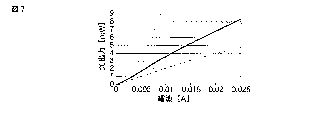
本実施形態で説明したGaN系青紫色LEDの発光特性を図7に示す。図7はLEDの注入電流に対する発光強度の関係を示している。図中において実線は本実施形態に係るGaN系青紫色LED、破線は従来構造のLEDの特性である。図示するように光出力は従来に比べ格段に向上し、注入電流値が20mAの時に、電圧4.3V、光出力6.9mW(発光波長λp=450nm)という結果が得られた。従来の電極構造では、同様の注入電流の時に得られる光出力は4.0mWであり、本発明の電極構造を採用することで光出力は従来構造に比して約1.7倍に向上し、発光の取り出し効率が改善されたことを明確に示している。 The emission characteristics of the GaN blue-violet LED described in this embodiment are shown in FIG. FIG. 7 shows the relationship of the light emission intensity to the injection current of the LED. In the figure, the solid line represents the characteristics of the GaN-based blue-violet LED according to the present embodiment, and the broken line represents the characteristics of the LED having the conventional structure. As shown in the figure, the light output is remarkably improved as compared with the conventional case, and when the injection current value is 20 mA, the voltage is 4.3 V and the light output is 6.9 mW (light emission wavelength λp = 450 nm). In the conventional electrode structure, the light output obtained at the same injection current is 4.0 mW, and by adopting the electrode structure of the present invention, the light output is improved by about 1.7 times compared to the conventional structure. This clearly shows that the emission extraction efficiency is improved.
また、室温において駆動電流20mAで動作させた際の光出力は、1000時間で80%まで低下したに過ぎず、LEDの信頼性が向上したことを証明する結果が得られている。 In addition, the light output when operated at a drive current of 20 mA at room temperature has only decreased to 80% in 1000 hours, and results have been proved that the reliability of the LED has been improved.
図8、図9にバリア電極、オーミック電極の膜厚に対する反射率Rの関係を示す。図8はオーミック電極(Ni層)の膜厚を4nm、高反射率電極(Al層)の膜厚を100nmとした時の、反射率のバリア電極(Mo層)膜厚依存性を示し、図9はバリア電極(Mo層)の膜厚を1nm、高反射電極(Al層)の膜厚を100nmとした時の、反射率のオーミック電極(Ni層)膜厚依存性を示している。 8 and 9 show the relationship of the reflectance R with respect to the film thickness of the barrier electrode and the ohmic electrode. FIG. 8 shows the dependence of the reflectivity on the barrier electrode (Mo layer) thickness when the thickness of the ohmic electrode (Ni layer) is 4 nm and the thickness of the high reflectivity electrode (Al layer) is 100 nm. 9 shows the dependence of the reflectance on the ohmic electrode (Ni layer) thickness when the thickness of the barrier electrode (Mo layer) is 1 nm and the thickness of the highly reflective electrode (Al layer) is 100 nm.
図示するように、反射率はバリア電極及びオーミック電極の膜厚に大きく依存し、その膜厚は薄い程好ましいことが分かる。特にInGaN活性層で発生した発光が最初に入射するオーミック電極の膜厚の制御が特に重要と言うことが出来、図9に示すように、オーミック電極にNiを用いる場合、その膜厚は10nm以下にすることが望ましい。 As shown in the figure, it can be seen that the reflectivity greatly depends on the film thickness of the barrier electrode and the ohmic electrode, and the thinner the film thickness, the better. In particular, it can be said that control of the thickness of the ohmic electrode on which light emitted from the InGaN active layer first enters is particularly important. As shown in FIG. 9, when Ni is used for the ohmic electrode, the thickness is 10 nm or less. It is desirable to make it.
なお、オーミック電極に使用する材料はNiの他に、Pt、Mg、Zn、Be、Ag、Au、Ge等を用いることが出来、これらの材料を主とする化合物でもかまわない。またバリア電極の材料はMoの他に、W、Pt、Ni、Ti、Pd、V等やそれらを主とする化合物を用いることが出来る。なお、NiとPtはオーミック電極とバリア電極とを兼用することが可能である。 In addition to Ni, Pt, Mg, Zn, Be, Ag, Au, Ge, etc. can be used as the material used for the ohmic electrode, and compounds mainly composed of these materials may be used. In addition to Mo, W, Pt, Ni, Ti, Pd, V, etc., and compounds mainly composed of them can be used as the material for the barrier electrode. Ni and Pt can be used both as an ohmic electrode and a barrier electrode.
また、上記オーミック電極、バリア電極、及び高反射電極上には、更にTi層35によるバリア電極及びAu層36によるオーバーコート電極とを設けている。通常、半導体発光素子を搭載するサブマウントにはAu等の導体パターンが形成されている。そしてこの導体パターン上に半導体発光素子の電極が接着されるが、Au等の導体パターン上にAlやAgなどの高反射率電極を直接接触させると、この接合面に高抵抗層が形成されたり、両者の接合が剥がれたりする問題があった。しかし、本実施形態では、導体パターンに用いているAuと同じ材料によるオーバーコート電極を設け、Au同士で接合部を形成している。そのため上記の問題を解決できる。更に、オーバーコート電極と高反射電極との間に高融点材料からなるバリア電極を介在させることにより、オーバーコート電極と導体パターンとの接合信頼性を向上している。但し、導体パターンと高反射率電極とが同じ材料である場合には、このオーバーコート電極及び高融点材料によるバリア電極は不要である。
Further, a barrier electrode made of the
なお、このバリア電極にはTiの他に、W、Mo、Pt、Ni、Ti、Pd、V等やそれらを主とする化合物を用いることが出来る。 For this barrier electrode, in addition to Ti, W, Mo, Pt, Ni, Ti, Pd, V, etc., and compounds mainly composed of them can be used.
また、半導体発光素子をリードフレームに直接接着するのではなく、導電性のサブマウントを介して接着することにより放熱効率を向上できるため、LEDの動作信頼性を更に向上できる。 In addition, since the heat radiation efficiency can be improved by bonding the semiconductor light emitting element directly to the lead frame via a conductive submount, the operational reliability of the LED can be further improved.
図10は本実施形態の変形例に係る半導体発光素子について説明するためのもので、赤色〜緑色で発光するGaAs、GaP系半導体発光素子の断面図である。 FIG. 10 is a cross-sectional view of a GaAs / GaP-based semiconductor light emitting element that emits red to green light for explaining a semiconductor light emitting element according to a modification of the present embodiment.
図示するように、n型GaP基板40上にn型InGaAlP接着層41、n型InGaAlPクラッド層42が形成され、このn型InGaAlPクラッド層42上にInGaAlP活性層43が形成されている。緑色の発光エネルギーに相当するバンドギャップエネルギーの得られる組成において間接遷移型のバンド構造を取るAlGaAsと異なり、InGaAlPは赤色〜緑色の発光が得られる組成において直接遷移型のバンド構造を有しており、この波長領域での発光デバイスに適した材料である。このInGaAlP活性層43上にp型InGaAlPクラッド層44、及びp型GaAsコンタクト層45が形成されている。そしてp型GaAsコンタクト層45上及びn型GaP基板40裏面にはそれぞれp型電極47、n型電極48が形成され、その他の領域を絶縁膜46が被覆している。p型電極47は、p型GaAsコンタクト層45とのオーミック接触の取れるのAuZn層49、バリア電極となるMo層50、高反射電極としてのAl層51、バリア電極となるTi層52、リードフレーム12上のサブマウント13との接触性を向上させるオーバーコート電極となるAu層53の5層構造を有している。
As shown, an n-type
上記構造の半導体発光素子が、図1に示したように、n型GaP基板40面を上にしてサブマウント13を介してリードフレーム12上に搭載されている。
As shown in FIG. 1, the semiconductor light emitting device having the above structure is mounted on the
なお、n型電極がn型GaP基板の裏面に設けられているため、n型電極とリードフレーム12との接続はワイヤボンディングにより行う必要がある。しかし、GaN系半導体発光素子で説明したように、p型電極が形成される面にn型InGaAlPクラッド層の一部露出される領域を設けて、該領域上にn型電極を形成することによりワイヤボンディングを必要としない構造としても良い。
Since the n-type electrode is provided on the back surface of the n-type GaP substrate, it is necessary to connect the n-type electrode and the
上記構成の半導体発光素子によれば、オーミック電極(AuZn層)と高反射率電極(Al層)との間に高融点金属のバリア電極(Mo層)を設けている。このバリア電極がオーミック電極及び高反射率電極を構成している金属原子の相互拡散を抑制するため、動作電圧の上昇を防止出来、上記GaN系半導体発光素子と同様の効果を得ることが出来る。 According to the semiconductor light emitting device having the above configuration, the refractory metal barrier electrode (Mo layer) is provided between the ohmic electrode (AuZn layer) and the high reflectivity electrode (Al layer). Since this barrier electrode suppresses interdiffusion of metal atoms constituting the ohmic electrode and the high reflectivity electrode, an increase in operating voltage can be prevented, and the same effect as that of the GaN-based semiconductor light emitting device can be obtained.
なお、p型電極47の製造方法は前述のGaN系半導体発光素子の場合と同様であるので説明は省略する。
Note that the manufacturing method of the p-
次にこの発明の第2の実施形態に係る半導体発光素子及び半導体発光装置について、GaN系青紫色LEDを例に挙げて図11を用いて説明する。図11は半導体発光素子11の構造について示している。
Next, a semiconductor light emitting element and a semiconductor light emitting device according to a second embodiment of the present invention will be described with reference to FIG. 11 taking a GaN blue-violet LED as an example. FIG. 11 shows the structure of the semiconductor
図示するように、本実施形態に係る半導体発光素子は第1の実施形態で説明した半導体発光素子11において、p型電極26の構造を変形したものである。すなわち、p型GaN層24と接するNi層32を島状に形成し、この島状のNi層32及びp型GaN層24上にMo層33を形成している。このためp型GaN層24の表面はNi層32に接する領域とMo層32に直接接する領域とを有することとなる。
As shown in the drawing, the semiconductor light emitting device according to the present embodiment is obtained by modifying the structure of the p-
そして、InGaN活性層22からp型AlGaNクラッド層23の方向へ放出されてp型電極26に到達した発光のうちの一部は、Ni層32及びMo層33を低散乱、低吸収で通過しAl層34で反射され、他方はNi層32を通らず直接Mo層33を通過してAl層34で反射する。
A part of the light emitted from the InGaN
上記構成によれば、p型GaN層24とオーミック接触をとるためのNi層をp型電極の全面に設けるのではなく、例えば島状の形状にしてp型GaN層24上の一部にのみ設けている。そのため、Ni層24の存在しない領域ではp型GaN層24と高反射電極であるAl層34との距離が小さくなるため、より反射率を向上できる。そのため、第1の実施形態で述べた効果と共に、更に発光の取り出し効率を向上できる。またNiとPtはオーミック電極とバリア電極とを兼用することが出来る。
According to the above configuration, the Ni layer for making ohmic contact with the p-
なお、オーミック接触をとるための電極材料、バリア電極の材料、及び高反射電極材料については、第1の実施形態で述べたものと同様の材料を用いることが出来る。また、本実施形態で説明した半導体発光素子を有するLEDの構造は、第1の実施形態で説明した図1と同様である。 As the electrode material for making ohmic contact, the material for the barrier electrode, and the highly reflective electrode material, the same materials as those described in the first embodiment can be used. The structure of the LED having the semiconductor light emitting element described in this embodiment is the same as that in FIG. 1 described in the first embodiment.
また、図12には本実施形態の変形例に係る半導体発光素子について示しておりGaAs、GaP系半導体発光素子の断面図である。 FIG. 12 shows a semiconductor light emitting device according to a modification of the present embodiment, and is a cross-sectional view of a GaAs, GaP semiconductor light emitting device.
図示するように、本変形例は第1の実施形態の変形例であるGaAs、GaP系半導体発光素子に本実施形態の電極構造を適用したものであり、同様の効果が得られる。 As shown in the figure, the present modification is an application of the electrode structure of the present embodiment to the GaAs and GaP-based semiconductor light-emitting elements that are modifications of the first embodiment, and the same effects can be obtained.
次にこの発明の第3の実施形態に係る半導体発光素子及び半導体発光装置についてGaN系半導体発光素子を例に挙げて図13を用いて説明する。図13は半導体発光素子の斜視図である。 Next, a semiconductor light-emitting device and a semiconductor light-emitting device according to a third embodiment of the present invention will be described with reference to FIG. 13 taking a GaN-based semiconductor light-emitting device as an example. FIG. 13 is a perspective view of a semiconductor light emitting device.
図示するように、サファイア基板20上にn型GaN層21及び発光層55が設けられている。発光層55は第1、第2実施形態で説明したように、n型GaN層21上に設けられたInGaN活性層22、InGaN活性層22上のp型AlGaNクラッド層23及びp型GaN層24である。そしてチップの周辺領域におけるn型GaN層21及び発光層55が除去されてn型GaN層21の表面が露出している。更に発光層55上にはやはり第1、第2の実施形態で述べたオーミック電極32、電極33、高反射率電極34、バリア電極35及びオーバーコート電極36からなるp型電極26が設けられている。このp型電極26は発光層55上の略中央に配置されている。一方、n型電極25は、露出されたn型GaN層21上に、発光層55を取り囲むようにして設けられている。
As shown in the figure, an n-
そして、上記構成の半導体発光素子が、図1のようにサブマウントを介してリードフレーム上に搭載されてLEDが形成される。 Then, the semiconductor light emitting device having the above-described configuration is mounted on a lead frame via a submount as shown in FIG. 1 to form an LED.
上記のような電極配置を有する半導体発光素子であると、第1、第2の実施形態で説明した効果に加えて次のような効果が合わせて得られる。まず第1にp型電極がチップの略中央に配置されていることにより、サブマウント13に半導体発光素子をマウントする際のp型電極26の位置決めを容易にする事が出来、LEDの製造を容易とし、スループットを向上できる。
In addition to the effects described in the first and second embodiments, the following effects can be obtained in combination with the semiconductor light emitting device having the electrode arrangement as described above. First, since the p-type electrode is arranged at the approximate center of the chip, the positioning of the p-
第2にn型電極25が発光層55の周辺を取り囲むようにして配置されているため、p型電極26から注入された電流が均一に活性層に注入されるため、効率の良い発光が得られる。
Secondly, since the n-
なお本実施形態ではn型電極55の一部が除去されているが、これは半導体発光素子をサブマウントにマウントする際にp型電極に接続する導体パターンの形成領域に対応して設けたものである。
In this embodiment, a part of the n-
本実施形態の変形例に係る半導体発光素子及び半導体発光装置について図14を用いて説明する。図14は半導体発光素子の斜視図である。 A semiconductor light emitting element and a semiconductor light emitting device according to a modification of the present embodiment will be described with reference to FIG. FIG. 14 is a perspective view of the semiconductor light emitting device.
図示するように、本変形例は図14で説明した半導体発光素子において、p型電極26を形成した発光層55以外の領域の殆どを除去したものである。上記構成では発光領域が限定されるため、発光が光ファイバ等との結合が必要な場合や、より高速動作が必要とされるLEDに適した構造である。
As shown in the figure, this modification is obtained by removing most of the region other than the
上記第3の実施形態及び変形例において、発光層55、p型電極、及びn型電極の形状は図示した形状に限られるものではないし、GaN系半導体発光素子のみならず、GaAs、GaP系半導体発光素子にも適用できることは言うまでもない。また、導電基板を用いる場合にはn型電極を基板裏面に設けてもかまわないことは勿論である。
In the third embodiment and the modification, the shapes of the
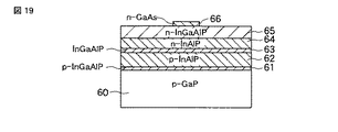
次にこの発明の第4の実施形態に係る半導体発光素子とその製造方法、及び半導体発光装置についてGaAs、GaP系半導体発光素子を例に挙げて説明する。図15は発光波長620nmの赤色光を発生する半導体発光素子の断面図である。 Next, a semiconductor light emitting device, a method for manufacturing the same, and a semiconductor light emitting device according to a fourth embodiment of the present invention will be described by taking GaAs and GaP semiconductor light emitting devices as examples. FIG. 15 is a cross-sectional view of a semiconductor light emitting device that emits red light having an emission wavelength of 620 nm.
図示するように、p型GaP基板60上にp型InGaAlP接着層61、p型InAlPクラッド層62が形成され、p型InAlPクラッド層62上にはInGaAlP活性層63が形成されている。このInGaAlP活性層63上にはn型InAlPクラッド層64及びn型InGaAlP窓層65が形成されている。そしてn型InGaAlP窓層65上にはn型GaAsコンタクト層66を介してn型電極67が設けられている。一方、p型GaP基板60裏面にはp型電極68及び光反射膜69とが設けられている。
As shown in the figure, a p-type
上記半導体発光素子の製造方法について、図16乃至図19を用いて説明する。図16乃至図19はそれぞれ半導体発光素子の製造工程の断面図を順次示している。 A method for manufacturing the semiconductor light emitting device will be described with reference to FIGS. 16 to 19 sequentially show cross-sectional views of the manufacturing process of the semiconductor light emitting device.
まず図16に示すように、n型GaAs基板70上にMO−CVD法等によりInGaP等によるエッチングストップ層71、膜厚0.1μmのn型GaAsコンタクト層66、膜厚0.5μmのn型In0.5Ga0.15Al0.35P窓層65及び膜厚1μmのn型In0.5Al0.5Pクラッド層64を順次形成する。次にn型InAlPクラッド層64上にMO−CVD法やMBE法等により0.2μmのアンドープIn0.5Ga0.1Al0.4P活性層63を形成し、その上に膜厚1μmのp型In0.5Al0.5Pクラッド層62及び膜厚0.05μmのp型In0.5Ga0.15Al0.35P接着層61を形成する。また、各層のエピタキシャル成長において、ガリウム原料にはトリエチルガリウム(TEG:triethylgallium, Ga(C2H5)3)やトリメチルガリウム(TMG:trimethylgallium, Ga(CH3)3)を、アルミニウム原料にはトリエチルアルミニウム(TEA:triethylaluminium, Al(C2H5)3)やトリメチルアルミニウム(TMA:trimethylaluminium, [Al(CH3)3]2)を、インジウム原料にはトリエチルインジウム(TEI:triethylindium, In(C2H5)3)やトリメチルインジウム(TMI:trimethylindium, In(CH3)3)を、リン原料にはターシャリブチルホスフィン(TBP:tertiary-butylphosphine, C4H9PH2)等を用いる。またn型不純物及びp型不純物にはそれぞれSi及びZnを用いているが、TeやBe等も使用可能である。
First, as shown in FIG. 16, an
なお、上記各層の組成及び膜厚は、発光波長620nmの赤色発光を得る際に用いる一例であって、具体的な原料も一例に過ぎない。 In addition, the composition and film thickness of each of the above layers are examples used for obtaining red light emission having an emission wavelength of 620 nm, and specific raw materials are only examples.
次に図17に示すように、p型InGaAlP接着層61上に、厚さ200μmのp型GaP基板60を加熱圧着により接着する。この際、p型InGaAlP接着層61及びp型GaP基板60の相互の接着面を洗浄しておく必要がある。前述の通り、GaP基板は波長620nmの光に対しては透明な材料である。
Next, as shown in FIG. 17, a p-
次にn型GaAs基板70からエッチングストップ層71までのエッチングを行い、n型GaAs基板70を除去する。
Next, etching from the n-
そして図18に示すように、エッチングストップ層71を更に除去して、n型GaAsコンタクト層66をリソグラフィ技術とエッチングにより図のようにパターニングする。
Then, as shown in FIG. 18, the
その後はn型GaAsコンタクト層66上にn型電極67を、p型GaP基板70の裏面にはp型電極68及び光反射膜69をそれぞれ形成して図15の構造の半導体発光素子を完成する。なお、光反射膜69の材料にはAuを用いている。
Thereafter, an n-
そして第1の実施形態で説明したように、上記半導体発光素子をp型GaP60基板を下にしてリードフレームに搭載し、且つ電気的に接続した後にエポキシ樹脂でランプ化してLEDを完成する。 Then, as described in the first embodiment, the semiconductor light emitting device is mounted on a lead frame with the p-type GaP60 substrate facing down, electrically connected, and then ramped with epoxy resin to complete the LED.
上記構成のLEDにおいて、リードフレームから電圧が印加されてp型電極69から注入された電流はInGaAlP活性層63へ注入され、赤色の発光が得られる。InGaAlP活性層63で放出された波長620nmの赤色発光は、n型層側へ放出されたものはそのままn型InAlPクラッド層64及びn型InGaAlP窓層65を通過して半導体発光素子外部へ取り出される。一方、InGaAlP活性層63からp型GaP基板60側へ放出された発光は、透明基板であるp型GaP基板60を透過してp型電極68及び光反射膜69に到達する。到達した発光のうち、p型電極68では散乱及び吸収されてしまうが、光反射膜69では再び半導体発光素子内部へ反射されて、n型InGaAlP窓層65側から取り出される。この結果、駆動電流20mAの条件下で動作させた、放射角10°のパッケージにおいて、光出力は従来構造における光出力の1.2倍に相当する17cdが得られた。
In the LED having the above configuration, a current applied from the p-
上記のような構成の半導体発光素子によれば、フリップチップ構造を有するGaAs、GaP系半導体発光素子において、発光を反射させる透明基板の裏面の一部を光反射膜に置き換えている。そのため、透明基板と電極との間のアロイ層にて生じる損失を光反射膜を設けた分だけ低減でき、且つ光反射膜を設けた領域では高効率で発光を反射できるため、効率的に発光を半導体発光素子外部へ取り出すことが可能である。 According to the semiconductor light emitting device having the above configuration, in the GaAs / GaP semiconductor light emitting device having the flip chip structure, a part of the back surface of the transparent substrate that reflects light emission is replaced with a light reflecting film. Therefore, the loss generated in the alloy layer between the transparent substrate and the electrode can be reduced by the amount of the light reflection film provided, and the light emission can be reflected with high efficiency in the area where the light reflection film is provided. Can be taken out of the semiconductor light emitting device.
なお、本実施形態では光反射膜69の材料にはAuを用いている。これはInGaAlP活性層63による波長620nmの発光に対して大きな反射率を有しているからである。表1に各種金属材料のGaP接合における反射率R及び熱伝導率kについて示す。反射率は波長620nmの光に対する数値であり、この波長でのGaPの屈折率nは3.325である。また熱伝導率は温度300Kにおける数値である。
光反射膜69に求められる特性としては、高反射率はもとより高熱伝導率を有することが望ましい。InGaAlP系の材料は熱による発光効率の低下が顕著であり、活性層付近の発熱を効率よく素子外部へ放熱する必要があるためである。そのため表1から明らかなように、高反射率及び高熱伝導率を両立できる材料として、Auの他にAg、Cu、Al等を用いることが好ましい。
As a characteristic required for the
また、p型GaP基板60の裏面に設けたp型電極68及び光反射膜69において、光反射膜69による発光の反射効果と電流注入用電極部のコンタクト抵抗との間にはトレードオフの関係があり、適宜必要十分な面積比とする必要がある。本実施形態では光反射膜69とp型電極68との面積比を1:1にしているが、当然ながら光反射膜69の面積を大きくすることにより発光の取り出し効率が向上することから、コンタクト抵抗の上昇が顕著な問題とならない範囲で光反射膜69の面積を可能な限り大きくすることが望ましい。
Further, in the p-
次に本実施形態の変形例について図20を用いて説明する。図20は図15において、特に光反射膜69の構造に着目した半導体発光素子の断面図である。
Next, a modification of this embodiment will be described with reference to FIG. FIG. 20 is a cross-sectional view of the semiconductor light emitting element in FIG. 15 with particular attention paid to the structure of the
図示するように、p型GaP基板60の裏面に設けられた光反射膜69は、Si層72とAl2O3層73による多層構造を成しており、それぞれの膜厚は、活性層での発光波長λに対してλ/4n(nは当該発光波長におけるSi及びAl2O3の屈折率)になるよう設定されている。
As shown in the figure, the
Si層72とAl2O3層73との組み合わせはその屈折率差が大きく、且つ高屈折率層であるSi層72の吸収係数が小さいことから、少ない対数で高い反射率を得ることが可能である。しかし、低屈折率層であるAl2O3層73は熱伝導率が小さく、素子の熱特性を劣化させる可能性がある。
The combination of the
図21に本実施形態、本実施形態の変形例、及び従来構造のLEDの注入電流に対する光出力の特性を示す。図21の図中において、(1)乃至(3)のラインがそれぞれ図15、図20、及び従来構造のLEDの特性を示している。 FIG. 21 shows the characteristics of the light output with respect to the injection current of the present embodiment, a modification of the present embodiment, and the LED of the conventional structure. In FIG. 21, the lines (1) to (3) indicate the characteristics of the LEDs of FIGS. 15 and 20 and the conventional structure, respectively.
図示するように、図15に示す構造が出力、耐久性共に最も優れている。一方で本実施形態の変形例で説明した図20の構造では、Al2O3の低熱伝導率の影響により注入電流が大きくなった際に光出力が飽和しつつある様子が分かる。しかし、それでも注入電流〜150mAの全測定範囲において従来構造の光出力を上回っており、通常の動作電流として使用される20mAの条件ではほぼ図15の構造と同等の特性を有しており、本変形例の構造を有する半導体発光素子をLEDに用いることは十分に利点があると言える。 As shown in the figure, the structure shown in FIG. 15 is most excellent in output and durability. On the other hand, in the structure of FIG. 20 described in the modification of the present embodiment, it can be seen that the light output is being saturated when the injection current increases due to the low thermal conductivity of Al 2 O 3 . However, it still exceeds the light output of the conventional structure in the entire measurement range of injection current to 150 mA, and has almost the same characteristics as the structure of FIG. 15 under the condition of 20 mA used as a normal operating current. It can be said that it is sufficiently advantageous to use a semiconductor light emitting element having a modified structure for an LED.
次にこの発明の第5の実施形態に係る半導体発光素子及びその製造方法についてGaAs、GaP系半導体発光素子を例に挙げて説明する。図22は発光波長620nmの赤色光を発生する半導体発光素子の断面図である。 Next, a semiconductor light emitting device and a method for manufacturing the same according to a fifth embodiment of the present invention will be described by taking GaAs and GaP semiconductor light emitting devices as examples. FIG. 22 is a cross-sectional view of a semiconductor light emitting device that emits red light having an emission wavelength of 620 nm.
図示するように、n型GaP基板80上の一部に発光層81が形成されている。発光層81は、n型InGaAlPコンタクト層82、n型InAlPクラッド層83、InGaAlP活性層84、p型InAlPクラッド層85、及びp型InGaAlPコンタクト層86の多層構造を成している。また、n型GaP基板80上の発光層81の形成されていない領域は、アンドープのGaP電流狭窄層87が形成され、全面をp型GaP層88が被覆している。そして、p型GaP層88上の一部にはp型電極89が形成され、n型GaP基板80の裏面にはn型電極90及び光反射膜91が形成されている。なお、n型電極90は、発光層81の直下に位置するように配置されている。
As shown in the drawing, a
次に上記構成の半導体発光素子の製造方法について図23乃至図28を用いて説明する。図23乃至図28は、半導体発光素子の製造工程の断面図を順次示している。 Next, a method for manufacturing the semiconductor light emitting device having the above structure will be described with reference to FIGS. 23 to 28 sequentially show cross-sectional views of the manufacturing process of the semiconductor light emitting device.
まず図23に示すように、n型GaAs基板92上にn型In0.5Ga0.15Al0.35Pコンタクト層82、n型In0.5Al0.5Pクラッド層83、In0.5Ga0.1Al0.4P活性層84、p型In0.5Al0.5Pクラッド層85及びp型In0.5Ga0.15Al0.35Pコンタクト層86を順次形成する。なお各層は第4の実施形態と同様の方法により成長を行う。次に、同じくMO−CVD法等によりアンドープのGaAs保護層93及びSiO2マスク層94を順次形成する。
First, as shown in FIG. 23, an n-type In 0.5 Ga 0.15 Al 0.35
次に図24に示すように、リソグラフィ技術とウェットエッチング法等により、SiO2マスク層94をパターニングする。そしてSiO2マスク層94をマスクに用いたRIE法によりGaAs保護層93、p型In0.5Ga0.15Al0.35Pコンタクト層86、p型In0.5Al0.5Pクラッド層85、In0.5Ga0.1Al0.4P活性層84、n型In0.5Al0.5Pクラッド層83及びn型In0.5Ga0.15Al0.35Pコンタクト層82を図のようにエッチングしてリッジ形状とする。
Next, as shown in FIG. 24, the SiO 2 mask layer 94 is patterned by a lithography technique and a wet etching method. Then, the GaAs
次に図25に示すように、n型GaAs基板92上にアンドープのGaP電流狭窄層87をCVD法等により選択的にエピタキシャル成長する。
Next, as shown in FIG. 25, an undoped GaP
引き続き図26に示すように、全面にp型GaP層88を形成する。
Subsequently, as shown in FIG. 26, a p-
そして図27に示すように、n型GaAs基板92をエッチングにより全て除去した後、図28のようにn型GaP基板80を接合する。
Then, as shown in FIG. 27, after all the n-
その後はp型GaP層88上にp型電極89を形成し、またn型GaP基板80の裏面にはn型電極90及び光反射膜90を形成し、図22の構造の半導体発光素子を完成する。
Thereafter, a p-
なお発光層81をn型GaAs基板上の一部にのみ残存させ、最終的に発光層81の周辺を全てGaPにより取り囲む構造とするのが望ましい。
It is desirable that the
上記半導体発光素子において、InGaAlP活性層84より放出された赤色発光のうち、p型層側へ放出されたものはそのままp型InAlPクラッド層85及びp型InGaAlPコンタクト層86及びp型GaP層88を通過して半導体発光素子外部へ取り出される。一方、InGaAlP活性層84からn型GaP基板80側へ放出された発光は、透明基板であるp型GaP基板80を透過して光反射膜91で反射されて半導体発光素子外部に取り出される。
In the semiconductor light emitting device, among the red light emitted from the InGaAlP
ここで、n型電極90はInGaAlP活性層83の直下に設けられ、GaP電流狭窄層87直下に光反射膜91が設けられている。すなわち光反射膜87で反射された発光は発光層81を通らずに、バンドギャップエネルギーが発光エネルギーより大きいGaP電流狭窄層87を通って素子外部に取り出される。そのため、発光が発光層81を通過する際の再吸収が起こらないために、第4の実施形態で説明した構造に比べて発光の取り出し効率を更に向上できる。事実、駆動電流20mAの条件下で動作させた放射角10°のパッケージにおいて、光出力は従来構造における光出力の1.4倍に相当する20cdが得られた。
Here, the n-
上記第1乃至第3の実施形態によれば、活性層から放出された発光を発光層側の電極で反射させて基板側から発光を外部に取り出す、3−5族化合物半導体を用いた可視光半導体発光素子において、発光を反射させる電極構造を、少なくともオーミック電極、バリア電極、及び高反射電極の3層構造としている。このバリア電極は高融点材料で形成され、オーミック電極と高反射率電極とを構成する原子の熱による相互拡散を防止する役目をしている。更に膜厚を非常に小さくすることにより、オーミック電極及びバリア電極での発光の吸収損失を最小限に抑えている。そのため電極における、オーミック接触性と発光の高反射率とを両立しつつ、且つ熱による動作電圧の上昇を抑えることが出来、半導体発光素子及び半導体発光装置の信頼性及び性能を向上できる。また、オーミック電極を例えば島状に形成してその面積を小さくすることにより、発光のオーミック電極での損失を低減できるため、更に電極における反射率を大きくでき、発光の取り出し効率を更に向上できる。 According to the first to third embodiments, visible light using a Group 3-5 compound semiconductor, in which the light emitted from the active layer is reflected by the electrode on the light emitting layer side to extract the light emitted from the substrate side to the outside. In the semiconductor light emitting device, the electrode structure for reflecting light emission has a three-layer structure of at least an ohmic electrode, a barrier electrode, and a highly reflective electrode. This barrier electrode is formed of a high melting point material, and serves to prevent mutual diffusion of atoms constituting the ohmic electrode and the high reflectivity electrode due to heat. Furthermore, by making the film thickness very small, the absorption loss of light emission at the ohmic electrode and the barrier electrode is minimized. Therefore, the ohmic contact property and the high reflectance of light emission in the electrode can be compatible, and an increase in operating voltage due to heat can be suppressed, and the reliability and performance of the semiconductor light emitting element and the semiconductor light emitting device can be improved. Further, by forming the ohmic electrode in, for example, an island shape and reducing its area, the loss of the emitted ohmic electrode can be reduced, so that the reflectance at the electrode can be further increased and the emission extraction efficiency can be further improved.
また、上記第4、第5の実施形態によれば、活性層から放出された発光を基板側で反射させて発光層側から発光を外部に取り出す、GaAsやGaP等の、5族にN以外のAsやPを用いた3−5族化合物半導体による可視光半導体発光素子において、発光を反射させる半導体基板の裏面の同一面上に、一方の電極と光反射膜とを設けている。この電極においては発光は散乱、吸収が生じるるものの、光反射膜を設けた領域では高効率で発光が反射されるため、従来に比べて発光の外部への取り出し効率を向上できるので、半導体発光素子及び半導体発光装置の性能を向上できる。また、発光層をリッジ形状としてその周辺領域を発光に対して透明な材料で埋め込み、且つ半導体基板の裏面の電極を発光の直下に位置するように設けることで、光反射膜で反射される発光の再吸収を防止できるため、更に発光の取り出し効率を向上できる。 Further, according to the fourth and fifth embodiments, the light emitted from the active layer is reflected on the substrate side and the light emitted from the light emitting layer side is extracted to the outside. In the visible light semiconductor light emitting device using a group 3-5 compound semiconductor using As or P, one electrode and a light reflecting film are provided on the same surface of the back surface of the semiconductor substrate that reflects light. Although light is scattered and absorbed in this electrode, the light emission is reflected with high efficiency in the region where the light reflecting film is provided. The performance of the element and the semiconductor light emitting device can be improved. In addition, the light emitting layer is formed in a ridge shape and the peripheral region thereof is embedded with a material transparent to light emission, and the electrode on the back surface of the semiconductor substrate is provided so as to be positioned directly under the light emission, so that the light emission reflected by the light reflecting film Therefore, it is possible to further improve the light emission extraction efficiency.
なお、本願発明は上記実施形態に限定されるものではなく、実施段階ではその要旨を逸脱しない範囲で種々に変形することが可能である。更に、上記実施形態には種々の段階の発明が含まれており、開示される複数の構成要件における適宜な組み合わせにより種々の発明が抽出されうる。例えば、実施形態に示される全構成要件からいくつかの構成要件が削除されても、発明が解決しようとする課題の欄で述べた課題が解決でき、発明の効果の欄で述べられている効果が得られる場合には、この構成要件が削除された構成が発明として抽出されうる。 Note that the present invention is not limited to the above-described embodiment, and various modifications can be made without departing from the scope of the invention in the implementation stage. Furthermore, the above embodiments include inventions at various stages, and various inventions can be extracted by appropriately combining a plurality of disclosed constituent elements. For example, even if some constituent requirements are deleted from all the constituent requirements shown in the embodiment, the problem described in the column of the problem to be solved by the invention can be solved, and the effect described in the column of the effect of the invention Can be extracted as an invention.
10…LED
11…半導体発光素子(半導体チップ)
12…リードフレーム
13…サブマウント
14…オーミック電極
15…ボンディングワイヤ
16…導電ペースト
17…AuSn
18…エポキシ樹脂
19…絶縁膜
20、200…サファイア基板
21、210…n型GaN層
22…InGaN活性層
23…p型AlGaN層
24、220…p型GaN層
25、48、67、90、230、380、460、470…n型電極
26、47、68、89、240、250、260、370、480…p型電極
27、46…絶縁膜
28、30、35、52…Ti層
29、34、51…Al層
31、36、53…Au層
32…Ni層
33、50…Mo層
40…n型GaP基板
41、42、65、82、320、440…n型InGaAlP層
43、63、84、330、430…InGaAlP活性層
44、61、86、340、410、420…p型InGaAlP層
45、360…p型GaAs層
49…AuZn層
55、81…発光層
60、400…p型GaP基板
62、85…p型InAlP層
64、83…n型InAlP層
66、310…n型GaAs層
69、91…高反射膜
70、92、300…n型GaAs基板
71…エッチングストップ層
72…Si層
73…Al2O3層
80…n型GaP基板
87…アンドープGaP層
88…p型GaP層
93…GaAs層
94…SiO2層
350…p型AlGaAs層
450…n型AlGaAs層
10 ... LED
11 ... Semiconductor light emitting device (semiconductor chip)
DESCRIPTION OF
18 ...
Claims (6)
前記第1半導体層上に設けられ、自然放出光を発生して放出する活性層と、
前記活性層上に設けられた第2導電型の第2半導体層と、
前記半導体基板上に、少なくとも前記第1、第2半導体層及び前記活性層の側面を取り囲むようにして設けられた電流狭窄層と、
前記第2半導体層及び前記電流狭窄層上に設けられた第3半導体層と、
前記半導体基板の裏面の一部に設けられた第1電極と、
前記半導体基板の裏面の前記第1電極と同一面上に設けられ、前記第1電極よりも高反射率の光反射膜と、
前記第3半導体層上に設けられた第2電極と
を具備し、前記活性層から前記第2半導体層側へ放出された発光は該第2半導体層を透過して外部へ取り出され、
前記活性層から前記第1半導体層側へ放出された発光は前記半導体基板を透過して前記光反射膜で反射されて前記第2半導体層側から取り出され、
前記第1電極は前記半導体基板の裏面において、前記活性層の直下の領域に設けられ、該半導体基板の裏面のその他の領域には前記光反射膜が設けられ、
前記光反射膜で反射された発光は、前記電流狭窄層を透過して外部へ取り出される
ことを特徴とする半導体発光素子。 A first semiconductor layer of a first conductivity type provided only on a part of a substantially transparent semiconductor substrate;
An active layer provided on the first semiconductor layer for generating and emitting spontaneously emitted light;
A second semiconductor layer of a second conductivity type provided on the active layer;
A current confinement layer provided on the semiconductor substrate so as to surround at least side surfaces of the first and second semiconductor layers and the active layer;
A third semiconductor layer provided on the second semiconductor layer and the current confinement layer;
A first electrode provided on a part of the back surface of the semiconductor substrate;
A light reflecting film provided on the same surface as the first electrode on the back surface of the semiconductor substrate, and having a higher reflectance than the first electrode;
A second electrode provided on the third semiconductor layer, and emitted light emitted from the active layer to the second semiconductor layer side is transmitted through the second semiconductor layer and extracted outside,
Light emitted from the active layer to the first semiconductor layer side is transmitted through the semiconductor substrate, reflected by the light reflecting film, and taken out from the second semiconductor layer side ,
The first electrode is provided in a region immediately below the active layer on the back surface of the semiconductor substrate, and the light reflecting film is provided in another region on the back surface of the semiconductor substrate,
The semiconductor light emitting device , wherein the light emitted from the light reflecting film is extracted outside through the current confinement layer .
ことを特徴とする請求項1記載の半導体発光素子。 The light reflective film according to claim 1 Symbol mounting the semiconductor light emitting element, characterized in that it is made of a material mainly containing at least a metal.
ことを特徴とする請求項1記載の半導体発光素子。 The light reflective film according to claim 1 Symbol mounting the semiconductor light emitting element, characterized in that it is made of a material mainly containing at least a dielectric.
前記高屈折率膜よりも屈折率の低い低屈折率膜との多層構造を有する
ことを特徴とする請求項1記載の半導体発光素子。 The light reflecting film is at least a high refractive index film having a higher refractive index than the semiconductor substrate;
Claim 1 Symbol mounting the semiconductor light emitting device characterized by having a multi-layer structure and the high refractive index film having a refractive index lower than that of the low refractive index film.
ことを特徴とする請求項1乃至4いずれか1項記載の半導体発光素子。 The first and second semiconductor layers and the active layer are made of a mixed crystal of two or more materials of a group consisting of InP, GaP, AlP, and GaAs materials. 4. The semiconductor light emitting device according to any one of 4 above.
前記リードフレーム上に設けられ、該リードフレームと電気的に接続された導電性のサブマウントと、
前記サブマウント上に半導体基板を下にして設けられ、前記サブマウントと電気的に接続された半導体発光素子と、
少なくとも前記サブマウント及び前記半導体発光素子を被覆する保護部材と
を具備し、前記半導体発光素子は、
実質的に透明な半導体基板上の一部にのみ設けられた第1導電型の第1半導体層と、
前記第1半導体層上に設けられ、自然放出光を発生して放出する活性層と、
前記活性層上に設けられた第2導電型の第2半導体層と、
前記半導体基板上に、少なくとも前記第1、第2半導体層及び前記活性層の側面を取り囲むようにして設けられた電流狭窄層と、
前記第2半導体層及び前記電流狭窄層上に設けられた第3半導体層と、
前記半導体基板の裏面の一部に設けられた第1電極と、
前記半導体基板の裏面の前記第1電極と同一面上に設けられ、前記第1電極よりも高反射率の光反射膜と、
前記第3半導体層上に設けられた第2電極と
を具備し、前記活性層から前記第2半導体層側へ放出された発光は該第2半導体層を透過して外部へ取り出され、
前記活性層から前記第1半導体層側へ放出された発光は前記半導体基板を透過して前記光反射膜で反射されて前記第2半導体層側から取り出され、
前記第1電極は前記半導体基板の裏面において、前記活性層の直下の領域に設けられ、該半導体基板の裏面のその他の領域には前記光反射膜が設けられ、
前記光反射膜で反射された発光は、前記電流狭窄層を透過して外部へ取り出される
ことを特徴とする半導体発光装置。 A lead frame that exchanges power with the outside,
A conductive submount provided on the lead frame and electrically connected to the lead frame;
A semiconductor light emitting device provided on the submount with a semiconductor substrate facing down and electrically connected to the submount;
A protective member covering at least the submount and the semiconductor light emitting element, and the semiconductor light emitting element comprises:
A first semiconductor layer of a first conductivity type provided only on a part of a substantially transparent semiconductor substrate;
An active layer provided on the first semiconductor layer for generating and emitting spontaneously emitted light;
A second semiconductor layer of a second conductivity type provided on the active layer;
A current confinement layer provided on the semiconductor substrate so as to surround at least side surfaces of the first and second semiconductor layers and the active layer;
A third semiconductor layer provided on the second semiconductor layer and the current confinement layer;
A first electrode provided on a part of the back surface of the semiconductor substrate;
A light reflecting film provided on the same surface as the first electrode on the back surface of the semiconductor substrate, and having a higher reflectance than the first electrode;
A second electrode provided on the third semiconductor layer, and emitted light emitted from the active layer to the second semiconductor layer side is transmitted through the second semiconductor layer and extracted outside,
Light emitted from the active layer to the first semiconductor layer side is transmitted through the semiconductor substrate, reflected by the light reflecting film, and taken out from the second semiconductor layer side ,
The first electrode is provided in a region immediately below the active layer on the back surface of the semiconductor substrate, and the light reflecting film is provided in another region on the back surface of the semiconductor substrate,
Light emission reflected by the light reflecting film is transmitted through the current confinement layer and extracted outside .
Priority Applications (1)
| Application Number | Priority Date | Filing Date | Title |
|---|---|---|---|
| JP2007148137A JP4625827B2 (en) | 2007-06-04 | 2007-06-04 | Semiconductor light emitting device and semiconductor light emitting device |
Applications Claiming Priority (1)
| Application Number | Priority Date | Filing Date | Title |
|---|---|---|---|
| JP2007148137A JP4625827B2 (en) | 2007-06-04 | 2007-06-04 | Semiconductor light emitting device and semiconductor light emitting device |
Related Parent Applications (1)
| Application Number | Title | Priority Date | Filing Date |
|---|---|---|---|
| JP2000200298A Division JP4024994B2 (en) | 2000-06-30 | 2000-06-30 | Semiconductor light emitting device |
Publications (2)
| Publication Number | Publication Date |
|---|---|
| JP2007221175A JP2007221175A (en) | 2007-08-30 |
| JP4625827B2 true JP4625827B2 (en) | 2011-02-02 |
Family
ID=38498033
Family Applications (1)
| Application Number | Title | Priority Date | Filing Date |
|---|---|---|---|
| JP2007148137A Expired - Fee Related JP4625827B2 (en) | 2007-06-04 | 2007-06-04 | Semiconductor light emitting device and semiconductor light emitting device |
Country Status (1)
| Country | Link |
|---|---|
| JP (1) | JP4625827B2 (en) |
Families Citing this family (5)
| Publication number | Priority date | Publication date | Assignee | Title |
|---|---|---|---|---|
| JP2009088160A (en) * | 2007-09-28 | 2009-04-23 | Dowa Electronics Materials Co Ltd | Light emitting diode and manufacturing method thereof |
| JP2011515859A (en) * | 2008-03-26 | 2011-05-19 | ラティス パワー (チアンシ) コーポレイション | Semiconductor light-emitting device with highly reflective ohmic electrodes |
| JP5324116B2 (en) * | 2008-03-28 | 2013-10-23 | 京セラ株式会社 | Light emitting device and manufacturing method thereof |
| DE102010024079B4 (en) | 2010-06-17 | 2025-08-28 | OSRAM Opto Semiconductors Gesellschaft mit beschränkter Haftung | Method for producing an optoelectronic semiconductor chip and optoelectronic semiconductor chip |
| KR20140059985A (en) * | 2012-11-09 | 2014-05-19 | 엘지이노텍 주식회사 | Light emitting device |
Family Cites Families (8)
| Publication number | Priority date | Publication date | Assignee | Title |
|---|---|---|---|---|
| JPS49149679U (en) * | 1973-04-27 | 1974-12-25 | ||
| JPH0488684A (en) * | 1990-08-01 | 1992-03-23 | Koito Mfg Co Ltd | Led chip electrode structure |
| JPH0645651A (en) * | 1992-05-22 | 1994-02-18 | Sanyo Electric Co Ltd | Electrode for n-type sic and its formation |
| JPH0690021A (en) * | 1992-09-08 | 1994-03-29 | Sharp Corp | Pn junction type light emitting diode using silicon carbide |
| JPH0722646A (en) * | 1993-06-30 | 1995-01-24 | Mitsubishi Chem Corp | LED with current blocking layer |
| US5917202A (en) * | 1995-12-21 | 1999-06-29 | Hewlett-Packard Company | Highly reflective contacts for light emitting semiconductor devices |
| JP3130292B2 (en) * | 1997-10-14 | 2001-01-31 | 松下電子工業株式会社 | Semiconductor light emitting device and method of manufacturing the same |
| JPH11186613A (en) * | 1997-12-19 | 1999-07-09 | Matsushita Electron Corp | Semiconductor light emitting device |
-
2007
- 2007-06-04 JP JP2007148137A patent/JP4625827B2/en not_active Expired - Fee Related
Also Published As
| Publication number | Publication date |
|---|---|
| JP2007221175A (en) | 2007-08-30 |
Similar Documents
| Publication | Publication Date | Title |
|---|---|---|
| JP4024994B2 (en) | Semiconductor light emitting device | |
| US9472713B2 (en) | Semiconductor light-emitting device | |
| US6838704B2 (en) | Light emitting diode and method of making the same | |
| CN101673794B (en) | Light emitting device | |
| JP5276959B2 (en) | LIGHT EMITTING DIODE, ITS MANUFACTURING METHOD, AND LAMP | |
| JP4644193B2 (en) | Semiconductor light emitting device | |
| CN102969414A (en) | Semiconductor light emitting element | |
| JP2012074665A (en) | Light-emitting diode | |
| JP4625827B2 (en) | Semiconductor light emitting device and semiconductor light emitting device | |
| KR20120002130A (en) | Flip chip type light emitting device and manufacturing method thereof | |
| KR20150062179A (en) | Light emitting diode having enlarged reflecting layer | |
| JP5682427B2 (en) | Light emitting element | |
| JP2010186808A (en) | Light-emitting diode and light-emitting diode lamp | |
| JP2003031852A (en) | Semiconductor light emitting device and method of manufacturing the same | |
| CN118943266A (en) | Light emitting diode and light emitting device | |
| JP2009200227A (en) | Light-emitting element and lighting device |
Legal Events
| Date | Code | Title | Description |
|---|---|---|---|
| A621 | Written request for application examination |
Free format text: JAPANESE INTERMEDIATE CODE: A621 Effective date: 20070604 |
|
| A131 | Notification of reasons for refusal |
Free format text: JAPANESE INTERMEDIATE CODE: A131 Effective date: 20100406 |
|
| A521 | Request for written amendment filed |
Free format text: JAPANESE INTERMEDIATE CODE: A523 Effective date: 20100519 |
|
| TRDD | Decision of grant or rejection written | ||
| A01 | Written decision to grant a patent or to grant a registration (utility model) |
Free format text: JAPANESE INTERMEDIATE CODE: A01 Effective date: 20101012 |
|
| A01 | Written decision to grant a patent or to grant a registration (utility model) |
Free format text: JAPANESE INTERMEDIATE CODE: A01 |
|
| A61 | First payment of annual fees (during grant procedure) |
Free format text: JAPANESE INTERMEDIATE CODE: A61 Effective date: 20101108 |
|
| R151 | Written notification of patent or utility model registration |
Ref document number: 4625827 Country of ref document: JP Free format text: JAPANESE INTERMEDIATE CODE: R151 |
|
| FPAY | Renewal fee payment (event date is renewal date of database) |
Free format text: PAYMENT UNTIL: 20131112 Year of fee payment: 3 |
|
| S111 | Request for change of ownership or part of ownership |
Free format text: JAPANESE INTERMEDIATE CODE: R313111 |
|
| R350 | Written notification of registration of transfer |
Free format text: JAPANESE INTERMEDIATE CODE: R350 |
|
| S111 | Request for change of ownership or part of ownership |
Free format text: JAPANESE INTERMEDIATE CODE: R313113 |
|
| R350 | Written notification of registration of transfer |
Free format text: JAPANESE INTERMEDIATE CODE: R350 |
|
| R250 | Receipt of annual fees |
Free format text: JAPANESE INTERMEDIATE CODE: R250 |
|
| LAPS | Cancellation because of no payment of annual fees |