JP4528254B2 - Power supply voltage detection circuit - Google Patents
Power supply voltage detection circuit Download PDFInfo
- Publication number
- JP4528254B2 JP4528254B2 JP2005340746A JP2005340746A JP4528254B2 JP 4528254 B2 JP4528254 B2 JP 4528254B2 JP 2005340746 A JP2005340746 A JP 2005340746A JP 2005340746 A JP2005340746 A JP 2005340746A JP 4528254 B2 JP4528254 B2 JP 4528254B2
- Authority
- JP
- Japan
- Prior art keywords
- power supply
- supply voltage
- terminal
- voltage detection
- signal
- Prior art date
- Legal status (The legal status is an assumption and is not a legal conclusion. Google has not performed a legal analysis and makes no representation as to the accuracy of the status listed.)
- Expired - Fee Related
Links
Images


Classifications
-
- G—PHYSICS
- G06—COMPUTING; CALCULATING OR COUNTING
- G06F—ELECTRIC DIGITAL DATA PROCESSING
- G06F1/00—Details not covered by groups G06F3/00 - G06F13/00 and G06F21/00
- G06F1/26—Power supply means, e.g. regulation thereof
-
- H—ELECTRICITY
- H03—ELECTRONIC CIRCUITRY
- H03K—PULSE TECHNIQUE
- H03K17/00—Electronic switching or gating, i.e. not by contact-making and –breaking
- H03K17/22—Modifications for ensuring a predetermined initial state when the supply voltage has been applied
- H03K17/223—Modifications for ensuring a predetermined initial state when the supply voltage has been applied in field-effect transistor switches
-
- G—PHYSICS
- G06—COMPUTING; CALCULATING OR COUNTING
- G06F—ELECTRIC DIGITAL DATA PROCESSING
- G06F1/00—Details not covered by groups G06F3/00 - G06F13/00 and G06F21/00
Landscapes
- Engineering & Computer Science (AREA)
- Theoretical Computer Science (AREA)
- Physics & Mathematics (AREA)
- General Engineering & Computer Science (AREA)
- General Physics & Mathematics (AREA)
- Measurement Of Current Or Voltage (AREA)
Description
本発明は、電源電圧検出回路に関する。 The present invention relates to a power supply voltage detection circuit.
電源電圧検出回路は、電源電圧がある所定の電圧以上に達した時点で何らかの明瞭なレベル検出信号を出力する回路、あるいは電源電圧が所定の電圧以上の期間だけ何らかの明瞭なレベル検出信号を出力する回路であり、低電源電圧による動作不良を防止する為に、広く半導体装置に搭載されている。 The power supply voltage detection circuit outputs some clear level detection signal when the power supply voltage reaches a predetermined voltage or higher, or outputs some clear level detection signal only during a period when the power supply voltage is higher than the predetermined voltage. This circuit is widely mounted in semiconductor devices in order to prevent malfunctions caused by low power supply voltages.
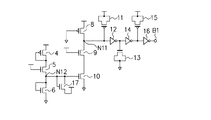
図9は、電源電圧検出回路の構成例を示す回路図である。以下、MOS電界効果トランジスタを単にトランジスタという。Pチャネルトランジスタ8は、ソースが電源電圧端子VDDに接続され、ゲートがグランド端子(基準電位端子)に接続され、ドレインがノード端子N11に接続される。Nチャネルトランジスタ9は、ソースがNチャネルトランジスタ10のドレインに接続され、ゲートが電源電圧端子VDDに接続され、ドレインがノード端子N11に接続される。Nチャネルトランジスタ10は、ソースがグランド端子に接続され、ゲートがノード端子N12に接続され、ドレインが前述の通りNチャネルトランジスタ9のソースに接続される。なお、Pチャネルトランジスタ8は、Nチャネルトランジスタ9に比べて、導通時の抵抗値が高い様に予めトランジスタの大きさを設定しておく。Nチャネルトランジスタ17は、ゲート及びソースがノード端子N12に接続され、ドレインが電源電圧端子VDDに接続される。
FIG. 9 is a circuit diagram showing a configuration example of the power supply voltage detection circuit. Hereinafter, the MOS field effect transistor is simply referred to as a transistor. The P-
Pチャネルトランジスタ4は、ソースが電源電圧端子VDDに接続され、ゲート及びドレインがNチャネルトランジスタ5のドレインに接続される。Nチャネルトランジスタ5は、ソースがノード端子N12に接続され、ゲートが電源電圧端子VDDに接続され、ドレインが前述の通りPチャネルトランジスタ4のゲート及びドレインに接続される。Nチャネルトランジスタ6は、ソースがグランド端子に接続され、ゲート及びドレインがノード端子N12に接続される。ノード端子N11は、インバータ12、インバータ14及びインバータ16を介して、電源電圧検出信号端子B1に接続される。電源電圧検出信号端子B1は、電源電圧が所定値以上であることを検出した時点でハイレベルとなる電源電圧検出信号を出力する。
The P-channel transistor 4 has a source connected to the power supply voltage terminal VDD, and a gate and a drain connected to the drain of the N-
Pチャネルトランジスタ11、Nチャネルトランジスタ13及びPチャネルトランジスタ15は、それぞれゲートがインバータ12、14及び16の各入力に接続される。Pチャネルトランジスタ11及び15は、ドレイン及びソースが電源電圧端子VDDに接続され、キャパシタとして機能する。Nチャネルトランジスタ13は、ドレイン及びソースがグランド端子に接続され、キャパシタとして機能する。キャパシタ11、13及び15は、ノード端子N11の信号の変動を遅らせるためのものである。
The gates of P-
この電源電圧検出回路において、電源電圧端子VDDの電源電圧を0Vから所定の電源電圧レベルまで上昇させた場合について動作を説明する。電源電圧が上昇した直後からトランジスタ8を通じて電源電圧端子VDD及びノード端子N11は導通状態(接続状態)となり、ノード端子N11はほぼ電源電圧に等しくなる。この時点で、トラジスタ5は、既に導通状態になっているが、ノード端子N12はトランジスタ4のドレイン及びゲートが短絡されていることにより、電源電圧に比べ電圧が少なくとも閾値電圧分下がること、さらにトランジスタ6により電流がグランド端子に流れることにより、電源電圧の電圧に従って電圧は上昇するが、トランジスタ10の閾値電圧を超えるほど上昇しない。この結果、ノード端子N11は電源電圧のままであり、電源電圧検出信号端子B1はグランドレベルのままである。
In this power supply voltage detection circuit, the operation will be described when the power supply voltage at the power supply voltage terminal VDD is raised from 0 V to a predetermined power supply voltage level. Immediately after the power supply voltage rises, the power supply voltage terminal VDD and the node terminal N11 are brought into conduction (connected state) through the
さらに、電源電圧端子VDDの電源電圧が上昇することによって、ノード端子N12の電位がさらに上がり続け、ついにトランジスタ10の閾値電圧を超える値になる。こうなると、ノード端子N11において、トランジスタ8による電源電圧端子VDDからの電圧上昇と、トランジスタ10によるグランド端子への電圧降下が同時に起こる。しかし、トランジスタ8に比べ、トランジスタ9及び10の方が低抵抗なため、最終的にノード端子N11はグランドへ向けて下がる。この結果、電源電圧検出信号端子B1は、電源電圧と等しいハイレベルを出力する。これ以降、電源電圧検出信号端子B1の電圧は、電源電圧レベルに追従する。電源電圧検出信号端子B1が電源電圧検出信号を出力した時点の電源電圧の電圧値が電源電圧検出信号の電圧値となる。
Furthermore, as the power supply voltage at the power supply voltage terminal VDD rises, the potential at the node terminal N12 continues to rise further, finally reaching a value exceeding the threshold voltage of the
電源電圧を下げていった場合については、電源電圧を上げた場合と全く逆の動作をする。すなわち、電源電圧の電圧値が所定値から0Vに下がるとすると、初期状態は、電源電圧が検出され、電源電圧検出信号端子B1の電圧値は電源電圧レベルで、トランジスタ10はオン状態である。しかし、電源電圧の電圧値が下がるとそれに伴いノード端子N12の電圧は低下し、ついに電源電圧検出電圧に達した時点でノード端子N12の電圧はトランジスタ10の閾値電圧以下になり、トランジスタ10はオフする。この結果、ノード端子N11の電圧をグランドへ向けて下げるパスが切断されるが、一方でノード端子N11には電源電圧端子VDDからの電源供給パスが存在する為、ノード端子N11は電源電圧レベルになる。この結果、電源電圧検出信号端子B1の信号は、グランドレベルになる。
When the power supply voltage is lowered, the operation is completely opposite to that when the power supply voltage is raised. That is, when the voltage value of the power supply voltage falls from the predetermined value to 0 V, the power supply voltage is detected in the initial state, the voltage value of the power supply voltage detection signal terminal B1 is the power supply voltage level, and the
前記電源電圧検出回路では、一旦電源電圧を検出すると、電源電圧検出を終了するまで電源電圧端子VDDからグランド端子までのパスは、トランジスタ4、トランジスタ5及びトランジスタ6を通じるパスと、トランジスタ8、トランジスタ9及びトランジスタ10を通じるパスとで、電流を流し続けることにより、電源電圧端子VDDの電源電圧レベルを監視している。すなわち、電力消費が常に行われていることを意味している。
In the power supply voltage detection circuit, once the power supply voltage is detected, the path from the power supply voltage terminal VDD to the ground terminal is the path through the transistor 4, the
図10は、他の電源電圧検出回路の構成例を示す回路図である。図10の回路は、図9の回路に対して、トランジスタ23,26及びインバータ37を追加したものである。Pチャネルトランジスタ26は、ソースが電源電圧端子VDDに接続され、ゲートが電源電圧検出信号端子B1に接続され、ドレインがPチャネルトランジスタ8のソースに接続される。Nチャネルトランジスタ23は、ソースがNチャネルトランジスタ6のドレイン及びゲートに接続され、ゲートがインバータ37を介して電源電圧検出信号端子B1に接続され、ドレインがノード端子N12に接続される。
FIG. 10 is a circuit diagram showing a configuration example of another power supply voltage detection circuit. The circuit of FIG. 10 is obtained by adding
図10の回路動作が図9の回路動作と異なる点を説明する。電源電圧が所定値以上になると、電源電圧検出信号端子B1の信号は、電源電圧と同じ電圧値になる。この際、トランジスタ26のゲート電圧も、電源電圧と同じになる。トランジスタ23のゲート電圧は、グランドレベルになる。そのため、トランジスタ23及びトランジスタ26は共にオフしてしまい、電源電圧端子VDD及びグランド端子間のパスが完全に切断される。
The difference between the circuit operation of FIG. 10 and the circuit operation of FIG. 9 will be described. When the power supply voltage exceeds a predetermined value, the signal at the power supply voltage detection signal terminal B1 has the same voltage value as the power supply voltage. At this time, the gate voltage of the
この結果、電源電圧検出回路は電源電圧の電圧値が所定値未満になったとしても、漏れ電流でフローティングになるノード端子N11及びノード端子N12から電荷が抜けきらない限り、電源電圧検出信号端子B1の信号は、電源電圧レベルに追従し、電源電圧検出の機能を果たせない。すなわち、電源電圧検出回路は、電源電圧が0Vから所定値に立ち上がる場合にしかその動作を行わないことを意味する。その原理を説明する。電源電圧検出回路が電圧電圧を監視するためには、電源電圧の電圧値によってノード端子N12の電圧を調整してトランジスタ10のオン/オフを制御できると共に、ノード端子N11には常に電源電圧端子VDDからの電圧供給を行い、トランジスタ10がオフした場合にはノード端子N11の電圧を電源電圧レベルに引き上げることができなければならない。しかし、電源電圧検出信号端子B1の電圧が一旦電源電圧になると、ノード端子N11は電源電圧端子VDDからの電源電圧供給パスが切断されてしまい、ローレベルでフローティングになり、ただキャパシタ11によって電源電圧の電圧値に比例したカップリング効果による電圧降下を受けるだけになる。したがって、インバータ12の入力としてのノード端子N11は、電源電圧レベルから見て常にローレベルと見えてしまい、電源電圧検出信号端子B1の電圧は、電源電圧の電圧値によらず常に電源電圧レベルに追従してしまう。これを解消するには、電源電圧が一旦0Vになった上、漏れ電流などによりフローティングノード端子N11及びN12の電荷が完全に抜けきらないといけない。さらに、ノード端子N12の電圧がトランジスタ10の閾値電圧以下になってトランジスタ10をオフさせることが必要である。なお、ノード端子N12は、トランジスタ17によりトランジスタの閾値電圧までは電圧を引き抜くパスが用意されていている。
As a result, even if the voltage value of the power supply voltage becomes less than a predetermined value, the power supply voltage detection circuit is capable of detecting the power supply voltage detection signal terminal B1 as long as the charges are not removed from the node terminal N11 and the node terminal N12 that are floating due to the leakage current. This signal follows the power supply voltage level and cannot perform the function of power supply voltage detection. That is, the power supply voltage detection circuit means that the operation is performed only when the power supply voltage rises from 0V to a predetermined value. The principle will be described. In order for the power supply voltage detection circuit to monitor the voltage voltage, the voltage of the node terminal N12 can be adjusted by the voltage value of the power supply voltage to control the on / off of the
また、下記の特許文献1には、パワーアップ期間中に特別テストモードへのエンタ等のような機能を禁止するために使用することが可能であるパワーオンリセット回路が記載されている。
上記の電源電圧検出回路では、次の問題が存在する。図9の電源電圧検出回路は、常に電源電圧の状態を把握できる、すなわち、常時電源電圧監視が可能であるが、電源電圧が所定値以上になった後も常に電源電圧端子VDD及びグランド端子間のパスが接続状態になってしまい、常に電力消費されてしまう。このことは半導体装置に求められている低消費電力と言う観点から問題である。 The above power supply voltage detection circuit has the following problems. The power supply voltage detection circuit of FIG. 9 can always grasp the state of the power supply voltage, that is, the power supply voltage can always be monitored, but always between the power supply voltage terminal VDD and the ground terminal even after the power supply voltage exceeds a predetermined value. The path becomes connected and power is always consumed. This is a problem from the viewpoint of low power consumption required for semiconductor devices.
また、図10の電源電圧検出回路は、電源電圧が0Vから初めて立ち上がった時点で、電源電圧検出信号が電源電圧端子VDD及びグランド端子間のパスを全て切断するため、電力消費は電源電圧の立ち上げ時にのみしか発生しない。しかし、一旦電源電圧が立ち上がると、この後に再び電源電圧検出を行う為には、電源電圧が一旦0Vになり、フローティングのノード端子N11及びN12の電荷が完全に抜けきらないといけないことから、例えば電源電圧が所定値より下がった状態については電源電圧の検出が不可能になる。これでは半導体装置の動作中に電源電圧が0Vに瞬間電圧低下した場合なども電源電圧検出回路はそれを検出できず、例えば電源電圧低下の保護対策を全くとれなく問題である。 In the power supply voltage detection circuit of FIG. 10, since the power supply voltage detection signal cuts all paths between the power supply voltage terminal VDD and the ground terminal when the power supply voltage rises from 0V for the first time, the power consumption is the rise of the power supply voltage. It only occurs when raising. However, once the power supply voltage rises, in order to detect the power supply voltage again, the power supply voltage once becomes 0 V, and the charges of the floating node terminals N11 and N12 must be completely removed. In a state where the power supply voltage has fallen below a predetermined value, the power supply voltage cannot be detected. In this case, even when the power supply voltage drops instantaneously to 0 V during the operation of the semiconductor device, the power supply voltage detection circuit cannot detect it, and for example, it is a problem that protection measures against power supply voltage drop cannot be taken at all.
ところで、一般的に半導体装置において電源電圧検出回路が必要な場合は、半導体装置が何らかの動作中である場合であって、電源が入っていても待機中は特に電源電圧検出回路が動作していなくとも実用上の障害はない場合がある。半導体装置は、必ずしも電源が入っている場合だけでなく、場合によっては待機中の期間の割合が大きい場合もある。 By the way, in general, when a power supply voltage detection circuit is required in a semiconductor device, the semiconductor device is in some operation, and the power supply voltage detection circuit is not particularly operated during standby even when the power is on. There may be no practical obstacles. A semiconductor device is not necessarily supplied with power, but in some cases, the ratio of a waiting period may be large.
本発明の目的は、電源電圧の立ち上がり及び立ち下がりを検出することができ、かつ電力消費を抑制することができる電源電圧検出回路を提供することである。 An object of the present invention is to provide a power supply voltage detection circuit that can detect rising and falling of a power supply voltage and can suppress power consumption.
本発明の一観点によれば、電源電圧検出信号及び外部信号に応じて電源電圧端子及び第1の端子間を接続するための第1のスイッチと、電源電圧検出信号及び外部信号に応じて基準電位端子及び第2の端子間を接続するための第2のスイッチと、前記第2の端子及び電源電圧端子間に接続される第1の抵抗と、前記第2の端子の電圧に応じて前記第1の端子及び基準電位端子間を接続するための第3のスイッチと、前記第1の端子の信号を基に前記電源電圧検出信号を出力する出力回路とを有することを特徴とする電源電圧検出回路が提供される。 According to one aspect of the present invention, a first switch for connecting a power supply voltage terminal and a first terminal according to a power supply voltage detection signal and an external signal, and a reference according to the power supply voltage detection signal and the external signal A second switch for connecting between the potential terminal and the second terminal; a first resistor connected between the second terminal and the power supply voltage terminal; and the voltage according to the voltage of the second terminal. A power supply voltage comprising: a third switch for connecting the first terminal and a reference potential terminal; and an output circuit for outputting the power supply voltage detection signal based on a signal of the first terminal. A detection circuit is provided.
外部信号を用いることにより、電源電圧の立ち上がり及び立ち下がりを検出することができ、かつ電力消費を抑制することができる。 By using an external signal, the rise and fall of the power supply voltage can be detected, and power consumption can be suppressed.
(第1の実施形態)
図1は、本発明の第1の実施形態による電源電圧検出回路の構成例を示す回路図である。この電源電圧検出回路は、半導体装置である。以下、MOS電界効果トランジスタを単にトランジスタという。Pチャネルトランジスタ46は、ソースが電源電圧端子VDDに接続され、ゲートが電源電圧検出信号端子A1に接続され、ドレインがPチャネルトランジスタ48のソースに接続される。Pチャネルトランジスタ47は、ソースが電源電圧端子VDDに接続され、ゲートが外部信号端子A2に接続され、ドレインがPチャネルトランジスタ48のソースに接続される。Pチャネルトランジスタ48は、ソースが前述の通りPチャネルトランジスタ46のドレイン及びトランジスタ47のドレインに接続され、ゲートがグランド端子(基準電位端子)に接続され、ドレインがノード端子N1に接続され、抵抗として機能する。Nチャネルトランジスタ49は、ソースがNチャネルトランジスタ50のドレインに接続され、ゲートが電源電圧端子VDDに接続され、ドレインがノード端子N1に接続され、抵抗として機能する。Nチャネルトランジスタ50は、ソースがグランド端子に接続され、ゲートがノード端子N2に接続され、ドレインが前述の通りNチャネルトランジスタ49のソースに接続される。なお、Pチャネルトランジスタ48は、Nチャネルトランジスタ49に比べて導通時の抵抗が高い様に予めトランジスタの大きさを設定しておく。Nチャネルトランジスタ57は、ゲート及びソースがノード端子N2に接続され、ドレインが電源電圧端子VDDに接続される。
(First embodiment)
FIG. 1 is a circuit diagram showing a configuration example of a power supply voltage detection circuit according to the first embodiment of the present invention. This power supply voltage detection circuit is a semiconductor device. Hereinafter, the MOS field effect transistor is simply referred to as a transistor. The
Pチャネルトランジスタ40は、ソースが電源電圧端子VDDに接続され、ゲート及びドレインがNチャネルトランジスタ41のドレインに接続される。Nチャネルトランジスタ41は、ソースがノード端子N2に接続され、ゲートが電源電圧端子VDDに接続され、ドレインが前述の通りPチャネルトランジスタ40のゲート及びドレインに接続され、抵抗として機能する。Nチャネルトランジスタ42は、ソースがNチャネルトランジスタ43のドレイン及びゲートに接続され、ゲートがインバータ58を介して電源電圧検出信号端子A1に接続され、ドレインがノード端子N2に接続される。Nチャネルトランジスタ43は、ソースがグランド端子に接続され、ゲート及びドレインが前述の通りNチャネルトランジスタ42のソースに接続される。Nチャネルトランジスタ44は、ソースがNチャネルトランジスタ43のドレイン及びゲートに接続され、ゲートがインバータ59を介して外部信号端子A2に接続され、ドレインがノード端子N2に接続される。ノード端子N1は、インバータ52、インバータ54及びインバータ56を介して、電源電圧検出信号端子A1に接続される。インバータ52、54及び56は、それぞれ入力信号を反転増幅させて出力する。その結果、電源電圧検出信号端子A1の電圧レベルは、ノード端子N1の電圧レベルを反転したレベルになる。
The
Pチャネルトランジスタ51、Nチャネルトランジスタ53及びPチャネルトランジスタ55は、それぞれゲートがインバータ52、54及び56の各入力に接続される。Pチャネルトランジスタ51及び55は、ドレイン及びソースが電源電圧端子VDDに接続され、キャパシタとして機能する。Nチャネルトランジスタ53は、ドレイン及びソースがグランド端子に接続され、キャパシタとして機能する。キャパシタ51、53及び55は、ノード端子N1の信号の変動を遅らせるためのものである。
図2は、図1の電源電圧検出回路の動作例を示すタイミングチャートであり、電源電圧端子VDDの電圧、電源電圧検出信号端子A1の電圧、外部信号端子A2の電圧、電源電圧検出回路の状態STを示す。 FIG. 2 is a timing chart showing an operation example of the power supply voltage detection circuit of FIG. 1. The voltage of the power supply voltage terminal VDD, the voltage of the power supply voltage detection signal terminal A1, the voltage of the external signal terminal A2, and the state of the power supply voltage detection circuit ST is shown.
第1の期間T1は、時刻t0〜t2の期間であり、電源電圧端子VDDの電源電圧を0Vから所定の電圧Vddまで上昇させた場合である。第1の期間T1では、外部信号端子A2にハイレベルの外部信号が入力される。初期状態の時刻t0では、回路中の全てのノードがグランドレベルである。電源電圧端子VDDの電圧が上昇した直後から、電源電圧検出信号端子A1の電圧はグランドであり、トランジスタ42及び46が導通状態になる。トランジスタ46及びトランジスタ48を通じて電源電圧端子VDD及びノード端子N1間は導通状態となる。ノード端子N1は、ほぼ電源電圧端子VDDの電圧に等しくなる。この時点で、トラジスタ41は既に導通状態になっているが、ノード端子N2はトランジスタ40のドレイン及びゲートが短絡されていることにより電源電圧端子VDDの電圧に比べ電圧が少なくとも閾値電圧分下がり、さらにトランジスタ42は導通している。トランジスタ43により電流がグランド端子に流れることにより、電源電圧端子VDDの電圧に従って、ノード端子N2の電圧は上昇するが、トランジスタ50の閾値電圧を超えるほど上昇しない。この結果、ノード端子N2は電源電圧端子VDDと同じ電圧のままであり、電源電圧検出信号端子A1はグランドレベルのままである。さらに、電源電圧端子VDDの電圧が上昇することによって、ノード端子N2の電位がさらに上がり続ける。ついに時刻t1において、電源電圧端子VDDが検出電圧V1に達すると、ノード端子N2の電位はトランジスタ50の閾値電圧を超える値になる。こうなると、ノード端子N1は、トランジスタ46及びトランジスタ48を介した電源電圧端子VDDからのパスによる電圧上昇と、トランジスタ49及びトランジスタ50を介したグランド端子へのパスによる電圧降下が同時に起こる。しかし、ノード端子N1及びグランド端子間のパスの抵抗は、電源電圧端子VDD及びノード端子N1間の抵抗よりも低いため、最終的にノード端子N1の電圧はグランドへ向けて下がる。この結果、電源電圧検出信号端子A1の電圧は、電源電圧端子VDDの電圧に追従する。また、電源電圧検出信号端子A1の電源電圧レベルは、トランジスタ46のゲートに供給される。インバータ58は、電源電圧検出信号端子A1の電源電圧レベルを反転し、グランドレベルをトランジスタ42のゲートに供給する。これにより、トランジスタ42及び46はオフし、電源電圧検出回路内の電源電圧端子VDD及びグランド端子間のパスは完全に切断され、電力消費がなされなくなる。電源電圧検出回路は、時刻t0〜t1では電源電圧検出動作状態ST1になり、時刻t1〜t2では電源電圧検出動作を行わずに電力消費なしの状態ST2になる。
The first period T1 is a period from time t0 to t2, and is a case where the power supply voltage at the power supply voltage terminal VDD is increased from 0 V to a predetermined voltage Vdd. In the first period T1, a high-level external signal is input to the external signal terminal A2. At time t0 in the initial state, all nodes in the circuit are at the ground level. Immediately after the voltage at the power supply voltage terminal VDD rises, the voltage at the power supply voltage detection signal terminal A1 is the ground, and the
次に、第2の期間T2に移る。第2の期間T2は、時刻t2〜t3の期間であり、外部信号端子A2にローレベルの外部信号が入力される。外部信号端子A2がローレベルになると、インバータ59は外部信号端子A2のローレベルを反転し、ハイレベルをトランジスタ44のゲートに出力する。これにより、トランジスタ44及び47はオンし、電源電圧検出回路内の電源電圧端子VDD及びグランド端子間のパスが再び導通状態になる。電源電圧検出回路は、第2の期間T2では電源電圧検出動作状態ST1になる。
Next, the process proceeds to the second period T2. The second period T2 is a period from time t2 to t3, and a low-level external signal is input to the external signal terminal A2. When the external signal terminal A2 becomes low level, the
次に、第3の期間T3に移る。第3の期間T3は、時刻t3以降の期間であり、電源電圧端子VDDが電圧Vddから0Vに下がる。外部信号端子A2は、ローレベルのままである。この場合、電源電圧を上げた場合と全く逆の動作をする。すなわち、時刻t3において、電源電圧端子VDDの電圧が所定値Vddから0Vに向けて下がり始めると、電源電圧検出信号端子A1は電源電圧レベルであり、トランジスタ50はオン状態である。しかし、電源電圧端子VDDの電圧が下がると、それに伴いノード端子N2の電圧は低下する。ついに、時刻t4において、電源電圧端子VDDの電圧が検出電圧V1に低下した時点で、ノード端子N2の電圧はトランジスタ50の閾値電圧以下になり、トランジスタ50はオフする。この結果、ノード端子N1の電圧をグランドへ下げるパスが切断される。一方で、ノード端子N1にはトランジスタ47及びトランジスタ48を通じて電源電圧端子VDDからの電源電圧供給パスが存在するため、ノード端子N1は電源電圧レベルになる。この結果、電源電圧検出信号端子A1はグランドレベルになる。電源電圧検出回路は、第3の期間T3では第2の期間T2と同じく電源電圧検出動作状態ST1である。
Next, the process proceeds to the third period T3. The third period T3 is a period after time t3, and the power supply voltage terminal VDD drops from the voltage Vdd to 0V. The external signal terminal A2 remains at a low level. In this case, the operation is completely opposite to that when the power supply voltage is increased. That is, when the voltage at the power supply voltage terminal VDD starts to decrease from the predetermined value Vdd toward 0 V at time t3, the power supply voltage detection signal terminal A1 is at the power supply voltage level, and the
以上のように、トランジスタ42、44、46、47及び50は、スイッチとして機能する。スイッチ46及び47は、電源電圧端子VDD及びノード端子N1間に並列に接続され、電源電圧検出信号端子A1及び外部信号端子A2の信号に応じて電源電圧端子VDD及びノード端子N1間を接続するためのスイッチである。スイッチ46は、電源電圧検出信号端子A1の信号に応じて電源電圧端子VDD及びノード端子N1間を接続する。スイッチ47は、外部信号端子A2の信号に応じて電源電圧端子VDD及びノード端子N1間を接続する。スイッチ46及び47は、同一の抵抗48を介してノード端子N1に接続される。これにより、時刻t1の電源電圧立ち上がり時の検出電圧V1と時刻t4の電源電圧立ち下がり時の検出電圧V1とが同じになる。
As described above, the
スイッチ42及び44は、グランド端子及びノード端子N2間に並列に接続され、電源電圧検出信号端子A1及び外部信号端子A2の信号に応じてグランド端子(基準電位端子)及びノード端子N2間を接続するためのスイッチである。スイッチ42は、電源電圧検出信号端子A1の信号に応じてグランド端子及びノード端子N2間を接続する。スイッチ44は、外部信号端子A2の信号に応じてグランド端子及びノード端子N2間を接続する。
The
抵抗41は、ノード端子N2及び電源電圧端子VDD間に接続される。スイッチ50は、ノード端子N2の電圧に応じてノード端子N1及びグランド端子間を接続するためのスイッチである。インバータ52、54、56及びキャパシタ51、53、55は、ノード端子N1の信号を基に電源電圧検出信号端子A2に電源電圧検出信号を出力する出力回路である。
The
電源電圧検出信号端子A1の信号は、電源電圧が所定値V1以上であるか否かを示す信号である。スイッチ42及び46は、電源電圧検出信号端子A1の信号がローレベル(電源電圧が所定値V1未満)であるときには接続する。また、スイッチ42及び46は、電源電圧検出信号端子A1の信号がハイレベル(電源電圧が所定値V1以上)である場合において、外部信号端子A2の信号がローレベル(接続指示)であれば接続し、ハイレベルであれば(接続指示がなければ)切断する。
The signal at the power supply voltage detection signal terminal A1 is a signal indicating whether the power supply voltage is equal to or higher than a predetermined value V1. The
本実施形態によれば、電源立ち上げ時の初期状態は図2の時刻t0〜t1にあたり、電源電圧の検出動作が行われる。時刻t1〜t2では、電源電圧の検出動作を行わないが、電源電圧端子VDD及びグランド端子間のパスが切断されているため、電力消費は殆ど無くなる。時刻t2以降では、外部信号により電源電圧端子VDD及びグランド端子間のパスを再び導通化させることで、電源電圧の検出を再び行うことができる。また、時刻t2のタイミングは、外部信号により任意に変更ができるため、電源電圧の検出が必要な期間を外部信号により制御し、その上電源電圧の検出が必要でない期間は電力の消費を抑えることが可能になる。例えば、外部信号は、他の機能ブロック(例えば半導体メモリ)のスタンバイ/アクティブ信号であり、ハイレベルがスタンバイ信号を意味し、ローレベルがアクティブ信号を意味する。 According to the present embodiment, the initial state when the power is turned on corresponds to the time t0 to t1 in FIG. 2, and the power supply voltage detection operation is performed. At time t1 to t2, the power supply voltage detection operation is not performed, but the power consumption is almost eliminated because the path between the power supply voltage terminal VDD and the ground terminal is disconnected. After time t2, the power supply voltage can be detected again by making the path between the power supply voltage terminal VDD and the ground terminal conductive again by an external signal. In addition, since the timing at time t2 can be arbitrarily changed by an external signal, the period in which the power supply voltage needs to be detected is controlled by the external signal, and the power consumption is suppressed in the period in which the power supply voltage is not required to be detected. Is possible. For example, the external signal is a standby / active signal of another functional block (for example, a semiconductor memory), a high level means a standby signal, and a low level means an active signal.
(第2の実施形態)
図3は、本発明の第2の実施形態による電源電圧検出回路の構成例を示す回路図である。以下、本実施形態が第1の実施形態と異なる点を説明する。本実施形態は、第1の実施形態(図1)のトランジスタ47、トランジスタ44及びインバータ59を取り除き、トランジスタ46のゲート及びインバータ58の入力を次のように変更した回路である。インバータ60は、電源電圧検出信号端子A1の信号を反転して出力する。否定論理和(NOR)回路61は、インバータ60の出力信号と外部信号端子A2の信号との否定論理和信号を出力する。インバータ58は、NOR回路61の出力信号を反転して出力する。トランジスタ46のゲートには、NOR回路61の出力信号が入力される。トランジスタ42のゲートには、インバータ58の出力信号が入力される。
(Second Embodiment)
FIG. 3 is a circuit diagram showing a configuration example of a power supply voltage detection circuit according to the second embodiment of the present invention. Hereinafter, the points of the present embodiment different from the first embodiment will be described. In this embodiment, the
以上のように、トランジスタ46は、ゲートに電源電圧検出信号端子A1及び外部信号端子A2の信号を論理演算した論理演算信号が入力されるスイッチングトランジスタである。トランジスタ42は、ゲートに前記論理演算信号の反転信号が入力されるスイッチングトランジスタである。
As described above, the
本実施形態の電源電圧検出回路の動作は、第1の実施形態の動作と同じである。両者の相違点は、インバータ60及びNOR回路61を含む論理回路により、電源電圧端子VDD及びグランド端子間のパスのトランジスタ42及び46の接続/切断を制御することである。なお、第2の実施形態で示したトランジスタ46のゲート電圧及びトランジスタ42のゲート電圧を制御する論理回路は、単なる一例を示したものであり、本論理と結果的に同一であれば任意の論理回路で構成しても良いのは当然である。
The operation of the power supply voltage detection circuit of this embodiment is the same as that of the first embodiment. The difference between the two is that the logic circuit including the
(第3の実施形態)
図4は、本発明の第3の実施形態による電源電圧検出回路の構成例を示す回路図である。以下、本実施形態が第1の実施形態と異なる点を説明する。本実施形態は、第1の実施形態(図1)のトランジスタ47を取り払った上で、トランジスタ62及び63を追加したものである。Pチャネルトランジスタ62は、ソースが電源電圧端子VDDに接続され、ゲートが外部信号端子A2に接続され、ドレインがPチャネルトランジスタ63のソースに接続され、スイッチとして機能する。Pチャネルトランジスタ63は、ソースがPチャネルトランジスタ62のドレインに接続され、ゲートがグランド端子に接続され、ドレインがノード端子N1に接続され、抵抗として機能する。
(Third embodiment)
FIG. 4 is a circuit diagram showing a configuration example of a power supply voltage detection circuit according to the third embodiment of the present invention. Hereinafter, the points of the present embodiment different from the first embodiment will be described. In this embodiment, the
本実施形態では、電源電圧端子VDDからノード端子N1までのパスは、トランジスタ46及びトランジスタ48を通るパスと、トランジスタ62及びトランジスタ63を通るパスが並列して存在する。トランジスタ48の大きさを調整してトランジスタ48の抵抗値を制御することにより、電源電圧立ち上がり時の検出電圧V1を調整することができる。また、トランジスタ63の大きさを調整してトランジスタ63の抵抗値を制御することにより、電源電圧立ち下がり時の検出電圧V2を調整することができる。
In the present embodiment, the path from the power supply voltage terminal VDD to the node terminal N1 includes a path passing through the
図5は、図4の電源電圧検出回路の動作例を示すタイミングチャートである。本実施形態が第1の実施形態(図2)と異なる点を説明する。第1の期間T1は、電源電圧の立ち上がりを検出する期間であり、第1の実施形態と同一の動作をする。時刻t1において、電源電圧端子VDDの電圧が検出電圧V1まで立ち上がると、電源電圧検出信号端子A1はハイレベル(電源電圧レベル)を出力する。この時、トランジスタ46及び48を介して電源電圧端子VDD及びノード端子N1間のパスが導通するので、トランジスタ48の抵抗値に応じて検出電圧V1が決まる。第2の期間T2は、外部信号端子A2の信号がローレベル(グランドレベル)になると、トランジスタ62が導通し、電源電圧端子VDD及びグランド端子間のパスがトランジスタ62及び63を介して通じるようになる。第3の期間T3では、電源電圧端子VDDは所定電圧Vddから0Vに下がる。時刻t4において、電源電圧端子VDDの電圧が検出電圧V2まで立ち下がると、電源電圧検出信号端子A1はローレベルを出力する。この際に、トランジスタ50が切断された後、ノード端子N1を電源電圧レベルに引き上げるパスは、第1の期間T1での電源電圧立ち上がり時のパスとは異なり、トランジスタ62及び63を介した電源電圧端子VDD及びノード端子N1間のパスになる。そのため、トランジスタ63の抵抗値に応じて検出電圧V2が決まる。トランジスタ48及び63の抵抗値により、電源電圧の立ち上がり時の検出電圧V1と立ち下がり時の検出電圧V2とを変えることが可能になる。
FIG. 5 is a timing chart showing an operation example of the power supply voltage detection circuit of FIG. Differences of this embodiment from the first embodiment (FIG. 2) will be described. The first period T1 is a period during which the rising of the power supply voltage is detected, and performs the same operation as in the first embodiment. When the voltage at the power supply voltage terminal VDD rises to the detection voltage V1 at time t1, the power supply voltage detection signal terminal A1 outputs a high level (power supply voltage level). At this time, since the path between the power supply voltage terminal VDD and the node terminal N1 is conducted through the
以上のように、スイッチ46及び62は、電源電圧端子VDD及びノード端子N1間に並列に接続され、異なる抵抗48及び63を介してノード端子N1に接続される。スイッチ46は、電源電圧検出信号端子A1の信号に応じて電源電圧端子VDD及びノード端子N1間を接続する。スイッチ62は、外部信号端子A2の信号に応じて電源電圧端子VDD及びノード端子N1間を接続する。
As described above, the
(第4の実施形態)
図6は、本発明の第4の実施形態による電源電圧検出回路の構成例を示す回路図である。以下、本実施形態が第1の実施形態と異なる点を説明する。本実施形態は、第1の実施形態(図1)のトランジスタ44、47及びインバータ59を取り除き、スイッチ回路64及び65を追加したものである。
(Fourth embodiment)
FIG. 6 is a circuit diagram showing a configuration example of a power supply voltage detection circuit according to the fourth embodiment of the present invention. Hereinafter, the points of the present embodiment different from the first embodiment will be described. In the present embodiment, the
スイッチ回路64は、電源電圧端子VDD及びトランジスタ48のソース間に並列に接続された複数のPチャネルトランジスタ71を有する。複数のトランジスタ71のゲートには、それぞれ外部信号端子A21〜A23等の信号が入力される。
The
スイッチ回路65は、ノード端子N2及びトランジスタ43のドレイン間に並列に接続された複数のNチャネルトランジスタ72を有する。複数のトランジスタ72のゲートには、それぞれインバータ73を介して外部信号端子A21〜A23等が接続され、外部信号端子A21〜A23等の信号の反転信号が入力される。
The
スイッチ回路64は、第1の実施形態のトランジスタ44に相当するトランジスタ71を並列に2列以上接続した回路である。スイッチ回路65は、第1の実施形態のトランジスタ47に相当するトランジスタ72を並列に2列以上接続した回路である。スイッチ回路64及び65を構成するトランジスタ71及び72の各々のゲートには、各々別々の外部信号端子A21〜A23等が1対1で接続されている。
The
スイッチ回路64及び65は、複数の外部信号端子A21〜A23等の信号のうちの少なくとも1つがローレベル(接続指示)であれば接続し、1つもローレベル(接続指示)がなければ切断する。
The
すなわち、電源電圧端子VDD及びノード端子N1間のパスのスイッチ46,71は、電源電圧検出信号端子A1がハイレベル(電源電圧が所定値V1以上)である場合において、複数の外部信号端子A21〜A23等の信号のうちの少なくとも1つがローレベル(接続指示)であれば電源電圧端子VDD及びノード端子N1間のパスを接続し、1つもローレベル(接続指示)がなければ電源電圧端子VDD及びノード端子N1間のパスを切断する。
That is, the
同様に、ノード端子N2及びグランド端子間のパスのスイッチ42,72は、電源電圧検出信号端子A1がハイレベル(電源電圧が所定値V1以上)である場合において、複数の外部信号端子A21〜A23等の信号のうちの少なくとも1つがローレベル(接続指示)であればグランド端子及びノード端子N2間のパスを接続し、1つもローレベル(接続指示)がなければグランド端子及びノード端子N2間のパスを切断する。
Similarly, the
複数の外部信号端子A21〜A23等の信号のうち少なくとも1つがローレベルになると、トランジスタ71及び72がオンし、図1のトランジスタ44及び47がオンしたときと同じ動作を行う。すなわち、図2の時刻t2における動作を行い、それ以降は電源電圧検出が可能になる。
When at least one of the signals from the plurality of external signal terminals A21 to A23 becomes low level, the
(第5の実施形態)
図7は、本発明の第5の実施形態による電源電圧検出回路の構成例を示す回路図である。以下、本実施形態が第1の実施形態と異なる点を説明する。本実施形態は、第1の実施形態(図1)のトランジスタ44、47及びインバータ59を取り除き、スイッチ回路66及び67を追加したものである。
(Fifth embodiment)
FIG. 7 is a circuit diagram showing a configuration example of a power supply voltage detection circuit according to the fifth embodiment of the present invention. Hereinafter, the points of the present embodiment different from the first embodiment will be described. In this embodiment, the
スイッチ回路66は、電源電圧端子VDD及びトランジスタ48のソース間に直列に接続された複数のPチャネルトランジスタ74を有する。複数のトランジスタ74のゲートには、それぞれ外部信号端子A31〜A33等の信号が入力される。
The switch circuit 66 includes a plurality of P-
スイッチ回路67は、ノード端子N2及びトランジスタ43のドレイン間に直列に接続された複数のNチャネルトランジスタ75を有する。複数のトランジスタ75のゲートには、それぞれインバータ76を介して外部信号端子A31〜A33等が接続され、外部信号端子A31〜A33等の信号の反転信号が入力される。
The
スイッチ回路66は、第1の実施形態のトランジスタ44に相当するトランジスタ74を直列に2段以上接続した回路である。スイッチ回路67は、第1の実施形態のトランジスタ47に相当するトランジスタ75を直列に2段以上接続した回路である。スイッチ回路66及び67を構成するトランジスタ74及び75の各々のゲートには、各々別々の外部信号端子A31〜A33等が1対1で接続されている。
The switch circuit 66 is a circuit in which two or more stages of
スイッチ回路66内の全トランジスタ74の合計サイズ(抵抗値)は、トランジスタ46のサイズ(抵抗値)と同じになるように調整する。また、スイッチ回路67内の全トランジスタ75の合計サイズ(抵抗値)は、トランジスタ42のサイズ(抵抗値)と同じになるように調整する。
The total size (resistance value) of all the
スイッチ回路66及び67は、複数の外部信号端子A31〜A33等の信号のすべてがローレベル(接続指示)であれば接続し、少なくとも1つがローレベル(接続指示)でなければ切断する。
The
すなわち、スイッチ46及び66は、電源電圧検出信号端子A1の信号がハイレベル(電源電圧が所定値V1以上)である場合において、複数の外部信号端子A31〜A33等の信号のすべてがローレベル(接続指示)であれば電源電圧端子VDD及びノード端子N1間のパスを接続し、少なくとも1つがローレベル(接続指示)でなければ電源電圧端子VDD及びノード端子N1間のパスを切断する。
That is, in the
同様に、スイッチ42及び67は、電源電圧検出信号端子A1の信号がハイレベル(電源電圧が所定値V1以上)である場合において、複数の外部信号端子A31〜A33等の信号のすべてがローレベル(接続指示)であればグランド端子及びノード端子N2間のパスを接続し、少なくとも1つがローレベル(接続指示)でなければグランド端子及びノード端子N2間のパスを切断する。 Similarly, when the signal at the power supply voltage detection signal terminal A1 is at a high level (the power supply voltage is equal to or higher than the predetermined value V1), all of the signals from the plurality of external signal terminals A31 to A33 are at a low level. If (connection instruction), the path between the ground terminal and the node terminal N2 is connected, and if at least one of them is at a low level (connection instruction), the path between the ground terminal and the node terminal N2 is disconnected.
複数の外部信号端子A31〜A33等の信号のすべてがローレベルになると、スイッチ66及び67がオンし、図1のトランジスタ44及び47がオンしたときと同じ動作を行う。すなわち、図2の時刻t2における動作を行い、それ以降は電源電圧検出が可能になる。
When all of the signals from the plurality of external signal terminals A31 to A33 are at a low level, the
(第6の実施形態)
図8は、本発明の第6の実施形態による電源電圧検出回路の構成例を示す回路図である。以下、本実施形態が第1の実施形態と異なる点を説明する。本実施形態は、第4の実施形態及び第5の実施形態を組み合わせた実施形態である。本実施形態は、第1の実施形態(図1)のトランジスタ44、47及びインバータ59を取り除き、スイッチ回路68及び69を追加したものである。
(Sixth embodiment)
FIG. 8 is a circuit diagram showing a configuration example of a power supply voltage detection circuit according to the sixth embodiment of the present invention. Hereinafter, the points of the present embodiment different from the first embodiment will be described. This embodiment is an embodiment in which the fourth embodiment and the fifth embodiment are combined. In the present embodiment, the
外部信号は、複数のグループの外部信号に分類される。外部信号端子A41〜A43等は、第1のグループを構成する外部信号の端子である。外部信号端子A51〜A52等は、第2のグループを構成する外部信号の端子である。 External signals are classified into a plurality of groups of external signals. The external signal terminals A41 to A43 and the like are external signal terminals that constitute the first group. The external signal terminals A51 to A52 and the like are external signal terminals constituting the second group.
スイッチ回路68は、スイッチ46と並列に接続され、互いに並列に接続される複数のPチャネルトランジスタ77の直列接続を有する。第1の直列接続を構成するトランジスタ78は、それぞれゲートに第1のグループの複数の外部信号端子A41〜A43等の信号が入力される。第2の直列接続を構成するトランジスタ78は、それぞれゲートに第2のグループの複数の外部信号端子A51〜A52等の信号が入力される。
スイッチ回路69は、スイッチ42と並列に接続され、互いに並列に接続される複数のNチャネルトランジスタ79の直列接続を有する。第1の直列接続を構成するトランジスタ79は、それぞれゲートにインバータ80を介して第1のグループの複数の外部信号端子A41〜A43等が接続され、外部信号端子A41〜A43等の信号の反転信号が入力される。第2の直列接続を構成するトランジスタ79は、それぞれゲートにインバータ80を介して第2のグループの複数の外部信号端子A51〜A52等が接続され、外部信号端子A51〜A52等の信号の反転信号が入力される。
スイッチ回路68及び69は、第1又は第2のグループ内の複数の外部信号のすべてがローレベル(接続指示)であれば接続し、それ以外であれば切断する。例えば、第1のグループ内のすべての外部信号A41〜A43等がローレベルであれば、スイッチ回路68及び69は接続する。その条件を満たさなくても、第2のグループ内のすべての外部信号A51〜A52等がローレベルであれば、スイッチ回路68及び69は接続する。
The
すなわち、スイッチ46及び68は、電源電圧検出信号端子A1の信号がハイレベル(電源電圧が所定値V1以上)である場合において、第1又は第2のグループ内の複数の外部信号のすべてがローレベル(接続指示)であれば電源電圧端子VDD及びノード端子N1間のパスを接続し、それ以外であれば電源電圧端子VDD及びノード端子N1間のパスを切断する。
That is, when the signal at the power supply voltage detection signal terminal A1 is at a high level (the power supply voltage is equal to or higher than the predetermined value V1), the
同様に、スイッチ42及び69は、電源電圧検出信号端子A1の信号がハイレベル(電源電圧が所定値V1以上)である場合において、第1又は第2のグループ内の複数の外部信号のすべてがローレベル(接続指示)であればグランド端子及びノード端子N2間のパスを接続し、それ以外であればグランド端子及びノード端子N2間のパスを切断する。
Similarly, when the signal at the power supply voltage detection signal terminal A1 is at a high level (the power supply voltage is equal to or higher than the predetermined value V1), the
本実施形態は、外部信号の必要に応じた組み合わせ信号がローレベルで活性化された場合のみ電源電圧検出を行うことが可能になる。 In the present embodiment, the power supply voltage can be detected only when the combination signal according to the necessity of the external signal is activated at the low level.
なお、第1〜第6の実施形態では、外部信号がローレベルになると電源電圧検出回路が活性化する場合について説明したが、これが所定のハイレベルに相当するレベルで活性化する場合においても各々の実施形態での外部信号の入力論理を反転することで適用可能である。 In the first to sixth embodiments, the case where the power supply voltage detection circuit is activated when the external signal becomes the low level has been described, but each case where the power supply voltage detection circuit is activated at a level corresponding to a predetermined high level. In this embodiment, the present invention can be applied by inverting the input logic of the external signal.
以上のように、半導体回路の動作信号である外部信号を電源電圧検出回路に入力することにより、半導体回路の特定の動作信号が活性化されている間は、電源電圧検出回路を常時電源監視の状態に置き、動作中の異常電圧を感知させることができる。そして、半導体回路の動作信号が非活性化されている状態の時は電源電圧検出回路の電源電圧端子VDD及びグランド端子間のパスを全て切断することで、電力消費を殆ど無くすことができる。すなわち、特定の動作信号の活性化/非活性化の制御により、任意に電源電圧検出回路での監視が必要な期間を設定し、さらに電源監視が不要な期間においては電力消費を殆ど無くすことが可能になる。電源電圧の立ち上がり及び立ち下がりを検出することができ、かつ電力消費を抑制することができる。 As described above, by inputting an external signal, which is an operation signal of the semiconductor circuit, to the power supply voltage detection circuit, the power supply voltage detection circuit is constantly monitored while the specific operation signal of the semiconductor circuit is activated. An abnormal voltage during operation can be sensed by placing it in a state. When the operation signal of the semiconductor circuit is in an inactive state, the power consumption can be almost eliminated by disconnecting all the paths between the power supply voltage terminal VDD and the ground terminal of the power supply voltage detection circuit. That is, by controlling activation / deactivation of a specific operation signal, a period in which monitoring by the power supply voltage detection circuit is arbitrarily set can be arbitrarily set, and power consumption can be almost eliminated in a period in which power supply monitoring is unnecessary. It becomes possible. The rise and fall of the power supply voltage can be detected, and power consumption can be suppressed.
なお、上記実施形態は、何れも本発明を実施するにあたっての具体化の例を示したものに過ぎず、これらによって本発明の技術的範囲が限定的に解釈されてはならないものである。すなわち、本発明はその技術思想、またはその主要な特徴から逸脱することなく、様々な形で実施することができる。 The above-described embodiments are merely examples of implementation in carrying out the present invention, and the technical scope of the present invention should not be construed in a limited manner. That is, the present invention can be implemented in various forms without departing from the technical idea or the main features thereof.
本発明の実施形態は、例えば以下のように種々の適用が可能である。 The embodiment of the present invention can be applied in various ways as follows, for example.
(付記1)
電源電圧検出信号及び外部信号に応じて電源電圧端子及び第1の端子間を接続するための第1のスイッチと、
電源電圧検出信号及び外部信号に応じて基準電位端子及び第2の端子間を接続するための第2のスイッチと、
前記第2の端子及び電源電圧端子間に接続される第1の抵抗と、
前記第2の端子の電圧に応じて前記第1の端子及び基準電位端子間を接続するための第3のスイッチと、
前記第1の端子の信号を基に前記電源電圧検出信号を出力する出力回路と
を有することを特徴とする電源電圧検出回路。
(付記2)
前記第1の端子及び基準電位端子間の抵抗値は、前記第1の端子及び電源電圧端子間の抵抗値よりも小さいことを特徴とする付記1記載の電源電圧検出回路。
(付記3)
前記電源電圧検出信号は、電源電圧が所定値以上であるか否かを示す信号であり、
前記第1及び第2のスイッチは、電源電圧が所定値未満であるときには接続することを特徴とする付記1記載の電源電圧検出回路。
(付記4)
前記第1及び第2のスイッチは、電源電圧が所定値以上である場合において、外部信号の接続指示があれば接続し、接続指示がなければ切断することを特徴とする付記3記載の電源電圧検出回路。
(付記5)
前記第1のスイッチは、電源電圧端子及び前記第1の端子間に並列に接続される第4及び第5のスイッチを有し、
前記第4のスイッチは、前記電源電圧検出信号に応じて電源電圧端子及び前記第1の端子間を接続し、
前記第5のスイッチは、前記外部信号に応じて電源電圧端子及び前記第1の端子間を接続し、
前記第2のスイッチは、基準電位端子及び前記第2の端子間に並列に接続される第6及び第7のスイッチを有し、
前記第6のスイッチは、前記電源電圧検出信号に応じて基準電位端子及び前記第2の端子間を接続し、
前記第7のスイッチは、前記外部信号に応じて基準電位端子及び前記第2の端子間を接続することを特徴とする付記1記載の電源電圧検出回路。
(付記6)
前記第4及び第5のスイッチは、同一の抵抗を介して前記第1の端子に接続されることを特徴とする付記5記載の電源電圧検出回路。
(付記7)
前記第4及び第5のスイッチは、異なる抵抗を介して前記第1の端子に接続されることを特徴とする付記5記載の電源電圧検出回路。
(付記8)
前記第4のスイッチは、ゲートに前記電源電圧検出信号が入力される第1のPチャネル電界効果トランジスタであり、
前記第5のスイッチは、ゲートに前記外部信号が入力される第2のPチャネル電界効果トランジスタであり、
前記第6のスイッチは、ゲートに前記電源電圧検出信号の反転信号が入力される第1のNチャネル電界効果トランジスタであり、
前記第7のスイッチは、ゲートに前記外部信号の反転信号が入力される第2のNチャネル電界効果トランジスタであることを特徴とする付記5記載の電源電圧検出回路。
(付記9)
前記第1及び第2のPチャネル電界効果トランジスタは、同一の抵抗を介して前記第1の端子に接続されることを特徴とする付記8記載の電源電圧検出回路。
(付記10)
前記第1及び第2のPチャネル電界効果トランジスタは、異なる抵抗を介して前記第1の端子に接続されることを特徴とする付記8記載の電源電圧検出回路。
(付記11)
前記第1のスイッチは、ゲートに前記電源電圧検出信号及び前記外部信号を論理演算した論理演算信号が入力される第1のPチャネル電界効果トランジスタであり、
前記第2のスイッチは、ゲートに前記論理演算信号の反転信号が入力される第1のNチャネル電界効果トランジスタであることを特徴とする付記1記載の電源電圧検出回路。
(付記12)
前記外部信号は複数あり、
前記第1及び第2のスイッチは、電源電圧が所定値以上である場合において、前記複数の外部信号のうちの少なくとも1つが接続指示であれば接続し、1つも接続指示がなければ切断することを特徴とする付記4記載の電源電圧検出回路。
(付記13)
前記第1のスイッチは、電源電圧端子及び前記第1の端子間に並列に接続される第4及び第5のスイッチを有し、
前記第4のスイッチは、前記電源電圧検出信号に応じて電源電圧端子及び前記第1の端子間を接続し、
前記第5のスイッチは、前記複数の外部信号に応じて電源電圧端子及び前記第1の端子間を接続し、
前記第2のスイッチは、基準電位端子及び前記第2の端子間に並列に接続される第6及び第7のスイッチを有し、
前記第6のスイッチは、前記電源電圧検出信号に応じて基準電位端子及び前記第2の端子間を接続し、
前記第7のスイッチは、前記複数の外部信号に応じて基準電位端子及び前記第2の端子間を接続することを特徴とする付記12記載の電源電圧検出回路。
(付記14)
前記第4のスイッチは、ゲートに前記電源電圧検出信号が入力されるPチャネル電界効果トランジスタであり、
前記第5のスイッチは、それぞれゲートに前記複数の外部信号が入力され、並列に接続される複数のPチャネル電界効果トランジスタを有し、
前記第6のスイッチは、ゲートに前記電源電圧検出信号の反転信号が入力されるNチャネル電界効果トランジスタであり、
前記第7のスイッチは、それぞれゲートに前記複数の外部信号の反転信号が入力され、並列に接続される複数のNチャネル電界効果トランジスタを有することを特徴とする付記13記載の電源電圧検出回路。
(付記15)
前記外部信号は複数あり、
前記第1及び第2のスイッチは、電源電圧が所定値以上である場合において、前記複数の外部信号のすべてが接続指示であれば接続し、少なくとも1つが接続指示でなければ切断することを特徴とする付記4記載の電源電圧検出回路。
(付記16)
前記第1のスイッチは、電源電圧端子及び前記第1の端子間に並列に接続される第4及び第5のスイッチを有し、
前記第4のスイッチは、前記電源電圧検出信号に応じて電源電圧端子及び前記第1の端子間を接続し、
前記第5のスイッチは、前記複数の外部信号に応じて電源電圧端子及び前記第1の端子間を接続し、
前記第2のスイッチは、基準電位端子及び前記第2の端子間に並列に接続される第6及び第7のスイッチを有し、
前記第6のスイッチは、前記電源電圧検出信号に応じて基準電位端子及び前記第2の端子間を接続し、
前記第7のスイッチは、前記複数の外部信号に応じて基準電位端子及び前記第2の端子間を接続することを特徴とする付記15記載の電源電圧検出回路。
(付記17)
前記第4のスイッチは、ゲートに前記電源電圧検出信号が入力されるPチャネル電界効果トランジスタであり、
前記第5のスイッチは、それぞれゲートに前記複数の外部信号が入力され、直列に接続される複数のPチャネル電界効果トランジスタを有し、
前記第6のスイッチは、ゲートに前記電源電圧検出信号の反転信号が入力されるNチャネル電界効果トランジスタであり、
前記第7のスイッチは、それぞれゲートに前記複数の外部信号の反転信号が入力され、直列に接続される複数のNチャネル電界効果トランジスタを有することを特徴とする付記16記載の電源電圧検出回路。
(付記18)
前記外部信号は、第1のグループを構成する複数の外部信号と第2のグループを構成する複数の外部信号を有し、
前記第1及び第2のスイッチは、電源電圧が所定値以上である場合において、前記第1又は第2のグループ内の複数の外部信号のすべてが接続指示であれば接続し、それ以外であれば切断することを特徴とする付記4記載の電源電圧検出回路。
(付記19)
前記第1のスイッチは、電源電圧端子及び前記第1の端子間に並列に接続される第4及び第5のスイッチを有し、
前記第4のスイッチは、前記電源電圧検出信号に応じて電源電圧端子及び前記第1の端子間を接続し、
前記第5のスイッチは、前記第1及び第2のグループの外部信号に応じて電源電圧端子及び前記第1の端子間を接続し、
前記第2のスイッチは、基準電位端子及び前記第2の端子間に並列に接続される第6及び第7のスイッチを有し、
前記第6のスイッチは、前記電源電圧検出信号に応じて基準電位端子及び前記第2の端子間を接続し、
前記第7のスイッチは、前記第1及び第2のグループの外部信号に応じて基準電位端子及び前記第2の端子間を接続することを特徴とする付記18記載の電源電圧検出回路。
(付記20)
前記第4のスイッチは、ゲートに前記電源電圧検出信号が入力されるPチャネル電界効果トランジスタであり、
前記第5のスイッチは、互いに並列に接続される第8及び第9のスイッチを有し、
前記第8のスイッチは、それぞれゲートに前記第1のグループの複数の外部信号が入力され、直列に接続される複数のPチャネル電界効果トランジスタを有し、
前記第9のスイッチは、それぞれゲートに前記第2のグループの複数の外部信号が入力され、直列に接続される複数のPチャネル電界効果トランジスタを有し、
前記第6のスイッチは、ゲートに前記電源電圧検出信号の反転信号が入力されるNチャネル電界効果トランジスタであり、
前記第7のスイッチは、互いに並列に接続される第10及び第11のスイッチを有し、
前記第10のスイッチは、それぞれゲートに前記第1のグループの複数の外部信号の反転信号が入力され、直列に接続される複数のNチャネル電界効果トランジスタを有し、
前記第11のスイッチは、それぞれゲートに前記第2のグループの複数の外部信号の反転信号が入力され、直列に接続される複数のNチャネル電界効果トランジスタを有することを特徴とする付記19記載の電源電圧検出回路。
(Appendix 1)
A first switch for connecting the power supply voltage terminal and the first terminal according to the power supply voltage detection signal and the external signal;
A second switch for connecting the reference potential terminal and the second terminal according to the power supply voltage detection signal and the external signal;
A first resistor connected between the second terminal and a power supply voltage terminal;
A third switch for connecting the first terminal and a reference potential terminal according to the voltage of the second terminal;
An output circuit that outputs the power supply voltage detection signal based on a signal of the first terminal.
(Appendix 2)
The power supply voltage detection circuit according to
(Appendix 3)
The power supply voltage detection signal is a signal indicating whether the power supply voltage is a predetermined value or more,
The power supply voltage detection circuit according to
(Appendix 4)
The power supply voltage according to appendix 3, wherein when the power supply voltage is equal to or higher than a predetermined value, the first and second switches are connected if there is an external signal connection instruction and disconnected if there is no connection instruction. Detection circuit.
(Appendix 5)
The first switch has fourth and fifth switches connected in parallel between a power supply voltage terminal and the first terminal,
The fourth switch connects between a power supply voltage terminal and the first terminal according to the power supply voltage detection signal,
The fifth switch connects a power supply voltage terminal and the first terminal according to the external signal,
The second switch includes sixth and seventh switches connected in parallel between a reference potential terminal and the second terminal,
The sixth switch connects a reference potential terminal and the second terminal according to the power supply voltage detection signal,
The power supply voltage detection circuit according to
(Appendix 6)
The power supply voltage detection circuit according to
(Appendix 7)
The power supply voltage detection circuit according to
(Appendix 8)
The fourth switch is a first P-channel field effect transistor in which the power supply voltage detection signal is input to a gate,
The fifth switch is a second P-channel field effect transistor in which the external signal is input to a gate;
The sixth switch is a first N-channel field effect transistor in which an inverted signal of the power supply voltage detection signal is input to a gate,
The power supply voltage detection circuit according to
(Appendix 9)
9. The power supply voltage detection circuit according to
(Appendix 10)
9. The power supply voltage detection circuit according to
(Appendix 11)
The first switch is a first P-channel field effect transistor having a gate that receives a logical operation signal obtained by performing a logical operation on the power supply voltage detection signal and the external signal
2. The power supply voltage detection circuit according to
(Appendix 12)
There are a plurality of external signals,
The first and second switches are connected if at least one of the plurality of external signals is a connection instruction when the power supply voltage is equal to or higher than a predetermined value, and disconnected if no connection instruction is given. The power supply voltage detection circuit according to appendix 4, characterized by:
(Appendix 13)
The first switch has fourth and fifth switches connected in parallel between a power supply voltage terminal and the first terminal,
The fourth switch connects between a power supply voltage terminal and the first terminal according to the power supply voltage detection signal,
The fifth switch connects a power supply voltage terminal and the first terminal according to the plurality of external signals,
The second switch includes sixth and seventh switches connected in parallel between a reference potential terminal and the second terminal,
The sixth switch connects a reference potential terminal and the second terminal according to the power supply voltage detection signal,
13. The power supply voltage detection circuit according to
(Appendix 14)
The fourth switch is a P-channel field effect transistor in which the power supply voltage detection signal is input to a gate,
Each of the fifth switches has a plurality of P-channel field effect transistors connected to each other in parallel with the plurality of external signals input to the gates,
The sixth switch is an N-channel field effect transistor in which an inverted signal of the power supply voltage detection signal is input to a gate,
14. The power supply voltage detection circuit according to
(Appendix 15)
There are a plurality of external signals,
The first and second switches are connected when all of the plurality of external signals are connection instructions and disconnected when at least one of the plurality of external signals is not a connection instruction when a power supply voltage is equal to or higher than a predetermined value. The power supply voltage detection circuit according to appendix 4.
(Appendix 16)
The first switch has fourth and fifth switches connected in parallel between a power supply voltage terminal and the first terminal,
The fourth switch connects between a power supply voltage terminal and the first terminal according to the power supply voltage detection signal,
The fifth switch connects a power supply voltage terminal and the first terminal according to the plurality of external signals,
The second switch includes sixth and seventh switches connected in parallel between a reference potential terminal and the second terminal,
The sixth switch connects a reference potential terminal and the second terminal according to the power supply voltage detection signal,
The power supply voltage detection circuit according to claim 15, wherein the seventh switch connects a reference potential terminal and the second terminal according to the plurality of external signals.
(Appendix 17)
The fourth switch is a P-channel field effect transistor in which the power supply voltage detection signal is input to a gate,
Each of the fifth switches has a plurality of P-channel field effect transistors connected in series with the plurality of external signals input to the gates,
The sixth switch is an N-channel field effect transistor in which an inverted signal of the power supply voltage detection signal is input to a gate,
17. The power supply voltage detection circuit according to
(Appendix 18)
The external signal has a plurality of external signals constituting a first group and a plurality of external signals constituting a second group,
The first and second switches are connected if all of the plurality of external signals in the first or second group are connection instructions when the power supply voltage is equal to or higher than a predetermined value, and otherwise. The power supply voltage detection circuit according to appendix 4, wherein the power supply voltage detection circuit is disconnected.
(Appendix 19)
The first switch has fourth and fifth switches connected in parallel between a power supply voltage terminal and the first terminal,
The fourth switch connects between a power supply voltage terminal and the first terminal according to the power supply voltage detection signal,
The fifth switch connects a power supply voltage terminal and the first terminal according to an external signal of the first and second groups,
The second switch includes sixth and seventh switches connected in parallel between a reference potential terminal and the second terminal,
The sixth switch connects a reference potential terminal and the second terminal according to the power supply voltage detection signal,
The power supply voltage detection circuit according to appendix 18, wherein the seventh switch connects a reference potential terminal and the second terminal according to external signals of the first and second groups.
(Appendix 20)
The fourth switch is a P-channel field effect transistor in which the power supply voltage detection signal is input to a gate,
The fifth switch has eighth and ninth switches connected in parallel to each other,
Each of the eighth switches includes a plurality of P-channel field effect transistors connected in series, each having a plurality of external signals of the first group input to a gate.
The ninth switch includes a plurality of P-channel field effect transistors connected in series, each having a gate to which the plurality of external signals of the second group are input.
The sixth switch is an N-channel field effect transistor in which an inverted signal of the power supply voltage detection signal is input to a gate,
The seventh switch has tenth and eleventh switches connected in parallel to each other;
Each of the tenth switches has a plurality of N-channel field effect transistors connected in series, each of which has an inverted signal of the plurality of external signals of the first group input to the gate.
Item 20. The supplementary note 19, wherein each of the eleventh switches has a plurality of N-channel field effect transistors connected in series, each of which has an inverted signal of the plurality of external signals of the second group input to the gate. Power supply voltage detection circuit.
40,46,47,48,51,55 Pチャネルトランジスタ
41,42,43,44,49,50,53,57 Nチャネルトランジスタ
52,54,56,58,59 インバータ
A1 電源電圧検出信号端子
A2 外部信号端子
N1,N2 ノード端子
40, 46, 47, 48, 51, 55 P-
Claims (10)
電源電圧検出信号及び外部信号に応じて基準電位端子及び第2の端子間を接続するための第2のスイッチと、
前記第2の端子及び電源電圧端子間に接続される第1の抵抗と、
前記第2の端子の電圧に応じて前記第1の端子及び基準電位端子間を接続するための第3のスイッチと、
前記第1の端子の信号を基に前記電源電圧検出信号を出力する出力回路と
を有することを特徴とする電源電圧検出回路。 A first switch for connecting the power supply voltage terminal and the first terminal according to the power supply voltage detection signal and the external signal;
A second switch for connecting the reference potential terminal and the second terminal according to the power supply voltage detection signal and the external signal;
A first resistor connected between the second terminal and a power supply voltage terminal;
A third switch for connecting the first terminal and a reference potential terminal according to the voltage of the second terminal;
An output circuit that outputs the power supply voltage detection signal based on a signal of the first terminal.
前記第1及び第2のスイッチは、電源電圧が所定値未満であるときには接続することを特徴とする請求項1記載の電源電圧検出回路。 The power supply voltage detection signal is a signal indicating whether the power supply voltage is a predetermined value or more,
2. The power supply voltage detection circuit according to claim 1, wherein the first and second switches are connected when the power supply voltage is less than a predetermined value.
前記第4のスイッチは、前記電源電圧検出信号に応じて電源電圧端子及び前記第1の端子間を接続し、
前記第5のスイッチは、前記外部信号に応じて電源電圧端子及び前記第1の端子間を接続し、
前記第2のスイッチは、基準電位端子及び前記第2の端子間に並列に接続される第6及び第7のスイッチを有し、
前記第6のスイッチは、前記電源電圧検出信号に応じて基準電位端子及び前記第2の端子間を接続し、
前記第7のスイッチは、前記外部信号に応じて基準電位端子及び前記第2の端子間を接続することを特徴とする請求項1記載の電源電圧検出回路。 The first switch has fourth and fifth switches connected in parallel between a power supply voltage terminal and the first terminal,
The fourth switch connects between a power supply voltage terminal and the first terminal according to the power supply voltage detection signal,
The fifth switch connects a power supply voltage terminal and the first terminal according to the external signal,
The second switch includes sixth and seventh switches connected in parallel between a reference potential terminal and the second terminal,
The sixth switch connects a reference potential terminal and the second terminal according to the power supply voltage detection signal,
The power supply voltage detection circuit according to claim 1, wherein the seventh switch connects a reference potential terminal and the second terminal according to the external signal.
前記第2のスイッチは、ゲートに前記論理演算信号の反転信号が入力される第1のNチャネル電界効果トランジスタであることを特徴とする請求項1記載の電源電圧検出回路。 The first switch is a first P-channel field effect transistor in which a logical operation signal obtained by performing a logical operation on the power supply voltage detection signal and the external signal is input to a gate,
2. The power supply voltage detection circuit according to claim 1, wherein the second switch is a first N-channel field effect transistor whose gate receives an inverted signal of the logical operation signal.
前記第1及び第2のスイッチは、電源電圧が所定値以上である場合において、前記複数の外部信号のうちの少なくとも1つが接続指示であれば接続し、1つも接続指示がなければ切断することを特徴とする請求項3記載の電源電圧検出回路。 There are a plurality of external signals,
The first and second switches are connected if at least one of the plurality of external signals is a connection instruction when the power supply voltage is equal to or higher than a predetermined value, and disconnected if no connection instruction is given. The power supply voltage detection circuit according to claim 3.
前記第1及び第2のスイッチは、電源電圧が所定値以上である場合において、前記複数の外部信号のすべてが接続指示であれば接続し、少なくとも1つが接続指示でなければ切断することを特徴とする請求項3記載の電源電圧検出回路。 There are a plurality of external signals,
The first and second switches are connected when all of the plurality of external signals are connection instructions and disconnected when at least one of the plurality of external signals is not a connection instruction when a power supply voltage is equal to or higher than a predetermined value. The power supply voltage detection circuit according to claim 3.
前記第1及び第2のスイッチは、電源電圧が所定値以上である場合において、前記第1又は第2のグループ内の複数の外部信号のすべてが接続指示であれば接続し、それ以外であれば切断することを特徴とする請求項3記載の電源電圧検出回路。 The external signal has a plurality of external signals constituting a first group and a plurality of external signals constituting a second group,
The first and second switches are connected if all of the plurality of external signals in the first or second group are connection instructions when the power supply voltage is equal to or higher than a predetermined value, and otherwise. 4. The power supply voltage detection circuit according to claim 3, wherein the power supply voltage detection circuit is disconnected.
Priority Applications (3)
| Application Number | Priority Date | Filing Date | Title |
|---|---|---|---|
| JP2005340746A JP4528254B2 (en) | 2005-11-25 | 2005-11-25 | Power supply voltage detection circuit |
| US11/362,151 US7688121B2 (en) | 2005-11-25 | 2006-02-27 | Power supply voltage detection circuit |
| KR1020060019679A KR100715967B1 (en) | 2005-11-25 | 2006-02-28 | Power supply voltage detection circuit |
Applications Claiming Priority (1)
| Application Number | Priority Date | Filing Date | Title |
|---|---|---|---|
| JP2005340746A JP4528254B2 (en) | 2005-11-25 | 2005-11-25 | Power supply voltage detection circuit |
Publications (2)
| Publication Number | Publication Date |
|---|---|
| JP2007147389A JP2007147389A (en) | 2007-06-14 |
| JP4528254B2 true JP4528254B2 (en) | 2010-08-18 |
Family
ID=38208967
Family Applications (1)
| Application Number | Title | Priority Date | Filing Date |
|---|---|---|---|
| JP2005340746A Expired - Fee Related JP4528254B2 (en) | 2005-11-25 | 2005-11-25 | Power supply voltage detection circuit |
Country Status (3)
| Country | Link |
|---|---|
| US (1) | US7688121B2 (en) |
| JP (1) | JP4528254B2 (en) |
| KR (1) | KR100715967B1 (en) |
Families Citing this family (3)
| Publication number | Priority date | Publication date | Assignee | Title |
|---|---|---|---|---|
| US7659758B2 (en) * | 2006-11-27 | 2010-02-09 | Fujitsu Microelectronics Limited | Reset circuit and system having reset circuit |
| KR20120109850A (en) * | 2011-03-28 | 2012-10-09 | 에스케이하이닉스 주식회사 | Power-up signal generation circuit of semiconductor apparatus |
| CN103294575A (en) * | 2012-02-24 | 2013-09-11 | 鸿富锦精密工业(深圳)有限公司 | Test system and test method |
Citations (2)
| Publication number | Priority date | Publication date | Assignee | Title |
|---|---|---|---|---|
| JP2000019201A (en) * | 1996-10-21 | 2000-01-21 | Citizen Watch Co Ltd | Source voltage detection circuit |
| JP2000152509A (en) * | 1993-10-19 | 2000-05-30 | Seiko Instruments Inc | Charge / discharge control circuit and rechargeable power supply |
Family Cites Families (22)
| Publication number | Priority date | Publication date | Assignee | Title |
|---|---|---|---|---|
| JPS5910133B2 (en) * | 1976-01-28 | 1984-03-07 | 株式会社東芝 | Power supply abnormality detection circuit |
| FR2613491B1 (en) * | 1987-04-03 | 1989-07-21 | Thomson Csf | DEVICE FOR DETECTING THE HIGH LEVEL OF A VOLTAGE IN MOS TECHNOLOGY |
| JPH03290895A (en) * | 1990-04-06 | 1991-12-20 | Sony Corp | Semiconductor integrated circuit device |
| US5115146A (en) | 1990-08-17 | 1992-05-19 | Sgs-Thomson Microelectronics, Inc. | Power-on reset circuit for controlling test mode entry |
| JP3154906B2 (en) * | 1994-12-22 | 2001-04-09 | 松下電器産業株式会社 | Voltage detection circuit |
| US5617047A (en) * | 1995-06-06 | 1997-04-01 | International Business Machines Corporation | Reset and pulse width control circuits for high-performance multi-port memories and register files |
| EP0787993A4 (en) * | 1995-08-21 | 1999-09-15 | Matsushita Electronics Corp | Voltage detecting circuit, a power on/off resetting circuit, and a semiconductor device |
| US5572147A (en) * | 1995-09-08 | 1996-11-05 | United Microelectronics Corporation | Power supply voltage detector |
| KR100234389B1 (en) * | 1996-09-13 | 1999-12-15 | 윤종용 | Voltage detecting circuit |
| KR100240423B1 (en) * | 1997-02-05 | 2000-01-15 | 윤종용 | The level detecting circuit of semiconductor device |
| JPH1151980A (en) * | 1997-07-31 | 1999-02-26 | Nec Yamagata Ltd | Voltage detecting circuit |
| KR100280461B1 (en) * | 1998-04-09 | 2001-03-02 | 김영환 | Low voltage detection circuit |
| KR20000026477A (en) * | 1998-10-20 | 2000-05-15 | 윤종용 | Voltage detector with low power consumption |
| US6184724B1 (en) * | 1998-12-16 | 2001-02-06 | Macronix International Co., Ltd. | Voltage detection circuit |
| JP2000228084A (en) | 1999-02-05 | 2000-08-15 | Mitsubishi Electric Corp | Voltage generating circuit |
| KR100343380B1 (en) * | 2000-10-19 | 2002-07-15 | 윤종용 | voltage level detecter and voltage generator using this detecter |
| US6404236B1 (en) * | 2001-03-19 | 2002-06-11 | International Business Machines Corporation | Domino logic circuit having multiplicity of gate dielectric thicknesses |
| JP3979921B2 (en) * | 2002-11-06 | 2007-09-19 | 沖電気工業株式会社 | High voltage detection circuit |
| US6960939B2 (en) * | 2003-09-04 | 2005-11-01 | International Business Machines Corporation | Limited switch dynamic logic circuit with keeper |
| JP4504108B2 (en) * | 2004-06-15 | 2010-07-14 | 富士通セミコンダクター株式会社 | Reset circuit |
| US7142019B2 (en) * | 2004-09-03 | 2006-11-28 | Texas Instruments Incorporated | System and method for reducing power-on transient current magnitude |
| JP4786369B2 (en) * | 2006-02-23 | 2011-10-05 | 富士通セミコンダクター株式会社 | Power detection circuit |
-
2005
- 2005-11-25 JP JP2005340746A patent/JP4528254B2/en not_active Expired - Fee Related
-
2006
- 2006-02-27 US US11/362,151 patent/US7688121B2/en active Active
- 2006-02-28 KR KR1020060019679A patent/KR100715967B1/en active IP Right Grant
Patent Citations (2)
| Publication number | Priority date | Publication date | Assignee | Title |
|---|---|---|---|---|
| JP2000152509A (en) * | 1993-10-19 | 2000-05-30 | Seiko Instruments Inc | Charge / discharge control circuit and rechargeable power supply |
| JP2000019201A (en) * | 1996-10-21 | 2000-01-21 | Citizen Watch Co Ltd | Source voltage detection circuit |
Also Published As
| Publication number | Publication date |
|---|---|
| KR100715967B1 (en) | 2007-05-09 |
| US20070159222A1 (en) | 2007-07-12 |
| US7688121B2 (en) | 2010-03-30 |
| JP2007147389A (en) | 2007-06-14 |
Similar Documents
| Publication | Publication Date | Title |
|---|---|---|
| US10811085B2 (en) | Dual rail device with power detector | |
| CN103022996B (en) | Electronic static discharge protection circuit and electronic static discharge protection method | |
| JP2010524303A5 (en) | ||
| KR20150071339A (en) | Gate driver circuit | |
| US20070195475A1 (en) | Power detection circuit | |
| KR20080038866A (en) | Power-on reset circuit | |
| TW201414198A (en) | Low power analog switch circuits that provide over-voltage, under-voltage and power-off protection, and related methods and systems | |
| KR20110132974A (en) | Battery condition monitoring circuit and battery unit | |
| US10141924B2 (en) | Semiconductor circuit, voltage detection circuit, and voltage determination circuit | |
| US20160061905A1 (en) | Semiconductor device, battery monitoring system, and method for activating semiconductor device | |
| US20180172758A1 (en) | Voltage monitoring circuit and semiconductor device | |
| US20180287615A1 (en) | Level shifter and level shifting method | |
| KR100715967B1 (en) | Power supply voltage detection circuit | |
| CN112994672B (en) | Power-on reset circuit | |
| CN112543021B (en) | Input-output circuit and circuit system | |
| JP2005291865A (en) | Power supply voltage monitoring circuit | |
| US9379700B2 (en) | Dual-voltage detector having disable outputs within separate voltage domain and related methods | |
| TW201712997A (en) | Power on reset circuit, power on reset method and electric device using the same | |
| US20170093378A1 (en) | Input circuit | |
| TW201532386A (en) | Output buffer capable of rapidly switching gate potential and electrostatic protection circuit | |
| KR20000062650A (en) | Integrated circuit | |
| US9407255B2 (en) | Circuit | |
| CN105572603B (en) | Power management system and detection device of power module thereof | |
| KR100715601B1 (en) | Power-On Reset Circuit | |
| JP2008017101A (en) | Power on reset circuit |
Legal Events
| Date | Code | Title | Description |
|---|---|---|---|
| A621 | Written request for application examination |
Free format text: JAPANESE INTERMEDIATE CODE: A621 Effective date: 20080414 |
|
| A711 | Notification of change in applicant |
Free format text: JAPANESE INTERMEDIATE CODE: A712 Effective date: 20080731 |
|
| A977 | Report on retrieval |
Free format text: JAPANESE INTERMEDIATE CODE: A971007 Effective date: 20100402 |
|
| TRDD | Decision of grant or rejection written | ||
| A01 | Written decision to grant a patent or to grant a registration (utility model) |
Free format text: JAPANESE INTERMEDIATE CODE: A01 Effective date: 20100525 |
|
| A01 | Written decision to grant a patent or to grant a registration (utility model) |
Free format text: JAPANESE INTERMEDIATE CODE: A01 |
|
| A61 | First payment of annual fees (during grant procedure) |
Free format text: JAPANESE INTERMEDIATE CODE: A61 Effective date: 20100604 |
|
| FPAY | Renewal fee payment (event date is renewal date of database) |
Free format text: PAYMENT UNTIL: 20130611 Year of fee payment: 3 |
|
| R150 | Certificate of patent or registration of utility model |
Ref document number: 4528254 Country of ref document: JP Free format text: JAPANESE INTERMEDIATE CODE: R150 Free format text: JAPANESE INTERMEDIATE CODE: R150 |
|
| FPAY | Renewal fee payment (event date is renewal date of database) |
Free format text: PAYMENT UNTIL: 20140611 Year of fee payment: 4 |
|
| S531 | Written request for registration of change of domicile |
Free format text: JAPANESE INTERMEDIATE CODE: R313531 |
|
| R350 | Written notification of registration of transfer |
Free format text: JAPANESE INTERMEDIATE CODE: R350 |
|
| S111 | Request for change of ownership or part of ownership |
Free format text: JAPANESE INTERMEDIATE CODE: R313111 |
|
| R350 | Written notification of registration of transfer |
Free format text: JAPANESE INTERMEDIATE CODE: R350 |
|
| LAPS | Cancellation because of no payment of annual fees |