JP4519475B2 - A / D converter - Google Patents
A / D converter Download PDFInfo
- Publication number
- JP4519475B2 JP4519475B2 JP2004025713A JP2004025713A JP4519475B2 JP 4519475 B2 JP4519475 B2 JP 4519475B2 JP 2004025713 A JP2004025713 A JP 2004025713A JP 2004025713 A JP2004025713 A JP 2004025713A JP 4519475 B2 JP4519475 B2 JP 4519475B2
- Authority
- JP
- Japan
- Prior art keywords
- reference voltage
- voltage
- converter
- input
- terminals
- Prior art date
- Legal status (The legal status is an assumption and is not a legal conclusion. Google has not performed a legal analysis and makes no representation as to the accuracy of the status listed.)
- Expired - Fee Related
Links
Images


Landscapes
- Analogue/Digital Conversion (AREA)
Description
本発明は、A/Dコンバータに関し、更に詳しくは、マイクロコントローラやマイクロコンピュータ(以下、マイコンと略称する)等に内蔵するA/Dコンバータに関する。 The present invention relates to an A / D converter, and more particularly to an A / D converter built in a microcontroller, a microcomputer (hereinafter abbreviated as a microcomputer), or the like.
A/Dコンバータは、各種装置を制御するマイコン中に配設され、例えば、時間的に変化するアナログ量を、ある時間間隔毎にサンプリングし、その値を2進数で表現し、CPUに入力する。A/Dコンバータは、一般に、入力するアナログ信号の電圧と、ラダー抵抗で基準電圧を分割(分圧)して得られた参照電圧とを比較し、その大小関係に基づいて、入力アナログ電圧を測定する。 The A / D converter is disposed in a microcomputer that controls various devices. For example, an analog amount that changes with time is sampled at certain time intervals, the value is expressed in binary, and is input to the CPU. . In general, an A / D converter compares an input analog signal voltage with a reference voltage obtained by dividing (dividing) a reference voltage with a ladder resistor, and calculates an input analog voltage based on the magnitude relationship. taking measurement.
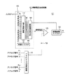
図3は、マイコンで使用される、従来の逐次比較型A/Dコンバータの構成を示している。A/Dコンバータ30に外部から入力される基準電圧AVREFは、ラダー抵抗網35によって(N+1)個に等分割され(N=2n−1)、N個の端子を経由して参照電圧生成回路32に入力される。参照電圧生成回路32は、所定の手順に従ってN個の電圧から1つの電圧を順次に選択し、その選択された電圧を参照電圧として順次に出力する。コンパレータ33は、A/Dコンバータ30に入力するアナログ信号の電圧と、参照電圧生成回路32から順次に入力される参照電圧とを逐次比較し、その比較の結果として入力アナログ電圧と等しい参照電圧に対応するデジタル値を変換結果レジスタ34にセットする。
FIG. 3 shows a configuration of a conventional successive approximation A / D converter used in a microcomputer. The reference voltage AVREF input from the outside to the A /
図3に示す従来構成では、A/Dコンバータ30には、参照電圧生成のために使用される専用の基準電圧AVREFが外部から入力されており、この場合、測定するアナログ電圧範囲に応じた基準電圧AVREFを入力すれば、その範囲で高精度なA/D変換が可能である。図3の構成において、専用の基準電圧AVREFを入力する代わりに、基準電圧として、マイコン自体の電源電圧(VDD)を利用することも可能である。この場合には、基準電圧がマイコンの電源電圧VDDと同じ電位であるため、使用できる参照電圧の範囲が限られるものの、測定における分解能を落とせば、ある程度必要なアナログ電圧のA/D変換が可能である。
In the conventional configuration shown in FIG. 3, a dedicated reference voltage AVREF used for generating a reference voltage is input to the A /
基準電圧として、図3のようにAVREF電位とゼロ電位とを入力する構成に限らず、正のAVREF電位及び負の−AVREF電位をラダー抵抗網35の両端に入力することもでき、また、測定するアナログ電圧の範囲に応じてこれら基準電圧AVREF、−AVREFを可変とすれば、その範囲で高精度なA/D変換が可能である。
The reference voltage is not limited to the configuration in which the AVREF potential and the zero potential are input as shown in FIG. 3, and a positive AVREF potential and a negative -AVREF potential can be input to both ends of the
図4に示す従来のA/Dコンバータ30Aは、図3の従来のA/Dコンバータ30の構成に加えて、内部に基準電圧AVREFを生成する降圧回路36を備えおり、降圧回路36は、マイコンの電源電圧VDDを降圧して、基準電圧AVREFをラダー抵抗網35に入力している。図4の構成によると、降圧回路を36を備えるため、回路規模が大きくなり、低コストのA/D変換器の実現が困難である。また、この方式では、内部で生成する基準電圧AVREFの精度が、A/Dコンバータ30Aの変換精度に直接的に影響し、高精度でのA/D変換が難しいという問題がある。
A conventional A /
上記各従来のA/Dコンバータでは、参照電圧生成回路が生成する参照電圧の範囲は、基準電圧AVREFによって定まり、基準電圧AVREFを可変としない限り、入力されるアナログ電圧のレベルが異なると、A/D変換が不可能となり、或いは、A/D変換自体は可能であっても、必要な分解能が得られないという問題がある。 In each of the conventional A / D converters described above, the range of the reference voltage generated by the reference voltage generation circuit is determined by the reference voltage AVREF, and if the level of the input analog voltage is different unless the reference voltage AVREF is variable, There is a problem that / D conversion becomes impossible, or even if A / D conversion itself is possible, a necessary resolution cannot be obtained.
特許文献1には、入力する基準電圧を一定として、使用する参照電圧の変化回数を制御するA/Dコンバータが記載されている。図5にそのA/Dコンバータの構成を示す。このA/Dコンバータ40では、A/D変換に際して分解能を指定する分解能指定レジスタ46を有しており、分解能指定レジスタ46の出力は、制御回路41に入力されている。制御回路41は、参照電圧生成回路42からコンパレータ43に入力される参照電圧の変化回数を、分解能指定レジスタ46によって指定された分解能によって制御する。この場合、指定された分解能が高ければ、参照電圧の変化回数が多くなり、逆に指定された分解能が低ければ、参照電圧の変化回数が少なくなる。この構成により、分解能が低くてよい場合には、参照電圧の変化回数を少なくしてA/D変換における変換速度を上げ、また、高い分解能が要求される場合には、参照電圧の変化回数を多くして必要な分解能を確保している。
上記公報に記載の技術では、参照電圧の変化回数を制御して、A/D変換に必要な高い分解能又は高速なA/D変換の何れかを選択可能である。しかし、該公報に記載のA/Dコンバータ40は、参照電圧の変化範囲を制御するものではなく、従って、アナログ信号が様々な電圧レベルをとるときには、必要な変換精度を保ちながらA/D変換をすることが出来ない。
In the technique described in the above publication, it is possible to select either high resolution required for A / D conversion or high-speed A / D conversion by controlling the number of changes of the reference voltage. However, the A /
本発明の目的は、入力アナログ信号の電圧範囲が様々なレベルにあっても、必要な分解能を確保しつつA/D変換が可能なA/Dコンバータを提供することにある。 An object of the present invention is to provide an A / D converter capable of A / D conversion while ensuring a necessary resolution even when the voltage range of an input analog signal is at various levels.
上記目的を達成するために、本発明のA/Dコンバータは、入力アナログ信号の電圧と参照電圧との大小を比較して前記入力アナログ信号をデジタル信号に変換するA/Dコンバータにおいて、
基準電圧を分割してN個の端子から分割電圧として出力する電圧分割部と、
前記電圧分割部のN個の端子から、連続するM個の端子(N>M)を選択し、該M個の端子の分割電圧を、前記参照電圧として出力する参照電圧出力部とを備えることを特徴とする。
In order to achieve the above object, an A / D converter according to the present invention is an A / D converter that compares the voltage of an input analog signal with a reference voltage to convert the input analog signal into a digital signal.
A voltage divider that divides the reference voltage and outputs the divided voltage from N terminals as a divided voltage;
A reference voltage output unit configured to select M consecutive terminals (N> M) from the N terminals of the voltage dividing unit and to output the divided voltage of the M terminals as the reference voltage; It is characterized by.
本発明のA/Dコンバータによると、入力アナログ信号が様々な電圧範囲にあっても、入力アナログ電圧に適合した参照電圧をコンパレータに入力することができるので、必要な分解能を保ちつつ様々な電圧範囲の入力アナログ信号をデジタル値に変換可能である。 According to the A / D converter of the present invention, even when the input analog signal is in various voltage ranges, a reference voltage suitable for the input analog voltage can be input to the comparator, so that various voltages can be maintained while maintaining the necessary resolution. A range of input analog signals can be converted to a digital value.
本発明の好ましい態様のA/Dコンバータでは、前記参照電圧出力部が、ソフトウエアによって指定されたM個の端子を選択する。また、入力アナログ信号と、選択すべきM個の端子とを関連付けて記憶する記憶部を備えることも本発明の好ましい態様である。 In the A / D converter according to a preferred aspect of the present invention, the reference voltage output unit selects M terminals designated by software. It is also a preferable aspect of the present invention to include a storage unit that stores an input analog signal and M terminals to be selected in association with each other.
以下、図面を参照し、本発明の実施形態例に基づいて、本発明を更に詳細に説明する。図1は、本発明の第1の実施形態例に係るA/Dコンバータの構成を示すブロック図であり、本実施形態例のA/Dコンバータ10は、逐次比較型のA/Dコンバータとして構成される。
Hereinafter, with reference to the drawings, the present invention will be described in more detail based on exemplary embodiments of the present invention. FIG. 1 is a block diagram showing a configuration of an A / D converter according to a first embodiment of the present invention. An A /
A/Dコンバータ10は、複数のポートP1〜Psを経由してそれぞれ入力されるアナログ入力信号の内からA/D変換すべき1つのアナログ信号を選択するアナログ入力選択回路11と、基準電圧AVREFから所望の参照電圧を生成して出力する参照電圧生成回路12と、アナログ入力選択回路11によって選択されたアナログ信号をサンプリングコンデンサ19を介して受信し、受信したアナログ信号の電圧値と参照電圧生成回路12によって生成された参照電圧とを逐次比較するコンパレータ13と、コンパレータ13の比較結果として決定されたアナログ信号の電圧レベルに対応する参照電圧のデジタル値をラッチし格納する変換結果レジスタ14とを備える。変換結果レジスタは、Nビットのレジスタとして構成されている。
The A /
参照電圧生成回路12は、基準電圧をN個に分割するラダー抵抗網15と、ラダー抵抗網15のN個の端子の内から選択すべき連続するM個の端子を指定する信号を記憶する制御レジスタ16と、N個の端子から制御レジスタ16が指定する連続するM個の端子を選択する端子選択回路17と、アップダウンカウンタ及びシフトレジスタを内蔵し、端子選択回路17で選択されたM個の端子からコンパレータ13の参照入力(−)に入力すべき端子を逐次選択する参照電圧出力部18とを備える。端子選択回路17は、例えば、M個の出力端子に対応して配設される、N/M入力−1出力、又は、2N/M入力−1出力のM個のマルチプレクサから構成される。
The reference voltage generation circuit 12 stores a signal that specifies a
図1のA/Dコンバータ10では、基準電圧AVREFが抵抗ラダー網15によってN個の電圧値に分圧されており、各分圧は対応するN個の端子を経由して端子選択回路17に入力されている。ここで、各アナログ信号は、0V〜AVREFのフルレンジではなく、特定の電圧範囲内で振れるものであり、制御レジスタ16に格納される信号が、その特定の電圧範囲に対応した電圧値を出力するM個の端子が選択できるように、各アナログ信号毎に決定される。
In the A /
動作にあたって、アナログ入力選択回路11がA/D変換すべきアナログ信号を1つ選択する。その選択されたアナログ信号が持つ電圧範囲に対応して定められた選択信号が制御レジスタ16から端子選択回路17に入力される。端子選択回路17は、その選択信号に応答してN個の端子から連続するM個の端子を選択する。ここで、N=2n−1、M=2m−1である。例えば、nは12、mは10である。この場合、本実施形態例のA/D変換器10では、参照電圧の変化回数を10ビットの分解能と同じ変化回数に抑えることで、コンパレータ13における比較を高速に行いながらも、12ビットの分解能でA/D変換を可能とする。つまり、高分解能で且つ高速なA/D変換が可能である。
In operation, the analog input selection circuit 11 selects one analog signal to be A / D converted. A selection signal determined corresponding to the voltage range of the selected analog signal is input from the
参照電圧出力部18は、アップダウンカウンタ及びシフトレジスタを有し、これらによって、M個の端子を経由して入力する電圧から、コンパレータ13で比較すべき参照電圧を順次に選択する。参照電圧出力部18は、選択された参照電圧をコンパレータ13に順次に入力する。まず、mビットの内でMSBのビットに相当する参照電圧が選択され、この参照電圧がコンパレータ13において、入力アナログ信号の電圧値と比較される。その比較結果に基づいて、デジタル信号のMSBが「0」又は「1」に決定される。参照電圧出力部18は、変換結果レジスタ14に向けて、選択した参照電圧を特定する信号を送信する。その結果、比較結果レジスタ14には、選択された参照電圧に対応するビットに、コンパレータ13の出力に基づいて「0」又は「1」が格納される。以下、順次に、次のビットからLSBまでが決定され、その結果が、nビット構成の比較結果レジスタ14の内のmビットに順次に格納される。比較結果レジスタ14は、nビットの内で、端子選択回路17で選択されたM個の端子に対応するm個のビット以外の各ビットには、全て「0」が格納される。これによって、選択された入力アナログ信号の電圧値がnビットのデジタル信号に変換される。
The reference
次の入力アナログ信号が選択されると、その選択されたアナログ信号の電圧範囲に対応した連続するM個の端子が、端子選択回路17によって選択される。このように、選択される個々のアナログ信号に対応して参照電圧の範囲が選択できるので、分解能を所望の値に維持しながらも、異なる電圧範囲のアナログ信号がA/D変換可能である。
When the next input analog signal is selected, the
図2は、本発明の第2の実施形態例に係るA/Dコンバータのブロック図であり、このA/Dコンバータ20は、直接比較型(フラッシュ型)A/Dコンバータとして構成される。A/Dコンバータ20は、複数のポートP1〜Psを経由してそれぞれ入力されるアナログ入力信号の内からA/D変換すべき1つのアナログ信号を選択するアナログ入力選択回路21と、基準電圧AVREFを分割してN個の端子から分割電圧を出力するラダー抵抗網22と、N個の端子から連続するM個の端子を選択する端子選択回路23と、アナログ入力選択回路21によって選択されたアナログ信号を受信し、そのアナログ信号の電圧値と端子選択回路23によって生成されたM個の参照電圧とを直接に比較する多数のコンパレータから成るコンパレータアレイ24と、コンパレータアレイ24の比較結果をM進/2進変換するM進2進変換器25と、M進2進変換器25の出力をラッチし、これをnビットの電圧信号として格納する変換結果レジスタ26とを備える。
FIG. 2 is a block diagram of an A / D converter according to the second embodiment of the present invention, and the A /
動作にあたって、アナログ入力選択回路21が、A/D変換すべきアナログ信号を1つ選択する。その選択されたアナログ信号が持つ電圧範囲に対応して定められた選択信号が制御レジスタ27から端子選択回路23に入力される。端子選択回路23は、その選択信号に応答してN個の端子から連続するM個の端子を選択する。
In operation, the analog
端子選択回路23で選択されたM個の参照電圧は、コンパレータアレイ24のM個のコンパレータのそれぞれに入力される。各コンパレータは、選択された入力アナログ信号の電圧値と、各コンパレータに対応する参照電圧とを比較し、その比較結果を「0」又は「1」として出力する。M個のコンパレータの内、入力アナログ信号の電圧よりも高い参照電圧に対応するコンパレータの出力は全て「0」に、入力アナログ信号の電圧よりも低い参照電圧に対応するコンパレータの出力は全て「1」になる。M進2進変換器は、出力が「1」になった最も上位のコンパレータを特定して、そのコンパレータに付けられたシーケンシャル番号をM進/2進変換する。
The M reference voltages selected by the
変換結果レジスタ25には、選択されたM個の端子を特定する信号が制御レジスタ27から送られており、変換結果レジスタ25は、M進2進変換器25から入力した2進数の数値をセットしたビット以外のビットに「0」をセットし、これによって、nビットの電圧値を格納する。
A signal specifying the selected M terminals is sent from the
次の入力アナログ信号が選択されると、その選択されたアナログ信号の電圧範囲に対応した連続するM個の端子が、端子選択回路32によって、N個の端子から選択される。このように、選択されるアナログ信号に対応して参照電圧の電圧範囲が選択できるので、分解能を所望の値に維持しながら、異なる電圧範囲のアナログ信号がA/D変換可能である。本実施形態例のA/D変換器によると、mビット構成の簡素なコンパレータアレイを使用しながらも、nビットの分解能でアナログ信号のA/D変換が可能である。
When the next input analog signal is selected, consecutive M terminals corresponding to the voltage range of the selected analog signal are selected from the N terminals by the
上記各実施形態例のA/D変換器では、任意の電圧範囲のアナログ信号のA/D変換を、高分解能で且つ低コストで実現することが出来る。 In the A / D converters of the above embodiments, A / D conversion of analog signals in an arbitrary voltage range can be realized with high resolution and low cost.
以上、本発明をその好適な実施態様に基づいて説明したが、本発明のA/Dコンバータは、上記実施態様の構成にのみ限定されるものではなく、上記実施態様の構成から種々の修正及び変更を施したものも、本発明の範囲に含まれる。例えば本発明のA/D変換器は、基準電圧を分割する電圧分割部を有するA/D変換器であればよく、A/D変換器の型式は如何なるものでもよい。また、分割数や参照電圧の数は単に例示であり、入力アナログ信号に対応して所望の数が選択できる。 Although the present invention has been described based on the preferred embodiment, the A / D converter of the present invention is not limited to the configuration of the above embodiment, and various modifications and changes can be made to the configuration of the above embodiment. Changes are also included in the scope of the present invention. For example, the A / D converter of the present invention may be an A / D converter having a voltage dividing unit that divides a reference voltage, and any type of A / D converter may be used. Further, the number of divisions and the number of reference voltages are merely examples, and a desired number can be selected corresponding to the input analog signal.
10:A/Dコンバータ
11:アナログ入力選択回路
12:参照電圧生成回路
13:コンパレータ
14:変換結果レジスタ
15:ラダー抵抗網
16:制御レジスタ
17:端子選択回路
18:参照電圧出力部
19:サンプリングコンデンサ
20:A/Dコンバータ
21:アナログ入力選択回路
22:ラダー抵抗網
23:端子選択回路
24:コンパレータアレイ
25:M進2進変換器
26:変換結果レジスタ
27:制御レジスタ
10: A / D converter 11: Analog input selection circuit 12: Reference voltage generation circuit 13: Comparator 14: Conversion result register 15: Ladder resistor network 16: Control register 17: Terminal selection circuit 18: Reference voltage output unit 19: Sampling capacitor 20: A / D converter 21: Analog input selection circuit 22: Ladder resistor network 23: Terminal selection circuit 24: Comparator array 25: M-ary binary converter 26: Conversion result register 27: Control register
Claims (4)
基準電圧を分割してN個の端子から分割電圧として出力する電圧分割部と、
前記電圧分割部のN個の端子から、連続するM個の端子(N>M)を選択し、当該M個の端子の分割電圧をM個の前記参照電圧とし、当該M個から1個を選択して前記参照電圧として出力する参照電圧出力部とを備え、
前記1個の参照電圧の選択と、前記入力アナログ信号電圧と前記選択された前記参照電圧との比較とを、m回(mはM=2 m −1を満たす整数)行うことで、mビットの変換結果を生成することを特徴とするA/Dコンバータ。 In the A / D converter that compares the voltage of the input analog signal with the reference voltage and converts the input analog signal into a digital signal,
A voltage divider that divides the reference voltage and outputs the divided voltage from N terminals as a divided voltage;
From the N terminal of the voltage divider unit, and selects M terminal successive (N> M), a division voltage of the M-number of terminals and the M of the reference voltage, the one from the M pieces A reference voltage output unit that selects and outputs the reference voltage,
By selecting the one reference voltage and comparing the input analog signal voltage with the selected reference voltage m times (m is an integer satisfying M = 2 m −1), m bits are obtained. An A / D converter characterized by generating a conversion result.
前記A/Dコンバータは、前記mビットの変換結果と、(n−m)個の各ビットを0値としたものとを前記nビットの変換結果レジスタに格納する請求項1から3までの何れか一項に記載のA/Dコンバータ。 4. The A / D converter according to claim 1, wherein the A / D converter stores the m-bit conversion result and the (n−m) bits each having a zero value in the n-bit conversion result register. The A / D converter according to claim 1.
Priority Applications (1)
| Application Number | Priority Date | Filing Date | Title |
|---|---|---|---|
| JP2004025713A JP4519475B2 (en) | 2004-02-02 | 2004-02-02 | A / D converter |
Applications Claiming Priority (1)
| Application Number | Priority Date | Filing Date | Title |
|---|---|---|---|
| JP2004025713A JP4519475B2 (en) | 2004-02-02 | 2004-02-02 | A / D converter |
Publications (2)
| Publication Number | Publication Date |
|---|---|
| JP2005218044A JP2005218044A (en) | 2005-08-11 |
| JP4519475B2 true JP4519475B2 (en) | 2010-08-04 |
Family
ID=34908023
Family Applications (1)
| Application Number | Title | Priority Date | Filing Date |
|---|---|---|---|
| JP2004025713A Expired - Fee Related JP4519475B2 (en) | 2004-02-02 | 2004-02-02 | A / D converter |
Country Status (1)
| Country | Link |
|---|---|
| JP (1) | JP4519475B2 (en) |
Families Citing this family (1)
| Publication number | Priority date | Publication date | Assignee | Title |
|---|---|---|---|---|
| JP6287433B2 (en) | 2014-03-25 | 2018-03-07 | セイコーエプソン株式会社 | Successive comparison type analog-digital converter, physical quantity detection sensor, electronic device and moving body, and successive comparison type analog-digital conversion method |
Citations (6)
| Publication number | Priority date | Publication date | Assignee | Title |
|---|---|---|---|---|
| JPS57131123A (en) * | 1980-10-15 | 1982-08-13 | Jido Keisoku Gijutsu Kenkiyuukumiai | Analog-to-digital converter |
| JPS6153830A (en) * | 1984-08-22 | 1986-03-17 | Fujitsu Ltd | analog digital converter |
| JPH01309416A (en) * | 1988-06-07 | 1989-12-13 | Matsushita Electric Ind Co Ltd | Analog/digital converter |
| JPH04170225A (en) * | 1990-11-02 | 1992-06-17 | Nec Corp | A/d converter |
| JPH05167448A (en) * | 1991-12-18 | 1993-07-02 | Mitsubishi Electric Corp | A/d converter |
| JPH07226683A (en) * | 1994-02-10 | 1995-08-22 | Fujitsu General Ltd | A/d converter |
-
2004
- 2004-02-02 JP JP2004025713A patent/JP4519475B2/en not_active Expired - Fee Related
Patent Citations (6)
| Publication number | Priority date | Publication date | Assignee | Title |
|---|---|---|---|---|
| JPS57131123A (en) * | 1980-10-15 | 1982-08-13 | Jido Keisoku Gijutsu Kenkiyuukumiai | Analog-to-digital converter |
| JPS6153830A (en) * | 1984-08-22 | 1986-03-17 | Fujitsu Ltd | analog digital converter |
| JPH01309416A (en) * | 1988-06-07 | 1989-12-13 | Matsushita Electric Ind Co Ltd | Analog/digital converter |
| JPH04170225A (en) * | 1990-11-02 | 1992-06-17 | Nec Corp | A/d converter |
| JPH05167448A (en) * | 1991-12-18 | 1993-07-02 | Mitsubishi Electric Corp | A/d converter |
| JPH07226683A (en) * | 1994-02-10 | 1995-08-22 | Fujitsu General Ltd | A/d converter |
Also Published As
| Publication number | Publication date |
|---|---|
| JP2005218044A (en) | 2005-08-11 |
Similar Documents
| Publication | Publication Date | Title |
|---|---|---|
| CN107135000B (en) | Capacitor order determination in an analog-to-digital converter | |
| US20050001747A1 (en) | All-analog calibration of string-DAC linearity: application to high voltage processes | |
| KR102636356B1 (en) | Method and apparatus for offset correction in SAR ADC using reduced capacitor array DAC | |
| US8542144B2 (en) | Analog to digital converter | |
| US8902092B2 (en) | Analog-digital conversion circuit and method | |
| US6507296B1 (en) | Current source calibration circuit | |
| JP4263050B2 (en) | Successive approximation type A / D converter | |
| US7579973B2 (en) | Analog-to-digital converter | |
| US6633247B2 (en) | Logarithmic a/d converter, method of logarithmic a/d conversion logarithmic d/a converter, method of logarithmic d/a conversion, and system for measuring physical quantity | |
| JP4519475B2 (en) | A / D converter | |
| JP4613929B2 (en) | A / D conversion circuit | |
| JP7499742B2 (en) | Power supply circuit and voltage detection circuit | |
| JPH04314210A (en) | A/d converter | |
| KR102242402B1 (en) | Method of converting analog signal to digital information having a plurality of bits | |
| JP5190014B2 (en) | Integrating AD conversion circuit and AD conversion method | |
| JP3518514B6 (en) | Logarithmic A / D converter, logarithmic A / D conversion method, and logarithmic D / A converter, | |
| JP2004289759A (en) | A/d converter | |
| JP2002319863A (en) | Analog/digital converter | |
| JP4536498B2 (en) | Analog to digital converter | |
| JP6800545B2 (en) | AD conversion device and AD conversion method | |
| JP3518514B2 (en) | Logarithmic A / D converter, logarithmic A / D conversion method, and logarithmic D / A converter, | |
| Kobayashi et al. | Redundant SAR ADC Algorithms for Reliability Based on Number Theory | |
| JP3114795B2 (en) | High-speed AD converter | |
| KR20090071705A (en) | Analog-to-Digital Converter Using Reference Voltage Selection Circuit | |
| JP2003179491A (en) | A/d converter |
Legal Events
| Date | Code | Title | Description |
|---|---|---|---|
| A621 | Written request for application examination |
Free format text: JAPANESE INTERMEDIATE CODE: A621 Effective date: 20061205 |
|
| A977 | Report on retrieval |
Free format text: JAPANESE INTERMEDIATE CODE: A971007 Effective date: 20090407 |
|
| A131 | Notification of reasons for refusal |
Free format text: JAPANESE INTERMEDIATE CODE: A131 Effective date: 20090416 |
|
| A521 | Written amendment |
Free format text: JAPANESE INTERMEDIATE CODE: A523 Effective date: 20090604 |
|
| A131 | Notification of reasons for refusal |
Free format text: JAPANESE INTERMEDIATE CODE: A131 Effective date: 20090817 |
|
| A521 | Written amendment |
Free format text: JAPANESE INTERMEDIATE CODE: A523 Effective date: 20091009 |
|
| RD01 | Notification of change of attorney |
Free format text: JAPANESE INTERMEDIATE CODE: A7421 Effective date: 20100217 |
|
| TRDD | Decision of grant or rejection written | ||
| A01 | Written decision to grant a patent or to grant a registration (utility model) |
Free format text: JAPANESE INTERMEDIATE CODE: A01 Effective date: 20100428 |
|
| A01 | Written decision to grant a patent or to grant a registration (utility model) |
Free format text: JAPANESE INTERMEDIATE CODE: A01 |
|
| A61 | First payment of annual fees (during grant procedure) |
Free format text: JAPANESE INTERMEDIATE CODE: A61 Effective date: 20100519 |
|
| FPAY | Renewal fee payment (event date is renewal date of database) |
Free format text: PAYMENT UNTIL: 20130528 Year of fee payment: 3 |
|
| R150 | Certificate of patent or registration of utility model |
Free format text: JAPANESE INTERMEDIATE CODE: R150 |
|
| LAPS | Cancellation because of no payment of annual fees |