JP4513289B2 - ELECTRO-OPTICAL DEVICE, ELECTRONIC DEVICE, AND POWER CONTROL METHOD FOR ELECTRO-OPTICAL DEVICE - Google Patents
ELECTRO-OPTICAL DEVICE, ELECTRONIC DEVICE, AND POWER CONTROL METHOD FOR ELECTRO-OPTICAL DEVICE Download PDFInfo
- Publication number
- JP4513289B2 JP4513289B2 JP2003299073A JP2003299073A JP4513289B2 JP 4513289 B2 JP4513289 B2 JP 4513289B2 JP 2003299073 A JP2003299073 A JP 2003299073A JP 2003299073 A JP2003299073 A JP 2003299073A JP 4513289 B2 JP4513289 B2 JP 4513289B2
- Authority
- JP
- Japan
- Prior art keywords
- voltage
- power supply
- electro
- scanning
- optical device
- Prior art date
- Legal status (The legal status is an assumption and is not a legal conclusion. Google has not performed a legal analysis and makes no representation as to the accuracy of the status listed.)
- Expired - Fee Related
Links
Images


Landscapes
- Liquid Crystal (AREA)
- Liquid Crystal Display Device Control (AREA)
- Control Of Indicators Other Than Cathode Ray Tubes (AREA)
Description
本発明は、電気光学装置、電子機器、及び電気光学装置の電源制御方法に関する。 The present invention relates to an electro-optical device, an electronic apparatus, and a power control method for the electro-optical device.
表示装置、例えば、電気光学材料として液晶を用いた液晶表示装置は、陰極線管(CRT)に代わるディスプレイデバイスとして、各種情報処理機器の表示部や液晶テレビなどに広く用いられている。 A display device, for example, a liquid crystal display device using a liquid crystal as an electro-optical material, is widely used as a display device in place of a cathode ray tube (CRT) in a display unit of various information processing devices, a liquid crystal television, and the like.
液晶表示装置は、液晶パネルと周辺回路を備える。液晶パネルには、マトリクス状に配列した画素電極と、この画素電極に接続されたTFT(Thin Film Transistor:薄膜トランジスタ)のようなスイッチング素子などが設けられた素子基板と、画素電極に対向する対向電極が形成された対向基板と、これら両基板との間に充填された電気光学材料たる液晶とを備える。画素は、スイッチング素子、画素電極、電気光学材料及び対向電極によって構成され、マトリクス状に配置される。また、液晶パネルには、走査線駆動回路が形成され、走査線は走査線駆動回路から順次出力される各走査信号に応じて選択される。 The liquid crystal display device includes a liquid crystal panel and a peripheral circuit. The liquid crystal panel includes a pixel electrode arranged in a matrix, an element substrate provided with a switching element such as a TFT (Thin Film Transistor) connected to the pixel electrode, and a counter electrode facing the pixel electrode. And a liquid crystal which is an electro-optic material filled between the two substrates. A pixel is composed of a switching element, a pixel electrode, an electro-optic material, and a counter electrode, and is arranged in a matrix. Further, a scanning line driving circuit is formed in the liquid crystal panel, and the scanning line is selected according to each scanning signal sequentially output from the scanning line driving circuit.
液晶表示装置において、周辺回路のロジック系の電源と液晶パネルへ給電されるLCD系の電源とは、別系統で設けられている。そして、ロジック系の電源を投入した後、LCD系の電源を投入する技術が知られている(例えば、特許文献1)。また、液晶パネルのインタフェースである受信回路の動作が安定した後、LCD系の電源を投入する技術も公知である(例えば、特許文献2)。 In the liquid crystal display device, the logic system power source of the peripheral circuit and the LCD system power source fed to the liquid crystal panel are provided in different systems. A technique for turning on the LCD system after turning on the logic system is known (for example, Patent Document 1). In addition, a technique of turning on the LCD system after the operation of the receiving circuit which is an interface of the liquid crystal panel is stabilized is also known (for example, Patent Document 2).
ところで、走査線駆動回路には、シフトレジスタとレベルシフタとを備えるものがある。レベルシフタは、シフトレジスタによって転送されたパルスを大振幅に変換して走査信号として出力する。この場合、シフトレジスタとレベルシフタは別系統の電源によって動作する。つまり、液晶パネルには複数系統の電源が供給される。 Meanwhile, some scanning line driving circuits include a shift register and a level shifter. The level shifter converts the pulse transferred by the shift register into a large amplitude and outputs it as a scanning signal. In this case, the shift register and the level shifter are operated by different power sources. That is, a plurality of systems of power are supplied to the liquid crystal panel.
しかしながら、従来の液晶表示装置においては、液晶パネルに供給する電源を一つの系統とみなして、それら全体をオン・オフするといった制御がなされている。このため、起動時の電流量が大きくなるといった問題があった。また、液晶パネルに電源が投入された時点で、走査線駆動回路のシフトレジスタの各段において、各出力信号がアクティブになるか非アクティブになるかは、シフトレジスタを構成するトランジスタのゲート電位に依存するため、一意に定まる分けではない。このため、電源投入時に複数の走査線が選択されることもあるので、起動時の画面が乱れるといった問題があった。 However, in the conventional liquid crystal display device, the power supplied to the liquid crystal panel is regarded as one system, and control is performed to turn them all on and off. For this reason, there has been a problem that the amount of current at the time of startup becomes large. In addition, when power is supplied to the liquid crystal panel, whether each output signal becomes active or inactive at each stage of the shift register of the scanning line driver circuit depends on the gate potential of the transistor constituting the shift register. Because it depends, it is not a unique division. For this reason, since a plurality of scanning lines may be selected when the power is turned on, there is a problem that the screen at the time of startup is disturbed.
そこで、本発明は、起動時の電流を低減し、且つ、起動時の表示画像の乱れを防止する電気光学装置、電子機器、及び電気光学装置の電源制御方法を提供することを解決課題とする。 SUMMARY OF THE INVENTION Accordingly, it is an object of the present invention to provide an electro-optical device, an electronic apparatus, and a power control method for the electro-optical device that reduce a current at startup and prevent disturbance of a display image at startup. .
上述した課題を解決するため、本発明に係る電気光学装置は、複数のデータ線、複数の走査線、及び前記データ線と前記走査線との交差に対応して設けられた複数のスイッチング素子と、各スイッチング素子に接続される複数の画素電極と、前記各走査線を駆動する各走査信号を順次出力する走査線駆動回路を備えたものであって、前記走査線駆動回路は、第1電源の給電を受けて転送開始パルスを順次シフトするシフトレジスタと、第2電源の給電を受けて前記シフトレジスタの出力信号のレベルを変換して前記各走査信号を出力するレベルシフタとを備え、前記第1電源と前記第2電源とを生成する電源手段と、前記第1電源を立ち上げた後、前記第2電源を立ち上げるように前記電源手段を制御する制御手段と、を備えることを特徴とする。 In order to solve the above-described problem, an electro-optical device according to the present invention includes a plurality of data lines, a plurality of scanning lines, and a plurality of switching elements provided corresponding to intersections of the data lines and the scanning lines. And a plurality of pixel electrodes connected to each switching element and a scanning line driving circuit for sequentially outputting each scanning signal for driving each scanning line, wherein the scanning line driving circuit includes a first power source. A shift register that sequentially shifts the transfer start pulse by receiving power from the second power supply, and a level shifter that receives power from the second power source and converts the level of the output signal of the shift register to output the respective scanning signals. Power supply means for generating one power supply and the second power supply, and control means for controlling the power supply means to start up the second power supply after the first power supply is turned on. That.
この発明によれば、走査線駆動回路のシフトレジスタに第1電源を投入した後に、レベルシフタに第2電源を投入することができる。このため、シフトレジスタとレベルシフタとは段階的に起動するから、起動時における電流を低減することが可能となる。また、走査信号はレベルシフタから出力されるが、シフトレジスタが正常に動作するまでの期間は、レベルシフタを動作させても異常な走査信号が出力される可能性がある。従って、制御手段は、第1電源の立ち上げからシフトレジスタが正常の動作するまでの所定の期間が経過した後、第2電源を立ち上げるように電源手段を制御することが好ましい。 According to the present invention, it is possible to turn on the second power supply to the level shifter after turning on the first power supply to the shift register of the scanning line driving circuit. For this reason, since the shift register and the level shifter are activated in stages, the current at the time of activation can be reduced. Further, although the scanning signal is output from the level shifter, an abnormal scanning signal may be output even if the level shifter is operated until the shift register operates normally. Therefore, it is preferable that the control means controls the power supply means to start up the second power supply after a predetermined period from when the first power supply is turned on until the shift register operates normally.
上述した電気光学装置において、前記第2電源の電圧は、前記第1電源の電圧よりも高電圧であることが好ましい。これにより、スイッチング素子のオン・オフが制御できるように走査線を大振幅で駆動することが可能となり、且つ、シフトレジスタの消費電流を低減することが可能となる。 In the electro-optical device described above, it is preferable that the voltage of the second power supply is higher than the voltage of the first power supply. As a result, the scanning line can be driven with a large amplitude so that the on / off state of the switching element can be controlled, and the current consumption of the shift register can be reduced.
上述した電気光学装置において、前記制御手段は、前記第1電源を立ち上げてから少なくとも1フレーム期間が経過した後に前記第2電源を立ち上げるように前記電源手段を制御することが好ましい。起動時において、シフトレジスタの各段から出力される信号の論理レベルはシフトレジスタを構成するトランジスタのゲート電位に依存するため、一意に定まる分けではない。従って、シフトレジスタとレベルシフタの電源を同時に立ち上げると、複数の走査線が同時に選択され、大電流が流れるとともに異常な画面が表示されてしまう。一方、1フレーム期間の経過によってシフトレジスタは正常に初期化される。この発明によれば、第1電源の投入から少なくとも1フレーム期間が経過した後に第2電源が投入されるので、起動時における画面の異常を防止し、且つ、電流を低減することができる。これにより、電気光学パネル及び電源手段の負荷を軽減することができる。 In the electro-optical device described above, it is preferable that the control unit controls the power source unit so that the second power source is started after at least one frame period has elapsed since the first power source was started. At startup, the logic level of the signal output from each stage of the shift register depends on the gate potential of the transistors constituting the shift register, and is not uniquely determined. Therefore, when the power supply of the shift register and the level shifter is turned on at the same time, a plurality of scanning lines are simultaneously selected, and a large current flows and an abnormal screen is displayed. On the other hand, the shift register is normally initialized as one frame period elapses. According to the present invention, since the second power source is turned on after at least one frame period has elapsed since the first power source was turned on, it is possible to prevent screen abnormalities at startup and to reduce the current. Thereby, the load of the electro-optical panel and the power supply means can be reduced.
より具体的には、上述した電気光学装置において、前記転送開始パルスを前記1フレーム期間毎に生成するタイミング発生手段を備え、前記制御手段は、前記第1電源を立ち上げた後に、前記転送開始パルスを生成する処理を初期化するように前記タイミング発生手段を制御し、初期化後に最初の前記転送開始パルスが生成されてから少なくとも次の前記転送開始パルスが生成された後に前記第2電源を立ち上げるように前記電源手段を制御することが好ましい。 More specifically, in the above-described electro-optical device, the electro-optical device includes a timing generation unit that generates the transfer start pulse for each frame period, and the control unit starts the transfer after the first power supply is turned on. The timing generator is controlled to initialize a process for generating a pulse, and after the first transfer start pulse is generated after the initialization, at least the next transfer start pulse is generated and then the second power supply is turned on. It is preferable to control the power supply means to start up.
また、上述した電気光学装置において、前記データ線、前記走査線、前記スイッチング素子、及び前記画素電極が形成された素子基板と、対向電極が形成された対向基板と、前記素子基板と前記対向電極と間隙に電気光学材料を備え、前記電源手段は、前記対向電極に対向電極電位を供給し、前記制御手段は、電源手段は、前記対向電極電位を前記第2電源の立ち上げと同時に供給するように前記電源手段を制御することが好ましい。電気光学装置における階調表示は、電気光学材料(例えば、液晶)に印加される電圧によって定まることがある。この場合には、対向電極に何らかの電位を与えて、電気光学材料に電圧を印加する必要がある。しかしながら、走査線が選択されるまでは、対向電極に対向電極電位を引加する必要がない。この発明によれば、第2電源の立ち上げと同時に対向電極電位を立ち上げるので、画像表示の準備が整ってから対向電極電位を供給することができる。特に、ノーマリーブラックモードで動作する場合は、第2電源の立ち上げ前に対向電極をフローティングすることによって画面を暗くし、第2電源の立ち上げと同時に画像を正常に表示することが可能となる。 In the electro-optical device described above, the element substrate on which the data line, the scanning line, the switching element, and the pixel electrode are formed, the counter substrate on which the counter electrode is formed, the element substrate, and the counter electrode An electro-optic material in the gap, the power supply means supplies a counter electrode potential to the counter electrode, and the control means supplies the counter electrode potential simultaneously with the start-up of the second power supply. It is preferable to control the power supply means. The gradation display in the electro-optical device may be determined by a voltage applied to an electro-optical material (for example, liquid crystal). In this case, it is necessary to apply some potential to the counter electrode and apply a voltage to the electro-optic material. However, it is not necessary to apply the counter electrode potential to the counter electrode until the scanning line is selected. According to the present invention, the counter electrode potential is raised at the same time as the second power supply is turned on, so that the counter electrode potential can be supplied after the preparation for image display is completed. In particular, when operating in normally black mode, it is possible to darken the screen by floating the counter electrode before starting the second power supply, and to display images normally at the same time the second power supply is turned on. Become.
上述した電気光学装置において、前記第2電源は高電位と低電位とを含み、前記電源手段は、前記対向電極電位を所定周期で交流化駆動すると共に、前記第2電源の前記高電位と前記低電位とのうち少なくとも一方を、前記所定周期に同期して交流化駆動することが好ましい。走査線と対向電極との間には寄生容量が存在する。このため、走査線は容量性の負荷である。対向電極電位を交流化駆動する場合には、第2電源の高電位と低電位のうち、走査線を非選択状態にする電位を対向電極と同期して動作させることによって、走査線駆動回路の消費電流を低減することが可能となる。 In the above-described electro-optical device, the second power supply includes a high potential and a low potential, and the power supply unit drives the counter electrode potential to be alternating-currentd at a predetermined cycle, and the high potential of the second power supply It is preferable that at least one of the low potentials is AC driven in synchronization with the predetermined period. There is a parasitic capacitance between the scanning line and the counter electrode. For this reason, the scanning line is a capacitive load. When the counter electrode potential is AC driven, the potential for making the scan line non-selected among the high potential and the low potential of the second power source is operated in synchronization with the counter electrode, thereby It is possible to reduce current consumption.
次に、本発明に係る電子機器は、上述した電気光学装置を備えることを特徴とし、例えば、液晶プロジェクタ、パーソナルコンピュータ、携帯電話、電子カメラ、PDA等が該当する。 Next, an electronic apparatus according to the present invention includes the above-described electro-optical device, and includes, for example, a liquid crystal projector, a personal computer, a mobile phone, an electronic camera, and a PDA.
次に、本発明に係る電気光学装置の電源制御方法は、複数のデータ線、複数の走査線、及び前記データ線と前記走査線との交差に対応して設けられた複数のスイッチング素子と、各スイッチング素子に接続される複数の画素電極と、前記各走査線を駆動する各走査信号を順次出力する走査線駆動回路とを備え、前記走査線駆動回路は、第1電源の給電を受けて転送開始パルスを順次シフトするシフトレジスタと、第2電源の給電を受けて前記シフトレジスタの出力信号のレベルを変換して前記各走査信号を出力するレベルシフタとを備えた電気光学装置を前提とし、前記第1電源を立ち上げた後、前記第2電源を立ち上げることを特徴とする。特に、前記第1電源を立ち上げてから少なくとも1フレーム期間が経過した後に前記第2電源を立ち上げることが、異常画面の表示防止及び起動時の電流低減の観点から好ましい。 Next, the power control method for the electro-optical device according to the present invention includes a plurality of data lines, a plurality of scanning lines, and a plurality of switching elements provided corresponding to intersections of the data lines and the scanning lines, A plurality of pixel electrodes connected to each switching element; and a scanning line driving circuit for sequentially outputting each scanning signal for driving each scanning line, the scanning line driving circuit receiving power from a first power supply Assuming an electro-optical device comprising: a shift register that sequentially shifts transfer start pulses; and a level shifter that receives power from a second power supply and converts the level of an output signal of the shift register to output the scanning signals. The second power supply is started after the first power supply is started. In particular, it is preferable to start up the second power supply after at least one frame period has passed since the start of the first power supply from the viewpoint of preventing display of an abnormal screen and reducing current at startup.
以下、図面を参照して、本発明に係わる実施形態を説明する。なお、本実施形態では、電気光学材料として液晶を用いた液晶パネルを電気光学パネルの一例とし、液晶パネルを用いた液晶表示装置を電気光学装置の一例として説明する。 Embodiments according to the present invention will be described below with reference to the drawings. In the present embodiment, a liquid crystal panel using liquid crystal as an electro-optical material will be described as an example of an electro-optical panel, and a liquid crystal display device using the liquid crystal panel will be described as an example of an electro-optical device.
<1.液晶表示装置の全体構成>
図1に液晶表示装置の全体構成を示す。この図に示すように液晶表示装置は、マイコン10、システム電源回路20、駆動用電源回路30、メインスイッチSW、データ線駆動回路200、及び液晶パネルAAを備える。マイコン10は、液晶表示装置の全体を制御する制御手段として機能する。使用者がメインスイッチSWを操作すると、メインスイッチSWは操作に応じた信号を出力する。システム電源回路20は、この信号に応じて起動して、マイコン10及び駆動用電源回路30にシステム電源VSを供給する。システム電源VSが立ち上がると、マイコン10は、これを検知して、電源起動シーケンスを実行する。
<1. Overall configuration of liquid crystal display device>
FIG. 1 shows the overall configuration of the liquid crystal display device. As shown in this figure, the liquid crystal display device includes a
駆動用電源回路30は、マイコン10の制御の下に、各種の電源電圧を出力する。駆動用電源回路30が出力する電源電圧には、以下のものがある。高電圧電源VHHXY及び低電圧電源VLLXYは、走査線駆動回路100のレベルシフタに供給される。高電圧電源VHHXYは例えば8Vであり、低電圧電源VLLXYは例えば0Vである。ロジック電源VDDXYは走査線駆動回路100のシフトレジスタに供給される。ロジック電源VDDXYは例えば4.8Vである。インターフェース用電源VCCは、走査線駆動回路100及びデータ線駆動回路200のインターフェースに用いられ、例えば、3Vである。また、アナログ電源VDDHSは、データ線駆動回路200のDA変換器に供給され、例えば、4.8Vである。階調基準電源V0及びV15は、DA変換器において各諧調に応じた基準電圧を生成する基準電圧生成回路に用いられる。ロジック電源VDDは、データ線駆動回路200の論理回路に供給され、例えば、2.5Vである。対向電極電位LCCOMは、後述する液晶パネルAAの対向電極に供給される。対応電極電位LCCOMは、一定の電位であってもよいし、あるいは、所定周期で高電位と低電位とに交流化されていてもよい。交流化する場合の高電位は例えば4.6Vであり、低電位は例えば0Vである。
The drive
液晶パネルAAは、走査線駆動回路100と画像表示領域Aを備える。図2に画像表示領域Aの詳細な構成を示す。画像表示領域Aには、m(mは2以上の自然数)本の走査線2が、X方向に沿って平行に配列して形成される一方、n(nは2以上の自然数)本のデータ線3が、Y方向に沿って平行に配列して形成されている。そして、走査線2とデータ線3との交差付近においては、TFT50のゲートが走査線2に接続される一方、TFT50のソースがデータ線3に接続されるとともに、TFT50のドレインが画素電極6に接続される。そして、各画素は、画素電極6と、対向基板に形成される対向電極(後述する)と、これら両電極間に挟持された液晶とによって構成される。この結果、走査線2とデータ線3との各交差に対応して、画素はマトリクス状に配列されることとなる。
The liquid crystal panel AA includes a scanning
また、TFT50のゲートが接続される各走査線2には、走査信号Y1、Y2、…、Ymが、パルス的に線順次で印加されるようになっている。このため、ある走査線2に走査信号が供給されると、当該走査線に接続されるTFT50がオンするので、データ線3から所定のタイミングで供給されるデータ線信号X1、X2、…、Xnは、対応する画素に順番に書き込まれた後、所定の期間保持されることとなる。
Further, scanning signals Y1, Y2,..., Ym are applied to each
各画素に印加される電位レベルに応じて液晶分子の配向や秩序が変化するので、光変調による階調表示が可能となる。例えば、液晶を通過する光量は、ノーマリーホワイトモードであれば、印加電位が高くなるにつれて制限される一方、ノーマリーブラックモードであれば、印加電位が高くなるにつれて緩和されるので、液晶表示装置全体では、画像信号に応じたコントラストを持つ光が各画素毎に出射される。このため、所定の表示が可能となる。 Since the orientation and order of liquid crystal molecules change according to the potential level applied to each pixel, gradation display by light modulation becomes possible. For example, in the normally white mode, the amount of light passing through the liquid crystal is limited as the applied potential is increased. In the normally black mode, the amount of light is reduced as the applied potential is increased. As a whole, light having contrast according to the image signal is emitted for each pixel. For this reason, a predetermined display becomes possible.
図3に走査線駆動回路100の詳細な構成を示す。この図に示すように走査線駆動回路100は、Yシフトレジスタ102及びレベルシフタ103を備える。Yシフトレジスタ102には、ロジック電源VDDXYが供給さる一方、レベルシフタ103には、高電圧電源VHHXYおよび低電圧電源VLLXYが供給される。すなわち、走査線駆動回路100は、複数系統の電源によって駆動される。なお、Yシフトレジスタ102の低電位側の電源は、低電圧電源VLLXYと兼用してもよい。
FIG. 3 shows a detailed configuration of the scanning
Y転送開始パルスDY、Yクロック信号YCKおよび反転Yクロック信号YCKBはYシフトレジスタ102に供給される。Yシフトレジスタ102は、Yクロック信号YCKおよび反転Yクロック信号YCKBに同期して、Y転送開始パルスDYを順次転送して信号y1、y2、…、ymを出力する。
The Y transfer start pulse DY, the Y clock signal YCK, and the inverted Y clock signal YCKB are supplied to the
レベルシフタ103は信号振幅を変換する。レベルシフタ103によって、信号y1、y2、…、ymの信号振幅は、VHHXY−VLLXYに変換される。レベルシフタ103の各出力信号は、走査信号Y1、Y2、…、Ymとして各走査線2に出力される。
The
説明を図1に戻す。データ線駆動回路200は、画像データをデジタル信号からアナログ信号へ変換する複数のDA変換器DACと基準電圧発生回路とを備える。1個のDA変換器DACが1本のデータ線に対応している。一方、基準電圧発生回路は、複数のDA変換器DACに共通している。なお、所定本数のデータ線3に対応してデータ線駆動回路200を複数設けるようにしてもよい。
Returning to FIG. The data line driving
次に、タイミング発生回路300は、マイコン10から供給されるリセット信号Rによって初期化される。タイミング発生回路300は、入力画像データに同期してYクロック信号YCK、反転Yクロック信号YCKB、及びY転送開始パルスDY等の制御信号を生成すると共に、図示せぬ画像処理回路を制御する各種のタイミング信号を生成し、これを出力する。Yクロック信号YCKは、走査線2を選択する期間を特定し、反転Yクロック信号YCKBはYクロック信号YCKの論理レベルを反転したものである。また、Y転送開始パルスDYは、1フレームの先頭でアクティブとなるパルスであって、その周期はフレーム周期と一致する。
Next, the
<2.液晶表示装置の電源起動シーケンス>
次に、液晶表示装置の電源起動シーケンスについて説明する。図4は、マイコン10の制御によって実行される電源起動シーケンスのタイミングチャートである。まず、時刻t1において、システム電源VSが立ち上がると、マイコン10が起動する。マイコン10は、時刻t2において、ロジック電源VDD及びVDDXY、インターフェース用電源VCC、アナログ電源VDDHS、並びに階調基準電源V0及びV15を立ち上げるように駆動用電源回路30を制御する。このうち、ロジック電源VDDXYは、走査線駆動回路100のYシフトレジスタ102に供給される。即ち、走査線駆動回路100においては、まず、レベルシフタ103に先立ってシフトレジスタ102が起動される。また、時刻t2のタイミングでタイミング発生回路300のロジック電源も同時に投入され、Yクロック信号YCK及び反転Yクロック信号YCKBがYシフトレジスタ102に供給される。
<2. Power-on sequence for LCDs>
Next, a power supply startup sequence of the liquid crystal display device will be described. FIG. 4 is a timing chart of a power supply startup sequence executed under the control of the
そして、時刻t3に至ると、マイコン10はリセット信号Rをアクティブにして、タイミング発生回路300を初期化する。この後、時刻t4において、タイミング発生回路300からY転送開始パルスDYが走査線駆動回路100のYシフトレジスタ102に供給される。Yシフトレジスタ102のロジック電源VDDXYは、時刻t2のタイミングで立ち上がるが、このとき、Yシフトレジスタ102を構成する複数の単位シフトレジスタの各出力信号がハイレベルとなるかローレベルとなるかは、確率に左右される。しかしながら、時刻t4においてY転送開始パルスDYが供給され、このパルスがYシフトレジスタ102によって順次転送され、最終段の単位シフトレジスタから出力されると、ロジック電源VDDXYの立ち上り時における異常は解消される。時刻t4において最初に入力されたY転送開始パルスDYは、時刻t4から1フレーム期間1tvが経過した時刻t5において、最終段の単位シフトレジスタから既に出力されている。
Then, at time t3, the
そこで、本実施形態においては、2番目のY転送開始パルスDYがアクティブとなる時刻t5において、高電圧電源VHHXY、低電圧電源VLLXY及び対向電極電位LCCOMを立ち上げている。即ち、Yシフトレジスタ102のロジック電源VDDXYを立ち上げてから少なくとも1フレーム期間が経過した後、レベルシフタ103の高電圧電源VHHXY及び低電圧電源VLLXYが立ち上がる。なお、マイコン10は、2番目のY転送開始パルスDYを検知して、高電圧電源VHHXY及び低電圧電源VLLXYを立ち上げてもよい。
Thus, in the present embodiment, at time t5 when the second Y transfer start pulse DY becomes active, the high voltage power supply VHHXY, the low voltage power supply VLLXY, and the counter electrode potential LCCOM are raised. That is, the high voltage power supply VHHXY and the low voltage power supply VLLXY of the
これにより、Yシフトレジスタ102の起動時の異常が解消された後に、レベルシフタ103が動作して、走査線2が選択されるようになる。このため、ユーザーがメインスイッチSWを操作した直後に異常な画面が表示されることを防止することができる。
As a result, after the abnormality at the start of the
走査線2は寄生容量を有するので容量性の負荷である。従って、レベルシフタ103は走査信号をアクティブにするとき、寄生容量に電荷を書き込むことになる。本実施形態によれば、レベルシフタ103の動作が遅れるので、走査線2を同時に2本以上選択することがない。従って、起動時の過電流を防止することができる。また、ロジック系の電源と実駆動系の電源を段階的に立ち上げるので、過電流を防止することができる。このように起動時の電流を低減することによって、液晶パネルAA及び駆動用電源回路30の負荷を軽減することができる。
Since the
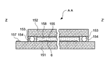
<3.液晶パネルの機械的構成>
次に、液晶パネルAAの機械的構成について図5及び図6を参照して説明する。ここで、図4は、液晶パネルAAの構成を示す斜視図であり、図6は、図5におけるZ−Z’線断面図である。
<3. Mechanical configuration of LCD panel>
Next, the mechanical configuration of the liquid crystal panel AA will be described with reference to FIGS. Here, FIG. 4 is a perspective view showing a configuration of the liquid crystal panel AA, and FIG. 6 is a sectional view taken along the line ZZ ′ in FIG.
これらの図に示されるように、液晶パネルAAは、画素電極6等が形成されたガラスや半導体等の素子基板151と、対向電極158等が形成されたガラス等の透明な対向基板152とを、スペーサ153が混入されたシール材154によって一定の間隙を保って、互いに電極形成面が対向するように貼り合わせるとともに、この間隙に電気光学材料としての液晶155を封入した構造となっている。なお、シール材154は、対向基板152の基板周辺に沿って形成されるが、液晶155を封入するために一部が開口している。このため、液晶155の封入後に、その開口部分が封止材156によって封止されている。
As shown in these figures, the liquid crystal panel AA includes an
ここで、素子基板151の対向面であって、シール材154の外側一辺においては、走査線駆動回路100が形成されて、X方向に延在するデータ線3を駆動する構成となっている。また、この一辺に隣接する一辺には、複数の入力端子157が形成され、走査線駆動回路100に駆動信号が供給されると共に、データ線3に画像信号がデータ線信号として供給される構成となっている。
Here, on the opposite surface of the
対向基板152の対向電極158は、素子基板151との貼合部分における4隅のうち、少なくとも1箇所において設けられた導通材によって、素子基板151との電気的導通が図られている。対向電極158には対向電極電位LCCOMが供給される。ほかに、対向基板152には、液晶パネルAAの用途に応じて、例えば、第1に、ストライプ状や、モザイク状、トライアングル状等に配列したカラーフィルタが設けられ、第2に、例えば、クロムやニッケルなどの金属材料や、カーボンやチタンなどをフォトレジストに分散した樹脂ブラックなどのブラックマトリクスが設けられ、第3に、液晶パネルAAに光を照射するバックライトが設けられる。特に色光変調の用途の場合には、カラーフィルタは形成されずにブラックマトリクスが対向基板152に設けられる。
The
くわえて、素子基板151および対向基板152の対向面には、それぞれ所定の方向にラビング処理された配向膜などが設けられる一方、その各背面側には配向方向に応じた偏光板(図示省略)がそれぞれ設けられる。ただし、液晶155として、高分子中に微小粒として分散させた高分子分散型液晶を用いれば、前述の配向膜、偏光板等が不要となる結果、光利用効率が高まるので、高輝度化や低消費電力化などの点において有利である。
In addition, the opposing surfaces of the
<3.応用例>
<3−1:対向電極電位LCCOMの交流化駆動>
上述した実施形態においては、対向電極電位LCCOMを一定電位として説明したが、対向電極電位LCCOMを交流化駆動してもよい。この場合、対向電極158と走査線2との間に発生する寄生容量は、駆動用電源回路30から見て負荷として作用する。走査信号Y1〜Ymは、ハイレベル(VHHXY)でアクティブとなり、ローレベル(VLLXY)で非アクティブとなる。ここで、非選択状態にある走査線2の電位を対向電極電位LCCOMの交流化駆動に同期させて変化させれば、当該走査線2の寄生容量の電荷はないので、消費電流を低減させることができる。そこで、低電圧電源VLLXYの電位を対向電極電位LCCOMに同期して変化させてもよい。この場合、低電圧電源VLLXYの電位変化幅は、対向電極電位LCCOMの電位変化幅と一致させればよい。また、走査信号Y1〜Ymがローレベルデアクティブとなる場合には、高電圧電源VHHXYの電位を対向電極電位LCCOMの交流化駆動に同期させて変化させればよい。
<3. Application example>
<3-1: AC drive of counter electrode potential LCCOM>
In the above-described embodiment, the counter electrode potential LCCOM is described as a constant potential, but the counter electrode potential LCCOM may be driven in an alternating manner. In this case, the parasitic capacitance generated between the
<3−2:電気光学装置の他の例>
また、上述した実施の形態にあっては、画素のスイッチング素子を、TFTで代表される3端子素子として説明したが、ダイオード等の2端子素子で構成しても良い。ただし、画素のスイッチング素子として2端子素子を用いる場合には、走査線2を一方の基板に形成し、データ線3を他方の基板に形成するとともに、2端子素子を、走査線2またはデータ線3のいずれか一方と、画素電極との間に形成する必要がある。この場合、画素は、走査線2とデータ線3との間に直列接続された二端子素子と、液晶とから構成されることとなる。
<3-2: Another example of electro-optical device>
Further, in the above-described embodiment, the switching element of the pixel has been described as a three-terminal element typified by a TFT, but may be configured by a two-terminal element such as a diode. However, when a two-terminal element is used as a pixel switching element, the
また、本発明は、アクティブマトリクス型液晶表示装置として説明したが、これに限られず、STN(Super Twisted Nematic)液晶などを用いたパッシブ型にも適用可能である。さらに、電気光学材料としては、液晶のほかに、エレクトロルミネッセンス素子などを用いて、その電気光学効果により表示を行う表示装置にも適用可能である。また、電気光学装置には、電子ペーパー等の電気泳動装置、電子放出素子(Field Emission Display及びSurface-Conduction Electron-Emitter Display)等を用いた装置も含まれる。
すなわち、本発明は、上述した液晶装置と類似の構成を有するすべての電気光学装置に適用可能である。
Although the present invention has been described as an active matrix liquid crystal display device, the present invention is not limited to this, and can also be applied to a passive type using STN (Super Twisted Nematic) liquid crystal. Furthermore, as an electro-optical material, in addition to liquid crystal, an electroluminescence element or the like can be used for a display device that performs display by the electro-optical effect. The electro-optical device also includes an electrophoretic device such as electronic paper, and a device using an electron-emitting device (Field Emission Display and Surface-Conduction Electron-Emitter Display).
That is, the present invention can be applied to all electro-optical devices having a configuration similar to that of the liquid crystal device described above.
<3−3:電子機器>
次に、上述した液晶表示装置を各種の電子機器に適用される場合について説明する。
<3−3−1:プロジェクタ>
まず、この液晶装置をライトバルブとして用いたプロジェクタについて説明する。図7は、プロジェクタの構成例を示す平面図である。
<3-3: Electronic equipment>
Next, the case where the above-described liquid crystal display device is applied to various electronic devices will be described.
<3-3-1: Projector>
First, a projector using this liquid crystal device as a light valve will be described. FIG. 7 is a plan view showing a configuration example of the projector.
この図に示されるように、プロジェクタ1100内部には、ハロゲンランプ等の白色光源からなるランプユニット1102が設けられている。このランプユニット1102から射出された投射光は、ライトガイド1104内に配置された4枚のミラー1106および2枚のダイクロイックミラー1108によってRGBの3原色に分離され、各原色に対応するライトバルブとしての液晶パネル1110R、1110Bおよび1110Gに入射される。
As shown in this figure, a
液晶パネル1110R、1110Bおよび1110Gの構成は、上述した液晶パネルAAと同等であり、画像信号処理回路(図示省略)から供給されるR、G、Bの原色信号でそれぞれ駆動されるものである。そして、これらの液晶パネルによって変調された光は、ダイクロイックプリズム1112に3方向から入射される。このダイクロイックプリズム1112においては、RおよびBの光が90度に屈折する一方、Gの光が直進する。したがって、各色の画像が合成される結果、投射レンズ1114を介して、スクリーン等にカラー画像が投写されることとなる。
The configuration of the
ここで、各液晶パネル1110R、1110Bおよび1110Gによる表示像について着目すると、液晶パネル1110Gによる表示像は、液晶パネル1110R、1110Bによる表示像に対して左右反転することが必要となる。
なお、液晶パネル1110R、1110Bおよび1110Gには、ダイクロイックミラー1108によって、R、G、Bの各原色に対応する光が入射するので、カラーフィルタを設ける必要はない。
Here, paying attention to the display images by the
Note that since light corresponding to the primary colors R, G, and B is incident on the
<3−5−2:モバイル型コンピュータ>
次に、この液晶パネルAAを、モバイル型のパーソナルコンピュータに適用した例について説明する。図8は、このパーソナルコンピュータの構成を示す斜視図である。図において、コンピュータ1200は、キーボード1202を備えた本体部1204と、液晶表示ユニット1206とから構成されている。この液晶表示ユニット1206は、先に述べた液晶パネル1005の背面にバックライトを付加することにより構成されている。
<3-5-2: Mobile computer>
Next, an example in which the liquid crystal panel AA is applied to a mobile personal computer will be described. FIG. 8 is a perspective view showing the configuration of this personal computer. In the figure, a
<3−5−3:携帯電話>
さらに、この液晶パネルAAを、携帯電話に適用した例について説明する。図9は、この携帯電話の構成を示す斜視図である。図において、携帯電話1300は、複数の操作ボタン1302とともに、反射型の液晶パネル1005を備えるものである。この反射型の液晶パネル1005にあっては、必要に応じてその前面にフロントライトが設けられる。
<3-5-3: Mobile phone>
Further, an example in which the liquid crystal panel AA is applied to a mobile phone will be described. FIG. 9 is a perspective view showing the configuration of this mobile phone. In the figure, a
なお、図7〜図9を参照して説明した電子機器の他にも、液晶テレビや、ビューファインダ型、モニタ直視型のビデオテープレコーダ、カーナビゲーション装置、ページャ、電子手帳、電卓、ワードプロセッサ、ワークステーション、テレビ電話、POS端末、タッチパネルを備えた装置等などが挙げられる。そして、これらの各種電子機器に適用可能なのは言うまでもない。パネル板は、電気光学材料として液晶の替わりに有機LEDを用いたもの、プラズマを用いたもの、無機エレクトロルミネッセンス素子を用いたものであってもよい。さらに、電子ペーパー等の電気泳動パネルにも適用することができる。 In addition to the electronic devices described with reference to FIGS. 7 to 9, a liquid crystal television, a viewfinder type, a monitor direct-view type video tape recorder, a car navigation device, a pager, an electronic notebook, a calculator, a word processor, a work Examples include a station, a videophone, a POS terminal, a device equipped with a touch panel, and the like. Needless to say, the present invention can be applied to these various electronic devices. The panel plate may be one using an organic LED instead of liquid crystal as an electro-optical material, one using plasma, or one using an inorganic electroluminescence element. Further, it can be applied to an electrophoretic panel such as electronic paper.
2…走査線、3…データ線、10…マイコン、30…駆動用電源、100…走査線駆動回路、200…データ線駆動回路、AA…液晶パネル、VDDXY…ロジック電源(第1電源)、VLLXY…低電圧電源(第2電源)、VHHXY…高電圧電源(第1電源)。 2 ... scanning line, 3 ... data line, 10 ... microcomputer, 30 ... drive power supply, 100 ... scan line drive circuit, 200 ... data line drive circuit, AA ... liquid crystal panel, VDDXY ... logic power supply (first power supply), VLLXY ... low voltage power supply (second power supply), VHHXY ... high voltage power supply (first power supply).
Claims (5)
第1電圧を給電する第1電源回路と、
前記第1電圧よりも高電位の第2電圧を給電する第2電源回路と、
1フレームの先頭でアクティブとなる転送開始パルスを1フレーム毎に生成するタイミング発生回路と、
前記第1電圧を給電されて前記転送開始パルスを順次シフトするシフトレジスタと、
前記第2電圧を給電されて前記シフトレジスタの出力信号のレベルを変換して前記各走査信号を出力するレベルシフタと、
前記シフトレジスタに前記第1電圧の給電を開始した後、リセット信号を供給して前記タイミング発生手段を初期化し、前記初期化後に最初の前記転送開始パルスが生成されてから少なくとも1フレーム期間が経過した後の前記転送開始パルスに基づいて前記レベルシフタへ前記第2電圧の給電を開始するように制御する制御回路と、
を備えることを特徴とする電気光学装置。 A plurality of data lines, a plurality of scanning lines, a plurality of switching elements provided corresponding to intersections of the data lines and the scanning lines, a plurality of pixel electrodes connected to the switching elements, and the scanning An electro-optical device including a scanning line driving circuit that sequentially outputs each scanning signal for driving a line,
A first power supply circuit for supplying a first voltage;
A second power supply circuit for supplying a second voltage having a higher potential than the first voltage;
A timing generation circuit that generates a transfer start pulse that becomes active at the head of one frame every frame;
A shift register that is powered by the first voltage and sequentially shifts the transfer start pulse;
A level shifter that is fed with the second voltage and converts the level of the output signal of the shift register to output each scanning signal ;
After supplying the first voltage to the shift register , a reset signal is supplied to initialize the timing generation means, and at least one frame period has elapsed since the first transfer start pulse was generated after the initialization. A control circuit that controls to start feeding the second voltage to the level shifter based on the transfer start pulse after
An electro-optical device comprising:
対向電極が形成された対向基板と、
前記素子基板と前記対向電極と間隙に電気光学材料を備え、
前記制御回路は、前記第2電圧を前記対向電極に供給するように制御する
ことを特徴とする請求項1に記載の電気光学装置。 An element substrate on which the data line, the scanning line, the switching element, and the pixel electrode are formed;
A counter substrate on which a counter electrode is formed;
An electro-optic material is provided in the gap between the element substrate and the counter electrode,
The electro-optical device according to claim 1, wherein the control circuit controls the second voltage to be supplied to the counter electrode.
前記対向電極に対して、前記第2電圧の前記高電位と前記低電位とのうち少なくとも一方を、所定周期で交互に供給することを特徴とする請求項2に記載の電気光学装置。 The second voltage includes a higher voltage and a lower voltage than the first voltage,
The electro-optical device according to claim 2, wherein at least one of the high potential and the low potential of the second voltage is alternately supplied to the counter electrode at a predetermined period.
前記第1電圧の給電を開始した後、リセット信号を供給して前記タイミング発生手段を初期化し、前記初期化後に最初の前記転送開始パルスが生成されてから少なくとも1フレーム期間が経過した後の前記転送開始パルスに基づいて前記第2電圧の給電を開始するように制御することを特徴とする電気光学装置の電源制御方法。 A plurality of data lines, a plurality of scanning lines, a plurality of switching elements provided corresponding to intersections of the data lines and the scanning lines, a plurality of pixel electrodes connected to the switching elements, and the scanning A scanning line driving circuit for sequentially outputting each scanning signal for driving the line; a first power supply circuit for supplying a first voltage; a second power supply circuit for supplying a second voltage higher than the first voltage; A timing generation circuit that generates a transfer start pulse that becomes active at the beginning of one frame every frame; a shift register that sequentially shifts the transfer start pulse in response to the first voltage; and the second voltage that receives the second voltage A power control method for an electro-optical device, comprising: a level shifter that converts a level of an output signal of a shift register and outputs each of the scanning signals,
After starting the feed of the first voltage, initializing the timing generation means to supply the reset signal, the after at least one frame period has elapsed since the beginning of the transfer start pulse is generated after the initialization A method for controlling the power supply of an electro-optical device, wherein control is performed so as to start feeding the second voltage based on a transfer start pulse .
Priority Applications (1)
| Application Number | Priority Date | Filing Date | Title |
|---|---|---|---|
| JP2003299073A JP4513289B2 (en) | 2003-08-22 | 2003-08-22 | ELECTRO-OPTICAL DEVICE, ELECTRONIC DEVICE, AND POWER CONTROL METHOD FOR ELECTRO-OPTICAL DEVICE |
Applications Claiming Priority (1)
| Application Number | Priority Date | Filing Date | Title |
|---|---|---|---|
| JP2003299073A JP4513289B2 (en) | 2003-08-22 | 2003-08-22 | ELECTRO-OPTICAL DEVICE, ELECTRONIC DEVICE, AND POWER CONTROL METHOD FOR ELECTRO-OPTICAL DEVICE |
Publications (2)
| Publication Number | Publication Date |
|---|---|
| JP2005070337A JP2005070337A (en) | 2005-03-17 |
| JP4513289B2 true JP4513289B2 (en) | 2010-07-28 |
Family
ID=34404391
Family Applications (1)
| Application Number | Title | Priority Date | Filing Date |
|---|---|---|---|
| JP2003299073A Expired - Fee Related JP4513289B2 (en) | 2003-08-22 | 2003-08-22 | ELECTRO-OPTICAL DEVICE, ELECTRONIC DEVICE, AND POWER CONTROL METHOD FOR ELECTRO-OPTICAL DEVICE |
Country Status (1)
| Country | Link |
|---|---|
| JP (1) | JP4513289B2 (en) |
Families Citing this family (4)
| Publication number | Priority date | Publication date | Assignee | Title |
|---|---|---|---|---|
| JP5047662B2 (en) * | 2007-03-28 | 2012-10-10 | 株式会社ジャパンディスプレイイースト | Display device |
| US8248341B2 (en) * | 2009-04-15 | 2012-08-21 | Store Electronic Systems Sa | Low power active matrix display |
| KR101962603B1 (en) | 2009-10-16 | 2019-03-28 | 가부시키가이샤 한도오따이 에네루기 켄큐쇼 | Liquid crystal display device and electronic device including the liquid crystal display device |
| KR101648571B1 (en) * | 2014-07-16 | 2016-08-18 | 엘지디스플레이 주식회사 | In-cell touch type display device |
Citations (5)
| Publication number | Priority date | Publication date | Assignee | Title |
|---|---|---|---|---|
| JPH09171166A (en) * | 1995-12-19 | 1997-06-30 | Sanyo Electric Co Ltd | Liquid crystal display device |
| JP2000105566A (en) * | 1998-07-29 | 2000-04-11 | Casio Comput Co Ltd | Display driving integrated circuit |
| JP2000305504A (en) * | 1999-02-18 | 2000-11-02 | Sony Corp | Power generation circuit and generation method thereof and liquid crystal display device |
| JP2003114653A (en) * | 2001-10-03 | 2003-04-18 | Casio Comput Co Ltd | Display driving device |
| JP2003216117A (en) * | 2002-01-23 | 2003-07-30 | Matsushita Electric Ind Co Ltd | Method for driving liquid crystal display |
-
2003
- 2003-08-22 JP JP2003299073A patent/JP4513289B2/en not_active Expired - Fee Related
Patent Citations (5)
| Publication number | Priority date | Publication date | Assignee | Title |
|---|---|---|---|---|
| JPH09171166A (en) * | 1995-12-19 | 1997-06-30 | Sanyo Electric Co Ltd | Liquid crystal display device |
| JP2000105566A (en) * | 1998-07-29 | 2000-04-11 | Casio Comput Co Ltd | Display driving integrated circuit |
| JP2000305504A (en) * | 1999-02-18 | 2000-11-02 | Sony Corp | Power generation circuit and generation method thereof and liquid crystal display device |
| JP2003114653A (en) * | 2001-10-03 | 2003-04-18 | Casio Comput Co Ltd | Display driving device |
| JP2003216117A (en) * | 2002-01-23 | 2003-07-30 | Matsushita Electric Ind Co Ltd | Method for driving liquid crystal display |
Also Published As
| Publication number | Publication date |
|---|---|
| JP2005070337A (en) | 2005-03-17 |
Similar Documents
| Publication | Publication Date | Title |
|---|---|---|
| JP4123711B2 (en) | Electro-optical panel driving method, electro-optical device, and electronic apparatus | |
| US7023415B2 (en) | Shift register, data-line driving circuit, and scan-line driving circuit | |
| JP4985020B2 (en) | Liquid crystal device, driving method thereof, and electronic apparatus | |
| KR100840311B1 (en) | Liquid Crystal Display and Driving Method thereof | |
| US6781565B2 (en) | Electro-optical device, driving circuit and driving method of electro-optical device, and electronic apparatus | |
| JP3873003B2 (en) | Liquid crystal display device and TFT substrate | |
| KR100429944B1 (en) | Driving method for electro-optical panel, driving circuit for data lines thereof, electro-optical apparatus, and electronic equipment | |
| JP4111174B2 (en) | Electro-optical panel, electro-optical device and electronic apparatus | |
| JP2003308050A (en) | Drive circuit and electro-optical panel | |
| CN101630476A (en) | Driver and method for driving electro-optical device, electro-optical device, and electronic apparatus | |
| JP3692846B2 (en) | Shift register, shift register control method, data line driving circuit, scanning line driving circuit, electro-optical panel, and electronic apparatus | |
| US7095405B2 (en) | Output control circuit, driving circuit, electro-optic apparatus, and electronic instrument | |
| JP4513289B2 (en) | ELECTRO-OPTICAL DEVICE, ELECTRONIC DEVICE, AND POWER CONTROL METHOD FOR ELECTRO-OPTICAL DEVICE | |
| JP4483224B2 (en) | Electro-optical panel, electro-optical device, and electronic apparatus | |
| JP4461687B2 (en) | Electro-optical panel, driving circuit and driving method thereof, and electronic apparatus | |
| JP3997727B2 (en) | Electro-optic panel and electronic equipment | |
| KR100783704B1 (en) | Liquid Crystal Display and driving apparatus and method thereof | |
| JP4449366B2 (en) | Electro-optical device and electronic apparatus | |
| KR100656916B1 (en) | Liquid crystal display, drive device and method thereof for increasing initial bend orientation | |
| JP4419394B2 (en) | Electro-optical panel driving method and driving circuit, electro-optical panel using the same, and electronic apparatus | |
| JP4254427B2 (en) | Electro-optical device and electronic apparatus | |
| JP3837998B2 (en) | Level conversion circuit, data line driving circuit, electro-optical device, and electronic apparatus | |
| JP2008033362A (en) | Electro-optical panel driving method, electro-optical device, and electronic apparatus | |
| JP4111212B2 (en) | Drive circuit, electro-optical device, and electronic device | |
| JP3998038B2 (en) | Electro-optical device, scanning line driving circuit, driving method, and electronic apparatus |
Legal Events
| Date | Code | Title | Description |
|---|---|---|---|
| A621 | Written request for application examination |
Free format text: JAPANESE INTERMEDIATE CODE: A621 Effective date: 20060726 |
|
| RD04 | Notification of resignation of power of attorney |
Free format text: JAPANESE INTERMEDIATE CODE: A7424 Effective date: 20070403 |
|
| A977 | Report on retrieval |
Free format text: JAPANESE INTERMEDIATE CODE: A971007 Effective date: 20090930 |
|
| A131 | Notification of reasons for refusal |
Free format text: JAPANESE INTERMEDIATE CODE: A131 Effective date: 20091013 |
|
| A521 | Written amendment |
Free format text: JAPANESE INTERMEDIATE CODE: A523 Effective date: 20091210 |
|
| A131 | Notification of reasons for refusal |
Free format text: JAPANESE INTERMEDIATE CODE: A131 Effective date: 20100202 |
|
| A521 | Written amendment |
Free format text: JAPANESE INTERMEDIATE CODE: A523 Effective date: 20100401 |
|
| TRDD | Decision of grant or rejection written | ||
| A01 | Written decision to grant a patent or to grant a registration (utility model) |
Free format text: JAPANESE INTERMEDIATE CODE: A01 Effective date: 20100420 |
|
| A01 | Written decision to grant a patent or to grant a registration (utility model) |
Free format text: JAPANESE INTERMEDIATE CODE: A01 |
|
| A61 | First payment of annual fees (during grant procedure) |
Free format text: JAPANESE INTERMEDIATE CODE: A61 Effective date: 20100503 |
|
| R150 | Certificate of patent or registration of utility model |
Free format text: JAPANESE INTERMEDIATE CODE: R150 |
|
| FPAY | Renewal fee payment (event date is renewal date of database) |
Free format text: PAYMENT UNTIL: 20130521 Year of fee payment: 3 |
|
| FPAY | Renewal fee payment (event date is renewal date of database) |
Free format text: PAYMENT UNTIL: 20140521 Year of fee payment: 4 |
|
| S531 | Written request for registration of change of domicile |
Free format text: JAPANESE INTERMEDIATE CODE: R313531 |
|
| R350 | Written notification of registration of transfer |
Free format text: JAPANESE INTERMEDIATE CODE: R350 |
|
| LAPS | Cancellation because of no payment of annual fees |