JP4508253B2 - Three-dimensional structure and manufacturing method thereof - Google Patents
Three-dimensional structure and manufacturing method thereof Download PDFInfo
- Publication number
- JP4508253B2 JP4508253B2 JP2008064359A JP2008064359A JP4508253B2 JP 4508253 B2 JP4508253 B2 JP 4508253B2 JP 2008064359 A JP2008064359 A JP 2008064359A JP 2008064359 A JP2008064359 A JP 2008064359A JP 4508253 B2 JP4508253 B2 JP 4508253B2
- Authority
- JP
- Japan
- Prior art keywords
- dimensional structure
- elastic body
- cantilever
- substrate member
- fixed
- Prior art date
- Legal status (The legal status is an assumption and is not a legal conclusion. Google has not performed a legal analysis and makes no representation as to the accuracy of the status listed.)
- Expired - Fee Related
Links
Images


Classifications
-
- G—PHYSICS
- G01—MEASURING; TESTING
- G01L—MEASURING FORCE, STRESS, TORQUE, WORK, MECHANICAL POWER, MECHANICAL EFFICIENCY, OR FLUID PRESSURE
- G01L5/00—Apparatus for, or methods of, measuring force, work, mechanical power, or torque, specially adapted for specific purposes
- G01L5/22—Apparatus for, or methods of, measuring force, work, mechanical power, or torque, specially adapted for specific purposes for measuring the force applied to control members, e.g. control members of vehicles, triggers
- G01L5/226—Apparatus for, or methods of, measuring force, work, mechanical power, or torque, specially adapted for specific purposes for measuring the force applied to control members, e.g. control members of vehicles, triggers to manipulators, e.g. the force due to gripping
- G01L5/228—Apparatus for, or methods of, measuring force, work, mechanical power, or torque, specially adapted for specific purposes for measuring the force applied to control members, e.g. control members of vehicles, triggers to manipulators, e.g. the force due to gripping using tactile array force sensors
-
- B—PERFORMING OPERATIONS; TRANSPORTING
- B81—MICROSTRUCTURAL TECHNOLOGY
- B81B—MICROSTRUCTURAL DEVICES OR SYSTEMS, e.g. MICROMECHANICAL DEVICES
- B81B7/00—Microstructural systems; Auxiliary parts of microstructural devices or systems
- B81B7/04—Networks or arrays of similar microstructural devices
-
- G—PHYSICS
- G01—MEASURING; TESTING
- G01L—MEASURING FORCE, STRESS, TORQUE, WORK, MECHANICAL POWER, MECHANICAL EFFICIENCY, OR FLUID PRESSURE
- G01L5/00—Apparatus for, or methods of, measuring force, work, mechanical power, or torque, specially adapted for specific purposes
- G01L5/16—Apparatus for, or methods of, measuring force, work, mechanical power, or torque, specially adapted for specific purposes for measuring several components of force
- G01L5/161—Apparatus for, or methods of, measuring force, work, mechanical power, or torque, specially adapted for specific purposes for measuring several components of force using variations in ohmic resistance
- G01L5/162—Apparatus for, or methods of, measuring force, work, mechanical power, or torque, specially adapted for specific purposes for measuring several components of force using variations in ohmic resistance of piezoresistors
-
- B—PERFORMING OPERATIONS; TRANSPORTING
- B81—MICROSTRUCTURAL TECHNOLOGY
- B81B—MICROSTRUCTURAL DEVICES OR SYSTEMS, e.g. MICROMECHANICAL DEVICES
- B81B2201/00—Specific applications of microelectromechanical systems
- B81B2201/02—Sensors
- B81B2201/0292—Sensors not provided for in B81B2201/0207 - B81B2201/0285
Landscapes
- Physics & Mathematics (AREA)
- General Physics & Mathematics (AREA)
- Engineering & Computer Science (AREA)
- Computer Hardware Design (AREA)
- Microelectronics & Electronic Packaging (AREA)
- Chemical & Material Sciences (AREA)
- Analytical Chemistry (AREA)
- Force Measurement Appropriate To Specific Purposes (AREA)
- Micromachines (AREA)
- Pressure Sensors (AREA)
Description
本発明は、MEMS(Micro Electro Mechanical Systems)技術あるいはNEMS(Nano Electro Mechanical Systems)技術を用いて3次元的に形成された構造体およびその製造方法に関し、特に、可動構造を有する微小3次元構造体要素が弾性体内へ配置された素子と、この素子を用いて構成された3次元構造体、ならびにそれらの製造方法に関する。 The present invention relates to a structure formed three-dimensionally using MEMS (Micro Electro Mechanical Systems) technology or NEMS (Nano Electro Mechanical Systems) technology, and a method for manufacturing the same, and in particular, a micro three-dimensional structure having a movable structure. The present invention relates to an element in which an element is arranged in an elastic body, a three-dimensional structure formed using the element, and a method for manufacturing the same.
ロボット技術の研究、開発においては、ロボットハンドにより対象物を如何にして確実に制御するのかということが、重要な課題の一つとなっている。具体的には、ロボットハンドにより対象物を掴むという動作に着目すれば、対象物を掴む握力を検出するだけでなく、この掴むという動作によりハンド表面に生じるせん断応力をも検出することが、ロボットハンドの確実な制御のためには必要となる。これは、対象物とハンド表面との間に生じる摩擦力をこのせん断応力により検出することで、最適な摩擦力の制御を行って対象物の確実な制御を実現することに役立つからである。 In the research and development of robot technology, one of the important issues is how to reliably control an object with a robot hand. Specifically, if attention is paid to the action of grasping the object by the robot hand, the robot can detect not only the gripping force for grasping the object but also the shear stress generated on the surface of the hand by the action of grasping. This is necessary for reliable control of the hand. This is because the frictional force generated between the object and the surface of the hand is detected by the shear stress, so that the optimum frictional force control can be performed to realize the reliable control of the object.
近年、このようなせん断応力を検出することを目的とした触覚センサが開発されつつある(例えば、特許文献1参照)。このような従来の触覚センサの一例について、図8に示す模式斜視図を用いて以下に説明する。 In recent years, tactile sensors aimed at detecting such shear stress have been developed (for example, see Patent Document 1). An example of such a conventional tactile sensor will be described below with reference to a schematic perspective view shown in FIG.
図8に示すように、触覚センサ501は、数百nm程度の薄膜で形成された複数のピエゾ抵抗カンチレバー502(そのヒンジ部にピエゾ抵抗体を備えたカンチレバー)が、互いに独立して膜状弾性体503内に配置された構成を有している。
As shown in FIG. 8, the
このカンチレバー502は、その一端が固定部として形成され、その他端がカンチレバー502を形成する薄膜の厚み方向にのみ変形可能な可動部として形成されている。各々のカンチレバー502は、図示しない端子部および配線を通して、図示しない制御装置に電気的に接続されている。例えば、膜状弾性体503表面にせん断力あるいは圧力が付加された場合、膜状弾性体503内部に生じたせん断応力あるいは圧縮応力がカンチレバー502の可動部を動作させて変形させることで、このせん断力あるいは圧力を検出することが可能となっている。また、膜状弾性体503に作用する様々な方向のせん断応力あるいは圧縮応力を検出するために、それぞれのカンチレバー502は、可動部の変形方向が異なるように、例えば、図示X軸方向、Y軸方向、及びZ軸方向のそれぞれの方向にその変形方向が配置されるように、膜状弾性体503内に配置されている。
One end of the
このように触覚センサ501が構成されていることにより、膜状弾性体503が対象物等に接触することにより、膜状弾性体503内に生じる様々な向きのせん断応力あるいは圧縮応力を、それぞれのカンチレバー502により検出することが可能となっている。なお、このような膜状弾性体503は、外力付加により容易に弾性変形するような材料として、例えばPDMS(Polydimethylsiloxane)により形成されている。
Since the
次に、このような構成を有する触覚センサ501の製造方法について説明する。
図9の模式説明図に示すように、例えば、2個のカンチレバー502が形成されたSOIウェハ510を、PDMSにて形成されたスペーサ516にて支持させた状態で容器517内に配置する。その後、図9に示すように、容器517内に流動状態の弾性体PDMS519を注入する。このPDMS519の注入は、少なくともそれぞれのカンチレバー502及びSOIウェハ510へのカンチレバー502の固定部分が、注入されたPDMS519内に浸積されて埋設されるように行われる。
Next, a manufacturing method of the
As shown in the schematic explanatory view of FIG. 9, for example, an
その後、容器517内に注入されたPDMS519が硬化した後、PDMS519より露出された状態にあるSOIウェハ510の表面に付着している強度補強部材であるパリレン層518の部分的な除去を、例えばO2プラズマエッチングにより行う。
Thereafter, after the
次に、容器517の上面よりエッチング処理を施すことで、PDMS519より露出された状態にあるSOIウェハ510の犠牲層であるSi511およびSiO2層512を除去する。その結果、図10に示すように、それぞれのカンチレバー502のSOIウェハ510への固定部分が除去されて、PDMS519の表面においてそれぞれの凹部520が形成された状態となる。従って、それぞれのカンチレバー2を固定していた犠牲層が除去されることで、PDMS519内において、個々のカンチレバー502が互いに独立して配置された状態とされる。
Next, an etching process is performed from the upper surface of the
その後、図11に示すように、PDMS519の表面に形成されたそれぞれの凹部520内に流動状態のPDMS519を注入して、PDMS519の補充を行う。この補充の後、注入されたPDMS519を硬化させることによりPDMSにより形成された膜状弾性体503が形成され、触覚センサ501が完成する。
After that, as shown in FIG. 11, PDMS 519 in a fluid state is injected into each
このような構造を有する触覚センサ501では、SOIウェハ510上に形成されたカンチレバー502を、PDMS519内に配置した後、SOIウェハ510への固定部分である犠牲層の除去を行うという製造方法が採用されているため、SOIウェハ510におけるそれぞれのカンチレバー502の形成位置が、そのまま触覚センサ501におけるそれぞれのカンチレバー502の形成位置となる。そのため、例えば、大面積のシート状の膜状弾性体503内を用いた触覚センサ501を形成することが困難であるという問題がある。また、SOIウェハ510におけるカンチレバー502の形成位置に限定されることから、所望のピッチでカンチレバー502を膜状弾性体503内に配置することも困難となる。すなわち、触覚センサ501の大きさやカンチレバー502の配置間隔が制約され、その用途に応じた仕様の触覚センサ501を製造することができないという問題がある。
The
仮に、例えば、多数のカンチレバー502が形成されたSOIウェハ510を切断して、それぞれのカンチレバー502を個片化するような場合には、微小な構造体であるカンチレバー502に破損等が生じる恐れもあり、その取り扱いが困難となることが考えられる。
For example, when the SOI wafer 510 on which a large number of
従って、本発明の目的は、上記問題を解決することにあって、MEMS技術あるいはNEMS技術を用いて形成された可動構造を有する微小3次元構造体要素が膜状弾性体内へ配置された3次元構造体において、所望の位置に微小3次元構造体要素を配置することで様々な仕様に対応することができるとともに、その製造における取り扱い性を良好なものとすることができる3次元構造体構成用素子および3次元構造体、ならびにそれらの製造方法を提供することにある。 Accordingly, an object of the present invention is to solve the above-described problem, and a three-dimensional structure in which a micro three-dimensional structure element having a movable structure formed by using a MEMS technique or a NEMS technique is arranged in a film-like elastic body. For a three-dimensional structure structure that can meet various specifications by arranging a minute three-dimensional structure element at a desired position in the structure, and that can be easily handled in its manufacture. An object is to provide an element, a three-dimensional structure, and a method of manufacturing the same.
上記目的を達成するために、本発明は以下のように構成する。 In order to achieve the above object, the present invention is configured as follows.
本発明の第1態様によれば、複数の貫通開口部が形成された基板部材と、
上記貫通開口部のそれぞれの縁部に固定される固定部を有する可動構造に形成された微小3次元構造体要素と、
上記複数の貫通開口部及び上記微小3次元構造体要素全体を覆う弾性体とを備え、
上記基板部材における上記貫通開口部のそれぞれの周囲近傍に複数の係合用孔部が形成され、上記複数の係合用孔部内に上記弾性体が充填されて、上記弾性体が上記基板部材に固定されている、3次元構造体構成用素子を提供する。
According to the first aspect of the present invention, a substrate member in which a plurality of through openings are formed;
A micro three-dimensional structure element formed in a movable structure having a fixed portion fixed to each edge of the through opening ;
An elastic body covering the plurality of through openings and the entire micro three-dimensional structure element ;
A plurality of engaging holes are formed in the vicinity of each of the through openings in the substrate member, the elastic bodies are filled in the plurality of engaging holes, and the elastic body is fixed to the substrate member. The three-dimensional structure constituting element is provided.
本発明の第2態様によれば、上記可動構造は、実質的に一の方向に変形可能な構造であって、
互いに変形可能な方向が異なる複数の上記微小3次元構造体要素が、1つの上記基板部材に固定された状態にて、1つの上記弾性体により覆われている、第1態様に記載の3次元構造体構成用素子を提供する。
According to a second aspect of the present invention, the movable structure is a structure that is substantially deformable in one direction,
The three-dimensional structure according to the first aspect, wherein a plurality of the minute three-dimensional structure elements having different deformable directions are covered with one elastic body in a state of being fixed to one substrate member. An element for constructing a structure is provided.
本発明の第3態様によれば、上記基板部材は、それぞれの上記微小3次元構造体要素との間で電気信号の受け渡しを行う共通の回路部を有する、第2態様に記載の3次元構造体構成用素子を提供する。
According to a third aspect of the present invention, the substrate member has a common circuit section for transferring an electric signal to and from each of the minute three-dimensional structure elements, and the three-dimensional structure according to the second aspect. A body constituting element is provided.
本発明の第4態様によれば、第1態様から第3態様のいずれか1つに記載の複数の3次元構造体構成用素子と、
上記複数の3次元構造体構成用素子を、互いの上記基板部材を離間させた状態にてその内部に配置する膜状弾性体とを備える、3次元構造体を提供する。
According to a fourth aspect of the present invention, the plurality of three-dimensional structure constituting elements according to any one of the first aspect to the third aspect ;
Provided is a three-dimensional structure including a plurality of three-dimensional structure constructing elements and a film-like elastic body arranged inside the substrate members in a state where the substrate members are separated from each other.
本発明の第5態様によれば、上記弾性体を形成する樹脂は、上記膜状弾性体を形成する樹脂よりも、その溶融状態にて高い流動性を有する、第4態様に記載の3次元構造体を提供する。
According to the fifth aspect of the present invention, the resin forming the elastic body has higher fluidity in its molten state than the resin forming the film-like elastic body, and the three-dimensional according to the fourth aspect. Provide a structure.
本発明の第6態様によれば、上記複数の3次元構造体構成素子が実装されたフレキシブル基板をさらに備え、
上記フレキシブル基板は、上記膜状弾性体の内部に配置されている、第4態様または第5態様に記載の3次元構造体を提供する。
According to the sixth aspect of the present invention, it further comprises a flexible substrate on which the plurality of three-dimensional structure constituting elements are mounted,
The said flexible substrate provides the three-dimensional structure as described in a 4th aspect or a 5th aspect arrange | positioned inside the said film-like elastic body.
本発明の第7態様によれば、可動構造を有する複数の微小3次元構造体要素の固定部が基板部材において固定される位置である固定位置の周囲近傍に、複数の係合用孔部を形成した後、
上記固定部がそれぞれの縁部に形成された複数の貫通開口部を上記基板部材に形成した後、
流動状態の樹脂材料を上記基板部材上に供給して、上記樹脂材料によって上記複数の貫通開口部及び上記微小3次元構造体要素を覆うとともに、上記複数の係合用孔部内に上記樹脂材料を充填させ、
その後、上記樹脂材料を硬化させることにより、上記樹脂材料により形成された上記弾性体を上記基板部材に固定し、
その後、上記基板部材と上記弾性体を切断して、上記複数の微小3次元構造体要素を分割して、分割された上記基板部材に1又は複数の上記微小3次元構造体要素が固定され、かつ分割された上記弾性体内に配置された複数の3次元構造体構成用素子を形成する、3次元構造体構成用素子の製造方法を提供する。
According to the seventh aspect of the present invention, the plurality of engagement hole portions are formed in the vicinity of the periphery of the fixed position where the fixed portions of the plurality of minute three-dimensional structure elements having the movable structure are fixed on the substrate member . After
After forming a plurality of through openings formed in the respective edge portions of the fixing portion in the substrate member,
A resin material in a fluid state is supplied onto the substrate member, the plurality of through openings and the micro three-dimensional structure element are covered with the resin material, and the resin material is filled in the plurality of engagement holes. Let
Thereafter, by curing the resin material, the elastic body formed of the resin material is fixed to the substrate member,
Thereafter, the substrate member and the elastic body are cut to divide the plurality of minute three-dimensional structure elements, and one or more minute three-dimensional structure elements are fixed to the divided substrate member, Also provided is a method for manufacturing a three-dimensional structure constituting element which forms a plurality of three-dimensional structure constituting elements arranged in the divided elastic body.
本発明の第8態様によれば、第7態様の製造方法により製造された上記複数の3次元構造体構成用素子を、互いに上記基板部材を離間させた状態にて膜状弾性体の内部に配置して3次元構造体を形成する、3次元構造体の製造方法を提供する。
According to the eighth aspect of the present invention, the plurality of three-dimensional structure constituting elements manufactured by the manufacturing method of the seventh aspect are placed inside the film-like elastic body in a state where the substrate members are separated from each other. Provided is a method for manufacturing a three-dimensional structure, which is arranged to form a three-dimensional structure.
本発明の第9態様によれば、上記弾性体を形成する樹脂は、上記膜状弾性体を形成する樹脂よりも、その溶融状態にて高い流動性を有する、第8態様に記載の3次元構造体の製造方法を提供する。
According to the ninth aspect of the present invention, the resin forming the elastic body has a higher fluidity in its molten state than the resin forming the film-like elastic body, according to the eighth aspect. A method for manufacturing a structure is provided.
本発明によれば、基板部材に固定された微小3次元構造体要素を覆うようにその内部に配置するとともに、基板部材に固定された弾性体を有する複数の3次元構造体構成用素子が、互いの基板部材を離間させて状態にて膜状弾性体内に配置させて3次元構造体を構成する。そのため、膜状弾性体内にて、複数の3次元構造体構成用素子を、所望の配置間隔や位置に配置することができ、様々な仕様に対応することができる3次元構造体を提供することができる。 According to the present invention, a plurality of three-dimensional structure constructing elements that are disposed inside the micro three-dimensional structure element fixed to the substrate member and have an elastic body fixed to the substrate member, A three-dimensional structure is formed by arranging the substrate members in a film-like elastic body in a state of being separated from each other. Therefore, it is possible to arrange a plurality of three-dimensional structure constituting elements in a film-like elastic body at desired arrangement intervals and positions, and to provide a three-dimensional structure that can correspond to various specifications. Can do.
また、本発明の3次元構造体構成用素子の製造方法によれば、基板部材上に形成された複数の微小3次元構造体要素を弾性体にて覆った後、基板部材と弾性体とを切断することで、1又は複数の微小3次元構造体要素を分割して、複数の3次元構造体構成用素子を形成することができる。この切断処理を行う際に、それぞれの微小3次元構造体要素は、弾性体により覆われて保護されているため、微小3次元構造体要素の損傷を防止することができるとともに、分割して形成された3次元構造体構成用素子の取り扱い性を良好なものとすることができる。 Moreover, according to the method for manufacturing a three-dimensional structure constituting element of the present invention, after covering a plurality of minute three-dimensional structure elements formed on the substrate member with an elastic body, the substrate member and the elastic body are bonded together. By cutting, one or a plurality of minute three-dimensional structure elements can be divided to form a plurality of three-dimensional structure constituting elements. When performing this cutting process, each micro three-dimensional structure element is covered and protected by an elastic body, so that the micro three-dimensional structure element can be prevented from being damaged and divided. The handleability of the formed three-dimensional structure constituting element can be improved.
また、基板部材に設けられた係合部と弾性体とが係合されることで、基板部材への弾性体の固定が行われていることにより、この固定における強度を高めることができる。したがって、3次元構造体構成用素子において、微小3次元構造体要素の可動構造と弾性体との一体性を高めることができ、可動構造の動作と弾性体の変形との関連性を強めることができる。 In addition, since the elastic body is fixed to the board member by engaging the engaging portion provided on the board member and the elastic body, the strength in this fixing can be increased. Therefore, in the element for constituting a three-dimensional structure, the unity between the movable structure of the minute three-dimensional structure element and the elastic body can be enhanced, and the relationship between the operation of the movable structure and the deformation of the elastic body can be strengthened. it can.
以下に、本発明にかかる実施の形態を図面に基づいて詳細に説明する。 Embodiments according to the present invention will be described below in detail with reference to the drawings.
本発明の一の実施形態にかかる3次元構造体の一例である触覚センサ(あるいは触覚センサ構造体)を構成するために用いられる3次元構造体構成用素子の一例であるセンサ素子1の模式的な構造を示す模式斜視図を図1に示す。
1 is a schematic diagram of a
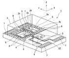
図1に示すように、本実施形態のセンサ素子1は、可動構造を有する微小3次元構造体要素の一例である複数のカンチレバー2と、複数のカンチレバー2が固定された基板部材4と、それぞれのカンチレバー2全体を覆うように基板部材4上に固定された弾性体3とを備えている。
As shown in FIG. 1, the
センサ素子1の模式説明図である図2に示すように、それぞれのカンチレバー2は、例えば数百nm程度の厚さにて薄膜状に形成されており、その一端(固定端)を固定部2bとして基板部材4に固定され、その他端(自由端)を可動部2aとして、可動構造、すなわち片持ち梁構造にて形成されている。カンチレバー2は、その幅方向に対して厚み寸法が十分に薄くなるように形成されており、固定部2bに対して可動部2aを厚み方向に変形可能となっている。さらに、それぞれのカンチレバー2は、可動部2aと固定部2bとを接続し、その変形により可動部2aが動作するような接続部の一例であるヒンジ部2cが設けられており、このヒンジ部2cには、可動部2aの動作角度を電気的に検出するためのピエゾ抵抗部が設けられている。
As shown in FIG. 2 which is a schematic explanatory view of the
また、図1に示すように、センサ素子1には、その可動部2aの変形の方向が異なる3種類のカンチレバー2が備えられており、例えば、図示X軸方向をその変形の方向とするX軸方向用カンチレバー2Xと、図示Y軸方向をその変形の方向とするY軸方向用カンチレバー2Yと、図示Z軸方向をその変形の方向とするZ軸方向用カンチレバー2Zとが備えられている。なお、図1において、X軸方向とY軸方向は、基板部材4の表面沿いにおいて互いに直交する方向であり、さらにX軸方向及びY軸方向に直交する方向がZ軸方向となっている。
As shown in FIG. 1, the
また、弾性体3は、外力の付加等により弾性変形し、その弾性変形がカンチレバー2の可動部2aを動作(変形)させるような柔軟性を有する弾性材料により形成されており、このような弾性材料としては、例えば透明又は着色されたPDMS(Polydimethylsiloxane)が用いられる。また、弾性体3は、それぞれのカンチレバー2が直接的に外部の物体等と接触して損傷を受けることが無いように保護する機能も有しており、それぞれのカンチレバー2全体を覆うような厚み寸法、例えば300μm〜1mm以下程度の厚さ寸法に形成されており、後述するカンチレバー2の応力検出機能を効果的に達成しながら、柔軟性と強度とを両立することができるような厚さ寸法に形成されていることがより望ましい。
The
また、図1に示すように、基板部材4におけるそれぞれのカンチレバー2の形成位置には、カンチレバー2毎に貫通開口部5が形成されており、この貫通開口部5の縁部にカンチレバー2の固定部2bが固定されている。また、それぞれの貫通開口部5の縁部にカンチレバー2の可動部2aが干渉することがない大きさに貫通開口部5が形成されている。
Further, as shown in FIG. 1, a through
さらに、図1においては図示しないが、それぞれのカンチレバー2における固定部2bには端子部が設けられており、これらの端子部には配線6が個別に設けられて、各々のカンチレバー2における可動部2aの動作角度を電気的に検出することが可能となっている。また、センサ素子1には、それぞれのカンチレバー2との間で配線6を通して電気信号の受け渡しを行う回路部(制御回路等、図示しない)が設けられている。
Further, although not shown in FIG. 1, terminal portions are provided in the fixed
また、基板部材4の図示Y軸方向の両端部には、それぞれの配線6が接続された電極端子7が設けられている。基板部材4の上面においては、それぞれの電極端子7を露出させ、かつそれぞれの貫通開口部5およびカンチレバー2全体を完全に覆うように、弾性体3が配置されている。図1においては電極端子7が基板部材4の上面に露出しているが、電極端子7は基板部材4の裏面に露出していても良い。この場合は基板部材4を貫通する導電体等により、電極端子7は配線6と電気的に接続される。
Further,
さらに、図1に示すように、それぞれの貫通開口部5の周囲における基板部材4の上面には、係合部の一例である多数の係合用孔部8が形成されている。この係合用孔部8内には、弾性体3が充填されており、それぞれの係合用孔部8とその内側に充填された弾性体3との係合により、弾性体3と基板部材4とが強固に係合されて固定された状態とされている。このような係合用孔部8内へ確実に弾性体3を充填させるために、弾性体3として、例えばナノスケールの構造体(孔部等)内にも入り込みやすいという高い流動性(硬化前の溶融状態にて)を有する材料を用いることが好ましい。このような材料としては、例えば、ナノスケールの構造体の型取り・転写などに利用されるDowCorning社製のSylgard184という製品を用いることができる。
Further, as shown in FIG. 1, a large number of
このような構成を有するセンサ素子1においては、弾性体3に外力が付加されることにより、その内部に生じるせん断応力または圧縮応力を、その応力が生じる方向をその変形方向とする可動部2aを有するカンチレバー2の可動部2aが動作変形されることでもって検出することが可能となっている。なお、図1におけるX軸方向用カンチレバー2XとY軸方向用カンチレバー2Yは、膜状弾性体3の表面沿いの方向に生じる力(せん断力)を検出するせん断力センサとして機能し、Z軸方向用カンチレバー2Zは、膜状弾性体3のZ軸方向の力、すなわち圧縮応力を検出する圧力センサとして機能する。なお、Z軸方向用カンチレバー2Zは、図1に示すように、カンチレバー2Xおよび2Yと同様に、片持ち梁形状に形成されるような場合であってもよく、あるいはこのような場合に代えて、その両端が基板部材4に固定されるような両持ち梁形状に形成されるような場合であってもよい。
In the
ここで、このようなカンチレバー2により応力を検出する原理について、図2に示すセンサ素子1の模式説明図を用いて説明する。
Here, the principle of detecting the stress by the
図2に示すように、センサ素子1において、弾性体3の表面に沿った外力が作用されると、弾性体3において水平方向にせん断応力τが生じ、弾性体3が弾性的に変形されて、水平方向にせん断歪みγが生じることになる。弾性体3内に配置されているカンチレバー2は、その可動部2aが弾性体3と一体的に歪むこととなり、その結果、せん断歪みγだけその変形方向(例えば図示X軸方向)に変形される、すなわち弾性的に変形されることとなる。
As shown in FIG. 2, when an external force along the surface of the
一方、カンチレバー2のヒンジ部2cには、ピエゾ抵抗部が設けられている。このピエゾ抵抗部は、可動部2aの変形量に応じてその電気的な抵抗値が変化するという機能を有しているとともに、このような変形量と抵抗値の相関性が予め測定されて、電極端子7と接続される図示しない制御装置等に相関性データとして入力保持されている。従って、このせん断応力τにより弾性体3に生じたせん断歪みγがカンチレバー2を変形させた量に基づくピエゾ抵抗部の抵抗変化を検出することで、外力作用により弾性体3に生じるせん断応力τを検出することができる。なお、このような可動部2aの変形量検出による応力検出の原理によれば、弾性体3の表面沿いの方向の力を検出するX軸方向用カンチレバー2X及びY軸方向用カンチレバー2Yにおける可動部の起き上がり角度は、90度に設定されることが好ましく、圧力を検出するZ軸方向用カンチレバー2Zにおける可動部の起き上がり角度は、0度に設定されることが好ましい。
On the other hand, the
次に、このような構造を有する複数のセンサ素子1が用いられた触覚センサ10の構造について、図3の模式図を用いて説明する。
Next, the structure of the
図3に示すように、触覚センサ10は、複数のセンサ素子1が、所定の位置に実装されたフレキシブル基板11と、これらのセンサ素子1およびフレキシブル基板11全体を覆うように、その内部に配置する膜状弾性体12とを備えている。フレキシブル基板11は、高い柔軟性を有しており、実装されたそれぞれのセンサ素子との間で信号の伝送を行う配線13が形成されている。なお、この配線13は、センサ素子1の基板部材4の上面に露出している電極端子7に導電体のワイヤを介して接続されている、またはセンサ素子1の基板部材4の裏面に露出している電極端子7に直接接続されている。また、それぞれのセンサ素子1は、互いに接触することが無いように、互いに離間、例えば、基板部材4が互いに離間して所定の位置に実装されている。膜状弾性体12は、高い柔軟性を有する弾性材料により形成されており、このような弾性材料としては、例えばPDMSが用いられる。
As shown in FIG. 3, the
本実施形態の触覚センサ10がこのような構成を有することにより、図4の模式図に示すように、触覚センサ10は高い柔軟性を有し、様々な形状を有する表面、例えば曲面上に配置させて、膜状弾性体12に付加される外力(せん断力または圧力)を検出することができる。
Since the
次に、このような機能を有するセンサ素子1の製造方法について、以下に図面を用いて説明する。この製造方法の説明にあたり、図5A〜図5Eにセンサ素子1の製造方法の手順を示す模式断面図を示し、図6A〜図6Dにそれぞれの工程におけるセンサ素子1の状態を示す模式斜視図を示す。
Next, a method for manufacturing the
まず、図5Aに示すように、例えば、300μm厚さのSi下層21、400nm厚さのSiO2層22、及び290nm厚さのSi上層23により構成されるSOIウェハ20を用い、例えば急速熱拡散法を用いて、Si上層23における上100nmの部分を、ピエゾ抵抗層(部)24として形成し、さらにその後、ピエゾ抵抗層24上に、それぞれ厚さ10nmと150nmのAu/Ni層25をスパッタリング等により形成する。なお、このSOIウェハ20が最終的には基板部材4となる。
First, as shown in FIG. 5A, for example, a rapid thermal diffusion is performed using, for example, an
次に、このSOIウェハ20において、カンチレバー2の形成位置の周囲に、Au/Ni層25側より複数の係合用孔部8を形成する。具体的には、Au/Ni層25上に所定の形状にパターニングされたマスク層(図示せず)を形成した後、Au/Ni層25をエッチングし、さらにピエゾ抵抗層24およびSi上層23をDRIE(Deep Reactive Ion Etching)にてエッチングを行う。その後、SiO2層22をHF(hydrogen fluoride)溶液を用いてエッチングを行い、さらにSi下層21をDRIEにてエッチングを行う。このエッチング処理により、SOIウェハ20上には、図5Bに示すように、複数の係合用孔部8が形成される。なお、係合用孔部8は、後にカンチレバー2が形成される位置の周囲近傍に形成されることが好ましく、配線6などの他の構成部と干渉しない位置に、例えば40μm程度の深さにて形成される。また、エッチング処理完了後、マスク層は除去される。
Next, in the
このような複数の係合用孔部8が形成されたAu/Ni層25上に、マスク層(図示せず)を形成し、その後、所定の形状にパターニングして、このマスク層を用いて、Au/Ni層25、ピエゾ抵抗層24およびSi上層23に対してエッチングを行う。その後、カンチレバー2のピエゾ抵抗部を形成するために、カンチレバー2の固定部2bと可動部2aをつなぐ部分であるヒンジ部に相当する部分を覆うように配置されているマスク層を、エッチングにより除去する。さらにその後、SOIウェハ20の裏面側より、Si下層21に対してDRIEにてエッチングを行い、さらに、HFガスを用いてSiO2層をエッチングすることにより、カンチレバー2において可動部2a、すなわち自由端となるべき構造部を、Si下層21及びSiO2層から開放させた状態とさせる(すなわち、貫通開口部5を形成する。)。これで、カンチレバー2としての基本的な構造が完成する。
A mask layer (not shown) is formed on the Au /
その後、SOIウェハ20に対して例えば磁界を付与すること等により、X軸方向用およびY軸方向用のカンチレバー2X、2Yの可動部2aを鉛直方向沿いに立ち上げさせて、所定の処理を施すことにより、可動部2aが立ち上げられた状態(起立姿勢状態)を保持させる。一方、Z軸方向用のカンチレバー2Zの可動部2aは立ち上げられることなく、その水平方向の姿勢が保持された状態とされる。その結果、図5Cおよび図6Aに示すように、SOIウェハ20をベースとして基板部材4に固定された複数のカンチレバー2が形成される。なお、図5Cでは、カンチレバー2として、例えばX軸方向用カンチレバー2XとZ軸方向用カンチレバー2Zの2つのカンチレバーのみを図示している。
Thereafter, for example, by applying a magnetic field to the
ここで、このようなカンチレバー2の模式上面図を図7に示す。なお、図7では、起立姿勢とされる前の状態のカンチレバー2を示す。図7に示すように、カンチレバー2は、例えばその可動部2aにおける幅寸法d1が80μm、可動部2aの長さ寸法d2が200μm、可動部2aと固定部2bとの間のヒンジ部2cの長さ寸法d3が100μm、それぞれのヒンジ部2cの幅寸法が25μmというような大きさに形成されており、カンチレバー2全体の長さ寸法が300μmとなっている。また、ピエゾ抵抗層24の厚さ寸法が100nmとされている。また、図7に示すように、カンチレバー2の固定部2bには、外部との間で電気信号の受け渡しを行うための端子部9が形成されている。さらに、可動部2aと固定部2bとの間のヒンジ部2cは、図示平面的に中空部分が設けられている。また、このようにヒンジ部2cが、中空部分が設けられるように2本の構造体に分割されていることにより、それぞれの構造体に対して付与される傾き等の出力を、それぞれのピエゾ抵抗層の出力間で打ち消し合うことで、カンチレバー2における一方向のみの変形量を正確に検出することが可能となる。なお、このようなヒンジ部2cにおける上記構造体の幅寸法は、例えば25μmに形成される。なお、本明細書において微小3次元構造体要素の「微小」とは、例えば、100μm〜1mm程度の厚さに形成された弾性体3内に複数の3次元構造体要素(すなわち、カンチレバー2)が配置されても、膜状弾性体12が有する柔軟性に実質的な影響がほとんど生じないような3次元構造体要素の大きさを示すものであり、例えば、数百μm以下の大きさを示す。また、このようなカンチレバー2は、弾性体3の厚さ寸法に応じて、その柔軟性に実質的な影響を与えないような大きさに、数百μm以下でより小さな大きさに形成されることが望ましい。
Here, a schematic top view of such a
次に、図6Bに示すように、このようなSOIウェハ20上において形成されたそれぞれのカンチレバー2を覆うように弾性体3を形成する。具体的には、SOIウェハ20のカンチレバー2が形成されている側の表面に、流動状態(あるいは溶融状態)の弾性体(例えば上述したナノ構造体用のPDMS)3を注入して供給する。このような弾性体3の供給は、少なくとも全てのカンチレバー2が弾性体3内に浸積されて埋設されるように行われる。また、この弾性体3は、高い流動性を有しているため、それぞれの貫通開口部5および係合用孔部8内にも弾性体3が注入されて充填された状態となる。その後、供給された流動状態の弾性体3を硬化させて、図5Dおよび図6Cに示すように、弾性体3の内側にそれぞれのカンチレバー2が配置された状態となる。また、この状態においては、それぞれの係合用孔部8内にも弾性体3が入り込んで硬化しているため、弾性体3と基板部材4の表面とが互いに係合された状態にて強固に固定されている。なお、弾性体3は、その厚さ寸法として、例えば500μmに形成される。
Next, as shown in FIG. 6B, the
このような状態では、図6Cに示すように、複数のセンサ素子1が、基板部材4および弾性体3が一体的に連結されて連なった状態となっている。その後、図6Dに示すように、切断治具の一例であるダイサー29を用いて、弾性体3および基板部材4を切断する。その結果、図5Eに示すように、それぞれのセンサ素子1が互いに分割されて、複数のセンサ素子1が形成される。なお、このセンサ素子1の分割、すなわちダイシング処理の前後において、センサ素子1の電極端子7上に配置されている弾性体3を部分的に除去して、電極端子7を露出される処理が行われる。このように形成されたセンサ素子1は、例えば図1に示すように、X軸方向用カンチレバー2X、Y軸方向用カンチレバー2Y、Z軸方向用カンチレバー2Zを備えており、例えば、X軸方向に2mm、Y軸方向に2mm程度の大きさにて形成される。
In such a state, as shown in FIG. 6C, the plurality of
その後、図3に示すように、それぞれのセンサ素子1をフレキシブル基板11上の所定の実装位置に実装する。さらにその後、複数のセンサ素子1が実装されたフレキシブル基板11を、流動状態のPDMS内に浸積すること等により、膜状弾性体12内に配置する。流動状態のPDMSが硬化すると、図3に示す触覚センサ10が完成する。
Thereafter, as shown in FIG. 3, each
また、触覚センサ10の厚み方向に関して、それぞれのカンチレバー2のヒンジ部2cが膜状弾性体12の中立線上に位置されるように、それぞれのセンサ素子1が配置されることが好ましい。このような配置が採用されることにより、膜状弾性体12が曲げられた場合であっても、中立線上においては伸びや縮みが生じにくいため、膜状弾性体12の曲げの伴うカンチレバー2の破損を防止することができる。
Moreover, it is preferable that each
なお、膜状弾性体12の形成が、流動状態のPDMSの供給により行われる場合に代えて、2枚の膜状のPDMSを用いてフレキシブル基板11を挟んで、この2枚の膜を一体的に接合すること等により行われるような場合であってもよい。
In addition, instead of the case where the film-like
また、それぞれのセンサ素子1とフレキシブル基板11とが、共に膜状弾性体12の内部に配置される場合に代えて、それぞれのセンサ素子1のみが膜状弾性体12の内部に配置されて、フレキシブル基板11が膜状弾性体11と接するように配置されているような構造を採用することもできる。このような構造が採用される場合には、フレキシブル基板11のセンサ素子1が実装されている表面にPDMSを例えば転写することで、それぞれのセンサ素子1を膜状弾性体12内に配置させるという手法を採用することもできる。
Moreover, instead of the case where each
また、このような微小3次元構造体要素であるカンチレバー2は、少なくともその一部が可動する可動構造を有しており、弾性体内へ配置された状態において、外力の作用等によりその周囲に配置されている弾性体とともに可動する構造を有するような構造体要素である。ただし、このような微小3次元構造体要素が弾性体内に埋設されて形成される3次元構造体構成用素子(センサ素子1)が、可動部(可動構造)の変形を検出するセンサ等の用途に限られず用いられるような場合、例えば、集積回路やフォトセンサなどの可動部の変形を伴わないような用途において用いられるような場合にあっては、それぞれの微小3次元構造体要素が、可動構造を有していないような場合であってもよく、本発明の製造方法を適用して3次元構造体構成用素子を製造することができる。
Further, the
さらに、微小3次元構造体要素は、3次元構造体に対する外力の作用により弾性体に生じる弾性変形(例えばせん断歪み)に基づくその可動構造の動作(変形)を検知する外力検知機能を有していることが好ましい。あるいは、その可動構造を動作(変形)させることによりその周囲に配置されている弾性体に対して外力を伝達し、この弾性体を弾性変形させる外力伝達機能を有しているような場合であってもよい。このような外力検知機能は、例えばカンチレバーを例とすれば、触覚センサとしての機能に代表され、また、外力伝達機能は、カンチレバーをアクチュエータとして作動させることで、弾性体を部分的に弾性変形させるような機能である。このように、微小3次元構造体要素が、外力検知機能や外力伝達機能を有すれば、弾性体内に埋め込まれた状態にて当該機能を個別的にかつ確実に発揮することが可能となる。なお、カンチレバーにおけるピエゾ抵抗層(部)が、このような機能を有する外力検知部である。また、カンチレバーを外力伝達部としても機能させることも可能である。カンチレバーを外力伝達部として機能させるには、可動部を動作させる機構、例えば圧電素子を別途備えさせるか、あるいは、磁気異方性を用いて磁場を印加して可動部を動作させることにより実現することができる。さらにカンチレバーに外力検知機能と外力伝達機能とを併せて備えさせることで、外力検知機能により外力の検知を受けて外力伝達機能により情報伝達させるようにすることもできる。 Further, the micro three-dimensional structure element has an external force detection function for detecting the operation (deformation) of the movable structure based on the elastic deformation (for example, shear strain) generated in the elastic body by the action of the external force on the three-dimensional structure. Preferably it is. Alternatively, the movable structure is operated (deformed) so that an external force is transmitted to an elastic body arranged around the movable structure and the elastic structure is elastically deformed. May be. Such an external force detection function is represented by a function as a tactile sensor, for example, taking a cantilever as an example, and the external force transmission function partially elastically deforms an elastic body by operating the cantilever as an actuator. It is a function like this. As described above, if the minute three-dimensional structure element has an external force detection function and an external force transmission function, the function can be exhibited individually and reliably in a state of being embedded in the elastic body. Note that the piezoresistive layer (part) in the cantilever is an external force detection unit having such a function. Further, the cantilever can also function as an external force transmission unit. To make the cantilever function as an external force transmission unit, a mechanism for operating the movable unit, for example, a piezoelectric element is separately provided, or a magnetic field is applied using magnetic anisotropy to operate the movable unit. be able to. Further, by providing the cantilever with an external force detection function and an external force transmission function, the external force detection function can be used to detect the external force and transmit the information using the external force transmission function.
また、3次元構造体構成用素子や3次元構造体は、このようにセンサやアクチュエータとして適用される以外に、集積回路、ディスプレイ(有機EL)などにも適用することができる。また、このような触覚センサは、ロボットの皮膚感覚センサとしての用途以外にも、大面積(特に曲面形状を有する)の物体の表面に膜状弾性体を接触させて物体表面の形状を測定する計測器用プローブ、コンピュータ入力用のポインティングデバイス、タブレット、並びにバーチャルリアリティ実現用の入力および出力装置としての用途にも適用可能である。また、3次元構造体は、可動構造を有する微小3次元構造体要素を温度や加速度を検知する構造体要素として機能させるような温度センサや加速度センサとして構成させることもできる。さらに、温度検知機能を有する微小3次元構造体要素と、他の機能を有する微小3次元構造体要素とを混在させて弾性体内に配置させてセンサを一体的に構成することで、温度補償センサを構成することもできる。 Further, the three-dimensional structure constituting element and the three-dimensional structure can be applied to an integrated circuit, a display (organic EL) and the like in addition to being applied as a sensor or an actuator in this way. In addition to the use as a skin sensory sensor for a robot, such a tactile sensor measures the shape of an object surface by bringing a film-like elastic body into contact with the surface of an object having a large area (particularly having a curved shape). The present invention can also be applied to measuring instrument probes, computer input pointing devices, tablets, and input and output devices for realizing virtual reality. The three-dimensional structure can also be configured as a temperature sensor or an acceleration sensor that allows a minute three-dimensional structure element having a movable structure to function as a structure element that detects temperature and acceleration. Further, a temperature compensation sensor is configured by integrally configuring a sensor by mixing a micro three-dimensional structure element having a temperature detection function and a micro three-dimensional structure element having other functions in an elastic body. Can also be configured.
上記実施形態によれば、以下のような種々の効果を得ることができる。 According to the above embodiment, the following various effects can be obtained.
まず、基板部材4上に固定されたカンチレバー2と、このカンチレバー2を覆うように基板部材4に固定された弾性体3とにより構成される複数のセンサ素子1を用いて、膜状弾性体12の内部に、それぞれのセンサ素子1を互いに離間させた状態にて配置して、触覚センサ10を構成することができる。そのため、膜状弾性体12内にて、複数のセンサ素子1を、所望の配置間隔や位置に配置させることができ、様々な用途や仕様に対応可能な触覚センサ10を提供することができる。
First, using a plurality of
特に、このようなカンチレバーは、SOIウェハ上に形成されるため、従来のように、SOIウェハ上に形成された複数のカンチレバーを、そのまま弾性体内に配置させるような手法では、それぞれのカンチレバーの配置間隔や位置が、SOIウェハ上の形成位置に限定されることになるため、カンチレバー2の配置の自由度が低いという問題がある。しかしながら、本実施形態のように、SOIウェハ20上に形成された複数のカンチレバー2を1個又は複数個のグループに分割して、分割された個々のグループのカンチレバー2を、所望の配置間隔および位置にて膜状弾性体12内に配置させることができる。したがって、例えば、大面積のシート状の形態を有する触覚センサ10を形成することも可能となる。また、カンチレバー2の配置間隔を変更するような場合、エッチングプロセスにて用いられるマスクレイアウトからの設計変更を伴うことなく、単にセンサ素子1の配置間隔を変更することで対応することができるため、カンチレバー2の配置の自由度を高めることができる。
In particular, since such a cantilever is formed on an SOI wafer, in a conventional method in which a plurality of cantilevers formed on an SOI wafer are arranged in an elastic body as they are, the arrangement of each cantilever is as follows. Since the interval and position are limited to the formation position on the SOI wafer, there is a problem that the degree of freedom of arrangement of the
また、本実施形態では、SOIウェハ20上に形成されたそれぞれのカンチレバー2を弾性体3にて覆った状態にて、SOIウェハ20および弾性体3を切断して、個々のセンサ素子1への分割を行うという手法が採用されている。このような手法が採用されていることにより、分割された後のセンサ素子1においても、それぞれのカンチレバー2が弾性体3にて保護された状態とすることができるため、センサ素子1の取り扱い性を良好なものとすることができる。特に、このようなカンチレバー2自体は、MEMSまたはNEMS技術にて形成されるような微小な構造体要素であるため、比較的損傷しやすいという特徴を有するが、このように弾性体3にて保護された状態にて、分割のためのダンシング処理が行われるため、分割処理の際にカンチレバー2を確実に保護することができる。さらにその後、個々のセンサ素子1にてもカンチレバー2が弾性体3にて保護された状態が継続されるため、カンチレバー2の保護が確実なものとなる。
Further, in the present embodiment, in a state where each
また、センサ素子1において、基板部材4の表面におけるそれぞれのカンチレバー2の形成位置の周囲に、複数の係合用孔部8が形成されており、この係合用孔部8の内部に弾性体3が充填されていることにより、基板部材4への弾性体3の固定の強度を高めることができる。このように固定強度を向上させることで、センサ素子1の耐久性を高めることができる。さらに、可動部2aを有するカンチレバー2の周囲にこのような係合用孔部8が設けられていることにより、カンチレバー2とその周囲近傍の弾性体3との一体性を高めることができ、可動部2aの動作と弾性体3の変形との関連性を強めることができる。
Further, in the
また、触覚センサ10では、膜状弾性体12と、センサ素子1の弾性体3との2つの弾性体が用いられる構成が採用されていることにより、例えば、それぞれの弾性体の種類をその目的や機能に応じて異ならせることができる。例えば、弾性体3として膜状弾性体12よりも流動性の高い弾性材料を用いることにより、基板部材4上に形成された微小形状を有する種々の構成部(カンチレバー2および係合用孔部8)の細部にまで弾性体3を入り込ませて、それぞれの構成部の表面に弾性体3を確実に接するように配置させることができる。一方、膜状弾性体12としては、触覚センサ10の用途や仕様に応じた仕様の弾性材料を用いることができる。したがって、このように弾性体の種類を使い分けることで、センサ素子1としての機能を確実なものとしながら、様々な仕様や用途に対応可能な触覚センサ10を提供することができる。なお、膜状弾性体12と弾性体3とに同じ種類の弾性材料が用いられるような場合であってもよい。
In addition, the
また、触覚センサ10の用途や仕様に応じて、センサ素子1の弾性体3の厚みを設定することができる。例えば、弾性体3の厚みを厚く設定することで、同じ大きさ力(せん断力や圧力)が付加された場合でも弾性体3の変位量が大きくなるため、触覚センサ10に接する対象物に柔らかく接することができる。また、付加された力が分散することになるため、カンチレバー2等が破損することを防止することができる。また、弾性体3の厚みが厚くなる程、応力検出の周波数特性が低下する傾向になる。したがって、求められる触覚センサ10の仕様に応じて、センサ素子1の弾性体3の厚みを設定することが好ましい。
Further, the thickness of the
また、センサ素子1の製造工程を実施した後、触覚センサ10を製造する前に、センサ素子1単体にて品質検査を行うことができる。このような品質検査を行うことで、不良のセンサ素子1を排除して、触覚センサ10を製造することができ、製造された触覚センサ10の品質を向上させることができる。
In addition, after the manufacturing process of the
なお、上述の説明ではでは、センサ素子1内に、X軸方向用カンチレバー2X、Y軸方向用カンチレバー2Y、およびZ軸方向用カンチレバー2Zの異なる3方向の応力を検出可能なカンチレバー2を配置させた構成を例として説明したが、本実施形態はこのような場合についてのみ限定されるものではない。このような場合に代えて、例えば、1つのカンチレバー2のみが、センサ素子1内に備えられるような場合でもよく、また、同一方向の応力を検出可能なカンチレバー2が複数個備えられるような場合でもよい。
In the above description, the
ただし、X軸、Y軸およびZ軸というように異なる3つの方向の応力を検出可能なカンチレバー2をセンサ素子1が備えるような構成を採用することにより、1つのセンサ素子1にて、すなわち同じ位置にて異なる3つの方向の応力を検出することができる。また、センサ素子1が備える回路部にて、このような3つのカンチレバー2に共通する回路、例えば、温度補償、増幅などの制御回路を共有させて、センサ素子1毎に調整が可能な仕様とすることができ、センサ素子1の信頼性を高めることができる。また、このような回路部の共有化を行うことで、センサ素子1の電気的な条件の共有化を図ることができるとともに、回路構成の小型化を図ることができる。
However, by adopting a configuration in which the
また、上述の説明では、係合用孔部8が、基板部材4を貫通しないような孔部として形成されているような場合について説明したが、このような係合用孔部8を貫通孔として形成することもできる。貫通孔として形成される場合には、係合用孔部8内への弾性体3の充填性を高めることができる。一方、貫通しないような孔部として形成される場合には、流動性の高い弾性材料を用いて、孔部内に残留する気泡を真空脱泡することにより、その充填性を高めることができる。
In the above description, the case where the
また、このような係合用孔部8は、基板部材4における弾性体3との接触表面積を増大させるように形成されることが好ましく、小さな孔径の係合用孔部8をより深い深さ寸法にて多数形成することが好ましい。また、接触表面積を増大させるという観点から見ると、孔部8の内表面は凹凸の多い表面にて形成することが好ましい。ただし、弾性体3の流動性等の仕様を考慮して、確実な充填を行うという観点から、その孔径や深さ寸法および内表面の形状などを決定することが望ましい。また、係合用孔部8の数や仕様は、基板部材4の強度を損なわないように決定することが望ましい。
Further, the
なお、上述の説明では、係合部の一例として係合用孔部8について説明したが、この孔部8の孔形状は、円形の他、楕円形、矩形、多角形など、様々な形状を採用することができる。また、係合部として、基板部材4の表面に凹状または凸状形状の構造部を形成するような場合であってもよい。
In the above description, the engaging
また、上述の説明では、それぞれのセンサ素子1を切断して分割するための手段としてダイサー29を用いたダイシング処理が行われる場合を一例として説明したが、このような切断治具を用いるような場合に代えて、エッチング処理等を用いた分割処理を行うような場合であってもよい。
In the above description, the case where the dicing process using the
なお、上記様々な実施形態のうちの任意の実施形態を適宜組み合わせることにより、それぞれの有する効果を奏するようにすることができる。 It is to be noted that, by appropriately combining arbitrary embodiments of the various embodiments described above, the effects possessed by them can be produced.
本発明は、添付図面を参照しながら好ましい実施形態に関連して充分に記載されているが、この技術の熟練した人々にとっては種々の変形や修正は明白である。そのような変形や修正は、添付した請求の範囲による本発明の範囲から外れない限りにおいて、その中に含まれると理解されるべきである。 Although the present invention has been fully described in connection with preferred embodiments with reference to the accompanying drawings, various variations and modifications will be apparent to those skilled in the art. Such changes and modifications are to be understood as being included therein, so long as they do not depart from the scope of the present invention according to the appended claims.
1 センサ素子
2 カンチレバー
3 弾性体
4 基板部材
5 貫通開口部
6 配線
7 電極端子
8 係合用孔部
9 端子部
10 触覚センサ
11 フレキシブル基板
12 膜状弾性体
DESCRIPTION OF
Claims (9)
上記貫通開口部のそれぞれの縁部に固定される固定部を有する可動構造に形成された微小3次元構造体要素と、
上記複数の貫通開口部及び上記微小3次元構造体要素全体を覆う弾性体とを備え、
上記基板部材における上記貫通開口部のそれぞれの周囲近傍に複数の係合用孔部が形成され、上記複数の係合用孔部内に上記弾性体が充填されて、上記弾性体が上記基板部材に固定されている、3次元構造体構成用素子。 A substrate member in which a plurality of through openings are formed;
A micro three-dimensional structure element formed in a movable structure having a fixed portion fixed to each edge of the through opening ;
An elastic body covering the plurality of through openings and the entire micro three-dimensional structure element ;
A plurality of engaging holes are formed in the vicinity of each of the through openings in the substrate member, the elastic bodies are filled in the plurality of engaging holes, and the elastic body is fixed to the substrate member. A three-dimensional structure constituting element.
互いに変形可能な方向が異なる複数の上記微小3次元構造体要素が、1つの上記基板部材に固定された状態にて、1つの上記弾性体により覆われている、請求項1に記載の3次元構造体構成用素子。 The movable structure is a structure that is substantially deformable in one direction,
2. The three-dimensional structure according to claim 1, wherein a plurality of the minute three-dimensional structure elements having different deformable directions are covered with one elastic body in a state of being fixed to one substrate member. Structural element.
上記複数の3次元構造体構成用素子を、互いの上記基板部材を離間させた状態にてその内部に配置する膜状弾性体とを備える、3次元構造体。 A plurality of three-dimensional structure constituting elements according to any one of claims 1 to 3,
A three-dimensional structure comprising: a plurality of three-dimensional structure constituting elements; and a film-like elastic body arranged inside the substrate members in a state where the substrate members are separated from each other.
上記フレキシブル基板は、上記膜状弾性体の内部に配置されている、請求項4または5に記載の3次元構造体。 A flexible board on which the plurality of elements for constructing the three-dimensional structure are mounted;
The three-dimensional structure according to claim 4 or 5, wherein the flexible substrate is disposed inside the film-like elastic body.
上記固定部がそれぞれの縁部に形成された複数の貫通開口部を上記基板部材に形成した後、
流動状態の樹脂材料を上記基板部材上に供給して、上記樹脂材料によって上記複数の貫通開口部及び上記微小3次元構造体要素を覆うとともに、上記複数の係合用孔部内に上記樹脂材料を充填させ、
その後、上記樹脂材料を硬化させることにより、上記樹脂材料により形成された上記弾性体を上記基板部材に固定し、
その後、上記基板部材と上記弾性体を切断して、上記複数の微小3次元構造体要素を分割して、分割された上記基板部材に1又は複数の上記微小3次元構造体要素が固定され、かつ分割された上記弾性体内に配置された複数の3次元構造体構成用素子を形成する、3次元構造体構成用素子の製造方法。 After forming a plurality of engagement holes near the periphery of the fixed position, which is a position where the fixed parts of the plurality of minute three-dimensional structure elements having a movable structure are fixed on the substrate member,
After forming a plurality of through openings formed in the respective edge portions of the fixing portion in the substrate member,
A resin material in a fluid state is supplied onto the substrate member, the plurality of through openings and the micro three-dimensional structure element are covered with the resin material, and the resin material is filled in the plurality of engagement holes. Let
Thereafter, by curing the resin material, the elastic body formed of the resin material is fixed to the substrate member,
Thereafter, the substrate member and the elastic body are cut to divide the plurality of minute three-dimensional structure elements, and one or more minute three-dimensional structure elements are fixed to the divided substrate member, A method for manufacturing a three-dimensional structure constituting element, comprising forming a plurality of three-dimensional structure constituting elements arranged in the divided elastic body.
Priority Applications (4)
| Application Number | Priority Date | Filing Date | Title |
|---|---|---|---|
| JP2008064359A JP4508253B2 (en) | 2008-03-13 | 2008-03-13 | Three-dimensional structure and manufacturing method thereof |
| PCT/JP2009/001126 WO2009113315A1 (en) | 2008-03-13 | 2009-03-13 | Three-dimensional structure and method of manufacturing the same |
| US12/920,147 US8482086B2 (en) | 2008-03-13 | 2009-03-13 | Three-dimensional structure and its manufacturing method |
| CN2009801072470A CN101960275A (en) | 2008-03-13 | 2009-03-13 | Three-dimensional structure and its manufacturing method |
Applications Claiming Priority (1)
| Application Number | Priority Date | Filing Date | Title |
|---|---|---|---|
| JP2008064359A JP4508253B2 (en) | 2008-03-13 | 2008-03-13 | Three-dimensional structure and manufacturing method thereof |
Publications (3)
| Publication Number | Publication Date |
|---|---|
| JP2009222415A JP2009222415A (en) | 2009-10-01 |
| JP2009222415A5 JP2009222415A5 (en) | 2010-01-14 |
| JP4508253B2 true JP4508253B2 (en) | 2010-07-21 |
Family
ID=41064988
Family Applications (1)
| Application Number | Title | Priority Date | Filing Date |
|---|---|---|---|
| JP2008064359A Expired - Fee Related JP4508253B2 (en) | 2008-03-13 | 2008-03-13 | Three-dimensional structure and manufacturing method thereof |
Country Status (4)
| Country | Link |
|---|---|
| US (1) | US8482086B2 (en) |
| JP (1) | JP4508253B2 (en) |
| CN (1) | CN101960275A (en) |
| WO (1) | WO2009113315A1 (en) |
Families Citing this family (7)
| Publication number | Priority date | Publication date | Assignee | Title |
|---|---|---|---|---|
| JP5198608B2 (en) * | 2010-03-18 | 2013-05-15 | 韓国標準科学研究院 | Flexible force or pressure sensor array using semiconductor strain gauge, method for manufacturing the flexible force or pressure sensor array, and force or pressure measuring method using the flexible force or pressure sensor array |
| JP2013090498A (en) * | 2011-10-20 | 2013-05-13 | Sumitomo Precision Prod Co Ltd | Actuator and method for manufacturing the same |
| CN104321613B (en) * | 2012-05-24 | 2017-03-29 | 株式会社村田制作所 | Sensor device and electronic equipment |
| DE202013101814U1 (en) * | 2013-04-26 | 2014-07-29 | Zumtobel Lighting Gmbh | LED module with contact protection element |
| US10628103B2 (en) | 2013-06-07 | 2020-04-21 | Semiconductor Energy Laboratory Co., Ltd. | Information processor and program |
| CN110023730B (en) * | 2016-11-24 | 2021-11-09 | 昆士兰大学 | Force sensing device |
| US10512164B2 (en) * | 2017-10-02 | 2019-12-17 | Encite Llc | Micro devices formed by flex circuit substrates |
Citations (5)
| Publication number | Priority date | Publication date | Assignee | Title |
|---|---|---|---|---|
| JP2000065653A (en) * | 1998-08-26 | 2000-03-03 | Asmo Co Ltd | Fixing structure, pressure-sensitive sensor fixing method, and pressure detecting device |
| JP2005150220A (en) * | 2003-11-12 | 2005-06-09 | Seiko Epson Corp | Semiconductor device, semiconductor wafer, and manufacturing method thereof |
| JP2006208248A (en) * | 2005-01-28 | 2006-08-10 | Univ Of Tokyo | Tactile sensor and manufacturing method thereof |
| JP2006275979A (en) * | 2005-03-30 | 2006-10-12 | National Institute Of Information & Communication Technology | Sensor element, sensor device, object movement control device, object discrimination device |
| JP2007218906A (en) * | 2006-01-20 | 2007-08-30 | Univ Of Tokyo | Three-dimensional structure and manufacturing method thereof |
Family Cites Families (15)
| Publication number | Priority date | Publication date | Assignee | Title |
|---|---|---|---|---|
| US4814392A (en) | 1987-11-25 | 1989-03-21 | General Electric Company | Silicone-polyarylene ether block copolymers, and method for making |
| US5101669A (en) | 1988-07-14 | 1992-04-07 | University Of Hawaii | Multidimensional force sensor |
| JPH02641Y2 (en) * | 1988-07-26 | 1990-01-09 | ||
| JP2804196B2 (en) | 1991-10-18 | 1998-09-24 | 株式会社日立製作所 | Microsensor and control system using the same |
| US6316796B1 (en) * | 1995-05-24 | 2001-11-13 | Lucas Novasensor | Single crystal silicon sensor with high aspect ratio and curvilinear structures |
| JP2002118201A (en) * | 2000-10-05 | 2002-04-19 | Hitachi Ltd | Semiconductor device and method for manufacturing the same |
| JP3704558B2 (en) | 2002-01-18 | 2005-10-12 | 国立大学法人 東京大学 | 3D structure assembly method |
| EP1634052A4 (en) | 2003-06-06 | 2008-04-30 | Univ Illinois | DETECTION CHIP AND APPARATUS FOR TOUCH DETECTION AND / OR FLOW |
| US20050172717A1 (en) | 2004-02-06 | 2005-08-11 | General Electric Company | Micromechanical device with thinned cantilever structure and related methods |
| US7032454B2 (en) | 2004-03-05 | 2006-04-25 | Agilent Technologies, Inc. | Piezoelectric cantilever pressure sensor array |
| US7825567B2 (en) * | 2006-01-20 | 2010-11-02 | Panasonic Corporation | Three-dimensional structure and its manufacturing method |
| JP2008008854A (en) | 2006-06-30 | 2008-01-17 | Osaka Univ | Tactile sensor, tactile sensor manufacturing method, and tactile sensor unit |
| JP2008026178A (en) * | 2006-07-21 | 2008-02-07 | Advanced Telecommunication Research Institute International | Tactile sensor device |
| JP2008044219A (en) * | 2006-08-15 | 2008-02-28 | Fuji Xerox Co Ltd | Manufacturing method for board and the board, and manufacturing method for liquid droplet discharging head and the liquid droplet discharging head, and liquid droplet discharging apparatus |
| JP2008049438A (en) | 2006-08-24 | 2008-03-06 | Osaka Univ | Semiconductor device manufacturing method, semiconductor device, and pressure-sensitive sensor |
-
2008
- 2008-03-13 JP JP2008064359A patent/JP4508253B2/en not_active Expired - Fee Related
-
2009
- 2009-03-13 WO PCT/JP2009/001126 patent/WO2009113315A1/en active Application Filing
- 2009-03-13 CN CN2009801072470A patent/CN101960275A/en active Pending
- 2009-03-13 US US12/920,147 patent/US8482086B2/en not_active Expired - Fee Related
Patent Citations (5)
| Publication number | Priority date | Publication date | Assignee | Title |
|---|---|---|---|---|
| JP2000065653A (en) * | 1998-08-26 | 2000-03-03 | Asmo Co Ltd | Fixing structure, pressure-sensitive sensor fixing method, and pressure detecting device |
| JP2005150220A (en) * | 2003-11-12 | 2005-06-09 | Seiko Epson Corp | Semiconductor device, semiconductor wafer, and manufacturing method thereof |
| JP2006208248A (en) * | 2005-01-28 | 2006-08-10 | Univ Of Tokyo | Tactile sensor and manufacturing method thereof |
| JP2006275979A (en) * | 2005-03-30 | 2006-10-12 | National Institute Of Information & Communication Technology | Sensor element, sensor device, object movement control device, object discrimination device |
| JP2007218906A (en) * | 2006-01-20 | 2007-08-30 | Univ Of Tokyo | Three-dimensional structure and manufacturing method thereof |
Also Published As
| Publication number | Publication date |
|---|---|
| US8482086B2 (en) | 2013-07-09 |
| US20110006383A1 (en) | 2011-01-13 |
| JP2009222415A (en) | 2009-10-01 |
| WO2009113315A1 (en) | 2009-09-17 |
| CN101960275A (en) | 2011-01-26 |
Similar Documents
| Publication | Publication Date | Title |
|---|---|---|
| JP4921185B2 (en) | Manufacturing method of three-dimensional structure | |
| JP4508253B2 (en) | Three-dimensional structure and manufacturing method thereof | |
| Lee et al. | Normal and shear force measurement using a flexible polymer tactile sensor with embedded multiple capacitors | |
| US8646335B2 (en) | Contact stress sensor | |
| US8440089B2 (en) | Three-dimensional structure and its manufacturing method | |
| EP2446238A1 (en) | Optical tactile sensors | |
| US20170234744A1 (en) | Mems force sensor and force sensing apparatus | |
| KR100556265B1 (en) | Tactile sensor and its manufacturing method | |
| JP2006208248A (en) | Tactile sensor and manufacturing method thereof | |
| JP2008049438A (en) | Semiconductor device manufacturing method, semiconductor device, and pressure-sensitive sensor | |
| JP2004245760A (en) | Sensor for detecting both pressure and acceleration, and its manufacturing method | |
| JP6258977B2 (en) | Sensor and manufacturing method thereof | |
| WO2016185813A1 (en) | Multi-axis tactile sensor and method for manufacturing multi-axis tactile sensor | |
| JP5647481B2 (en) | Tactile sensor unit | |
| JP4839826B2 (en) | Sensor module | |
| KR100735295B1 (en) | Flexible Tactile Sensor Manufacturing Method Using Polymer Film | |
| KR20090027941A (en) | Tactile sensor and its manufacturing method | |
| JP2007173637A (en) | Sensor module | |
| JP6773437B2 (en) | Stress sensor | |
| JP2023013852A (en) | MEMS sensor | |
| JP2010197286A (en) | Acceleration sensor and method of manufacturing acceleration sensor | |
| Sato et al. | Shear force sensor using a cantilever with liquid-embedded hinges | |
| KR101109193B1 (en) | Tactile sensor array and manufacturing method | |
| JP6691414B2 (en) | Stress sensor | |
| JP2006214963A (en) | Acceleration sensor, electronic equipment, and manufacturing method for acceleration sensor |
Legal Events
| Date | Code | Title | Description |
|---|---|---|---|
| A521 | Written amendment |
Free format text: JAPANESE INTERMEDIATE CODE: A523 Effective date: 20091104 |
|
| A621 | Written request for application examination |
Free format text: JAPANESE INTERMEDIATE CODE: A621 Effective date: 20091104 |
|
| A871 | Explanation of circumstances concerning accelerated examination |
Free format text: JAPANESE INTERMEDIATE CODE: A871 Effective date: 20091104 |
|
| A521 | Written amendment |
Free format text: JAPANESE INTERMEDIATE CODE: A821 Effective date: 20091104 |
|
| A975 | Report on accelerated examination |
Free format text: JAPANESE INTERMEDIATE CODE: A971005 Effective date: 20091215 |
|
| A131 | Notification of reasons for refusal |
Free format text: JAPANESE INTERMEDIATE CODE: A131 Effective date: 20091222 |
|
| A521 | Written amendment |
Free format text: JAPANESE INTERMEDIATE CODE: A523 Effective date: 20100222 |
|
| TRDD | Decision of grant or rejection written | ||
| A01 | Written decision to grant a patent or to grant a registration (utility model) |
Free format text: JAPANESE INTERMEDIATE CODE: A01 Effective date: 20100330 |
|
| A01 | Written decision to grant a patent or to grant a registration (utility model) |
Free format text: JAPANESE INTERMEDIATE CODE: A01 |
|
| A61 | First payment of annual fees (during grant procedure) |
Free format text: JAPANESE INTERMEDIATE CODE: A61 Effective date: 20100426 |
|
| FPAY | Renewal fee payment (event date is renewal date of database) |
Free format text: PAYMENT UNTIL: 20130514 Year of fee payment: 3 |
|
| R150 | Certificate of patent or registration of utility model |
Ref document number: 4508253 Country of ref document: JP Free format text: JAPANESE INTERMEDIATE CODE: R150 Free format text: JAPANESE INTERMEDIATE CODE: R150 |
|
| FPAY | Renewal fee payment (event date is renewal date of database) |
Free format text: PAYMENT UNTIL: 20130514 Year of fee payment: 3 |
|
| R250 | Receipt of annual fees |
Free format text: JAPANESE INTERMEDIATE CODE: R250 |
|
| R250 | Receipt of annual fees |
Free format text: JAPANESE INTERMEDIATE CODE: R250 |
|
| S111 | Request for change of ownership or part of ownership |
Free format text: JAPANESE INTERMEDIATE CODE: R313117 |
|
| R350 | Written notification of registration of transfer |
Free format text: JAPANESE INTERMEDIATE CODE: R350 |
|
| R250 | Receipt of annual fees |
Free format text: JAPANESE INTERMEDIATE CODE: R250 |
|
| R250 | Receipt of annual fees |
Free format text: JAPANESE INTERMEDIATE CODE: R250 |
|
| R250 | Receipt of annual fees |
Free format text: JAPANESE INTERMEDIATE CODE: R250 |
|
| R250 | Receipt of annual fees |
Free format text: JAPANESE INTERMEDIATE CODE: R250 |
|
| LAPS | Cancellation because of no payment of annual fees |