JP4480279B2 - Optical film having a surface for reducing defects - Google Patents
Optical film having a surface for reducing defects Download PDFInfo
- Publication number
- JP4480279B2 JP4480279B2 JP2000598892A JP2000598892A JP4480279B2 JP 4480279 B2 JP4480279 B2 JP 4480279B2 JP 2000598892 A JP2000598892 A JP 2000598892A JP 2000598892 A JP2000598892 A JP 2000598892A JP 4480279 B2 JP4480279 B2 JP 4480279B2
- Authority
- JP
- Japan
- Prior art keywords
- film
- wet
- light
- height
- films
- Prior art date
- Legal status (The legal status is an assumption and is not a legal conclusion. Google has not performed a legal analysis and makes no representation as to the accuracy of the status listed.)
- Expired - Fee Related
Links
- 239000012788 optical film Substances 0.000 title claims description 12
- 230000007547 defect Effects 0.000 title description 26
- 238000000926 separation method Methods 0.000 claims description 18
- 239000010408 film Substances 0.000 description 215
- 238000005520 cutting process Methods 0.000 description 50
- 230000002265 prevention Effects 0.000 description 47
- 230000003287 optical effect Effects 0.000 description 38
- 230000001788 irregular Effects 0.000 description 18
- 238000004519 manufacturing process Methods 0.000 description 16
- 238000000034 method Methods 0.000 description 16
- 239000000243 solution Substances 0.000 description 13
- 239000000463 material Substances 0.000 description 11
- 238000004049 embossing Methods 0.000 description 10
- 230000033001 locomotion Effects 0.000 description 9
- 238000009792 diffusion process Methods 0.000 description 7
- 230000000694 effects Effects 0.000 description 7
- 238000001125 extrusion Methods 0.000 description 7
- 230000008859 change Effects 0.000 description 6
- 229910003460 diamond Inorganic materials 0.000 description 6
- 239000010432 diamond Substances 0.000 description 6
- 239000011159 matrix material Substances 0.000 description 6
- 230000008569 process Effects 0.000 description 6
- 238000013519 translation Methods 0.000 description 6
- 230000008901 benefit Effects 0.000 description 5
- 238000005286 illumination Methods 0.000 description 5
- 238000007516 diamond turning Methods 0.000 description 4
- 239000004973 liquid crystal related substance Substances 0.000 description 4
- 229920000139 polyethylene terephthalate Polymers 0.000 description 4
- 239000005020 polyethylene terephthalate Substances 0.000 description 4
- 238000012545 processing Methods 0.000 description 4
- 230000009467 reduction Effects 0.000 description 4
- 239000000758 substrate Substances 0.000 description 4
- 230000005540 biological transmission Effects 0.000 description 3
- 230000015572 biosynthetic process Effects 0.000 description 3
- 230000007423 decrease Effects 0.000 description 3
- 239000006185 dispersion Substances 0.000 description 3
- 239000000428 dust Substances 0.000 description 3
- 238000000605 extraction Methods 0.000 description 3
- 238000012986 modification Methods 0.000 description 3
- 230000004048 modification Effects 0.000 description 3
- 239000002245 particle Substances 0.000 description 3
- 230000010287 polarization Effects 0.000 description 3
- 229920000178 Acrylic resin Polymers 0.000 description 2
- 239000004925 Acrylic resin Substances 0.000 description 2
- 230000000712 assembly Effects 0.000 description 2
- 238000000429 assembly Methods 0.000 description 2
- 238000005266 casting Methods 0.000 description 2
- 230000000295 complement effect Effects 0.000 description 2
- 238000000748 compression moulding Methods 0.000 description 2
- 238000001723 curing Methods 0.000 description 2
- 238000001746 injection moulding Methods 0.000 description 2
- 238000007689 inspection Methods 0.000 description 2
- 238000003754 machining Methods 0.000 description 2
- 239000011112 polyethylene naphthalate Substances 0.000 description 2
- 230000001902 propagating effect Effects 0.000 description 2
- 230000004044 response Effects 0.000 description 2
- 238000011282 treatment Methods 0.000 description 2
- RYGMFSIKBFXOCR-UHFFFAOYSA-N Copper Chemical compound [Cu] RYGMFSIKBFXOCR-UHFFFAOYSA-N 0.000 description 1
- -1 Polyethylene terephthalate Polymers 0.000 description 1
- 230000005856 abnormality Effects 0.000 description 1
- 239000006117 anti-reflective coating Substances 0.000 description 1
- 238000004140 cleaning Methods 0.000 description 1
- 239000011248 coating agent Substances 0.000 description 1
- 238000000576 coating method Methods 0.000 description 1
- 230000002860 competitive effect Effects 0.000 description 1
- 230000006835 compression Effects 0.000 description 1
- 238000007906 compression Methods 0.000 description 1
- 239000000356 contaminant Substances 0.000 description 1
- 238000001816 cooling Methods 0.000 description 1
- 229920001577 copolymer Polymers 0.000 description 1
- 229910052802 copper Inorganic materials 0.000 description 1
- 239000010949 copper Substances 0.000 description 1
- 230000000593 degrading effect Effects 0.000 description 1
- 230000002349 favourable effect Effects 0.000 description 1
- 238000007373 indentation Methods 0.000 description 1
- 238000002347 injection Methods 0.000 description 1
- 239000007924 injection Substances 0.000 description 1
- 238000005259 measurement Methods 0.000 description 1
- 238000000465 moulding Methods 0.000 description 1
- 238000009304 pastoral farming Methods 0.000 description 1
- 229920003207 poly(ethylene-2,6-naphthalate) Polymers 0.000 description 1
- 229920000515 polycarbonate Polymers 0.000 description 1
- 239000004417 polycarbonate Substances 0.000 description 1
- 229920000728 polyester Polymers 0.000 description 1
- 229920006267 polyester film Polymers 0.000 description 1
- 229920000642 polymer Polymers 0.000 description 1
- 238000003908 quality control method Methods 0.000 description 1
- 239000012815 thermoplastic material Substances 0.000 description 1
- 239000012780 transparent material Substances 0.000 description 1
- 238000007514 turning Methods 0.000 description 1
- 238000011144 upstream manufacturing Methods 0.000 description 1
- 230000000007 visual effect Effects 0.000 description 1
Images


Classifications
-
- G—PHYSICS
- G02—OPTICS
- G02B—OPTICAL ELEMENTS, SYSTEMS OR APPARATUS
- G02B1/00—Optical elements characterised by the material of which they are made; Optical coatings for optical elements
-
- G—PHYSICS
- G02—OPTICS
- G02B—OPTICAL ELEMENTS, SYSTEMS OR APPARATUS
- G02B6/00—Light guides; Structural details of arrangements comprising light guides and other optical elements, e.g. couplings
- G02B6/0001—Light guides; Structural details of arrangements comprising light guides and other optical elements, e.g. couplings specially adapted for lighting devices or systems
- G02B6/0011—Light guides; Structural details of arrangements comprising light guides and other optical elements, e.g. couplings specially adapted for lighting devices or systems the light guides being planar or of plate-like form
- G02B6/0065—Manufacturing aspects; Material aspects
-
- G—PHYSICS
- G02—OPTICS
- G02B—OPTICAL ELEMENTS, SYSTEMS OR APPARATUS
- G02B5/00—Optical elements other than lenses
-
- G—PHYSICS
- G02—OPTICS
- G02B—OPTICAL ELEMENTS, SYSTEMS OR APPARATUS
- G02B6/00—Light guides; Structural details of arrangements comprising light guides and other optical elements, e.g. couplings
- G02B6/0001—Light guides; Structural details of arrangements comprising light guides and other optical elements, e.g. couplings specially adapted for lighting devices or systems
- G02B6/0011—Light guides; Structural details of arrangements comprising light guides and other optical elements, e.g. couplings specially adapted for lighting devices or systems the light guides being planar or of plate-like form
- G02B6/0033—Means for improving the coupling-out of light from the light guide
- G02B6/0035—Means for improving the coupling-out of light from the light guide provided on the surface of the light guide or in the bulk of it
- G02B6/004—Scattering dots or dot-like elements, e.g. microbeads, scattering particles, nanoparticles
- G02B6/0043—Scattering dots or dot-like elements, e.g. microbeads, scattering particles, nanoparticles provided on the surface of the light guide
-
- G—PHYSICS
- G02—OPTICS
- G02B—OPTICAL ELEMENTS, SYSTEMS OR APPARATUS
- G02B6/00—Light guides; Structural details of arrangements comprising light guides and other optical elements, e.g. couplings
- G02B6/0001—Light guides; Structural details of arrangements comprising light guides and other optical elements, e.g. couplings specially adapted for lighting devices or systems
- G02B6/0011—Light guides; Structural details of arrangements comprising light guides and other optical elements, e.g. couplings specially adapted for lighting devices or systems the light guides being planar or of plate-like form
- G02B6/0033—Means for improving the coupling-out of light from the light guide
- G02B6/005—Means for improving the coupling-out of light from the light guide provided by one optical element, or plurality thereof, placed on the light output side of the light guide
- G02B6/0053—Prismatic sheet or layer; Brightness enhancement element, sheet or layer
-
- G—PHYSICS
- G02—OPTICS
- G02F—OPTICAL DEVICES OR ARRANGEMENTS FOR THE CONTROL OF LIGHT BY MODIFICATION OF THE OPTICAL PROPERTIES OF THE MEDIA OF THE ELEMENTS INVOLVED THEREIN; NON-LINEAR OPTICS; FREQUENCY-CHANGING OF LIGHT; OPTICAL LOGIC ELEMENTS; OPTICAL ANALOGUE/DIGITAL CONVERTERS
- G02F1/00—Devices or arrangements for the control of the intensity, colour, phase, polarisation or direction of light arriving from an independent light source, e.g. switching, gating or modulating; Non-linear optics
- G02F1/01—Devices or arrangements for the control of the intensity, colour, phase, polarisation or direction of light arriving from an independent light source, e.g. switching, gating or modulating; Non-linear optics for the control of the intensity, phase, polarisation or colour
- G02F1/13—Devices or arrangements for the control of the intensity, colour, phase, polarisation or direction of light arriving from an independent light source, e.g. switching, gating or modulating; Non-linear optics for the control of the intensity, phase, polarisation or colour based on liquid crystals, e.g. single liquid crystal display cells
- G02F1/133—Constructional arrangements; Operation of liquid crystal cells; Circuit arrangements
- G02F1/1333—Constructional arrangements; Manufacturing methods
- G02F1/1335—Structural association of cells with optical devices, e.g. polarisers or reflectors
- G02F1/133504—Diffusing, scattering, diffracting elements
- G02F1/133507—Films for enhancing the luminance
-
- G—PHYSICS
- G02—OPTICS
- G02F—OPTICAL DEVICES OR ARRANGEMENTS FOR THE CONTROL OF LIGHT BY MODIFICATION OF THE OPTICAL PROPERTIES OF THE MEDIA OF THE ELEMENTS INVOLVED THEREIN; NON-LINEAR OPTICS; FREQUENCY-CHANGING OF LIGHT; OPTICAL LOGIC ELEMENTS; OPTICAL ANALOGUE/DIGITAL CONVERTERS
- G02F1/00—Devices or arrangements for the control of the intensity, colour, phase, polarisation or direction of light arriving from an independent light source, e.g. switching, gating or modulating; Non-linear optics
- G02F1/01—Devices or arrangements for the control of the intensity, colour, phase, polarisation or direction of light arriving from an independent light source, e.g. switching, gating or modulating; Non-linear optics for the control of the intensity, phase, polarisation or colour
- G02F1/13—Devices or arrangements for the control of the intensity, colour, phase, polarisation or direction of light arriving from an independent light source, e.g. switching, gating or modulating; Non-linear optics for the control of the intensity, phase, polarisation or colour based on liquid crystals, e.g. single liquid crystal display cells
- G02F1/133—Constructional arrangements; Operation of liquid crystal cells; Circuit arrangements
- G02F1/1333—Constructional arrangements; Manufacturing methods
- G02F1/1335—Structural association of cells with optical devices, e.g. polarisers or reflectors
- G02F1/1336—Illuminating devices
- G02F1/133602—Direct backlight
- G02F1/133606—Direct backlight including a specially adapted diffusing, scattering or light controlling members
- G02F1/133607—Direct backlight including a specially adapted diffusing, scattering or light controlling members the light controlling member including light directing or refracting elements, e.g. prisms or lenses
-
- Y—GENERAL TAGGING OF NEW TECHNOLOGICAL DEVELOPMENTS; GENERAL TAGGING OF CROSS-SECTIONAL TECHNOLOGIES SPANNING OVER SEVERAL SECTIONS OF THE IPC; TECHNICAL SUBJECTS COVERED BY FORMER USPC CROSS-REFERENCE ART COLLECTIONS [XRACs] AND DIGESTS
- Y10—TECHNICAL SUBJECTS COVERED BY FORMER USPC
- Y10S—TECHNICAL SUBJECTS COVERED BY FORMER USPC CROSS-REFERENCE ART COLLECTIONS [XRACs] AND DIGESTS
- Y10S385/00—Optical waveguides
- Y10S385/901—Illuminating or display apparatus
Landscapes
- Physics & Mathematics (AREA)
- General Physics & Mathematics (AREA)
- Optics & Photonics (AREA)
- Engineering & Computer Science (AREA)
- Manufacturing & Machinery (AREA)
- Optical Elements Other Than Lenses (AREA)
- Shaping Of Tube Ends By Bending Or Straightening (AREA)
- Polarising Elements (AREA)
- Diffracting Gratings Or Hologram Optical Elements (AREA)
- Surface Treatment Of Optical Elements (AREA)
- Manufacture Of Macromolecular Shaped Articles (AREA)
Description
【0001】
背景技術
本発明は主に、光透過フィルムに関し、さらに詳細にはディスプレイにおいて、欠陥の発生を減少させるフィルムに関する。
【0002】
ディスプレイのためにフィルムを利用することは、公知である。たとえば、バックライト式ディスプレイにおいて、輝度強化フィルムは、視軸に沿って光を指向するためのプリズム構造を利用しているため、使用者によって認識される光の輝度を増強する。別の実施形態として、一定の選択した方向において均一に高い輝度を維持すると同時に他の方向においてより低い輝度を維持している間に、高いコントラストおよび高い全体の輝度を有するスクリーンを製作するために、バックライト式コンピュータディスプレイスクリーンには多数の異なるフィルムを利用することができる。このようなスクリーンは、プリズム状のフィルムまたはレンチキュラーフィルムを組合せた拡散フィルムなど複数のタイプのフィルムを用いることができる。
【0003】
ディスプレイにおいてフィルムを利用する場合の1つの問題には見た目をよくする必要条件がきわめて高いことである。これは、このようなディスプレイが長時間近い距離で見られるため、ごくわずかな欠陥であっても裸眼で検出される可能性があり、使用者の注意力を散漫にする原因となる。このような欠陥を排除することは、検査時間および材料にきわめてコストがかかる可能性がある。
【0004】
欠陥は、複数の異なる点で明らかになる。斑点、リント、掻ききず、混入物などの物理的欠陥があり、光学現象である欠陥もある。最も一般的な光学現象の中には、「ウェットアウト((wet−out)」やニュートンリングがある。2つの面が互いに光学的に接触するときに、「ウェットアウト」が生じるため、1つのフィルムから次のフィルムに伝搬する光の場合には、屈折率における変化を効率的に除去する。これは、構造面の屈折特性が無効になるため、光学的欠陥のために構造面を用いたフィルムの場合には特に問題となる。「ウェットアウト」の影響は、スクリーンにまだらに変化する外観を形成することである。ニュートンリングは、2つのフィルムの間でゆっくり変化するエアギャップの結果であり、2つのフィルムの間で塵の粒子によって形成される可能性がある。ニュートンリングは、透過または反射において形成される可能性がある。ニュートンリングの結果、使用者は、乱れる恐れがあるスクリーンにおける輪郭パターンを認識する。
【0005】
多重フィルムディスプレイアセンブリにおいて欠陥の問題を克服するために、複数の解決策が取られてきた。1つの解決策は、従来の作製工程によって作製される許容可能なディスプレイアセンブリの低い歩留りを許容するだけである。これは競争市場において明らかに許容することができない。第2の解決策は、きわめて清潔かつ慎重な作製手順を採用し、強固な品質制御標準を負わせることである。これは歩留りを改善する可能性があり、作製コストは清浄ツールおよび点検のコストを含めて増大される。
【0006】
欠陥を削減するための別の解決策は、ディスプレイに拡散体、すなわち表表面拡散体またはバルク拡散体のいずれかを導入することがである。このような拡散体は、多くの欠点を隠すことができ、低い追加コストで製造の歩留りを増大することができる。しかし、拡散体は光を散乱し、使用者によって認識される光の軸上の輝度を減少させるため、性能を劣化する。
【0007】
製造の歩留りがわずかな追加コストで改良されると同時に性能を維持するために、引き続きディスプレイにおける欠陥の発生を低減する必要がある。
【0008】
発明の開示
主に、本発明は、フィルムを用いるディスプレイにおいて光学的欠陥の発生を低減するために用いることができるようなフィルムの面に関する。さらに詳細には、このような面は、ウェットアウト、ニュートンリング、モアレ縞の影響などの欠陥を低減する無作為に抽出された特性を有する。本発明はまた、フィルムの作製方法、フィルムを作製するために用いられるツールおよびツールの製作方法に関する。
【0010】
別の実施形態において、本発明は、規則的に屈折する構造を含まない第1の面の上にあるウェットアウト防止面と、第1の面に対向する第2の面と、を有するフィルムを含む。別の実施形態において、フィルムは、第1の面、第1の面と別の光学面との間のウェットアウトを低減するために、第1の面の上に配置されるウェットアウト低減手段と、を含む
【0011】
本発明の別の実施形態において、光学装置は、光源と、規則的に屈折する構造を含まない第1の面の上にあるウェットアウト防止面を有するフィルムを含む。第2の光学素子は、第1の面に対向する第2の面を備え、光源からの光学フィルムおよび第2の光学素子を通過する。
【0012】
本発明の別の実施形態において、光学フィルムの作製方法は、光学フィルムの第1の面にウェットアウト防止面を形成することを含む。
【0013】
本発明の別の実施形態において、フィルムに面を型押するためのドラムを作製する方法は、所定の範囲内で不規則に存在する特性の変化を形成するために、特性の切削ツールに対して回転軸を中心にしてドラムを回転することと、切削ツールを用いてドラムの面を切削することと、切削ツールの切削特性を不規則に変化させることと、を含む。フィルムの上に面を型押するためのドラムは、規則的な構造を含まず、かつ複数の高さの局所極小点を有する面を含み、面の特性測定値は、所定の範囲内にランダムな値を含む。
【0014】
本発明の上記の開示は、本発明のそれぞれ示された実施形態またはすべての実装を示すことを目的としたものではない。図面および以下の詳細な説明は、これらの実施形態をさらに具体的に例示する。
【0015】
発明の詳細
本発明は、光学処理フィルムに適用可能であり、コンピュータディスプレイまたはモニタなどに用いられる液晶ディスプレイに関して利用するための光フィルムに特に適していると思われる。本発明はまた、背面映写スクリーンおよびオーバヘッド映写ディスプレイなど、複数の光学処理フィルムが用いられる他の領域においても有用である。本発明の利点の1つは、表示領域における欠陥の強度を低減することによって、製造の歩留りを増大することである。
【0016】
本発明は、図示のため、多重フィルム液晶コンピュータディスプレイの特定の用途について以下に説明される。本発明の利用はきわめて制限されたものではなく、本発明が有用であると思われる複数の光学処理フィルムを有する幅広い用途があることを十分に理解されたい。
【0017】
ウェットアウトおよびニュートンリングは、多層ディスプレイに関する欠陥の原因である光学現象である。図1Aおよび図1Bは、多層フィルム100におけるウェットアウトの問題を示している。多層フィルム100は、少なくとも2つの層102,104を有することが示されている。第2のフィルム104の上面103は、光学接触部分106で上部フィルム102に光学的に接触する。光学接触が生じる場合には、光学的に接触する領域106を通過する光は、屈折の影響が低減された状態で1つのフィルムから次のフィルムに通過する。上部フィルム102および下部フィルム104の屈折率が同一である場合には、屈折の影響は生じない。それに反して、たとえば、光線110に示されているように、光が1つのフィルムから光学接触のない他のフィルムに通過する場合には、光はそれぞれのフィルムと空気の境界で屈折される。その結果、使用者は、ウェットアウト領域106を透過特性が周囲の領域と異なる領域であると検知するため、異常または欠陥と見なす。
【0018】
欠陥の別の源は、透過または反射のいずれにおいても表示される可能性があるニュートンリングの形成である。ニュートンリングは、少なくとも2つのフィルム202,204を有する多層ディスプレイ200に形成される可能性がある。塵206の粒子が、2つのフィルム202,204の間に閉じ込められる可能性があるため、上部フィルム202の下面203と下部フィルム204の上面205の間にエアギャップ208を生じる。2つの面203,205の間の離隔距離は、塵粒子206からの距離によって変化する。ニュートンリングの形成に関して一般に理解されているように、エアギャップ208が光の半波長の複数倍である場合には、干渉リングがディスプレイ200を通過する光によって形成される。2つの面203,205の離隔距離が約1.5μm未満である場合には、白色干渉縞が形成される可能性があるため、この影響は特に顕著である。面203,205の隔たりが約1.5μmを超える場合には、干渉縞は色特有であり、白色干渉縞でなく、白色干渉縞ほど使用者には認識されないため、この影響は目立たない。
【0019】
異なるフィルムの隣接面が滑らかでかつ平坦である場合には、ウェットアウトおよびニュートンリングをはじめとする複数の欠陥が生じることが観測されている。このような欠陥を低減するための解決策は、フィルム面の少なくとも1つの高さを不規則な態様で変化させることである。これは、たとえば、多層フィルムディスプレイ300が2つのフィルム302,304を有する場合が図3Aに示されている。上部フィルム302は、上面306および下面308を有する。
【0020】
下部フィルム304は、フィルム304の平面に沿って高さが不規則に変化する上面310を有する。面310は、上部フィルム302に接触するほど十分な高さである一定の局所極大点312を有する。また、フィルム302に接触するほど十分な高さではない他の局所極大点314があってもよい。
【0021】
高さの不規則性は、図1に示したようなウェットアウト領域の形成を防止する。下部フィルム304は、ウェットアウトが生じる大きな領域ではなく、使用者に見分けがつかない多数のごく小さな点でのみ上部フィルム302と接触する。さらに、ニュートンリングパターンが小さすぎて使用者には認識されないような局所極大点が互いに十分に接近した位置にある場合には、ニュートンリングの発生は、高さが不規則に変化する面によって低減される可能性がある。たとえば、隣接する局所極大点が約200ミクロンの平均離隔距離によって隔てられている面を考えるものとする。約1.5ミクロンの2つのフィルム面を離てている距離の変化は、約3波長の距離であり、6個の干渉縞に匹敵する。したがって、局所極大点から100ミクロン(極大点の間の距離)の距離には、平均して6個の干渉縞が存在する。結果として生じる特徴部の大きさは、約16μmであり、小さすぎて使用者によって認識されることはない。
【0022】
フィルム面の高さにおける不規則な変化は、ウェットアウトおよびニュートンの低減のほかに、多数の他の望ましくない結果および好ましい結果を生じる。第一に、本発明によって作製されるフィルムは、高性能の透明光学フィルムの外観を備えていない。その代わりに、フィルムの任意の構造において小さな欠陥の一部を隠すことができるような見せかけのほとんど濁った外観を有する。これにより、作製工程の歩留りを著しく改善することができる。第二に、本発明のフィルムはまた、ディスプレイにおける異なるフィルム上の構造の間の干渉から生じるモアレ縞パターンを排除するか、または隠すのにも作用することができる。別の重要な結果は、フィルム積層における1つ以上のフィルム面における高さが不規則である場合に、多層ディスプレイにおいて輝度強化、拡散またはコリメーションなどの異なるフィルムの光学的影響が、本質的に影響を及ぼさないようにすることができることである。
【0023】
この説明の目的から、不規則な高さ部分を有する面はウェットアウトを低減すること以上の働き、たとえばニュートンリングの低減などに働くことが理解されているが、このような面は、「ウェットアウト防止面」と呼ばれる。ウェットアウト防止面は、一般に使用者によって認識されることができるほど大きな領域において略平坦である。一般に使用者によって認識されることができないほど小さな領域では、面にピークまたは面における高さの局所極大点が数多くある。面における高さの局所極大点と介在する面における高さの局所極小点との高さの平均差は、一般に小さく、1ミクロンまたは2ミクロン程度である。したがって、ウェットアウト防止面が別の滑らかな面に対して配置される場合には、ウェットアウト防止面の上の領域の大部分は、数ミクロン以下の距離で第2の面との接触部から離れて保持される。ピークは第2の面と接触し、接触部の各点の領域は、任意の1つのピークにおけるかなりのウェットアウトを防止するほど十分に小さい。ピークは、たとえば、50μm〜500μm、好ましくは100μm〜250μmの間の平均離隔距離で不規則に隔てられていてもよい。ピークは、局所極大点と局所極小点との間の高さの平均差が約5μm未満、好ましくは約2μm未満で、一定の範囲内の異なる高さであってもよい。高さの局所極小点と局所極大点との平均離隔距離は、約1.5μmであってもよい。
【0024】
したがって、ピーク間の距離における不規則性または不規則度があってもよい。また、ピークの高さにおいて別の不規則度があってもよい。しかし、ピーク間距離またはピーク高さにおける真の不規則性ではない。ピーク高さおよび/またはピーク間距離の値はそれぞれ、ランダムまたは擬似ランダムに、予め選択された範囲内に存在する値を取ってもよい。ピーク間距離および/またはピーク高さに上界および下界を配置することによって、極値から生じるある種の欠陥が統計上生じ得るが、ピーク間距離またはピーク高さは減少する可能性がある。
【0025】
制限内で不規則な態様で変化することができる可能性があるウェットアウト防止面の別の特性は、局所極大点まで達する面の傾き角である。傾き角が大きい場合には、大きな傾き角を有する面の部分を通過する光は、傾き角の小さい面の部分を通過する光よりフィルムの垂直面に対して大きな角度で屈折される。傾き角の大きな面を有するフィルムは、より大きな角度で光を分散するため、このことは、フィルムの分散の品質に影響を及ぼす可能性がある。さらに、ウェットアウト防止面上のピークの傾きは、そのピークを中心にして対称である必要はなく、たとえば、傾きが大きいため第1の軸に対して分散が大きくてもよく、傾きが小さいため第1の軸に直交する第2の軸に対して分散が小さくてもよい。フィルム面の所与の方向における面の傾きは、所定の制限内で不規則であってもよい。
【0026】
本発明によって作製されるフィルムは、任意の実質的に透明な材料で作製されることもできる。多くの場合において、これは光学フィルムの性能を劣化する恐れがあるが、本発明によるフィルムにバルク拡散材料を組込むこともできる。さらに、反射偏光などの特定の光学効果を形成するためにフィルムおよび材料の複数の層が1つのフィルムに含まれてもよい。アクリル樹脂およびポリカーボネートからなる一体成形の押出フィルムは、フィルム材料の有力な候補である。また、構造面が本発明による滑らかでかつ不規則な高さを有する基板に流延および硬化される場合には、フィルムは、二液性構成であってもよい。たとえば、ポリエステル基板に流延された紫外線硬化性アクリル樹脂を用いてもよい。ポリエチレンテレフタレート(「PET」)のフィルムは、構造を硬化されることができる基板としてうまく作用することが示されている。軸方向に延伸されることから、PETは、その機械的および光学的特性に関して好ましいことがよくある。基板として用いることができるポリエステルフィルムは、duPont ICI America’s Inc.,Hopewell,Virginiaから商標名MELINEXTM617の名で市場において入手可能である。ポリエチレンナフタレート(PEN)はまた、単独でもPETを有するコポリマー(CoPENとして知られる)としても、光学フィルムを作製する場合のポリマー材料としてうまく作用することが示されている。
【0027】
さまざまな異なる種類の光学フィルムの上に、ウェットアウト防止面を設けることができる。たとえば、図4Aに示されているように、ウェットアウト防止面である下面402に米国特許第5,056,892号に示されているようなプリズム状の輝度強化フィルム400を設けてもよい。図4B〜図4Dの以下の図面のように、図面は正確な縮尺率で示されたものでないことに留意すべきである。
【0028】
輝度強化フィルム400は、構造面と呼ばれる1つの面に平行に配置される一連のプリズム構造404を有する。プリズム構造404は、使用者によってディスプレイを通じて表示される画像の輝度を増強する。たとえば、光線410または412などの光は、下面402を経て輝度強化フィルム400に入る。光線は、フィルム400から射出するときに、フィルム面に対する法線方向に指向され、これ以外のフィルムの法線に対してより大きな角度で透過された光は、フィルムの法線に向かって指向されるため、使用者にとってディスプレイが明るくなったように見える。たとえば光線414などの一部の光は、プリズム構造404によって内部全反射され、光源に戻される。光源が適切な反射密閉箱に収容されている場合には、反射光線414は、輝度強化フィルム400によって伝搬するためリサイクルされる。
【0029】
フィルム400の厚さtは一般に、100μm〜250μmの範囲にある。ウェットアウト防止面402における局所極大点と局所極小点との高さの変動δは、0μm〜5μmの範囲にあるのが一般的であり、0μm〜2μmの範囲にあれば好ましい。値δが約1.5μmであれば最も好ましい。この値で、色分解は、ニュートンリングの鮮明度を低減する。ピークの高さ、すなわち局所極大点はまた、実際の高さと公称高さとの差に関して表示される。たとえば、ピークには、公称高さから差において5μmまでの範囲にある実際の高さがあってもよい。実際の高さと公称高さとの差は、1.5μm未満であれば好ましい。局所極大点間の平均離隔距離は、20μm〜400μmの範囲にあれば一般的であり、100μm〜250μmの範囲であれば好ましい。
【0030】
上述したように、ニュートンリングパターンのサイズは、局所極大点間の平均離隔距離に左右される。距離が大きくなればなるほど、ニュートンリングパターンが見えるようになる可能性が高くなる。したがって、平均極大点間距離を減少させることが好都合である。他方、局所極大点の平均高さが一定である場合には、平均極大点間距離の減少は面の傾き角を大きくする結果を生じる。より大きな面の傾き角は、フィルム面を通過する光の拡散をより大きくする。いくつかの用途では表面拡散度が許容可能であると思われるのに対し、表面拡散を最小限にしなければならない別の用途もある。したがって、ウェットアウトおよびニュートンリングの問題を低減するほか、表面拡散も低減するために、約1.5μmの値のδおよび150μm〜250μmの範囲にある局所極大点間の平均離隔距離を用いることができる。これらの値は、提案された作動点としてのみ設けられ、本発明を制限することを目的としていない。
【0031】
本発明の別の利点は、フィルムの別の側にある構造に対してウェットアウト防止面を優先的に指向することができることである。たとえば、プリズム構造404のプリズムに垂直な方向において小さな面の傾きを有すると同時に、プリズムに平行な方向において面402により大きな傾きを有するようにウェットアウト防止面402を選択することができる。好都合なことに、このような構成は、プリズム構造と交差する方向における光の拡散を増大させることなく、プリズム構造に平行な方向に光を拡散することができる。
【0032】
ウェットアウト防止面に用いることができる構造を有するフィルムの別の実施形態が、図4Bに示されている。フィルム420は、上面424にレンチキュラーパターン423を有する。たとえば、1次元、すなわちレンチキュラーパターン423のグルーブに直角の方向に光を拡散するために、レンチキュラーパターン423を用いてもよい。たとえば、光線426,428はレンチキュラー面424を射出するときに、図の平面の中の方向に屈折される。したがって、このフィルム420を通過する光は、x方向に分散される。下面422は、光学的欠陥を低減するために設けられたウェットアウト防止面である。レンチキュラーフィルム420の平均厚さtは、一般に100μm〜500μmの範囲にあってもよい。
【0033】
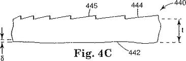
ウェットアウト防止面に用いることができる構造を有する別のタイプのフィルムが、図4Cに示されている。フィルム440は、上面445にフレネル構造444を有するフレネルレンズである。下面442は、ウェットアウト防止面である。
【0034】
図4A〜図4Cに示されているような別の構造を有するフィルムにおいて、ウェットアウト防止面を用いてもよいことを十分に理解されたい。たとえば、レンズまたは他の光屈折構造または光拡散構造などの他の構造が、フィルムの構造面に存在してもよい。
【0035】
さらに、本質的に偏光子、バルク拡散体、散乱フィルム、リターディションフィルムなどの面構造がないフィルムに、ウェットアウト防止面を用いてもよい。このようなフィルムの光学的な影響は一般に、構造面の屈折の影響に左右されるのではなく、フィルムのバルク内で生じる光学作用に基づく。下面464がウェットアウト防止面である場合の偏光フィルム460が、図4Dに示されている。屈折構造を持たないフィルムは各面462,464にウェットアウト防止面を備えていてもよいことを十分に理解されたい。
【0036】
フィルム460は、面462,464に略平行であるフィルム460の中心を通る仮想平面466を有するように示されている。各面462,464は、それぞれの範囲δ1,δ2の中にある平面466からの高さにおいて、全体に変動するように示されている。δ1,δ2は0μm〜5μmの範囲内にあるのが一般的であり、約1.5μmであればさらに一般的である。
【0037】
したがって、別の滑らかなフィルム面に対してウェットアウト防止特徴部を設けることは、ディスプレイにおける欠陥の低減のために利用されてもよいことを十分に理解されたい。これは、多くの異なるタイプのフィルムに適用可能である。このようなフィルムは、面に屈折構造を含んでもよく、フィルムを経た光の伝搬を左右するバルク光学作用の影響に基づいてもよい。ウェットアウト防止面を有するフィルムはまた、バルク効果および表面効果の組合せに基づいてもよい。
【0038】
ウェットアウト防止面を有するフィルムを用いた装置の1つの特定の実施形態が、図5Aの分解立体図に示されている。液晶ディスプレイ(LCD)照明モジュール500は、光を光導波路504の中に指向するため、光源として蛍光灯502および反射体503を用いる。光導波路は、下面507に拡散反射抽出ドット506を装備する。導波路504の上の任意の素子から再循環される任意の光を反射するために、広帯域の拡散反射体508が、光導波路504の下に配置される。蛍光灯502からの光は、光導波路504の側面に入射し、導波路504の面における内部反射によって光導波路504に沿って誘導される。多数の拡散光線512を形成するために、抽出ドット506の1つに入射する光線510が拡散反射される。
【0039】
抽出ドット506から上側に伝搬する光は、導波路504の上面513を通過する。導波路504から抽出された光をさらに拡散し、LCDディスプレイ524の次の照明をさらに均一にするために、拡散体514が光導波路の上に配置されてもよい。
【0040】
次に、下方向に延びている光は、図4Aの輝度強化フィルムに関して示されたプリズム構造と類似の上面にあるプリズム構造を有する下部輝度強化フィルム(BEF)516を通ってもよい。下部BEF516は、(たとえば図面の平面から)1次元に沿った光の発散を低減する。(たとえば、図面の平面内の)第2の次元に沿った光の発散を低減するために、下部BEF516の上に配置された上部BEF518は、下部BEF516のプリズム構造に対して約90°で指向されるプリズム構造を有する。上部BEF518または下部BEF516のいずれによって反射される光は、反射体508によって再循環される。交差されるBEFフィルム516,518の組は、光導波路504から抽出された光の全体の発散を低減する場合に効果的であると思われる。
【0041】
反射偏光フィルム520は、上部BEF518の上に配置される。反射偏光子は、1つの偏光の光を透過し、別の偏光の光を反射する。したがって、偏光フィルム520を通過する光は偏光される。偏光フィルム520によって反射される光は、反射体508によって再循環されてもよい。偏光フィルム520は、ウェットアウト防止の上面522を装備する。
【0042】
LCDマトリクス524が、偏光フィルム520の上に配置される。LCDマトリクスを通過する偏光が、たとえば、次に透過される画像の情報によって空間変調される。ウェットアウト防止面522は、偏光フィルム520とLCDマトリクス524との間のウェットアウトおよびニュートンリングの形成を低減するため、使用者によって見られる画像の品質が向上される。ウェットアウト防止面522の利用は、偏光フィルム520とLCDマトリクス524との間にウェットアウト低減カバーシートを含む必要性を回避する。
【0043】
上部BEF518と偏光フィルム520との間のカバーシートなどの別の素子が、モジュール500に備えられてもよい。
【0044】
図5Bは、本発明による光再指向フィルムを用いた別のタイプのディスプレイ550を示している。照明素子552からの光は、反射体554によって光導波路556の中に指向される。照明素子552は、他のタイプの素子を用いてもよいが、一般に蛍光管である。光導波路556は、楔形であるが、擬似楔形などの別の形状を用いることも可能である。光導波路556は、透明であってもよく、またはバルク拡散体を含んでもよい。
【0045】
小さな角度またはかすめ角で光導波路556から射出する光は、光再指向フィルム558に入射する。光再指向フィルム558は、線形プリズム562などの複数の線形プリズムを有する構造面の側面560を有する。線形プリズム562は、第1の側面564および第2の側面566を有する。光導波路556からの光は一般に、線形プリズム562の第1の側面564を経て再指向フィルム558に入射し、図5Cの光線565に関して示されるように、第2の側面564によって内部全反射される。内部全反射の後、光は、射出面568を通って再指向フィルム558から射出する。次に、光は、液晶ディスプレイなどの光ゲーティング装置570を通過してもよい。光学的欠陥が再指向フィルム568と光ゲーティング装置570との間に生じることを防止するために、再指向フィルム568の射出面568は、ウェットアウト防止面であってもよい。
【0046】
モジュール500,550の詳細は例示のために示されているに過ぎず、いかなる方式においてもウェットアウト防止面を有するフィルムの利用を制限することを目的としているわけではないことを十分に理解されたい。2つの光学面が互いに別の方法で接触し、ウェットアウトまたはニュートンリングを形成する場合に、さまざまな異なるタイプの光学系においてウェットアウト防止面を有するフィルムを用いることができる。
【0047】
光学フィルムは、型押、押出、流延および硬化、圧縮成形および射出成形をはじめとするさまざまな異なる方法によって一般に作製される。これらの方法は、フィルムにウェットアウト防止面を形成する場合に適している。たとえば、フィルム602が押出ローラ604によってダイ600を通って、貯槽601から引っ張り出される場合には、フィルムは、図6に示されているように、一定の寸法だけ離隔された1組のローラの間で流延されてもよい。フィルム602は、押出ローラ604と第2のローラ606の間で挟み込まれる。フィルム602が面構造を有する場合には、第2のローラ606は、フィルム602の上にパターンを型押しするための規定の面を備えたパターンローラであってもよい。たとえば、フィルム602は、図4Aに示されているように輝度強化フィルムとして作製される場合に、第2のローラ606はその面の周囲に、フィルム602の上面612に相補的なくぼみを形成する複数のプリズム構造608を具備する。パターンローラの直径の値は15cm〜60cmの範囲にあってもよい。押出ローラ604はまた、フィルムの下面618の上にパターンを型押しするために用いられる型押しパターンを具備してもよい。ローラ604,606の間を通過した後、フィルム602は、たとえば冷却気620の中で冷却され、ローラ604,606によってその上に型押しされたパターンを保持する。示された特定の実施形態において、フィルム618の下面にウェットアウト防止面を型押しするために、押出ローラ604は、高さが不規則に変化する面616を有する。
【0048】
上部ローラ606は、さまざまな異なるタイプの型押しパターンを具備することができる。上部ローラ606に用いられることができる型押しパターンの例には、輝度強化フィルム用のプリズムパターン、レンチキュラーフィルム用のレンチキュラーパターン、フレネルレンズ用のフレネルパターンが挙げられる。さらに、上部ローラ606にあるプリズム構造は、図6に示されているような回転方向に平行な方向ではなく、ローラ606の外周の回りに回転方向に垂直な方向に配置されることもできる。上部ローラ606はまた、平坦なフィルム面を形成するために滑らかであってもよく、またはフィルム602の上面612にウェットアウト防止パターンを型押しするための面を具備してもよい。これは必要条件ではないが、ウェットアウト防止面を形成するために、押出ローラ604の面は、不規則な型押しパターンを含んでもよい。両方のローラ604,606が不規則な型押しパターンを有する場合には、結果として生じるフィルムは2つのウェットアウト防止面を有する。
【0049】
1つ以上のウェットアウト防止面を有するフィルムの作製するために、シートを型押しする射出成形および圧縮成形をはじめとする別の解決策を取ってもよい。ある特定の解決策では、ウェブにかけられる型押し可能な材料のフィルムは、フィルムの上にパターン面の片割れを型押しするために、パターン面に対して圧縮するように保たれる。型押し可能な材料は、熱可塑性材料であってもよく、このようなフィルムは、その上に型押しされるパターンを有する材料を固体化させるために、パターン面に対して保持している間に冷却されることができるフィルムであってもよい。この解決策の変形において、型押し可能な材料は、パターン面に対する適切な場所、またはパターン面を除去した後に硬化される、または部分的に硬化される硬化性ポリマーであってもよい。
【0050】
ウェットアウト防止面を形成するための別の解決策において、フィルムは、その上にある不規則なパターンを有する母型を用いて射出成形されてもよい。結果として生じる射出成形フィルムは、母型の不規則なパターンと対になった片割れであるウェットアウト防止面を有する。別の解決策において、フィルムは、圧縮成形されてもよい。成形ツールは、成形される部分の上にウェットアウト防止面を形成する不規則な面を具備していてもよい。
【0051】
フィルムが型押しされた後、たとえば、反射防止コーティングなどを形成するためのコーティングなど、追加的な後処理の処置が施されてもよい。
【0052】
フィルムはまた、作製後、1つ以上のさまざまな異なる方法を用いて、延伸されてもよい。たとえば、1つの可能な方法は、ウェブが2組のローラの間に挟み込まれ、下流の組のローラが上流の組のローラより高速で回転する場合には、長さ延伸である。別の方法は、幅出しであり、たとえば、ウェブの両側にコンベヤーベルトのような方式で配置された連続クランプを用いて、フィルムのエッジを把持することを含む。クランプが前進するとき、連続クランプは離れるように移動し、規定の距離全体にフィルムを延伸する。下ウェブの方向に延伸しないのに対して、幅出しは一般に、一方向にのみ、たとえばウェブを横切るようにフィルムを延伸するために行われる。ウェブは一般に、フィルムにおいて所望の厚さまたは所望の分子配向を実現するのに十分な程度まで延伸される。フィルムの幅は、幅出し工程の2〜10倍の範囲にある係数によって増大されることができ、3〜8倍の範囲にある係数であればさらに一般的である。シートのエッジがフレームの側面に接着され、フレームの側面が引張られる場合には、フィルムはまた、延伸フレームにおいてウェブではなく、シートとして延伸されてもよい。
【0053】
延伸のときにはフィルム材料の体積が依然として本質的に一定のままであるため、フィルムの断面形状は、相当明確に定義された態様において変化する。フィルムはX倍だけ横延伸される場合には、断面積が同一であるため、フィルムの高さはX倍減少する。したがって、延伸されていないフィルムが一方の面に型押しされたウェットアウト防止パターンを有し、局所極大点と局所極小点との間の高さの平均差がYである場合には、延伸されたフィルムの局所極大点と局所極小点との間の高さの平均差は約Y/Xである。たとえば、延伸されていないフィルムが、局所極大点と局所極小点との間の高さの平均差が8μmであるウェットアウト防止面を有し、フィルムが4倍に延伸される場合には、フィルムが延伸された後、局所極大点と局所極小点との間の高さの平均差は、約2μmである。
【0054】
したがって、ウェットアウト防止面は、フィルムが延伸されるかどうかに応じて選択されるたとえば、平均ピーク高さ、平均ピーク間距離などの寸法を有するフィルムに形成される。延伸が行われない場合には、フィルムに形成される面は、所望のピーク高さおよび平均離隔距離を有する。しかし、たとえば、1次元において、フィルムが延伸されることになっている場合には、面に形成されるピーク高さは、所望の最終的なピーク高さのX倍である。尚、Xは延伸係数である。さらに、フィルム面に形成される延伸方向における平均ピーク間距離は、延伸方向における所望の最終的なピーク間郷里の1/X倍である。延伸が1次元にのみ行われる場合には、延伸方向に垂直な方向における平均ピーク間距離は変化しない。したがって、垂直方向における平均ピーク間距離は、延伸後、所望の値と同一の値を有するようにフィルムに形成される。これに関しては、以下に示される実施形態の詳細でさらに説明する。
【0055】
フィルムが2次元、たとえばウェブを横切る方向およびウェブに沿った方向に延伸される場合には、フィルムに形成される面の寸法は、延伸後のウェットアウト防止面の寸法が所望の制限内にあるように選択される。
【0056】
プリズム状フィルム、レンチキュラーフィルム、フレネルレンズを有するフィルムなどの構造を備えたフィルムを作製するために用いられるツールの原型は、ダイヤモンドターニング技術によって製作されることができる。これらの原型は、押出工程または流延および硬化工程によってフィルムを作製するために用いることができる。一般に、直線パターン用のツールは、ダイヤモンドターニングによってロールなどで知られる円筒ブランクに製作される。他の材料も用いることができるが、ロールの面は一般に、硬質銅から構成される。構造は、ロールの外周に連続パターンで形成される。特定の一実施形態において、ダイヤモンドツールがターニングロールを横断する方向に移動している間に、構造は、単独の連続切削がロールに施されるねじ切りとして公知である技術によって機械加工されることができる。形成されるべき構造が一定のピッチを備えている場合には、ツールは、ロールに沿って一定の速度で移動する。一般的なダイヤモンドターニング機は、ツールがロールを貫通する深さ、ツールがロールに対して形成する水平方向ならびに垂直方向の角度、ツールの横断速度の独立制御を行ってもよい。さらに、ダイヤモンドターニング機は、ロールの回転速度を制御することができる。同様の技術は、ウェットアウト防止型押ロールを製作するために適応させることができる。
【0057】
ウェットアウト防止面を型押しするためのロールを製作する方法が、図7に示されている。ドラム700は、ドラムドライブ704によって軸702を中心にして回転される。コンピュータ706は、ドラムドライブ704を制御し、ドラム700の現在の角度位置Ψを監視することもできる。制御コンピュータ706はまた、ダイヤモンド切削ツール708の移動および動作を制御する。コンピュータ706は、軸702に平行なz方向および軸702に向かって放射方向に向けられるx方向における移動のために切削ツールホルダに制御信号を送信する。コンピュータ706はまた、ツール708とドラム700の面との間の角度Πのための制御信号を送信することもできる。切削ツールのサイズおよび形状は、ロール700が作製に用いられる特定のタイプのフィルムに応じて選択される。
【0058】
一般に、コンピュータ706は、回転ドラム700に沿って移動するために、z方向に裁断ツール708を移動させる。x方向における切削ツール708の制御は、ドラム700の面に切削される深さを制御する。ダイヤモンド切削ツール708は、マウント712に接着される高速サーボ装置710に保持されることができる。マウント712は一般に、コンピュータ706による制御下で、x方向およびz方向に並進可能である。高速サーボ装置710はまた、x方向に切削ツール708を並進する。しかし、切削ツール708は、通常の機械加工ツールマウントでは通常得ることができない周波数で作動する。高速サーボ装置の応答の上限周波数は、数kHz〜数十kHzの範囲にある可能性があるが、通常の機械加工ツールマウントは一般に5Hz以下である。高速サーボ装置710がx方向に生じるストロークの長さは一般に短く、50μm未満であり、20μm未満である場合もある。ストロークの長さと上限周波数応答との間に相殺関係があってもよいことを十分に理解されたい。一般に、高速サーボ装置710は、x方向において切削ツール708の短距離の高速の往復運動を行うために用いられるのに対し、マウント712は、x方向において切削ツール708の長めの距離であるが、低速の往復運動を行うために用いられる。ウェットアウト防止面パターンは、ドラムに浅い溝をねじ切りすることによってドラムに切削される。すなわち、ドラム700の面に切削が施されている間に、切削ツール708はz方向に並進する。マウント712は、高速サーボ装置710より低い周波数帯に作動する第2のサーボ装置であってもよい。
【0059】
ドラム700において面の切削を制御するために、複数の異なる解決策を用いてもよい。図7に示される1つの解決策において、コンピュータ706は、zおよびオプションでΠに関する制御信号を発生する。コンピュータ706はまた、2つの成分を有する切削ツール708のための制御信号xも発生する。第1の成分x0は、高速サーボ装置710をx方向に並進するために、マウント712に向けられる徐々に変化する関数である。徐々に変化する関数は、たとえば正弦波または不規則であってもよい。第2の成分x1は、コンピュータによって生成される雑音関数であり、高速サーボ装置708をx方向において小さな高速かつ独立な不規則な時間の移動を行わせる。
【0060】
ロール700の面に結果と生じる不規則な切削点は、カッター708に対するロールの面の速度に左右されるロール外周の局所極小点の間の平均間隔と、x方向において切削ツール708の不規則な時間の往復運動の平均期間を有する。ドラム700の面は、フィルムの相補面を形成するため、ロール面の上の局所極小点は、フィルム面の局所極大点に対応する。ロール面の高さにおいて局所極小点の間の平均離隔距離が約150μmであり、ロール708の往復運動の間の平均時間が200μs(切削ツールの平均作動周波数5kHzに対応する)であるように選択される場合には、ロールの面の速度は、約0.75ms−1であるように選択される。
【0061】
さらに、高速サーボ装置710による高速のx方向の並進によって、切削ツール708のx位置の変更に関して、切削ツール708のx位置は、x0信号成分の制御下で、マウント712の低速のx方向の並進によって変更されてもよい。x0信号が、ロール700の回転速度の高調波または低調波のいずれでもない速度で変化する場合には、切削面の周期性における規則性は、避けられたように見える。マウント712の低速のx方向の並進は、高速サーボ装置710のストローク長より大きい距離だけロール700に切削される面の高さを変化させるために用いられてもよい。
【0062】
図8A〜図8Cは、ロール700の面の上にランダムパターンまたは擬似ランダムパターンを切削するために、コンピュータ706が高速サーボ装置710に送信することができる異なるタイプの制御信号の例を、時間に対してプロットされた電圧の関数として示している。
【0063】
図8Aにおいて、制御信号800は、パルス間の距離が不規則に変化する一定の振幅および幅を有する一連のパルスを含む。図8Bにおいて、制御信号802は、一定の振幅およびパルス間距離を有するが、幅が不規則に変化する一連のパルスを含む。図8Cにおいて、制御信号804は、一定の幅およびパルス間距離を有するが振幅が不規則に変化する一連のパルスを含む。
【0064】
信号800,802,804において生じる不規則に現れるパルスのパターンは、高速サーボ装置710によって、ロール700の面の上に切削される不規則に分散された局所極小点のそれぞれの匹敵するパターンに変換される。高速サーボ装置710に供給される制御信号における一連のパルスは、不規則に変化するパルス振幅、パルス幅、パルス間距離の任意の組合せを含むことができる。コンピュータ706から高速サーボ装置710にランダムまたは擬似ランダムに変化する制御信号を供給することの利点は、1つのロールに切削される不規則に生成されたパターンは、コンピュータ706でプログラムされ、別のロールで反復することができることである。
【0065】
パルス制御信号の別の利点には、高速サーボ装置710に発生する熱を低減することができること、ロール切削速度がよりたやすく増大することができること、設計者が切削工程を理解しモデルを製作することがよりたやすいことが挙げられる。
【0066】
ロール700を切削するために、切削ツール708の適切な並進を行うために、高速サーボ装置710に別のタイプの信号を送信してもよい。尚、図8A〜図8Cの例は、本発明を制限することを目的としたものではない。
【0067】
本発明の利点は、たとえばプリズム状フィルムにおけるプリズムの方向に平行な方向に面を傾斜することなど、ウェットアウト防止面の特性を一定の方向に対する特定の値であるように選択することができることであることは、上記で述べた。ウェットアウト防止面の延伸に関する別の実施形態において、ドラムを切削している間、局所極小点間の「上ねじ山(across−thread)」の離隔距離には何ら制限を加えないのに対し、面における局所極小点間の「下ねじ山(down−thread)」の離隔距離の範囲が、たとえば150μm〜200μmであるように選択することができる。不規則な特性のこのような延伸の選択は、たとえば、線形モアレ縞パターンなどの一次効果を避けるために有用であると思われる。
【0068】
ドラムにウェットアウト防止面を切削するための別の解決策は、図9に示されている。図7の構成要素と同一である構成要素は、同一の識別数字がつけられている。ドラム700が軸702を中心にして回転するとき、ドラム700の角度Ψの制御および監視を行うために、切削動作を制御するコンピュータ900は、ドラムドライブ704に接続される。コンピュータ900は、y方向における切削ツール708の移動を制御するための制御信号およびx方向における切削ツール708の比較的低速の移動用の低速x信号をマウント712に送信する。コンピュータ900はまた、切削ツール708とロール700の面との間の角度θを制御するために、制御信号を供給することができる。
【0069】
雑音源904は、一般に帯域通過フィルタ906を通過する雑音信号Inを発生する。x方向における切削ツール708の不規則かつ高速移動を実現するために、必要な場合には、フィルタリングされた雑音信号は、増幅器907で増幅され、高速サーボ装置710に高速x信号として印加される。
【0070】
雑音周波数の所望の範囲内にある周波数を通過するように、フィルタ906の通過帯域を調整することができる。たとえば、通過帯域は幅数kHzのウィンドウを超えて広がっていてもよく、1kHzまたは2kHz〜数十kHzの範囲の中心に合わせられていてもよい。周波数帯の中心は、ドラムの切削面の上の局所極小点の所望の平均間隔に応じて選択され、選択された通過帯域の幅は、局所極小点間の離隔距離の所望の隔たりに左右される。周波数帯の中心の選択は、高速サーボ装置710の必要なストローク長に左右されてもよい。一般に、作動周波数が増大すると、高速サーボ装置のストローク長は減少する。
【0071】
雑音源904からの信号はフィルタリングされるため、高速サーボ装置710に印加される信号は正確にランダムではないが、擬似ランダムであることを理解されたい。しかし、雑音信号の周波数を制限することは、高速x信号において統計的に最大周波数の偏位の発生を避ける。このような偏位は、極小点間の間隔が比較的長い部分に隣接する極小点間の間隔の比較的短い部分を有するロールにおいて生じる可能性があり、使用者に認識され得るディスプレイにおける欠陥を生じる恐れがある。
【0072】
図8に示されるようなシステムの特定の一実施形態において、半径64μmのダイヤモンドを有する切削ツール708が切削ピッチ40μmで用いられる。ドラム700の一回転中に、切削ピッチは、z方向に切削ツール708によって移動される距離である。切削ツールの深さは、ドラムの1.69回転ごとに約6μmの低速のx方向の並進を用いて変化がつけられる。これは、特にわずか1回転未満およびそれに近いサイクルを用いるときに見られるような周期性の問題に陥ることなく、深さが変化する一定のパターンを形成するために選択された比である。低速のx方向の並進に加えて、フィルタ付きのランダム雑音発生器を用いて発生された3ミクロンのランダム信号を印加する。フィルタは、4kHz〜5.6kHzの通過帯域で、雑音を通過させた。ドラムの面の速度は、ドラム面におけるピーク間の公称間隔または平均間隔が約170ミクロンであるように選択された。
【0073】
切削ツールを保持するための高速サーボ装置の特定の一実施形態が、図10に示されている。高速サーボ装置1000は、壁1006および背面1008を有するケース1004から延在する切削ツール1002を含む。切削ツール1002は、両面に圧電素子1010のスタックによって支持される。圧電スタック1010が高速に変化する電気信号によって励起されるとき、切削ツール1002は、ケース1004から延在する距離がわずかだけ変化するように移動させられる。圧電スタック1010は、一定のプログラムされた周波数の信号または不規則な周波数の信号によって励起されることができる。しかし、高さが不規則に変化するロール800に面を形成するために、圧電スタック1010に印加される信号は一般に、ランダムまたは擬似ランダムである。本願明細書で用いられるように、ランダムなる語は、擬似ランダムを含むことを理解されたい。
【0074】
実施形態
ウェットアウト防止面を有する反射偏光子フィルムは、その面が以下の態様で形成されたロールを用いて作製された。ロールは、面の速度約0.8ms−1で回転された。高速サーボ装置は、4kHz〜5.6kHzの範囲にある周波数を有する雑音源からの信号によって作動された。高速サーボ装置のストローク長は、約7μmであった。ロールの約1.69回転に等しい周期で約3μmの低速のx方向の並進が、高速サーボ装置に施された。半径約50μmのダイヤモンドツールは、約22μm〜28μmのピッチでロールの面に溝を切削した。切削の平均凹みは、約2μmであった。したがって、深さにおけるピークから谷までの最大の差は、約12μm(7+3+2μm)であった。隣接する溝間のピークのzの大きさは、ロールの周囲では滑らかに変化するのではなく、ピークの両側にある谷の相対切削深さに応じて幾分急速にz方向に変動した。しかし、z方向における局所極小点間の平均離隔距離は、zのピッチ、すなわち22μm〜28μmに等しかった。局所極小点間の平均離隔距離は、溝に沿った外周方向において約175μmであった。
【0075】
ロールは、図6に示された工程と同様の押出工程において、フィルムの上に面を形成するために用いられた。フィルムは、たとえば、開示された国際特許出願番号第WO95/17303号、第WO96/19347号、第WO95/17699号、第WO95/17692号、第WO95/17691号に記載されているようなPENおよびCoPENからなる交互の層から形成される多層反射偏光子フィルムであった。尚、これらの特許は本願明細書に引用によって参照されたものとする。フィルムが作製された後、フィルムは、約6倍横延伸された。したがって、延伸されたフィルムにおけるピークから谷までの最大高さは、約2μm(12÷6)であり、延伸方向における平均ピーク間距離は、132μm〜168μmであった。溝に沿った方向における平均ピーク間距離は、延伸の影響を受けず、依然として約175μmであった。
【0076】
フィルム上のウェットアウト防止面の実施形態は、図11Aおよび図11Bに示されている。フィルムは、25μmのピッチを用いて半径50μmのダイヤモンドツールを用いて切削されたドラムに形成された。切削ツールは、7μmの高周波ランダム動作および3μmの低周波数のx方向の動作を備えていた。フィルムは、作製後に約5倍延伸された。フィルムの断面積1.81mm(z軸)×1.36mm(y軸)の場合のウェットアウト防止面の3次元図が、図11Aに示されている。延伸方向は、y軸に沿った方向であった。図面は、サンプリングされた面領域全体にわたって、約1.2μmの高さの変動を示している。図11Bは、z軸に平行な面に沿ったラインに関する面の外形を示している。ラインの外形の長さに沿った高さにおける変動は、約0.3μmであった。
【0077】
上述したように、本発明は、ディスプレイシステムに適用することができ、バックライト式ディスプレイおよび背面映写スクリーンなどの複数の光学処理フィルムを有するディスプレイおよびスクリーンにおける見かけ上の欠陥を低減するのに特に有用であると考えられている。したがって、本発明は、上述した特定の実施形態に制限されると考えるべきではなく、添付の請求項に関して十分に説明されるように、本発明のすべての態様を網羅すると理解すべきである。本発明が適用可能であると思われるさまざまな修正、等価な工程のほか、さまざまな構造については、本発明が本願明細書の説明において狙いとしている当業者にはたやすく理解されるであろう。請求項は、このような修正および装置を網羅することを目的としている。
【図面の簡単な説明】
本発明は、添付の図面に関連して、本発明のさまざまな実施形態の以下の詳細な説明を考慮されば、さらに十分に理解されると思われる。
【図1A】 隣接するフィルムの間で生じる「ウェットアウト」の問題を示している。
【図1B】 隣接するフィルムの間で生じる「ウェットアウト」の問題を示している。
【図2A】 隣接するフィルムの間で形成されるニュートンリングの問題を示している。
【図2B】 隣接するフィルムの間で形成されるニュートンリングの問題を示している。
【図3A】 本発明の実施形態によるフィルム構造物を示している。
【図3B】 本発明の実施形態によるフィルム構造物を示している。
【図4A】 本発明によるウェットアウト低減面を備えた面構造のフィルムを示している。
【図4B】 本発明によるウェットアウト低減面を備えた面構造のフィルムを示している。
【図4C】 本発明によるウェットアウト低減面を備えた面構造のフィルムを示している。
【図4D】 本発明によるウェットアウト低減面を有する平面フィルムを示している。
【図5A】 本発明によるウェットアウト低減面を組込んだ照射装置の実施形態を示している。
【図5B】 本発明によるウェットアウト低減面を組込んだ照明装置の実施形態を示している。
【図5C】 図5Bに示された照明装置の光再指向フィルムを通過する光を示している。
【図6】 本発明によるフィルムを作製するための1工程を概略的に示している。
【図7】 本発明によるフィルムを作製するためのドラムを製作する第1の方法を概略的に示している。
【図8A】 本発明による切削ツールを制御するランダム制御信号を示している。
【図8B】 本発明による切削ツールを制御するランダム制御信号を示している。
【図8C】 本発明による切削ツールを制御するランダム制御信号を示している。
【図9】 本発明によるフィルムを作製するためのドラムを製作する第2の方法を示している。
【図10】 図7および図9に示されたドラムを製作する方法に利用するためのツールを示している。
【図11A】 本発明によって形成される面を有するフィルムの実施形態を示している。
【図11B】 本発明によって形成される面を有するフィルムの実施形態を示している。
本発明は、さまざまな変形および代替形態に修正されることが可能であるが、本明細書は、図面の一例として示され、詳細に説明される。しかし、記載された特定の実施形態に本発明を制限することを目的としていないことは理解されるべきである。別の見方をすれば、添付の請求項によって定義されているように、本発明の精神および範囲を逸脱することなく、すべての変形物、等価物および代替物を網羅しようとするものである。[0001]
Background art
The present invention relates primarily to light transmissive films, and more particularly to films that reduce the occurrence of defects in displays.
[0002]
The use of films for displays is well known. For example, in a backlight display, the brightness enhancement film uses a prism structure for directing light along the visual axis, and thus enhances the brightness of light recognized by the user. As another embodiment, to produce a screen with high contrast and high overall brightness while maintaining uniformly high brightness in certain selected directions while maintaining lower brightness in other directions Many different films can be utilized for a backlit computer display screen. For such a screen, a plurality of types of films such as a diffusion film combining a prismatic film or a lenticular film can be used.
[0003]
One problem with using film in displays is the very high requirement for good appearance. This is because such a display is seen at a close distance for a long time, and even a very small defect may be detected with the naked eye, which causes distraction of the user's attention. Eliminating such defects can be very costly in inspection time and material.
[0004]
Defects are manifest in a number of different ways. There are physical defects such as spots, lint, scratches and contaminants, and there are also defects that are optical phenomena. Among the most common optical phenomena are “wet-out” and Newton rings, where “wet-out” occurs when two surfaces are in optical contact with each other. In the case of light propagating from one film to the next, it effectively removes the change in refractive index, which makes the structural surface ineffective due to optical defects because the refractive properties of the structural surface become ineffective. Especially in the case of film, the effect of “wet out” is to create a mottled appearance on the screen Newton rings are the result of a slowly changing air gap between the two films. Yes, may be formed by dust particles between two films Newton rings may be formed in transmission or reflection. Result of ring, the user recognizes the contour patterns in the screen that might disturbed.
[0005]
In order to overcome the defect problem in multi-film display assemblies, several solutions have been taken. One solution only allows low yields of acceptable display assemblies made by conventional fabrication processes. This is clearly unacceptable in a competitive market. The second solution is to adopt a very clean and careful production procedure and to impose a strong quality control standard. This can improve yield and manufacturing costs are increased, including cleaning tools and inspection costs.
[0006]
Another solution for reducing defects is to introduce diffusers into the display, either surface diffusers or bulk diffusers. Such a diffuser can mask many drawbacks and increase the manufacturing yield at a low additional cost. However, the diffuser scatters light and reduces the on-axis brightness of the light perceived by the user, thus degrading performance.
[0007]
There is a continuing need to reduce the occurrence of defects in the display in order to maintain performance while improving manufacturing yield at a small additional cost.
[0008]
Disclosure of the invention
Primarily, the invention relates to such a film surface that can be used to reduce the occurrence of optical defects in displays using the film. More specifically, such surfaces have randomly extracted characteristics that reduce defects such as wetout, Newton rings, and the effects of moire fringes. The present invention also relates to a method for producing a film, a tool used for producing a film, and a method for producing the tool.
[0010]
In another embodiment, the present invention provides a film having a wet-out prevention surface overlying a first surface that does not include a regularly refracting structure, and a second surface opposite the first surface. Including. In another embodiment, the film comprises a first surface, a wet out reduction means disposed on the first surface to reduce wet out between the first surface and another optical surface. ,including
[0011]
In another embodiment of the present invention, the optical device includes a light source and a film having a wet-out prevention surface overlying the first surface that does not include a regularly refracting structure. The second optical element includes a second surface facing the first surface, and passes through the optical film from the light source and the second optical element.
[0012]
In another embodiment of the present invention, the method for producing an optical film includes forming a wet-out prevention surface on the first surface of the optical film.
[0013]
In another embodiment of the present invention, a method of making a drum for embossing a surface on a film is provided for a characteristic cutting tool to form a characteristic change that exists irregularly within a predetermined range. Rotating the drum around the rotation axis, cutting the surface of the drum using the cutting tool, and irregularly changing the cutting characteristics of the cutting tool. The drum for embossing the surface on the film does not include a regular structure and includes a surface having multiple local minimum points, and the surface property measurements are random within a predetermined range. Contains a significant value.
[0014]
The above disclosure of the present invention is not intended to represent each illustrated embodiment or every implementation of the present invention. The drawings and the following detailed description further illustrate these embodiments.
[0015]
Details of the invention
The present invention is applicable to optical processing films and appears to be particularly suitable for optical films for use with liquid crystal displays used in computer displays or monitors and the like. The invention is also useful in other areas where multiple optical processing films are used, such as rear projection screens and overhead projection displays. One advantage of the present invention is that it increases manufacturing yield by reducing the intensity of defects in the display area.
[0016]
For purposes of illustration, the present invention is described below for a particular application of a multi-film liquid crystal computer display. It should be appreciated that the use of the present invention is not very limited and that there is a wide range of applications having multiple optical processing films where the present invention may be useful.
[0017]
Wet-out and Newton rings are optical phenomena that cause defects in multilayer displays. 1A and 1B illustrate the problem of wet-out in the
[0018]
Another source of defects is the formation of Newton rings that can be displayed either in transmission or reflection. Newton rings may be formed in a
[0019]
It has been observed that when adjacent surfaces of different films are smooth and flat, multiple defects occur, including wet out and Newton rings. A solution for reducing such defects is to vary at least one height of the film surface in an irregular manner. This is illustrated, for example, in FIG. 3A where the
[0020]
The
[0021]
The irregularity in height prevents the formation of a wet-out region as shown in FIG. The
[0022]
Irregular changes in film surface height produce a number of other undesirable and favorable results in addition to wetout and Newton reduction. First, the film produced according to the present invention does not have the appearance of a high-performance transparent optical film. Instead, it has a seemingly turbid appearance that can hide some of the small defects in any structure of the film. Thereby, the yield of the manufacturing process can be remarkably improved. Second, the film of the present invention can also act to eliminate or hide moiré fringe patterns that result from interference between structures on different films in the display. Another important result is that the optical effects of different films, such as brightness enhancement, diffusion or collimation, are inherently affected in multilayer displays when the height at one or more film planes in the film stack is irregular. It can be made not to affect.
[0023]
For the purposes of this description, it is understood that surfaces with irregular heights work more than reducing wet-out, such as reducing Newton's rings. This is called “out prevention surface”. The wet-out prevention surface is generally flat in a large area that can generally be recognized by the user. In areas that are generally so small that they cannot be perceived by the user, there are many local maxima on the face that have peaks or heights on the face. The average difference in height between the local maximum point of the height on the surface and the local minimum point of the height on the intervening surface is generally small and is about 1 micron or 2 microns. Thus, when the wet-out prevention surface is placed against another smooth surface, the majority of the area above the wet-out prevention surface is from the contact with the second surface at a distance of a few microns or less. Hold away. The peak is in contact with the second surface and the area of each point of contact is small enough to prevent significant wet out at any one peak. The peaks may be irregularly separated, for example with an average separation between 50 μm and 500 μm, preferably between 100 μm and 250 μm. The peaks may have different heights within a certain range with an average height difference between the local maximum and local minimum of less than about 5 μm, preferably less than about 2 μm. The average separation distance between the local minimum point of the height and the local maximum point may be about 1.5 μm.
[0024]
Thus, there may be irregularities or irregularities in the distance between peaks. There may also be other irregularities in peak height. However, it is not a true irregularity in peak-to-peak distance or peak height. The value of the peak height and / or the distance between peaks may take a value existing in a preselected range, either randomly or pseudo-randomly. By placing the upper and lower bounds on the peak-to-peak distance and / or peak height, certain defects resulting from extreme values may statistically occur, but the peak-to-peak distance or peak height may be reduced.
[0025]
Another property of the anti-wet-out surface that may be able to vary in an irregular manner within the limits is the tilt angle of the surface reaching the local maximum. When the tilt angle is large, the light passing through the surface portion having a large tilt angle is refracted at a larger angle with respect to the vertical plane of the film than the light passing through the surface portion having a small tilt angle. This can affect the quality of the dispersion of the film, as films having surfaces with large tilt angles disperse light at larger angles. Further, the slope of the peak on the wet-out prevention surface does not need to be symmetric about the peak. For example, since the slope is large, the dispersion may be large with respect to the first axis, and the slope is small. The dispersion may be small with respect to the second axis orthogonal to the first axis. The tilt of the surface in a given direction of the film surface may be irregular within predetermined limits.
[0026]
Films made according to the present invention can also be made of any substantially transparent material. In many cases this can degrade the performance of the optical film, but bulk diffusing materials can also be incorporated into the film according to the invention. In addition, multiple layers of films and materials may be included in a film to form certain optical effects such as reflected polarization. A monolithic extruded film made of acrylic resin and polycarbonate is a strong candidate for film material. Also, if the structural surface is cast and cured on a substrate having a smooth and irregular height according to the present invention, the film may have a two-part configuration. For example, an ultraviolet curable acrylic resin cast on a polyester substrate may be used. Polyethylene terephthalate ("PET") films have been shown to work well as substrates that can be cured in structure. PET is often preferred for its mechanical and optical properties because it is stretched in the axial direction. A polyester film that can be used as a substrate is duPont ICI America's Inc. , Hopewell, Virginia trade name MELINEX TM It is available on the market under the name 617. Polyethylene naphthalate (PEN), either alone or as a copolymer with PET (known as CoPEN), has been shown to work well as a polymeric material in making optical films.
[0027]
A wet-out prevention surface can be provided on a variety of different types of optical films. For example, as shown in FIG. 4A, a prism-like
[0028]
The
[0029]
The thickness t of the
[0030]
As described above, the size of the Newton ring pattern depends on the average separation distance between local maximum points. The greater the distance, the more likely the Newton ring pattern will be visible. Therefore, it is advantageous to reduce the distance between the average maximum points. On the other hand, when the average height of the local maximum points is constant, a decrease in the distance between the average maximum points results in increasing the tilt angle of the surface. A larger surface tilt angle increases the diffusion of light through the film surface. There are other applications where surface diffusion must be minimized while surface diffusion may be acceptable in some applications. Therefore, to reduce wetout and Newton ring problems, as well as to reduce surface diffusion, it is possible to use a δ of about 1.5 μm and an average separation between local maxima in the range of 150 μm to 250 μm. it can. These values are provided only as suggested operating points and are not intended to limit the present invention.
[0031]
Another advantage of the present invention is that the wet-out prevention surface can be preferentially directed to structures on the other side of the film. For example, the wet-
[0032]
Another embodiment of a film having a structure that can be used for a wet-out prevention surface is shown in FIG. 4B. The
[0033]
Another type of film having a structure that can be used for a wet-out prevention surface is shown in FIG. 4C. The
[0034]
It should be appreciated that a wet out-preventing surface may be used in films having other structures as shown in FIGS. 4A-4C. For example, other structures such as lenses or other light refracting structures or light diffusing structures may be present on the structural surface of the film.
[0035]
Further, a wet-out prevention surface may be used for a film that is essentially free of a surface structure such as a polarizer, a bulk diffuser, a scattering film, and a retardation film. The optical effects of such films are generally not based on the effects of structural surface refraction, but are based on optical effects occurring in the bulk of the film. A
[0036]
[0037]
Thus, it should be appreciated that providing a wet-out prevention feature for another smooth film surface may be utilized for reducing defects in the display. This is applicable to many different types of film. Such films may include refractive structures on the surface and may be based on the influence of bulk optical effects that affect the propagation of light through the film. Films having a wet-out prevention surface may also be based on a combination of bulk and surface effects.
[0038]
One particular embodiment of an apparatus using a film having a wet-out prevention surface is shown in the exploded view of FIG. 5A. The liquid crystal display (LCD)
[0039]
Light propagating upward from the extraction dot 506 passes through the
[0040]
The downwardly extending light may then pass through a bottom brightness enhancement film (BEF) 516 having a prism structure on the top surface similar to the prism structure shown for the brightness enhancement film of FIG. 4A.
[0041]
The reflective
[0042]
An
[0043]
Another element such as a cover sheet between the
[0044]
FIG. 5B shows another type of
[0045]
Light emitted from the
[0046]
It should be appreciated that the details of
[0047]
Optical films are generally made by a variety of different methods including stamping, extrusion, casting and curing, compression molding and injection molding. These methods are suitable for forming a wet-out prevention surface on a film. For example, if the
[0048]
The
[0049]
Other solutions may be taken to produce films having one or more wet-out prevention surfaces, including injection molding and compression molding to emboss the sheet. In one particular solution, a film of embossable material that is applied to the web is kept compressed against the pattern surface to emboss a crack in the pattern surface on the film. The embossable material may be a thermoplastic material, such a film being held against the pattern surface to solidify the material having the pattern embossed thereon. It may be a film that can be cooled rapidly. In a variation of this solution, the embossable material may be a curable polymer that is cured or partially cured at a suitable location relative to the pattern surface or after removal of the pattern surface.
[0050]
In another solution for forming an anti-wetout surface, the film may be injection molded using a matrix having an irregular pattern thereon. The resulting injection-molded film has a wet-out prevention surface that is a half crack paired with an irregular pattern of the matrix. In another solution, the film may be compression molded. The molding tool may have an irregular surface that forms a wet-out prevention surface on the part to be molded.
[0051]
After the film is embossed, additional post-treatment treatments may be applied, such as a coating to form an anti-reflective coating or the like.
[0052]
The film may also be stretched after production using one or more of a variety of different methods. For example, one possible method is length stretching if the web is sandwiched between two sets of rollers and the downstream set of rollers rotates faster than the upstream set of rollers. Another method is tentering, including gripping the edges of the film using, for example, continuous clamps arranged in a manner like a conveyor belt on both sides of the web. As the clamp advances, the continuous clamp moves away and stretches the film over a defined distance. In contrast to not stretching in the direction of the lower web, tentering is generally done to stretch the film in only one direction, for example across the web. The web is generally stretched to a degree sufficient to achieve the desired thickness or desired molecular orientation in the film. The width of the film can be increased by a factor that is in the range of 2 to 10 times that of the tentering process, more commonly a factor that is in the range of 3 to 8 times. If the edges of the sheet are glued to the sides of the frame and the sides of the frame are pulled, the film may also be stretched as a sheet rather than a web in the stretch frame.
[0053]
Since the volume of the film material remains essentially constant when stretched, the cross-sectional shape of the film changes in a fairly well defined manner. If the film is transversely stretched by X times, the cross-sectional area is the same, so the film height decreases by X times. Therefore, when an unstretched film has a wet-out prevention pattern embossed on one side and the average difference in height between the local maximum and the local minimum is Y, the film is stretched. The average difference in height between the local maximum and local minimum of the film is about Y / X. For example, when an unstretched film has a wet-out prevention surface with an average height difference of 8 μm between the local maximum point and the local minimum point, and the film is stretched 4 times, After the film is stretched, the average difference in height between the local maximum point and the local minimum point is about 2 μm.
[0054]
Therefore, the wet-out prevention surface is formed on a film having dimensions such as an average peak height and an average peak-to-peak distance that are selected depending on whether the film is stretched. If stretching is not performed, the surface formed in the film has the desired peak height and average separation. However, for example, in one dimension, if the film is to be stretched, the peak height formed on the surface is X times the desired final peak height. X is a stretching coefficient. Furthermore, the average peak-to-peak distance in the stretching direction formed on the film surface is 1 / X times the desired final peak-to-peak hometown in the stretching direction. When stretching is performed only one-dimensionally, the average peak-to-peak distance in the direction perpendicular to the stretching direction does not change. Therefore, the average peak-to-peak distance in the vertical direction is formed on the film so as to have the same value as the desired value after stretching. This will be further explained in the details of the embodiment shown below.
[0055]
If the film is stretched in two dimensions, e.g., across the web and along the web, the dimensions of the surface formed in the film are within the desired limits for the dimensions of the wet-out prevention surface after stretching. Selected as
[0056]
The prototype of a tool used to make a film having a structure such as a prismatic film, a lenticular film, a film having a Fresnel lens, etc. can be manufactured by a diamond turning technique. These prototypes can be used to make films by extrusion processes or casting and curing processes. In general, a tool for a linear pattern is manufactured in a cylindrical blank known as a roll by diamond turning. The surface of the roll is generally composed of hard copper, although other materials can be used. The structure is formed in a continuous pattern on the outer periphery of the roll. In one particular embodiment, the structure may be machined by a technique known as threading in which a single continuous cut is applied to the roll while the diamond tool is moving in a direction across the turning roll. it can. If the structure to be formed has a constant pitch, the tool moves at a constant speed along the roll. A typical diamond turning machine may provide independent control of the depth at which the tool penetrates the roll, the horizontal and vertical angles that the tool forms with respect to the roll, and the traversing speed of the tool. Further, the diamond turning machine can control the rotation speed of the roll. Similar techniques can be adapted to produce wet-out-preventing push rolls.
[0057]
A method for manufacturing a roll for embossing the wet-out prevention surface is shown in FIG. The
[0058]
In general, the
[0059]
A number of different solutions may be used to control surface cutting in the
[0060]
The resulting irregular cutting points on the surface of the
[0061]
Furthermore, with respect to changing the x position of the
[0062]
FIGS. 8A-8C illustrate examples of different types of control signals that the
[0063]
In FIG. 8A, the
[0064]
The pattern of irregularly appearing pulses that occur in
[0065]
Another advantage of the pulse control signal is that heat generated in the high
[0066]
Another type of signal may be sent to the high
[0067]
An advantage of the present invention is that the characteristics of the wet-out prevention surface can be selected to be a specific value for a certain direction, such as inclining the surface in a direction parallel to the prism direction in the prismatic film. There is something mentioned above. In another embodiment relating to stretching of the wet-out prevention surface, while cutting the drum, there is no restriction on the "cross-thread" separation between local minima, The range of “down-thread” separation between local minima on the surface can be selected to be, for example, 150 μm to 200 μm. Such a stretch selection of irregular properties would be useful to avoid first order effects such as, for example, a linear moire fringe pattern.
[0068]
Another solution for cutting the wet-out prevention surface on the drum is shown in FIG. Components that are the same as those in FIG. 7 are given the same identification numbers. A
[0069]
The
[0070]
The passband of
[0071]
It should be understood that since the signal from
[0072]
In one particular embodiment of a system as shown in FIG. 8, a
[0073]
One particular embodiment of a high speed servo device for holding a cutting tool is shown in FIG. High
[0074]
Embodiment
A reflective polarizer film having a wet-out prevention surface was produced using a roll whose surface was formed in the following manner. Roll speed of surface is about 0.8ms -1 It was rotated by. The high speed servo device was activated by a signal from a noise source having a frequency in the range of 4 kHz to 5.6 kHz. The stroke length of the high-speed servo device was about 7 μm. A low speed x-direction translation of about 3 μm with a period equal to about 1.69 rotations of the roll was applied to the high speed servo device. A diamond tool having a radius of about 50 μm cut grooves on the surface of the roll at a pitch of about 22 μm to 28 μm. The average dent of cutting was about 2 μm. Therefore, the maximum difference in depth from the peak to the valley was about 12 μm (7 + 3 + 2 μm). The z magnitude of the peak between adjacent grooves did not change smoothly around the roll, but rather fluctuated in the z direction somewhat rapidly depending on the relative cutting depth of the valleys on either side of the peak. However, the average separation between local minima in the z direction was equal to the pitch of z, ie 22 μm to 28 μm. The average separation distance between the local minimum points was about 175 μm in the outer circumferential direction along the groove.
[0075]
The roll was used to form a surface on the film in an extrusion process similar to that shown in FIG. The films may include, for example, PEN as described in the disclosed International Patent Application Nos. WO95 / 17303, WO96 / 19347, WO95 / 17699, WO95 / 17692, WO95 / 17691. It was a multilayer reflective polarizer film formed from alternating layers of CoPEN. It should be noted that these patents are incorporated herein by reference. After the film was made, the film was stretched about 6 times. Therefore, the maximum height from the peak to the valley in the stretched film was about 2 μm (12 ÷ 6), and the average peak-to-peak distance in the stretching direction was 132 μm to 168 μm. The average peak-to-peak distance in the direction along the groove was not affected by stretching and was still about 175 μm.
[0076]
An embodiment of a wet-out prevention surface on the film is shown in FIGS. 11A and 11B. The film was formed into a drum cut with a diamond tool with a radius of 50 μm using a pitch of 25 μm. The cutting tool had a high frequency random motion of 7 μm and a low frequency x direction motion of 3 μm. The film was stretched about 5 times after making. FIG. 11A shows a three-dimensional view of the wet-out prevention surface when the film has a cross-sectional area of 1.81 mm (z-axis) × 1.36 mm (y-axis). The stretching direction was a direction along the y-axis. The drawing shows a height variation of about 1.2 μm over the sampled surface area. FIG. 11B shows the outline of the surface for the line along the surface parallel to the z-axis. The variation in height along the length of the line outline was about 0.3 μm.
[0077]
As mentioned above, the present invention can be applied to display systems and is particularly useful for reducing apparent defects in displays and screens having multiple optical processing films such as backlit displays and rear projection screens. It is considered to be. Accordingly, the invention is not to be considered as limited to the particular embodiments described above, but is to be understood as covering all aspects of the invention as fully described with reference to the appended claims. Various modifications, equivalent processes, and various structures that may be applicable to the present invention will be readily apparent to those skilled in the art to which the present invention is directed in the description of the specification. . The claims are intended to cover such modifications and devices.
[Brief description of the drawings]
The present invention will be more fully understood in view of the following detailed description of various embodiments of the invention in conjunction with the accompanying drawings.
FIG. 1A illustrates the “wet out” problem that occurs between adjacent films.
FIG. 1B illustrates the “wet out” problem that occurs between adjacent films.
FIG. 2A illustrates the problem of Newton rings formed between adjacent films.
FIG. 2B illustrates the problem of Newton rings formed between adjacent films.
FIG. 3A illustrates a film structure according to an embodiment of the present invention.
FIG. 3B illustrates a film structure according to an embodiment of the present invention.
4A shows a film having a face structure with a wet-out reducing surface according to the present invention. FIG.
FIG. 4B illustrates a film having a face structure with a wet-out reducing surface according to the present invention.
FIG. 4C illustrates a film having a face structure with a wet-out reducing surface according to the present invention.
FIG. 4D illustrates a planar film having a wet out reducing surface according to the present invention.
FIG. 5A illustrates an embodiment of an irradiator incorporating a wet out reduction surface according to the present invention.
FIG. 5B illustrates an embodiment of a lighting device incorporating a wet out reduction surface according to the present invention.
5C shows light passing through the light redirecting film of the illumination device shown in FIG. 5B.
FIG. 6 schematically shows one step for producing a film according to the invention.
FIG. 7 schematically shows a first method for producing a drum for producing a film according to the invention.
FIG. 8A shows a random control signal for controlling a cutting tool according to the present invention.
FIG. 8B shows a random control signal for controlling a cutting tool according to the present invention.
FIG. 8C shows a random control signal for controlling a cutting tool according to the present invention.
FIG. 9 shows a second method of making a drum for making a film according to the invention.
10 shows a tool for use in the method of making the drum shown in FIGS. 7 and 9. FIG.
FIG. 11A illustrates an embodiment of a film having a surface formed in accordance with the present invention.
FIG. 11B illustrates an embodiment of a film having a surface formed according to the present invention.
While the invention is amenable to various modifications and alternative forms, this specification has been shown by way of example in the drawings and will be described in detail. It should be understood, however, that the intention is not to limit the invention to the particular embodiments described. Viewed differently, it is intended to cover all variations, equivalents, and alternatives as defined by the appended claims without departing from the spirit and scope of the invention.
Claims (2)
高さの局所極大点に直近の前記第2の面の、前記線形配置のプリズムに対して垂直方向及び/又は水平方向の傾斜角が所定の範囲内においてランダムな値を有し、
前記線型配置のプリズムに対して垂直方向の傾斜角は、前記線型配置のプリズムに対して水平方向の傾斜角よりも小さいことを特徴とする光学フィルム。A first surface having a series of linearly arranged prisms, and a second surface facing the first surface and not including a regular structure, wherein the second surface has a plurality of With local maxima of height,
The inclination angle in the vertical direction and / or the horizontal direction with respect to the linearly arranged prism of the second surface closest to the local maximum point of height has a random value within a predetermined range,
An optical film , wherein an inclination angle in a vertical direction with respect to the linearly arranged prism is smaller than an inclination angle in a horizontal direction with respect to the linearly arranged prism .
Applications Claiming Priority (3)
| Application Number | Priority Date | Filing Date | Title |
|---|---|---|---|
| US09/246,970 US6322236B1 (en) | 1999-02-09 | 1999-02-09 | Optical film with defect-reducing surface and method for making same |
| US09/246,970 | 1999-02-09 | ||
| PCT/US1999/011580 WO2000048037A2 (en) | 1999-02-09 | 1999-05-26 | Optical film with defect-reducing surface and method for making same |
Publications (3)
| Publication Number | Publication Date |
|---|---|
| JP2002536702A JP2002536702A (en) | 2002-10-29 |
| JP2002536702A5 JP2002536702A5 (en) | 2006-07-13 |
| JP4480279B2 true JP4480279B2 (en) | 2010-06-16 |
Family
ID=22932967
Family Applications (1)
| Application Number | Title | Priority Date | Filing Date |
|---|---|---|---|
| JP2000598892A Expired - Fee Related JP4480279B2 (en) | 1999-02-09 | 1999-05-26 | Optical film having a surface for reducing defects |
Country Status (9)
| Country | Link |
|---|---|
| US (2) | US6322236B1 (en) |
| EP (1) | EP1159645A1 (en) |
| JP (1) | JP4480279B2 (en) |
| KR (2) | KR100623536B1 (en) |
| CN (1) | CN1161250C (en) |
| AU (1) | AU4099299A (en) |
| BR (1) | BR9917056A (en) |
| CA (1) | CA2359118A1 (en) |
| WO (1) | WO2000048037A2 (en) |
Families Citing this family (194)
| Publication number | Priority date | Publication date | Assignee | Title |
|---|---|---|---|---|
| DE69435173D1 (en) | 1993-12-21 | 2009-01-15 | Minnesota Mining & Mfg | Multilayer optical film |
| US5882774A (en) | 1993-12-21 | 1999-03-16 | Minnesota Mining And Manufacturing Company | Optical film |
| US6498683B2 (en) * | 1999-11-22 | 2002-12-24 | 3M Innovative Properties Company | Multilayer optical bodies |
| US7023602B2 (en) | 1999-05-17 | 2006-04-04 | 3M Innovative Properties Company | Reflective LCD projection system using wide-angle Cartesian polarizing beam splitter and color separation and recombination prisms |
| US6486997B1 (en) | 1997-10-28 | 2002-11-26 | 3M Innovative Properties Company | Reflective LCD projection system using wide-angle Cartesian polarizing beam splitter |
| US6926952B1 (en) * | 1998-01-13 | 2005-08-09 | 3M Innovative Properties Company | Anti-reflective polymer constructions and method for producing same |
| CN1104325C (en) * | 1998-01-13 | 2003-04-02 | 美国3M公司 | Modified copolyesters and improved multilayer reflective films |
| US6515785B1 (en) * | 1999-04-22 | 2003-02-04 | 3M Innovative Properties Company | Optical devices using reflecting polarizing materials |
| US6845212B2 (en) * | 1999-10-08 | 2005-01-18 | 3M Innovative Properties Company | Optical element having programmed optical structures |
| US6356391B1 (en) * | 1999-10-08 | 2002-03-12 | 3M Innovative Properties Company | Optical film with variable angle prisms |
| US7046905B1 (en) | 1999-10-08 | 2006-05-16 | 3M Innovative Properties Company | Blacklight with structured surfaces |
| US6449093B2 (en) | 1999-10-12 | 2002-09-10 | 3M Innovative Properties Company | Optical bodies made with a birefringent polymer |
| TW526348B (en) * | 2000-01-13 | 2003-04-01 | Nitto Denko Corp | Optical film and liquid-crystal display device |
| JP2001194534A (en) * | 2000-01-13 | 2001-07-19 | Nitto Denko Corp | Light guide plate and method of manufacturing the same |
| EP1143269B1 (en) * | 2000-01-13 | 2007-03-14 | Nitto Denko Corporation | Optical path changing polarizer |
| JP4609962B2 (en) | 2000-02-02 | 2011-01-12 | 日東電工株式会社 | Optical film |
| JP4442836B2 (en) | 2000-02-02 | 2010-03-31 | 日東電工株式会社 | Optical film |
| JP2001228315A (en) * | 2000-02-14 | 2001-08-24 | Nitto Denko Corp | Reflector and liquid crystal display |
| US8054416B2 (en) | 2000-08-15 | 2011-11-08 | Reflexite Corporation | Light polarizer |
| WO2002014909A2 (en) * | 2000-08-15 | 2002-02-21 | Reflexite Corporation | A light polarizer |
| US7230764B2 (en) * | 2000-08-18 | 2007-06-12 | Reflexite Corporation | Differentially-cured materials and process for forming same |
| JP2004506547A (en) | 2000-08-18 | 2004-03-04 | リフレキサイト・コーポレーション | Differentially cured material and method of forming the material |
| US20040190102A1 (en) * | 2000-08-18 | 2004-09-30 | Mullen Patrick W. | Differentially-cured materials and process for forming same |
| JP2002131552A (en) | 2000-10-24 | 2002-05-09 | Nitto Denko Corp | Light guide plate, surface light source device and reflection type liquid crystal display device |
| US6673425B1 (en) * | 2000-10-27 | 2004-01-06 | 3M Innovative Properties Company | Method and materials for preventing warping in optical films |
| US6697130B2 (en) * | 2001-01-16 | 2004-02-24 | Visteon Global Technologies, Inc. | Flexible led backlighting circuit |
| JP4662402B2 (en) | 2001-03-12 | 2011-03-30 | 日東電工株式会社 | Light guide plate for front light for both external light and illumination modes, surface light source device for front light for both external light and illumination modes, and front light type reflective liquid crystal display device for both external light and illumination modes |
| JP2003014938A (en) * | 2001-04-12 | 2003-01-15 | Mitsubishi Engineering Plastics Corp | Light guide plate made of transparent resin and molding method thereof, nesting, mold assembly, and planar light source device |
| US6880946B2 (en) * | 2002-01-15 | 2005-04-19 | Reflexite Corporation | Grooved optical microstructure light collimating films |
| TWI237725B (en) | 2002-01-23 | 2005-08-11 | Sony Corp | Image display device and image projector device |
| JP3963750B2 (en) * | 2002-03-25 | 2007-08-22 | 日本電産サンキョー株式会社 | Curved cutting method |
| US20040043234A1 (en) * | 2002-05-10 | 2004-03-04 | Grant Hay | Light management films and articles thereof |
| US7364314B2 (en) * | 2002-05-15 | 2008-04-29 | Reflexite Corporation | Optical structures |
| US6862141B2 (en) | 2002-05-20 | 2005-03-01 | General Electric Company | Optical substrate and method of making |
| US7180672B2 (en) * | 2002-05-20 | 2007-02-20 | General Electric Company | Optical substrate and method of making |
| US7859759B2 (en) * | 2002-05-20 | 2010-12-28 | Sabic Innovative Plastics Ip B.V. | Film, backlight displays, and methods for making the same |
| JP3937945B2 (en) * | 2002-07-04 | 2007-06-27 | セイコーエプソン株式会社 | Display device and electronic apparatus equipped with the same |
| US20040130057A1 (en) * | 2002-08-02 | 2004-07-08 | Reza Mehrabi | Process and apparatus for microreplication |
| US8070303B2 (en) * | 2002-08-08 | 2011-12-06 | Reflexite Corporation | Optical structures including polyurea |
| US6908202B2 (en) * | 2002-10-03 | 2005-06-21 | General Electric Company | Bulk diffuser for flat panel display |
| US6811274B2 (en) * | 2002-12-04 | 2004-11-02 | General Electric Company | Polarization sensitive optical substrate |
| US7125131B2 (en) * | 2002-12-06 | 2006-10-24 | General Electric Company | Brightness enhancement film with improved view angle |
| US6952627B2 (en) * | 2002-12-18 | 2005-10-04 | General Electric Company | Method and apparatus for fabricating light management substrates |
| TWI289708B (en) | 2002-12-25 | 2007-11-11 | Qualcomm Mems Technologies Inc | Optical interference type color display |
| EP1583657A1 (en) * | 2003-01-06 | 2005-10-12 | Avery Dennison Corporation | Embossed oriented optical films |
| US7236217B2 (en) * | 2003-01-16 | 2007-06-26 | 3M Innovative Properties Company | Package of optical films with zero-gap bond outside viewing area |
| JP2006525553A (en) | 2003-05-02 | 2006-11-09 | リフレキサイト コーポレイション | Optical reorientation optical structure |
| US6846089B2 (en) * | 2003-05-16 | 2005-01-25 | 3M Innovative Properties Company | Method for stacking surface structured optical films |
| US7413336B2 (en) * | 2003-08-29 | 2008-08-19 | 3M Innovative Properties Company | Adhesive stacking for multiple optical films |
| US20050130759A1 (en) * | 2003-12-12 | 2005-06-16 | Hayden Mark X. | Sports shaft with variable contour |
| US7072092B2 (en) * | 2003-12-31 | 2006-07-04 | General Electric Company | Optical substrate with modulated structure |
| US7147358B2 (en) | 2003-12-31 | 2006-12-12 | 3M Innovative Properties Company | Cover removal tab for optical products |
| US7342705B2 (en) | 2004-02-03 | 2008-03-11 | Idc, Llc | Spatial light modulator with integrated optical compensation structure |
| US20050238852A1 (en) * | 2004-04-23 | 2005-10-27 | Naoki Nakayama | Optical products for displays |
| TWI304486B (en) * | 2006-10-19 | 2008-12-21 | Efun Technology Co Ltd | Brightness enhancement film having curved prism units and matte |
| DE102004038571A1 (en) * | 2004-08-06 | 2006-02-23 | Breyer Gmbh Maschinenfabrik | Method for producing sheets of thermoplastically extruded plastics |
| US7212345B2 (en) * | 2004-09-13 | 2007-05-01 | Eastman Kodak Company | Randomized patterns of individual optical elements |
| US7630123B2 (en) | 2004-09-27 | 2009-12-08 | Qualcomm Mems Technologies, Inc. | Method and device for compensating for color shift as a function of angle of view |
| US7278771B2 (en) | 2004-11-22 | 2007-10-09 | 3M Innovative Properties Company | Optical film |
| US7163308B2 (en) * | 2004-11-22 | 2007-01-16 | Ferrari John S | Hand worn illuminated framework |
| GB0427607D0 (en) * | 2004-12-16 | 2005-01-19 | Microsharp Corp Ltd | Structured optical film |
| US7339635B2 (en) * | 2005-01-14 | 2008-03-04 | 3M Innovative Properties Company | Pre-stacked optical films with adhesive layer |
| US20060226583A1 (en) * | 2005-04-04 | 2006-10-12 | Marushin Patrick H | Light directing film |
| US20060257678A1 (en) * | 2005-05-10 | 2006-11-16 | Benson Olester Jr | Fiber reinforced optical films |
| TW200734699A (en) | 2005-11-05 | 2007-09-16 | 3M Innovative Properties Co | Optical films comprising high refractive index and antireflective coatings |
| US20070103910A1 (en) * | 2005-11-08 | 2007-05-10 | Eastman Kodak Company | Light redirecting films having multiple layers and an adhesion layer |
| US20070110386A1 (en) * | 2005-11-12 | 2007-05-17 | Tien-Hon Chiang | Device having combined diffusing, collimating, and color mixing light control function |
| US7350441B2 (en) * | 2005-11-15 | 2008-04-01 | 3M Innovative Properties Company | Cutting tool having variable movement at two simultaneously independent speeds in an x-direction into a work piece for making microstructures |
| US7290471B2 (en) * | 2005-11-15 | 2007-11-06 | 3M Innovative Properties Company | Cutting tool having variable rotation about a y-direction transversely across a work piece for making microstructures |
| US7575152B2 (en) * | 2005-11-15 | 2009-08-18 | E2Interactive, Inc. | Temporary value card method and system |
| US7350442B2 (en) * | 2005-11-15 | 2008-04-01 | 3M Innovative Properties Company | Cutting tool having variable movement in a z-direction laterally along a work piece for making microstructures |
| US7293487B2 (en) * | 2005-11-15 | 2007-11-13 | 3M Innovative Properties Company | Cutting tool having variable and independent movement in an x-direction and a z-direction into and laterally along a work piece for making microstructures |
| US7777832B2 (en) * | 2005-11-18 | 2010-08-17 | 3M Innovative Properties Company | Multi-function enhancement film |
| EP1793263A1 (en) | 2005-12-01 | 2007-06-06 | Emphasis Materials, Inc. | Light intensity and/or colour distribution correcting element for an illumination system whose function is correlated to the incident light distribution |
| US7328638B2 (en) * | 2005-12-27 | 2008-02-12 | 3M Innovative Properties Company | Cutting tool using interrupted cut fast tool servo |
| US20070153384A1 (en) * | 2005-12-30 | 2007-07-05 | Ouderkirk Andrew J | Reinforced reflective polarizer films |
| US20070153162A1 (en) * | 2005-12-30 | 2007-07-05 | Wright Robin E | Reinforced reflective polarizer films |
| US7366393B2 (en) | 2006-01-13 | 2008-04-29 | Optical Research Associates | Light enhancing structures with three or more arrays of elongate features |
| US7866871B2 (en) | 2006-01-13 | 2011-01-11 | Avery Dennison Corporation | Light enhancing structures with a plurality of arrays of elongate features |
| US7674028B2 (en) | 2006-01-13 | 2010-03-09 | Avery Dennison Corporation | Light enhancing structures with multiple arrays of elongate features of varying characteristics |
| US20070237938A1 (en) * | 2006-03-31 | 2007-10-11 | 3M Innovative Properties Company | Reinforced Optical Films |
| US20080274293A1 (en) * | 2006-03-31 | 2008-11-06 | 3M Innovative Properties Company | Spiral Multilayer Fibers |
| US7327923B2 (en) * | 2006-03-31 | 2008-02-05 | 3M Innovative Properties Company | Spiral multilayer fibers |
| US20070236938A1 (en) * | 2006-03-31 | 2007-10-11 | 3M Innovative Properties Company | Structured Composite Optical Films |
| JP4079979B2 (en) | 2006-04-19 | 2008-04-23 | ファナック株式会社 | Processing equipment |
| US7677146B2 (en) * | 2006-05-10 | 2010-03-16 | 3M Innovative Properties Company | Cutting tool using one or more machined tool tips in a continuous or interrupted cut fast tool servo |
| US20070281129A1 (en) * | 2006-06-06 | 2007-12-06 | Chi Kwong Chan | Diffuser films and methods for making and using the same |
| US20080049330A1 (en) * | 2006-08-25 | 2008-02-28 | 3M Innovative Properties Company | Light directing laminate |
| US7773834B2 (en) | 2006-08-30 | 2010-08-10 | 3M Innovative Properties Company | Multilayer polarizing fibers and polarizers using same |
| US7599592B2 (en) | 2006-08-30 | 2009-10-06 | 3M Innovative Properties Company | Polymer fiber polarizers with aligned fibers |
| US8872085B2 (en) | 2006-10-06 | 2014-10-28 | Qualcomm Mems Technologies, Inc. | Display device having front illuminator with turning features |
| CN101600901A (en) | 2006-10-06 | 2009-12-09 | 高通Mems科技公司 | Optical loss structure integrated in illumination device of display |
| EP1958010A2 (en) | 2006-10-10 | 2008-08-20 | Qualcomm Mems Technologies, Inc | Display device with diffractive optics |
| US7628100B2 (en) | 2007-01-05 | 2009-12-08 | 3M Innovative Properties Company | Cutting tool using one or more machined tool tips with diffractive features in a continuous or interrupted cut fast tool servo |
| US20080200088A1 (en) * | 2007-02-21 | 2008-08-21 | Chong Pyung An | Method for reducing interference fringes in a display device |
| US20080252202A1 (en) * | 2007-04-11 | 2008-10-16 | General Electric Company | Light-emitting device and article |
| KR100905241B1 (en) | 2007-04-13 | 2009-07-01 | 엘지전자 주식회사 | Optical film including a plurality of structures and a backlight unit comprising the same |
| US7604381B2 (en) * | 2007-04-16 | 2009-10-20 | 3M Innovative Properties Company | Optical article and method of making |
| EP2162705A4 (en) * | 2007-06-19 | 2014-02-19 | 3M Innovative Properties Co | Systems and methods for fabricating displacement scales |
| US8525954B2 (en) * | 2007-06-27 | 2013-09-03 | General Electric Company | Three-dimensional display article |
| US20090034268A1 (en) * | 2007-08-01 | 2009-02-05 | 3M Innovative Properties Company | Light management assembly |
| US9180524B2 (en) | 2007-08-06 | 2015-11-10 | 3M Innovative Properties Company | Fly-cutting head, system and method, and tooling and sheeting produced therewith |
| US20090041553A1 (en) * | 2007-08-06 | 2009-02-12 | 3M Innovative Properties Company | Fly-cutting system and method, and related tooling and articles |
| WO2009028226A1 (en) * | 2007-08-28 | 2009-03-05 | Sharp Kabushiki Kaisha | Method for manufacturing optical member, parent material for manufacture of optical member, transfer mold, lighting system for display device, display device, and television receiver |
| CN101835597B (en) * | 2007-09-21 | 2013-05-22 | 3M创新有限公司 | Optical film |
| US7742673B2 (en) * | 2007-09-28 | 2010-06-22 | General Electric Company | Thermal mangement article having thermal wave guide |
| US7898176B2 (en) * | 2007-09-28 | 2011-03-01 | General Electric Company | Fluidic thermal management article and method |
| US8058802B2 (en) * | 2007-09-28 | 2011-11-15 | General Electric Company | Thermal management article and method |
| US7669508B2 (en) * | 2007-10-29 | 2010-03-02 | 3M Innovative Properties Company | Cutting tool using one or more machined tool tips with diffractive features |
| US8068710B2 (en) | 2007-12-07 | 2011-11-29 | Qualcomm Mems Technologies, Inc. | Decoupled holographic film and diffuser |
| US20090147361A1 (en) * | 2007-12-07 | 2009-06-11 | 3M Innovative Properties Company | Microreplicated films having diffractive features on macro-scale features |
| JP5579082B2 (en) * | 2008-03-03 | 2014-08-27 | エルジー・ケム・リミテッド | Optical film and manufacturing method |
| WO2009124107A1 (en) | 2008-04-02 | 2009-10-08 | 3M Innovative Properties Company | Light directing film and method for making the same |
| EP2120070B1 (en) | 2008-05-16 | 2014-03-12 | LG Electronics Inc. | Optical sheet, backlight unit, and liquid crystal display |
| US8068187B2 (en) | 2008-06-18 | 2011-11-29 | 3M Innovative Properties Company | Stereoscopic 3D liquid crystal display apparatus having a double sided prism film comprising cylindrical lenses and non-contiguous prisms |
| US8847185B2 (en) | 2008-12-29 | 2014-09-30 | 3M Innovative Properties Company | Phase-locked web position signal using web fiducials |
| JP4930540B2 (en) * | 2009-04-13 | 2012-05-16 | ソニー株式会社 | Surface light emitting device and liquid crystal display device |
| US20100302218A1 (en) | 2009-05-29 | 2010-12-02 | Qualcomm Mems Technologies, Inc. | Illumination devices and methods of fabrication thereof |
| JP5823958B2 (en) | 2009-06-02 | 2015-11-25 | スリーエム イノベイティブ プロパティズ カンパニー | Light re-deflecting film and display using the film |
| KR101116140B1 (en) * | 2009-07-16 | 2012-03-06 | 엘지이노텍 주식회사 | Regular pattern optical sheet |
| US8882323B2 (en) | 2009-08-12 | 2014-11-11 | 3M Innovative Properties Company | Lightguide |
| KR20120061911A (en) | 2009-08-25 | 2012-06-13 | 쓰리엠 이노베이티브 프로퍼티즈 컴파니 | Light redirecting film and display system incorporating same |
| JPWO2011068212A1 (en) * | 2009-12-03 | 2013-04-18 | 大日本印刷株式会社 | Optical sheet roll, and optical sheet roll, optical sheet, and display device manufacturing method |
| WO2011084303A2 (en) | 2009-12-17 | 2011-07-14 | 3M Innovative Properties Company | Light redirecting constructions |
| CN102656489B (en) | 2009-12-17 | 2015-09-02 | 3M创新有限公司 | Light-redirecting film lamilated body |
| KR101214648B1 (en) * | 2010-04-13 | 2012-12-24 | 주식회사 엘지화학 | Condensing film having excellent prevention property of blocking and moire, backlight unit and display device comprising the same |
| SG185417A1 (en) | 2010-05-07 | 2012-12-28 | 3M Innovative Properties Co | Antireflective films comprising microstructured surface |
| WO2012018705A2 (en) | 2010-08-05 | 2012-02-09 | 3M Innovative Properties Company | Multilayer film comprising matte surface layer and articles |
| US8902484B2 (en) | 2010-12-15 | 2014-12-02 | Qualcomm Mems Technologies, Inc. | Holographic brightness enhancement film |
| US20120200816A1 (en) * | 2011-02-04 | 2012-08-09 | Guardian Industries Corp. | Electronic devices having reduced susceptibility to newton rings, and/or methods of making the same |
| EP2734872A4 (en) | 2011-07-19 | 2015-04-15 | 3M Innovative Properties Co | Dual-sided daylight redirecting film |
| US9618791B2 (en) | 2011-11-23 | 2017-04-11 | 3M Innovative Properties Company | Optical stack with asymmetric diffuser |
| WO2013096324A1 (en) | 2011-12-21 | 2013-06-27 | 3M Innovative Properties Company | Optical film stack |
| US9389355B2 (en) | 2012-03-20 | 2016-07-12 | 3M Innovative Properties Company | Structured optical film |
| US9850405B2 (en) | 2013-10-02 | 2017-12-26 | 3M Innovative Properties Company | Article comprising polyacrylate pressure sensitive primer and adhesive comprising polyacrylate component |
| WO2015050751A1 (en) | 2013-10-02 | 2015-04-09 | 3M Innovative Properties Company | Articles and methods comprising polyacrylate primer with nitrogen-containing polymer |
| CN105612438B (en) | 2013-10-02 | 2018-12-14 | 3M创新有限公司 | Microstructured diffuser including first microstructured layer and coating, optical stack and method |
| US9563006B2 (en) * | 2014-02-07 | 2017-02-07 | Rambus Delaware Llc | Lighting assembly having anti-wetting component interposed between light guide and reflector |
| US9778407B2 (en) | 2014-04-16 | 2017-10-03 | 3M Innovative Properties Company | Light guide |
| US9599766B2 (en) | 2014-04-16 | 2017-03-21 | 3M Innovative Properties Company | Laminated display unit |
| CN107003436B (en) | 2014-06-13 | 2020-02-14 | 3M创新产权公司 | Optical stack structure for flicker reduction |
| KR102387234B1 (en) | 2014-06-13 | 2022-04-18 | 쓰리엠 이노베이티브 프로퍼티즈 컴파니 | Optical stacks for sparkle reduction |
| US9919339B2 (en) | 2014-06-18 | 2018-03-20 | 3M Innovation Properties Company | Optical film |
| US9507162B1 (en) | 2014-09-19 | 2016-11-29 | Amazon Technologies, Inc. | Display component assembly |
| CN107003439B (en) | 2014-10-20 | 2019-04-23 | 3M创新有限公司 | Room facing light redirecting film with glare reduction |
| JP7009992B2 (en) | 2014-10-20 | 2022-01-26 | スリーエム イノベイティブ プロパティズ カンパニー | Micro-optical layer and method including adiabatic glazing unit and micro-structured diffuser |
| EP3210057B1 (en) | 2014-10-20 | 2020-08-26 | 3M Innovative Properties Company | Sun-facing light redirecting films with reduced glare |
| US9829617B2 (en) | 2014-11-10 | 2017-11-28 | Light Polymers Holding | Polymer-small molecule film or coating having reverse or flat dispersion of retardation |
| US10001587B2 (en) | 2015-03-27 | 2018-06-19 | 3M Innovative Properties Company | Brightness enhancement film |
| CN107810433B (en) | 2015-06-30 | 2021-03-05 | 3M创新有限公司 | Insulating glazing unit and microoptical layer including microstructured anisotropic diffuser and method |
| US9856172B2 (en) | 2015-08-25 | 2018-01-02 | Light Polymers Holding | Concrete formulation and methods of making |
| JP7000674B2 (en) * | 2015-12-01 | 2022-01-19 | 東洋製罐グループホールディングス株式会社 | Mold |
| JP2019501416A (en) * | 2015-12-09 | 2019-01-17 | スリーエム イノベイティブ プロパティズ カンパニー | Optical laminate |
| KR20180004707A (en) | 2016-06-09 | 2018-01-12 | 쓰리엠 이노베이티브 프로퍼티즈 컴파니 | Optical system |
| US10663745B2 (en) | 2016-06-09 | 2020-05-26 | 3M Innovative Properties Company | Optical system |
| KR102395414B1 (en) | 2016-06-09 | 2022-05-09 | 쓰리엠 이노베이티브 프로퍼티즈 컴파니 | Display systems and light guides |
| WO2018017552A1 (en) | 2016-07-22 | 2018-01-25 | 3M Innovative Properties Company | Structured film and articles thereof |
| JP7115810B2 (en) | 2017-02-20 | 2022-08-09 | スリーエム イノベイティブ プロパティズ カンパニー | Self-wetting adhesive composition |
| WO2018152467A1 (en) | 2017-02-20 | 2018-08-23 | 3M Innovative Properties Company | Self-wetting adhesive composition |
| US11662509B2 (en) | 2017-03-02 | 2023-05-30 | 3M Innovative Properties Company | Dynamic reflected color film with low optical caliper sensitivity |
| JP7394625B2 (en) | 2017-03-31 | 2023-12-08 | スリーエム イノベイティブ プロパティズ カンパニー | light guide |
| KR20200011436A (en) | 2017-06-02 | 2020-02-03 | 쓰리엠 이노베이티브 프로퍼티즈 컴파니 | Optical film and optical system |
| CN110753976B (en) | 2017-06-12 | 2021-06-08 | 3M创新有限公司 | stretchable conductor |
| CN110831760A (en) | 2017-06-26 | 2020-02-21 | 3M创新有限公司 | Structured films and articles thereof |
| CN110800123A (en) | 2017-06-26 | 2020-02-14 | 3M创新有限公司 | Structured film and its products |
| EP3645275A1 (en) | 2017-06-26 | 2020-05-06 | 3M Innovative Properties Company | Structured film and articles thereof |
| US10665366B2 (en) | 2017-12-21 | 2020-05-26 | 3M Innovative Properties Company | Electrical ribbon cable |
| WO2019130198A1 (en) | 2017-12-29 | 2019-07-04 | 3M Innovative Properties Company | Anti-reflective surface structures |
| US10962696B2 (en) | 2018-01-31 | 2021-03-30 | Light Polymers Holding | Coatable grey polarizer |
| CN112041727B (en) | 2018-04-20 | 2022-11-04 | 3M创新有限公司 | Headset and head mounted display |
| KR102757635B1 (en) | 2018-05-22 | 2025-01-21 | 쓰리엠 이노베이티브 프로퍼티즈 컴파니 | Optical film with light control edge |
| US11370914B2 (en) | 2018-07-24 | 2022-06-28 | Light Polymers Holding | Methods of forming polymeric polarizers from lyotropic liquid crystals and polymeric polarizers formed thereby |
| KR20210094102A (en) | 2018-12-18 | 2021-07-28 | 쓰리엠 이노베이티브 프로퍼티즈 컴파니 | Polymer Films with Structured Surfaces |
| EP3966897A4 (en) | 2019-05-06 | 2023-11-01 | 3M Innovative Properties Company | Patterned article including electrically conductive elements |
| US12339471B2 (en) | 2019-05-31 | 2025-06-24 | 3M Innovative Properties Company | Composite cooling film and article including the same |
| WO2020240447A1 (en) | 2019-05-31 | 2020-12-03 | 3M Innovative Properties Company | Composite cooling film and article including the same |
| US11766822B2 (en) | 2019-08-20 | 2023-09-26 | 3M Innovative Properties Company | Microstructured surface with increased microorganism removal when cleaned, articles and methods |
| US12434427B2 (en) | 2019-08-20 | 2025-10-07 | Solventum Intellectual Properties Company | Microstructured surface with increased microorganism removal when cleaned, articles and methods |
| KR102815498B1 (en) * | 2019-09-11 | 2025-06-04 | 삼성디스플레이 주식회사 | Optical film, display panel and display device including the same |
| CN114902007B (en) | 2019-12-19 | 2024-02-27 | 3M创新有限公司 | Composite cooling film including organic polymer layer, UV absorbing layer and reflective metal layer |
| WO2021124122A1 (en) | 2019-12-19 | 2021-06-24 | 3M Innovative Properties Company | Composite cooling film comprising a reflective microporous layer and a uv-absorbing layer |
| WO2021137080A1 (en) | 2019-12-31 | 2021-07-08 | 3M Innovative Properties Company | Multi-surface passive cooling articles |
| CN114902087B (en) | 2020-01-16 | 2024-11-08 | 3M创新有限公司 | Composite cooling film comprising a reflective non-porous organic polymer layer and a UV protection layer |
| CN115461581A (en) | 2020-05-06 | 2022-12-09 | 3M创新有限公司 | Solar absorption and radiative cooling articles and methods |
| CN114255709B (en) * | 2020-09-25 | 2023-07-07 | 京东方科技集团股份有限公司 | Backlight circuit, driving method thereof, display panel and display device |
| US20230366642A1 (en) | 2020-11-24 | 2023-11-16 | 3M Innovative Properties Company | Radiative cooling articles including a white diffusely reflective layer and a non-white color reflective mirror |
| EP4264340A4 (en) | 2020-12-18 | 2024-10-16 | 3M Innovative Properties Company | STRUCTURED FILM AND OPTICAL ARTICLE COMPRISING STRUCTURED FILM |
| US20240114905A1 (en) | 2021-01-28 | 2024-04-11 | 3M Innovative Properties Company | Antimicrobial compositions and articles and related methods |
| CN112904605B (en) * | 2021-03-31 | 2023-03-28 | 长沙惠科光电有限公司 | Method, equipment and medium for measuring height of color film defect |
| US12072520B2 (en) | 2021-11-11 | 2024-08-27 | Light Polymers Holding | Linear polarizers and methods of forming a linear polarizer |
| WO2023105372A1 (en) | 2021-12-07 | 2023-06-15 | 3M Innovative Properties Company | Microstructured surface and articles with lower visibilty of scratches and methods |
| EP4580542A1 (en) | 2022-08-31 | 2025-07-09 | Solventum Intellectual Properties Company | Articles including a microstructured curved surface, tooling articles, and methods |
| CN120917345A (en) | 2022-12-28 | 2025-11-07 | 3M创新有限公司 | Multilayer article comprising a UV-blocking layer |
| WO2025120404A1 (en) | 2023-12-06 | 2025-06-12 | 3M Innovative Properties Company | Composite cooling films including a diffusely reflective layer and a uv reflecting composite layer |
Family Cites Families (63)
| Publication number | Priority date | Publication date | Assignee | Title |
|---|---|---|---|---|
| US3124639A (en) | 1964-03-10 | figure | ||
| US720139A (en) | 1900-10-18 | 1903-02-10 | Edward Walsh Jr | Curvilinear corrugated prismatic glass. |
| US1092114A (en) | 1911-02-27 | 1914-03-31 | Otis Angelo Mygatt | Prismatic glass reflector. |
| US2404222A (en) | 1944-05-23 | 1946-07-16 | Ralph D Doner | Diffraction grating tool |
| US2984152A (en) | 1951-11-23 | 1961-05-16 | William T Snyder | Projection screens |
| US2804801A (en) | 1951-11-23 | 1957-09-03 | William T Snyder | Projection screens |
| US3063339A (en) | 1958-06-18 | 1962-11-13 | William J Snyder | Projection screens |
| US3610729A (en) | 1969-06-18 | 1971-10-05 | Polaroid Corp | Multilayered light polarizer |
| US3860036A (en) | 1970-11-02 | 1975-01-14 | Dow Chemical Co | Variable geometry feed block for multilayer extrusion |
| US3711176A (en) | 1971-01-14 | 1973-01-16 | Dow Chemical Co | Highly reflective thermoplastic bodies for infrared, visible or ultraviolet light |
| USRE29091E (en) | 1971-12-13 | 1976-12-28 | Eastman Kodak Company | Radiation-redistributive devices |
| US3754813A (en) | 1971-12-13 | 1973-08-28 | Eastman Kodak Co | Radiation-redistributive devices |
| US3788171A (en) | 1971-12-13 | 1974-01-29 | Eastman Kodak Co | Projection screen fabrication apparatus and method |
| US3765281A (en) | 1971-12-13 | 1973-10-16 | Eastman Kodak Co | Method and apparatus for fabricating radiation-redistributive devices |
| US3754811A (en) | 1971-12-13 | 1973-08-28 | Eastman Kodak Co | Projection screen |
| US3809457A (en) | 1972-10-13 | 1974-05-07 | Eastman Kodak Co | Radiation-redistributive devices |
| US3977766A (en) | 1975-04-24 | 1976-08-31 | Eastman Kodak Company | Projection screen and apparatus for the fabrication thereof |
| US3994562A (en) | 1975-07-18 | 1976-11-30 | Holzel Thomas M | Projection screen |
| US4576850A (en) * | 1978-07-20 | 1986-03-18 | Minnesota Mining And Manufacturing Company | Shaped plastic articles having replicated microstructure surfaces |
| US4288680A (en) * | 1979-03-08 | 1981-09-08 | R + S Stanzformen Gmbh | Apparatus for cutting mould notches for strip steel cutting tools |
| JPS56156024U (en) | 1980-04-22 | 1981-11-20 | ||
| US4446305A (en) | 1981-03-02 | 1984-05-01 | Polaroid Corporation | Optical device including birefringent polymer |
| US4520189A (en) | 1981-03-02 | 1985-05-28 | Polaroid Corporation | Optical device including birefringent aromatic amino carboxylic acid polymer |
| US4525413A (en) | 1981-03-02 | 1985-06-25 | Polaroid Corporation | Optical device including birefringent polymer |
| US4521588A (en) | 1981-03-02 | 1985-06-04 | Polaroid Corporation | Optical device including birefringent polyhydrazide polymer |
| US4925725A (en) * | 1984-03-30 | 1990-05-15 | Sekisui Kagaku Kogyo Kabushiki Kaisha | Interlayer for laminated glass |
| US4720426A (en) | 1986-06-30 | 1988-01-19 | General Electric Company | Reflective coating for solid-state scintillator bar |
| US5211878A (en) | 1988-03-10 | 1993-05-18 | Merck Patent Gesellschaft Mit Beschrankter Haftung | Difluorobenzonitrile derivatives |
| JPH02245788A (en) * | 1989-03-20 | 1990-10-01 | Hitachi Ltd | Thin plane light source device with uniform brightness |
| US5486949A (en) | 1989-06-20 | 1996-01-23 | The Dow Chemical Company | Birefringent interference polarizer |
| US5235443A (en) | 1989-07-10 | 1993-08-10 | Hoffmann-La Roche Inc. | Polarizer device |
| EP0450025B1 (en) | 1989-11-01 | 1995-01-18 | F. Hoffmann-La Roche Ag | Temperature compensation of liquid-crystal parameters |
| NL9000808A (en) | 1990-04-06 | 1991-11-01 | Koninkl Philips Electronics Nv | LIQUID CRYSTALLINE MATERIAL AND IMAGE DISPLAY CELL CONTAINING THIS MATERIAL. |
| US5217794A (en) | 1991-01-22 | 1993-06-08 | The Dow Chemical Company | Lamellar polymeric body |
| DE4132902C2 (en) | 1991-10-04 | 2001-08-02 | Optrex Europ Gmbh | Liquid crystal display |
| US5245454A (en) | 1991-12-31 | 1993-09-14 | At&T Bell Laboratories | Lcd display with microtextured back reflector and method for making same |
| US5394255A (en) | 1992-01-27 | 1995-02-28 | Sekisui Kagaku Kogyo Kabushiki Kaisha | Liquid crystal display using a plurality of light adjusting sheets angled at 5 degrees or more |
| US5294657A (en) | 1992-05-15 | 1994-03-15 | Melendy Peter S | Adhesive composition with decorative glitter |
| DE4326521B4 (en) | 1992-08-10 | 2005-12-22 | Bridgestone Corp. | Light scattering material and method for its production |
| US5269995A (en) | 1992-10-02 | 1993-12-14 | The Dow Chemical Company | Coextrusion of multilayer articles using protective boundary layers and apparatus therefor |
| DE69325283T2 (en) | 1992-10-29 | 1999-11-04 | Minnesota Mining & Mfg | MOLDABLE REFLECTIVE MULTILAYER BODY |
| KR0168879B1 (en) * | 1992-12-25 | 1999-04-15 | 기따지마 요시또시 | Renticular lens, surface light source and liquid crystal display apparatus |
| DE69409977T2 (en) | 1993-01-11 | 1998-10-22 | Koninkl Philips Electronics Nv | Lighting system and such a comprehensive display device |
| TW289095B (en) | 1993-01-11 | 1996-10-21 | ||
| US5598280A (en) * | 1993-03-23 | 1997-01-28 | Dai Nippon Printing Co., Ltd. | Film lens and a surface light source using the same |
| US5389324A (en) | 1993-06-07 | 1995-02-14 | The Dow Chemical Company | Layer thickness gradient control in multilayer polymeric bodies |
| US5486935A (en) | 1993-06-29 | 1996-01-23 | Kaiser Aerospace And Electronics Corporation | High efficiency chiral nematic liquid crystal rear polarizer for liquid crystal displays having a notch polarization bandwidth of 100 nm to 250 nm |
| US5629055A (en) | 1994-02-14 | 1997-05-13 | Pulp And Paper Research Institute Of Canada | Solidified liquid crystals of cellulose with optically variable properties |
| JP2742880B2 (en) * | 1994-08-12 | 1998-04-22 | 大日本印刷株式会社 | Surface light source, display device using the same, and light diffusion sheet used for them |
| AU1682395A (en) | 1995-01-18 | 1996-08-07 | Virtual I/O, Inc. | Speckle depixelator |
| DE69602588T2 (en) * | 1995-03-03 | 1999-10-14 | Minnesota Mining & Mfg | LIGHT-CONTROLLING FILM WITH A VARIETY STRUCTURED SURFACE AND LIGHT-CONTROLLING ITEM PRODUCED FROM IT |
| JP4034365B2 (en) | 1995-03-09 | 2008-01-16 | 大日本印刷株式会社 | Ultrafine particle-containing antireflection film, polarizing plate and liquid crystal display device |
| US5751388A (en) | 1995-04-07 | 1998-05-12 | Honeywell Inc. | High efficiency polarized display |
| DE69626124T2 (en) | 1995-06-26 | 2003-10-09 | Minnesota Mining & Mfg | DIFFUS REFLECTIVE MULTILAYER POLARIZERS AND MIRRORS |
| US5699188A (en) | 1995-06-26 | 1997-12-16 | Minnesota Mining And Manufacturing Co. | Metal-coated multilayer mirror |
| US5686979A (en) | 1995-06-26 | 1997-11-11 | Minnesota Mining And Manufacturing Company | Optical panel capable of switching between reflective and transmissive states |
| US5767935A (en) | 1995-08-31 | 1998-06-16 | Sumitomo Chemical Company, Limited | Light control sheet and liquid crystal display device comprising the same |
| JP3727094B2 (en) * | 1996-01-12 | 2005-12-14 | 株式会社きもと | Backlight for LCD |
| US5825543A (en) | 1996-02-29 | 1998-10-20 | Minnesota Mining And Manufacturing Company | Diffusely reflecting polarizing element including a first birefringent phase and a second phase |
| US5783120A (en) | 1996-02-29 | 1998-07-21 | Minnesota Mining And Manufacturing Company | Method for making an optical film |
| US5735988A (en) * | 1996-03-19 | 1998-04-07 | Physical Optics Corporation | Method of making liquid crystal display system |
| US5808794A (en) | 1996-07-31 | 1998-09-15 | Weber; Michael F. | Reflective polarizers having extended red band edge for controlled off axis color |
| US5995288A (en) * | 1997-04-22 | 1999-11-30 | Dai Nippon Printing Co., Ltd. | Optical sheet optical sheet lamination light source device, and light-transmissive type display apparatus |
-
1999
- 1999-02-09 US US09/246,970 patent/US6322236B1/en not_active Expired - Lifetime
- 1999-05-26 KR KR1020017010016A patent/KR100623536B1/en not_active Expired - Fee Related
- 1999-05-26 AU AU40992/99A patent/AU4099299A/en not_active Abandoned
- 1999-05-26 EP EP99924510A patent/EP1159645A1/en not_active Withdrawn
- 1999-05-26 WO PCT/US1999/011580 patent/WO2000048037A2/en not_active Ceased
- 1999-05-26 BR BR9917056-6A patent/BR9917056A/en not_active Application Discontinuation
- 1999-05-26 JP JP2000598892A patent/JP4480279B2/en not_active Expired - Fee Related
- 1999-05-26 KR KR1020047007893A patent/KR100640126B1/en not_active Expired - Fee Related
- 1999-05-26 CN CNB998160989A patent/CN1161250C/en not_active Expired - Fee Related
- 1999-05-26 CA CA002359118A patent/CA2359118A1/en not_active Abandoned
-
2001
- 2001-09-25 US US09/962,039 patent/US20020012248A1/en not_active Abandoned
Also Published As
| Publication number | Publication date |
|---|---|
| US20020012248A1 (en) | 2002-01-31 |
| CN1335816A (en) | 2002-02-13 |
| US6322236B1 (en) | 2001-11-27 |
| CN1161250C (en) | 2004-08-11 |
| WO2000048037A3 (en) | 2001-08-23 |
| CA2359118A1 (en) | 2000-08-17 |
| KR100640126B1 (en) | 2006-10-31 |
| KR20040068551A (en) | 2004-07-31 |
| BR9917056A (en) | 2002-01-29 |
| JP2002536702A (en) | 2002-10-29 |
| EP1159645A1 (en) | 2001-12-05 |
| AU4099299A (en) | 2000-08-29 |
| WO2000048037A2 (en) | 2000-08-17 |
| KR20010101834A (en) | 2001-11-14 |
| KR100623536B1 (en) | 2006-09-18 |
Similar Documents
| Publication | Publication Date | Title |
|---|---|---|
| JP4480279B2 (en) | Optical film having a surface for reducing defects | |
| US20110032623A1 (en) | Optical film | |
| CA2318790C (en) | Optical film | |
| US10197713B2 (en) | Light directing film and method for making the same | |
| CN101151582B (en) | Long Curved Optical Wedges on Optical Films | |
| US7330315B2 (en) | Light-redirecting optical structures | |
| US20020057564A1 (en) | Optical film | |
| US7543974B2 (en) | Light redirecting film having variable thickness | |
| JP2008033328A (en) | Light-redirecting film containing optical modification layer | |
| KR20090046809A (en) | Luminance Enhancer with Optical Defect Blocking Structure | |
| MXPA01007967A (en) | Optical film with defect-reducing surface and method for making same | |
| KR20120017340A (en) | Diffusion sheet and light guide plate having irregular pattern, backlight unit having the same, and manufacturing method thereof |
Legal Events
| Date | Code | Title | Description |
|---|---|---|---|
| A521 | Request for written amendment filed |
Free format text: JAPANESE INTERMEDIATE CODE: A523 Effective date: 20060512 |
|
| A621 | Written request for application examination |
Free format text: JAPANESE INTERMEDIATE CODE: A621 Effective date: 20060512 |
|
| A131 | Notification of reasons for refusal |
Free format text: JAPANESE INTERMEDIATE CODE: A131 Effective date: 20090224 |
|
| A601 | Written request for extension of time |
Free format text: JAPANESE INTERMEDIATE CODE: A601 Effective date: 20090522 |
|
| A602 | Written permission of extension of time |
Free format text: JAPANESE INTERMEDIATE CODE: A602 Effective date: 20090529 |
|
| A601 | Written request for extension of time |
Free format text: JAPANESE INTERMEDIATE CODE: A601 Effective date: 20090623 |
|
| A602 | Written permission of extension of time |
Free format text: JAPANESE INTERMEDIATE CODE: A602 Effective date: 20090630 |
|
| A601 | Written request for extension of time |
Free format text: JAPANESE INTERMEDIATE CODE: A601 Effective date: 20090723 |
|
| A602 | Written permission of extension of time |
Free format text: JAPANESE INTERMEDIATE CODE: A602 Effective date: 20090730 |
|
| A521 | Request for written amendment filed |
Free format text: JAPANESE INTERMEDIATE CODE: A523 Effective date: 20090824 |
|
| A131 | Notification of reasons for refusal |
Free format text: JAPANESE INTERMEDIATE CODE: A131 Effective date: 20091104 |
|
| RD03 | Notification of appointment of power of attorney |
Free format text: JAPANESE INTERMEDIATE CODE: A7423 Effective date: 20091118 |
|
| A521 | Request for written amendment filed |
Free format text: JAPANESE INTERMEDIATE CODE: A523 Effective date: 20100203 |
|
| TRDD | Decision of grant or rejection written | ||
| A01 | Written decision to grant a patent or to grant a registration (utility model) |
Free format text: JAPANESE INTERMEDIATE CODE: A01 Effective date: 20100302 |
|
| A01 | Written decision to grant a patent or to grant a registration (utility model) |
Free format text: JAPANESE INTERMEDIATE CODE: A01 |
|
| A61 | First payment of annual fees (during grant procedure) |
Free format text: JAPANESE INTERMEDIATE CODE: A61 Effective date: 20100316 |
|
| FPAY | Renewal fee payment (event date is renewal date of database) |
Free format text: PAYMENT UNTIL: 20130326 Year of fee payment: 3 |
|
| R150 | Certificate of patent or registration of utility model |
Free format text: JAPANESE INTERMEDIATE CODE: R150 |
|
| FPAY | Renewal fee payment (event date is renewal date of database) |
Free format text: PAYMENT UNTIL: 20130326 Year of fee payment: 3 |
|
| FPAY | Renewal fee payment (event date is renewal date of database) |
Free format text: PAYMENT UNTIL: 20140326 Year of fee payment: 4 |
|
| LAPS | Cancellation because of no payment of annual fees |