JP4461187B1 - Nonvolatile semiconductor memory drive device, information processing device, and storage area management method in nonvolatile semiconductor memory drive device - Google Patents
Nonvolatile semiconductor memory drive device, information processing device, and storage area management method in nonvolatile semiconductor memory drive device Download PDFInfo
- Publication number
- JP4461187B1 JP4461187B1 JP2008328073A JP2008328073A JP4461187B1 JP 4461187 B1 JP4461187 B1 JP 4461187B1 JP 2008328073 A JP2008328073 A JP 2008328073A JP 2008328073 A JP2008328073 A JP 2008328073A JP 4461187 B1 JP4461187 B1 JP 4461187B1
- Authority
- JP
- Japan
- Prior art keywords
- data
- semiconductor memory
- groups
- nonvolatile semiconductor
- group
- Prior art date
- Legal status (The legal status is an assumption and is not a legal conclusion. Google has not performed a legal analysis and makes no representation as to the accuracy of the status listed.)
- Expired - Fee Related
Links
- 239000004065 semiconductor Substances 0.000 title claims abstract description 33
- 238000007726 management method Methods 0.000 title claims description 23
- 230000010365 information processing Effects 0.000 title claims description 6
- 238000005056 compaction Methods 0.000 claims abstract description 48
- 230000015654 memory Effects 0.000 claims abstract description 45
- 238000007906 compression Methods 0.000 claims description 29
- 230000006835 compression Effects 0.000 claims description 29
- 238000000034 method Methods 0.000 claims description 17
- 238000013144 data compression Methods 0.000 claims description 2
- 238000010586 diagram Methods 0.000 description 8
- 230000008569 process Effects 0.000 description 6
- 238000013500 data storage Methods 0.000 description 5
- 230000006870 function Effects 0.000 description 5
- 238000004891 communication Methods 0.000 description 4
- 230000008707 rearrangement Effects 0.000 description 4
- 230000006837 decompression Effects 0.000 description 3
- 230000007246 mechanism Effects 0.000 description 3
- 239000000470 constituent Substances 0.000 description 1
- 238000001816 cooling Methods 0.000 description 1
- 238000013523 data management Methods 0.000 description 1
- 230000000694 effects Effects 0.000 description 1
- 230000002708 enhancing effect Effects 0.000 description 1
- 230000003203 everyday effect Effects 0.000 description 1
- 239000004973 liquid crystal related substance Substances 0.000 description 1
- 230000005012 migration Effects 0.000 description 1
- 238000013508 migration Methods 0.000 description 1
- 230000003287 optical effect Effects 0.000 description 1
- 238000013403 standard screening design Methods 0.000 description 1
Images


Classifications
-
- G—PHYSICS
- G06—COMPUTING; CALCULATING OR COUNTING
- G06F—ELECTRIC DIGITAL DATA PROCESSING
- G06F3/00—Input arrangements for transferring data to be processed into a form capable of being handled by the computer; Output arrangements for transferring data from processing unit to output unit, e.g. interface arrangements
- G06F3/06—Digital input from, or digital output to, record carriers, e.g. RAID, emulated record carriers or networked record carriers
- G06F3/0601—Interfaces specially adapted for storage systems
- G06F3/0628—Interfaces specially adapted for storage systems making use of a particular technique
- G06F3/0638—Organizing or formatting or addressing of data
- G06F3/0644—Management of space entities, e.g. partitions, extents, pools
-
- G—PHYSICS
- G06—COMPUTING; CALCULATING OR COUNTING
- G06F—ELECTRIC DIGITAL DATA PROCESSING
- G06F12/00—Accessing, addressing or allocating within memory systems or architectures
- G06F12/02—Addressing or allocation; Relocation
- G06F12/0223—User address space allocation, e.g. contiguous or non contiguous base addressing
- G06F12/023—Free address space management
- G06F12/0238—Memory management in non-volatile memory, e.g. resistive RAM or ferroelectric memory
- G06F12/0246—Memory management in non-volatile memory, e.g. resistive RAM or ferroelectric memory in block erasable memory, e.g. flash memory
-
- G—PHYSICS
- G06—COMPUTING; CALCULATING OR COUNTING
- G06F—ELECTRIC DIGITAL DATA PROCESSING
- G06F3/00—Input arrangements for transferring data to be processed into a form capable of being handled by the computer; Output arrangements for transferring data from processing unit to output unit, e.g. interface arrangements
- G06F3/06—Digital input from, or digital output to, record carriers, e.g. RAID, emulated record carriers or networked record carriers
- G06F3/0601—Interfaces specially adapted for storage systems
- G06F3/0602—Interfaces specially adapted for storage systems specifically adapted to achieve a particular effect
- G06F3/0608—Saving storage space on storage systems
-
- G—PHYSICS
- G06—COMPUTING; CALCULATING OR COUNTING
- G06F—ELECTRIC DIGITAL DATA PROCESSING
- G06F3/00—Input arrangements for transferring data to be processed into a form capable of being handled by the computer; Output arrangements for transferring data from processing unit to output unit, e.g. interface arrangements
- G06F3/06—Digital input from, or digital output to, record carriers, e.g. RAID, emulated record carriers or networked record carriers
- G06F3/0601—Interfaces specially adapted for storage systems
- G06F3/0602—Interfaces specially adapted for storage systems specifically adapted to achieve a particular effect
- G06F3/061—Improving I/O performance
-
- G—PHYSICS
- G06—COMPUTING; CALCULATING OR COUNTING
- G06F—ELECTRIC DIGITAL DATA PROCESSING
- G06F3/00—Input arrangements for transferring data to be processed into a form capable of being handled by the computer; Output arrangements for transferring data from processing unit to output unit, e.g. interface arrangements
- G06F3/06—Digital input from, or digital output to, record carriers, e.g. RAID, emulated record carriers or networked record carriers
- G06F3/0601—Interfaces specially adapted for storage systems
- G06F3/0628—Interfaces specially adapted for storage systems making use of a particular technique
- G06F3/0638—Organizing or formatting or addressing of data
- G06F3/064—Management of blocks
-
- G—PHYSICS
- G06—COMPUTING; CALCULATING OR COUNTING
- G06F—ELECTRIC DIGITAL DATA PROCESSING
- G06F3/00—Input arrangements for transferring data to be processed into a form capable of being handled by the computer; Output arrangements for transferring data from processing unit to output unit, e.g. interface arrangements
- G06F3/06—Digital input from, or digital output to, record carriers, e.g. RAID, emulated record carriers or networked record carriers
- G06F3/0601—Interfaces specially adapted for storage systems
- G06F3/0668—Interfaces specially adapted for storage systems adopting a particular infrastructure
- G06F3/0671—In-line storage system
- G06F3/0673—Single storage device
- G06F3/0679—Non-volatile semiconductor memory device, e.g. flash memory, one time programmable memory [OTP]
-
- G—PHYSICS
- G06—COMPUTING; CALCULATING OR COUNTING
- G06F—ELECTRIC DIGITAL DATA PROCESSING
- G06F2212/00—Indexing scheme relating to accessing, addressing or allocation within memory systems or architectures
- G06F2212/40—Specific encoding of data in memory or cache
- G06F2212/401—Compressed data
-
- G—PHYSICS
- G06—COMPUTING; CALCULATING OR COUNTING
- G06F—ELECTRIC DIGITAL DATA PROCESSING
- G06F2212/00—Indexing scheme relating to accessing, addressing or allocation within memory systems or architectures
- G06F2212/72—Details relating to flash memory management
- G06F2212/7205—Cleaning, compaction, garbage collection, erase control
Landscapes
- Engineering & Computer Science (AREA)
- Theoretical Computer Science (AREA)
- Physics & Mathematics (AREA)
- General Engineering & Computer Science (AREA)
- General Physics & Mathematics (AREA)
- Human Computer Interaction (AREA)
- Memory System (AREA)
- Techniques For Improving Reliability Of Storages (AREA)
- Memory System Of A Hierarchy Structure (AREA)
Abstract
【課題】コンパクションの発生を抑えることで、よりデータの書き込み効率の維持を図ることのできる不揮発性半導体メモリドライブ装置を提供する。
【解決手段】本SSD12は、NANDメモリ204A〜204H上における記憶領域の管理単位として複数のグループが構成され、データの書き込み/読み出しを制御する制御部203が、無効化クラスタ数の多くなったn個のグループ上の有効データをn−1個以下のグループに纏めることにより、最大n−1個のフリーグループを確保するコンパクション処理部2031を備える。また、本SSD12の制御部203は、コンパクション処理部2031の動作機会を抑えるために、長時間アクセスされていないm個のグループの格納データを圧縮してm−1個以下のグループに纏めることにより、最大m−1個のフリーグループを確保するコンパクション処理部2031をさらに備える。
【選択図】 図3To provide a nonvolatile semiconductor memory drive device capable of further maintaining data writing efficiency by suppressing generation of compaction.
In this SSD 12, a plurality of groups are configured as storage area management units on NAND memories 204A to 204H, and a control unit 203 that controls data writing / reading has increased the number of invalidation clusters. A compaction processing unit 2031 is provided that secures a maximum of n-1 free groups by collecting the effective data on the groups into n-1 or less groups. In addition, the control unit 203 of the SSD 12 compresses the stored data of m groups that have not been accessed for a long time and collects them in groups of m−1 or less in order to suppress the operation opportunity of the compaction processing unit 2031. And a compaction processing unit 2031 for securing a maximum of m−1 free groups.
[Selection] Figure 3
Description
この発明は、例えばソリッドステートドライブ(SSD:Solid-State Drive)等の不揮発性半導体メモリドライブ装置におけるデータの書き込み効率を向上させるための記憶領域の管理技術に関する。 The present invention relates to a storage area management technique for improving data writing efficiency in a nonvolatile semiconductor memory drive device such as a solid-state drive (SSD).
近年、バッテリ駆動可能で携行容易なノートブックタイプのパーソナルコンピュータが広く普及している。モバイルノートPCなどと称される、この種のパーソナルコンピュータの多くは、無線通信機能を備え、または、無線通信モジュールをUSB(Universal Serial Bus)コネクタに接続したりPCカードスロットに装着することによって無線通信機能を必要に応じて増設することが可能である。従って、このモバイルノートPCを携帯すれば、ユーザは、外出先や移動中などにおいても、文書を作成して送信したり、各種情報を適宜に入手したりすることが可能となる。 In recent years, notebook personal computers that can be driven by a battery and are easy to carry are widely used. Many of this type of personal computer, called a mobile notebook PC, has a wireless communication function, or is wireless by connecting a wireless communication module to a USB (Universal Serial Bus) connector or mounting it in a PC card slot. Communication functions can be added as necessary. Therefore, if this mobile notebook PC is carried, the user can create and transmit a document and obtain various information as appropriate even when the user is away from home or moving.
また、この種のパーソナルコンピュータは、持ち運び易く、衝撃に強く、バッテリで長時間利用できることが要求されるので、小型軽量化、耐衝撃性の強化、省電力化のための検討が日々なされている。このようなことから、最近では、磁気ディスク駆動装置(HDD:Hard disk drive)に代えて、フラッシュメモリを用いるSSDを搭載したモバイルノートPCが製造・販売され始めている。 In addition, since this type of personal computer is required to be easy to carry, strong against impact, and to be usable with a battery for a long time, studies for reducing the size and weight, enhancing impact resistance, and reducing power consumption have been made every day. . For these reasons, mobile notebook PCs equipped with SSDs using flash memory instead of magnetic disk drive devices (HDDs) have recently been manufactured and sold.
そして、このフラッシュメモリを用いた装置については、データの書き込み効率を維持することを目的とした、記憶領域を適切に管理するための仕組みが、これまで種々提案されている(例えば特許文献1等参照)。
データの書き込み効率を維持することを目的とした記憶領域の管理手法として、コンパクションが良く知られている。コンパクションは、記憶領域の管理単位として複数のグループが構成されると想定した場合、(追記でデータを更新する際に発生する)無効化データの容量が多くなった例えば2つのグループを選択し、これら2つのグループ上の有効データを1つのグループに纏めることによって、1つ分のグループを未使用状態に戻す処理をいう。このコンパクションを適宜に実行して未使用状態のフリーグループを確保することによって、データの書き込み効率を維持することができる。 Compaction is well known as a storage area management method for the purpose of maintaining data writing efficiency. Compaction, for example, when two or more groups are configured as a storage unit management unit, select, for example, two groups that have a large amount of invalidation data (occurred when data is updated by appending), This is a process of returning one group to an unused state by combining the effective data on these two groups into one group. The data writing efficiency can be maintained by appropriately executing this compaction to secure an unused free group.
ところで、このコンパクションは、フリーグループの数が基準値以下となったら実行されるのが一般的である。従って、フリーグループの数を確保するための新たな仕組みを備えれば、このコンパクションの実行機会自体を抑えることができ、よりデータの書き込み効率の維持を図ることが可能となる。 By the way, this compaction is generally executed when the number of free groups is below a reference value. Therefore, if a new mechanism for ensuring the number of free groups is provided, the compaction execution opportunity itself can be suppressed, and the data writing efficiency can be further maintained.
この発明は、このような事情を考慮してなされたものであり、データの書き込み効率を維持するための記憶領域の管理を適切に行うことのできる不揮発性半導体メモリドライブ装置、情報処理装置および不揮発性半導体メモリドライブ装置における記憶領域の管理方法を提供することを目的とする。 The present invention has been made in view of such circumstances, and a nonvolatile semiconductor memory drive device, an information processing device, and a nonvolatile memory capable of appropriately managing a storage area for maintaining data writing efficiency It is an object of the present invention to provide a storage area management method in a conductive semiconductor memory drive device.
前述した目的を達成するために、この発明の不揮発性半導体メモリドライブ装置は、不揮発性半導体メモリと、前記不揮発性半導体メモリに対するデータの書き込みおよび読み出しを制御するコントローラと、を具備し、前記コントローラは、前記不揮発性半導体メモリ上における記憶領域の管理単位として構成される複数のグループ中に残存する、未使用状態にあるフリーグループの数が予め定められた数以下となった場合に、n個のグループ上に点在する有効データをn−1個以下のグループ上に再配置することによってフリーグループを確保するコンパクション制御手段と、格納する有効データに対するアクセスが予め定められた期間を越えて行われていないm個のグループ上の格納データを圧縮してm−1個以下のグループ上に再配置することによってフリーグループを確保するコンプレッション制御手段と、を有することを特徴とする。 In order to achieve the above-described object, a nonvolatile semiconductor memory drive device according to the present invention includes a nonvolatile semiconductor memory, and a controller that controls writing and reading of data to and from the nonvolatile semiconductor memory. When the number of free groups remaining in a plurality of groups configured as storage unit management units on the nonvolatile semiconductor memory is less than or equal to a predetermined number, Compaction control means for securing a free group by relocating valid data scattered on the group on n-1 or less groups, and access to the valid data to be stored is performed over a predetermined period. Compress stored data on m groups that are not, and redistribute them on groups of m-1 or less And having a compression control unit to ensure the free groups, the by.
この発明によれば、データの書き込み効率を維持するための記憶領域の管理を適切に行うことができる。 According to the present invention, it is possible to appropriately manage the storage area for maintaining the data writing efficiency.
以下、図面を参照して本発明の一実施形態を説明する。 Hereinafter, an embodiment of the present invention will be described with reference to the drawings.
図1は、本実施形態に係る情報処理装置の外観を示す図である。本情報処理装置は、例えば、モバイルノートPCなどと称される、バッテリ駆動可能なノートブックタイプのパーソナルコンピュータ1として実現されている。
FIG. 1 is a diagram illustrating an appearance of the information processing apparatus according to the present embodiment. The information processing apparatus is realized as a battery-driven notebook
本コンピュータ1は、コンピュータ本体2と、ディスプレイユニット3とから構成されている。ディスプレイユニット3には、LCD(Liquid Crystal Display)4で構成される表示装置が組み込まれている。
The
ディスプレイユニット3は、コンピュータ本体2に対し、コンピュータ本体2の上面が露出される開放位置とコンピュータ本体2の上面を覆う閉塞位置との間を回動自由に取り付けられている。コンピュータ本体2は薄い箱形の筐体を有しており、その上面には、電源スイッチ5、キーボード6、タッチパッド7等が配置されている。
The
また、コンピュータ本体2の前面には、LED(Light Emitting Diode)8が配置され、その右側面には、DVD(Digital Versatile Disc)等に対するデータの書き込みおよび読み出しが可能なODD(Optical disc drive)9、PCカードを取り外し自在に収容するPCカードスロット10、USB機器を接続するためのUSBコネクタ11等が配置されている。そして、本コンピュータ1では、起動ドライブとする外部記憶装置として、コンピュータ本体2の内部に、不揮発性半導体メモリドライブ装置であるSSD12を搭載する。
Further, an LED (Light Emitting Diode) 8 is disposed on the front surface of the computer main body 2, and an ODD (Optical disc drive) 9 capable of writing and reading data on a DVD (Digital Versatile Disc) or the like is disposed on the right side surface thereof. A
図2は、本コンピュータ1のシステム構成を示す図である。
FIG. 2 is a diagram showing a system configuration of the
本コンピュータ1は、図2に示すように、前述のLCD4、電源スイッチ5、キーボード6、タッチパッド7、LED8、ODD9、PCカードスロット10、USBコネクタ11およびSSD12のほかに、CPU101、ノースブリッジ102、メインメモリ103、GPU(Graphic Processing Unit)104、サウスブリッジ105、フラッシュメモリ106、EC/KBC(Embedded Controller/KeyBoard Controller)107、ファン108等を備えている。
As shown in FIG. 2, the
CPU101は、本コンピュータ1の動作を制御するプロセッサであり、SSD12からメインメモリ103にロードされる、オペレーティングシステムや、ユーティリティを含む各種アプリケーションプログラムを実行する。また、CPU101は、フラッシュメモリ106に格納されたBIOS(Basic Input/Output System)も実行する。BIOSは、ハードウェア制御のためのプログラムである。
The
ノースブリッジ102は、CPU101のローカルバスとサウスブリッジ105との間を接続するブリッジデバイスである。ノースブリッジ102は、バスを介してGPU104との通信を実行する機能を有しており、また、メインメモリ103をアクセス制御するメモリコントローラも内蔵されている。GPU104は、本コンピュータ1の表示装置として使用されるLCD4を制御する。
The
サウスブリッジ105は、SSD12、ODD9、PCカードスロット10に収容されたPCカード、USBコネクタ11に接続されたUSB機器、フラッシュメモリ106等の各種デバイスを制御するコントローラである。
The
EC/KBC107は、電力管理のための組み込みコントローラと、キーボード6およびタッチパッド7を制御するためのキーボードコントローラとが集積された1チップマイクロコンピュータである。EC/KBC107は、LED8および冷却用のファン108の制御も実行する。
The EC / KBC 107 is a one-chip microcomputer in which an embedded controller for power management and a keyboard controller for controlling the
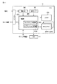
また、図3は、以上のようなシステム構成を持つ本コンピュータ1に起動ドライブとする外部記憶装置として搭載されるSSD12の概略構成を示すブロック図である。
FIG. 3 is a block diagram showing a schematic configuration of the
図示のように、SSD12は、温度センサ201、コネクタ202、制御部203、NANDメモリ204A〜204H、DRAM205、電源回路206等によって構成されており、電源が供給されなくても記憶が消えない(NANDメモリ204A〜204H上のプログラムを含むデータが失われない)不揮発性の外部記憶装置である。また、SSD12は、HDDのようにディスクやヘッド等の駆動機構を持たない、耐衝撃性の強い、低消費電力タイプの外部記憶装置である。
As shown in the figure, the
メモリコントローラとしてNANDメモリ204A〜204Hに対するデータの書き込みおよび読み出しを制御する制御部203は、コネクタ202、NANDメモリ204A〜204H、DRAM205、電源回路206にそれぞれ接続されている。本SSD12がコンピュータ本体2の内部に搭載された時、制御部203は、コネクタ202を介してホスト装置、即ちコンピュータ本体2のサウスブリッジ105と接続される。また、本SSD12が単体で存在する時には、制御部203は、必要に応じて、例えばRS−232C規格のシリアルインタフェースを介してデバッグ用機器と接続することができる。
A
また、図示のように、制御部203は、コンパクション処理部2031およびコンプレッション処理部2032を有しており、これらについては後述する。
As illustrated, the
NANDメモリ204A〜204Hは、各々が例えば16Gバイトの記憶容量をもつ不揮発性の半導体メモリであって、例えば1つのメモリセルに2ビットを記録可能なMLC(Multi Level Cell)−NANDメモリ(多値NANDメモリ)である。MLC−NANDメモリは、SLC(Single Level Cell)−NANDメモリに比較して、一般に書き換え可能回数は劣るが、記憶容量の大容量化は容易である。
Each of the
DRAM205は、制御部203によってNANDメモリ204A〜204Hに対するデータの書き込みおよび読み出しが行われる際に一時的にデータが格納されるキャッシュメモリとして利用されるメモリデバイスである。そして、電源回路206は、コネクタ202を介してサウスブリッジ105経由でEC/KBC107から供給される電力を電源として、制御部203の動作用の電力を生成・供給する。
The
図4は、本SSD12に設置されるNANDメモリ204A〜204Hの概略構成を示す概念図である。
FIG. 4 is a conceptual diagram showing a schematic configuration of
NANDメモリ204A〜204Hが構成する物理アドレス空間に対しては、物理的な使用最小単位とされるセクタa3として512バイトが定義され、また、データの管理単位とされるクラスタa2として8個分のセクタa3を纏めたデータサイズ、即ち、512バイト×8セクタ=4,096バイトが定義される。これに対して、本SSD12は、このNANDメモリ204A〜204Hの物理的なデータの書き込みおよび読み出し単位であるページサイズが4,314バイトを有している。つまり、本SSD12では、1つのページに1つのクラスタa2を格納し、各ページ毎に218バイトの冗長領域を設けるようにしている(4,314バイト−4,096バイト=218バイト)。なお、このページサイズの設定は単なる一例であり、1つのページに2以上のクラスタa2を格納するようにページサイズを設定することも当然に可能である。
For the physical address space formed by the NAND
また、NANDメモリ204A〜204Hは、独立して動作可能な複数のNANDブロックa1からそれぞれ構成されており、各NANDブロックa1は128ページで構成されている。つまり、1つのNANDグループa1には、128個のクラスタa2が格納される。そして、本SSD12では、16個のNANDブロックで1つのNANDグループを構成し、このNANDグループ(16×128=2,048クラスタ)単位で、データ消去を一括して行う等の記憶領域の管理を実行する。
Each of the
図5は、本SSD12の動作原理を説明するための概念図である。
FIG. 5 is a conceptual diagram for explaining the operation principle of the
図5に示すように、キャッシュメモリとして利用されるDRAM205上には、管理データ格納部2051、ライトキャッシュ2052およびリードキャッシュ2053が設けられる。一方、NANDメモリ204A〜204H上の各記憶領域は、管理データ領域2041、プライマリバッファ領域2042、メインストレージ領域2043、フリーグループ領域2044、コンパクションバッファ領域2045およびコンプレスドストレージ領域2046のいずれかとして動的に割り当てられる。
As shown in FIG. 5, a management
管理データ領域2041は、論理的なクラスタアドレス(LBA:Logical Block Address)と物理的なNANDメモリ204A〜204H上の位置とを対応づけるクラスタテーブルを格納する領域であり、制御部203は、本SSD12の起動時に、このクラスタテーブルをDRAM205上の管理データ格納部2051に取り込み、このDRAM205上のクラスタテーブルを使って、NANDメモリ204A〜204Hに対するアクセスを実行する。DRAM205上のクラスタテーブルは、例えば本SSD12の停止時などに発行される所定のコマンドを受けた際、NANDメモリ204A〜204H上に書き戻される。また、この管理データ格納部2051および管理データ領域2041には、プライマリバッファ領域2042内やコンパクションバッファ領域2045内における書き込み位置を示すポインタ情報なども格納される。
The
ホスト装置からデータの書き込みが要求されると、制御部203は、そのデータをDRAM205上のライトキャッシュ2052に一時的に蓄えながら、プライマリバッファ領域2042内の書き込み位置に書き込み、その書き込み位置と指定されたクラスタアドレスとを対応づけるべくDRAM205上のクラスタテーブルを更新する。もし、このデータの書き込みによって、プライマリバッファ領域2042として割り当てられているNANDグループが満杯になったならば、制御部203は、管理上、このNANDグループをメインストレージ領域2043に移行させ、フリーグループ領域2044として残存する未使用状態のNANDフリーグループの1つを新たにプライマリバッファ領域2042として割り当てる。
When data writing is requested from the host device, the
なお、本SSD12は、データを追記していくタイプの記憶装置であり、いわゆるデータの更新時には、更新前のデータを無効化し、更新後のデータを新たにプライマリバッファ領域2042内に書き込むことを内部的に実行する。つまり、例えばメインストレージ領域2043のNANDグループにおいてデータの置き換えが発生することはない。制御部203は、データの更新時、この更新前のデータの無効化および更新後のデータの新たな書き込みに伴うクラスタテーブルの更新を併せて実行する。
Note that the
一方、ホスト装置からデータの読み出しが要求されると、制御部203は、そのデータがDRAM205上のリードキャッシュ2053に存在しない場合、指定されたクラスタアドレスのNANDメモリ204A〜204H上における位置をDRAM205上のクラスタテーブルを参照して取得し、その位置に格納されたデータをリードキャッシュ2053に読み出して、ホスト装置に返却する。要求されたデータがリードキャッシュ2053に存在したならば、制御部203は、NANDメモリ204A〜204Hへのアクセスを行うことなく、そのデータを即座にホスト装置に返却する。
On the other hand, when data read is requested from the host device, the
以上のような流れでデータの書き込みおよびデータの読み出しを実行する本SSD12においては、データの書き込み効率を維持するために、フリーグループ領域2044として残存する未使用状態のNANDフリーグループの数を一定の水準以上に常時保っていることが好ましい。そのために、制御部203は、コンパクション処理部2031を備えている。NANDフリーグループの数が予め定められた値以下となった場合、制御部203は、コンパクション処理部2031によるコンパクションを実行する。
In the
コンパクション処理部2031は、まず、フリーグループ領域2044として残存する未使用状態のNANDフリーグループの1つをコンパクションバッファ領域2045として割り当てる。次に、コンパクション処理部2031は、メインストレージ領域2043のNANDグループの中から有効なデータ(有効クラスタ)の最も少ない、即ち、無効化されたデータ(無効化クラスタ)の最も多いNANDグループを選択し、その選択したNANDグループ内の有効クラスタのみをコンパクションバッファ領域2045に再配置していく。この有効クラスタの再配置に伴うクラスタテーブルの更新を、コンパクション処理部2031は併せて実行する。
First, the
選択したNANDグループ内のすべての有効クラスタを再配置し終えたら、このNANDグループをフリーグループ領域2044に返却する。続いて、2番目に有効クラスタの少ないNANDグループを選択して、同じく有効クラスタのみをコンパクションバッファ領域2045に再配置した後、フリーグループ領域2044に返却する。この処理を繰り返していき、もし、コンパクションバッファ領域2045として割り当てたNANDグループが満杯になったならば、コンパクション処理部2031は、このNANDグループをメインストレージ領域2043に移行させ、新たなNANDフリーグループを、コンパクションバッファ領域2045として割り当てる。例えば所定数のNANDフリーグループを新たに確保できた場合に、コンパクション処理部2031は、このコンパクションを終了する。
When all the valid clusters in the selected NAND group have been rearranged, this NAND group is returned to the
つまり、コンパクション処理部2031は、(最も無効化クラスタの多い順の)n個のNANDグループに点在する有効クラスタをn−1個以下のNANDグループに再配置することにより、最大n−1個のNANDフリーグループを確保する。
In other words, the
ところで、このコンパクションは、その実行そのものが、本SSD12におけるデータの書き込み効率を低下させる要因になり得る。よって、コンパクションの実行機会自体を抑えることができれば、よりデータの書き込み効率の維持を図ることが可能となる。そのために、制御部203は、さらにコンプレッション処理部2032を備える。
By the way, this compaction itself may be a factor of reducing the data writing efficiency in the
コンパクションの実行機会を抑えるためには、NANDフリーグループの数が予め定められた値以下になる状況を極力作らないことが求められる。そこで、制御部203は、例えば一定期間毎に、コンプレッション処理部2032によるデータ圧縮を実行する。
In order to suppress the execution opportunity of compaction, it is required not to create a situation where the number of NAND free groups is equal to or less than a predetermined value as much as possible. Therefore, the
コンプレッション処理部2032は、まず、フリーグループ領域2044として残存する未使用状態のNANDフリーグループの1つをコンプレスドストレージ領域2046として割り当てる。次に、コンプレッション処理部2032は、メインストレージ領域2043のNANDグループの中に、格納する有効データに対するアクセスが予め定められた期間を越えて行われていないNANDグループが存在しないかを検索する。この条件に合致するNANDグループが検出された場合、コンプレッション処理部2032は、もっとも最近アクセスされていない順にNANDグループの格納データを圧縮し、圧縮後の格納データをコンプレスドストレージ領域2046に再配置する。この再配置後、当該NANDグループはフリーグループ領域2044に返却される。
First, the
コンプレスドストレージ領域2046として割り当てたNANDグループが満杯になったならば、コンプレッション処理部2032は、新たなNANDフリーグループを、さらにコンプレスドストレージ領域2046として割り当てる。
When the NAND group allocated as the
仮に、圧縮後の格納データが約1/3のデータサイズに収まるならば、3つのNANDグループを1つのNANDグループに纏めて、2つのNANDグループをフリーグループ領域2044に返却することができる。どのようなデータが格納されているかによって圧縮の効果は左右されるので、コンプレッション処理部2032は、圧縮率の低いNANDグループをコンプレスドストレージ領域2046への移行対象から除外する。
If the stored data after compression fits into a data size of about 1/3, three NAND groups can be combined into one NAND group and the two NAND groups can be returned to the
つまり、コンプレッション処理部2032は、m個のNANDグループの格納データを圧縮してm−1個以下のNANDグループに再配置することにより、最大m−1個のNANDフリーグループを確保する。
That is, the
このコンプレッション処理部2032によるNANDフリーグループの確保より、コンパクションの実行機会を抑えることができ、よりデータの書き込み効率の維持を図ることが可能となる。
By securing the NAND free group by the
なお、格納データが圧縮されてコンプレスドストレージ領域2046に移されたNANDグループか否かを識別するための属性情報や、このコンプレスドストレージ領域2046内における書き込み位置を示すポインタ情報などは、DRAM205上の管理データ格納部2051によって保持され、NANDメモリ204A〜204Hの管理データ領域2041に適宜に反映される。
Note that attribute information for identifying whether or not the stored data is a NAND group that has been compressed and moved to the
コンプレッション処理部2032は、データを圧縮する機能に加えて、その圧縮したデータを解凍して復元する機能を併せて有しており、コンプレスドストレージ領域2046に移されたNANDグループ内の有効データに対する読み出し要求が発生すると、制御部203は、コンプレッション処理部2032により、当該NANDグループの格納データを解凍して復元し、読み出しが要求された有効データをDRAM205のリードキャッシュ2053に格納してホスト装置に返却する。
The
もし、このような手順で読み出される、コンプレスドストレージ領域2046に移されたNANDグループ内のデータに対する読み出し頻度(当該NANDグループ単位でのデータ読み出し頻度)が予め定められた値を越えた場合、制御部203は、コンプレッション処理部2032により、当該NANDグループの格納データを解凍して復元し、無効化クラスタを除いた有効クラスタすべてをコンパクションバッファ領域2045に再配置していく。コンパクションバッファ領域2045として割り当てたNANDグループは、満杯になった時点でメインストレージ領域2043に移されるので、この再配置によってコンプレスドストレージ領域2046からメインストレージ領域2043への効率的なデータ移行処理が実現される。
If the read frequency for the data in the NAND group transferred to the
また、コンプレスドストレージ領域2046に移されたNANDグループ内のデータの更新が発生すると、前述のように、データを追記していくタイプの記憶装置である本SSD12では、当該データを無効化して、更新後のデータを新たにプライマリバッファ領域2042内に書き込むことが内部的に実行される。そして、コンプレスドストレージ領域2046に移されたNANDグループ内の無効化データの容量が予め定められた値を越えた場合についても、制御部203は、コンプレッション処理部2032により、当該NANDグループの格納データを解凍して復元し、無効化クラスタを除いた有効クラスタすべてをコンパクションバッファ領域2045に再配置していく処理を実行する。この再配置によってNANDメモリ204A〜204Hの有効利用が図られる。
In addition, when the data in the NAND group moved to the
なお、コンプレスドストレージ領域2046に割り当てられたNANDグループは、その内部に(格納データが圧縮されて)移されてきたすべてのNANDグループの有効データがコンパクションバッファ領域2045に再配置された時点で、フリーグループ領域2044に返却される。
Note that the NAND group assigned to the
図6は、本SSD12の制御部203が実行するコンパクションによるフリーグループの確保の動作手順を示すフローチャートである。
FIG. 6 is a flowchart showing an operation procedure for securing a free group by compaction executed by the
制御部203は、フリーグループ領域2044として残存する未使用状態のNANDフリーグループの数が予め定められた値以下となった場合(ステップA1のYES)、メインストレージ領域2043のNANDグループの中から最も無効化クラスタが多い順にn個のNANDグループを選択し(ステップA2)、この選択したNANDグループに点在する有効クラスタをn−1個以下のNANDグループに再配置するコンパクションを実行して、最大n−1個のNANDフリーグループを確保する(ステップA3)。
When the number of unused NAND free groups remaining as the
図7は、本SSD12の制御部203が実行する圧縮によるフリーグループの確保の動作手順を示すフローチャートである。制御部203は、例えば一定期間毎に、この図9に示される処理を実行する。
FIG. 7 is a flowchart showing an operation procedure for securing a free group by compression executed by the
制御部203は、メインストレージ領域2043のNANDグループの中に予め定められた期間を越えてアクセスされていないNANDグループがm個以上存在する場合(ステップB1のYES)、最も最近アクセスされていない順にm個のNANDグループを選択し(ステップB2)、この選択したNANDグループの格納データを圧縮して、最大m−1個のNANDフリーグループを確保する(ステップB3)。
When there are m or more NAND groups that have not been accessed beyond a predetermined period in the NAND group in the main storage area 2043 (YES in step B1), the
また、図8は、本SSD12の制御部203が実行する圧縮データの読み出し処理の動作手順を示すフローチャートである。
FIG. 8 is a flowchart showing an operation procedure of compressed data read processing executed by the
圧縮された状態の有効データに対する読み出し要求が発生すると(ステップC1のYES)、制御部203は、このNANDグループの格納データを解凍し、DRAM205のリードキャッシュ2053上に読み出し対象データを展開する(ステップC2)。
When a read request for valid data in a compressed state is generated (YES in step C1), the
また、図9は、本SSD12の制御部203が実行する圧縮データの復元処理の動作手順を示すフローチャートである。
FIG. 9 is a flowchart showing the operation procedure of the compressed data decompression process executed by the
制御部203は、圧縮したNANDグループの中に、読み出し頻度が予め定められた値を越えたNANDグループが存在した場合(ステップD1のYES)、このNANDグループの格納データを解凍し、コンパクションバッファ領域2045に有効クラスタを再配置する(ステップD3)。また、制御部203は、圧縮したNANDグループの中に、無効化クラスタの数が予め定められた値を越えたNANDグループが存在した場合も(ステップD2のYES)、このNANDグループの格納データを解凍し、コンパクションバッファ領域2045に有効クラスタを再配置する(ステップD3)。
When there is a NAND group whose read frequency exceeds a predetermined value in the compressed NAND group (YES in step D1), the
以上のように、本SSD12においては、長期間アクセスされないデータを圧縮して空き記憶領域を確保することにより、コンパクションの発生を抑えて、書き込み効率を維持することを実現する。
As described above, in the
なお、本発明は、上記実施形態そのままに限定されるものではなく、実施段階ではその要旨を逸脱しない範囲で構成要素を変形して具体化できる。また、上記実施形態に開示されている複数の構成要素の適宜な組み合わせにより種々の発明を形成できる。例えば、実施形態に示される全構成要素から幾つかの構成要素を削除してもよい。更に、異なる実施形態に構成要素を適宜組み合わせてもよい。 Note that the present invention is not limited to the above-described embodiment as it is, and can be embodied by modifying the constituent elements without departing from the scope of the invention in the implementation stage. In addition, various inventions can be formed by appropriately combining a plurality of components disclosed in the embodiment. For example, some components may be deleted from all the components shown in the embodiment. Furthermore, you may combine a component suitably in different embodiment.
1…パーソナルコンピュータ、2…コンピュータ本体、3…ディスプレイユニット、4…LCD、5…電源スイッチ、6…キーボード、7…タッチパッド、8…LED、9…ODD、10…PCカードスロット、11…USBコネクタ、12…SSD、101…CPU、102…ノースブリッジ、103…メインメモリ、104…GPU、105…サウスブリッジ、106…フラッシュメモリ、107…EC/KBC、108…ファン、201…温度センサ、202…コネクタ、203…制御部、204A〜204H…NANDメモリ、205…DRAM、206…電源回路、2031…コンパクション処理部、2032…コンプレッション処理部、2041…管理データ領域、2042…プライマリバッファ領域、2043…メインストレージ領域、2044…フリーグループ領域、2045…コンパクションバッファ領域、2046…コンプレスドストレージ領域、2051…管理データ格納部、2052…ライトキャッシュ、2053…リードキャッシュ。
DESCRIPTION OF
Claims (7)
前記不揮発性半導体メモリに対するデータの書き込みおよび読み出しを制御するコントローラと、
を具備し、
前記コントローラは、
前記不揮発性半導体メモリ上における記憶領域の管理単位として構成される複数のグループ中に残存する、未使用状態にあるフリーグループの数が予め定められた数以下となった場合に、n個のグループ上に点在する有効データをn−1個以下のグループ上に再配置することによってフリーグループを確保するコンパクション制御手段と、
格納する有効データに対するアクセスが予め定められた期間を越えて行われていないm個のグループ上の格納データを圧縮してm−1個以下のグループ上に再配置することによってフリーグループを確保するコンプレッション制御手段と、
を有することを特徴とする不揮発性半導体メモリドライブ装置。 Non-volatile semiconductor memory;
A controller that controls writing and reading of data to and from the nonvolatile semiconductor memory;
Comprising
The controller is
When the number of free groups remaining in a plurality of groups configured as storage unit management units on the nonvolatile semiconductor memory is equal to or less than a predetermined number, n groups Compaction control means for securing a free group by rearranging the effective data scattered above on n-1 or less groups;
A free group is secured by compressing stored data on m groups that have not been accessed for valid data to be stored for a predetermined period of time and rearranging them on groups of m−1 or less. Compression control means;
A non-volatile semiconductor memory drive device comprising:
前記コントローラの前記コンプレッション制御手段は、格納データが圧縮されて他のグループの格納データと共に再配置されている状態にあるグループ上の有効データの読み出しが要求された場合、その格納データを解凍して当該読み出しが要求された有効データを前記キャッシュメモリ上に格納する、
ことを特徴とする請求項1記載の不揮発性半導体メモリドライブ装置。 A cache memory,
The compression control means of the controller decompresses the stored data when it is requested to read valid data on the group in which the stored data is compressed and rearranged together with the stored data of another group. Storing the valid data requested to be read in the cache memory;
The nonvolatile semiconductor memory drive device according to claim 1.
不揮発性半導体メモリを搭載する不揮発性半導体メモリドライブ装置と、
を具備し、
前記本体装置は、前記不揮発性半導体メモリに対するデータアクセス要求を不揮発性半導体メモリドライブ装置に発行するデータアクセス要求手段を有し、
前記不揮発性半導体メモリドライブ装置は、前記不揮発性半導体メモリに対するデータの書き込みおよび読み出しを制御するコントローラを有し、
前記不揮発性半導体メモリドライブ装置の前記コントローラは、
前記不揮発性半導体メモリ上における記憶領域の管理単位として構成される複数のグループ中に残存する、未使用状態にあるフリーグループの数が予め定められた数以下となった場合に、n個のグループ上に点在する有効データをn−1個以下のグループ上に再配置することによってフリーグループを確保するコンパクション制御手段と、
格納する有効データに対するアクセスが予め定められた期間を越えて行われていないm個のグループ上の格納データを圧縮してm−1個以下のグループ上に再配置することによってフリーグループを確保するコンプレッション制御手段と、
前記コンパクション制御手段による再配置または前記コンプレッション制御手段による再配置の実行中、前記不揮発性半導体メモリに対するデータアクセス要求が前記本体装置から発行された場合、前記コンパクション制御手段による再配置または前記コンプレッション制御手段による再配置の実行を中断させる制御手段と、
を含むことを特徴とする情報処理装置。 A main unit,
A nonvolatile semiconductor memory drive device including a nonvolatile semiconductor memory;
Comprising
The main unit has data access request means for issuing a data access request to the nonvolatile semiconductor memory to the nonvolatile semiconductor memory drive device,
The nonvolatile semiconductor memory drive device has a controller that controls writing and reading of data to and from the nonvolatile semiconductor memory,
The controller of the nonvolatile semiconductor memory drive device includes:
When the number of free groups remaining in a plurality of groups configured as storage unit management units on the nonvolatile semiconductor memory is equal to or less than a predetermined number, n groups Compaction control means for securing a free group by rearranging the effective data scattered above on n-1 or less groups;
A free group is secured by compressing stored data on m groups that have not been accessed for valid data to be stored for a predetermined period of time and rearranging them on groups of m−1 or less. Compression control means;
When a data access request for the nonvolatile semiconductor memory is issued from the main unit during execution of relocation by the compaction control means or relocation by the compression control means, relocation by the compaction control means or the compression control means Control means for interrupting execution of relocation by
An information processing apparatus comprising:
前記コントローラが、
前記不揮発性半導体メモリ上における記憶領域の管理単位として構成される複数のグループ中に残存する、未使用状態にあるフリーグループの数が予め定められた数以下となった場合に、n個のグループ上に点在する有効データをn−1個以下のグループ上に再配置することによってフリーグループを確保するステップと、
格納する有効データに対するアクセスが予め定められた期間を越えて行われていないm個のグループ上の格納データを圧縮してm−1個以下のグループ上に再配置することによってフリーグループを確保するステップと、
を具備することを特徴とする記憶領域の管理方法。 A method for managing a storage area in a nonvolatile semiconductor memory drive device, comprising: a nonvolatile semiconductor memory; and a controller that controls writing and reading of data to and from the nonvolatile semiconductor memory,
The controller is
When the number of free groups remaining in a plurality of groups configured as storage unit management units on the nonvolatile semiconductor memory is equal to or less than a predetermined number, n groups Securing a free group by relocating valid data scattered above on n-1 or fewer groups;
A free group is secured by compressing stored data on m groups that have not been accessed for valid data to be stored for a predetermined period of time and rearranging them on groups of m−1 or less. Steps,
A storage area management method comprising:
Priority Applications (3)
| Application Number | Priority Date | Filing Date | Title |
|---|---|---|---|
| JP2008328073A JP4461187B1 (en) | 2008-12-24 | 2008-12-24 | Nonvolatile semiconductor memory drive device, information processing device, and storage area management method in nonvolatile semiconductor memory drive device |
| US12/546,532 US8135902B2 (en) | 2008-12-24 | 2009-08-24 | Nonvolatile semiconductor memory drive, information processing apparatus and management method of storage area in nonvolatile semiconductor memory drive |
| JP2010024153A JP2010152909A (en) | 2008-12-24 | 2010-02-05 | Nonvolatile semiconductor memory drive device, information management device, management method of storage area in nonvolatile semiconductor memory drive device |
Applications Claiming Priority (2)
| Application Number | Priority Date | Filing Date | Title |
|---|---|---|---|
| JP2008328073A JP4461187B1 (en) | 2008-12-24 | 2008-12-24 | Nonvolatile semiconductor memory drive device, information processing device, and storage area management method in nonvolatile semiconductor memory drive device |
| JP2010024153A JP2010152909A (en) | 2008-12-24 | 2010-02-05 | Nonvolatile semiconductor memory drive device, information management device, management method of storage area in nonvolatile semiconductor memory drive device |
Related Child Applications (1)
| Application Number | Title | Priority Date | Filing Date |
|---|---|---|---|
| JP2010024153A Division JP2010152909A (en) | 2008-12-24 | 2010-02-05 | Nonvolatile semiconductor memory drive device, information management device, management method of storage area in nonvolatile semiconductor memory drive device |
Publications (2)
| Publication Number | Publication Date |
|---|---|
| JP4461187B1 true JP4461187B1 (en) | 2010-05-12 |
| JP2010152516A JP2010152516A (en) | 2010-07-08 |
Family
ID=61026349
Family Applications (2)
| Application Number | Title | Priority Date | Filing Date |
|---|---|---|---|
| JP2008328073A Expired - Fee Related JP4461187B1 (en) | 2008-12-24 | 2008-12-24 | Nonvolatile semiconductor memory drive device, information processing device, and storage area management method in nonvolatile semiconductor memory drive device |
| JP2010024153A Pending JP2010152909A (en) | 2008-12-24 | 2010-02-05 | Nonvolatile semiconductor memory drive device, information management device, management method of storage area in nonvolatile semiconductor memory drive device |
Family Applications After (1)
| Application Number | Title | Priority Date | Filing Date |
|---|---|---|---|
| JP2010024153A Pending JP2010152909A (en) | 2008-12-24 | 2010-02-05 | Nonvolatile semiconductor memory drive device, information management device, management method of storage area in nonvolatile semiconductor memory drive device |
Country Status (2)
| Country | Link |
|---|---|
| US (1) | US8135902B2 (en) |
| JP (2) | JP4461187B1 (en) |
Cited By (1)
| Publication number | Priority date | Publication date | Assignee | Title |
|---|---|---|---|---|
| TWI746101B (en) * | 2020-08-03 | 2021-11-11 | 宏碁股份有限公司 | Electronic device and thermal controlling method for solid state disk thereof |
Families Citing this family (22)
| Publication number | Priority date | Publication date | Assignee | Title |
|---|---|---|---|---|
| US20110004728A1 (en) * | 2009-07-02 | 2011-01-06 | Ocz Technology Group, Inc. | On-device data compression for non-volatile memory-based mass storage devices |
| KR101090407B1 (en) * | 2009-12-24 | 2011-12-06 | 주식회사 팍스디스크 | Control Method of Semiconductor Storage System Managing Dual Memory Regions |
| KR101649357B1 (en) * | 2010-05-10 | 2016-08-19 | 삼성전자주식회사 | Data storage device, operating method thereof, and storage server including the same |
| WO2012039002A1 (en) * | 2010-09-21 | 2012-03-29 | Hitachi, Ltd. | Semiconductor storage device and data control method thereof |
| JP5066241B2 (en) * | 2010-09-24 | 2012-11-07 | 株式会社東芝 | Memory system |
| US9311229B2 (en) * | 2011-03-29 | 2016-04-12 | Blackberry Limited | System and method for managing flash memory |
| JP6045567B2 (en) * | 2011-04-26 | 2016-12-14 | シーゲイト テクノロジー エルエルシーSeagate Technology LLC | Variable over-provisioning for non-volatile storage |
| US8782370B2 (en) * | 2011-05-15 | 2014-07-15 | Apple Inc. | Selective data storage in LSB and MSB pages |
| JP5674634B2 (en) | 2011-12-28 | 2015-02-25 | 株式会社東芝 | Controller, storage device and program |
| JP5687639B2 (en) | 2012-02-08 | 2015-03-18 | 株式会社東芝 | Controller, data storage device and program |
| US20140032820A1 (en) * | 2012-07-25 | 2014-01-30 | Akinori Harasawa | Data storage apparatus, memory control method and electronic device with data storage apparatus |
| JP2014052899A (en) | 2012-09-07 | 2014-03-20 | Toshiba Corp | Memory system and control method of the same |
| US20140281129A1 (en) * | 2013-03-15 | 2014-09-18 | Tal Heller | Data tag sharing from host to storage systems |
| KR102078853B1 (en) | 2013-11-27 | 2020-02-18 | 삼성전자 주식회사 | Memory system, host system and method for performing write operation in memory system |
| US9606870B1 (en) * | 2014-03-31 | 2017-03-28 | EMC IP Holding Company LLC | Data reduction techniques in a flash-based key/value cluster storage |
| US10025843B1 (en) | 2014-09-24 | 2018-07-17 | EMC IP Holding Company LLC | Adjusting consistency groups during asynchronous replication |
| US10360144B2 (en) | 2015-02-27 | 2019-07-23 | Hitachi, Ltd. | Storage apparatus and non-volatile memory device including a controller to selectively compress data based on an update frequency level |
| JP6414852B2 (en) * | 2015-12-14 | 2018-10-31 | 東芝メモリ株式会社 | Memory system and control method |
| US10152527B1 (en) | 2015-12-28 | 2018-12-11 | EMC IP Holding Company LLC | Increment resynchronization in hash-based replication |
| JP2018160194A (en) | 2017-03-23 | 2018-10-11 | 東芝メモリ株式会社 | Memory system and method |
| US10691354B1 (en) | 2018-01-31 | 2020-06-23 | EMC IP Holding Company LLC | Method and system of disk access pattern selection for content based storage RAID system |
| JP2020198128A (en) * | 2020-08-31 | 2020-12-10 | キオクシア株式会社 | Memory system |
Citations (4)
| Publication number | Priority date | Publication date | Assignee | Title |
|---|---|---|---|---|
| JPH06202921A (en) * | 1992-10-22 | 1994-07-22 | Nec Corp | File compression processor |
| JPH08249159A (en) * | 1995-03-09 | 1996-09-27 | Fujitsu Ltd | Disk controller |
| JPH09128276A (en) * | 1995-08-28 | 1997-05-16 | Toshiba Corp | Computer system and file managing method used by the same |
| JP2003044351A (en) * | 2001-07-27 | 2003-02-14 | Matsushita Electric Ind Co Ltd | Flash memory device and method for merging data stored in the same |
Family Cites Families (16)
| Publication number | Priority date | Publication date | Assignee | Title |
|---|---|---|---|---|
| JPH03195988A (en) | 1989-12-25 | 1991-08-27 | Marine Instr Co Ltd | Echo-sounding machine |
| GB2251323B (en) | 1990-12-31 | 1994-10-12 | Intel Corp | Disk emulation for a non-volatile semiconductor memory |
| JPH04312092A (en) * | 1991-04-11 | 1992-11-04 | Sony Corp | Digital transmission test signal generating circuit |
| AU679457B2 (en) * | 1992-10-22 | 1997-07-03 | Nec Corporation | File compression processor |
| JP3641280B2 (en) | 1992-10-30 | 2005-04-20 | インテル・コーポレーション | Method for determining blocks to be cleaned up in a flash EEPROM array |
| WO1996037846A1 (en) * | 1995-05-22 | 1996-11-28 | Syncronys Softcorp | Virtual memory management system with adaptive knowledge base |
| JPH09231109A (en) | 1996-02-27 | 1997-09-05 | Nec Corp | File device |
| US5860124A (en) * | 1996-09-30 | 1999-01-12 | Intel Corporation | Method for performing a continuous over-write of a file in nonvolatile memory |
| US6775751B2 (en) * | 2002-08-06 | 2004-08-10 | International Business Machines Corporation | System and method for using a compressed main memory based on degree of compressibility |
| TWI227409B (en) | 2003-06-05 | 2005-02-01 | Carry Computer Eng Co Ltd | Storage device capable of enhancing transmission speed |
| JP4534590B2 (en) | 2004-05-14 | 2010-09-01 | 栗田工業株式会社 | Solid oxide fuel cell |
| WO2007019198A2 (en) * | 2005-08-03 | 2007-02-15 | Sandisk Corporation | Non-volatile memory with scheduled reclaim operations |
| JP4939084B2 (en) | 2006-03-10 | 2012-05-23 | 富士フイルム株式会社 | Catalyst material for fuel cell, production method thereof, catalyst membrane, electrode membrane assembly, and fuel cell |
| JP5037952B2 (en) | 2007-01-15 | 2012-10-03 | 株式会社日立製作所 | Storage system and storage system control method |
| US9183133B2 (en) * | 2007-11-28 | 2015-11-10 | Seagate Technology Llc | System, method, and computer program product for increasing spare space in memory to extend a lifetime of the memory |
| US20090172248A1 (en) * | 2007-12-27 | 2009-07-02 | Guangqing You | Management of a flash memory device |
-
2008
- 2008-12-24 JP JP2008328073A patent/JP4461187B1/en not_active Expired - Fee Related
-
2009
- 2009-08-24 US US12/546,532 patent/US8135902B2/en active Active
-
2010
- 2010-02-05 JP JP2010024153A patent/JP2010152909A/en active Pending
Patent Citations (4)
| Publication number | Priority date | Publication date | Assignee | Title |
|---|---|---|---|---|
| JPH06202921A (en) * | 1992-10-22 | 1994-07-22 | Nec Corp | File compression processor |
| JPH08249159A (en) * | 1995-03-09 | 1996-09-27 | Fujitsu Ltd | Disk controller |
| JPH09128276A (en) * | 1995-08-28 | 1997-05-16 | Toshiba Corp | Computer system and file managing method used by the same |
| JP2003044351A (en) * | 2001-07-27 | 2003-02-14 | Matsushita Electric Ind Co Ltd | Flash memory device and method for merging data stored in the same |
Cited By (1)
| Publication number | Priority date | Publication date | Assignee | Title |
|---|---|---|---|---|
| TWI746101B (en) * | 2020-08-03 | 2021-11-11 | 宏碁股份有限公司 | Electronic device and thermal controlling method for solid state disk thereof |
Also Published As
| Publication number | Publication date |
|---|---|
| JP2010152516A (en) | 2010-07-08 |
| JP2010152909A (en) | 2010-07-08 |
| US8135902B2 (en) | 2012-03-13 |
| US20100161884A1 (en) | 2010-06-24 |
Similar Documents
| Publication | Publication Date | Title |
|---|---|---|
| JP4461187B1 (en) | Nonvolatile semiconductor memory drive device, information processing device, and storage area management method in nonvolatile semiconductor memory drive device | |
| JP4439578B1 (en) | Nonvolatile semiconductor memory drive device and data management method for nonvolatile semiconductor memory drive device | |
| JP5349897B2 (en) | Storage system | |
| US10776153B2 (en) | Information processing device and system capable of preventing loss of user data | |
| US10884630B2 (en) | Storage system | |
| JP6045567B2 (en) | Variable over-provisioning for non-volatile storage | |
| EP2942713B1 (en) | Storage system and storage apparatus | |
| US8130554B1 (en) | Securely erasing flash-based memory | |
| US10222984B1 (en) | Managing multi-granularity flash translation layers in solid state drives | |
| US10146435B2 (en) | Storage system and data write method | |
| US20140189203A1 (en) | Storage apparatus and storage control method | |
| US20110099323A1 (en) | Non-volatile semiconductor memory segregating sequential, random, and system data to reduce garbage collection for page based mapping | |
| KR20060123573A (en) | Dual media storage | |
| JP2013196115A (en) | Memory system | |
| US11061814B1 (en) | Managing data storage caching and tiering | |
| KR20130024271A (en) | Storage system including hdd and nvm | |
| US20080263282A1 (en) | System for Caching Data | |
| KR20190061426A (en) | Flash memory system and control method thereof | |
| KR20130079706A (en) | Method of operating storage device including volatile memory | |
| US10891057B1 (en) | Optimizing flash device write operations | |
| JP2012038212A (en) | Storage device and control method thereof | |
| JP5025670B2 (en) | Information processing apparatus and data storage apparatus | |
| JP5694212B2 (en) | Management information generation method and memory system | |
| JP2010152517A (en) | Nonvolatile semiconductor memory drive device and address management method for the same | |
| Ji et al. | Locality and duplication-aware garbage collection for flash memory-based virtual memory systems |
Legal Events
| Date | Code | Title | Description |
|---|---|---|---|
| TRDD | Decision of grant or rejection written | ||
| A01 | Written decision to grant a patent or to grant a registration (utility model) |
Free format text: JAPANESE INTERMEDIATE CODE: A01 Effective date: 20100119 |
|
| A01 | Written decision to grant a patent or to grant a registration (utility model) |
Free format text: JAPANESE INTERMEDIATE CODE: A01 |
|
| A61 | First payment of annual fees (during grant procedure) |
Free format text: JAPANESE INTERMEDIATE CODE: A61 Effective date: 20100215 |
|
| R151 | Written notification of patent or utility model registration |
Ref document number: 4461187 Country of ref document: JP Free format text: JAPANESE INTERMEDIATE CODE: R151 |
|
| FPAY | Renewal fee payment (event date is renewal date of database) |
Free format text: PAYMENT UNTIL: 20130219 Year of fee payment: 3 |
|
| FPAY | Renewal fee payment (event date is renewal date of database) |
Free format text: PAYMENT UNTIL: 20140219 Year of fee payment: 4 |
|
| S111 | Request for change of ownership or part of ownership |
Free format text: JAPANESE INTERMEDIATE CODE: R313111 |
|
| R350 | Written notification of registration of transfer |
Free format text: JAPANESE INTERMEDIATE CODE: R350 |
|
| LAPS | Cancellation because of no payment of annual fees |