JP4440284B2 - Low pressure plasma processing apparatus and method - Google Patents
Low pressure plasma processing apparatus and method Download PDFInfo
- Publication number
- JP4440284B2 JP4440284B2 JP2007123072A JP2007123072A JP4440284B2 JP 4440284 B2 JP4440284 B2 JP 4440284B2 JP 2007123072 A JP2007123072 A JP 2007123072A JP 2007123072 A JP2007123072 A JP 2007123072A JP 4440284 B2 JP4440284 B2 JP 4440284B2
- Authority
- JP
- Japan
- Prior art keywords
- substrate
- chamber
- film substrate
- plasma
- plasma processing
- Prior art date
- Legal status (The legal status is an assumption and is not a legal conclusion. Google has not performed a legal analysis and makes no representation as to the accuracy of the status listed.)
- Expired - Fee Related
Links
- 238000012545 processing Methods 0.000 title claims description 124
- 238000000034 method Methods 0.000 title claims description 21
- 239000000758 substrate Substances 0.000 claims description 439
- 238000012546 transfer Methods 0.000 claims description 54
- 238000001179 sorption measurement Methods 0.000 claims description 29
- 239000007789 gas Substances 0.000 claims description 28
- 238000009832 plasma treatment Methods 0.000 claims description 25
- 238000002360 preparation method Methods 0.000 claims description 25
- 238000011068 loading method Methods 0.000 claims description 19
- 238000004140 cleaning Methods 0.000 claims description 11
- 239000012495 reaction gas Substances 0.000 claims description 8
- 239000000126 substance Substances 0.000 claims description 6
- 238000007664 blowing Methods 0.000 claims description 5
- IJGRMHOSHXDMSA-UHFFFAOYSA-N Atomic nitrogen Chemical compound N#N IJGRMHOSHXDMSA-UHFFFAOYSA-N 0.000 description 17
- 238000007689 inspection Methods 0.000 description 13
- 230000008569 process Effects 0.000 description 13
- MYMOFIZGZYHOMD-UHFFFAOYSA-N Dioxygen Chemical compound O=O MYMOFIZGZYHOMD-UHFFFAOYSA-N 0.000 description 12
- 229910001882 dioxygen Inorganic materials 0.000 description 12
- 238000010926 purge Methods 0.000 description 10
- 229910001873 dinitrogen Inorganic materials 0.000 description 9
- 239000000498 cooling water Substances 0.000 description 8
- 238000000605 extraction Methods 0.000 description 8
- 238000004891 communication Methods 0.000 description 6
- 229910052760 oxygen Inorganic materials 0.000 description 6
- 239000001301 oxygen Substances 0.000 description 5
- 230000009471 action Effects 0.000 description 4
- 239000000853 adhesive Substances 0.000 description 4
- 230000001070 adhesive effect Effects 0.000 description 4
- QVGXLLKOCUKJST-UHFFFAOYSA-N atomic oxygen Chemical compound [O] QVGXLLKOCUKJST-UHFFFAOYSA-N 0.000 description 4
- 238000011109 contamination Methods 0.000 description 4
- 230000000694 effects Effects 0.000 description 4
- 230000004048 modification Effects 0.000 description 4
- 238000012986 modification Methods 0.000 description 4
- 229910052757 nitrogen Inorganic materials 0.000 description 4
- 238000001816 cooling Methods 0.000 description 3
- XLYOFNOQVPJJNP-UHFFFAOYSA-N water Substances O XLYOFNOQVPJJNP-UHFFFAOYSA-N 0.000 description 3
- CURLTUGMZLYLDI-UHFFFAOYSA-N Carbon dioxide Chemical compound O=C=O CURLTUGMZLYLDI-UHFFFAOYSA-N 0.000 description 2
- ZAMOUSCENKQFHK-UHFFFAOYSA-N Chlorine atom Chemical compound [Cl] ZAMOUSCENKQFHK-UHFFFAOYSA-N 0.000 description 2
- 230000005856 abnormality Effects 0.000 description 2
- 230000004913 activation Effects 0.000 description 2
- 229910052786 argon Inorganic materials 0.000 description 2
- -1 argon ions Chemical class 0.000 description 2
- 230000033228 biological regulation Effects 0.000 description 2
- 125000003178 carboxy group Chemical group [H]OC(*)=O 0.000 description 2
- 230000008859 change Effects 0.000 description 2
- 239000000460 chlorine Substances 0.000 description 2
- 229910052801 chlorine Inorganic materials 0.000 description 2
- 239000000356 contaminant Substances 0.000 description 2
- 230000001276 controlling effect Effects 0.000 description 2
- 239000012212 insulator Substances 0.000 description 2
- 238000005304 joining Methods 0.000 description 2
- 238000004519 manufacturing process Methods 0.000 description 2
- 230000007246 mechanism Effects 0.000 description 2
- 230000006641 stabilisation Effects 0.000 description 2
- 238000011105 stabilization Methods 0.000 description 2
- 230000002159 abnormal effect Effects 0.000 description 1
- PNEYBMLMFCGWSK-UHFFFAOYSA-N aluminium oxide Inorganic materials [O-2].[O-2].[O-2].[Al+3].[Al+3] PNEYBMLMFCGWSK-UHFFFAOYSA-N 0.000 description 1
- XKRFYHLGVUSROY-UHFFFAOYSA-N argon Substances [Ar] XKRFYHLGVUSROY-UHFFFAOYSA-N 0.000 description 1
- 239000012298 atmosphere Substances 0.000 description 1
- 238000010923 batch production Methods 0.000 description 1
- 125000004432 carbon atom Chemical group C* 0.000 description 1
- 229910002092 carbon dioxide Inorganic materials 0.000 description 1
- 239000001569 carbon dioxide Substances 0.000 description 1
- 125000002915 carbonyl group Chemical group [*:2]C([*:1])=O 0.000 description 1
- 238000009833 condensation Methods 0.000 description 1
- 230000005494 condensation Effects 0.000 description 1
- 238000010586 diagram Methods 0.000 description 1
- 239000000428 dust Substances 0.000 description 1
- 238000005516 engineering process Methods 0.000 description 1
- 230000006870 function Effects 0.000 description 1
- 230000006872 improvement Effects 0.000 description 1
- 239000011810 insulating material Substances 0.000 description 1
- 238000009413 insulation Methods 0.000 description 1
- 238000002715 modification method Methods 0.000 description 1
- 239000012299 nitrogen atmosphere Substances 0.000 description 1
- 239000005416 organic matter Substances 0.000 description 1
- 239000010453 quartz Substances 0.000 description 1
- 230000009467 reduction Effects 0.000 description 1
- 230000001105 regulatory effect Effects 0.000 description 1
- 239000011347 resin Substances 0.000 description 1
- 229920005989 resin Polymers 0.000 description 1
- 238000007789 sealing Methods 0.000 description 1
- VYPSYNLAJGMNEJ-UHFFFAOYSA-N silicon dioxide Inorganic materials O=[Si]=O VYPSYNLAJGMNEJ-UHFFFAOYSA-N 0.000 description 1
- 238000004544 sputter deposition Methods 0.000 description 1
- 238000012360 testing method Methods 0.000 description 1
Images


Landscapes
- Manufacturing Of Printed Wiring (AREA)
- Plasma Technology (AREA)
Description
本発明は、被処理基板の表面を処理するプラズマを減圧雰囲気下で発生させるプラズマ処理装置に関するものである。 The present invention relates to a plasma processing apparatus that generates plasma for processing the surface of a substrate to be processed in a reduced pressure atmosphere.
実装技術の分野において、電子機器の小型化・高機能化に伴い高密度な実装が要求されている。そのため、実装基板への素子の接続は微細化され、より信頼性の高い実装が必要とされている。信頼性を確保する方法の一つとしてプラズマによる表面改質方法がある。たとえば、このプラズマ処理によって、表面に付着した有機物汚染が除去され、ワイヤーボンディングのボンディング強度を向上したり、濡れ性が改善され、基板と封止樹脂との密着性を向上することができる。すなわち、酸素プラズマにより基板表面の活性化を起こし、カルボキシル基(COO)、カルボニル基(C=O)などができて、接合強度の向上につながるといった表面活性化作用を生じさせる。また、アルゴンイオン又は酸素イオンによるスパッタリング作用により、表面洗浄作用を生じさせる。 In the field of mounting technology, high-density mounting is required as electronic devices become smaller and more functional. For this reason, the connection of the element to the mounting substrate is miniaturized, and more reliable mounting is required. One method for ensuring reliability is a surface modification method using plasma. For example, this plasma treatment can remove organic contaminants attached to the surface, improve the bonding strength of wire bonding, improve the wettability, and improve the adhesion between the substrate and the sealing resin. That is, activation of the substrate surface is caused by oxygen plasma, and carboxyl groups (COO), carbonyl groups (C = O), and the like are generated, thereby causing a surface activation action that leads to improvement in bonding strength. Further, a surface cleaning action is generated by a sputtering action by argon ions or oxygen ions.
特に、フィルムなどから構成されるフレキシブル回路基板において基板表面に塩素が残っていると、基板周囲の湿気と反応したり、回路を流れる電流などの影響で回路が腐食する可能性があるため、プラズマ処理によって、表面に付着した塩素が除去されるようにしている。 In particular, if chlorine remains on the substrate surface in a flexible circuit board made of film, etc., it may react with the moisture around the substrate or the circuit may corrode due to the current flowing through the circuit. The treatment removes chlorine adhering to the surface.
このようなプラズマ処理の従来の構成としては、フィルムを数枚ずつ人の手でチャンバー内に載置し、チャンバー蓋を閉じてから、真空粗引き、本引き、ガスバルブ開、高周波電力印加、高周波電力印加停止、大気圧復帰、チャンバー開の一連の動作を人が1つずつ行う。真空圧の確認は真空計によって行い、高周波電力印加時間はストップウォッチで計測する。 As a conventional configuration of such plasma processing, several films are placed in a chamber by hand by hand, the chamber lid is closed, vacuum roughing, main drawing, gas valve opening, high frequency power application, high frequency power A person performs a series of operations of stopping power application, returning to atmospheric pressure, and opening the chamber one by one. The vacuum pressure is confirmed with a vacuum gauge, and the high frequency power application time is measured with a stopwatch.
しかしながら、上記構造のものでは、必然的にバッチ処理になるために、スループットに限界がある。また、人の手によってフィルムを出し入れする為に、フィルムが汚染される可能性がある。さらに、洗浄と次工程の間にブランクが発生する為に、フィルムの管理が難しい。 However, in the above structure, since it is necessarily a batch process, the throughput is limited. Further, since the film is taken in and out by a human hand, the film may be contaminated. Furthermore, since blanks are generated between the cleaning and the next process, it is difficult to manage the film.
従って、本発明の目的は、上記問題を解決することにあって、スループットを向上させることができ、フィルム汚染が効果的に防止でき、フィルムの管理が容易に行うことができる減圧プラズマ処理装置及びその方法を提供することにある。 Accordingly, an object of the present invention is to solve the above-described problems, and it is possible to improve the throughput, effectively prevent film contamination, and manage the film easily. It is to provide such a method.
上記目的を達成するために、本発明は以下のように構成する。 In order to achieve the above object, the present invention is configured as follows.
本発明の第1態様によれば、プラズマ処理装置本体外の基板搬入準備位置と上記プラズマ処理装置本体内の基板搬入位置との間でフィルム基板を移動させる基板搬入スライダと、
上記プラズマ処理装置本体内の基板搬出準備位置と上記プラズマ処理装置本体外の基板搬出位置との間で上記フィルム基板を移動させる基板搬出スライダと、
上記プラズマ処理装置本体内に配置され、上記フィルム基板を静電吸着により吸着保持する基板電極を備え、その内部を排気しつつ反応ガスを導入して減圧下で高周波電力を上記基板電極に印加してプラズマを発生させて上記フィルム基板から有機物を除去するプラズマ処理が上記内部にて行われるチャンバーと、
上記基板搬入位置に移動された上記フィルム基板を吸着保持するノズルを有し、そのノズルにより吸着保持された上記フィルム基板を上記チャンバーの上記基板電極に移動させる、基板搬入用の第1搬送アーム装置と、
上記プラズマ処理された上記フィルム基板を吸着保持するノズルを有し、そのノズルにより吸着保持された上記フィルム基板を上記チャンバーの上記基板電極から上記基板搬送準備位置に移動させる、基板搬出用の第2搬送アーム装置と、
を備えた減圧プラズマ処理装置であって、
上記基板電極への静電チャック電圧の印加を開始し所定の電圧値に安定した後、上記第1搬送アーム装置のノズルによる上記フィルム基板の吸着保持を解除するとともにブローすることにより上記第1搬送アーム装置のノズルから上記基板電極に上記フィルム基板を受け渡すように制御するとともに、
上記基板電極への静電チャック電圧の印加を停止し始めると同時に、上記第2搬送アーム装置のノズルによる上記プラズマ処理されたフィルム基板の吸着保持を開始することにより上記基板電極から上記第2搬送アーム装置のノズルに上記プラズマ処理されたフィルム基板を受け渡すように制御する制御手段
を備えることを特徴とする減圧プラズマ処理装置を提供する。
According to the first aspect of the present invention, a substrate loading slider for moving the film substrate between a substrate loading preparation position outside the plasma processing apparatus main body and a substrate loading position within the plasma processing apparatus main body,
A substrate unloading slider for moving the film substrate between a substrate unloading preparation position in the plasma processing apparatus main body and a substrate unloading position outside the plasma processing apparatus main body;
A substrate electrode disposed in the plasma processing apparatus main body and holding the film substrate by electrostatic adsorption is introduced. A reactive gas is introduced while exhausting the inside of the film substrate, and high-frequency power is applied to the substrate electrode under reduced pressure. A chamber in which plasma treatment is performed to generate plasma and remove organic substances from the film substrate;
A first transfer arm device for carrying a substrate having a nozzle for sucking and holding the film substrate moved to the substrate carry-in position and moving the film substrate sucked and held by the nozzle to the substrate electrode of the chamber When,
A second substrate for carrying out the substrate having a nozzle for sucking and holding the plasma-treated film substrate and moving the film substrate sucked and held by the nozzle from the substrate electrode of the chamber to the substrate transport preparation position; A transfer arm device;
A low-pressure plasma processing apparatus comprising:
After the application of the electrostatic chuck voltage to the substrate electrode is started and stabilized to a predetermined voltage value, the suction of the film substrate by the nozzle of the first transport arm device is released and the first transport is performed by blowing. While controlling to deliver the film substrate from the nozzle of the arm device to the substrate electrode,
At the same time as the application of the electrostatic chuck voltage to the substrate electrode starts to be stopped, the second transport arm device starts to suck and hold the plasma-treated film substrate by the nozzle of the second transport arm device, thereby starting the second transport from the substrate electrode. There is provided a reduced-pressure plasma processing apparatus comprising control means for controlling to deliver the plasma-treated film substrate to a nozzle of an arm apparatus.
本発明の第2態様によれば、フィルム基板をプラズマ処理装置本体外から上記プラズマ処理装置本体内の基板搬入位置に搬入し、
上記基板搬入位置に位置した上記フィルム基板を、基板搬入用の第1搬送アーム装置に備えられたノズルにより吸着保持した状態でチャンバー内の基板電極に搬入し、
上記チャンバー内を排気しつつ反応ガスを導入して減圧下で高周波電力を静電吸着により上記フィルム基板を吸着保持した上記基板電極に印加してプラズマを発生させて上記フィルム基板から有機物を除去するプラズマ処理を行い、
上記基板電極に静電吸着保持され上記プラズマ処理された上記フィルム基板を、基板搬出用の第2搬送アーム装置に備えられたノズルにより吸着保持して上記チャンバーから取り出して上記プラズマ処理装置本体内の基板搬出準備位置に位置させ、
上記基板搬出準備位置に位置した上記フィルム基板を上記プラズマ処理装置本体外に搬出するようにした減圧プラズマ洗浄方法であって、
上記チャンバー内の上記基板電極に搬入するとき、上記基板電極への静電チャック電圧の印加を開始し所定の電圧値に安定した後、上記第1搬送アーム装置のノズルによる上記フィルム基板の吸着保持を解除するとともにブローすることにより上記第1搬送アーム装置のノズルから上記基板電極に上記フィルム基板を受け渡すとともに、
上記チャンバーから上記プラズマ処理された上記フィルム基板を取り出すとき、上記基板電極への静電チャック電圧の印加を停止し始めると同時に、上記第2搬送アーム装置のノズルによる上記プラズマ処理されたフィルム基板の吸着保持を開始することにより上記基板電極から上記第2搬送アーム装置のノズルに上記プラズマ処理されたフィルム基板を受け渡すようにしたことを特徴とする減圧プラズマ洗浄方法を提供する。
According to the second aspect of the present invention, the film substrate is carried from the outside of the plasma processing apparatus main body to the substrate carrying position in the plasma processing apparatus main body,
The film substrate located on the substrate loading position, and carried into a substrate electrode in the chamber while more attracted and held by the first nozzle provided in the transfer arm device for substrate loading,
The reaction gas is introduced while evacuating the chamber, and high-frequency power is applied to the substrate electrode holding the film substrate by electrostatic adsorption under reduced pressure to generate plasma to remove organic substances from the film substrate. Perform plasma treatment,
The film substrate which is the plasma treatment is held electrostatically attracted to the substrate electrode, and more attracted and held by the second nozzle provided in the transfer arm device for the substrate carry-out is removed from the chamber the plasma processing apparatus main body Located at the board unloading preparation position,
A reduced-pressure plasma cleaning method in which the film substrate positioned at the substrate unloading preparation position is unloaded from the plasma processing apparatus main body ,
When the substrate electrode in the chamber is carried in, the application of the electrostatic chuck voltage to the substrate electrode is started and stabilized at a predetermined voltage value, and then the film substrate is sucked and held by the nozzle of the first transfer arm device. The film substrate is transferred from the nozzle of the first transfer arm device to the substrate electrode by releasing and blowing,
When the plasma-treated film substrate is taken out of the chamber, the application of the electrostatic chuck voltage to the substrate electrode starts to be stopped, and at the same time, the plasma-treated film substrate by the nozzle of the second transfer arm device There is provided a reduced-pressure plasma cleaning method characterized in that the plasma-treated film substrate is delivered from the substrate electrode to the nozzle of the second transfer arm device by starting adsorption holding .
本発明によれば、フィルム基板をプラズマ処理装置本体外からプラズマ処理装置本体内の基板搬入位置に搬入し、上記基板搬入位置に位置した上記フィルム基板をチャンバー内に搬入し、上記チャンバー内を排気しつつ反応ガスを導入して減圧下で高周波電力を印加してプラズマを発生させて上記フィルム基板から有機物を除去するプラズマ処理を行い、上記プラズマ処理されたフィルム基板を上記チャンバーから取り出して上記プラズマ処理装置本体内の基板搬出準備位置に位置させ、上記基板搬出準備位置に位置した上記フィルム基板を上記プラズマ処理装置本体外に搬出するようにしている。従って、フィルム基板毎に、搬入、プラズマ処理、搬出動作をそれぞれ独立して自動的に行うことができ、フィルム基板の減圧プラズマ洗浄処理を全自動化することによって人の介在を無くし、フィルム基板の実装工程におけるインライン化が可能となる。 According to the present invention, the film substrate is carried from the outside of the plasma processing apparatus main body to the substrate carrying-in position in the plasma processing apparatus main body, the film substrate positioned at the substrate carrying-in position is carried into the chamber, and the inside of the chamber is evacuated. The plasma treatment is performed to remove the organic substances from the film substrate by introducing a reactive gas and applying high-frequency power under reduced pressure to generate plasma and removing the plasma-treated film substrate from the chamber. The film substrate positioned at the substrate unloading preparation position is positioned inside the processing apparatus main body, and the film substrate positioned at the substrate unloading preparation position is unloaded from the plasma processing apparatus main body. Therefore, loading, plasma processing, and unloading operations can be performed automatically and independently for each film substrate, eliminating the need for human intervention by fully automating the reduced pressure plasma cleaning processing of the film substrate, and mounting the film substrate. In-line in the process becomes possible.
また、減圧プラズマ洗浄処理を全自動化することができて、スループットを向上させることができ、フィルム基板の汚染が効果的に防止でき、フィルム基板の管理が容易に行うことができる。 In addition, the reduced-pressure plasma cleaning process can be fully automated, throughput can be improved, contamination of the film substrate can be effectively prevented, and management of the film substrate can be easily performed.
また、チャンバーでの基板電極に対するフィルム基板の保持を静電吸着により行うようにすれば、フィルム基板の形状が異なっても基板電極を交換する必要はなく、フィルム基板の品種切り替え時の基板電極の交換ロスを削減することができる。また、チャンバー内にフィルム基板保持ジグも不要とすることができる。 In addition, if the film substrate is held against the substrate electrode in the chamber by electrostatic adsorption, it is not necessary to replace the substrate electrode even if the shape of the film substrate is different. Exchange loss can be reduced. Further, a film substrate holding jig can be dispensed with in the chamber.
以下に、本発明にかかる実施の形態を図面に基づいて詳細に説明する。 Embodiments according to the present invention will be described below in detail with reference to the drawings.
本発明の第1の実施形態にかかるプラズマ処理装置は、図1(A),(B)に示すように、フィルム基板2などの回路基板をチャンバー8内の基板電極8b上に自動的に搬入し、チャンバー8内を排気しかつ所定の反応ガスをチャンバー8内に導入して所定の減圧状態を維持した上で、高周波電源8cから高周波電力を印加してチャンバー8内に酸素プラズマを発生させ、発生した酸素プラズマにより、基板電極8b上に保持した基板2の表面をプラズマ処理して、基板2の表面の有機物の炭素原子と酸素を結合させて二酸化炭素の気相として基板2の表面から有機物を自動的に除去して、ICチップや部品などを接合するための基板電極などの接合部の表面を活性化させて接合力を強化できるようにするものである。
The plasma processing apparatus according to the first embodiment of the present invention automatically carries a circuit board such as a
具体的には、プラズマ処理装置は、図2及び図11〜図13に示すように、一対のフィルム基板2,2を保持してプラズマ処理装置本体10外からプラズマ処理装置本体10内に搬入する基板搬入スライダ1と、基板搬入スライダ1から一対のフィルム基板2,2を吸着保持しかつ移動する一対の搬送アーム装置3A,3Bと、一対の搬送アーム装置3A,3Bが固定されて支持されかつ一対の搬送アーム装置3A,3Bを基板搬送方向(図2の左方向、図15参照)F沿いに移動させる移動装置4と、一対のフィルム基板2,2のプラズマ処理を行う第1チャンバー8Aと一対のフィルム基板2,2のプラズマ処理を行う第2チャンバー8Bとを有するプラズマ処理チャンバー8と、一対のフィルム基板2,2を保持してプラズマ処理装置本体10内からプラズマ処理装置本体10外に搬出する基板搬出スライダ9とを備えている。
Specifically, as shown in FIGS. 2 and 11 to 13, the plasma processing apparatus holds a pair of
上記基板搬入スライダ1は、プラズマ処理装置本体10外の基板搬入準備位置Aと、プラズマ処理装置本体10内の基板搬入位置Bとの間で、一対のフィルム基板2,2を吸着保持しつつ、モータ又はエアシリンダなどの駆動装置の駆動により移動する。
The substrate carry-in
上記移動装置4は、一対の搬送アーム装置3A,3Bが移動体4a上に固定されて支持され、移動体4aは、サーボモータ4cなどの駆動装置によりガイド部材4bに沿って基板搬送方向F沿いに往復移動可能となっている。
In the
一対の搬送アーム装置3A,3Bのそれぞれは、移動体4aに固定されたモータなどのアーム部駆動装置6aと、モータなどの駆動装置6aの駆動により軸方向(基板搬送方向Fと直交する方向)に移動するアーム部6と、アーム部6の先端に配置されかつ吸着部昇降装置7aにより上下動可能に一対の吸着部7,7とを備えて、吸着部昇降装置7aの駆動により一対の吸着部7,7を下端位置まで下降させて、図示しない吸引装置の駆動により、一対のフィルム基板2,2を同時的に一対の吸着部7,7で吸着保持可能としている。また、移動体4aの近傍側の基板搬入スライダ1又は基板搬出スライダ9と各チャンバー8との間でアーム部駆動装置6aの駆動により一対の吸着部7,7が移動可能として両装置間で一対のフィルム基板2,2を同時的に受け渡し可能としている。
Each of the pair of
一方の(図2では右側のすなわち基板搬入側に近い側の)搬送アーム装置3Aはチャンバー8A,8Bにフィルム基板2,2を搬入する搬送アーム装置である。他方の(図2では左側のすなわち基板搬出側に近い側の)搬送アーム装置3Bは、チャンバー8A,8Bからフィルム基板2,2を搬出する搬送アーム装置である。従って、それぞれの搬送アーム装置は、プラズマ処理前のフィルム基板2,2又はプラズマ処理後のフィルム基板2,2を常に吸着することになり、プラズマ処理前と後の両方の状態のフィルム基板2,2を同じ搬送アーム装置で吸着しないため、吸着による汚染を無くすことができる。
One
上記基板搬出スライダ9は、プラズマ処理装置本体10外の基板搬出準備位置Cと、プラズマ処理装置本体10内の基板搬出位置Dとの間で、一対のフィルム基板2,2を吸着保持しつつ、モータ又はエアシリンダなどの駆動装置の駆動により移動する。なお、一対のフィルム基板2,2の保持の方法は、吸着に限らず、他の手段、例えば、係止部材などで保持できるようにしてもよい。
The substrate carry-out
第1チャンバー8Aは、一対のフィルム基板2,2が一対の第1搬送アーム装置3Aにより搬入して蓋8aを閉じたのち、排気され減圧されてArと酸素ガスなどの反応ガスが導入されたのち、高周波電力が印加されて第1チャンバー8A内にプラズマを発生させて、一対のフィルム基板2,2の各表面がプラズマ処理される。その後、大気圧に戻したのち、蓋8aを開けて、一対のフィルム基板2,2が第2搬送アーム装置3Bにより搬出する。
In the
第2チャンバー8Bは、一対のフィルム基板2,2が一対の第1搬送アーム装置3Aにより搬入して蓋8aを閉じたのち、減圧されて反応ガスが導入されたのち、高周波が印加されてプラズマを発生させて、一対のフィルム基板2,2の各表面がプラズマ処理される。その後、大気圧に戻したのち蓋8aを開けて、一対のフィルム基板2,2が第2搬送アーム装置3Bにより搬出する。
In the
第1チャンバー8Aと第2チャンバー8Bとは、それぞれ独立してプラズマ処理を行うことができる。よって、例えば、一方のチャンバーでプラズマ処理を行っているときに、他方のチャンバーでプラズマ処理が終了したフィルム基板2を搬出し、次にプラズマ処理を行うフィルム基板2を搬入させることができる。なお、蓋8aは蓋開閉用エアシリンダ30の駆動によりそれぞれ開閉される。
The
第1チャンバー8A及び第2チャンバー8Bは同一構成であり、そのチャンバー8を図3に示す。図3において、8aは上下方向にスライドして開閉するチャンバー8の蓋、8eはチャンバー8の側壁内面に配置された石英のカバー、8gは基板静電吸着用のDC電極と高周波電力が印加される基板電極8b本体とを絶縁する絶縁材、8hは基板電極8bを冷却する冷却水流路、8iは冷却水流路に冷却水を供給する冷却水用配管、8kは基板電極8bとチャンバー8とを絶縁するためのアルミナなどから構成されるインシュレータ、8mはSUS304などから構成されるチャンバー8の側壁、8nはSUS304などから構成されるチャンバー8のベース、8pは基板静電吸着用のDC電源8tに接続された基板静電吸着用のDC電極、8qは基板電極8bの冷却水流路を形成するためのSUS304などから構成される水冷ジャケット、8rは高周波電源8cに接続された高周波印加電極である。なお、チャンバー8の側壁8m、ベース8n、蓋8aはアースされている。従って、フィルム基板2は、各チャンバー8内の基板電極8b上に載置されると、基板静電吸着用のDC電源8tからDC電圧が基板静電吸着用のDC電極8pに印加されて、フィルム基板2が静電吸着作用により基板電極8b上に吸着保持される。プラズマ処理中、フィルム基板2はこのように静電吸着された状態で保持され、プラズマ処理終了後、取り出すときには、基板静電吸着用のDC電極8pへのDC電圧の印加を停止又は逆方向に電圧を作用させて、フィルム基板2が基板電極8b上から取出しやすくする。
The
これを図4〜図7に基いて詳細に説明する。 This will be described in detail with reference to FIGS.
図4及び図5に示すように、吸着部7から基板電極8bにフィルム基板2を受け渡すとき、フィルム基板2を吸着保持した吸着部7を吸着部昇降装置7aにより下端位置まで下降させて、フィルム基板2を基板電極8bの直上に位置させる。この状態で、静電吸着用のDC電圧を基板電極8bに印加開始し、所定の電圧値に安定したのち、吸着部7によるフィルム基板2の吸着保持を解除するとともにブローを行い、吸着部7から確実にフィルム基板2を分離すると同時に、静電吸着力により、フィルム基板2を基板電極8bに静電吸着する。このようにすることにより、フィルム基板2に無理な力が作用することなく、円滑に、吸着部7から基板電極8bにフィルム基板2を受け渡すことができる。
As shown in FIGS. 4 and 5, when the
一方、逆に、図6及び図7に示すように、基板電極8bから吸着部7にフィルム基板2を受け渡すとき、吸着部7を吸着部昇降装置7aにより下端位置まで下降させて、吸着部7を基板電極8bに静電吸着されたフィルム基板2の直上に位置させる。この状態で、静電吸着用のDC電圧の印加を停止し始めると同時に、吸着部7によるフィルム基板2の吸着保持を開始して、吸着部7によりフィルム基板2を吸着保持する。なお、基板電極8bには、静電吸着用のDC電圧の逆電圧を印加して、フィルム基板2が基板電極8bから確実に分離されるようにしている。このようにすることにより、フィルム基板2に無理な力が作用することなく、円滑に、基板電極8bから吸着部7にフィルム基板2を受け渡すことができる。
On the other hand, as shown in FIGS. 6 and 7, when the
次に、各チャンバー8A,8Bに関する配管系及び排気ガス供給などのプラズマ処理動作について図8及び図9及び図29を参照しながら説明する。
Next, the plasma processing operation such as the piping system and the exhaust gas supply for the
図8及び図9及び図29において、Rpは両チャンバー8A,8B用の排気ポンプ、Mvは排気ポンプRpによる排気動作における制御弁、Cvは上記排気動作における流量調整弁であり、粗引き後に所定の減圧状態を維持するように制御弁Mvと流量調整弁Cvとで圧力調整を行うようにしている。SRv及びRvはそれぞれ上記排気動作に対するスローラフ(粗引き)動作制御バルブ及びラフ(粗引き)動作制御バルブ、Sv1は上記排気動作に対する第1チャンバー用オンオフ弁、Sv2は上記排気動作に対する第2チャンバー用オンオフ弁、Gは各チャンバー内の圧力を計測する真空計である。また、SHvは開閉弁として機能しかつ第1チャンバー8Aと第2チャンバー8Bとを連通管60で直結して減圧状態から大気圧状態への復帰を促進する直結弁(ショート弁)、Pv1及びPv2は第1チャンバー8Aと第2チャンバー8Bとへ切り換えで窒素ガスを供給可能とする窒素ガス用の切換弁である。また、SGv1及びSGv2は第1チャンバー8Aと第2チャンバー8Bとへ切り換えでArガス又は酸素ガスなどを供給可能とする切換弁、Gv1,Gv2,Gv3はそれぞれArガス用、酸素ガス用、予備用のオンオフ弁、MFCはArガス用、酸素ガス用、予備用の流量調整弁である。図9において、RFは高周波電源、SET L1は第2チャンバー8Bの大気圧セットポイント、SET L2は第2チャンバー8Bのスロー排気圧セットポイント、PLは第2チャンバー8Bの圧力である。また、SET R1は第1チャンバー8Aの大気圧セットポイント、SET R2は第1チャンバー8Aのスロー排気圧セットポイント、PRは第1チャンバー8Aの圧力である。また、P1は粗引き終了を意味するメインバルブのオン圧力(Pa)、P2はバックグランド圧力(Pa)、P3はプラズマ処理圧力(Pa)である。また、T1はプラズマ処理時間(s)、T2はガス排気時間(s)、T3は余分にパージして蓋8aを開けやすくするためのパージ安定時間(s)、T4は両チャンバー8A,8Bを連通するショート時間(s)を示す。
8, 9 and 29, Rp is an exhaust pump for both
従って、第1チャンバー8Aで排気動作を行うときには上記第1チャンバー用オンオフ弁Sv1を開けておく。第2チャンバー8Bで排気動作を行うときには上記第2チャンバー用オンオフ弁Sv2を開けておく。この実施形態では、いずれか一方のオンオフ弁Svを開け、同時に2つのオンオフ弁Svは開けないが、これに限られるものではない。そして、排気ポンプRpが駆動されて排気動作を開始するとき、図9及び図28に示すように、最初はスローラフ(粗引き)動作を行わせるようにスローラフ(粗引き)動作制御バルブSRvを開け、排気動作すべき第1又は第2チャンバー8A又は8Bの真空計Gの圧力がSET R2又はSET L2になると、ラフ(粗引き)動作制御バルブRvを開く。このようにすることにより、排気ポンプRpであるロータリーポンプへの急激な空気の流入を防ぎ、オイルの飛散やポンプの損傷を防ぐといった効果がある。
そして、第1又は第2チャンバー8A又は8Bの真空計Gにより第1又は第2チャンバー8A又は8Bの圧力PR又はPLがメインバルブオン圧力P1になると、その後、制御弁Mvと流量調整弁Cvとにより減圧状態を制御して、第1又は第2チャンバー8A又は8Bの圧力PR又はPLがバックグランド圧力P2となったのち、Arガス用の流量調整弁MFCとArガス用オンオフ弁Gv1、酸素ガス用の流量調整弁MFCと酸素ガス用オンオフ弁Gv2、予備用の流量調整弁MFCと予備用のオンオフ弁Gv3を適宜動作させて、所望のガスを所定の減圧状態となったチャンバー8へ供給可能した上で、切換弁SGv1又はSGv2を切り換えて、Arガス又は酸素ガスなどを上記所定の減圧状態となったチャンバー8へ供給する。
Therefore, when the exhaust operation is performed in the
When the pressure PR or PL of the first or
このArガス又は酸素ガスなどの供給後、ガス導入動作が安定化したのち、高周波電力を基板電極8bに印加してプラズマをチャンバー8内に発生させてフィルム基板2,2の電極などの接合部のプラズマ処理を行う。所定のプラズマ処理時間T1だけプラズマ処理を行ったのち、Arガス又は酸素ガスなどの供給を停止してガス排気時間T2の間、排気する。その後、窒素ガス用の切換弁Pv1又はPv2を切り換えて、窒素ガスを所定の減圧状態となったチャンバー8へ供給して窒素パージを行う。このとき、窒素パージ開始時に、第1チャンバー8Aと第2チャンバー8Bとを連通する連通管60の直結弁SHvを開けて、プラズマ処理を行っていたチャンバー8A又は8Bと、蓋8aを閉じてプラズマ処理用の排気動作を開始した直後のチャンバー8B又は8Aとを連通させることにより、プラズマ処理を行っていたチャンバー8A又は8Bの減圧状態を迅速に同気圧状態に戻すことができる(なお、蓋8aを開けてのフィルム基板2,2のチャンバー8への搬入環境は窒素雰囲気であるため、プラズマ処理を行っていたチャンバー8A又は8Bでの窒素パージ動作に何ら支障は生じない。)。
上記したプラズマ処理装置は、基板搬入スライダ1、搬送アーム装置3A,B、移動装置4、第1チャンバー8A、第2チャンバー8B、各高周波電源8c、各基板静電吸着用のDC電源、基板搬出スライダ9などがコントローラ20に接続されて、コントローラ20によりそれぞれの動作が制御されている。
After the Ar gas or oxygen gas is supplied, the gas introduction operation is stabilized, and then high frequency power is applied to the
The plasma processing apparatus described above includes the substrate carry-in
また、部品実装基板の製造ライン内での上記プラズマ処理装置の配置の一例を図14に示す。図14において、41は多数のフィルム基板2,…,2が収納され一枚ずつ基板搬送方向F沿いに送り出すローダ、40はフィルム基板2を2枚毎に上記プラズマ処理する上記プラズマ処理装置、42は上記プラズマ処理された各フィルム基板2にACF(異方性導電フィルム)を介してICチップを実装するICボンダ、43は各フィルム基板2の所定個所に接着剤を塗布する接着剤塗布装置、44は各フィルム基板2の接着剤が塗布された上記所定個所などに部品を実装する部品実装装置、45はフィルム基板2同士を接着して製品化するFPCボンダ、46は送られてきた製品を検査する検査装置、47は基板搬送方向F沿いに一個ずつ送られてきた製品を収納するアンローダである。
FIG. 14 shows an example of the arrangement of the plasma processing apparatus in the component mounting board production line. In FIG. 14,
上記プラズマ処理装置の作用について図2、図15〜図22、図23を参照しながら詳細に説明する。 The operation of the plasma processing apparatus will be described in detail with reference to FIGS. 2, 15 to 22, and 23.
図15に示すように、基板搬入スライダ1に一対のフィルム基板2,2すなわち2−1,2−2が載置されているとする。一対のフィルム基板2−1,2−2を載置した基板搬入スライダ1が基板搬入準備位置Aから基板搬入位置Bに移動して停止する(丸1参照)。
As shown in FIG. 15, it is assumed that a pair of
次に、移動装置4により基板搬送方向F沿いに移動(丸2参照)して、一対の搬送アーム装置3A,3Bのうちの第1搬送アーム装置3Aの一対の吸着部7,7が基板搬入位置Bに位置した基板搬入スライダ1上の一対のフィルム基板2−1,2−2に向けて下降し、同時的に吸着保持したのち、上昇する(丸3参照)。
Next, the moving
次いで、移動装置4により基板搬送方向F沿いに次の動作位置まで移動するとともに(丸4参照)、プラズマ処理が終了した第2チャンバー8Bの蓋8aが開かれる(丸5参照)。なお、第2チャンバー8B内でプラズマ処理された一対のフィルム基板2,2が既にある場合には、一対の搬送アーム装置3A,3Bのうちの第2搬送アーム装置3Bの一対の吸着部7,7により、プラズマ処理された一対のフィルム基板2,2が吸着保持されて第2チャンバー8Bから取り出される(丸6参照)。この動作の前に、基板搬出スライダ9は基板搬出位置Dから基板搬出準備位置Cに戻っている(丸7参照)。また、基板搬入スライダ1は、基板搬入位置Bから基板搬入準備位置Aに戻って、次の新しいフィルム基板2−3,2−4を載置したのち、基板搬入位置Bに戻る(丸8参照及び図17参照)。
Next, the moving
その後、移動装置4により基板搬送方向F沿いに移動したのち(丸9参照)、第1搬送アーム装置3Aが基板搬入スライダ1の上方から、蓋8aが開かれた第2チャンバー8B内に臨む上方位置まで移動して、第1搬送アーム装置3Aの一対の吸着部7,7が第2チャンバー8Bの上方位置から下降して、図16に示すように第2チャンバー8B内の基板電極8bに一対のフィルム基板2−1,2−2を載置したのち、上昇し、初期位置まで戻る((10)参照)。第2チャンバー8Bでは、一対のフィルム基板2−1,2−2が基板電極8bに載置されたのち、蓋8aを閉じて((11)参照)第2チャンバー8B内を排気して105Paから1Paに減圧にするとともに、所定の反応ガスを1Paから10Paになるまで流入させて、10Paの所定の圧力状態を維持して高周波電力が印加されてプラズマが発生させられてプラズマ処理が行われる。プラズマ処理後、窒素ガスが流入されて、20Paから105Paとなり、第2チャンバー8Bの蓋8aが開かれる(丸5参照)。
After that, after moving along the substrate transport direction F by the moving device 4 (see circle 9), the first
一方、移動装置4により基板搬送方向F沿いにさらに移動したのち((12)参照)、一対の搬送アーム装置3A,3Bのうちの第2搬送アーム装置3Bの一対の吸着部7,7に吸着保持していたプラズマ処理済みの一対のフィルム基板2,2を、基板搬入位置Bに位置した基板搬入スライダ1上に載置する((13)参照)。その後、基板搬出スライダ9は、その上に一対のフィルム基板2,2が載置されたのち、基板搬出準備位置Cから基板搬出位置Dに移動する((14)参照)。
On the other hand, after further moving along the substrate transfer direction F by the moving device 4 (see (12)), the two
次いで、移動装置4により基板搬送方向Fとは反対方向沿いに移動したのち((15)参照)、図17に示すように、一対の搬送アーム装置3A,3Bのうちの第1搬送アーム装置3Aの一対の吸着部7,7が基板搬入位置Bに位置した基板搬入スライダ1上の一対のフィルム基板2−2,2−3に向けて下降し、同時的に吸着保持したのち、上昇する((16)参照)。
Next, after moving along the direction opposite to the substrate transport direction F by the moving device 4 (see (15)), as shown in FIG. 17, the first
次いで、移動装置4により基板搬送方向F沿いに次の動作位置まで移動するとともに((17)参照)、プラズマ処理が終了した第1チャンバー8Aの蓋8aが開かれる((18)参照)。なお、第1チャンバー8A内でプラズマ処理された一対のフィルム基板2,2が既にある場合には、一対の搬送アーム装置3A,3Bのうちの第2搬送アーム装置3Bの一対の吸着部7,7により、プラズマ処理された一対のフィルム基板2,2が吸着保持されて第1チャンバー8Aから取り出される((19)参照)。この動作の前に、基板搬出スライダ9は基板搬出位置Dから基板搬出準備位置Cに戻っている((14)参照)。また、基板搬入スライダ1は、基板搬入位置Bから基板搬入準備位置Aに戻って、次の新しいフィルム基板2,2を載置したのち、基板搬入位置Bに戻る((1)参照)。
Next, the moving
その後、移動装置4により基板搬送方向F沿いに移動したのち((20)参照)、第1搬送アーム装置3Aが基板搬入スライダ1の上方から、蓋8aが開かれた第1チャンバー8A内に臨む上方位置まで移動して、第1搬送アーム装置3Aの一対の吸着部7,7が第1チャンバー8Aの上方位置から下降して、図18に示すように第1チャンバー8A内の基板電極8bに一対のフィルム基板2−3,2−4を載置したのち、上昇し、初期位置まで戻る((21)参照)。第1チャンバー8Aでは、一対のフィルム基板2−3,2−4が基板電極8bに載置されたのち、蓋8aを閉じて((22)参照)第1チャンバー8A内を排気して105Paから1Paに減圧にするとともに、所定の反応ガスを1Paから10Paになるまで流入させて、10Paの所定の圧力状態を維持して高周波電力が印加されてプラズマが発生させられてプラズマ処理が行われる。プラズマ処理後、窒素ガスが流入されて、20Paから105Paとなり、第1チャンバー8Aの蓋8aが開かれる((18)参照)。
Then, after moving along the substrate transport direction F by the moving device 4 (see (20)), the first
一方、移動装置4により基板搬送方向F沿いにさらに移動したのち((23)参照)、図18に示すように、一対の搬送アーム装置3A,3Bのうちの第2搬送アーム装置3Bの一対の吸着部7,7に吸着保持していたプラズマ処理済みの一対のフィルム基板2−1,2−2を、基板搬出準備位置Cに位置した基板搬出スライダ9上に載置する((25)参照)。その後、基板搬出スライダ9は、その上に一対のフィルム基板2,2が載置されたのち、基板搬出準備位置Cから基板搬出位置Dに移動する(丸7参照)。その後、図23に示すように、上記動作を繰り返す。
On the other hand, after further moving along the substrate transfer direction F by the moving device 4 (see (23)), as shown in FIG. 18, the pair of second
なお、上記プラズマ処理装置とこれに隣接配置されるICボンダ42との関係について主として説明する。
The relationship between the plasma processing apparatus and the
次いで、図19に示すように、基板搬出位置Dに位置した基板搬出スライダ9の一対のフィルム基板2−1,2−2のうちの一方のフィルム基板2−1を取り出して、下流側に隣接する部品実装装置例えばICボンダ42の基板供給取出し位置Iに搬入させる。
Next, as shown in FIG. 19, one film substrate 2-1 of the pair of film substrates 2-1 and 2-2 of the
次いで、図20に示すように、ICボンダ42の基板保持装置42aを90度間欠的に回転させて、基板供給取出し位置Iに供給されたフィルム基板2−1をACF貼り付け位置IIに位置させてACF(異方性導電フィルム)をフィルム基板2−1に貼り付け開始する。このとき同時に、基板搬出位置Dに位置した基板搬出スライダ9の一対のフィルム基板2−1,2−2のうちの残りのフィルム基板2−2を取り出して、下流側に隣接するICボンダ42の基板供給取出し位置Iに搬入させる。この動作の間、第1チャンバー8Aでの一対のフィルム基板2−3,2−4のプラズマ処理が終了し、第2搬送アーム装置3Bの一対の吸着部7,7により、一対のフィルム基板2−1,2−2を、第1チャンバー8Aから取り出して基板搬出準備位置Cに位置した基板搬出スライダ9上に載置する。
Next, as shown in FIG. 20, the
次いで、図21に示すように、ICボンダ42の基板保持装置42aを90度間欠的にさらに回転させて、ACF貼り付け位置IIに位置されたフィルム基板2−1を検査位置IIIに位置させて検査を開始すると同時に、基板供給取出し位置Iに供給されたフィルム基板2−2をACF貼り付け位置IIに位置させてACFをフィルム基板2−2に貼り付け開始する。このとき同時に、基板搬出位置Dに位置した基板搬出スライダ9の一対のフィルム基板2−3,2−4のうちの一方のフィルム基板2−3を取り出して、下流側に隣接するICボンダ42の基板供給取出し位置Iに搬入させる。
Next, as shown in FIG. 21, the
次いで、図22に示すように、ICボンダ42の基板保持装置42aを90度間欠的にさらに回転させて、検査位置IIIに位置されたフィルム基板2−1をIC装着位置IVに位置させてICチップをACFを介してフィルム基板2−1に装着し、ACF貼り付け位置IIに位置されたフィルム基板2−2を検査位置IIIに位置させて検査を開始すると同時に、基板供給取出し位置Iに供給されたフィルム基板2−3をACF貼り付け位置IIに位置させてACFをフィルム基板2−3に貼り付け開始する。このとき同時に、基板搬出位置Dに位置した基板搬出スライダ9の一対のフィルム基板2−3,2−4のうちの残りのフィルム基板2−4を取り出して、下流側に隣接するICボンダ42の基板供給取出し位置Iに搬入させる。なお、この後、ICボンダ42の基板保持装置42aを90度間欠的にさらに回転させられて、ICチップがACFを介して装着されたフィルム基板2−1が基板供給取出し位置Iに位置すると、フィルム基板2−1が基板保持装置42aから取り出されて次の工程に搬送される一方、次にICチップを装着すべきフィルム基板2が基板供給取出し位置Iに搬入される。
Next, as shown in FIG. 22, the
以降、上記した動作が繰り返されて、フィルム基板2,…,2のプラズマ処理、及び、プラズマ処理後のACFを介してのICチップ実装処理が自動的に連続して行われる。
Thereafter, the above operation is repeated, and the plasma processing of the
一例として、プラズマ処理条件を以下に記載する。 As an example, plasma processing conditions are described below.
プラズマ処理変更条件としては、酸素ガス流量は0〜20sccm、Arガス流量は0〜20sccm、高周波電力は0〜300W、真空度は10〜100Pa、ガス導入系は図示したように3系統(一例として、Arガスは50sccm、酸素ガスは50sccm、予備ガスは50sccm、)とする。直結用の連通管60は1系統とする。
As conditions for changing the plasma treatment, the oxygen gas flow rate is 0 to 20 sccm, the Ar gas flow rate is 0 to 20 sccm, the high frequency power is 0 to 300 W, the degree of vacuum is 10 to 100 Pa, and the gas introduction system is three systems (as an example) , Ar gas is 50 sccm, oxygen gas is 50 sccm, and reserve gas is 50 sccm). The
真空排気系は、排気ポンプRpの一例としてロータリーポンプを使用し、図8のCvである手動コンダクタンスバルブ(自動排気制御バルブAPCでもよい。)を使用する。 The vacuum exhaust system uses a rotary pump as an example of the exhaust pump Rp, and uses a manual conductance valve (which may be an automatic exhaust control valve APC) which is Cv in FIG.
到達真空度の一例としては、9Pa以下とする。 As an example of the ultimate vacuum, it is 9 Pa or less.
基板電極用の冷却水の流量は15リットル/min、圧力は1127.8〜294.2kPa(11.5〜3kgf/cm2)(背圧無きこと)、水温は15〜30℃(結露しないように室温以上が良い。)とする。 The flow rate of cooling water for the substrate electrode is 15 liters / min, the pressure is 1127.8 to 294.2 kPa (11.5 to 3 kgf / cm 2 ) (no back pressure), and the water temperature is 15 to 30 ° C. (no condensation) And room temperature is better).
供給配管系としては、以下の通りである。圧縮空気の流量は10リットル/min、圧力は490.3kPa(5kgf/cm2)以上。パージ用窒素ガスの流量は10リットル/min、圧力は19.6kPa(2kgf/cm2)以上。Arガスの流量は50cc/min、圧力は147.1kPa(1.5kgf/cm2)以上。酸素ガスの流量は50cc/min、圧力は147.1kPa(1.5kgf/cm2)以上。予備ガスの流量は50cc/min、圧力は147.1kPa(1.5kgf/cm2)以上。窒素ガスはパージ用に1種類のみ使用する。圧縮空気は、移載アームやチャンバ蓋の上下などに使用するシリンダ用である。パージは窒素ガスのみであり、プロセスガスはAr、O2、予備の3つである。 The supply piping system is as follows. The flow rate of compressed air is 10 liters / min, and the pressure is 490.3 kPa (5 kgf / cm 2 ) or more. The flow rate of the purge nitrogen gas is 10 liters / min, and the pressure is 19.6 kPa (2 kgf / cm 2 ) or more. The flow rate of Ar gas is 50 cc / min, and the pressure is 147.1 kPa (1.5 kgf / cm 2 ) or more. The flow rate of oxygen gas is 50 cc / min, and the pressure is 147.1 kPa (1.5 kgf / cm 2 ) or more. The flow rate of the reserve gas is 50 cc / min, and the pressure is 147.1 kPa (1.5 kgf / cm 2 ) or more. Only one type of nitrogen gas is used for purging. Compressed air is for cylinders used on the top and bottom of the transfer arm and chamber lid. The purge is only nitrogen gas, and there are three process gases, Ar, O 2 and spare.
上記実施形態によれば、2対のフィルム基板2,…,2をプラズマ処理装置本体10外からプラズマ処理装置本体内の基板搬送位置Bに搬入し、上記基板搬送位置に位置した上記一対のフィルム基板2,2ずつをチャンバー8A,8B内にそれぞれ独立して搬入し、上記チャンバー8A,8B内をそれぞれ排気しつつ反応ガスを導入して減圧下で高周波電力を印加してプラズマを発生させて上記一対のフィルム基板2,2から有機物を除去するプラズマ処理を行い、上記プラズマ処理された一対のフィルム基板2,2を上記チャンバー8A,8Bからそれぞれ独立して取り出して上記プラズマ処理装置本体内の基板搬出位置Cに位置させ、上記基板搬出位置Cに位置した上記一対のフィルム基板2,2を上記プラズマ処理装置本体外に搬出するようにしている。従って、一対のフィルム基板2,2毎に、搬入、プラズマ処理、搬出動作をそれぞれ独立して自動的に行うことができ、フィルム基板2,…,2の減圧プラズマ洗浄処理を全自動化することによって人の介在を無くし、フィルム基板2,…,2の実装工程におけるインライン化が可能となる。
According to the embodiment, two pairs of
また、減圧プラズマ洗浄処理を全自動化することができて、スループットを向上させることができ、フィルム基板2,…,2の汚染が効果的に防止でき、フィルム基板2,…,2の管理が容易に行うことができる。
Further, the reduced pressure plasma cleaning process can be fully automated, the throughput can be improved, the contamination of the
また、一対のフィルム基板2,2を同時に搬送し、かつ、2枚同時にプラズマ処理することができる。言いかえれば、ダブルチャンバーすなわち第1チャンバー8Aと第2チャンバー8Bとによる2つのチャンバー8の並列かつ独立したプラズマ処理が行える結果として、高スループットを達成することができる。
Moreover, a pair of
また、窒素パージ開始時に、第1チャンバー8Aと第2チャンバー8Bとを連通する連通管60の直結弁SHvを開けて、プラズマ処理を行っていたチャンバー8A又は8Bと、蓋8aを閉じてプラズマ処理用の排気動作を開始した直後のチャンバー8B又は8Aとを連通させるようにしている。このため、プラズマ処理を行っていたチャンバー8A又は8Bの減圧状態を迅速にかつ効率良く同じ圧力状態にすることができる。
At the start of the nitrogen purge, the direct connection valve SHv of the
また、各チャンバー8の容積を、プラズマ処理すべきフィルム基板2の最大寸法を基準に設計して最適化することにより、各チャンバー8の容積を最小化し、排気時間を最短にすることができる。
Moreover, by designing and optimizing the volume of each
また、各チャンバー8での基板電極8bに対するフィルム基板2の保持を静電吸着により行うようにしているため、フィルム基板2の形状が異なっても基板電極8bを交換する必要はなく、フィルム基板2の品種切り替え時の基板電極8bの交換ロスを削減することができる。また、チャンバー内にフィルム基板保持ジグも不要とすることができる。また、駆動部をワーク面より下部に配置するとともに、ワーク上面やチャンバー内に摺動部が存在しないため、ダストの発生を防止することができる。また、設定したフィルム基板枚数ごとに、チャンバー内にフィルム基板を入れずにプラズマをたてて、チャンバー内や電極に付着した汚染物質を飛ばすことにより、チャンバー内の自動クリーニングを行うことができる。
Further, since the
なお、本発明は上記実施形態に限定されるものではなく、その他種々の態様で実施できる。 In addition, this invention is not limited to the said embodiment, It can implement with another various aspect.
例えば、図24に示すように、ICボンダ42の基板保持装置42aに保持されてACF貼り付け位置IIに位置させられたフィルム基板2にACFを貼り付けたのち、検査位置IIIで検査装置42cで検査したとき、コントローラ42bによりACFの貼り付け異常が検出されたときには、その旨の信号がコントローラ42bからプラズマ処理装置のコントローラ20に入力されて、フィルム基板2に対するプラズマ処理が不充分であると仮定して、プラズマ処理のための高周波電力を大きくするか、又は、プラズマ処理時間を長くすることができる。また、検査位置IIIで検査装置42cで検査したとき、コントローラ42bによりフィルム接合部の断線などの異常を認識したときには、その旨の信号がコントローラ42bからプラズマ処理装置のコントローラ20に入力されて、フィルム基板2に対するプラズマ処理が過度であると仮定して、プラズマ処理のための高周波電力を小さくするか、又は、プラズマ処理時間を短くすることができる。
For example, as shown in FIG. 24, after attaching the ACF to the
また、各チャンバー8内でフィルム基板2を基板電極8bに保持するとき、静電吸着するものに限らず、他の手段、例えば、係止部材などで保持できるようにしてもよい。具体的には、図25及び図26に示すように、フィルム基板2の移動を規正する絶縁性の規正ピン22,…,22をフィルム基板2の周囲に立設して、フィルム基板2の移動を規正することにより、フィルム基板2を基板電極8bに保持するようにしてもよい。この場合、フィルム基板2の形状が異なれば、フィルム基板2の形状に対応して絶縁性の規正ピン22,…,22が配置されたものに交換するようにしてもよい。
Further, when the
また、図27に示すように、フィルム基板2がチャンバー8内に位置しており、上記プラズマ処理装置に隣接する次工程の装置がトラブルなどで停止している場合、チャンバー8内を減圧にしたままフィルム基板2を真空保管し、次工程の装置のトラブルなどが解消されたのち、減圧状態を大気圧状態に戻してチャンバー8内からフィルム基板2を取り出すようにしてもよい。
In addition, as shown in FIG. 27, when the
また、図28に示すように、フィルム基板2が基板搬出スライダ9又は基板搬入スライダ1に位置しており、上記プラズマ処理装置に隣接する次工程の装置がトラブルなどで停止している場合、基板搬出スライダ9又は基板搬入スライダ1に位置しているフィルム基板2をチャンバー8内に入れて、減圧状態として、真空保管できるようにする。必要に応じて、短時間のプラズマ処理を行うようにしてもよい。そして、次工程の装置のトラブルなどが解消されたのち、減圧状態を大気圧状態に戻してチャンバー8内からフィルム基板2を取り出すようにしてもよい。
Further, as shown in FIG. 28, when the
また、搬送アーム装置3A,3Bの吸着部7,7は、必要に応じて、フィルム基板2の形状などに応じて交換したり、位置を変更したりするようにしてもよい。
Further, the
また、プラズマ処理条件中、フィルム基板2の品種が異なる毎に変わるパラメータ(例えば、高周波電力値、プラズマ処理時間T1、ガス排気時間T2、搬送パラメータ、ガス流量、ガス種など)を、例えば、コントローラ20に接続されるメモリにフィルム基板2の品種情報と関連させて記憶させて一括管理するようにすれば、フィルム基板2の品種が決まれば、プラズマ処理条件の上記パラメータを自動的に設定してコントローラ20により制御させることができる。よって、フィルム基板2の品種が異なる毎に、作業員の手でパラメータの変更入力を行う必要がなくなる。なお、メインバルブのオン圧力P1、バックグランド圧力P2、パージ安定時間T3はプラズマ処理装置固有のマシンデータとして、上記メモリに記憶させておく。
In addition, parameters (for example, a high-frequency power value, a plasma processing time T1, a gas exhaust time T2, a transport parameter, a gas flow rate, a gas type, etc.) that change every time the type of the
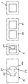
また、フィルム基板の例として、四角形、L型、C型、I型などの種々の形状の場合があり、各形状のフィルム基板においては、スルーホールと接合面を避けた場所を吸着するのが好ましい。例えば、図30(A),(B),(C)に示すように、L型フィルム基板、C型フィルム基板、I型フィルム基板では、それぞれ、スルーホールと接合面を避けて一定距離離れた黒丸の2箇所を吸着するのが好ましい。 In addition, examples of the film substrate include various shapes such as a quadrangle, an L shape, a C shape, and an I shape. In each shape of the film substrate, a place avoiding the through hole and the joint surface is adsorbed. preferable. For example, as shown in FIGS. 30A, 30B, and 30C, the L-type film substrate, the C-type film substrate, and the I-type film substrate are spaced apart from each other by avoiding the through hole and the bonding surface, respectively. It is preferable to adsorb two black circles.
なお、上記様々な実施形態のうちの任意の実施形態を適宜組み合わせることにより、それぞれの有する効果を奏するようにすることができる。 It is to be noted that, by appropriately combining arbitrary embodiments of the various embodiments described above, the effects possessed by them can be produced.
1…基板搬入スライダ、2…フィルム基板、3A,3B…搬送アーム装置、4…移動装置、4a…移動体、4b…ガイド部材、4c…サーボモータ、6…アーム部、6a…アーム部駆動装置、7…吸着部、7a…吸着部昇降装置、8…プラズマ処理チャンバー、8A…第1チャンバー、8B…第2チャンバー、8a…蓋、8b…基板電極、8c…高周波電源、8e…カバー、8g…絶縁材、8h…冷却水流路、8i…冷却水用配管、8k…インシュレータ、8m…チャンバーの側壁、8n…チャンバーのベース、8p…静電吸着用のDC電極、8q…水冷ジャケット、8r…高周波印加電極、8t…基板静電吸着用のDC電源、9…基板搬出スライダ、10…プラズマ処理装置本体、20…コントローラ、40…プラズマ処理装置、41…ローダ、42…ICボンダ、42a…基板保持装置、43…接着剤塗布装置、44…部品実装装置、45…FPCボンダ、46…検査装置、47…アンローダ、60…連通管、SHv…直結弁、A…基板搬入準備位置、B…基板搬入位置、C…基板搬出準備位置、D…基板搬出位置。
DESCRIPTION OF
Claims (2)
上記プラズマ処理装置本体内の基板搬出準備位置と上記プラズマ処理装置本体外の基板搬出位置との間で上記フィルム基板を移動させる基板搬出スライダと、
上記プラズマ処理装置本体内に配置され、上記フィルム基板を静電吸着により吸着保持する基板電極を備え、その内部を排気しつつ反応ガスを導入して減圧下で高周波電力を上記基板電極に印加してプラズマを発生させて上記フィルム基板から有機物を除去するプラズマ処理が上記内部にて行われるチャンバーと、
上記基板搬入位置に移動された上記フィルム基板を吸着保持するノズルを有し、そのノズルにより吸着保持された上記フィルム基板を上記チャンバーの上記基板電極に移動させる、基板搬入用の第1搬送アーム装置と、
上記プラズマ処理された上記フィルム基板を吸着保持するノズルを有し、そのノズルにより吸着保持された上記フィルム基板を上記チャンバーの上記基板電極から上記基板搬送準備位置に移動させる、基板搬出用の第2搬送アーム装置と、
を備えた減圧プラズマ処理装置であって、
上記基板電極への静電チャック電圧の印加を開始し所定の電圧値に安定した後、上記第1搬送アーム装置のノズルによる上記フィルム基板の吸着保持を解除するとともにブローすることにより上記第1搬送アーム装置のノズルから上記基板電極に上記フィルム基板を受け渡すように制御するとともに、
上記基板電極への静電チャック電圧の印加を停止し始めると同時に、上記第2搬送アーム装置のノズルによる上記プラズマ処理されたフィルム基板の吸着保持を開始することにより上記基板電極から上記第2搬送アーム装置のノズルに上記プラズマ処理されたフィルム基板を受け渡すように制御する制御手段
を備えることを特徴とする減圧プラズマ処理装置。 A substrate loading slider for moving the film substrate between a substrate loading preparation position outside the plasma processing apparatus main body and a substrate loading position within the plasma processing apparatus main body;
A substrate unloading slider for moving the film substrate between a substrate unloading preparation position in the plasma processing apparatus main body and a substrate unloading position outside the plasma processing apparatus main body;
A substrate electrode disposed in the plasma processing apparatus main body and holding the film substrate by electrostatic adsorption is introduced. A reactive gas is introduced while exhausting the inside of the film substrate, and high-frequency power is applied to the substrate electrode under reduced pressure. A chamber in which plasma treatment is performed to generate plasma and remove organic substances from the film substrate;
A first transfer arm device for carrying a substrate having a nozzle for sucking and holding the film substrate moved to the substrate carry-in position and moving the film substrate sucked and held by the nozzle to the substrate electrode of the chamber When,
A second substrate for carrying out the substrate having a nozzle for sucking and holding the plasma-treated film substrate and moving the film substrate sucked and held by the nozzle from the substrate electrode of the chamber to the substrate transport preparation position; A transfer arm device;
A low-pressure plasma processing apparatus comprising:
After the application of the electrostatic chuck voltage to the substrate electrode is started and stabilized to a predetermined voltage value, the suction of the film substrate by the nozzle of the first transport arm device is released and the first transport is performed by blowing. While controlling to deliver the film substrate from the nozzle of the arm device to the substrate electrode,
At the same time as the application of the electrostatic chuck voltage to the substrate electrode starts to be stopped, the second transport arm device starts to suck and hold the plasma-treated film substrate by the nozzle of the second transport arm device, thereby starting the second transport from the substrate electrode. A reduced-pressure plasma processing apparatus, comprising: control means for controlling to deliver the plasma-treated film substrate to a nozzle of an arm device.
上記基板搬入位置に位置した上記フィルム基板を、基板搬入用の第1搬送アーム装置に備えられたノズルにより吸着保持した状態でチャンバー内の基板電極に搬入し、
上記チャンバー内を排気しつつ反応ガスを導入して減圧下で高周波電力を静電吸着により上記フィルム基板を吸着保持した上記基板電極に印加してプラズマを発生させて上記フィルム基板から有機物を除去するプラズマ処理を行い、
上記基板電極に静電吸着保持され上記プラズマ処理された上記フィルム基板を、基板搬出用の第2搬送アーム装置に備えられたノズルにより吸着保持して上記チャンバーから取り出して上記プラズマ処理装置本体内の基板搬出準備位置に位置させ、
上記基板搬出準備位置に位置した上記フィルム基板を上記プラズマ処理装置本体外に搬出するようにした減圧プラズマ洗浄方法であって、
上記チャンバー内の上記基板電極に搬入するとき、上記基板電極への静電チャック電圧の印加を開始し所定の電圧値に安定した後、上記第1搬送アーム装置のノズルによる上記フィルム基板の吸着保持を解除するとともにブローすることにより上記第1搬送アーム装置のノズルから上記基板電極に上記フィルム基板を受け渡すとともに、
上記チャンバーから上記プラズマ処理された上記フィルム基板を取り出すとき、上記基板電極への静電チャック電圧の印加を停止し始めると同時に、上記第2搬送アーム装置のノズルによる上記プラズマ処理されたフィルム基板の吸着保持を開始することにより上記基板電極から上記第2搬送アーム装置のノズルに上記プラズマ処理されたフィルム基板を受け渡すようにしたことを特徴とする減圧プラズマ洗浄方法。 The film substrate is carried from the outside of the plasma processing apparatus main body to the substrate carrying position in the plasma processing apparatus main body,
The film substrate located at the substrate carry-in position is carried into the substrate electrode in the chamber in a state of being sucked and held by the nozzle provided in the first carrying arm device for carrying in the substrate,
The reaction gas is introduced while evacuating the chamber, and high-frequency power is applied to the substrate electrode holding the film substrate by electrostatic adsorption under reduced pressure to generate plasma to remove organic substances from the film substrate. Perform plasma treatment,
The film substrate that has been electrostatically adsorbed and held on the substrate electrode and that has been subjected to the plasma treatment is adsorbed and held by a nozzle provided in a second transfer arm device for carrying out the substrate, taken out of the chamber, Position it at the board unloading preparation position,
A reduced-pressure plasma cleaning method in which the film substrate positioned at the substrate unloading preparation position is unloaded from the plasma processing apparatus main body,
When the substrate electrode in the chamber is carried in, the application of the electrostatic chuck voltage to the substrate electrode is started and stabilized at a predetermined voltage value, and then the film substrate is sucked and held by the nozzle of the first transfer arm device. The film substrate is transferred from the nozzle of the first transfer arm device to the substrate electrode by releasing and blowing,
When the plasma-treated film substrate is taken out of the chamber, the application of the electrostatic chuck voltage to the substrate electrode starts to be stopped, and at the same time, the plasma-treated film substrate by the nozzle of the second transfer arm device A vacuum plasma cleaning method, wherein the plasma-treated film substrate is delivered from the substrate electrode to the nozzle of the second transfer arm device by starting suction holding.
Priority Applications (1)
| Application Number | Priority Date | Filing Date | Title |
|---|---|---|---|
| JP2007123072A JP4440284B2 (en) | 2007-05-08 | 2007-05-08 | Low pressure plasma processing apparatus and method |
Applications Claiming Priority (1)
| Application Number | Priority Date | Filing Date | Title |
|---|---|---|---|
| JP2007123072A JP4440284B2 (en) | 2007-05-08 | 2007-05-08 | Low pressure plasma processing apparatus and method |
Related Parent Applications (1)
| Application Number | Title | Priority Date | Filing Date |
|---|---|---|---|
| JP2001320472A Division JP4027072B2 (en) | 2001-10-18 | 2001-10-18 | Low pressure plasma processing apparatus and method |
Publications (2)
| Publication Number | Publication Date |
|---|---|
| JP2007214594A JP2007214594A (en) | 2007-08-23 |
| JP4440284B2 true JP4440284B2 (en) | 2010-03-24 |
Family
ID=38492690
Family Applications (1)
| Application Number | Title | Priority Date | Filing Date |
|---|---|---|---|
| JP2007123072A Expired - Fee Related JP4440284B2 (en) | 2007-05-08 | 2007-05-08 | Low pressure plasma processing apparatus and method |
Country Status (1)
| Country | Link |
|---|---|
| JP (1) | JP4440284B2 (en) |
Families Citing this family (1)
| Publication number | Priority date | Publication date | Assignee | Title |
|---|---|---|---|---|
| JP5382444B2 (en) * | 2009-11-09 | 2014-01-08 | 株式会社エスイー | Method and apparatus for forming conductive pattern |
Family Cites Families (3)
| Publication number | Priority date | Publication date | Assignee | Title |
|---|---|---|---|---|
| JPH0590796A (en) * | 1991-09-26 | 1993-04-09 | Japan Tobacco Inc | Work mounting apparatus |
| JPH07147311A (en) * | 1993-11-24 | 1995-06-06 | Tokyo Electron Ltd | Transfer arm |
| JP2000124679A (en) * | 1998-10-13 | 2000-04-28 | Sanyo Electric Co Ltd | Automatic electronic component-mounting device |
-
2007
- 2007-05-08 JP JP2007123072A patent/JP4440284B2/en not_active Expired - Fee Related
Also Published As
| Publication number | Publication date |
|---|---|
| JP2007214594A (en) | 2007-08-23 |
Similar Documents
| Publication | Publication Date | Title |
|---|---|---|
| JP4027072B2 (en) | Low pressure plasma processing apparatus and method | |
| KR102459565B1 (en) | Pick, transfer device and plasma processing system | |
| JP4697066B2 (en) | Electrode bonding method and component mounting apparatus | |
| KR102290822B1 (en) | Bonding system and bonding method | |
| WO2012121046A1 (en) | Bonding device, bonding system and bonding method | |
| JP2006181641A (en) | Bonding apparatus and bonding method | |
| JP4377035B2 (en) | Mounting method and apparatus | |
| CN100450329C (en) | Film substrate processing device and film substrate processing method | |
| JP4440284B2 (en) | Low pressure plasma processing apparatus and method | |
| JP4344320B2 (en) | Joining device | |
| JP6855334B2 (en) | Substrate processing equipment and substrate processing method | |
| JP4186495B2 (en) | Electronic component mounting device | |
| WO2022181655A1 (en) | Bonding method, substrate bonding device, and substrate bonding system | |
| KR102299883B1 (en) | Apparatus and Method for treating substrate | |
| JP3462850B2 (en) | Semiconductor component manufacturing method and plasma cleaning apparatus | |
| JP2004119664A (en) | Method and device for joining | |
| JP6174210B2 (en) | Mounting table and plasma processing apparatus | |
| CN118692930A (en) | Method of forming a joint assembly and apparatus for forming a joint assembly | |
| JP2008177512A (en) | Apparatus for removing unnecessary object from peripheral edge of substrate, semiconductor manufacturing apparatus and method for removing unnecessary object from peripheral edge of substrate | |
| JP2023138347A (en) | Mounting device and mounting method | |
| CN118782477A (en) | Joining method and joining system | |
| JP2000173967A (en) | Substrate transfer mechanism of plasma cleaning equipment | |
| WO2024147351A1 (en) | Bonding method, bonding system, illumination device, and activation processing device | |
| CN115910893A (en) | Joining device and joining method | |
| CN118692883A (en) | Method of forming a joint assembly and apparatus for forming a joint assembly |
Legal Events
| Date | Code | Title | Description |
|---|---|---|---|
| A131 | Notification of reasons for refusal |
Free format text: JAPANESE INTERMEDIATE CODE: A131 Effective date: 20090602 |
|
| A521 | Written amendment |
Free format text: JAPANESE INTERMEDIATE CODE: A523 Effective date: 20090706 |
|
| A131 | Notification of reasons for refusal |
Free format text: JAPANESE INTERMEDIATE CODE: A131 Effective date: 20090929 |
|
| A521 | Written amendment |
Free format text: JAPANESE INTERMEDIATE CODE: A523 Effective date: 20091014 |
|
| TRDD | Decision of grant or rejection written | ||
| A01 | Written decision to grant a patent or to grant a registration (utility model) |
Free format text: JAPANESE INTERMEDIATE CODE: A01 Effective date: 20091208 |
|
| A01 | Written decision to grant a patent or to grant a registration (utility model) |
Free format text: JAPANESE INTERMEDIATE CODE: A01 |
|
| A61 | First payment of annual fees (during grant procedure) |
Free format text: JAPANESE INTERMEDIATE CODE: A61 Effective date: 20100106 |
|
| FPAY | Renewal fee payment (event date is renewal date of database) |
Free format text: PAYMENT UNTIL: 20130115 Year of fee payment: 3 |
|
| R150 | Certificate of patent or registration of utility model |
Free format text: JAPANESE INTERMEDIATE CODE: R150 |
|
| FPAY | Renewal fee payment (event date is renewal date of database) |
Free format text: PAYMENT UNTIL: 20130115 Year of fee payment: 3 |
|
| LAPS | Cancellation because of no payment of annual fees |