JP4404460B2 - Multi-cavity wiring board, wiring board, multi-cavity semiconductor element storage package and semiconductor element storage package - Google Patents
Multi-cavity wiring board, wiring board, multi-cavity semiconductor element storage package and semiconductor element storage package Download PDFInfo
- Publication number
- JP4404460B2 JP4404460B2 JP2000240986A JP2000240986A JP4404460B2 JP 4404460 B2 JP4404460 B2 JP 4404460B2 JP 2000240986 A JP2000240986 A JP 2000240986A JP 2000240986 A JP2000240986 A JP 2000240986A JP 4404460 B2 JP4404460 B2 JP 4404460B2
- Authority
- JP
- Japan
- Prior art keywords
- wiring
- wiring pattern
- wiring board
- pattern
- semiconductor element
- Prior art date
- Legal status (The legal status is an assumption and is not a legal conclusion. Google has not performed a legal analysis and makes no representation as to the accuracy of the status listed.)
- Expired - Fee Related
Links
Images


Landscapes
- Structure Of Printed Boards (AREA)
Description
【0001】
【発明の属する技術分野】
本発明は、一つの基板から多数個の配線基板を分割して作製するための多数個取り配線基板、その多数個取り配線基板から作製される配線基板、多数個取り配線基板を用いた多数個取り半導体素子収納用パッケージ、および配線基板を用いた半導体素子収納用パッケージに関するものである。
【0002】
【従来の技術】
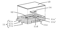
従来の、高周波信号で作動する半導体素子を収納する半導体素子収納用パッケージ(以下、半導体パッケージという)のうち、リードレスチップキャリアパッケージ(LCCパッケージ)の斜視図を図6に示す。同図に示すように、このLCCパッケージは、一般に上面に半導体素子14が載置される載置部11dを有するアルミナ(Al2O3)セラミックス,窒化アルミニウム(AlN)セラミックス等のセラミック基板を複数枚積層した基体11から成る。
【0003】
この基体11の第1のセラミック基板11a,第2のセラミック基板11bの側面に溝を設けるとともに、その溝の内面に電解メッキ層等から成る導電部を設ける。そして、外部の実装基板(図示せず)と、半導体パッケージ内部に形成されシグナル(S)ラインとグランド(G)ラインが交互に形成された配線パターン12とが、電極パッド(外部接続端子)11eにより、電気的に接続される。この電極パッド11eは上記の溝の内面に形成された導電部から成る。
【0004】
また、基体11の第3のセラミック基板11cの側面には、蓋体13との接合面積を大きくして蓋体13の基体11に対する接合を強固なものとするために、第1のセラミック基板11a,第2のセラミック基板11bのような溝は形成されておらず、この第3のセラミック基板11cは所謂シールリングとしての機能を有する。
【0005】
このような半導体パッケージは、非常に小型であるため母基板となる1枚のセラミックグリーンシートに分割線(スリット)を設け、複数枚積層し焼結してセラミックスとした後に電解メッキを施し、その後分割線で分割することにより個々の製品(LCCパッケージ)とするといった所謂多数個取りにより製造するのがよい。この多数個取りにより製造した方が、分割された個々のセラミックグリーンシートを積層し焼結するよりも製造を非常に容易にでき、またコストを低く抑えることができる。
【0006】
そのため、基体11は、図7〜図9のそれぞれの平面図に示す、第1のセラミック基板11a,第2のセラミック基板11b,第3のセラミック基板11c用のセラミックグリーンシートを積層し、焼結してセラミックスとした後に電解メッキを施し、その後分割線で分割することにより半導体パッケージ用の基体11として作製される。
【0007】
第1のセラミック基板11aとなるセラミックグリーンシート上には、図7に平面図を示すように、半導体素子14の載置部11dが設けられるとともに貫通孔11e’が設けられ、この貫通孔11e’の略中央部を横断するように跨って分割線が設けられている。
【0008】
また、第2のセラミック基板11bとなるセラミックグリーンシートには、図8の平面図,図10の拡大平面図に示すように、分割線と中央部の貫通孔(開口)11b’とが形成されるとともに、略中央部が分割線を跨るようにして形成され、個々の配線基板に分割された際に電極パッド11eを構成する貫通孔11e’が設けられる。さらに、この貫通孔11e’の分割線に対して両側に接続されるように配線パターン12が形成される。また、これら貫通孔11e’の内周面と配線パターン12とに電解メッキを施すために、貫通孔11e’間で分割線を横切るように葛折状に導通パターン15が形成されている。
【0009】
また、第3のセラミック基板11cとなるセラミックグリーンシートには、図9に平面図を示すように、図8,図10の中央部の貫通孔11b’よりも若干大きく設けられた貫通孔11c’が、分割線とともに形成されている。
【0010】
なお、第1のセラミック基板11aの貫通孔11e’内周面における電解メッキは、第1のセラミック基板11aと第2のセラミック基板11bとを積層した際に、それぞれの貫通孔11e’が接触し導通することにより行われる。
【0011】
このように、電解メッキ用の導通パターン15は、電解メッキする際に全ての貫通孔11e’および配線パターン12を電気的に接続することができ、さらには、個々の製品(半導体パッケージ)に分割線で分割した際に分割面で導通パターン15が切断されるため、各々の配線パターンを電気的に短絡させることはない。
【0012】
このような基体11は、その載置部11dに半導体素子14が金(Au)−ゲルマニウム(Ge)等の低融点ロウ材や樹脂接着剤で接合されるとともに、配線パターン12に半導体素子14の電極がボンディングワイヤ(図示せず)を介して電気的に接続される。さらに、基体11の上面に、鉄(Fe)−ニッケル(Ni)−コバルト(Co)合金,鉄(Fe)−ニッケル(Ni)合金等の金属材料や、アルミナセラミックス,窒化アルミニウムセラミックス等のセラミックスから成る蓋体13が、シーム溶接等による溶接や、金(Au)−錫(Sn)半田等の低融点ロウ材による接着により接合される。このようにして半導体素子14を内部に収納した製品としての半導体装置となる。
【0013】
このような半導体装置は、その電極パッド11eを介して外部の実装基板に錫(Sn)−鉛(Pb)半田等の低融点半田で電気的に接続され、実装基板との高周波信号の授受により半導体素子14を作動させる。
【0014】
【発明が解決しようとする課題】
しかしながら、上記従来の半導体パッケージにおいて、例えば10GHz以上の高周波信号の場合に作動するような半導体素子14を半導体パッケージ内部に収納し半導体装置と成した後、外部の実装基板に接続し半導体素子14を作動させた場合、分割線で分割した際の貫通孔11e’の周辺部に残存している導通パターン15の切れ端により、高周波信号が配線パターン12のシグナルラインのみならず導通パターン15の切れ端にも迂回するように伝送される。そのため、高周波信号の伝送損失が大きくなり、高周波信号の伝達が円滑になされないという問題点を有していた。
【0015】
従って、本発明は上記問題点に鑑み完成されたもので、その目的は、配線パターンのシグナルラインを伝送する高周波信号の伝送特性を円滑なものとすることにより、半導体素子の高周波信号による作動性を良好なものとすることにある。
【0016】
【課題を解決するための手段】
本発明の多数個取り配線基板は、セラミックスから成る母基板の主面に分割線で区切られた略四角形の複数の配線基板領域が縦横に配列形成された多数個取り配線基板において、隣接する配線基板領域の間で前記分割線を横切って形成された複数の配線パターンと、隣接する配線パターン間で前記分割線を越えて形成され、かつ1本の前記配線パターンに対して一方のみの前記配線基板領域において接続されている導通パターンとを具備し、前記配線パターンは、前記分割線の両側に信号用の前記配線パターンと接地用の前記配線パターンとが設けられ、各前記配線基板領域において、前記信号用の前記配線パターンと前記接地用の前記配線パターンとが交互に配置されており、前記接地用の前記配線パターンのみが前記導通パターンと接続していることを特徴とする。
【0017】
本発明は、上記の構成により、分割線に沿って分割して配線基板を作製した際に、導通パターンは例えば一つおきの配線パターンに接続された状態で配線基板の周辺部に残存することになり、その導通パターンが接続した配線パターンを信号用としてではなく接地用として用いることにより、信号用の配線パターンを伝搬する高周波信号の伝送損失を小さくすることができる。
【0018】
また、本発明の配線基板は、外形が略四角形のセラミック基板の主面に、周辺部と中央部の間に形成されたn本(nは2以上の整数)の配線パターンと、前記配線パターンのうち1〜m本{ただし、nが偶数の場合m=n/2、nが奇数の場合m=(n+1)/2である}に設けられるとともに、前記配線パターンの途中から両側に前記周辺部に向かって枝分かれするように付加された導通パターンとを具備し、隣接する前記配線パターンは、前記導通パターンが周囲に残存しない信号用の前記配線パターンと前記導通パターンが接続された状態で残存した接地用の前記配線パターンとが交互に形成されており、前記信号用の前記配線パターンのみが高周波信号を伝送することを特徴とする。
【0019】
本発明は、上記の構成により、多数個取り配線基板を分割線で分割した後に、隣接する配線パターンにおいて、導通パターンが周囲に残存しない配線パターンと導通パターンが接続された状態で残存した配線パターンとが、交互に形成されることとなる。この導通パターンが周囲に残存しない配線パターンをシグナルラインとすると、高周波信号はシグナルライン用の配線パターンのみを伝送し、従来のように導通パターンの切れ端に迂回するといったことがなくなる。従って、電解メッキ用の導通パターンを本発明のごとくすることで、高周波信号の伝送特性に優れた信頼性の高い製品を提供することができる。
【0020】
また、本発明の多数個取り半導体素子収納用パッケージは、上面に半導体素子を載置する載置部を有する、分割線で区切られた搭載用基板領域が複数形成された多数個取り配線基板と、各前記半導体素子を封止する複数の蓋体とを具備する多数個取り半導体素子収納用パッケージにおいて、前記多数個取り配線基板が請求項1記載の多数個取り配線基板であることを特徴とする。
【0021】
本発明は、上記の構成により、多数個取り配線基板を分割線で分割した後に、配線基板において、隣接する配線パターンにおいて、導通パターンが周囲に残存しない配線パターンと導通パターンが接続された状態で残存した配線パターンとが、交互に形成されることとなる。この導通パターンが周囲に残存しない配線パターンをシグナルラインとすると、高周波信号はシグナルライン用の配線パターンのみを伝送し、従来のように導通パターンの切れ端に迂回するといったことがなくなる。その結果、半導体素子の高周波信号による作動性を非常に良好なものとした半導体パッケージを提供することができる。
【0022】
また、本発明の半導体素子収納用パッケージは、上面に半導体素子を載置する載置部を有する搭載用基板と、前記半導体素子を封止する蓋体とを具備した半導体素子収納用パッケージにおいて、前記搭載用基板が上記本発明の配線基板であることを特徴とする。
【0023】
本発明は、上記の構成により、多数個取り配線基板を分割線で分割した後に、配線基板において、隣接する配線パターンにおいて、導通パターンが周囲に残存しない配線パターンと導通パターンが接続された状態で残存した配線パターンとが交互に形成されることとなる。この導通パターンが周囲に残存しない配線パターンをシグナルラインとすると、高周波信号はシグナルライン用の配線パターンのみを伝送し、従来のように導通パターンの切れ端に迂回するといったことがなくなる。その結果、半導体素子の高周波信号による作動性を非常に良好なものとした半導体パッケージを提供することができる。
【0024】
【発明の実施の形態】
本発明の半導体パッケージを以下に詳細に説明する。図1は本発明の半導体パッケージの一実施形態を示す斜視図、図2〜図4は積層前の各セラミックグリーンシートを示す平面図、図5は導通パターンの形成の一例を示す拡大平面図である。これらの図において、1は基体、3は蓋体、4は半導体素子である。これら基体1と蓋体3とで、内部に半導体素子4を収納するための容器が構成される。
【0025】
基体1は、その上面に凹部を有するとともに、その外側側面に、内周面に電解メッキが施され電極パッド1eとなる溝が設けられ、アルミナセラミックス,窒化アルミニウムセラミックス等の各種セラミックスから成る。また、基体1の凹部の底面に半導体素子4を載置固定する載置部1dを有している。このような基体1は、半導体素子4の載置固定部材として機能し、また基体1用のセラミックスの材質は半導体素子4の電気特性に応じて適宜選定される。
【0026】
また、この基体1は、例えばアルミナセラミックスから成る場合、以下のようにして作製される。まず、酸化アルミニウム(Al2O3),酸化珪素(SiO2),酸化マグネシウム(MgO),酸化カルシウム(CaO)等の原料粉末に有機バインダ、溶剤等を添加混合してペーストを作製する。そのペーストをドクターブレード法やカレンダーロール法等を採用することによって、1枚または複数枚から成る、第1のセラミック基板1a,第2のセラミック基板1b,第3のセラミック基板1cとなるセラミックグリーンシートを作製する。これらのセラミックグリーンシートに、必要に応じて貫通孔1e’、および各配線基板領域の中央部に設けられる半導体素子4挿置用の貫通孔1b’,1c’を形成するための打ち抜き加工を施し、しかる後配線パターン2や導通パターン5となる部位や貫通孔1e’内周面に、モリブデン(Mo)−マンガン(Mn)やタングステン(W)等の金属ペーストを印刷塗布する。そして、これらを積層し約1600℃の温度で焼結しセラミックスとした後、第1,第2,第3のセラミック基板1a,1b,1cが、上下で対応して重なるように形成された分割線で分割されることにより、個々の半導体パッケージとして作製される。
【0027】
なお、各セラミックグリーンシートにおいて、貫通孔1e’を形成しなくてもよく、その場合、半導体パッケージと成した際には、積層された第1,第2,第3のセラミック基板1a,1b,1cの側面に配線パターン2に接続されたメタライズ配線層等から成る電極パッド1eを形成してもよい。
【0028】
このような基体1の第1のセラミック基板1aとなる第1のセラミックグリーンシートの一方の主面には、図2の平面図に示すように、分割線で区切られた長方形等の略四角形の基板領域が縦横に配列形成される。この基板領域内に半導体素子4の載置部1dが設けられる。また、この分割線の線上に貫通孔1e’が設けられる。即ち、この貫通孔1e’の略中央部を横断するように跨って分割線が設けられる。この貫通孔1e’は、同じ構成の基板を多数形成するために、各基板領域同士で分割線上の同様の箇所に形成される。
【0029】
基体1の第2のセラミック基板1bとなる第2のセラミックグリーンシートの一方の主面には、図3の平面図,図5の拡大平面図に示すように、第1のセラミックグリーンシート上の分割線に対応する分割線で区切られた、半導体素子4を取り囲むための貫通孔1b’が中央に形成された、外形が四角形で枠状の配線基板領域が縦横に配列形成される。各配線基板領域では、分割線上に第1のセラミックグリーンシートの貫通孔1e’に対応する貫通孔1e’が形成される。即ち、第2のセラミックグリーンシートの貫通孔1e’の略中央部を横断するように跨って第2のセラミックグリーンシート上に分割線が設けられる。
【0030】
第2のセラミックグリーンシートの貫通孔1e’から貫通孔1b’側に延びる配線パターン2を形成するに際し、各配線基板領域において、信号{シグナル(S)}用の配線パターン2と接地{グランド(G)}用の配線パターン2とが、交互に配置されるように形成する。この場合、貫通孔1e’がなければ、配線パターン2は互いに隣接する配線基板領域同士の間で分割線を横切って形成される。
【0031】
また、隣接する配線基板領域間で、貫通孔1e’に対して分割線の両側に、信号用の配線パターン2と接地用の配線パターン2とが設けられる。即ち、一つの貫通孔1e’に対して、一方に信号用の配線パターン2が他方に接地用の配線パターン2が配置されるように形成される。
【0032】
さらには、貫通孔1e’内周面と配線パターン2とに電解メッキを施すために、貫通孔1e’間で分割線を越えて、葛折状等のパターンで導通パターン5が形成されている。この場合、貫通孔1e’がなければ、導通パターン5は、分割線に近接してその方向に合うように、または沿うように形成されるとともに、隣接する配線パターン2間で分割線を越えて形成され、かつ1本の配線パターン2において分割線に対して一方のみの配線基板領域において配線パターンに接続されている。
【0033】
導通パターン5が隣接する配線パターン2間で分割線を越える回数は、図3,図5に示すように1回でよいが、複数回とする場合3回以上の奇数回とれば、導通パターン5は隣接する配線パターン2において分割線に対して反対側の配線基板領域へ移ることとなる。また、導通パターン5が隣接する配線パターン2間で分割線を越える回数を偶数回とすれば、導通パターン5は隣接する配線パターン2において分割線に対して反対側の配線基板領域へ移ることはない。このように、分割線を越える回数を調整することで、一つの配線基板領域で配線パターン2に接続される導通パターン5の接続箇所数を調整できる。また、導通パターン5が隣接する配線パターン2間で分割線を越える回数を1回とすれば、一つの配線基板領域で配線パターン2に導通パターン5は交互に接続されることとなる。
【0034】
また、導通パターン5は分割線を横断するように形成される構成に限らず、分割線を斜めに越えるように形成してもよい。
【0035】
この導通パターン5は、貫通孔1e’が線上に存在する分割線に近接してその方向に合うように形成されるとともに、分割線に対して貫通孔1e’の接地用の配線パターン2側の開口縁に常に接するように、貫通孔1e’間で分割線を横断等して越えて、葛折状等に形成される。その結果、導通パターン5は、分割線で分割した際に、貫通孔1e’の信号用の配線パターン2側の周辺部に切れ端が残存しないものとなる。換言すると、分割線に対して貫通孔1e’の接地用の配線パターン2側に設けられている。
【0036】
これにより、導通パターン5の貫通孔1e’への接合は、各配線基板領域を分割線で分割した後に、高周波信号が伝送されるシグナルラインの周辺部に導通パターン5の切れ端が残存しないように成される。その結果、高周波信号は、導通パターン5の切れ端に迂回し伝送されることなくシグナルラインのみを伝送するため、高周波信号の伝送が円滑なものと成る。従って、半導体素子4の高周波信号による作動性を非常に良好なものとできる。
【0037】
また、この導通パターン5は、インピーダンス特性を良好なものとするために、例えば信号用と接地用とが交互に配置形成されるように貫通孔1e’に接続される。なお、グランドラインは、導通ライン5の切れ端が貫通孔1e’の周辺部に残存しても高周波伝送特性が損なわれることはない。
【0038】
なお、シグナルラインは、配線パターン2とそれに接続された貫通孔1e’の導体とで構成される高周波信号の伝送路であり、グランドラインは、配線パターン2とそれに接続された貫通孔1e’の導体とで構成される接地電位の導電路である。
【0039】
このような配線パターン2自体の構成は、信号用と接地用とで特に区別されるものではないが、シグナルラインの左右隣にグランドラインを形成しておくほうが、インピーダンス特性を良好なものとできる。
【0040】
また、配線基板としての分割された個々の第2のセラミック基板1bは、以下のような構成となる。即ち、外形が略四角形の枠状の第2のセラミック基板1bの主面に、周辺部と中央部(貫通孔1b’)の間に形成されたn本(nは2以上の整数)の配線パターン2と、配線パターンのうち1〜m本{ただし、nが偶数の場合m=n/2、nが奇数の場合m=(n+1)/2である}に設けられるとともに、配線パターン2の途中から両側に周辺部に向かって枝分かれするように付加された導通パターン5とを具備し、隣接する配線パターン2は、導通パターン5が周囲に残存しない信号用の配線パターン2と導通パターン5が接続された状態で残存した接地用の配線パターン2とが交互に形成されており、信号用の配線パターン2のみが高周波信号を伝送する構成である。この場合、配線基板の主面の中央部に形成された貫通孔1b’については、配線基板を単一で使用する場合等には特に必要なものではないが、図1のような積層型配線基板の中間の1層として使用する場合等には貫通孔1b’を設けることとなる。
【0041】
第3のセラミック基板1cとなる第3のセラミックグリーンシートの主面には、図4に示すように、第2のセラミックグリーンシート上の分割線に対応する分割線で区切られた、中央部に貫通孔1c’が形成された外形が四角形で枠状の基板領域が縦横に配列形成されている。また、図4の平面図に示すように、図3,図5の貫通孔1b’よりも開口幅が若干大きく形成された貫通孔1c’が形成される。これは、図1に示すように、基体1の凹部を下方に向かって段階的に狭くする構成とするためである。
【0042】
この第3のセラミック基板1cは、その上面が、半導体素子4を封止するための蓋体3がシーム溶接等による溶接や金(Au)−錫(Sn)半田等の低融点ロウ材による接着により強固に接合されるシール部材、所謂シールリングとして機能する。また、その枠の幅は接合強度を維持するような適度な大きさとされる。
【0043】
なお、第1のセラミック基板1aの貫通孔1e’内周面における電解メッキは、第1のセラミック基板1aと第2のセラミック基板1bとを積層した際に、それぞれの貫通孔1e’が接触し導通することにより行われる。
【0044】
このように導通パターン5は、積層し焼結した後にニッケル(Ni)メッキ,金(Au)メッキ等の耐食性に優れた電解メッキを施す際に、全ての貫通孔1e’および配線パターン2を電気的に接続するものである。また、個々の製品(半導体パッケージ)に分割した際に、分割面で導通パターン5が切断されるため、各々の配線パターン2を電気的に短絡させず、さらには高周波信号が伝送されるシグナルラインの周辺部に導通パターン5の切れ端が残存しない。
【0045】
かくして、本発明の半導体パッケージは、基体1の略中央部に設けられる貫通孔1b’,1c’と、基体1の外側側面に設けられ、貫通孔1e’を縦方向に分割して形成された溝から成り外部との電気的接続を行う電極パッド1eとなる溝と、第1,第2,第3の各セラミックグリーンシートに設けられた貫通孔1e’の上端開口の略中央部を横断する分割線と、第2のセラミックグリーンシートに設けられた貫通孔1e’の分割線に対して両側に接合され、半導体素子4との電気的接続を行うとともに、シグナルラインとグランドラインとが交互に形成される配線パターン2とを有する。
【0046】
また、第2のセラミックグリーンシートに設けられた貫通孔1e’の分割線に対して、シグナルライン側ではなくグランドライン側に設けられており、配線パターン2と第1,第2のセラミックグリーンシートの貫通孔1e’内周面とに電解メッキを施すための導通パターン5を有する。
【0047】
そして、本発明の半導体パッケージは、上面に半導体素子4を載置する載置部1dを有する搭載用基板としての基体1と、半導体素子4を封止する蓋体3とを具備した構成である。
【0048】
図1の場合、半導体パッケージは、貫通孔1b’,1c’と、貫通孔1e’と、分割線と、配線パターン2と、導通パターン5とが設けられた、第1〜第3のセラミックグリーンシートを積層し焼結し電解メッキを施した後、第1,第2,第3の各セラミックグリーンシートを上下方向で重なるように対応する分割線で分割することにより作製される。その結果、この半導体パッケージの上面には凹部が形成され、この凹部底面に半導体素子4を載置する載置部1dを有する基体1を有するものとなる。
【0049】
即ち、上面に半導体素子4を載置する載置部1dを有する第1のセラミック基板1aと、第1のセラミック基板1a上面に積層され、半導体素子4と外部との電気的接続を行う枠状の第2のセラミック基板1bと、第2のセラミック基板1b上面に積層され、上面に半導体素子4を封止する蓋体3を接合するための枠状の第3のセラミック基板1cとから成る基体1を具備した半導体パッケージと成る。
【0050】
また、本発明の半導体パッケージは、図1のような基体1の上面に凹部を形成したものに限らず、平板状の基体の上面の周縁部にキャップ状の蓋体を接合させたものであってもよい。
【0051】
これにより、多数個取り用の母基板である焼結後のセラミック多層基板を分割線で分割しても、個々の第2のセラミック基板1bにおいて配線パターン2のシグナルラインとなる部位には導通パターン5の切れ端が残存することがない。そのため、高周波信号はシグナルラインのみを伝送することとなり、半導体素子4の作動性が非常に良好なものとなる。
【0052】
このように、セラミックグリーンシートを複数枚積層し、焼結し電解メッキが施されて成る各セラミック基板1a,1b,1cを分割線で分割し基体1と成した後、載置部1dに半導体素子4を金(Au)−ゲルマニウム(Ge)等の低融点ロウ材や樹脂接着剤を介して載置固定し、半導体素子4の電極を配線パターン2にボンディングワイヤを介して電気的に接続する。その後、基体1の上面に鉄(Fe)−ニッケル(Ni)−コバルト(Co)合金,鉄−ニッケル合金等の金属材料や、アルミナセラミックス,窒化アルミニウムセラミックス等のセラミックスから成る蓋体3が、シーム溶接等による溶接や金(Au)−錫(Sn)半田等の低融点ロウ材による接着により接合され、半導体素子4を内部に収納した製品としての半導体装置となる。
【0053】
このような半導体装置は、その電極パッド1eを介して外部の実装基板に錫(Sn)−鉛(Pb)半田等の低融点半田で電気的に接続され、実装基板との高周波信号の授受により半導体素子4を作動させる。
【0054】
さらに、本発明においては、上記本発明の多数個取り配線基板を用いて多数個取り半導体素子収納用パッケージを構成する。その場合、上面に半導体素子4を載置する載置部1dを有する、分割線で区切られた基体1と成る搭載用基板領域が複数形成された多数個取り配線基板と、各半導体素子4を封止する複数の蓋体3とを具備するものである。
【0055】
なお、本発明は上記実施形態に限定されず、本発明の要旨を逸脱しない範囲内において種々の変更を行うことは何等支障ない。
【0056】
例えば、高周波信号で作動する発光素子の1種である半導体レーザ(LD)等の光素子を収納する光半導体素子収納用パッケージの場合においても、本発明を適用できる。また、上記実施形態では、上面に凹部を有し基体1の内層部(第2のセラミック基板1b)に本発明の導通パターン5を有する半導体パッケージの構成について説明したが、本発明の配線基板は、導通パターン5等の配線構造を表層に有する単板の配線基板の場合であってもよいことはいうまでもない。さらには、シグナルラインとグランドラインは、必ずしも交互に配置される必要はなく、即ち、10GHz以上の高周波信号のみでなく、伝送特性を損なわない程度の低い周波数帯域の信号を伝送させる場合は、導通パターン5の切れ端が残存する配線パターン2をシグナルラインとして使用してもよい。上記の実施形態では、第2のセラミックグリーンシートを1層積層させたが、2層以上積層させてもよい。
【0057】
【発明の効果】
本発明の多数個取り配線基板は、隣接する配線基板領域の間で分割線を横切って形成された複数の配線パターンと、隣接する配線パターン間で分割線を越えて形成され、かつ1本の配線パターンに対して一方のみの配線基板領域において接続されている導通パターンとを具備し、配線パターンは、分割線の両側に信号用の配線パターンと接地用の配線パターンとが設けられ、各配線基板領域において、信号用の前記配線パターンと接地用の配線パターンとが交互に配置されており、接地用の配線パターンのみが導通パターンと接続していることにより、配線基板領域を分割線で分割した後に、導通パターンは隣接する配線パターンにおいて一方の配線パターンにのみ接続した状態で配線基板の周辺部に沿うようにして残存することになり、その導通パターンが接続した配線パターンを信号用としてではなく接地用として用いることにより、信号用の配線パターンを伝搬する高周波信号の伝送損失を小さくすることができる。即ち、この導通パターンの切れ端が残存しない部位の配線パターンをシグナルラインとすると、高周波信号はシグナルライン用の配線パターンのみを伝送し、従来のように導通パターンの切れ端に迂回するといったことがなくなる。従って、電解メッキ用の導通パターンを本発明のごとくすることで、高周波信号の伝送特性に優れた信頼性の高い製品を提供することができる。
【0058】
また、本発明の配線基板は、外形が略四角形のセラミック基板の主面に、周辺部と中央部の間に形成されたn本(nは2以上の整数)の配線パターンと、配線パターンのうち1〜m本{ただし、nが偶数の場合m=n/2、nが奇数の場合m=(n+1)/2である}に設けられるとともに、配線パターンの途中から両側に周辺部に向かって枝分かれするように付加された導通パターンとを具備し、隣接する配線パターンは、導通パターンが周囲に残存しない信号用の配線パターンと導通パターンが接続された状態で残存した接地用の配線パターンとが交互に形成されており、信号用の配線パターンのみが高周波信号を伝送することにより、多数個取り配線基板を分割線で分割した後に、隣接する配線パターンにおいて、導通パターンが周囲に残存しない配線パターンと導通パターンが接続された状態で残存した配線パターンとが形成されることとなる。この導通パターンが周囲に残存しない配線パターンをシグナルラインとすると、高周波信号はシグナルライン用の配線パターンのみを伝送し、従来のように導通パターンの切れ端に迂回するといったことがなくなる。従って、電解メッキ用の導通パターンを本発明のごとくすることで、高周波信号の伝送特性に優れた信頼性の高い製品を提供することができる。
【0059】
また、配線パターンに付加された導通パターンは、その配線パターンがグランドラインとして使用される場合接地電位を強化するという効果も有する。
【0060】
本発明の多数個取り半導体素子収納用パッケージは、上面に半導体素子を載置する載置部を有する、分割線で区切られた搭載用基板領域が複数形成された多数個取り配線基板と、各半導体素子を封止する複数の蓋体とを具備する多数個取り半導体素子収納用パッケージにおいて、この多数個取り配線基板が上記本発明の多数個取り配線基板であることにより、上記本発明の多数個取り配線基板の場合と同様の効果を有し、従って半導体素子の高周波信号による作動性を非常に良好とした多数個取り半導体パッケージを提供することができる。
【0061】
本発明の半導体パッケージは、上面に半導体素子を載置する載置部を有する搭載用基板と、半導体素子を封止する蓋体とを具備した半導体素子収納用パッケージにおいて、搭載用基板が上記本発明の配線基板であることにより、上記本発明の配線基板と同様の効果を有し、従って半導体素子の高周波信号による作動性を非常に良好とした半導体パッケージを提供することができる。
【図面の簡単な説明】
【図1】本発明の半導体パッケージの一実施形態を示す分解斜視図である。
【図2】本発明の第1のセラミック基板となる第1のセラミックグリーンシートを示す部分拡大平面図である。
【図3】本発明の第2のセラミック基板となる第2のセラミックグリーンシートを示す部分拡大平面図である。
【図4】本発明の第3のセラミック基板となる第3のセラミックグリーンシートを示す部分拡大平面図である。
【図5】本発明の導通パターンの一例を示す第2のセラミックグリーンシートの部分拡大平面図である。
【図6】従来の半導体パッケージを示す分解斜視図である。
【図7】従来の第1のセラミック基板となるセラミックグリーンシートを示す部分拡大平面図である。
【図8】従来の第2のセラミック基板となるセラミックグリーンシートを示す部分拡大平面図である。
【図9】従来の第3のセラミック基板となるセラミックグリーンシートを示す部分拡大平面図である。
【図10】図8の導通パターンを示すセラミックグリーンシートの部分拡大平面図である。
【符号の説明】
1:基体
1a:第1のセラミック基板
1b:第2のセラミック基板
1c:第3のセラミック基板
1d:載置部
1e’:貫通孔
2:配線パターン
3:蓋体
4:半導体素子
5:導通パターン[0001]
BACKGROUND OF THE INVENTION
The present invention relates to a multi-piece wiring board for dividing and manufacturing a large number of wiring boards from a single board, a wiring board made from the multi-piece wiring board, and a large number using a multi-piece wiring board. The present invention relates to a package for storing semiconductor devices and a package for storing semiconductor devices using a wiring board.
[0002]
[Prior art]
FIG. 6 shows a perspective view of a leadless chip carrier package (LCC package) among conventional semiconductor element storage packages (hereinafter referred to as semiconductor packages) for storing semiconductor elements that operate with high-frequency signals. As shown in the figure, this LCC package generally has alumina (Al) having a
[0003]
A groove is provided on the side surfaces of the first ceramic substrate 11a and the second
[0004]
Further, on the side surface of the third
[0005]
Since such a semiconductor package is very small, a dividing line (slit) is provided on one ceramic green sheet as a mother substrate, and a plurality of layers are laminated and sintered to be ceramics, and then subjected to electrolytic plating. It is preferable to manufacture by so-called multi-cavity such that each product (LCC package) is divided by dividing lines. Manufacture by this multi-cavity can be much easier to manufacture than the individual ceramic green sheets that are divided and laminated and the cost can be kept low.
[0006]
Therefore, the
[0007]
On the ceramic green sheet to be the first ceramic substrate 11a, as shown in a plan view in FIG. 7, a
[0008]
Further, as shown in the plan view of FIG. 8 and the enlarged plan view of FIG. 10, a dividing line and a central through-hole (opening) 11 b ′ are formed on the ceramic green sheet to be the second
[0009]
Further, as shown in a plan view of FIG. 9, the ceramic green sheet to be the third
[0010]
The electrolytic plating on the inner peripheral surface of the through-hole 11e ′ of the first ceramic substrate 11a is such that when the first ceramic substrate 11a and the second
[0011]
Thus, the electroplating
[0012]
In such a
[0013]
Such a semiconductor device is electrically connected to an external mounting substrate via its electrode pad 11e with a low melting point solder such as tin (Sn) -lead (Pb) solder, and exchanges high frequency signals with the mounting substrate. The
[0014]
[Problems to be solved by the invention]
However, in the above-described conventional semiconductor package, for example, a
[0015]
Accordingly, the present invention has been completed in view of the above-described problems, and its object is to improve the operability of a semiconductor element by a high-frequency signal by smoothing the transmission characteristics of the high-frequency signal transmitted through the signal line of the wiring pattern. It is to make good.
[0016]
[Means for Solving the Problems]
The multi-cavity wiring board of the present invention is a multi-cavity wiring board in which a plurality of substantially square wiring board regions partitioned by dividing lines are arranged vertically and horizontally on the main surface of a mother board made of ceramics. A plurality of wiring patterns formed across the dividing lines between the substrate regions, and the wiring lines formed between the adjacent wiring patterns beyond the dividing lines and only one for the one wiring pattern A conductive pattern connected in the substrate region The wiring pattern is provided with the wiring pattern for signals and the wiring pattern for grounding on both sides of the dividing line, and the wiring pattern for signals and the grounding wiring pattern in each wiring board region. Wiring patterns are alternately arranged, and only the wiring pattern for grounding is connected to the conductive pattern. It is characterized by that.
[0017]
According to the present invention, when a wiring board is manufactured by dividing along the dividing line according to the above configuration, the conductive pattern remains in the peripheral portion of the wiring board in a state of being connected to every other wiring pattern, for example. Thus, by using the wiring pattern to which the conductive pattern is connected not for signals but for grounding, it is possible to reduce transmission loss of a high-frequency signal propagating through the signal wiring pattern.
[0018]
Further, the wiring board of the present invention includes n (n is an integer of 2 or more) wiring patterns formed between a peripheral part and a central part on the main surface of a ceramic substrate having a substantially rectangular outer shape, and the wiring pattern. 1 to m (provided that m = n / 2 when n is an even number, and m = (n + 1) / 2 when n is an odd number) And a conduction pattern added so as to branch toward the part. The adjacent wiring patterns are formed by alternately forming the wiring patterns for signals in which the conductive pattern does not remain in the surroundings and the wiring patterns for ground remaining in a state where the conductive patterns are connected, Only the wiring pattern for signals transmits high-frequency signals It is characterized by that.
[0019]
According to the present invention, with the above-described configuration, after dividing a multi-piece wiring board by dividing lines, a wiring pattern that remains in a state in which the conductive pattern is connected to a wiring pattern in which the conductive pattern does not remain in the surroundings. Toga , They will be formed with each other. If the wiring pattern in which the conductive pattern does not remain is used as the signal line, the high-frequency signal transmits only the wiring pattern for the signal line and does not bypass the conductive pattern as in the conventional case. Therefore, by using a conductive pattern for electrolytic plating as in the present invention, a highly reliable product excellent in high-frequency signal transmission characteristics can be provided.
[0020]
In addition, the multi-piece semiconductor element storage package of the present invention includes a multi-piece wiring board having a mounting portion on which an upper surface of a semiconductor element is placed, and a plurality of mounting board regions separated by dividing lines. A multi-cavity semiconductor element storage package comprising a plurality of lids for sealing the semiconductor elements, wherein the multi-cavity wiring board is the multi-cavity wiring board according to
[0021]
According to the present invention, after the multi-piece wiring board is divided by the dividing line, the wiring pattern in the adjacent wiring pattern is connected to the wiring pattern in which the conductive pattern does not remain in the periphery. The remaining wiring pattern , They will be formed with each other. If the wiring pattern in which the conductive pattern does not remain is used as the signal line, the high-frequency signal transmits only the wiring pattern for the signal line and does not bypass the conductive pattern as in the conventional case. As a result, it is possible to provide a semiconductor package in which the operability of the semiconductor element by the high frequency signal is very good.
[0022]
Further, the semiconductor element storage package of the present invention is a semiconductor element storage package comprising a mounting substrate having a mounting portion for mounting a semiconductor element on an upper surface, and a lid for sealing the semiconductor element. The mounting board is the wiring board of the present invention.
[0023]
According to the present invention, after the multi-piece wiring board is divided by the dividing line, the wiring pattern in the adjacent wiring pattern is connected to the wiring pattern in which the conductive pattern does not remain in the periphery. The remaining wiring pattern is alternately formed. If the wiring pattern in which the conductive pattern does not remain is used as the signal line, the high-frequency signal transmits only the wiring pattern for the signal line and does not bypass the conductive pattern as in the conventional case. As a result, it is possible to provide a semiconductor package in which the operability of the semiconductor element by the high frequency signal is very good.
[0024]
DETAILED DESCRIPTION OF THE INVENTION
The semiconductor package of the present invention will be described in detail below. FIG. 1 is a perspective view showing an embodiment of a semiconductor package of the present invention, FIGS. 2 to 4 are plan views showing ceramic green sheets before lamination, and FIG. 5 is an enlarged plan view showing an example of formation of a conductive pattern. is there. In these drawings, 1 is a base, 3 is a lid, and 4 is a semiconductor element. The
[0025]
The
[0026]
Moreover, when this base |
[0027]
In each ceramic green sheet, it is not necessary to form the through hole 1e ′. In this case, when the semiconductor package is formed, the first, second, and third ceramic substrates 1a, 1b, An electrode pad 1e made of a metallized wiring layer or the like connected to the
[0028]
On one main surface of the first ceramic green sheet that becomes the first ceramic substrate 1a of the
[0029]
As shown in the plan view of FIG. 3 and the enlarged plan view of FIG. 5, the main surface of the second ceramic green sheet serving as the second ceramic substrate 1 b of the
[0030]
When forming the
[0031]
Further, between the adjacent wiring board regions, the
[0032]
Furthermore, in order to perform electroplating on the inner peripheral surface of the through hole 1e ′ and the
[0033]
The number of times that the
[0034]
Further, the
[0035]
The
[0036]
Thus, the connection of the
[0037]
Further, this
[0038]
The signal line is a high-frequency signal transmission path composed of the
[0039]
Such a configuration of the
[0040]
Moreover, each divided second ceramic substrate 1b as a wiring substrate has the following configuration. That is, n (n is an integer of 2 or more) wirings formed between the peripheral portion and the central portion (through hole 1b ′) on the main surface of the frame-shaped second ceramic substrate 1b having a substantially rectangular outer shape.
[0041]
On the main surface of the third ceramic green sheet to be the third
[0042]
The upper surface of the third
[0043]
The electrolytic plating on the inner peripheral surface of the through-hole 1e ′ of the first ceramic substrate 1a is such that when the first ceramic substrate 1a and the second ceramic substrate 1b are laminated, the respective through-holes 1e ′ are in contact with each other. This is done by conducting.
[0044]
As described above, the
[0045]
Thus, the semiconductor package of the present invention is formed in the through holes 1b ′ and 1c ′ provided in the substantially central portion of the
[0046]
In addition, the
[0047]
The semiconductor package of the present invention includes a
[0048]
In the case of FIG. 1, the semiconductor package includes first to third ceramic greens provided with through holes 1 b ′ and 1 c ′, a through hole 1 e ′, a dividing line, a
[0049]
That is, a first ceramic substrate 1a having a placement portion 1d for placing the
[0050]
Further, the semiconductor package of the present invention is not limited to the one in which the concave portion is formed on the upper surface of the
[0051]
As a result, even if the sintered ceramic multilayer substrate, which is the mother substrate for multi-cavity, is divided by the dividing lines, the conductive pattern is formed in the portion that becomes the signal line of the
[0052]
In this way, a plurality of ceramic green sheets are laminated, sintered, and subjected to electrolytic plating to divide the
[0053]
Such a semiconductor device is electrically connected to an external mounting substrate via its electrode pad 1e with a low melting point solder such as tin (Sn) -lead (Pb) solder, and exchanges high-frequency signals with the mounting substrate. The
[0054]
Furthermore, in the present invention, a multi-chip semiconductor element storage package is configured using the multi-chip wiring board of the present invention. In that case, a multi-piece wiring substrate having a mounting portion 1d on which the
[0055]
In addition, this invention is not limited to the said embodiment, It does not have any trouble in making a various change within the range which does not deviate from the summary of this invention.
[0056]
For example, the present invention can also be applied to an optical semiconductor element housing package that houses an optical element such as a semiconductor laser (LD), which is a kind of light emitting element that operates with a high-frequency signal. In the above embodiment, the structure of the semiconductor package having the recesses on the upper surface and having the
[0057]
【The invention's effect】
The multi-piece wiring board of the present invention is formed between a plurality of wiring patterns formed between adjacent wiring board regions across the dividing line and between the adjacent wiring patterns beyond the dividing line, and A conductive pattern connected in only one wiring board region to the wiring pattern. The wiring pattern is provided with a signal wiring pattern and a ground wiring pattern on both sides of the dividing line, and the signal wiring pattern and the ground wiring pattern are alternately arranged in each wiring board region. Only the grounding wiring pattern is connected to the conduction pattern Thus, after the wiring board region is divided by the dividing line, the conductive pattern remains along the peripheral part of the wiring board in a state of being connected to only one wiring pattern in the adjacent wiring pattern. By using the wiring pattern to which the pattern is connected not for signals but for grounding, it is possible to reduce transmission loss of a high-frequency signal propagating through the signal wiring pattern. In other words, if the wiring pattern in the portion where the cut end of the conductive pattern does not remain is used as the signal line, the high frequency signal is transmitted only through the wiring pattern for the signal line and is not detoured to the cut end of the conductive pattern as in the prior art. Therefore, by using a conductive pattern for electrolytic plating as in the present invention, a highly reliable product excellent in high-frequency signal transmission characteristics can be provided.
[0058]
In addition, the wiring board of the present invention includes n (n is an integer of 2 or more) wiring patterns formed between the peripheral portion and the central portion on the main surface of the ceramic substrate having a substantially rectangular outer shape, 1 to m of them (provided that m = n / 2 when n is an even number, m = (n + 1) / 2 when n is an odd number), and from the middle of the wiring pattern to both sides toward the periphery. And a conduction pattern added to branch off. In the adjacent wiring pattern, the signal wiring pattern in which the conductive pattern does not remain around and the ground wiring pattern that remains in the state where the conductive pattern is connected are alternately formed, and only the signal wiring pattern is formed. Transmits high frequency signals As a result, after dividing the multi-piece wiring board by the dividing line, in the adjacent wiring pattern, the wiring pattern in which the conductive pattern does not remain around and the wiring pattern in which the conductive pattern remains connected are formed. It becomes. If the wiring pattern in which the conductive pattern does not remain is used as the signal line, the high-frequency signal transmits only the wiring pattern for the signal line and does not bypass the conductive pattern as in the conventional case. Therefore, by using a conductive pattern for electrolytic plating as in the present invention, a highly reliable product excellent in high-frequency signal transmission characteristics can be provided.
[0059]
In addition, the conduction pattern added to the wiring pattern also has an effect of enhancing the ground potential when the wiring pattern is used as a ground line.
[0060]
A multi-cavity semiconductor element storage package according to the present invention includes a multi-cavity wiring board having a mounting portion on which a semiconductor element is placed, a plurality of mounting board regions separated by dividing lines, In a multi-cavity semiconductor element storage package comprising a plurality of lids for sealing semiconductor elements, the multi-cavity wiring board is the multi-cavity wiring board of the present invention, so that Thus, it is possible to provide a multi-piece semiconductor package that has the same effect as that of the single-piece wiring board and therefore has a very good operability of the semiconductor element due to the high-frequency signal.
[0061]
The semiconductor package of the present invention is a semiconductor element storage package comprising a mounting substrate having a mounting portion for mounting a semiconductor element on an upper surface and a lid for sealing the semiconductor element. By being the wiring board of the present invention, it is possible to provide a semiconductor package having the same effect as the wiring board of the present invention, and thus the operability of the semiconductor element by the high frequency signal is very good.
[Brief description of the drawings]
FIG. 1 is an exploded perspective view showing an embodiment of a semiconductor package of the present invention.
FIG. 2 is a partially enlarged plan view showing a first ceramic green sheet serving as a first ceramic substrate of the present invention.
FIG. 3 is a partially enlarged plan view showing a second ceramic green sheet serving as a second ceramic substrate of the present invention.
FIG. 4 is a partially enlarged plan view showing a third ceramic green sheet serving as a third ceramic substrate of the present invention.
FIG. 5 is a partially enlarged plan view of a second ceramic green sheet showing an example of a conduction pattern of the present invention.
FIG. 6 is an exploded perspective view showing a conventional semiconductor package.
FIG. 7 is a partially enlarged plan view showing a ceramic green sheet as a conventional first ceramic substrate.
FIG. 8 is a partially enlarged plan view showing a ceramic green sheet serving as a conventional second ceramic substrate.
FIG. 9 is a partially enlarged plan view showing a ceramic green sheet serving as a conventional third ceramic substrate.
10 is a partially enlarged plan view of a ceramic green sheet showing the conduction pattern of FIG. 8. FIG.
[Explanation of symbols]
1: Substrate
1a: first ceramic substrate
1b: Second ceramic substrate
1c: Third ceramic substrate
1d: Placement part
1e ': Through hole
2: Wiring pattern
3: Lid
4: Semiconductor element
5: Conduction pattern
Claims (4)
Priority Applications (1)
| Application Number | Priority Date | Filing Date | Title |
|---|---|---|---|
| JP2000240986A JP4404460B2 (en) | 2000-08-09 | 2000-08-09 | Multi-cavity wiring board, wiring board, multi-cavity semiconductor element storage package and semiconductor element storage package |
Applications Claiming Priority (1)
| Application Number | Priority Date | Filing Date | Title |
|---|---|---|---|
| JP2000240986A JP4404460B2 (en) | 2000-08-09 | 2000-08-09 | Multi-cavity wiring board, wiring board, multi-cavity semiconductor element storage package and semiconductor element storage package |
Publications (2)
| Publication Number | Publication Date |
|---|---|
| JP2002057249A JP2002057249A (en) | 2002-02-22 |
| JP4404460B2 true JP4404460B2 (en) | 2010-01-27 |
Family
ID=18732256
Family Applications (1)
| Application Number | Title | Priority Date | Filing Date |
|---|---|---|---|
| JP2000240986A Expired - Fee Related JP4404460B2 (en) | 2000-08-09 | 2000-08-09 | Multi-cavity wiring board, wiring board, multi-cavity semiconductor element storage package and semiconductor element storage package |
Country Status (1)
| Country | Link |
|---|---|
| JP (1) | JP4404460B2 (en) |
Families Citing this family (1)
| Publication number | Priority date | Publication date | Assignee | Title |
|---|---|---|---|---|
| JP6120368B2 (en) * | 2013-06-18 | 2017-04-26 | Ngkエレクトロデバイス株式会社 | Multi-wiring board |
-
2000
- 2000-08-09 JP JP2000240986A patent/JP4404460B2/en not_active Expired - Fee Related
Also Published As
| Publication number | Publication date |
|---|---|
| JP2002057249A (en) | 2002-02-22 |
Similar Documents
| Publication | Publication Date | Title |
|---|---|---|
| US4608592A (en) | Semiconductor device provided with a package for a semiconductor element having a plurality of electrodes to be applied with substantially same voltage | |
| US11145587B2 (en) | Electronic component mounting substrate, electronic device, and electronic module | |
| JP6791719B2 (en) | Substrate for mounting electronic components, electronic devices and electronic modules | |
| JP2938344B2 (en) | Semiconductor device | |
| JP2020113722A (en) | package | |
| JPWO2015029942A1 (en) | High frequency circuit board, high frequency semiconductor package and high frequency semiconductor device using the same | |
| JP4404460B2 (en) | Multi-cavity wiring board, wiring board, multi-cavity semiconductor element storage package and semiconductor element storage package | |
| JP7599007B2 (en) | Electronic component mounting package and electronic device | |
| JP3981645B2 (en) | Input/output terminal, semiconductor element storage package, and semiconductor device | |
| JP2003124369A (en) | Multi-cavity wiring board, wiring board, multi-cavity semiconductor element storage package, and semiconductor element storage package | |
| JP2003124386A (en) | Multi-cavity wiring board, wiring board, multi-cavity semiconductor element storage package, and semiconductor element storage package | |
| JP5024317B2 (en) | Electronic component and method for manufacturing electronic component | |
| JP2018049988A (en) | Wiring board, electronic device and electronic module | |
| JP4587587B2 (en) | Electronic component mounting board | |
| JP3866128B2 (en) | Wiring board | |
| JP2003168849A (en) | Multi-cavity wiring board | |
| JP2003283068A (en) | Multi-cavity wiring board | |
| US12336156B2 (en) | Radio frequency module and communication device | |
| JP2004006437A (en) | Multi-cavity wiring board | |
| JP2003249729A (en) | Multi-cavity wiring board | |
| JP3881542B2 (en) | Wiring board | |
| JP2003249730A (en) | Multi-cavity wiring board | |
| JP2004153165A (en) | Package for housing semiconductor component and its mounting structure | |
| JP3847216B2 (en) | Wiring board | |
| JP3847220B2 (en) | Wiring board |
Legal Events
| Date | Code | Title | Description |
|---|---|---|---|
| A621 | Written request for application examination |
Free format text: JAPANESE INTERMEDIATE CODE: A621 Effective date: 20070718 |
|
| A977 | Report on retrieval |
Free format text: JAPANESE INTERMEDIATE CODE: A971007 Effective date: 20090716 |
|
| A131 | Notification of reasons for refusal |
Free format text: JAPANESE INTERMEDIATE CODE: A131 Effective date: 20090728 |
|
| A521 | Written amendment |
Free format text: JAPANESE INTERMEDIATE CODE: A523 Effective date: 20090910 |
|
| TRDD | Decision of grant or rejection written | ||
| A01 | Written decision to grant a patent or to grant a registration (utility model) |
Free format text: JAPANESE INTERMEDIATE CODE: A01 Effective date: 20091006 |
|
| A01 | Written decision to grant a patent or to grant a registration (utility model) |
Free format text: JAPANESE INTERMEDIATE CODE: A01 |
|
| A61 | First payment of annual fees (during grant procedure) |
Free format text: JAPANESE INTERMEDIATE CODE: A61 Effective date: 20091102 |
|
| FPAY | Renewal fee payment (event date is renewal date of database) |
Free format text: PAYMENT UNTIL: 20121113 Year of fee payment: 3 |
|
| R150 | Certificate of patent or registration of utility model |
Ref document number: 4404460 Country of ref document: JP Free format text: JAPANESE INTERMEDIATE CODE: R150 Free format text: JAPANESE INTERMEDIATE CODE: R150 |
|
| FPAY | Renewal fee payment (event date is renewal date of database) |
Free format text: PAYMENT UNTIL: 20121113 Year of fee payment: 3 |
|
| FPAY | Renewal fee payment (event date is renewal date of database) |
Free format text: PAYMENT UNTIL: 20131113 Year of fee payment: 4 |
|
| LAPS | Cancellation because of no payment of annual fees |