JP4381278B2 - Control method of nonvolatile semiconductor memory device - Google Patents
Control method of nonvolatile semiconductor memory device Download PDFInfo
- Publication number
- JP4381278B2 JP4381278B2 JP2004300823A JP2004300823A JP4381278B2 JP 4381278 B2 JP4381278 B2 JP 4381278B2 JP 2004300823 A JP2004300823 A JP 2004300823A JP 2004300823 A JP2004300823 A JP 2004300823A JP 4381278 B2 JP4381278 B2 JP 4381278B2
- Authority
- JP
- Japan
- Prior art keywords
- memory cell
- cell array
- bit line
- read
- replica
- Prior art date
- Legal status (The legal status is an assumption and is not a legal conclusion. Google has not performed a legal analysis and makes no representation as to the accuracy of the status listed.)
- Expired - Fee Related
Links
- 239000004065 semiconductor Substances 0.000 title claims description 44
- 238000000034 method Methods 0.000 title claims description 36
- 230000015654 memory Effects 0.000 claims description 513
- 238000007599 discharging Methods 0.000 claims description 17
- 239000010410 layer Substances 0.000 description 293
- 239000002184 metal Substances 0.000 description 159
- 239000011229 interlayer Substances 0.000 description 91
- 229910021420 polycrystalline silicon Inorganic materials 0.000 description 83
- 238000010586 diagram Methods 0.000 description 52
- 230000003071 parasitic effect Effects 0.000 description 52
- 230000006870 function Effects 0.000 description 50
- 239000012535 impurity Substances 0.000 description 32
- 238000009792 diffusion process Methods 0.000 description 31
- 238000002955 isolation Methods 0.000 description 25
- 229910021332 silicide Inorganic materials 0.000 description 21
- FVBUAEGBCNSCDD-UHFFFAOYSA-N silicide(4-) Chemical compound [Si-4] FVBUAEGBCNSCDD-UHFFFAOYSA-N 0.000 description 21
- 239000000758 substrate Substances 0.000 description 18
- NDHXPUNPTAQIRV-UHFFFAOYSA-N 4-(3-isocyanopropoxy)-1-$l^{1}-oxidanyl-2,2,6,6-tetramethylpiperidine Chemical compound CC1(C)CC(OCCC[N+]#[C-])CC(C)(C)N1[O] NDHXPUNPTAQIRV-UHFFFAOYSA-N 0.000 description 11
- 230000004048 modification Effects 0.000 description 11
- 238000012986 modification Methods 0.000 description 11
- 230000000694 effects Effects 0.000 description 9
- 101000700735 Homo sapiens Serine/arginine-rich splicing factor 7 Proteins 0.000 description 8
- 102100029287 Serine/arginine-rich splicing factor 7 Human genes 0.000 description 8
- 101100203174 Zea mays SGS3 gene Proteins 0.000 description 8
- 230000007274 generation of a signal involved in cell-cell signaling Effects 0.000 description 8
- 230000008859 change Effects 0.000 description 7
- 230000008569 process Effects 0.000 description 7
- 102100031476 Cytochrome P450 1A1 Human genes 0.000 description 6
- 101000941690 Homo sapiens Cytochrome P450 1A1 Proteins 0.000 description 6
- 238000004519 manufacturing process Methods 0.000 description 6
- 238000000926 separation method Methods 0.000 description 6
- 239000011159 matrix material Substances 0.000 description 5
- 238000012545 processing Methods 0.000 description 5
- 101100065939 Homo sapiens ST13 gene Proteins 0.000 description 4
- 102100027037 Hsc70-interacting protein Human genes 0.000 description 4
- 101710201952 Photosystem II 22 kDa protein, chloroplastic Proteins 0.000 description 4
- VYPSYNLAJGMNEJ-UHFFFAOYSA-N Silicium dioxide Chemical compound O=[Si]=O VYPSYNLAJGMNEJ-UHFFFAOYSA-N 0.000 description 4
- 102100021941 Sorcin Human genes 0.000 description 4
- 101000741271 Sorghum bicolor Phosphoenolpyruvate carboxylase 1 Proteins 0.000 description 4
- 229910052814 silicon oxide Inorganic materials 0.000 description 4
- 102100026533 Cytochrome P450 1A2 Human genes 0.000 description 3
- 101000855342 Homo sapiens Cytochrome P450 1A2 Proteins 0.000 description 3
- 238000004364 calculation method Methods 0.000 description 3
- 230000015556 catabolic process Effects 0.000 description 3
- 239000000470 constituent Substances 0.000 description 3
- 238000013500 data storage Methods 0.000 description 3
- 230000004044 response Effects 0.000 description 3
- 102100027518 1,25-dihydroxyvitamin D(3) 24-hydroxylase, mitochondrial Human genes 0.000 description 2
- 101000849787 Brucella melitensis biotype 1 (strain 16M / ATCC 23456 / NCTC 10094) Ribosome-recycling factor Proteins 0.000 description 2
- 102100026329 Ciliogenesis and planar polarity effector 2 Human genes 0.000 description 2
- 101000861278 Homo sapiens 1,25-dihydroxyvitamin D(3) 24-hydroxylase, mitochondrial Proteins 0.000 description 2
- 101000855378 Homo sapiens Ciliogenesis and planar polarity effector 2 Proteins 0.000 description 2
- 229910052581 Si3N4 Inorganic materials 0.000 description 2
- XUIMIQQOPSSXEZ-UHFFFAOYSA-N Silicon Chemical compound [Si] XUIMIQQOPSSXEZ-UHFFFAOYSA-N 0.000 description 2
- 101000942680 Sus scrofa Clusterin Proteins 0.000 description 2
- 238000012937 correction Methods 0.000 description 2
- 230000002950 deficient Effects 0.000 description 2
- 229910052710 silicon Inorganic materials 0.000 description 2
- 239000010703 silicon Substances 0.000 description 2
- HQVNEWCFYHHQES-UHFFFAOYSA-N silicon nitride Chemical compound N12[Si]34N5[Si]62N3[Si]51N64 HQVNEWCFYHHQES-UHFFFAOYSA-N 0.000 description 2
- 230000005641 tunneling Effects 0.000 description 2
- 238000012795 verification Methods 0.000 description 2
- 101000854873 Homo sapiens V-type proton ATPase 116 kDa subunit a 4 Proteins 0.000 description 1
- 101000806601 Homo sapiens V-type proton ATPase catalytic subunit A Proteins 0.000 description 1
- 102100020737 V-type proton ATPase 116 kDa subunit a 4 Human genes 0.000 description 1
- 238000003491 array Methods 0.000 description 1
- 230000005540 biological transmission Effects 0.000 description 1
- 230000015572 biosynthetic process Effects 0.000 description 1
- 230000006835 compression Effects 0.000 description 1
- 238000007906 compression Methods 0.000 description 1
- 239000013256 coordination polymer Substances 0.000 description 1
- 230000006837 decompression Effects 0.000 description 1
- 230000007423 decrease Effects 0.000 description 1
- 238000005530 etching Methods 0.000 description 1
- 238000002513 implantation Methods 0.000 description 1
- 238000001459 lithography Methods 0.000 description 1
- 230000003647 oxidation Effects 0.000 description 1
- 238000007254 oxidation reaction Methods 0.000 description 1
- 238000000206 photolithography Methods 0.000 description 1
- 230000003068 static effect Effects 0.000 description 1
Images


Classifications
-
- G—PHYSICS
- G11—INFORMATION STORAGE
- G11C—STATIC STORES
- G11C16/00—Erasable programmable read-only memories
- G11C16/02—Erasable programmable read-only memories electrically programmable
- G11C16/06—Auxiliary circuits, e.g. for writing into memory
- G11C16/26—Sensing or reading circuits; Data output circuits
- G11C16/28—Sensing or reading circuits; Data output circuits using differential sensing or reference cells, e.g. dummy cells
-
- G—PHYSICS
- G11—INFORMATION STORAGE
- G11C—STATIC STORES
- G11C16/00—Erasable programmable read-only memories
- G11C16/02—Erasable programmable read-only memories electrically programmable
- G11C16/06—Auxiliary circuits, e.g. for writing into memory
- G11C16/24—Bit-line control circuits
-
- G—PHYSICS
- G11—INFORMATION STORAGE
- G11C—STATIC STORES
- G11C7/00—Arrangements for writing information into, or reading information out from, a digital store
- G11C7/12—Bit line control circuits, e.g. drivers, boosters, pull-up circuits, pull-down circuits, precharging circuits, equalising circuits, for bit lines
-
- H—ELECTRICITY
- H10—SEMICONDUCTOR DEVICES; ELECTRIC SOLID-STATE DEVICES NOT OTHERWISE PROVIDED FOR
- H10B—ELECTRONIC MEMORY DEVICES
- H10B41/00—Electrically erasable-and-programmable ROM [EEPROM] devices comprising floating gates
- H10B41/40—Electrically erasable-and-programmable ROM [EEPROM] devices comprising floating gates characterised by the peripheral circuit region
- H10B41/41—Electrically erasable-and-programmable ROM [EEPROM] devices comprising floating gates characterised by the peripheral circuit region of a memory region comprising a cell select transistor, e.g. NAND
-
- H—ELECTRICITY
- H10—SEMICONDUCTOR DEVICES; ELECTRIC SOLID-STATE DEVICES NOT OTHERWISE PROVIDED FOR
- H10B—ELECTRONIC MEMORY DEVICES
- H10B69/00—Erasable-and-programmable ROM [EPROM] devices not provided for in groups H10B41/00 - H10B63/00, e.g. ultraviolet erasable-and-programmable ROM [UVEPROM] devices
-
- G—PHYSICS
- G11—INFORMATION STORAGE
- G11C—STATIC STORES
- G11C16/00—Erasable programmable read-only memories
- G11C16/02—Erasable programmable read-only memories electrically programmable
- G11C16/04—Erasable programmable read-only memories electrically programmable using variable threshold transistors, e.g. FAMOS
- G11C16/0408—Erasable programmable read-only memories electrically programmable using variable threshold transistors, e.g. FAMOS comprising cells containing floating gate transistors
- G11C16/0425—Erasable programmable read-only memories electrically programmable using variable threshold transistors, e.g. FAMOS comprising cells containing floating gate transistors comprising cells containing a merged floating gate and select transistor
-
- G—PHYSICS
- G11—INFORMATION STORAGE
- G11C—STATIC STORES
- G11C16/00—Erasable programmable read-only memories
- G11C16/02—Erasable programmable read-only memories electrically programmable
- G11C16/06—Auxiliary circuits, e.g. for writing into memory
- G11C16/10—Programming or data input circuits
Landscapes
- Read Only Memory (AREA)
- Non-Volatile Memory (AREA)
- Semiconductor Memories (AREA)
Description
この発明は、不揮発性半導体記憶装置の制御方法に関する。例えば、フローティングゲートとコントロールゲートとを有するMOSトランジスタを含む不揮発性半導体記憶装置に関する。 This invention relates to a control method for a nonvolatile semiconductor memory equipment. For example, the present invention relates to a nonvolatile semiconductor memory device including a MOS transistor having a floating gate and a control gate.
従来から、不揮発性半導体メモリとして、NOR型フラッシュメモリやNAND型フラッシュメモリが知られており、広く使用されている。 Conventionally, NOR flash memories and NAND flash memories are known and widely used as nonvolatile semiconductor memories.
近年では、NOR型フラッシュメモリとNAND型フラッシュメモリの両者の長所を兼ね備えたフラッシュメモリが提案されている(例えば非特許文献1参照、以下2Trフラッシュメモリと呼ぶ)。2Trフラッシュメモリのメモリセルは、2つのMOSトランジスタを備えている。一方のMOSトランジスタは不揮発性記憶部として機能する。そして、コントロールゲートとフローティングゲートとを備え、ビット線に接続されている。他方のMOSトランジスタはソース線に接続され、メモリセルの選択用として用いられる。
In recent years, a flash memory having the advantages of both a NOR flash memory and a NAND flash memory has been proposed (see, for example, Non-Patent
また、半導体メモリではビット線をプリチャージ/ディスチャージすることによって、データを読み出す。この際、ビット線のプリチャージまたはディスチャージが十分ではないと、誤読み出しが生じる恐れがある。そこで、この問題を解決するために、メモリセルアレイと同一構成のレプリカ回路を用いてプリチャージ時間及びディスチャージ時間をコントロールする手法が提案されている(例えば非特許文献2、3参照)。
In the semiconductor memory, data is read by precharging / discharging the bit line. At this time, if the bit line is not precharged or discharged sufficiently, erroneous reading may occur. In order to solve this problem, a method of controlling the precharge time and the discharge time using a replica circuit having the same configuration as the memory cell array has been proposed (see, for example, Non-Patent
しかしながら、上記手法であると例えば上記2Trフラッシュメモリでは十分に対応出来ないという問題があった。2Trフラッシュメモリでは、ワード線電圧が0Vでもビット線にはチャネル容量が存在する。また、書き込み時や読み出し時に受けるディスターブによって、メモリセルの閾値が変動する場合がある。その結果、レプリカ回路を設けても、プリチャージ時間及びディスチャージ時間を一定に制御することが困難であった。
この発明は、読み出し動作信頼性を向上できる不揮発性半導体記憶装置の制御方法を提供する。 The inventions may, that provides a control method of a nonvolatile semiconductor memory equipment capable of improving the read operation reliability.
この発明の一態様に係る不揮発性半導体記憶装置の制御方法は、各々が、フローティングゲート及び制御ゲートを含む第1MOSトランジスタと、前記第1MOSトランジスタのソースにドレインが接続された第2MOSトランジスタとを含むメモリセルを備えた第1メモリセルアレイ及び第2メモリセルアレイと、同一行にある前記第1MOSトランジスタの前記制御ゲートを共通接続するワード線とを備えた不揮発性半導体記憶装置の制御方法であって、前記第1メモリセルアレイ及び第2メモリセルアレイに含まれる前記メモリセルの全てを消去するステップと、前記第2メモリセルアレイに含まれるm本(m:整数)の前記ワード線に接続された前記メモリセルのフローティングゲートに電子を注入して、該メモリセルの閾値電圧を正にするステップと、前記第1メモリセルアレイにおいて同一列の前記第1MOSのドレインを共通接続するビット線をディスチャージするのに要する時間と、前記第2メモリセルアレイにおいて同一列の前記第1MOSトランジスタのドレインを共通接続する第2ビット線をディスチャージするのに要する時間とを比較するステップと、前記比較の結果、前記第2ビット線の方が、前記ビット線よりもディスチャージするのに要する時間が短い場合、前記mの数を減らして前記メモリセルの全てを消去するステップに戻るステップとを具備し、データの読み出し動作時において、前記第2メモリセルアレイの前記第2ビット線のプリチャージ及びディスチャージを行い、該第2ビット線のプリチャージ及びディスチャージに要した時間に基づいて、前記第1メモリセルアレイの前記第1ビット線をプリチャージするプリチャージ回路及び該第1メモリセルアレイの前記メモリセルから読み出したデータを増幅するセンスアンプを制御する。 Control method for a nonvolatile semiconductor memory device according to one embodiment of this invention, each, a first 1MOS transistor including a floating gate and a control gate, and a second 2MOS transistor having a drain connected to the source of the first 1MOS transistor A method for controlling a nonvolatile semiconductor memory device, comprising: a first memory cell array and a second memory cell array each including a memory cell, and a word line that commonly connects the control gates of the first MOS transistors in the same row. Erasing all of the memory cells included in the first memory cell array and the second memory cell array, and the memory connected to m (m: integer) word lines included in the second memory cell array By injecting electrons into the floating gate of the cell, the threshold voltage of the memory cell is set. The time required to discharge the bit lines commonly connecting the drains of the first MOS transistors in the same column in the first memory cell array, and the drains of the first MOS transistors in the same column in the second memory cell array. Comparing the time required to discharge the commonly connected second bit lines and, as a result of the comparison, if the time required for discharging the second bit line is shorter than that of the bit line, Reducing the number of m and returning to the step of erasing all of the memory cells, and during the data read operation, precharging and discharging the second bit line of the second memory cell array, Based on the time required for precharging and discharging the second bit line. There are, for controlling the sense amplifier for amplifying data read from the memory cell of the precharge circuit and the first memory cell array to precharge the first bit line of said first memory cell array.
本発明によれば、読み出し動作信頼性を向上できる不揮発性半導体記憶装置の制御方法を提供出来る。 According to the present invention can provide a control method for a nonvolatile semiconductor memory equipment capable of improving the read operation reliability.
以下、この発明の実施形態を図面を参照して説明する。この説明に際し、全図にわたり、共通する部分には共通する参照符号を付す。 Embodiments of the present invention will be described below with reference to the drawings. In the description, common parts are denoted by common reference symbols throughout the drawings.
この発明の第1の実施形態に係る不揮発性半導体記憶装置について図1を用いて説明する。図1は、本実施形態に係るシステムLSIのブロック図である。 A nonvolatile semiconductor memory device according to a first embodiment of the present invention will be described with reference to FIG. FIG. 1 is a block diagram of a system LSI according to the present embodiment.
図示するように、システムLSI1は、CPU2及び2Trフラッシュメモリ3を備えている。CPU2は、フラッシュメモリ3との間で、データの授受を行う。フラッシュメモリ3は、メモリセルアレイ10、書き込み用デコーダ20、セレクトゲートデコーダ30、カラムデコーダ40、書き込み回路50、読み出し回路60、ソース線ドライバ70、スイッチ群80、入力バッファ90、アドレスバッファ100、ライトステートマシーン110、電圧発生回路120、及び読み出し制御回路130を備えている。LSI1には、外部から電圧Vcc1(1.25〜1.65V)が与えられている。
As illustrated, the
メモリセルアレイ10は、マトリクス状に配置された複数個のメモリセルを有している。メモリセルアレイ10の構成について、図2を用いて説明する。図2はメモリセルアレイ10の一部領域の回路図である。
The
図示するように、メモリセルアレイ10は、主たるセルアレイ(以下、プライムセルアレイPCA(Prime cell array)と呼ぶ)と、レプリカセルアレイRCA(Replica cell array)とを備えている。
As shown in the drawing, the
プライムセルアレイPCAは、((m+1)×(n+1)、但しm、nは自然数)個のメモリセルブロックBLK、並びにメモリセルブロックBLK毎に設けられた書き込み用カラムセレクタWCS、読み出し用カラムセレクタRCS、及び書き込み禁止用カラムセレクタICSを有している。またレプリカセルアレイRCAは、((m+1)×1))個のメモリセルブロックBLK、並びにメモリセルブロック毎に設けられた書き込み用セレクタWCS、読み出し用カラムセレクタ、RCA、及び書き込み禁止用カラムセレクタICAを有している。なお、図2においてレプリカセルアレイRCAに含まれるメモリセルブロックの列数は1本であるが、これは一例に過ぎず、複数であっても良い。 The prime cell array PCA includes ((m + 1) × (n + 1), where m and n are natural numbers) memory cell blocks BLK, and a write column selector WCS, a read column selector RCS provided for each memory cell block BLK, And a write inhibit column selector ICS. The replica cell array RCA includes ((m + 1) × 1)) memory cell blocks BLK and a write selector WCS, a read column selector, an RCA, and a write inhibit column selector ICA provided for each memory cell block. Have. In FIG. 2, the number of columns of the memory cell block included in the replica cell array RCA is one, but this is only an example, and there may be a plurality of columns.
各々のメモリセルブロックBLKは、複数のメモリセルMCを含んでいる。メモリセルMCは、2Trフラッシュメモリのメモリセルである。すなわち、メモリセルMCの各々は、メモリセルトランジスタMTと選択トランジスタSTとを有している。そして、メモリセルトランジスタMTのソースは、選択トランジスタSTのドレインに接続されている。メモリセルトランジスタMTは、半導体基板上にゲート絶縁膜を介在して形成されたフローティングゲートと、フローティングゲート上にゲート間絶縁膜を介在して形成されたコントロールゲートとを有する積層ゲート構造を備えている。また、列方向で隣接するメモリセルMC同士は、メモリセルトランジスタMTのドレイン領域、または選択トランジスタSTのソース領域を共有している。各々のメモリセルブロックBLKには、メモリセルMCが(4×4)個、含まれている。なお、列方向に配置されたメモリセルMCの数は、図2では4個であるが、この数は一例に過ぎず、例えば8個や16個等でも良く、限定されるものではない。4列に並ぶメモリセルMCのメモリセルトランジスタMTのドレイン領域は、4本のローカルビット線LBL0〜LBL3にそれぞれ接続されている。ローカルビット線LBL0〜LBL3の一端は書き込み用カラムセレクタWCSに接続され、他端は読み出し用カラムセレクタRCSに接続されている。 Each memory cell block BLK includes a plurality of memory cells MC. The memory cell MC is a memory cell of 2Tr flash memory. That is, each memory cell MC includes a memory cell transistor MT and a select transistor ST. The source of the memory cell transistor MT is connected to the drain of the selection transistor ST. Memory cell transistor MT has a stacked gate structure having a floating gate formed on a semiconductor substrate with a gate insulating film interposed therebetween, and a control gate formed on the floating gate with an inter-gate insulating film interposed therebetween. Yes. The memory cells MC adjacent in the column direction share the drain region of the memory cell transistor MT or the source region of the selection transistor ST. Each memory cell block BLK includes (4 × 4) memory cells MC. The number of memory cells MC arranged in the column direction is four in FIG. 2, but this number is only an example, and may be eight or sixteen, for example, and is not limited. The drain regions of the memory cell transistors MT of the memory cells MC arranged in four columns are connected to four local bit lines LBL0 to LBL3, respectively. One end of each of the local bit lines LBL0 to LBL3 is connected to the write column selector WCS, and the other end is connected to the read column selector RCS.
プライムセルアレイPCA内のメモリセルMCは、実際にデータを記憶するために用いられる。他方、レプリカセルアレイRCA内のメモリセルMCはデータの記憶のためには用いられず、プラムセルアレイPCAからのデータの読み出し制御の為に用いられる。以下ではプライムセルアレイPCA内のメモリセルとレプリカセルアレイRCA内のメモリセルとを区別する為に、前者をプライムセルPC、後者をレプリカセルRCと呼ぶことにする。 The memory cells MC in the prime cell array PCA are used for actually storing data. On the other hand, the memory cells MC in the replica cell array RCA are not used for data storage, but are used for data read control from the plumb cell array PCA. Hereinafter, in order to distinguish between the memory cells in the prime cell array PCA and the memory cells in the replica cell array RCA, the former will be referred to as a prime cell PC and the latter as a replica cell RC.
メモリセルアレイ10内において、同一行のメモリセルトランジスタMTの制御ゲートが、それぞれワード線WL0〜WL(4m−1)のいずれかに共通接続されている。前述のローカルビット線LBL0〜LBL3は各々のメモリセルブロックBLK内においてのみメモリセルトランジスタを共通接続するのに対して、ワード線WLは同一行にあるメモリセルトランジスタをメモリセルブロック間においても共通接続する。更にワード線WLは、プライムセルアレイPCA及びレプリカセルアレイRCA間でも共通接続する。
In the
またプライムセルアレイPCA内において同一行の選択トランジスタSTのゲートは、それぞれセレクトゲート線SG0〜SG(4m−1)のいずれかに共通接続されている。セレクトゲート線は、同一行にある選択トランジスタのゲートを、メモリセルブロック間においても共通接続する。更にレプリカセルアレイRCA内において同一行の選択トランジスタSTのゲートは、それぞれレプリカセレクトゲート線RSG0〜RSG(4m−1)のいずれかに接続されている。 In the prime cell array PCA, the gates of the select transistors ST in the same row are commonly connected to any one of select gate lines SG0 to SG (4m-1). The select gate line commonly connects the gates of the select transistors in the same row between memory cell blocks. Further, the gates of the select transistors ST in the same row in the replica cell array RCA are connected to any one of the replica select gate lines RSG0 to RSG (4m−1).
そして、ワード線WL0〜WL(4m−1)は書き込み用デコーダ20に接続される。また、セレクトゲート線SG0〜SG(4m−1)の一端はセレクトゲートデコーダ30に接続され、他端はレプリカセルアレイRCAを横断して書き込み用デコーダ20に接続される。すなわち、レプリカセルアレイRCAはメモリセルアレイ10内の端部に配置され、且つセレクトゲートデコーダ30から最も遠い位置に配置されている。レプリカセレクトゲート線RSG0〜RSG(4m−1)はセレクトゲート線SG0〜SG(4m−1)と分離されており、メモリセルアレイ10が形成されるウェル領域と同電位(VPW)とされている。また、選択トランジスタSTのソース領域は、複数のメモリセルブロックBLK間で共通接続され、ソース線ドライバ70に接続されている。
The word lines WL0 to WL (4m−1) are connected to the
次に書き込み用カラムセレクタWCSの構成について説明する。書き込み用カラムセレクタWCSの各々は、4つのMOSトランジスタ11〜14を備えている。MOSトランジスタ11〜14の電流経路の一端はローカルビット線LBL0〜LBL3の一端にそれぞれ接続されている。そして、MOSトランジスタ11と12の電流経路の他端が共通接続され、MOSトランジスタ13と14の電流経路の他端が共通接続されている。このMOSトランジスタ11と12の共通接続ノードをノードN10、MOSトランジスタ13と14の共通接続ノードをN11と以下では呼ぶこととする。MOSトランジスタ11〜14のゲートは、書き込み用カラム選択線WCSL0〜WCSL(2m−1)のいずれかに接続されている。なお、同一行にある第1カラムセレクタWCSに含まれるMOSトランジスタ11、13は、同一の書き込み用カラム選択線WCSLi(i:1、3、5、…)に接続され、同一行にある第1カラムセレクタWCSに含まれるMOSトランジスタ12、14は、同一の書き込み用カラム選択線WCSL(i−1)に接続される。書き込み用カラム選択線WCSL0〜WCSL(2m−1)は、書き込み時において、カラムデコーダ40によって選択される。
Next, the configuration of the write column selector WCS will be described. Each of the write column selectors WCS includes four
プライムセルアレイPCA内におけるノードN10、N11は、それぞれ書き込み用グローバルビット線WGBL0〜WGBL(2n−1)のいずれかに接続されている。他方、レプリカセルアレイRCA内におけるノードN10、N11は、それぞれレプリカ書き込み用グローバルビット線R_WGBL0、R_WGBL1に接続されている。書き込み用グローバルビット線WGBL0〜WGBL(2n−1)、及びレプリカ書き込み用グローバルビット線R_WGBL0、R_WGBL1のそれぞれは、同一列にある第1カラムセレクタWCSのノードN10同士、またはノードN11同士を共通接続する。 The nodes N10 and N11 in the prime cell array PCA are connected to one of the write global bit lines WGBL0 to WGBL (2n-1), respectively. On the other hand, the nodes N10 and N11 in the replica cell array RCA are connected to the replica write global bit lines R_WGBL0 and R_WGBL1, respectively. Each of the write global bit lines WGBL0 to WGBL (2n-1) and the replica write global bit lines R_WGBL0 and R_WGBL1 commonly connects the nodes N10 or the nodes N11 of the first column selector WCS in the same column. .
次に読み出し用カラムセレクタRCSの構成について説明する。読み出し用カラムセレクタRCSの各々は、4つのMOSトランジスタ15〜18を備えている。MOSトランジスタ15〜18の電流経路の一端はローカルビット線LBL0〜LBL3の他端にそれぞれ接続されている。そして、MOSトランジスタ15〜18の電流経路の他端は、互いに共通接続されている。MOSトランジスタ15〜18の共通接続ノードをノードN20と以下では呼ぶこととする。MOSトランジスタ15〜18のゲートは、それぞれ異なる読み出し用カラム選択線RCSL0〜RCSL(4m−1)に接続されている。なお、同一行にある読み出し用カラムセレクタRCSに含まれるMOSトランジスタ15〜18のそれぞれは、同一の読み出し用カラム選択線RCSL0〜RCSL(4m−1)に接続されている。読み出し用カラム選択線RCSL0〜RCSL(4m−1)は、読み出し時において、カラムデコーダ40によって選択される。
Next, the configuration of the read column selector RCS will be described. Each of the read column selectors RCS includes four MOS transistors 15-18. One ends of the current paths of the
プライムセルアレイPCA内におけるノードN20は、読み出し用グローバルビット線RGBL0〜RGBL(n−1)のいずれかに接続されている。他方、レプリカセルアレイRCA内におけるノードN20は、レプリカ読み出し用グローバルビット線R_RGBLに接続されている。書き込み用グローバルビット線WGBL0〜WGBL(n−1)、及びレプリカ読み出し用グローバルビット線R_RGBLは、同一列にある第1カラムセレクタRCSのノードN20同士を共通接続する。 The node N20 in the prime cell array PCA is connected to one of the read global bit lines RGBL0 to RGBL (n-1). On the other hand, the node N20 in the replica cell array RCA is connected to the replica read global bit line R_RGBL. The write global bit lines WGBL0 to WGBL (n-1) and the replica read global bit line R_RGBL commonly connect the nodes N20 of the first column selectors RCS in the same column.
次に書き込み禁止用カラムセレクタICSの構成について説明する。書き込み禁止用セレクタICSの各々は、4つのMOSトランジスタ41〜44を備えている。MOSトランジスタ41〜44の電流経路の一端はローカルビット線LBL0〜LBL3の一端にそれぞれ接続されている。そして、MOSトランジスタ41〜44の電流経路の他端には書き込み禁止電圧VPIが共通に印加される。書き込み禁止電圧VPIは電圧発生回路120によって生成される。MOSトランジスタ41〜44のゲートは、書き込み禁止用カラム選択線ICSL0〜ICSL(2m−1)のいずれかに接続されている。なお、同一行にある書き込み禁止用カラムセレクタICSに含まれるMOSトランジスタ41、43は、同一の書き込み用カラム選択線ICSL(i−1)(i:1、3、5、…)に接続され、同一行にある書き込み禁止用カラムセレクタICSに含まれるMOSトランジスタ42、44は、同一の書き込み用カラム選択線WCSLiに接続される。書き込み禁止用カラム選択線ICSL0〜ICSL(2m−1)は、書き込み時において、カラムデコーダ40によって選択される。
Next, the configuration of the write inhibit column selector ICS will be described. Each of the write inhibit selectors ICS includes four
本実施形態に係るメモリセルアレイ10の構成は次のようにも説明できる。すなわち、メモリセルアレイ10内には、複数のメモリセルMCがマトリクス状に配置されている。同一行にあるメモリセルMCのメモリセルトランジスタMTの制御ゲートは、ワード線に共通接続され、同一行にあるメモリセルの選択トランジスタのゲートは、セレクトゲート線に接続されている。そして、同一列にある4つのメモリセルMCのメモリセルトランジスタMTのドレインは、ローカルビット線LBL0〜LBL3のいずれかに共通接続されている。すなわち、メモリセルアレイ10内の複数のメモリセルMCは、一列に並んだ4つのメモリセルMC毎に、異なるローカルビット線LBL0〜LBL3のいずれかに接続されている。そして、同一列にあるローカルビット線LBL0及び同一列にあるローカルビット線LBL1の一端は、それぞれMOSトランジスタ11、12を介して、同一の書き込み用グローバルビット線WGBL0〜WGBL(2n−1)のいずれかに共通接続されている。また、同一列にあるローカルビット線LBL2及び同一列にあるローカルビット線LBL3の一端は、それぞれMOSトランジスタ13、14を介して、同一の書き込み用グローバルビット線WGBL0〜WGBL(2n−1)のいずれかに共通接続されている。そして、同一列にあるローカルビット線LBL0〜LBL3の他端は、MOSトランジスタ15〜18を介して、同一の読み出し用グローバルビット線RGBL0〜RGBL(n−1)のいずれかに共通接続されている。そして、メモリセルMCの選択トランジスタSTのソースは共通接続され、ソース線ドライバに接続されている。上記構成のメモリセルアレイにおいて、同一のローカルビット線に接続された4つのメモリセルMCが4列集まって、1つのメモリセルブロックBLKが構成されている。同一列のメモリセルブロックは、共通の書き込み用グローバルビット線及び読み出し用グローバルビット線に接続されている。他方、互いに異なる列にあるメモリセルブロックBLKは、それぞれ異なる書き込み用グローバルビット線及び読み出し用グローバルビット線に接続されている。上記構成において、セレクトゲートデコーダ30から最も遠い位置にあるメモリセルブロックBLK内のメモリセルMCはレプリカセルとして機能する。
The configuration of the
なお、メモリセルブロック内のメモリセル数、読み出し用グローバルビット線RGBL、及び書き込み用グローバルビット線WGBLの本数は、本例に限ったものではない。また、プライムセルアレイPCA内におけるローカルビット線LBL0〜LBL3のそれぞれの寄生容量は、レプリカセルアレイRCA内におけるローカルビット線LBL0〜LBL3のそれぞれの寄生容量よりも小さい。この関係は、プライムセルアレイPCA内におけるローカルビット線LBL0〜LBL3のそれぞれに接続されたプライムセルPCの全てが消去状態であっても成立する。 The number of memory cells in the memory cell block, the number of read global bit lines RGBL, and the number of write global bit lines WGBL are not limited to this example. Further, the parasitic capacitances of the local bit lines LBL0 to LBL3 in the prime cell array PCA are smaller than the parasitic capacitances of the local bit lines LBL0 to LBL3 in the replica cell array RCA. This relationship holds even if all of the prime cells PC connected to each of the local bit lines LBL0 to LBL3 in the prime cell array PCA are in the erased state.
入力バッファ90は、CPU2から与えられる書き込みデータを保持する。
The
スイッチ群80は、入力バッファ90で保持された書き込みデータを書き込み回路50に転送する。
The
書き込み回路50、スイッチ群80、及び入力バッファ90の構成について図3を用いて説明する。図3は、書き込み回路50、スイッチ群80、及び入力バッファ90の回路図である。
The configuration of the
まず書き込み回路50について説明する。書き込み回路50はラッチ回路群51及びリセット回路52を備えている。ラッチ回路群51は、書き込み用グローバルビット線WGBL0〜WGBL(2n−1)、R_WGBL0、R_WGBL1毎に設けられたラッチ回路53を備えている。ラッチ回路53の各々は、2つのインバータ54、55を備えている。インバータ54の入力端は、インバータ55の出力端に接続され、インバータ54の出力端は、インバータ55の入力端に接続されている。そして、インバータ54の入力端とインバータ55の出力端との接続ノードがラッチ回路53の出力ノードとなり、対応する書き込み用グローバルビット線、レプリカ書き込み用グローバルビット線に接続されている。インバータ54、55はそれぞれ、電流経路が直列接続されたnチャネルMOSトランジスタ56及びpチャネルMOSトランジスタ57を備えている。nチャネルMOSトランジスタ56のソースはVBLPWノードに接続され、pチャネルMOSトランジスタ57のソースは書き込み禁止電圧ノードVPIに接続されている。nチャネルMOSトランジスタ56のゲートとpチャネルMOSトランジスタ57のゲートとは共通接続されている。そして、インバータ55のpチャネルMOSトランジスタ57のドレインとnチャネルMOSトランジスタ56のドレインとの接続ノードが、インバータ54のpチャネルMOSトランジスタ57のゲートとnチャネルMOSトランジスタ56のゲートとの接続ノードに接続され、更に書き込み用グローバルビット線に接続されている。また、インバータ54のpチャネルMOSトランジスタ57のドレインとnチャネルMOSトランジスタ56のドレインとの接続ノードが、インバータ55のpチャネルMOSトランジスタ57のゲートとnチャネルMOSトランジスタ56のゲートとの接続ノードに接続され、この接続ノードがラッチ回路53の入力ノードとなる。
First, the writing
リセット回路52は、書き込み用グローバルビット線WGBL0〜WGBL(2n−1)、R_WGBL0、R_WGBL1毎に設けられたnチャネルMOSトランジスタ58を備えている。各nチャネルMOSトランジスタ58のドレインは対応する書き込み用グローバルビット線に接続され、ソースはVBLPWノードに共通接続され、ゲートはWGBLRSTノードに共通接続されている。
The
スイッチ群80は、ラッチ回路53毎に設けられたnチャネルMOSトランジスタ81、及びnチャネルMOSトランジスタ82を備えている。MOSトランジスタ81の電流経路の一端は、対応するラッチ回路53の入力ノードに接続されている。そして、隣接するラッチ回路にそれぞれ接続された2つのMOSトランジスタ81の電流経路の他端は共通接続されている。すなわち、書き込み用グローバルビット線WGBL0、WGBL1にそれぞれ対応するラッチ回路53に接続されたMOSトランジスタ81同士が、その電流経路の他端を共通としている。書き込み用グローバルビット線WGBL2、WGBL3にそれぞれ対応するラッチ回路53に接続されたMOSトランジスタ81同士もまた同じである。レプリカ書き込み用グローバルビット線R_WGBL0、R_WGBL1もまた同じである。そして、書き込み用グローバルビット線WGBL(i−1)(i=1、3、5、…)に対応するラッチ回路53に接続されたMOSトランジスタ81のゲートは、WDH0ノードに共通接続され、書き込み用グローバルビット線WGBLiに対応するラッチ回路53に接続されたMOSトランジスタ81のゲートはWDH1ノードに共通接続されている。そして、互いに共通接続されたMOSトランジスタ81の電流経路の他端は、MOSトランジスタ82の電流経路の一端に接続されている。MOSトランジスタ82のゲートには、一括して正電圧Vcc2(≒3V)が印加される。正電圧Vcc2は、例えば電圧発生回路120によって生成される。なお以下では、プライムセルアレイPCAに対応するMOSトランジスタ81とラッチ回路53の入力ノードとの接続ノードを、それぞれノードA0〜A(2n−1)と呼ぶことにする。またレプリカセルアレイに対応するノードをRA0、RA1と呼ぶ。
The
次に入力バッファ90について説明する。入力バッファ90は、スイッチ群80内のMOSトランジスタ82毎に設けられたインバータ91を備えている。インバータ91の入力ノードには、CPU2から与えられる書き込みデータが入力され、出力ノードはMOSトランジスタ82の電流経路の他端に接続されている。インバータ91は、その高電圧側電源電位をVcc2、低電圧電源電位を0Vとして動作する。以下では、プライムセルアレイPCAに対応するインバータ91の出力ノードとMOSトランジスタ82との接続ノードをそれぞれノードTOWDI0〜TOWDI((2n−1)/2)と呼ぶことにする。またレプリカセルアレイに対応するノードを単にTOWDIと呼ぶ。
Next, the
再び図1に戻ってLSI1の説明を続ける。
カラムデコーダ40は、カラムアドレス信号をデコードして、カラムアドレスデコード信号を得る。このカラムアドレスデコード信号に基づいて、カラム選択線WCSL、RCSL、ICSLの選択動作が行われる。
Returning to FIG. 1 again, the description of the
The
読み出し回路60は、読み出し時において、読み出し用グローバルビット線RGBL0〜RGBL(n−1)をプリチャージする。そして、読み出し用グローバルビット線RGBL0〜RGBL(n−1)に読み出したデータを増幅する。
The
読み出し制御回路130は、読み出し時において、レプリカ読み出し用グローバルビット線R_RGBLのプリチャージ及びディスチャージを行う。そして、レプリカ読み出し用グローバルビット線R_RGBLのプリチャージ時間及びディスチャージ時間に基づいて、読み出し回路60を制御する。
The
読み出し回路60及び読み出し制御回路130の構成について、図4を用いて説明する。図4は、読み出し回路60及び読み出し制御回路130の回路図である。
The configurations of the
まず読み出し回路60について説明する。読み出し回路60は、読み出し用グローバルビット線RGBL0〜RGBL(n−1)毎に設けられた読み出しユニット61を備えている。それぞれの読み出しユニット61は、分離用MOSトランジスタ62、第1プリチャージ回路63、及びセンスアンプ64を備えている。
First, the
第1プリチャージ回路63は、読み出し時において、対応する読み出し用グローバルビット線RGBL0〜RGBL(n−1)をプリチャージする。第1プリチャージ回路63は、pチャネルMOSトランジスタ65及びnチャネルMOSトランジスタ66を備えている。pチャネルMOSトランジスタ65は、ソースが電源電圧VDD(例えば3V)に接続され、ゲートにプリチャージ信号/PREが入力される。nチャネルMOSトランジスタ66は、ドレインがMOSトランジスタ65のドレインに接続され、ゲートにバイアス信号BIASが入力される。
The first
センスアンプ64は、読み出し時において、対応する読み出し用グローバルビット線RGBL0〜RGBL(n−1)に読み出した読み出しデータを増幅する。センスアンプ64は、インバータ67及びフリップフロップ68を備えている。インバータ67の入力ノードはMOSトランジスタ66のソースに接続され、出力ノードがフリップフロップ68の入力ノードに接続されている。そして、フリップフロップ68の出力ノードOUT0〜OUTnから、増幅された読み出しデータが出力される。
The
分離用MOSトランジスタ62は、電流経路の一端が、対応する読み出し用グローバルビット線RGBL0〜RGBL(n−1)に接続され、電流経路の他端が、MOSトランジスタ66のソース及びインバータ67の入力ノードに接続されたnチャネルMOSトランジスタである。すなわち、第1プリチャージ回路63及びセンスアンプ64は、分離用MOSトランジスタ62を介在して、対応する読み出し用グローバルビット線RGBL0〜RGBL(n−1)に接続されている。そして、全てのMOSトランジスタ62のゲートは共通接続され、信号ISOが入力されている。
The
次に読み出し制御回路130について説明する。読み出し制御回路130は、ディスチャージ回路131、分離用MOSトランジスタ132、第2プリチャージ回路133、及び信号発生回路134を備えている。
Next, the
第2プリチャージ回路133は、読み出し時において、レプリカ読み出し用グローバルビット線R_RGBLをプリチャージする。第2プリチャージ回路133は第1プリチャージ回路と同様の構成を有し、且つ同じプリチャージ能力を有している。第2プリチャージ回路133は、pチャネルMOSトランジスタ135及びnチャネルMOSトランジスタ136を備えている。pチャネルMOSトランジスタ135は、ソースが電源電圧VDDに接続され、ゲートにプリチャージ制御信号/PRE_cntが入力される。nチャネルMOSトランジスタ135は、ドレインがMOSトランジスタ136のドレインに接続され、ゲートにバイアス信号BIASが入力される。
The second
分離用MOSトランジスタ132は、電流経路の一端がレプリカ読み出し用グローバルビット線R_RGBLに接続され、電流経路の他端がMOSトランジスタ136のソースに接続されたnチャネルMOSトランジスタである。すなわち、第2プリチャージ回路133は、分離用MOSトランジスタ132を介在して、対応する読み出し用グローバルビット線RGBL0〜RGBL(n−1)に接続されている。そして、MOSトランジスタ132のゲートは分離用MOSトランジスタ62のゲートと共通接続され、信号ISOが入力されている。
信号発生回路134は、読み出し時において、MOSトランジスタ136のソース電位、すなわちレプリカ読み出し用グローバルビット線R_RGBLの電位に基づいて、読み出し終了信号Read−end及びプリチャージ信号/PREを生成する。プリチャージ信号/PREは、前述の通り、第1プリチャージ回路63のMOSトランジスタ65のゲートに入力される。読み出し終了信号Read−endは、センスアンプ64のフリップフロップ68に入力される。そして、読み出し終了信号Read−endによって、フリップフロップ68はその出力を確定させる。
At the time of reading, the
ディスチャージ回路131は、レプリカ読み出し用グローバルビット線R_RGBLをディスチャージする。ディスチャージ回路131の構成について図5を用いて説明する。図5はディスチャージ回路131の回路図である。図示するように、ディスチャージ回路131は、電流源回路137及び電圧発生回路138を備えている。
The
電圧発生回路138は、レプリカ読み出し用グローバルビット線R_RGBLをディスチャージする際に、一定電圧Vrefを出力する。
The
電流源回路137は、一定電圧Vrefに応じた電流を流すことにより、レプリカ読み出し用グローバルビット線R_RGBLをディスチャージする。電流源回路137は、nチャネルMOSトランジスタ137−1、137−2を有している。MOSトランジスタ137−1のドレインはレプリカ読み出し用グローバルビット線R_RGBLに接続され、ソースがMOSトランジスタ137−2のドレインに接続されている。またMOSトランジスタ137−2のソースは接地され、MOSトランジスタ137−1、137−2のゲートは共通接続されて、一定電圧Vrefが印加される。
The
なお、電流源回路137は、例えばメモリセルアレイ10内のメモリセルMCと同一の構造であっても良い。すなわち、MOSトランジスタ137−1がメモリセルトランジスタMTに相当し、MOSトランジスタ137−2が選択トランジスタSTに相当する。そして、両者のフローティングゲートに接続されるコンタクトプラグが設けられ、このコンタクトプラグに一定電圧Vrefが印加される。
Note that the
再び図1に戻って説明を続ける。
ソース線ドライバ70は、ソース線SLに電圧を供給する。
Returning to FIG. 1 again, the description will be continued.
The
アドレスバッファ100は、CPU2から与えられるアドレス信号を保持する。そして、カラムアドレス信号CAをカラムデコーダ40に供給し、ロウアドレス信号RAを書き込み用デコーダ20及びセレクトゲートデコーダ30に供給する。
The
ライトステートマシーン110は、CPU2から与えられる命令信号に基づいて、フラッシュメモリ3に含まれる各回路の動作を制御し、データの書き込み、消去、読み出しのタイミング制御を行い、また各動作について決められた所定のアルゴリズムを実行する。
The
電圧発生回路120は、外部から入力される電圧Vcc1に基づいて、複数の内部電圧を生成する。電圧発生回路は、負のチャージポンプ回路及び正のチャージポンプ回路を備えている。そして、負電圧VBB1(=−7V)、VBB2(=−8V)、正電圧VPP(=12V)、Vcc2(=3V)を生成する。
The
次に、書き込み用デコーダ20及びセレクトゲートデコーダ30の構成について、図6を用いて説明する。書き込み用デコーダ20は、書き込み時においてワード線WL0〜WL(4m−1)のいずれかを選択し、選択ワード線に正電位VPP(10V)を印加すると共に、全てのセレクトゲート線SG0〜SG(4m−1)に負電位VBB1(−6V)を印加する。また消去時において、全ワード線に負電位VBB1を印加する。
Next, the configuration of the
セレクトゲートデコーダ30は、読み出し時においてセレクトゲート線SG0〜SG(4m−1)のいずれかを選択し、選択セレクトゲート線に正電位Vcc2(3V)を印加する。また、信号ISOを制御して分離用MOSトランジスタ62の動作を制御する。
The
まず、セレクトゲートデコーダ30の構成について説明する。セレクトゲートデコーダ30は、ロウアドレスデコード回路31、及びスイッチ素子群32を備えている。ロウアドレスデコード回路31は、電源電圧Vcc2で動作し、(i+1)ビットのロウアドレス信号RA0〜RAiをデコードしてロウアドレスデコード信号を得る。ロウアドレスデコード回路31は、セレクトゲート線SG0〜SG(4m−1)毎に設けられたNAND回路33及びインバータ34を有している。NAND回路33は、ロウアドレス信号RA0〜RAiの各ビットのNAND演算を行う。そして、インバータ34がNAND演算結果を反転して、ロウアドレスデコード信号として出力する。
First, the configuration of the
スイッチ素子群32は、nチャネルMOSトランジスタ35を有している。nチャネルMOSトランジスタ35は、セレクトゲート線SG0〜SG(4m−1)毎に設けられている。そして、インバータ34の出力が、nチャネルMOSトランジスタ35の電流経路を介して、セレクトゲート線SG0〜SG(4m−1)に与えられる。なお、nチャネルMOSトランジスタ35のゲートには、制御信号ZISOGが入力される。そして、制御信号ZISOGによって、書き込み動作時には、MOSトランジスタ35はオフ状態とされ、読み出し動作時にはオン状態とされる。
The
次に、書き込み用デコーダ20の構成について説明する。書き込み用デコーダ20は、ロウアドレスデコード回路21及びスイッチ素子群22を備えている。ロウアドレスデコード回路21は、(i+1)ビットのロウアドレス信号RA0〜RAiをデコードしてロウアドレスデコード信号を得る。このロウアドレスデコード信号が、ワード線WL0〜WL(4m−1)に与えられる。ロウアドレスデコード回路21は、ワード線WL0〜WL(4m−1)毎に設けられたNAND回路23及びインバータ24を有している。NAND回路23及びインバータ24は、正電源電圧ノードが電源電圧ノードVCGNWに接続され、負電源電圧ノードが電源電圧ノードVCGPWに接続されている。NAND回路23は、ロウアドレス信号RA0〜RAiの各ビットのNAND演算を行う。電源電圧ノードVCGNW、VCGPWには、電圧発生回路130の発生する正電圧VPP、負電圧VBB1、または0Vが与えられる。そして、インバータ24がNAND演算結果を反転して、ロウアドレスデコード信号として出力する。
Next, the configuration of the
スイッチ素子群22は、nチャネルMOSトランジスタ25を有している。MOSトランジスタ25は、セレクトゲート線SG0〜SG(4m−1)毎に設けられている。MOSトランジスタ25の電流経路の一端はセレクトゲート線SG0〜SG(4m−1)に接続され、他端には、負電位VBB1または正電位VPPが印加され、ゲートには、制御信号WSGが入力される。そして、制御信号WSGによって、MOSトランジスタ25は、書き込み時及び消去時にオン状態とされる。
The
更に書き込み用デコーダ20は、メモリセルアレイ10が形成されている半導体基板(ウェル領域)に対しても電圧VPWを印加する。なお、この電圧VPWは、前記ウェル領域に接続されているレプリカセレクトゲート線RSG0〜RSG(4m−1)にも与えられる。
Further, the
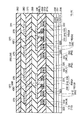
次に、2Trフラッシュメモリ3の備えるメモリセルアレイ10の平面構造について、図7乃至図11を用いて説明する。図7はメモリセルアレイ10の一部領域の平面図である。また図8乃至図11は、素子領域、ワード線、及びセレクトゲート線に加えて、それぞれ第1層目乃至第4層目の金属配線層の平面パターンを示した平面図であり、図示する領域は図7に対応している。
Next, the planar structure of the
図7乃至図11に示すように、半導体基板(p型ウェル領域)200中に、第1方向に沿ったストライプ形状の素子領域AAが、第1方向に直交する第2方向に沿って複数形成されている。そして、複数の素子領域AAを跨ぐようにして、第2方向に沿ったストライプ形状のワード線WL0〜WL(4m−1)が形成されている。またプライムセルアレイPCA内では、セレクトゲート線SG0〜SG(4m−1)がワード線WL0〜WL(4m−1)に平行に形成され、レプリカセルアレイRCA内では、レプリカセレクトゲート線RSG0〜RSG(4m−1)がワード線WL0〜WL(4m−1)に平行に形成されている。ワード線WL0〜WL(4m−1)がプライムセルアレイPCA及びレプリカセルアレイRCA間で電気的に共通接続されているのに対し、セレクトゲート線SG0〜SG(4m−1)とレプリカセレクトゲート線RSG0〜RSG(4m−1)とは電気的に分離されている。そして、ワード線WL0〜WL(4m−1)と素子領域AAとが交差する領域には、メモリセルトランジスタMTが形成されている。他方、セレクトゲート線SG0〜SG(4m−1)と素子領域AAとが交差する領域、及びレプリカセレクトゲート線RSG0〜RSG(4m−1)と素子領域AAとが交差する領域には、選択トランジスタSTが形成されている。また、ワード線WL0〜WL(4m−1)と素子領域AAとが交差する領域には、メモリセルトランジスタMT毎に分離されたフローティングゲート(図示せず)が形成されている。選択トランジスタSTは、メモリセルトランジスタMT同様に、制御ゲート及びフローティングゲートを有している。しかし、メモリセルトランジスタMTと異なり、選択トランジスタSTのフローティングゲートは、第2方向に沿って隣接する選択トランジスタST同士で共通接続されている。なお、隣接するプライムセル同士は、セレクトゲート線SGまたはワード線WL同士が隣り合っている。また隣接するレプリカセル同士は、レプリカセレクトゲート線RSGまたはワード線WL同士が隣り合っている。 As shown in FIGS. 7 to 11, a plurality of stripe-shaped element regions AA along the first direction are formed in the semiconductor substrate (p-type well region) 200 along the second direction orthogonal to the first direction. Has been. Then, stripe-shaped word lines WL0 to WL (4m−1) are formed along the second direction so as to straddle the plurality of element regions AA. In the prime cell array PCA, select gate lines SG0 to SG (4m-1) are formed in parallel to the word lines WL0 to WL (4m-1). In the replica cell array RCA, the replica select gate lines RSG0 to RSG (4m -1) is formed in parallel to the word lines WL0 to WL (4m-1). The word lines WL0 to WL (4m−1) are electrically connected in common between the prime cell array PCA and the replica cell array RCA, while the select gate lines SG0 to SG (4m−1) and the replica select gate lines RSG0 to RSG0. It is electrically separated from RSG (4m-1). A memory cell transistor MT is formed in a region where the word lines WL0 to WL (4m−1) and the element region AA intersect. On the other hand, in the region where the select gate lines SG0 to SG (4m−1) and the element region AA intersect, and the region where the replica select gate lines RSG0 to RSG (4m−1) and the element region AA intersect, the selection transistor ST is formed. A floating gate (not shown) separated for each memory cell transistor MT is formed in a region where the word lines WL0 to WL (4m−1) and the element region AA intersect. Like the memory cell transistor MT, the select transistor ST has a control gate and a floating gate. However, unlike the memory cell transistor MT, the floating gates of the selection transistors ST are commonly connected between the selection transistors ST adjacent in the second direction. Note that adjacent prime cells have adjacent select gate lines SG or word lines WL. Adjacent replica cells have adjacent replica select gate lines RSG or word lines WL.
以降、プライムセルアレイPCA内において、4列の素子領域AA群を、第1素子領域群AAG1と呼ぶことにする。そして、隣接する第1素子領域群AAG1間において、1列の素子領域AAが形成されている領域をソースコンタクト領域SCAと呼ぶことにする。第1素子領域群AAG1内に形成されるメモリセルMCは、データの記憶用として用いられる。しかし、ソースコンタクト領域SCA内のメモリセルMCは、ダミーのメモリセルであって、データの記憶用としては用いられない。また、2列の第1素子領域群AAG1毎に、スティッチ領域SA1が形成されている。本実施例ではスティッチ領域SA1内には素子領域AAは形成されない。またスティッチ領域SA1の幅は、1本の素子領域AAと、各素子領域AA間に形成された素子分離領域STIとを加えた幅に等しい。なおスティッチ領域SA1上にも、ワード線WL0〜WL(4m−1)及びセレクトゲート線SG0〜SG(4m−1)は形成されている。しかし、スティッチ領域SA1内に存在するワード線WL0〜WLm及びセレクトゲート線SG0〜SG(4m−1)は、実質的にプライムセルを構成するものではない。また、スティッチ領域SA1において、セレクトゲート線SG0〜SG(4m−1)は、その一部が幅広に形成されている。特に、隣接するセレクトゲート線側に凸となるように形成されている。この領域を、以後シャント領域SA2と呼ぶことにする。シャント領域SA2は、セレクトゲート線SG0〜SG(4m−1)に対して交互に設けられている。すなわち、あるスティッチ領域SA1においては、セレクトゲート線SG0、SG2、SG4…についてシャント領域SA2が形成され、当該スティッチ領域に隣接する別のスティッチ領域SA1においては、セレクトゲート線SG1、SG3、SG5、…についてシャント領域SA2が形成されている。そして、シャント領域SA2が形成されないセレクトゲート線は、当該スティッチ領域SA1において、その一部が除去されている。なお、以下では第1素子領域群AAG1とソースコンタクト領域SCAとを合わせた領域を第2素子領域群AAG2と呼ぶことにする。 Hereinafter, in the prime cell array PCA, a group of four element regions AA is referred to as a first element region group AAG1. A region in which one row of device regions AA is formed between adjacent first device region groups AAG1 is referred to as a source contact region SCA. The memory cells MC formed in the first element region group AAG1 are used for data storage. However, the memory cell MC in the source contact area SCA is a dummy memory cell and is not used for storing data. Further, a stitch region SA1 is formed for each of the two first element region groups AAG1. In this embodiment, the element region AA is not formed in the stitch region SA1. The width of the stitch region SA1 is equal to the width obtained by adding one element region AA and the element isolation region STI formed between the element regions AA. Note that word lines WL0 to WL (4m-1) and select gate lines SG0 to SG (4m-1) are also formed on the stitch region SA1. However, the word lines WL0 to WLm and select gate lines SG0 to SG (4m−1) existing in the stitch region SA1 do not substantially constitute a prime cell. In the stitch region SA1, some of the select gate lines SG0 to SG (4m−1) are formed wide. In particular, it is formed to be convex toward the adjacent select gate line. This region is hereinafter referred to as a shunt region SA2. The shunt region SA2 is alternately provided for the select gate lines SG0 to SG (4m-1). That is, in one stitch region SA1, a shunt region SA2 is formed for select gate lines SG0, SG2, SG4..., And in another stitch region SA1 adjacent to the stitch region, select gate lines SG1, SG3, SG5,. A shunt region SA2 is formed. A part of the select gate line in which the shunt region SA2 is not formed is removed in the stitch region SA1. In the following, a region including the first element region group AAG1 and the source contact region SCA is referred to as a second element region group AAG2.
また、レプリカセルアレイRCA内において、4列の素子領域AA群を、第3素子領域群AAG3と呼ぶことにする。そして、第3素子領域群AAG3に隣接し、1本の素子領域AAを含む領域をスティッチ領域SA3と呼ぶことにする。なおスティッチ領域SA3上にも、ワード線WL0〜WL(4m−1)及びレプリカセレクトゲート線RSG0〜RSG(4m−1)は形成されている。しかし、スティッチ領域SA3内に存在するワード線WL0〜WLm及びレプリカセレクトゲート線RSG0〜RSG(4m−1)は、実質的にレプリカセルを構成するものではない。スティッチ領域SA3では、スティッチ領域SA1と同様に、レプリカセレクトゲート線RSG0〜RSG(4m−1)が、その一部が幅広になるよう形成されている。特に、隣接するセレクトゲート線側に凸となるように形成されている。この領域を、以後シャント領域SA4と呼ぶことにする。 In the replica cell array RCA, a group of four element regions AA is referred to as a third element region group AAG3. A region adjacent to the third element region group AAG3 and including one element region AA is referred to as a stitch region SA3. Note that word lines WL0 to WL (4m−1) and replica select gate lines RSG0 to RSG (4m−1) are also formed on the stitch region SA3. However, the word lines WL0 to WLm and the replica select gate lines RSG0 to RSG (4m−1) existing in the stitch region SA3 do not substantially constitute a replica cell. In the stitch region SA3, like the stitch region SA1, the replica select gate lines RSG0 to RSG (4m−1) are formed so that a part thereof is wide. In particular, it is formed to be convex toward the adjacent select gate line. This region is hereinafter referred to as a shunt region SA4.
次に、図7及び図8を用いて、ワード線WL0〜WL(4m−1)、セレクトゲート線SG0〜SG(4m−1)、及びレプリカセレクトゲート線RSG0〜RSG(4m−1)の上に存在する1層目の金属配線層のパターンについて説明する。なお図8においては斜線を付した領域が、1層目の金属配線層である。 Next, referring to FIG. 7 and FIG. 8, above the word lines WL0 to WL (4m-1), the select gate lines SG0 to SG (4m-1), and the replica select gate lines RSG0 to RSG (4m-1). The pattern of the first metal wiring layer present in FIG. In FIG. 8, the hatched area is the first metal wiring layer.
まずプライムセルアレイPCA内の構成について説明する。図示するように、隣接するセレクトゲート線SG間(SG0〜SG1間、SG2〜SG3間、…)には、それぞれ第2方向に沿ったストライプ形状の金属配線層210が形成されている。金属配線層210は、プライムセルアレイPCAのソース線SLの一部となるものである。金属配線層210の長手方向(第2方向)は、スティッチ領域SA1で分離されている。すなわち、第2素子領域群AAG2毎に独立した形状を有している。そして金属配線層210は、プライムセルの選択トランジスタSTのソース領域とコンタクトプラグCP1により接続されている。本実施例では、ソースコンタクト領域SCA内ではコンタクトプラグCP1は形成されておらず、金属配線層210とソースコンタクト領域SCAにおけるメモリセルのソース領域とは電気的に接続されない。また、第1素子領域群AAG1内のメモリセルトランジスタMTのドレイン領域上には、島状のパターンの金属配線層220が形成されている。各金属配線層220は互いに分離されており、対応するメモリセルトランジスタMTのドレイン領域とコンタクトプラグCP2により接続されている。従って、第2方向に沿って並んだ複数の金属配線層220群と、第2方向に沿ったストライプ形状の金属配線層210とが、第1方向に沿って交互に配置された格好となっている。更に、シャント領域SA2上には、島状のパターンの金属配線層230が形成されている。そして、対応するセレクトゲート線SGのシャント領域SA2と、コンタクトプラグCP3により接続されている。金属配線層230は、第1方向に沿っては、対応するセレクトゲート線SGの上部から対応するワード線WLの上部にかけて延設されている。
First, the configuration in the prime cell array PCA will be described. As shown in the figure, between the adjacent select gate lines SG (between SG0 and SG1, between SG2 and SG3,...), A stripe-shaped
次にレプリカセルアレイRCA内の構成について説明する。図示するように、隣接するレプリカセレクトゲート線RSG間(RSG0〜RSG1間、RSG1〜RSG2間、…)には、それぞれ第2方向に沿ったストライプ形状の金属配線層210が形成されている。金属配線層210は、レプリカセルアレイRCAのソース線SLの一部となる。そして金属配線層210は、レプリカセルの選択トランジスタSTのソース領域とコンタクトプラグCP1により接続されている。また、プライムセルアレイPCAと同様にして、第3素子領域群AAG3内のメモリセルトランジスタMTのドレイン領域上に、島状のパターンの金属配線層220が形成されている。金属配線層220は、対応するメモリセルトランジスタMTのドレイン領域とコンタクトプラグCP2により接続されている。また、スティッチ領域SA3内には、金属配線層210と分離された金属配線層400が形成されている。金属配線層400は、レプリカセレクトゲート線RSG0〜RSG(4m−1)のシャント領域SA4とコンタクトプラグCP3により接続され、更にコンタクトプラグCP8によって素子領域AAに接続されている。
Next, the configuration in the replica cell array RCA will be described. As shown in the drawing, between the adjacent replica select gate lines RSG (between RSG0 to RSG1, between RSG1 and RSG2,...), Stripe-shaped metal wiring layers 210 are formed along the second direction. The
次に、図7及び図9を用いて、1層目の金属配線層210〜230、400の上に存在する2層目の金属配線層のパターンについて説明する。なお図9においては斜線を付した領域が、2層目の金属配線層である。 Next, the pattern of the second metal wiring layer existing on the first metal wiring layers 210 to 230 and 400 will be described with reference to FIGS. In FIG. 9, the hatched area is the second metal wiring layer.
図示するように、第1素子領域群AAG1及び第3素子領域群AAG3内においては、素子領域AA上に、第1方向に沿ったストライプ形状の金属配線層240が形成されている。金属配線層240は、ローカルビット線LBL0、LBL1として機能するものであり、コンタクトプラグCP4によって、第1層目の金属配線層220と接続されている。また、ソースコンタクト領域SCAにおいても、金属配線層240と同様のパターンの金属配線層250が形成されている。従って、金属配線層250の線幅は、金属配線層240と同一である。そして金属配線層250は、ソース線SLの一部として機能するものであり、コンタクトプラグCP5によって、第1層目の金属配線層210と接続されている。すなわち、第1方向で分離されている複数の金属配線層210が、金属配線層250によって共通接続されている。また、スティッチ領域SA1においては、島状のパターンの金属配線層260が形成されている。金属配線層260は、第1層目の金属配線層230に対応して形成されており、その形状は、金属配線層230と略同一のパターンを有しており、金属配線層230とオーバーラップしている。また、金属配線層260は、コンタクトプラグCP6によって、金属配線層230と接続されている。なお図7及び図9では、コンタクトプラグCP6はワード線WLの直上に位置しているが、金属配線層230と260とを接続できる位置で有れば限定されるものではない。
As shown in the drawing, in the first element region group AAG1 and the third element region group AAG3, a stripe-shaped
次に、図7及び図10を用いて、2層目の金属配線層240〜260の上に存在する3層目の金属配線層のパターンについて説明する。なお図10においては斜線を付した領域が3層目の金属配線層である。 Next, the pattern of the third metal wiring layer existing on the second metal wiring layers 240 to 260 will be described with reference to FIGS. In FIG. 10, the hatched area is the third metal wiring layer.
図示するように、第2方向に沿ったストライプ形状の金属配線層270が形成されている。金属配線層270は、1組のワード線及びセレクトゲート線毎(WL0とSG1の1組、WL1とSG1の1組、…毎)に設けられている。そして、対応するセレクトゲート線に電気的に接続されている第2層目の金属配線層260と、コンタクトプラグCP7によって接続されている。すなわち、各金属配線層270は、セレクトゲート線SG0〜SG(4m−1)のシャント配線として機能する。また、金属配線層270は、ワード線WLの中央部と、該ワード線WLに対応するセレクトゲート線SGの中央部との間の領域に形成されている。換言すれば、メモリセルMCの中央部を通過する。従って、複数の金属配線層270は、第1方向に沿った互いの間隔が、等間隔となるよう配置されている。そして、金属配線層270は、第2方向で隣接する第2素子領域群AAG2間で共通接続されている。金属配線層270の一端はセレクトゲートデコーダ30に接続され、他端は、レプリカセルアレイRCA上を通過して書き込み用デコーダ20に接続されている。
As illustrated, a stripe-shaped
次に、図7及び図11を用いて、3層目の金属配線層270の上に存在する4層目の金属配線層のパターンについて説明する。なお図11においては斜線を付した領域が4層目の金属配線層である。
Next, the pattern of the fourth metal wiring layer existing on the third
図示するように、第1方向に沿ったストライプ形状の金属配線層280、290が形成されている。金属配線層280は、書き込み用グローバルビット線WGBL0〜WGBL(2n−1)、及びレプリカ書き込み用グローバルビット線R_WGBL0、R_WGBL1として機能する。また金属配線層290は、読み出し用グローバルビット線RGBL0〜RGBL(n−1)、及びレプリカ読み出し用グローバルビット線R_RGBLとして機能する。そして、2本の金属配線層280と1本の金属配線層290で一組を為している。金属配線層280は、2本のローカルビット線LBL0、LBL1の一組、または2本のローカルビット線LBL2、LBL3の一組に対応して設けられ、金属配線層290は、4本のローカルビット線LBL0〜LBL3の一組に対応して設けられている。
As illustrated, striped metal wiring layers 280 and 290 are formed along the first direction. The
なお、上記図面において、レプリカセルアレイRCA内にソースコンタクトエリアSCAを設けても良い。 In the drawing, a source contact area SCA may be provided in the replica cell array RCA.
次に、上記構成のフラッシュメモリの断面構造について説明する。まず、プライムセルアレイPCAにおける第2素子領域群AAG2の断面構造について、図12乃至図18を用いて説明する。図12乃至図16はそれぞれ、図7におけるX1−X1’線方向、X2−X2’線方向、X3−X3’線方向、X4−X4’線方向、X5−X5’線方向に沿った断面図であり、図17、図18はそれぞれ、図7におけるY1−Y1’線、Y2−Y2’線に沿った断面図である。 Next, a cross-sectional structure of the flash memory having the above configuration will be described. First, the cross-sectional structure of the second element region group AAG2 in the prime cell array PCA will be described with reference to FIGS. 12 to 16 are cross-sectional views along the X1-X1 ′ line direction, the X2-X2 ′ line direction, the X3-X3 ′ line direction, the X4-X4 ′ line direction, and the X5-X5 ′ line direction in FIG. 17 and 18 are cross-sectional views taken along lines Y1-Y1 ′ and Y2-Y2 ′ in FIG. 7, respectively.
図示するように、p型半導体基板200の表面領域内にn型ウェル領域201が形成され、n型ウェル領域201の表面領域内にp型ウェル領域202が形成されている。p型ウェル領域202中には素子分離領域STIが形成され、素子分離領域STIによって周囲を取り囲まれた領域が、素子領域AAとなっている。p型ウェル領域201の素子領域AA上には、ゲート絶縁膜300が形成され、ゲート絶縁膜300上に、メモリセルトランジスタMT及び選択トランジスタSTのゲート電極が形成されている。メモリセルトランジスタMT及び選択トランジスタSTのゲート電極は、ゲート絶縁膜300上に形成された多結晶シリコン層310、多結晶シリコン層310上に形成されたゲート間絶縁膜320、及びゲート間絶縁膜320上に形成された多結晶シリコン層330を有している。ゲート間絶縁膜320は、例えばシリコン酸化膜、またはシリコン酸化膜とシリコン窒化膜との積層構造であるON膜、NO膜、またはONO膜で形成される。
As shown in the figure, an n-
メモリセルトランジスタMTにおいては、図12、図15に示すように、多結晶シリコン層310は隣接する素子領域AA間で互いに分離されており、フローティングゲート(FG)として機能する。他方、多結晶シリコン層330は、隣接する素子領域AA間で共通接続され、コントロールゲート(ワード線WL)として機能する。
In the memory cell transistor MT, as shown in FIGS. 12 and 15, the polycrystalline silicon layers 310 are separated from each other between adjacent element regions AA and function as floating gates (FG). On the other hand, the
選択トランジスタSTにおいては、図13、図14に示すように、多結晶シリコン膜310、320は、隣接する素子領域AA間で共通接続されている。そして、多結晶シリコン層310、330が、セレクトゲート線SGとして機能する。但し、実質的にセレクトゲート線として機能するのは、多結晶シリコン層310のみである(詳細は後述する)。
In the select transistor ST, as shown in FIGS. 13 and 14, the
そして隣接するゲート電極間に位置するp型ウェル領域202表面内には、不純物拡散層340が形成されている。不純物拡散層340は、隣接するトランジスタ同士で共用されている。
An
前述の通り、メモリセルトランジスタMTと選択トランジスタSTとを含むプライムセルPCは、次のような関係を有して形成されている。すなわち、隣接するプライムセルPCは、互いに選択トランジスタST同士、またはメモリセルトランジスタMT同士が隣り合っている。そして、隣り合ったもの同士は不純物拡散層340を共有している。従って、隣接する2つのプライムセルPC、PCは、選択トランジスタST同士が隣り合う場合には、2つの選択トランジスタST、STが共有する不純物拡散層340を中心にして、対称に配置されている。逆に、メモリセルトランジスタMT同士が隣り合う場合には、2つのメモリセルトランジスタMT、MTが共有する不純物拡散層340を中心にして、対称に配置されている。
As described above, the prime cell PC including the memory cell transistor MT and the selection transistor ST is formed with the following relationship. That is, in the adjacent prime cells PC, the select transistors ST or the memory cell transistors MT are adjacent to each other. Adjacent ones share the
そして、p型ウェル領域202上には、上記メモリセルトランジスタMT、及び選択トランジスタSTを被覆するようにして、層間絶縁膜350が形成されている。層間絶縁膜350中には、2つの選択トランジスタST、STが共有する不純物拡散層(ソース領域)340に達するコンタクトプラグCP1が形成されている。そして層間絶縁膜350上には、コンタクトプラグCP1に接続される金属配線層210が形成されている。金属配線層210は、ソース線SLとして機能する。また、層間絶縁膜350中には、2つのメモリセルトランジスタMT、MTが共有する不純物拡散層(ドレイン領域)340に達するコンタクトプラグCP2が形成されている。そして層間絶縁膜350上には、コンタクトプラグCP2に接続される金属配線層220が形成されている。
On the p-
層間絶縁膜350上には、金属配線層210、220を被覆するようにして、層間絶縁膜360が形成されている。そして、層間絶縁膜360中には、金属配線層220に達するコンタクトプラグCP4が形成されている(図17参照)。そして、層間絶縁膜360上には、複数のコンタクトプラグCP4に共通に接続された金属配線層240が形成されている(図17参照)。金属配線層240は、ローカルビット線LBL0〜LBL3のいずれかとして機能する。また層間絶縁膜360内には金属配線層210に達するコンタクトプラグCP5が形成されている(図18参照、ソースコンタクト領域SCA)。そして、層間絶縁膜360上には、複数のコンタクトプラグCP5をビット線方向で共通接続する金属配線層250が形成されている(図18参照、ソースコンタクト領域SCA)。金属配線層250は、ソース線SLの一部として機能する。
On the
層間絶縁膜360上には、金属配線層240、250を被覆するようにして、層間絶縁膜370が形成されている。そして、層間絶縁膜370上には金属配線層270が形成されている。金属配線層270は、セレクトゲート線のシャント配線として機能するものであり、配線間は等間隔とされている。そして、層間絶縁膜370上には、金属配線層270を被覆するようにして、層間絶縁膜380が形成されている。
An interlayer insulating
層間絶縁膜380上には、書き込み用グローバルビット線及び読み出し用グローバルビット線として機能する金属配線層280、290が形成され、更に層間絶縁膜390が形成されている。
On the
次に、プライムセルアレイ内のスティッチ領域SA1の断面構造について、図13、図16及び図19を用いて説明する。図19は図7におけるY3−Y3’線に沿った断面図である。 Next, the cross-sectional structure of the stitch region SA1 in the prime cell array will be described with reference to FIG. 13, FIG. 16, and FIG. 19 is a cross-sectional view taken along line Y3-Y3 'in FIG.
図示するように、p型ウェル領域202中には素子分離領域STIが形成されている。そして、素子分離領域STI上に、メモリセルトランジスタMTのフローティングゲート310及びコントロールゲート330が形成されている。また、当該スティッチ領域SA1においてシャント領域SA2を有しないセレクトゲート線は、多結晶シリコン層310、330が除去されている(図13参照)。すなわち、スティッチ領域SA1を挟んで、セレクトゲート線が分割されている。シャント領域SA2を有するセレクトゲート線は、当該スティッチ領域内においても、多結晶シリコン層310、330を含む積層ゲートが形成されている。そしてその積層ゲートは、隣接するセレクトゲート線に対して凸となるように形成されている(図19参照)。更に、図16及び図19に示すように、シャント領域SA2内においては、多結晶シリコン層330及びゲート間絶縁膜320が除去されて、多結晶シリコン層310が露出されている。そして、当該領域における多結晶シリコン層310上に接するようにして、コンタクトプラグCP3が形成されている。コンタクトプラグCP3と多結晶シリコン層330との間は、絶縁膜331によって電気的に分離されている(図16、図19参照)。コンタクトプラグCP3は、層間絶縁膜350表面から、多結晶シリコン層310に達するようにして形成される。
As illustrated, an element isolation region STI is formed in the p-
層間絶縁膜350上には、金属配線層230が形成されている。金属配線層230は、対応する選択トランジスタSTのゲート電極上部を被覆し、且つ、当該選択トランジスタに対応するメモリセルトランジスタMTの積層ゲート電極上部を被覆するように延設されている(図19参照)。そして、対応する選択トランジスタSTに接続されたコンタクトプラグCP3に接続されている。層間絶縁膜350上には、金属配線層230を被覆するようにして層間絶縁膜360が形成されている。層間絶縁膜360中には、金属配線層230に達するコンタクトプラグCP6が形成され、層間絶縁膜360上にはコンタクトプラグCP6と接続される金属配線層260が形成されている。金属配線層260も金属配線層230と同様に、対応する選択トランジスタSTのゲート電極上部を被覆し、且つ、当該選択トランジスタSTに対応するメモリセルトランジスタMTの積層ゲート電極上部を被覆するように延設されている(図19参照)。層間絶縁膜360上には層間絶縁膜370が形成され、層間絶縁膜370中には金属配線層260に達するコンタクトプラグCP7が形成されている。図19に示すように、コンタクトプラグCP7は、メモリセルの中央部に位置している。換言すれば、メモリセルトランジスタMTの積層ゲートの中央部と、選択トランジスタSTのゲート電極の中央部との間の領域上に形成されている。層間絶縁膜370上には、コンタクトプラグCP7と接続された金属配線層270が形成されている。図19に示されるように、複数の金属配線層270は、層間絶縁膜370上に等間隔に配置されている。そして、層間絶縁膜370上に、金属配線層270を被覆するようにして層間絶縁膜380、390が形成されている。
A
図20は、シャント領域SA2の斜視図である。図示するように、セレクトゲート線を形成する積層ゲート構造が、一部幅広に形成されている。そして、幅広に形成された領域の一部における多結晶シリコン層330及びゲート間絶縁膜320が除去されて、多結晶シリコン層310が露出されている。この露出された多結晶シリコン層310に接触するようにして、コンタクトプラグCP3が形成されている。更に、コンタクトプラグCP3は、多結晶シリコン層330と電気的に分離されている。すなわち、多結晶シリコン層330は、シャント配線270とは電気的に分離されている。
FIG. 20 is a perspective view of the shunt region SA2. As shown in the drawing, the laminated gate structure for forming the select gate line is partially formed wide. Then, the
次に、レプリカセルアレイRCAについて説明する。まず、レプリカセルアレイRCAおける第3素子領域群AAG3の断面構造について、図21及び図22を用いて説明する。図21及び図22はそれぞれ、図7におけるX6−X6’線方向、Y4−Y4’線方向に沿った断面図である。 Next, the replica cell array RCA will be described. First, the cross-sectional structure of the third element region group AAG3 in the replica cell array RCA will be described with reference to FIGS. 21 and 22 are cross-sectional views along the X6-X6 'line direction and the Y4-Y4' line direction in FIG. 7, respectively.
図示するように、第3素子領域群AAG3の構成は、プライムセルアレイPCAにおける第1素子領域群と同じである。すなわち、p型ウェル領域202中に素子分離領域STIが形成され、素子分離領域STIによって周囲を取り囲まれた領域が、素子領域AAとなっている。p型ウェル領域201の素子領域AA上には、ゲート絶縁膜300が形成され、ゲート絶縁膜300上に、レプリカセルRCのメモリセルトランジスタMT及び選択トランジスタSTのゲート電極が形成されている。
As shown in the figure, the configuration of the third element region group AAG3 is the same as that of the first element region group in the prime cell array PCA. That is, the element isolation region STI is formed in the p-
メモリセルトランジスタMTにおいては、多結晶シリコン層310は隣接する素子領域AA間で互いに分離されており、フローティングゲート(FG)として機能する。他方、多結晶シリコン層330は、隣接する素子領域AA間で共通接続され、コントロールゲート(ワード線WL)として機能する。
In the memory cell transistor MT, the
選択トランジスタSTにおいては、多結晶シリコン膜310、320は、隣接する素子領域AA間で共通接続されている。そして、多結晶シリコン層310、330が、レプリカセレクトゲート線RSGとして機能する。但し、実質的にレプリカセレクトゲート線として機能するのは、多結晶シリコン層310のみである。
In the select transistor ST, the
メモリセルトランジスタのコントロールゲートとなる多結晶シリコン層330は、プライムセルPCのコントロールゲートと共通接続されている。他方、レプリカセルRCのレプリカセレクトゲート線RSGとなる多結晶シリコン層310、330は、プライムセルアレイPCAとレプリカセルアレイRCAとの境界部分において、プライムセルPCのセレクトゲート線SGとなる多結晶シリコン層310、330と分離されている。
The
そして隣接するゲート電極間に位置するp型ウェル領域202表面内には、不純物拡散層340が形成されている。不純物拡散層340は、隣接するトランジスタ同士で共用されている。
An
前述の通り、メモリセルトランジスタMTと選択トランジスタSTとを含むレプリカセルRCは、次のような関係を有して形成されている。すなわち、隣接するレプリカセルRCは、互いに選択トランジスタST同士、またはメモリセルトランジスタMT同士が隣り合っている。そして、隣り合ったもの同士は不純物拡散層340を共有している。従って、隣接する2つのレプリカセルRC、RCは、選択トランジスタST同士が隣り合う場合には、2つの選択トランジスタST、STが共有する不純物拡散層340を中心にして、対称に配置されている。逆に、メモリセルトランジスタMT同士が隣り合う場合には、2つのメモリセルトランジスタMT、MTが共有する不純物拡散層340を中心にして、対称に配置されている。
As described above, the replica cell RC including the memory cell transistor MT and the selection transistor ST is formed with the following relationship. That is, in the adjacent replica cells RC, the select transistors ST or the memory cell transistors MT are adjacent to each other. Adjacent ones share the
層間絶縁膜360上には、セレクトゲート線SGのシャント配線270が形成されている。しかし、シャント配線270と、レプリカセレクトゲート線RSGとなる多結晶シリコン層310、330とは電気的に分離されている。そして層間絶縁膜380上には、レプリカ書き込み用グローバルビット線及びレプリカ読み出し用グローバルビット線として機能する金属配線層280、290が形成されている。
On the
次に、レプリカセルアレイRCA内のスティッチ領域SA3の断面構造について、図21及び図23を用いて説明する。図23は図7におけるY5−Y5’線に沿った断面図である。 Next, the cross-sectional structure of the stitch region SA3 in the replica cell array RCA will be described using FIG. 21 and FIG. 23 is a cross-sectional view taken along line Y5-Y5 'in FIG.
図示するように、スティッチ領域SA3内には、レプリカセレクトゲート線RSG0〜RSG(4m−1)のシャント領域SA4及び素子領域AAが形成されている。シャント領域SA4の構造は、セレクトゲート線SGのシャント領域SA2と同じである(図20、図23参照)。すなわち、レプリカセレクトゲート線RSGの一部である多結晶シリコン層330及びゲート間絶縁膜320が除去されて、多結晶シリコン層310が露出されている。そして、当該領域における多結晶シリコン層310上に接するようにして、コンタクトプラグCP3が形成されている。コンタクトプラグCP3と多結晶シリコン層330との間は、絶縁膜331によって電気的に分離されている。コンタクトプラグCP3は、層間絶縁膜350表面から、多結晶シリコン層310に達するようにして形成される。
As illustrated, a shunt region SA4 and an element region AA of the replica select gate lines RSG0 to RSG (4m−1) are formed in the stitch region SA3. The structure of the shunt region SA4 is the same as that of the shunt region SA2 of the select gate line SG (see FIGS. 20 and 23). That is, the
また、スティッチ領域SA3内には素子領域AAが形成されており、層間絶縁膜350内には、素子領域AAに達するコンタクトプラグCP8が形成されている(図21参照)。層間絶縁膜350上には、金属配線層400が形成されている。金属配線層400は、コンタクトプラグCP3とコンタクトプラグCP8とを接続する。すなわち、レプリカセレクトゲート線RSGとなる多結晶シリコン層310は、コンタクトプラグCP3、CP8、及び金属配線層400を介在して、p型ウェル領域202に接続されている。
An element region AA is formed in the stitch region SA3, and a contact plug CP8 reaching the element region AA is formed in the interlayer insulating film 350 (see FIG. 21). A
層間絶縁膜350上には層間絶縁膜360、370が順次形成され、層間絶縁膜370上に、シャント配線270が形成されている。また、スティッチ領域SA3内にもワード線WL0〜WL(4m−1)が形成されている。シャント配線270及びワード線WL0〜WL(4m−1)は、スティッチ領域SA3を通過して書き込み用デコーダ20に接続される。他方、レプリカセレクトゲート線RSG0〜RSG(4m−1)となる多結晶シリコン層310、330は、レプリカセルアレイRCA内にのみ形成されている。
次に、読み出し制御回路130内のディスチャージ回路131の備える電流源回路137の構成について、図24乃至図27を用いて説明する。図24は、電流源回路137の平面図であり、図25乃至図27はそれぞれ、図24におけるX7−X7’線方向、Y6−Y6’線方向、Y7−Y7’線方向に沿った断面図であり、
図示するように、メモリセルアレイ10と同様に、p型半導体基板200の表面内にn型ウェル領域201が形成され、n型ウェル領域201の表面内にp型ウェル領域202が形成されている。p型ウェル領域202の表面内には複数の素子分離領域STIが形成され、素子分離領域STIによって周囲を取り囲まれ、長手方向が第1方向に沿ったストライプ形状の領域が素子領域AAとなっている。また、p型ウェル領域202上には、複数の素子領域AAを跨ぐようにして、第1方向に直交する第2方向に沿ったストライプ形状のゲート電極410、420が形成されている。ゲート電極410、420はそれぞれ、MOSトランジスタ137−1、137−2のゲート電極として機能するものである。ゲート電極410、420は、プライムセルPC及びレプリカセルRCの選択トランジスタSTと同様のスタック構造を有している。すなわち、ゲート電極410は、p型ウェル領域202上にゲート絶縁膜411を介在して形成された多結晶シリコン層412と、多結晶シリコン層412上にゲート間絶縁膜413を介在して形成された多結晶シリコン層414とを備えている。そして、多結晶シリコン層412、414は、隣接する素子領域AA間で共通接続されている。但し、実質的にゲート電極として機能するのは多結晶シリコン層412である。そして、p型ウェル領域202の表面内に、MOSトランジスタ137−1、137−2のソース領域及びドレイン領域として機能する不純物拡散層480が形成されている。MOSトランジスタ137−1のソース領域は、MOSトランジスタ137−2のドレイン領域と、不純物拡散層430を共有する。
Next, the configuration of the
As shown in the figure, similarly to the
なお、複数の素子領域AA上に、複数のMOSトランジスタが形成されているが、MOSトランジスタ137−1、137−2として機能するのはそのうちのいずれかのみであり、その他のMOSトランジスタは、ダミーのMOSトランジスタであり、電流源回路137として実質的な機能を有するものではない。
Note that a plurality of MOS transistors are formed on the plurality of element regions AA, but only one of them functions as the MOS transistors 137-1 and 137-2. The MOS transistor does not have a substantial function as the
ゲート電極410、420は、電流源回路137の端部まで引き出され、プライムセルPCやレプリカセルRCのシャント領域SA2、SA4と同一の構造を有する領域が形成されている。すなわち、素子分離領域STI上において、ゲート電極410、420は幅広になるように形成され、多結晶シリコン層414、424及びゲート間絶縁膜413、423が除去されている。
The
そして、上記MOSトランジスタ群を被覆するようにして、p型ウェル領域202上に層間絶縁膜350が形成されている。層間絶縁膜350中には、MOSトランジスタ480の不純物拡散層480に達するコンタクトホールCP9、CP10が形成されている。コンタクトホールCP9は、MOSトランジスタ137−1のドレイン、及びMOSトランジスタ137−1と同一行にあるダミーMOSトランジスタのドレインに接続される。他方、コンタクトホールCP10は、MOSトランジスタ137−2のソース、及びMOSトランジスタ137−2と同一行にあるダミーMOSトランジスタのソースに接続される。更に、多結晶シリコン層414、424及びゲート間絶縁膜413、423が除去された領域においては、層間絶縁膜350中に、多結晶シリコン層412、422に達するコンタクトプラグCP11が形成されている。
An interlayer insulating
層間絶縁膜350上には、島状の金属配線層430が形成されている。互いに離隔された金属配線層430は、それぞれコンタクトプラグCP9またはCP10と接している。更に層間絶縁膜350上には、金属配線層470が、コンタクトプラグCP11に接続されるようにして形成されている。すなわち、ゲート電極410の多結晶シリコン層412と、ゲート電極420の多結晶シリコン層422とは、コンタクトプラグCP11及び金属配線層470を介在して、電気的に接続されている。
On the
層間絶縁膜350上には、上記金属配線層430、470を被覆するようにして層間絶縁膜360が形成されている。層間絶縁膜360中には、コンタクトプラグCP9に接続された金属配線層430に接するコンタクトプラグCP11、及びコンタクトプラグCP10に接続された金属配線層430に接するコンタクトプラグCP12が形成されている。
An interlayer insulating
層間絶縁膜360上には、長手方向が第1方向に沿ったストライプ形状の金属配線層440、450、460が形成されている。金属配線層440は、MOSトランジスタ137−1に電気的に接続されたコンタクトプラグCP11に接し、金属配線層450は、MOSトランジスタ137−2に電気的に接続されたコンタクトプラグCP12に接する。金属配線層460は、ダミーMOSトランジスタに接続されたコンタクトプラグCP11、CP12に接する。そして金属配線層440はレプリカ読み出し用グローバルビット線R_RGBLに接続され、金属配線層450は接地電位に接続されている。上記金属配線層440、450、460を被覆するようにして、層間絶縁膜360上には層間絶縁膜370が形成されている。
On the
上記のように、電流源回路137は、メモリセルアレイ10内のメモリセルブロックBLKと同様の構成を有しており、メモリセルブロックの一部を電流源回路137として流用出来る。この際、メモリセルトランジスタMT及び選択トランジスタSTは、それぞれ電流源回路137のMOSトランジスタ137−1、137−2のいずれかとして機能出来る。そして、メモリセルアレイ10内の金属配線層220及びローカルビット線を、それぞれ電流源回路137の金属配線層430及び金属配線層440、450、460として用いることが出来る。
As described above, the
次に、上記構成の2Trフラッシュメモリ3の動作について、図28を用いて以下説明する。図28は、各種信号及び各ノードの電圧のタイミングチャートである。なお以下では、フローティングゲートに電子が注入されておらず閾値電圧が負である状態を“1”データが書き込まれている状態、フローティングゲートに電子が注入され、閾値電圧が正である状態を“0”データが書き込まれている状態と定義する。また説明の簡単化の為に、2本の書き込み用グローバルビット線WGBL0、WGBL1及び1本の読み出し用グローバルビット線RGBL0を有するメモリセルアレイ10の場合を例に説明する。
Next, the operation of the
<初期動作>
まず、初期動作について図29を用いて説明する。初期動作とは、データの書き込み、読み出し、及び消去などにあたって、最初に行われる動作のことである。初期動作は、図28において、時刻t0〜t1の期間に行われる。図29は、初期動作時における、書き込み用グローバルビット線WGBL0、WGBL1に対応した入力バッファ90、スイッチ群80、及び書き込み回路50の回路図である。なお図29はプライムセルアレイに対応した図面であるが、レプリカセルアレイに対応する構成も同様である。
<Initial operation>
First, the initial operation will be described with reference to FIG. The initial operation is an operation that is first performed in writing, reading, and erasing data. The initial operation is performed in the period from time t0 to t1 in FIG. FIG. 29 is a circuit diagram of the
まず初期動作にあたっては、信号WDH0、WDH1が共に“L”レベル(0V)とされる。これによりスイッチ群80内のMOSトランジスタ81がオフ状態となり、書き込み回路50と入力バッファ90とは電気的に分離される。また、ラッチ回路53の高電圧電源電圧として与えられる書き込み禁止電圧VPIがVcc2とされ、VBLPWが0Vとされる。そして、信号WGBLRSTが“H”レベル(Vcc2)とされ、全ての書き込み用グローバルビット線WGBL0、WGBL1がリセットされる。すなわち、書き込み回路50内のMOSトランジスタ58がオン状態とされ、VBLPWノードから0Vが書き込み用グローバルビット線WGBL0、WGBL1に与えられる。この結果、全てのラッチ回路53の出力ノードは“L”レベル(0V)となり、入力ノード(ノードA0、A1)は“H”レベル(Vcc2)となる。
First, in the initial operation, the signals WDH0 and WDH1 are both set to the “L” level (0 V). As a result, the
以上のように、初期動作において、書き込み用グローバルビット線及びレプリカ書き込み用グローバルビット線が0Vにされると共に、ノードA0、A1にVcc2が与えられる。 As described above, in the initial operation, the write global bit line and the replica write global bit line are set to 0 V, and Vcc2 is applied to the nodes A0 and A1.
<データラッチ動作>
次に、データラッチ動作について図30及び図31を用いて説明する。データラッチ動作とは、データの書き込みにあたって、各ラッチ回路53に対して、書き込みデータを入力する動作のことである。データラッチ動作は、時刻t1〜t2の間に行われる。図30、図31はデータラッチ動作時における、入力バッファ90、スイッチ群80、及び書き込み回路50の回路図であり、図30は“0”データが入力された場合、図31は“1”データが入力された場合について示している。以下では、書き込み用グローバルビット線WGBL0に接続されたメモリセルに“0”データを書き込み(WGBL0が選択状態)、WGBL1に接続されたメモリセルに“1”データを書き込む(WGBL1が非選択状態)場合を例に挙げて説明する。
<Data latch operation>
Next, the data latch operation will be described with reference to FIGS. The data latch operation is an operation of inputting write data to each
まず図30を用いて“0”データが入力された際について説明する。データラッチ動作にあたっては、信号WGBLRSTが0Vとされ、MOSトランジスタ58はオフ状態とされる。これにより、各書き込み用グローバルビット線WGBL0、WGBL1はVBLPWノードと電気的に分離される。更に、書き込み用グローバルビット線WGBL0に対応するラッチ回路53にデータをラッチさせる為に、信号WDH0が“H”レベル(Vcc2)とされ、書き込み用グローバルビット線WGBL0に対応するMOSトランジスタ81がオン状態となる。他方、書き込み用グローバルビット線WGBL1に対応するMOSトランジスタ81はオフ状態となる。従って、入力バッファ90と、書き込み用グローバルビット線WGBL0に対応するラッチ回路53とが電気的に接続される。
First, a case where “0” data is input will be described with reference to FIG. In the data latch operation, the signal WGBLRST is set to 0V, and the
そして、CPU2から入力バッファ90のインバータに“0”データが入力される。“0”データが入力される際には、インバータ91の入力ノードに0Vが印加される。“0”データはインバータ91で反転される。その結果、TOWDI0ノードの電位はVcc2となる。すると、MOSトランジスタ82のゲートにはVcc2が印加されているので、MOSトランジスタ82はカットオフの状態となる。従って、ラッチ回路53は時刻t0〜t1で与えられたデータを保持し続ける。すなわち、ノードA0はVcc2のままであり、書き込み用グローバルビット線WGBL0は0Vのままである。
Then, “0” data is input from the
次に図31を用いて“1”データを入力する場合について説明する。“0”データを入力する場合と異なるのは、WDH0=0V、WDH1=Vcc2とされることにより、書き込み用グローバルビット線WGBL1に対応するMOSトランジスタ81がオン状態とされる点である。
Next, a case where “1” data is input will be described with reference to FIG. A difference from the case of inputting “0” data is that the
そしてCPU2から入力バッファに“1”データが入力される。“1”データが入力される際には、インバータ91の入力ノードにVcc2が印加される。従って、TOWDI0ノードの電位は0Vとなる。このTOWDI0ノードの電位は、MOSトランジスタ81の電流経路を介してラッチ回路53に入力される。その結果、ノードA1の電位はVcc2から0Vに反転し、書き込み用グローバルビット線WGBL1の電位は0VからVcc2に反転する。
Then, “1” data is input from the
以上のように、データラッチ動作においては、“1”書き込みを行うメモリセルに対応したラッチ回路内のデータが、初期状態から反転される。すなわち、“0”書き込み(電子を注入)するときには、実質的にはデータは外部から入力されず、“1”書き込み(電子を注入しない=非選択)するときには、データを外部から取り込む。 As described above, in the data latch operation, the data in the latch circuit corresponding to the memory cell to which “1” is written is inverted from the initial state. That is, when writing “0” (injecting electrons), data is not substantially input from the outside, and when writing “1” (does not inject electrons = not selected), data is taken in from the outside.
なお、2Trフラッシュメモリにデータをストアさせる際、レプリカセルの全ては書き込み非選択とされる。従って、レプリカ書き込み用グローバルビット線R_WGBL0、R_WGBL1に対応する書き込み回路50、スイッチ群80及び入力バッファ90の動作は、上記プライムセルアレイPCAにおける書き込み用グローバルビット線WGBL1の場合と同様である。すなわち、レプリカ書き込み用グローバルビット線R_WGBL0、R_WGBL1には、MOSトランジスタ52のソースからVPI=0Vが与えられる。
Note that when storing data in the 2Tr flash memory, all of the replica cells are unselected for writing. Therefore, the operations of the
<書き込み動作>
次に書き込み動作について図32を用いて説明する。データの書き込みは、同一行にある全てのメモリセルブロックに対して一括して行われる。但し、各メモリセルブロック内において、同時に書き込まれるメモリセルは、ローカルビット線LBL0、LBL1のいずれかに接続されたプライムセルと、ローカルビット線LBL2、LBL3のいずれかに接続されたプライムセルの2つである。また、選択ワード線に接続されたレプリカセルには、必ず“1”データが書き込まれる。言い換えれば、レプリカセルが保持しているデータは書き換えられない。
<Write operation>
Next, the write operation will be described with reference to FIG. Data writing is performed collectively for all memory cell blocks in the same row. However, in each memory cell block, two memory cells are simultaneously written: a prime cell connected to one of the local bit lines LBL0 and LBL1, and a prime cell connected to one of the local bit lines LBL2 and LBL3. One. In addition, “1” data is always written in the replica cell connected to the selected word line. In other words, the data held in the replica cell cannot be rewritten.
書き込み動作は、図28において、時刻t2〜t3の期間に行われる。また図31は、書き込み動作時におけるメモリセルアレイ10及び書き込み回路50の回路図である。図32において、ワード線WL0、及びローカルビット線LBL0、LBL2に接続されたメモリセルトランジスタMTにデータを書き込むものとし、そのうち、ローカルビット線LBL0に接続されたメモリセルトランジスタMTに“0”データを書き込み、ローカルビット線LBL2に接続されたメモリセルトランジスタMTに“1”データを書き込むものとする。換言すれば、ローカルビット線LBL0に接続されたメモリセルが選択され、ローカルビット線LBL2に接続されたメモリセルが非選択とされる。
The write operation is performed in the period from time t2 to t3 in FIG. FIG. 31 is a circuit diagram of the
まず書き込み動作にあたって、信号WGBLRSTは依然として0Vである。そして、時刻t2において書き込み禁止電圧VPIがVcc2から0Vに変化し、VBLPWノードの電位が0VからVBB1(−7V)に変化する。負電位VBB1は、ライトステートマシーン110の命令によって電圧発生回路120が出力する。なお、VPIの電位は、−7Vではなく、その他の負電位であっても良い。
First, in the write operation, the signal WGBLRST is still 0V. At time t2, the write inhibit voltage VPI changes from Vcc2 to 0V, and the potential of the VBLPW node changes from 0V to VBB1 (−7V). The negative potential VBB1 is output by the
すると、ラッチ回路53内のインバータ54、55の低電圧側の電源電圧が0VからVBB1に変化し、高電圧側の電源電圧がVcc2から0Vに変化するから、ノードA0、A1の電位はそれぞれ0V、VBB1に変化する。また書き込み用グローバルビット線WGBL0、WGBL1の電位もそれぞれVBB1、0Vに変化する。
Then, the power supply voltage on the low voltage side of the
そして、書き込み用デコーダ20が、ワード線WL0を選択して、選択ワード線WL0に正電圧VPP(12V)を印加する。また分離用MOSトランジスタ25がオン状態とされることによって、VSGPWノードから、全セレクトゲート線SG0〜SG(4m−1)に負電位VBB1(−7V)が印加される。更に、レベルシフト回路27の出力が“L”レベルとなり、VPW_RWノードが0VからVBB1に変化するから、メモリセルが形成されている基板(p型ウェル領域202)には負電位VBB1が印加される。なお、書き込み時においては、信号ZISOGは“L”レベルとされており、セレクトゲートデコーダ30のロウアドレスデコード回路31は、セレクトゲート線から電気的に分離されている。
Then, the
また、カラムデコーダ40は、選択ワード線WL0を含むメモリセルブロックBLKに対応する書き込み用カラムセレクタWCSに接続された2本の書き込み用カラム選択線のうち、書き込み用カラム選択線WCSL0を選択する。これにより、書き込み用カラムセレクタWCS内のMOSトランジスタ11、13がオン状態とされる。その結果、書き込み用グローバルビット線WGBL0とローカルビット線LBL0とが電気的に接続され、書き込み用グローバルビット線WGBL1とローカルビット線LBL2とが電気的に接続される。
The
またカラムデコーダ40は、選択ワード線WL0を含まないメモリセルブロックBLKに対応する書き込み用カラムセレクタWCSに接続された書き込み用カラム選択線を全て非選択とする。そのため、選択ワード線を含まないメモリセルブロックBLKに対応する書き込み用カラムセレクタWCS内のMOSトランジスタ11〜14はオフ状態とされる。
Further, the
更にカラムデコーダ40は、全ての読み出し用カラム選択線RCSL0〜RCSL(4m−1)を非選択とする。これにより、全ての読み出し用カラムセレクタRCS内のMOSトランジスタ15〜18はオフ状態とされる。従って、読み出し用グローバルビット線RGBLとローカルビット線LBL0〜LBL3とは、電気的に分離されている。
Further, the
更にカラムデコーダ40は、非選択とされるローカルビット線LBL1、LBL3に接続されるMOSトランジスタ42、44をオン状態とすべく、書き込み禁止用カラム選択線ICSL1を“H”レベル(Vcc2)とする。選択ローカルビット線LBL0、LBL2に対応するMOSトランジスタ41、43に接続される書き込み禁止用カラム選択線ICSL0は“L”レベルとされ、MOSトランジスタ41、43はオフ状態である。その結果、非選択ローカルビット線LBL1、LBL3には書き込み禁止電圧VPI=0Vが印加される。
Further, the
上記の結果、書き込み用カラムセレクタWCS内のMOSトランジスタ11を介して、書き込み用グローバルビット線WGBL0から、選択ワード線WL0を含むメモリセルブロックBLKのローカルビット線LBL0に、書き込み電圧(VBB1)が与えられる。更に、MOSトランジスタ13を介して、書き込み用グローバルビット線WGBL1から、選択ワード線WL0を含むメモリセルブロックBLKのローカルビット線LBL2に、書き込み禁止電圧VPI(0V)が与えられる。
As a result, the write voltage (VBB1) is applied from the write global bit line WGBL0 to the local bit line LBL0 of the memory cell block BLK including the selected word line WL0 via the
その結果、書き込み用グローバルビット線WGBL1及びワード線WL0に接続されたメモリセルトランジスタMTにおいては、ゲート・チャネル間の電位差が十分ではない(VPP−VPI=12V)ため、フローティングゲートに電子は注入されない。すなわち、メモリセルMCは負の閾値を維持する。すなわち“1”データが書き込まれる。また、非選択ローカルビット線LBL1、LBL3及びワード線WL0に接続されたメモリセルトランジスタMTにおいても、チャネルにVPIが印加されているため、フローティングゲートに電子は注入されず、メモリセルMCは負の閾値を保持する。他方、書き込み用グローバルビット線WGBL0及びワード線WL0に接続されたメモリセルトランジスタMTにおいては、ゲート・チャネル間の電位差が十分である(VPP−VBB1=19V)ため、FN tunnelingによってフローティングゲートに電子が注入される。その結果、メモリセルトランジスタMTの閾値は正に変化する、すなわち“0”データが書き込まれる。 As a result, in the memory cell transistor MT connected to the write global bit line WGBL1 and the word line WL0, the potential difference between the gate and the channel is not sufficient (VPP−VPI = 12V), so that electrons are not injected into the floating gate. . That is, the memory cell MC maintains a negative threshold value. That is, “1” data is written. In addition, in the memory cell transistor MT connected to the unselected local bit lines LBL1, LBL3 and the word line WL0, VPI is applied to the channel, so that electrons are not injected into the floating gate, and the memory cell MC is negative. Holds the threshold. On the other hand, in the memory cell transistor MT connected to the write global bit line WGBL0 and the word line WL0, the potential difference between the gate and the channel is sufficient (VPP−VBB1 = 19V). Injected. As a result, the threshold value of the memory cell transistor MT changes positively, that is, “0” data is written.
なお上記はプライムセルアレイPCAの場合であるが、レプリカセルアレイRCAの場合であっても同様である。但しレプリカセレクトゲート線RSG0〜RSG(4m−1)はVPWに接続されているため、全てVBB1とされる。そしてレプリカ書き込み用グローバルビット線R_WGBL0、R_WGBL1とワード線WL0に接続されたメモリセルトランジスタMTのフローティングゲートには電子は注入されない。従って、レプリカセルRCの閾値は負の値を維持する。 The above is the case of the prime cell array PCA, but the same applies to the case of the replica cell array RCA. However, since the replica select gate lines RSG0 to RSG (4m−1) are connected to the VPW, they are all set to VBB1. Electrons are not injected into the floating gates of the memory cell transistors MT connected to the replica write global bit lines R_WGBL0, R_WGBL1 and the word line WL0. Therefore, the threshold value of the replica cell RC maintains a negative value.
以上のようにして、1ページのメモリセルトランジスタに一括してデータが書き込まれる。そして、実質的にデータのストレージに用いられるのはプライムセルアレイPCAのみであり、レプリカセルアレイRCAには常時“0”データが書き込まれる。すなわち、書き込み動作によってレプリカセルRCの閾値は変化することは無く、レプリカセルRCには実質的にデータは書き込まれない。 As described above, data is written collectively to one page of memory cell transistors. Only the prime cell array PCA is substantially used for data storage, and “0” data is always written in the replica cell array RCA. That is, the threshold value of the replica cell RC is not changed by the write operation, and data is not substantially written to the replica cell RC.
<読み出し動作>
次に読み出し動作について図33、図34を用いて説明する。図33は、2Trフラッシュメモリ3のプライムセルアレイPCA及び読み出しユニット61の回路図であり、図34は、レプリカセルアレイRCA及び読み出し制御回路130の回路図である。図33は、ローカルビット線LBL0とワード線WL0に接続されたメモリセルトランジスタMTからデータを読み出す場合について示しており、図34はその際におけるレプリカセルアレイRCAの様子を示している。
<Read operation>
Next, the reading operation will be described with reference to FIGS. FIG. 33 is a circuit diagram of the prime cell array PCA and the
本実施形態においてデータはプライムセルアレイPCAのみから読み出され、レプリカセルアレイRCAからは読み出されない。そしてデータは、メモリセルブロックBLKあたり1つのプライムセルPCから読み出される。但し1つのメモリセルブロックBLKあたり複数本の読み出し用グローバルビット線が存在する場合には、その数だけデータが読み出される。 In the present embodiment, data is read only from the prime cell array PCA and not read from the replica cell array RCA. Data is read from one prime cell PC per memory cell block BLK. However, when there are a plurality of read global bit lines per memory cell block BLK, the data is read by that number.
まず図33に示すように、セレクトゲートデコーダ30が、セレクトゲート線SG0を選択(“H”レベル:Vcc=3V)する。また、書き込み用デコーダ20は、全てのワード線WL0〜WL(4m−1)を非選択(0V)とし、p型ウェル領域202の電位VPWを0Vとする。更に、ソース線ドライバ70は、ソース線の電位を0Vとする。
First, as shown in FIG. 33, the
そして、カラムデコーダ40は、選択セレクトゲート線SG0を含むメモリセルブロックBLKに対応する読み出し用カラムセレクタRCSに接続された、4本の読み出し用カラム選択線RCSL0〜RCSL3のうち、読み出し用カラム選択線RCSL0を選択する。これにより、選択セレクトゲート線SG0を含むメモリセルブロックBLKに対応する読み出し用カラムセレクタRCS内のMOSトランジスタ15がオン状態とされる。また、信号ISOが“H”レベルとされて、MOSトランジスタ72がオン状態となる。その結果、読み出し用グローバルビット線RGBL0と、ローカルビット線LBL0とが電気的に接続される。但し、選択セレクトゲート線SG0を含まないメモリセルブロックBLKに対応する読み出し用カラムセレクタRCSに接続される全ての読み出し用カラム選択線は非選択とされる。
Then, the
またカラムデコーダ40は、全ての書き込み用カラム選択線WCSL0〜WCSL(2m−1)を非選択とする。これにより、全ての書き込み用カラム選択線WCSL0〜WCSL(2m−1)内の4つのMOSトランジスタ11〜14の全てがオフ状態とされる。従って、書き込み用グローバルビット線WGBLとローカルビット線LBL0〜LBL3とは、電気的に分離されている。
The
上記の結果、1つのメモリセルブロックBLK当たり、ローカルビット線LBL0〜LBL3のいずれか1本は、読み出し用カラムセレクタRCS、読み出し用グローバルビット線、及びMOSトランジスタ72を介して、センスアンプ64に接続される。
As a result, one of the local bit lines LBL0 to LBL3 is connected to the
そして、読み出し用グローバルビット線RGBLの電位変化をセンスアンプ64が増幅することによって、データの読み出しが行われる。すなわち、読み出し用グローバルビット線RGBL0に例えば3.0Vが印加される。すると、選択ワード線WL0及び選択ローカルビット線LBL0に接続されているメモリセルトランジスタMTに書き込まれているデータが“1”であれば、読み出し用グローバルビット線RGBL0からソース線に電流が流れる。他方、書き込まれているデータが“0”であれば、電流は流れない。
The
なお、レプリカセルアレイRCAでは、レプリカセレクトゲート線RCA0〜RCA(4m−1)が0Vとされている。従って、選択ワード線WL0に接続されたレプリカセルRCからはデータは読み出されない。 In the replica cell array RCA, the replica select gate lines RCA0 to RCA (4m−1) are set to 0V. Therefore, data is not read from the replica cell RC connected to the selected word line WL0.
上記読み出し動作について、図36及び図37を用いて詳細に説明する。図36は読み出し動作のフローチャートであり、図37は読み出し動作時における各種信号のタイミングチャートである。以下では説明の簡略化の為に、読み出し用グローバルビット線RGBL0〜RGBL(n−1)を単にRGBLと表記する。 The read operation will be described in detail with reference to FIGS. FIG. 36 is a flowchart of the read operation, and FIG. 37 is a timing chart of various signals during the read operation. In the following, for the sake of simplicity of explanation, the read global bit lines RGBL0 to RGBL (n−1) are simply expressed as RGBL.
まず読み出し動作にあたって、読み出し用グローバルビット線RGBL及びレプリカ読み出し用グローバルビット線R_RGBLと、ローカルビット線LBL0〜LBL3のいずれかが接続される。またディスチャージ回路131がオフ状態(MOSトランジスタ137−1、137−2がオフ状態:図5参照)とされる。更に、信号BIASが“H”レベル、信号/PRE−cnt、/PREが“L”レベルとされる。従って、第1プリチャージ回路73のMOSトランジスタ65、66、第2プリチャージ回路133のMOSトランジスタ135、136がオン状態とされる。その上で、信号ISOが“H”レベルとされ、MOSトランジスタ132、62がオン状態とされる(ステップS10、時刻t1)。これにより、読み出し用グローバルビット線RGBL及びレプリカ読み出し用グローバルビット線R_RGBLは、それぞれ第1、第2プリチャージ回路63、134によってプリチャージされる(ステップS11)。
First, in the read operation, one of the read global bit line RGBL, the replica read global bit line R_RGBL, and the local bit lines LBL0 to LBL3 is connected. Further, the
第1、第2プリチャージ回路63、134は同一のプリチャージ能力(電圧供給能力)を有している。そして、読み出し用グローバルビット線RGBLに存在する寄生容量は、レプリカ読み出し用グローバルビット線R_RGBLに存在する寄生容量よりも小さい。従って、読み出し用グローバルビット線RGBLの電位上昇率は、レプリカ読み出し用グローバルビット線R_RGBLよりも大きい。よって、読み出し用グローバルビット線RGBLの電位は、レプリカ読み出し用グローバルビット線R_RGBLよりも先に、センスアンプ64のデータ判定閾値Vthまで上昇する。図37の例であると、レプリカ読み出し用グローバルビット線R_RGBLの電位がVthに達するのに時間Δt1だけかかる(時刻t3)のに対し、読み出し用グローバルビット線RGBLの電位がVthに達するのにかかる時間(時刻t2)はΔt2(<Δt1)である。
The first and second
読み出し制御回路130内の信号発生回路134は、レプリカ読み出し用グローバルビット線R_RGBLの電位VRBLを監視している(図4参照)。電位VRBLがVthより低い期間は、プリチャージ信号/PREをアサート(“L”レベル)し続ける。電位VRBLがVthに達すると(ステップS12、時刻t3)、プリチャージ信号/PREをネゲートする(“H”レベルとする)。プリチャージ信号/PREが“H”レベルとされることで、読み出し用グローバルビット線RGBLのプリチャージが終了する(ステップS13、時刻t4)。前述の通り、この時点でVRBLはVthを越えている。また、時刻t3以降にプリチャージ信号/PRE−cntも“H”レベルとされ、レプリカ読み出し用グローバルビット線R_RGBLのプリチャージが終了する。
The
次に、セレクトゲートデコーダ30がいずれかのセレクトゲート線SGを選択すると共に、ディスチャージ回路131がオン状態とされる(ステップS14、時刻6)。ディスチャージ回路131がオン状態とされる際には、電圧発生回路138が一定電圧Vrefを出力する。この電圧Vrefが出力されることで、電流源回路137のMOSトランジスタ137−1、137−2がオン状態となる。
Next, the
セレクトゲートデコーダ30によってセレクトゲート線SGが選択されることにより、プライムセルPCに保持されたデータが、読み出し用グローバルビット線RGBLに読み出される。また同時にディスチャージ回路131がオン状態とされることで、電流源回路137によってレプリカ読み出し用グローバルビット線R_RGBLの電荷が放電される(ステップS15、時刻t6)。この際、全レプリカセレクトゲート線RSGは0Vである。
When the select gate line SG is selected by the
選択セレクトゲート線に接続されたプライムセルPCが“0”データを保持している場合、読み出し用グローバルビット線RGBLの電位VBLはプリチャージ電位を維持する。他方、“1”データを保持している場合には、電位VBLはプリチャージ電位から0Vに向かって下降する。またレプリカ読み出し用グローバルビット線R_RGBLの電位VRBLの電位は、レプリカセルRCの閾値にかかわらず、0Vに向かって下降する。そして、読み出し用グローバルビット線RGBLの電位下降率は、レプリカ読み出し用グローバルビット線R_RGBLよりも大きい。よって、“1”データを保持するプライムセルに接続された読み出し用グローバルビット線RGBLの電位は、レプリカ読み出し用グローバルビット線R_RGBLよりも先に、センスアンプ64のデータ判定閾値Vthまで下降する。なぜなら、読み出し用グローバルビット線RGBLに存在する寄生容量は、レプリカ読み出し用グローバルビット線R_RGBLに存在する寄生容量よりも小さいため、読み出し用グローバルビット線RGBLの方が、レプリカ読み出し用グローバルビット線RGBLよりもディスチャージに要する時間が短くするからである。図37の例であると、レプリカ読み出し用グローバルビット線R_RGBLの電位がプリチャージレベルからVthに達するのに必要な時間がΔt3である(時刻t8)のに対し、読み出し用グローバルビット線RGBLの電位がプリチャージレベルからVthに達するのに必要な時間はΔt4(<Δt3)である(時刻t7)。
When the prime cell PC connected to the selected select gate line holds “0” data, the potential VBL of the read global bit line RGBL maintains the precharge potential. On the other hand, when “1” data is held, the potential VBL drops from the precharge potential toward 0V. Further, the potential VRBL of the replica read global bit line R_RGBL decreases toward 0 V regardless of the threshold value of the replica cell RC. The potential drop rate of the read global bit line RGBL is larger than that of the replica read global bit line R_RGBL. Therefore, the potential of the read global bit line RGBL connected to the prime cell holding “1” data falls to the data determination threshold Vth of the
読み出し制御回路130内の信号発生回路134は、電位VRBLがVthより高い期間は、読み出し終了信号Read−endをネゲート(“L”レベル)し続ける。電位VRBLがVthに達すると(ステップS16、時刻t8)、読み出し終了信号Read−endをアサートする(“H”レベルとする;ステップS17、時刻t8)。読み出し終了信号Read−endが“H”レベルとされることで、センスアンプ64は、その時点での電位VBLに基づいて読み出しデータを確定させる(ステップS18、時刻t9)。より具体的には、時刻t9においてフリップフロップに格納されているデータが読み出しデータとして確定する。すなわちセンスアンプ64は、時刻t9において、電位VBLがVthを越えていれば“0”データと判定し、Vthを越えていなければ“1”データと判定する。前述の通り、プライムセルPCが“1”データを保持していた場合、読み出し終了信号Read−endが“H”レベルとされる時点で電位VBLはVthより低下している。
The
そしてセンスアンプ64は、時刻t9で確定した読み出しデータを、時刻t10において、出力信号OUTとして出力する。
The
<消去動作>
次に消去動作について、図35を用いて説明する。消去動作は、図28における時刻t4以降に行われる。図35は、消去動作時におけるメモリセルアレイ10の回路図である。データの消去は、p型ウェル領域202を共通とする全てのメモリセルMCから一括して行われる。消去動作は、FN tunnelingによってフローティングゲートから電子を引き抜くことによって行われる。
<Erase operation>
Next, the erase operation will be described with reference to FIG. The erase operation is performed after time t4 in FIG. FIG. 35 is a circuit diagram of the
消去動作にあたっては、MOSトランジスタ11〜16の全てがオフ状態とされる。従って、全書き込み用グローバルビット線WGBL0、WGBL1は、ラッチ回路51及びVBLPWノード並びにVPIノードと電気的に分離されて、フローティングの状態となる。
In the erase operation, all the
そして書き込み用デコーダ20は、選択ブロック内における全てのワード線WL0〜WL(4m−1)に負電圧VBB2を印加する。更に、消去動作時には消去信号ERASEがマルチプレクサ26に入力されるため、レベルシフト回路27の出力が“H”レベルとなる。また、VPW_EノードがVcc2からVPPに変化するから、メモリセルが形成されている基板(p型ウェル領域202)には正電位VPPが印加される。なお、消去時においては、信号ZISOG、WSGは“L”レベルとされており、セレクトゲートデコーダ30及び書き込み用デコーダ20のロウアドレスデコード回路31、21は、セレクトゲート線から電気的に分離されている。
Then, the
その結果、メモリセルMCのメモリセルトランジスタのフローティングゲートから電子がFN tunnelingによって半導体基板に引き抜かれる。これにより、ワード線WL0〜WL(4m−1)に接続された全てのプライムセルPC及びレプリカセルRCの閾値電圧が負となり、データが消去される。 As a result, electrons are extracted from the floating gate of the memory cell transistor of the memory cell MC to the semiconductor substrate by FN tunneling. As a result, the threshold voltages of all the prime cells PC and the replica cells RC connected to the word lines WL0 to WL (4m−1) become negative, and data is erased.
以上のようにして、一括してデータが消去される。 As described above, data is erased collectively.
上記のような、この発明の第1の実施形態に係るフラッシュメモリによれば、下記(1)乃至(7)の効果が得られる。
(1)データの読み出し精度を向上出来る(その1)。
本実施形態に係る構成であるとデータの読み出し精度を向上できる。この点について、図38を用いつつ以下説明する。図38は、プリチャージ信号/PRE、セレクトゲート線SG電位、読み出し終了信号Read−end、“0”読み出し時の読み出し用グローバルビット線RGBL電位、及び“1”読み出し時の読み出し用グローバルビット線RGBL電位のタイミングチャートである。
According to the flash memory according to the first embodiment of the present invention as described above, the following effects (1) to (7) can be obtained.
(1) Data reading accuracy can be improved (part 1).
With the configuration according to the present embodiment, data reading accuracy can be improved. This point will be described below with reference to FIG. FIG. 38 shows a precharge signal / PRE, a select gate line SG potential, a read end signal Read-end, a read global bit line RGBL potential when “0” is read, and a read global bit line RGBL when “1” is read. It is a timing chart of potential.
(1−1)“0”データ読み出し時について
まず“0”読み出し時について説明する。従来の読み出し方法であると、ビット線のプリチャージ時間が短すぎる場合があった。図38の例であると、ビット線の電位がセンスアンプのデータ判定閾値Vthまで上昇する前の時刻t2でプリチャージが終了してしまう場合があった。この場合、ビット線電位(プリチャージ電位)がVthよりも低いため、メモリセルに保持されているデータが“0”データであっても、センスアンプは読み出しデータを“1”データであると誤判定してしまう。
(1-1) Reading “0” data
First, “0” reading will be described. In the conventional reading method, the bit line precharge time may be too short. In the example of FIG. 38, precharging may end at time t2 before the potential of the bit line rises to the data determination threshold value Vth of the sense amplifier. In this case, since the bit line potential (precharge potential) is lower than Vth, even if the data held in the memory cell is “0” data, the sense amplifier erroneously determines that the read data is “1” data. I will judge.
しかし本実施形態であると、読み出し用グローバルビットのプリチャージが終了するのは、レプリカ読み出し用グローバルビット線がVthに達した後である。そしてこの時点では、読み出し用グローバルビット線の電位は確実にVthを越えている。従って、読み出しデータを正確に判定することが出来る。この点につき、図39を用いて説明する。図39は、プリチャージ時のプライムセルアレイPCA、レプリカセルアレイRCA、読み出し回路60、及び読み出し制御回路130の模式的な回路図である。
However, in the present embodiment, the precharging of the read global bit ends after the replica read global bit line reaches Vth. At this time, the potential of the read global bit line surely exceeds Vth. Therefore, the read data can be accurately determined. This point will be described with reference to FIG. FIG. 39 is a schematic circuit diagram of the prime cell array PCA, the replica cell array RCA, the
読み出し用グローバルビット線RGBLのプリチャージは第1プリチャージ回路73によって行われ、レプリカ読み出し用グローバルビット線R_RGBLのプリチャージは第2プリチャージ回路83によって行われる。そして、第1、第2プリチャージ回路は、互いに同一のプリチャージ能力を有している。従って、プリチャージに必要な時間は、読み出し用グローバルビット線R_RGBL及びレプリカ読み出し用グローバルビット線RGBLに存在する寄生容量によって決まる。寄生容量が大きいほど、プリチャージに時間がかかる。
The read global bit line RGBL is precharged by the first
前述の通り、プライムセルアレイPCA内におけるローカルビット線LBL0〜LBL3のそれぞれの寄生容量は、レプリカセルアレイRCA内におけるローカルビット線LBL0〜LBL3のそれぞれの寄生容量よりも小さい。すなわち、レプリカ読み出し用グローバルビット線R_RGBLに存在する寄生容量CR_RGBLは、読み出し用グローバルビット線RGBLに存在する寄生容量CRGBLよりも大きい。従って、レプリカ読み出し用グローバルビット線R_RGBLをプリチャージするのに要する時間は、読み出し用グローバルビット線RGBLをプリチャージするのに要する時間よりも長い。 As described above, the parasitic capacitances of the local bit lines LBL0 to LBL3 in the prime cell array PCA are smaller than the parasitic capacitances of the local bit lines LBL0 to LBL3 in the replica cell array RCA. That is, the parasitic capacitance C R_RGBL present in the replica read global bit line for R_RGBL is larger than the parasitic capacitance C RGBL present in the read global bit line RGBL. Therefore, the time required to precharge the replica read global bit line R_RGBL is longer than the time required to precharge the read global bit line RGBL.
そして信号発生回路134は、レプリカ読み出し用グローバルビット線R_RGBLの電位に基づいて、プリチャージ信号/PREを生成している。より具体的に言えば、レプリカ読み出し用グローバルビット線R_RGBLの電位がセンスアンプ64のデータ判定閾値Vthを越えてから、プリチャージ信号/PREをネゲートする。言い換えれば、プリチャージに最も時間のかかるビット線(レプリカ読み出し用グローバルビット線R_RGBL)の電位がVthを超えて初めてプリチャージ信号/PREをネゲートする。従って、プリチャージ信号/PREがネゲートされた時点においては、メモリセルアレイ10に含まれる全てのビット線(読み出し用グローバルビット線及びレプリカ読み出し用グローバルビット線)の電位がVthを超えている。よって、ビット線の電位を確実にプリチャージすることが可能となる。
The
また上記効果は、レプリカセルアレイRCAは、信号ISOを制御するセレクトゲートデコーダ30から最も遠い位置にあるということにも起因する。データの読み出し動作、より具体的にはプリチャージ動作は、信号ISOが“H”レベルとされることにより分離用MOSトランジスタ62、132がオン状態になって初めてスタートする。すると、読み出し制御回路130内の分離用MOSトランジスタ132は、読み出し回路60内のMOSトランジスタ62の全てよりセレクトゲートデコーダ30から遠いため、MOSトランジスタ132がオン状態となるのは、MOSトランジスタ62の全てがオン状態になった後である。すなわち、レプリカ読み出し用グローバルビット線R_RGBLのプリチャージは、全ての読み出し用グローバルビット線RGBLのプリチャージがスタートした後である。そして、信号発生回路134は、最も遅くプリチャージが始まるレプリカ読み出し用グローバルビット線R_RGBLの電位を基準にしてプリチャージ信号/PREを制御する。従って、レプリカ読み出し用グローバルビット線R_RGBLよりも先にプリチャージの始まる読み出し用グローバルビット線RGBLの電位を確実にVth以上にすることが出来る。
The above effect is also due to the fact that the replica cell array RCA is located farthest from the
(1−2)“0”データ読み出し時について
次に“1”読み出し時について説明する。従来の読み出し方法であると、読み出し時間が短すぎる場合があった。図38の例であると、ビット線の電位がセンスアンプのデータ判定閾値Vthまで下降する前の時刻t5で、メモリセルからのデータの読み出しが終了してしまう場合があった。この場合、ビット線電位がVthよりも高いため、メモリセルに保持されているデータが“1”データであっても、センスアンプは読み出しデータを“0”データであると誤判定してしまう。
(1-2) Reading “0” data
Next, “1” reading will be described. In the conventional reading method, the reading time may be too short. In the example of FIG. 38, data read from the memory cell may end at time t5 before the potential of the bit line falls to the data determination threshold value Vth of the sense amplifier. In this case, since the bit line potential is higher than Vth, even if the data held in the memory cell is “1” data, the sense amplifier erroneously determines that the read data is “0” data.
しかし本実施形態であると、プライムセルからのデータの読み出しが終了するのは、レプリカ読み出し用グローバルビット線のディスチャージを開始してから、該レプリカ読み出し用グローバルビット線電位がVthまで下降した後である。そしてこの時点では、読み出し用グローバルビット線の電位は確実にVthより低下している。従って、読み出しデータを正確に判定することが出来る。この点につき、図40を用いて説明する。図40は、ディスチャージ時のプライムセルアレイPCA、レプリカセルアレイRCA、読み出し回路60、及び読み出し制御回路130の模式的な回路図である。
However, in the present embodiment, the reading of data from the prime cell ends after the discharge of the replica read global bit line starts after the replica read global bit line potential has dropped to Vth. is there. At this time, the potential of the read global bit line is surely lower than Vth. Therefore, the read data can be accurately determined. This point will be described with reference to FIG. FIG. 40 is a schematic circuit diagram of the prime cell array PCA, the replica cell array RCA, the
読み出し用グローバルビット線RGBLのディスチャージは、選択されたプライムセルPCによって行われ、レプリカ読み出し用グローバルビット線R_RGBLのプリチャージはディスチャージ回路131によって行われる。そして、ディスチャージ回路131内の電流源回路137は、メモリセルと同一の構成を有している。従って、電流源回路137とプライムセルPCとは、互いに同一のディスチャージ能力を有している。よって、ディスチャージに必要な時間は、読み出し用グローバルビット線R_RGBL及びレプリカ読み出し用グローバルビット線RGBLに存在する寄生容量によって決まる。寄生容量が大きいほど、ディスチャージに時間がかかる。
The discharge global bit line RGBL is discharged by the selected prime cell PC, and the replica read global bit line R_RGBL is precharged by the
前述の通り、寄生容量CR_RGBLは寄生容量CRGBLよりも大きい。従って、レプリカ読み出し用グローバルビット線R_RGBLをディスチャージするのに要する時間は、読み出し用グローバルビット線RGBLをディスチャージするのに要する時間よりも長い。 As described above, the parasitic capacitance C R_RGBL is larger than the parasitic capacitance C RGBL . Therefore, the time required to discharge the replica read global bit line R_RGBL is longer than the time required to discharge the read global bit line RGBL.
そして信号発生回路134は、レプリカ読み出し用グローバルビット線R_RGBLの電位に基づいて、読み出し終了信号Read−endを生成している。より具体的に言えば、レプリカ読み出し用グローバルビット線R_RGBLの電位がセンスアンプ64のデータ判定閾値Vthより低下してから、読み出し終了信号Read−endをアサートする。言い換えれば、ディスチャージに最も時間のかかるビット線(レプリカ読み出し用グローバルビット線R_RGBL)の電位がVthより低下して初めて読み出し終了信号Read−endをアサートする。従って、読み出し終了信号Read−endがアサートされた時点においては、レプリカ読み出し用グローバルビット線、及び“1”データを保持する選択プライムセルが接続された全ての読み出し用グローバルビット線の電位がVthよりも低下している。このようにして、“1”データが読み出されたビット線の電位が確実にVthよりも低下した後に、読み出し終了信号Read−endをアサートすることが出来る。
The
(2)データの読み出し精度を向上出来る(その2)。 (2) Data reading accuracy can be improved (part 2).
本実施形態に係る構成であると、レプリカセレクトゲート線RSGはセレクトゲート線と分離され、且つp型ウェル領域202に接続されている。そして、読み出し動作時には、全てのレプリカセレクトゲート線RSGが0Vとされる。従って、読み出し動作時における全てのレプリカセルRCはオフ状態である。このような構成とすることで、レプリカセルRCを、レプリカ読み出し用グローバルビット線R_RGBLのディスチャージに使用しないようにすることが出来る。
In the configuration according to the present embodiment, the replica select gate line RSG is separated from the select gate line and connected to the p-
従来のようにレプリカセルRCをディスチャージの為に使用する場合、当然ながらディスチャージする際の電流供給能力はレプリカセルの閾値電圧に依存する。そして閾値電圧はフローティングゲートに注入された電子の割合によって決まる。従って、この場合にはディスターブによるレプリカセルの閾値電圧の変化によって、ディスチャージする際のレプリカセルの電流供給能力が変化してしまう。その結果、レプリカ読み出し用グローバルビット線R_RGBLを常時一定の電圧変化率でディスチャージすることが困難であった。 When the replica cell RC is used for discharging as in the prior art, the current supply capability at the time of discharging naturally depends on the threshold voltage of the replica cell. The threshold voltage is determined by the proportion of electrons injected into the floating gate. Therefore, in this case, the current supply capability of the replica cell at the time of discharge changes due to the change in the threshold voltage of the replica cell due to the disturb. As a result, it is difficult to always discharge the replica read global bit line R_RGBL at a constant voltage change rate.
しかし本実施形態ではレプリカセルをディスチャージに使用しないため、上記問題を解決出来る。その代わり、電流源回路137によってレプリカ読み出し用グローバルビット線R_RGBLのディスチャージを行っている。電流源回路137はレプリカセルRCと同一の構成を有しているが、フローティングゲートにゲート電圧が印加される。従って電流源回路137は、レプリカセルRCのようなディスターブによる影響を受けず、常時一定の電圧変化率でレプリカ読み出し用グローバルビット線R_RGBLをディスチャージ出来る。その結果、データの読み出し精度を向上できる。
However, since the replica cell is not used for discharging in this embodiment, the above problem can be solved. Instead, the
(3)データの読み出し速度を向上出来る。
上記(1)と同時に、データの読み出し速度を向上することが出来る。この点につき、再び図38を用いて説明する。図38では、読み出し用グローバルビット線RGBLの電位が略VDDに達するまでプリチャージを行い、且つ0Vに達するまでディスチャージを行う場合を例に挙げて示している。しかし、上記(1)の効果は、図38における時刻t3の時点でプリチャージを終了し、時刻t6の時点でディスチャージを終了しても得られる。すなわち、時刻t3でプリチャージを終了しても、読み出し用グローバルビット線RGBLの電位はVthを超えている。また時刻t6でディスチャージを終了しても、読み出し用グローバルビット線RGBLの電位はVthを下回っている。従って、時刻t3の時点でセレクトゲートを選択してディスチャージを行い、時刻t6の時点でディスチャージを終了して読み出しデータを確定させても、正確な読み出しが出来る。すなわち、プリチャージ及びディスチャージの期間に余計なマージンを設ける必要が無い。従って、読み出し動作速度を格段に向上させることが出来る。
(3) The data reading speed can be improved.
Simultaneously with the above (1), the data reading speed can be improved. This point will be described again with reference to FIG. FIG. 38 shows an example in which precharging is performed until the potential of the read global bit line RGBL reaches approximately VDD and discharging is performed until it reaches 0V. However, the effect of the above (1) can be obtained even if the precharge is terminated at time t3 in FIG. 38 and the discharge is terminated at time t6. That is, even if precharging is completed at time t3, the potential of the read global bit line RGBL exceeds Vth. Even when the discharge is finished at time t6, the potential of the read global bit line RGBL is lower than Vth. Therefore, even if the select gate is selected and discharged at time t3, and the discharge is terminated and the read data is determined at time t6, accurate reading can be performed. That is, it is not necessary to provide an extra margin during the precharge and discharge periods. Therefore, the reading operation speed can be remarkably improved.
(4)製造プロセスの複雑化を招くことなく上記効果(1)乃至(3)が得られる。
本実施形態に係る構成であると、レプリカセルアレイRCA、読み出し制御回路130を設けている。しかし、レプリカセルアレイRCAの構成はプライムセルアレイPCAとほぼ同一の構成である。また読み出し制御回路130内の第2プリチャージ回路83は読み出し回路60の第1プリチャージ回路73と同一の構成である。更に、読み出し制御回路130内の電流源回路137はメモリセルアレイ10とほぼ同一の構成である。従って、レプリカセルアレイRCA及び読み出し制御回路130は、それぞれプライムセルアレイPCA及び読み出し回路60と同一プロセスで製造することが出来る。従って、製造プロセスの複雑化を招くことなく、上記実施形態を実施出来る。
(4) The effects (1) to (3) can be obtained without complicating the manufacturing process.
In the configuration according to the present embodiment, a replica cell array RCA and a
また、ディスチャージ回路131内の電流源回路137は、機能的には2つのMOSトランジスタがあれば十分であるが、その場合には孤立パターンとなり、リソグラフィの信頼性が悪化する虞がある。従って、本実施形態で図24を用いて説明したように、ダミーMOSトランジスタを含む複数のMOSトランジスタで電流源回路137を形成することが望ましい。また電流源回路137の構成はメモリセルアレイ10とほぼ同様であるので、メモリセルアレイ10内部に配置しても良い。
In addition, the
(5)フラッシュメモリの動作速度を向上出来る。
本実施形態に係る構成であると、ビット線がローカルビット線とグローバルビット線(読み出し用グローバルビット線、書き込み用グローバルビット線)とに階層化されている。すなわち、複数のローカルビット線の各々に複数のメモリセルが接続され、複数のグローバルビット線の各々に複数のローカルビット線が接続されている。図2の例であると、1本の書き込み用グローバルビット線WGBLに、第1カラムセレクタWCSを介して2(m−1)本のローカルビット線(LBL0及びLBL1、またはLBL2及びLBL3)が接続されている。そしてローカルビット線LBLの各々に、4つのメモリセルが接続されている。また、1本の読み出し用グローバルビット線RGBLには、読み出し用カラムセレクタRCSを介して4(m−1)本のローカルビット線(LBL0〜LBL3)が接続されている。そして、ローカルビット線の各々に、4つのメモリセルが接続されている。
(5) The operation speed of the flash memory can be improved.
In the configuration according to the present embodiment, the bit lines are hierarchized into local bit lines and global bit lines (read global bit lines, write global bit lines). That is, a plurality of memory cells are connected to each of the plurality of local bit lines, and a plurality of local bit lines are connected to each of the plurality of global bit lines. In the example of FIG. 2, 2 (m−1) local bit lines (LBL0 and LBL1, or LBL2 and LBL3) are connected to one write global bit line WGBL via the first column selector WCS. Has been. Four memory cells are connected to each local bit line LBL. Further, 4 (m−1) local bit lines (LBL0 to LBL3) are connected to one read global bit line RGBL via a read column selector RCS. Four memory cells are connected to each local bit line.
書き込み時においては、選択メモリセルが接続されたローカルビット線LBLだけが、書き込み用グローバルビット線WGBLに接続される。選択メモリセルが接続されないローカルビット線LBLは、第1カラムセレクタWCSによって書き込み用グローバルビット線WGBLから電気的に分離されている。従って、1本の書き込み用グローバルビット線WGBLから見えるのは、選択メモリセルを含む1本のローカルビット線だけ、すなわち4つのメモリセルだけである。よって、これらの4個のメモリセルMCだけが、書き込み用グローバルビット線WGBLに存在する寄生容量の要因となる。選択メモリセルと同一列にあり、且つ異なるローカルビット線LBLに接続された非選択メモリセルは、書き込み用グローバルビット線の寄生容量の原因とはならない。従って、書き込み用グローバルビット線の寄生容量を大幅に削減することが出来る。読み出し時おいても同様である。 At the time of writing, only the local bit line LBL to which the selected memory cell is connected is connected to the write global bit line WGBL. The local bit line LBL not connected to the selected memory cell is electrically isolated from the write global bit line WGBL by the first column selector WCS. Therefore, only one local bit line including the selected memory cell, that is, only four memory cells can be seen from one write global bit line WGBL. Therefore, only these four memory cells MC cause the parasitic capacitance existing in the write global bit line WGBL. A non-selected memory cell that is in the same column as the selected memory cell and connected to a different local bit line LBL does not cause a parasitic capacitance of the write global bit line. Therefore, the parasitic capacitance of the write global bit line can be greatly reduced. The same applies to reading.
上記のように、書き込み用グローバルビット線及び読み出し用グローバルビット線の寄生容量を削減できる結果、フラッシュメモリの動作速度を向上できる。 As described above, the parasitic capacitance of the write global bit line and the read global bit line can be reduced. As a result, the operation speed of the flash memory can be improved.
(6)読み出し速度を向上できる。
フラッシュメモリにおいては、書き込み時には、VPP、VBB1、VBB2等、比較的高い電圧を取り扱う必要がある。この要求を満たすには、ゲート絶縁膜の厚い、高耐圧のMOSトランジスタを使わなくてはならない。他方、読み出しの際に扱われる電圧は、書き込み時に比べて低い。従って、読み出し動作のことだけを考えれば、ゲート絶縁膜の薄い低耐圧のMOSトランジスタを使用することが望ましく、動作速度の観点からも、低耐圧のMOSトランジスタを用いることが望ましい。
(6) The reading speed can be improved.
In the flash memory, it is necessary to handle relatively high voltages such as VPP, VBB1, and VBB2 at the time of writing. In order to satisfy this requirement, a high breakdown voltage MOS transistor having a thick gate insulating film must be used. On the other hand, the voltage handled at the time of reading is lower than that at the time of writing. Therefore, considering only the read operation, it is desirable to use a low breakdown voltage MOS transistor having a thin gate insulating film, and it is desirable to use a low breakdown voltage MOS transistor from the viewpoint of operation speed.
この点、本実施形態に係る構成であると、ローカルビット線が書き込み用グローバルビット線と読み出し用グローバルビット線とに接続されている。そして、メモリセルは、書き込み用グローバルビット線を介して書き込み回路60に接続され、読み出し用グローバルビット線を介して読み出し回路60に接続されている。すなわち、書き込み時の信号経路と、読み出し時の信号経路とが異なっている。従って、読み出し時の信号経路においては、読み出し用グローバルビット線とローカルビット線とを接続する読み出し用カラムセレクタRCS以外の回路を、全てゲート絶縁膜の薄いトランジスタで形成出来る。その結果、読み出し動作速度を向上できる。
In this regard, in the configuration according to the present embodiment, the local bit line is connected to the write global bit line and the read global bit line. The memory cell is connected to the
(7)書き込み動作の信頼性を向上できる。
上記説明したように、ビット線が階層化されている。特に書き込み経路について着目すれば、1本の書き込み用グローバルビット線に複数のローカルビット線が接続されている。そして、書き込み時においては、選択メモリセルを含む1本のローカルビット線だけが書き込み用グローバルビット線に電気的に接続され、その他のローカルビット線は書き込み用グローバルビット線から電気的に分離される。従って、選択メモリセルが接続されないローカルビット線には、書き込みデータに応じた電圧は印加されない。従って、これらのローカルビット線に接続されているメモリセルへの誤書き込みの発生を効果的に防止出来、書き込み動作の信頼性を向上できる。
(7) The reliability of the write operation can be improved.
As described above, the bit lines are hierarchized. In particular, focusing on the write path, a plurality of local bit lines are connected to one write global bit line. At the time of writing, only one local bit line including the selected memory cell is electrically connected to the write global bit line, and the other local bit lines are electrically isolated from the write global bit line. . Therefore, a voltage corresponding to the write data is not applied to the local bit line to which the selected memory cell is not connected. Accordingly, it is possible to effectively prevent the erroneous writing to the memory cells connected to these local bit lines and improve the reliability of the write operation.
次に、この発明の第2の実施形態に係る不揮発性半導体記憶装置について説明する。本実施形態は、上記第1の実施形態において、セレクトゲート線とレプリカセレクトゲート線とを、MOSトランジスタによってスイッチングするものである。メモリセルアレイ以外の構成は上記第1の実施形態と同様であるので説明は省略する。図41は、本実施形態に係る2Trフラッシュメモリ3の備えるメモリセルアレイ10の回路図である。また図42は、メモリセルアレイ10、書き込み用デコーダ20、及びセレクトゲートデコーダ30の回路図である。
Next explained is a nonvolatile semiconductor memory device according to the second embodiment of the invention. In the present embodiment, the select gate line and the replica select gate line are switched by the MOS transistor in the first embodiment. Since the configuration other than the memory cell array is the same as that of the first embodiment, description thereof is omitted. FIG. 41 is a circuit diagram of the
図示するように、本実施形態に係るメモリセルアレイ10は、上記第1の実施形態で説明した構成において、以下のような変形を加えたものである。
(1)プライムセルアレイPCAとレプリカセルアレイRCAとの間に、MOSトランジスタ19−0〜19−(4m−1)を、セレクトゲート線SG0〜SG(4m−1)毎に設ける。
(2)セレクトゲート線SG0〜SG(4m−1)の一端をセレクトゲートデコーダ30に接続し、他端をそれぞれMOSトランジスタ19−0〜19−(4m−1)の電流経路の一端に接続する。
(3)レプリカセレクトゲート線RSG0〜RSG(4m−1)の一端を書き込み用デコーダ20に接続し、他端をそれぞれMOSトランジスタ19−0〜19−(4m−1)の電流経路の他端に接続する。
(4)MOSトランジスタ19−0〜19−(4m−1)のゲートを、セレクトダミーラインSDLに共通接続する。
次に、本実施形態に係るメモリセルアレイ10の平面構造について図43を用いて説明する。図43は、メモリセルアレイ10の一部領域の平面図である。
As shown in the figure, the
(1) MOS transistors 19-0 to 19- (4m-1) are provided for the select gate lines SG0 to SG (4m-1) between the prime cell array PCA and the replica cell array RCA.
(2) One end of the select gate lines SG0 to SG (4m-1) is connected to the
(3) One end of each of the replica select gate lines RSG0 to RSG (4m-1) is connected to the
(4) The gates of the MOS transistors 19-0 to 19- (4m-1) are commonly connected to the select dummy line SDL.
Next, the planar structure of the
図示するように、プライムセルアレイPCA内の構成は第1の実施形態と同様である。また、レプリカセルアレイRCA内の第3素子領域群AAG3の構成も第1の実施形態と同様である。レプリカセルアレイRCA内のスティッチ領域SA3は、第1の実施形態と異なり、プライムセルアレイPCA内のスティッチ領域SA1と同一の構成を有している。そして、第1の実施形態におけるシャント配線270は、プライムセルアレイPCAとレプリカセルアレイRCAとの境界部分にて分離され、レプリカセルアレイRCA内ではレプリカセレクトゲート線RSG0〜RSG(4m−1)のシャント配線271として機能する。なお、以後、プライムセルアレイPCAとレプリカセルアレイRCAとの境界部分を境界領域BRと呼ぶことにする。
As shown in the figure, the configuration in the prime cell array PCA is the same as that in the first embodiment. The configuration of the third element region group AAG3 in the replica cell array RCA is the same as that in the first embodiment. Unlike the first embodiment, the stitch area SA3 in the replica cell array RCA has the same configuration as the stitch area SA1 in the prime cell array PCA. The
次に境界領域BRについて説明する。境界領域BR内では、セレクトゲート線SG0〜SG(4m−1)及びレプリカセレクトゲート線RSG0〜RSG(4m−1)は除去されている。他方、ワード線WL0〜WL(4m−1)は境界領域BR内を通過している。セレクトゲート線SG0〜SG(4m−1)及びレプリカセレクトゲート線RSG0〜RSG(4m−1)が除去された領域に、対応するMOSトランジスタ19−0〜19−(4m−1)が形成されている。すなわち、長手方向が第2方向に沿った素子領域AAが形成されている。そして、2本のワード線に挟まれた隣接する2つの素子領域を跨ぐようにして、第1方向に沿ったストライプ形状のゲート電極311が形成されている。このゲート電極311は、第1方向に沿ったストライプ形状の金属配線層251に共通接続され、金属配線層251はセレクトダミーラインSDLとして機能する。
Next, the boundary region BR will be described. In the boundary region BR, the select gate lines SG0 to SG (4m-1) and the replica select gate lines RSG0 to RSG (4m-1) are removed. On the other hand, the word lines WL0 to WL (4m−1) pass through the boundary region BR. The corresponding MOS transistors 19-0 to 19- (4m-1) are formed in the region from which the select gate lines SG0 to SG (4m-1) and the replica select gate lines RSG0 to RSG (4m-1) are removed. Yes. That is, the element region AA whose longitudinal direction is along the second direction is formed. A
また、MOSトランジスタ19−0〜19−(4m−1)のソース及びドレインの一方に、対応するセレクトゲート線SG0〜SG(4m−1)のシャント配線270が、コンタクトプラグCP19、CP20、及び金属配線層232、262を介在して接続されている。更に、MOSトランジスタ19−0〜19−(4m−1)のソース及びドレインの他方に、対応するレプリカセレクトゲート線RSG0〜RSG(4m−1)のシャント配線271が、コンタクトプラグCP21、CP22、及び金属配線層233、263を介在して接続されている。
In addition, a
次に、上記構成のメモリセルアレイ10の断面構造について説明する。図44及び図45はそれぞれ、図43におけるX9−X9’線、Y8−Y8’線に沿った断面図である。
Next, a cross-sectional structure of the
図示するように、プライムセルアレイPCAの構成は第1の実施形態と同様であるので説明は省略する。またレプリカセルアレイRCA内における第3素子領域群AAG3の構成も、シャント配線270をシャント配線271に置き換えただけであるので説明は省略する。次に、レプリカセルアレイRCA内におけるスティッチ領域SA3について説明する。
As shown in the figure, the configuration of the prime cell array PCA is the same as that of the first embodiment, and the description thereof is omitted. The configuration of the third element region group AAG3 in the replica cell array RCA is also the same as that in which the
図示するように、スティッチ領域SA3は、スティッチ領域SA1とほぼ同様の構成を有している。すなわち、p型ウェル領域202内に素子分離領域STIが形成され、レプリカセレクトゲート線RSGとなる多結晶シリコン層310、330が素子分離領域STI上まで引き出されている。シャント領域SA4においては、多結晶シリコン層330及びゲート間絶縁膜320が除去されており、多結晶シリコン層310が露出されている。そして、当該領域における多結晶シリコン層310に接するようにして、コンタクトプラグCP15が形成されている。コンタクトプラグCP15と多結晶シリコン層330との間は、絶縁膜331によって電気的に分離されている。コンタクトプラグCP15は、層間絶縁膜350表面から多結晶シリコン層310に達するようにして形成される。
As illustrated, the stitch region SA3 has substantially the same configuration as the stitch region SA1. That is, the element isolation region STI is formed in the p-
層間絶縁膜350上には、金属配線層231及び層間絶縁膜360が形成されている。金属配線層231はコンタクトプラグCP15毎に設けられ、対応するコンタクトプラグCP15に接続されている。そして、層間絶縁膜360中にはコンタクトプラグCP16が形成されている。コンタクトプラグCP16は金属配線層360毎に設けられ、対応する金属配線層231に接続されている。
A
層間絶縁膜360上には、金属配線層261及び層間絶縁膜370が形成されている。金属配線層261はコンタクトプラグCP16毎に設けられ、対応するコンタクトプラグCP16に接続されている。そして、層間絶縁膜370中にはコンタクトプラグCP17が形成されている。コンタクトプラグCP17は金属配線層261毎に設けられ、対応する金属配線層261に接続されている。
A
そして、層間絶縁膜370上に、レプリカセレクトゲート線RSGのシャント配線として機能する金属配線層271が形成されている。金属配線層271は、対応するコンタクトプラグCP17に接続されている。なお、シャント領域SA4の構造は、図20に示した構成と同じである。
A
次に境界領域RBの断面構造について説明する。図44及び図45に示すように、境界領域BR内におけるp型ウェル領域202上に、MOSトランジスタ19−0〜19−(4m−1)が形成されている。すなわち、p型ウェル領域202の表面領域内に、ソース及びドレインとして機能する不純物拡散層341が形成されている。そして、ソース・ドレイン間のp型ウェル領域202上に、ゲート絶縁膜301を介在してゲート電極(多結晶シリコン層)301が形成されている。層間絶縁膜350中には、MOSトランジスタ19−0〜19−(4m−1)毎に設けられたコンタクトプラグCP19、CP21が形成され、層間絶縁膜350上にコンタクトプラグCP19、CP21毎に設けられた金属配線層232、233が形成されている。層間絶縁膜360中には、金属配線層232、233毎に設けられたコンタクトプラグCP20、CP22が形成され、層間絶縁膜360上にコンタクトプラグCP20、CP22毎に設けられた金属配線層262、263が形成されている。層間絶縁膜360中には、金属配線層262、263毎に設けられたコンタクトプラグCP23、CP24が形成されている。
Next, the cross-sectional structure of the boundary region RB will be described. As shown in FIGS. 44 and 45, MOS transistors 19-0 to 19- (4m−1) are formed on the p-
そして、MOSトランジスタ19−0〜19−(4m−1)のソース、ドレインのいずれか一方は、コンタクトプラグCP19、CP20、CP23、及び金属配線層232、262を介在して、セレクトゲート線SG0〜SG(4m−1)のシャント配線270に接続されている。またMOSトランジスタ19−0〜19−(4m−1)のソース、ドレインのいずれか他方は、コンタクトプラグCP21、CP22、CP24、及び金属配線層233、263を介在して、レプリカセレクトゲート線RSG0〜RSG(4m−1)のシャント配線271に接続されている。
One of the source and drain of the MOS transistors 19-0 to 19- (4m-1) is connected to the select gate lines SG0 to SG0 through the contact plugs CP19, CP20 and CP23 and the metal wiring layers 232 and 262. It is connected to the
以上のように、境界領域RBにおいて、セレクトゲート線SG0〜SG(4m−1)のシャント配線270が、レプリカセレクトゲート線RSG0〜RSG(4m−1)のシャント配線271と、それぞれMOSトランジスタ19−0〜19−(4m−1)の電流経路を介して接続されている。そしてシャント配線270はセレクトゲートデコーダ30に接続され、シャント配線271は書き込み用デコーダ20に接続されている。
As described above, in the boundary region RB, the
次に、本実施形態に係る2Trフラッシュメモリ3の動作について説明する。基本的な動作は第1の実施形態と同様であるので、ここでは書き込み動作、消去動作、及び読み出し動作について、特にMOSトランジスタ19−0〜19−(4m−1)に着目して説明する。図46乃至図48はそれぞれ、書き込み動作、消去動作、読み出し動作時の様子を示す回路図である。
Next, the operation of the
<書き込み動作>
まず書き込み動作について図46を用いて説明する。図示するように、書き込み動作時には、セレクトダミーラインSDLに“H”レベル(例えばVcc=3Vまたは0V)が与えられる。従って、MOSトランジスタ19−0〜19−(4m−1)はオン状態となり、セレクトゲート線SG0〜SG(4m−1)とレプリカセレクトゲート線RSG0〜RSG(4m−1)とは電気的に接続される。
<Write operation>
First, the write operation will be described with reference to FIG. As shown in the figure, during the write operation, an “H” level (for example, Vcc = 3V or 0V) is applied to the select dummy line SDL. Accordingly, the MOS transistors 19-0 to 19- (4m-1) are turned on, and the select gate lines SG0 to SG (4m-1) and the replica select gate lines RSG0 to RSG (4m-1) are electrically connected. Is done.
そして、書き込み用デコーダ20によって、負電圧VBB1がレプリカセレクトゲート線RSG0〜RSG(4m−1)に与えられ、更にセレクトゲート線SG0〜SG(4m−1)にも与えられる。
Then, the
<消去動作>
次に消去動作について図47を用いて説明する。図示するように、消去動作時にも、セレクトダミーラインSDLに“H”レベル(>VPP)が与えられる。従って、MOSトランジスタ19−0〜19−(4m−1)はオン状態となり、セレクトゲート線SG0〜SG(4m−1)とレプリカセレクトゲート線RSG0〜RSG(4m−1)とは電気的に接続される。
<Erase operation>
Next, the erase operation will be described with reference to FIG. As shown in the figure, the “H” level (> VPP) is applied to the select dummy line SDL also during the erase operation. Accordingly, the MOS transistors 19-0 to 19- (4m-1) are turned on, and the select gate lines SG0 to SG (4m-1) and the replica select gate lines RSG0 to RSG (4m-1) are electrically connected. Is done.
そして、書き込み用デコーダ20によって、正電圧VPPがレプリカセレクトゲート線RSG0〜RSG(4m−1)に与えられ、更にセレクトゲート線SG0〜SG(4m−1)にも与えられる。
Then, the
<読み出し動作>
次に読み出し動作について図48を用いて説明する。図示するように消去動作時には、セレクトダミーラインSDLに“L”レベル(例えば0Vまたは負電位VBB1)が与えられる。従って、MOSトランジスタ19−0〜19−(4m−1)はオフ状態となり、セレクトゲート線SG0〜SG(4m−1)とレプリカセレクトゲート線RSG0〜RSG(4m−1)とは電気的に分離される。
<Read operation>
Next, the reading operation will be described with reference to FIG. As shown in the figure, during the erase operation, the select dummy line SDL is given "L" level (for example, 0V or negative potential VBB1). Accordingly, the MOS transistors 19-0 to 19- (4m-1) are turned off, and the select gate lines SG0 to SG (4m-1) and the replica select gate lines RSG0 to RSG (4m-1) are electrically separated. Is done.
そして、セレクトゲートデコーダ30によって、正電圧Vcc1が選択セレクトゲート線SG0に印加され、非選択セレクトゲート線SG1〜SG(4m−1)には0Vが与えられる。他方、レプリカセレクトゲート線RSG0〜RSG(4m−1)は電気的にフローティングの状態となる。従って、選択セレクトゲート線SG0に接続された選択トランジスタSTはオン状態となり、非選択セレクトゲート線SG1〜SG(4m−1)及び全レプリカセレクトゲート線RSG0〜RSG(4m−1)に接続された選択トランジスタSTはオフ状態となる。
Then, the positive voltage Vcc1 is applied to the selected select gate line SG0 by the
以上のように、本実施形態に係る構成であっても、上記第1の実施形態と同様の動作が可能となり、上記効果(1)乃至(7)が得られる。なお、MOSトランジスタ19−0〜19−(4m−1)は、セレクトゲート線とレプリカセレクトゲート線との接続をスイッチング出来れば良く、配線の仕方は本実施形態の方法に限定されるものではない。 As described above, even with the configuration according to the present embodiment, the same operation as in the first embodiment is possible, and the effects (1) to (7) can be obtained. The MOS transistors 19-0 to 19- (4m-1) only need to be able to switch the connection between the select gate line and the replica select gate line, and the way of wiring is not limited to the method of this embodiment. .
次に、この発明の第3の実施形態に係る不揮発性半導体記憶装置及びその制御方法について説明する。本実施形態は、上記第1、第2の実施形態において、レプリカ読み出し用グローバルビット線R_RGBLに存在する寄生容量を制御する方法に関するものである。 Next explained is a non-volatile semiconductor memory device and its control method according to the third embodiment of the invention. The present embodiment relates to a method for controlling the parasitic capacitance existing in the replica read global bit line R_RGBL in the first and second embodiments.
上記第1、第2の実施形態では、プライムセルアレイPCA内におけるローカルビット線LBL0〜LBL3のそれぞれの寄生容量は、レプリカセルアレイRCA内におけるローカルビット線LBL0〜LBL3のそれぞれの寄生容量よりも小さい。このように、レプリカセルアレイRCA内のローカルビット線の寄生容量を設定する方法について、図49を用いて説明する。図49は寄生容量を設定する方法のフローチャートである。本方法は、レプリカセルアレイRCA内において、“1”データを保持するメモリセル数を変化させる。 In the first and second embodiments, the parasitic capacitances of the local bit lines LBL0 to LBL3 in the prime cell array PCA are smaller than the parasitic capacitances of the local bit lines LBL0 to LBL3 in the replica cell array RCA. A method of setting the parasitic capacitance of the local bit line in the replica cell array RCA will be described with reference to FIG. FIG. 49 is a flowchart of a method for setting the parasitic capacitance. This method changes the number of memory cells holding “1” data in the replica cell array RCA.
図示するように、本方法は、大まかには次の8つのステップを含んでいる。すなわち、
(1)イニシャライズ(ステップS20)
(2)消去(ステップS30)
(3)書き込み(ステップS40)
(4)ベリファイ(ステップS50)
ベリファイの結果、所定の結果が得られなかった場合、
(5)データ更新(ステップS60) 及び上記(2)乃至(4)の繰り返し
ベリファイの結果、所定の結果が得られた場合、
(6)データ更新(ステップS70)
(7)消去(ステップS80)
(8)書き込み(ステップS90)。
以下、詳細に説明する。
As shown, the method generally includes the following eight steps. That is,
(1) Initialization (step S20)
(2) Erasing (Step S30)
(3) Write (step S40)
(4) Verify (Step S50)
As a result of verification, if the predetermined result is not obtained,
(5) Data update (step S60) and repetition of (2) to (4) above
As a result of verification, if a predetermined result is obtained,
(6) Data update (step S70)
(7) Erasing (Step S80)
(8) Write (step S90).
Details will be described below.
まずライトステートマシーン120が書き込みデータを設定する(ステップS21)。本ステップにおける「書き込みデータ」とは、「レプリカセルアレイRCAにおいて、何本のワード線に対して“0”書き込みを行うか」というデータである。そして、全ワード線本数をl=(4m−1)本だとすると、“0”データを書き込むワード線本数kを(l/2)本と設定する。
First, the
次にライトステートマシーン120は消去モードに移行する(ステップS31)。そして、ライトステートマシーン120の命令に従って、電圧生成回路130が、消去に必要な電圧を発生する(ステップS32)。そして、チップ内の全てのプライムセル及びレプリカセルのデータが消去される(“1”データが書き込まれる、ステップS33)。その結果、全てのプライムセル及びレプリカセルの閾値は負の値となる。
Next, the
次にライトステートマシーン120は書き込みモードに移行する(ステップS41)。そしてライトステートマシーン120は、ステップS21で設定した書き込みデータをロードする(ステップS42)。更にライトステートマシーン120の命令に従って、電圧生成回路130が、書き込みに必要な電圧を発生する(ステップS43)。そして、ステップS42でロードした書き込みデータに応じた本数のワード線に対して、“0”データを書き込む(ステップS44)。書き込み動作は、上記第1の実施形態で説明した通りであるが、通常の書き込み動作とは異なり、プライムセルアレイPCAに対してはデータの書き込みは行われない。すなわち、全ての書き込み用グローバルビット線には書き込み禁止電圧VPIが印加される。そして“0”データはレプリカセルアレイRCAに対してのみ行われる。また、複数本のワード線に接続されたレプリカセルRC対して同時に書き込みが行われる。すなわち、図32において、複数のワード線に対して、正電圧VPPが印加される。その結果、k本のワード線に接続されたレプリカセルRCの閾値が正に変化する。
Next, the
次にライトステートマシーン120はベリファイモードに移行する(ステップS51)。そして、プライムセルPC及びレプリカセルRCからデータを読み出し、その読み出しスピードを比較する(ステップS52)。読み出しスピードとは、第1の実施形態で説明した図37において、ディスチャージを開始する時刻t6またはプリチャージを開始する時刻t1を基準にして、読み出し用グローバルビット線RGBLがVthに達する時刻t7までにかかる時間及びレプリカ読み出し用グローバルビット線R_RGBLの電位がVthに達する時刻t8までにかかる時間である。
Next, the
ステップS52の結果、プライムセルPCの読み出しスピードがレプリカセルRCの読み出しスピードより遅い場合(ステップS53)、レプリカ読み出し用グローバルビット線R_RGBLの寄生容量は、読み出し用グローバルビット線RGBLの寄生容量よりも小さい。従って、レプリカ読み出し用グローバルビット線R_RGBLの寄生容量を更に大きくなるよう設定をし直す必要がある。そこで、書き込みデータの再設定を行い、k=k−α(α:任意の整数)とする(ステップS62、S63)。そして、ステップS21〜S53を繰り返す。すなわち、チップ一括消去した後、“0”書き込みを行うワード線本数を減らして、再度書き込みを行う。 As a result of step S52, when the read speed of the prime cell PC is slower than the read speed of the replica cell RC (step S53), the parasitic capacitance of the replica read global bit line R_RGBL is smaller than the parasitic capacitance of the read global bit line RGBL. . Therefore, it is necessary to reset the replica read global bit line R_RGBL so as to further increase the parasitic capacitance. Therefore, the write data is reset and k = k−α (α: any integer) is set (steps S62 and S63). Then, steps S21 to S53 are repeated. That is, after erasing the chip at once, the number of word lines to which “0” is written is reduced and writing is performed again.
ステップS52の結果、プライムセルPCの読み出しスピードがレプリカセルRCの読み出しスピードより早い場合(ステップS53)、レプリカ読み出し用グローバルビット線R_RGBLの寄生容量は、読み出し用グローバルビット線RGBLの寄生容量よりも大きい。すなわち、この時点で、上記第1、第2の実施形態で説明した寄生容量の条件を満たしている。この場合、より正確な読み出し動作を行うために、読み出しマージンを設けるように、再度書き込みを行う。 As a result of step S52, when the read speed of the prime cell PC is faster than the read speed of the replica cell RC (step S53), the parasitic capacitance of the replica read global bit line R_RGBL is larger than the parasitic capacitance of the read global bit line RGBL. . That is, at this point, the parasitic capacitance conditions described in the first and second embodiments are satisfied. In this case, in order to perform a more accurate read operation, writing is performed again so as to provide a read margin.
まず、書き込みデータの再設定を行い、k=k−β(β:任意の整数)とする(ステップS71、S72)。 First, write data is reset and k = k−β (β: an arbitrary integer) is set (steps S71 and S72).
次にライトステートマシーン120は消去モードに移行する(ステップS81)。そして、ライトステートマシーン120の命令に従って、電圧生成回路130が、消去に必要な電圧を発生する(ステップS82)。そして、チップ内の全てのプライムセル及びレプリカセルのデータが消去される(“1”データが書き込まれる、ステップS83)。
Next, the
次にライトステートマシーン120は書き込みモードに移行する(ステップS91)。そしてライトステートマシーン120は、ステップS21で設定した書き込みデータをロードする(ステップS92)。更にライトステートマシーン120の命令に従って、電圧生成回路130が、書き込みに必要な電圧を発生する(ステップS93)。そして、ステップS92でロードした書き込みデータに応じた本数のワード線に対して、“0”データを書き込む(ステップS94)。
Next, the
以上により、k本のワード線に接続されたレプリカセルRCの閾値が正に変化する。その結果、プライムセルアレイPCA内におけるローカルビット線LBL0〜LBL3のそれぞれの寄生容量は、レプリカセルアレイRCA内におけるローカルビット線LBL0〜LBL3のそれぞれの寄生容量よりも小さくなる。 As described above, the threshold value of the replica cell RC connected to the k word lines changes positively. As a result, the parasitic capacitances of local bit lines LBL0 to LBL3 in prime cell array PCA are smaller than the parasitic capacitances of local bit lines LBL0 to LBL3 in replica cell array RCA.
上記方法について、図50及び図51を用いてより具体的に説明する。図50はメモリセルアレイのブロック図であり、図51は寄生容量の設定方法のフローチャートである。 The above method will be described more specifically with reference to FIGS. 50 and 51. FIG. FIG. 50 is a block diagram of the memory cell array, and FIG. 51 is a flowchart of a parasitic capacitance setting method.
図50に示すように、メモリセルアレイ10が、64本のワード線WL0〜WL63(l=64)、及び32本の読み出し用グローバルビット線RGBL0〜RGBL31を有している場合を仮定する。
As shown in FIG. 50, it is assumed that the
まず、ライトステートマシーン120が書き込みデータを設定する(イニシャライズ、ステップS20)。ワード線の本数は64本であるので、k=64/2=32である。またα、βをそれぞれ10、5に設定する。α、βの数は一例に過ぎず、この値に限定されるものではない。
First, the
次に、メモリセルアレイ10を一括消去する(ステップS30)。そして、32本のワード線に接続されたレプリカセルRCに対して“1”データを書き込む。引き続き、プライムセルPC及びレプリカセルRCからデータを読み出した際、レプリカ読み出し用グローバルビット線R_RGBLと読み出し用グローバルビット線RGBL0〜RGBL31の電位のタイムチャートが図52に示すようであったとする。図示するように、レプリカ読み出し用グローバルビット線R_RGBLは時刻t6において、プリチャージレベルからVthに達する。他方、読み出し用グローバルビット線RGBL0〜RGBL29は、時刻t6より早い時刻t5において、プリチャージレベルからVthに達する。読み出し用グローバルビット線RGBL30、RGBL31はそれぞれ、時刻t5より遅い時刻t7、t8で、プリチャージレベルからVthに達する。すなわち、レプリカ読み出し用グローバルビット線R_RGBLの寄生容量は、読み出し用グローバルビット線RGBL0〜RGBL29よりは大きいが、読み出し用グローバルビット線RGBL30、RGBL31よりは小さい(ステップS50)。従って、所定の条件は未だ満たされていない。
Next, the
そこで、ライトステートマシーン120は書き込みデータを再設定する(ステップS60)。すなわち、k=k−α=32−10=22とする。
Therefore, the
次にメモリセルアレイ10を一括消去し(ステップS30)、22本のワード線に接続されたレプリカセルRCに対して“1”データを書き込む。引き続き、プライムセルPC及びレプリカセルRCからデータを読み出した際、レプリカ読み出し用グローバルビット線R_RGBLと読み出し用グローバルビット線RGBL0〜RGBL31の電位のタイムチャートが図53に示すようであったとする。図示するように、読み出し用グローバルビット線RGBL0〜RGBL29だけでなく、読み出し用グローバルビット線RGBL30の電位も、レプリカ読み出し用グローバルビット線R_RGBLよりも早く、プリチャージレベルからVthに達する。しかし、読み出し用グローバルビット線RGBL31がVthに達する時刻は、レプリカ読み出し用グローバルビット線R_RGBLよりもまだ遅い。すなわち、レプリカ読み出し用グローバルビット線R_RGBLの寄生容量は、読み出し用グローバルビット線RGBL0〜RGBL30よりは大きいが、読み出し用グローバルビット線RGBL31よりは小さい(ステップS50)。従って、所定の条件は未だ満たされていない。
Next, the
そこで、ライトステートマシーン120は書き込みデータを再設定する(ステップS60)。すなわち、k=k−α=22−10=12とする。
Therefore, the
次にメモリセルアレイ10を一括消去し(ステップS30)、12本のワード線に接続されたレプリカセルRCに対して“1”データを書き込む。引き続き、プライムセルPC及びレプリカセルRCからデータを読み出した際、レプリカ読み出し用グローバルビット線R_RGBLと読み出し用グローバルビット線RGBL0〜RGBL31の電位のタイムチャートが図54に示すようであったとする。図示するように、全ての読み出し用グローバルビット線RGBL0〜RGBL31が、レプリカ読み出し用グローバルビット線R_RGBLよりも早く、プリチャージレベルからVthに達する。すなわち、レプリカ読み出し用グローバルビット線R_RGBLの寄生容量は、全ての読み出し用グローバルビット線RGBL0〜RGBL31より大きい(ステップS50)。従って、所定の条件がこの時点で初めて満たされる。
Next, the
次に、ライトステートマシーン120は書き込みデータを再設定する(ステップS70)。すなわち、k=k−β=12−5=7とする。そして、メモリセルアレイ10を一括消去し(ステップS80)、7本のワード線に接続されたレプリカセルRCに対して“1”データを書き込む。
Next, the
以上で、レプリカ読み出し用グローバルビット線R_RGBLの寄生容量の設定が終了する。この状態で読み出し動作を行ったとすると、読み出し用グローバルビット線RGBL0〜RGBL31及びレプリカ読み出し用グローバルビット線R_RGBLの電位は図55のように変化する。すなわち、図54に示す場合より十分な余裕を持って、全ての読み出し用グローバルビット線RGBL0〜RGBL31からのデータの読み出しが終了する。 This completes the setting of the parasitic capacitance of the replica read global bit line R_RGBL. If the read operation is performed in this state, the potentials of the read global bit lines RGBL0 to RGBL31 and the replica read global bit line R_RGBL change as shown in FIG. That is, the reading of data from all the read global bit lines RGBL0 to RGBL31 is completed with a sufficient margin than in the case shown in FIG.
上記のような方法によって、プライムセルアレイPCA内におけるローカルビット線LBL0〜LBL3のそれぞれの寄生容量を、レプリカセルアレイRCA内におけるローカルビット線LBL0〜LBL3のそれぞれの寄生容量よりも小さくすることが出来る。なお、上記実施形態では、“1”データを書き込むべきレプリカセルRCの個数によって、レプリカセルアレイRCA内の寄生容量を制御する場合を例に挙げて説明した。しかし、レプリカセルRCの個数だけでなく、レプリカセルRCを過消去状態にすることによっても、レプリカセルアレイRCAの寄生容量を大きくすることが出来る。 By the method as described above, the parasitic capacitances of the local bit lines LBL0 to LBL3 in the prime cell array PCA can be made smaller than the parasitic capacitances of the local bit lines LBL0 to LBL3 in the replica cell array RCA. In the above embodiment, the case where the parasitic capacitance in the replica cell array RCA is controlled by the number of replica cells RC to which “1” data is to be written has been described as an example. However, the parasitic capacitance of the replica cell array RCA can be increased not only by the number of replica cells RC but also by setting the replica cells RC to an over-erased state.
また、上記方法によれば、プライムセルアレイPCA内における寄生容量のデータはレプリカセルアレイに書き込まれているものと見ることが出来る。従って、寄生容量のデータを保持させるためのヒューズ回路等が不要となり、余計なチップ面積の増大を回避することが出来る。 Further, according to the above method, it can be considered that the data of the parasitic capacitance in the prime cell array PCA is written in the replica cell array. Therefore, a fuse circuit or the like for holding parasitic capacitance data is not necessary, and an extra increase in chip area can be avoided.
次に、この発明の第4の実施形態に係る不揮発性半導体記憶装置について説明する。本実施形態は、上記第1乃至第3の実施形態で説明したフラッシュメモリを、その他の半導体メモリと同一のチップ上に混載したLSIに係るものである。図56は、本実施形態に係るシステムLSIのブロック図である。 Next explained is a non-volatile semiconductor memory device according to the fourth embodiment of the invention. This embodiment relates to an LSI in which the flash memory described in the first to third embodiments is mixedly mounted on the same chip as other semiconductor memories. FIG. 56 is a block diagram of a system LSI according to this embodiment.
図示するように、システムLSI1は、同一半導体基板上に形成されたNAND型フラッシュメモリ500、3Tr−NAND型フラッシュメモリ600、2Trフラッシュメモリ3、MCU700、及びI/O回路800を備えている。
As illustrated, the
NAND型フラッシュメモリ500は、画像データや映像データを保存するストレージ用のメモリとして用いられる。
The
3Tr−NAND型フラッシュメモリ600は、LSI1へアクセスするためのIDコードやセキュリティコードを保持する。
The 3Tr-
2Trフラッシュメモリ3は、MCU700が動作するためのプログラムデータを保持する。2Trフラッシュメモリ3は、上記第1乃至第3の実施形態で説明した通りである。
The
MCU700は、外部から入力される各種のコマンドに応答して、2Trフラッシュメモリ3から読み出したプログラムに基づいた処理を行う。この際、MCU700は、SRAM(Static Random Access Memory)などを介することなく、直接2Trフラッシュメモリ3にアクセスする。MCU700の行う処理の例としては、NAND型フラッシュメモリ500に対して入力されるデータの圧縮や解凍、または外部装置の制御などがある。更に、MCU700は、NAND型フラッシュメモリ500に保持されるデータに外部からアクセスされた場合、3Tr−NAND型フラッシュメモリ600から所定のデータを読み出す。そしてMCU700は、読み出したデータと、外部から入力されるIDコードやセキュリティコードと照合し、一致した場合にNAND型フラッシュメモリ500へのアクセスを許可する。NAND型フラッシュメモリ500へのアクセスが許可されると、外部(ホスト)からNAND型フラッシュメモリ500内のデータへのアクセスが行われる。すなわち、MCU700は、外部から受け取ったコマンドに応答してNAND型フラッシュメモリ500へトリガをかけ、データの読み出し(書き込み)を行う。
The
I/O回路800は、LSI1と外部との信号の授受を制御する。
The I /
次に、上記LSI1に含まれる3つの半導体メモリ500、600、3の構成について、以下説明する。
Next, the configuration of the three
<NAND型フラッシュメモリ>
図57は、NAND型フラッシュメモリ500の備えるメモリセルアレイの回路図である。図示するように、メモリセルアレイは、マトリクス状に配置された複数個のNANDセルを有している。NANDセルの各々は、8個のメモリセルトランジスタMTと、選択トランジスタST1、ST2とを含んでいる。メモリセルトランジスタMTは、半導体基板上にゲート絶縁膜を介在して形成されたフローティングゲートと、フローティングゲート上にゲート間絶縁膜を介在して形成されたコントロールゲートとを有する積層ゲート構造を備えている。なお、メモリセルトランジスタMTの個数は8個に限られず、16個や32個であってもよく、その数は限定されるものではない。メモリセルトランジスタMTは、隣接するもの同士でソース、ドレインを共有している。そして、選択トランジスタST1、ST2間に、その電流経路が直列接続されるようにして配置されている。そして、直列接続されたメモリセルトランジスタMTの一端側のドレイン領域が選択トランジスタST1のソース領域に接続され、他端側のソース領域が選択トランジスタST2のドレイン領域に接続されている。
<NAND flash memory>
FIG. 57 is a circuit diagram of a memory cell array included in the
同一行にあるメモリセルトランジスタMTの制御ゲートは、ワード線WL0〜WLmのいずれかに共通接続され、同一行にあるメモリセルの選択トランジスタST1、ST2のゲートは、それぞれセレクトゲート線SGD、SGSに接続されている。ワード線WL0〜WLmは図示せぬロウデコーダに接続される。また、同一列にある選択トランジスタST1のドレインは、ビット線BL0〜BLnのいずれかに共通接続されている。ビット線BL0〜BLnは、図示せぬ書き込み回路及び読み出し回路に接続される。そして、選択トランジスタST2のソースはソース線SLに共通接続され、ソース線ドライバに接続されている。なお、選択トランジスタST1、ST2は必ずしも両方必要ではない。NANDセルを選択出来るのであれば、いずれか一方のみが設けられていても良い。 The control gates of the memory cell transistors MT in the same row are commonly connected to any of the word lines WL0 to WLm, and the gates of the select transistors ST1 and ST2 of the memory cells in the same row are connected to the select gate lines SGD and SGS, respectively. It is connected. Word lines WL0 to WLm are connected to a row decoder (not shown). The drains of the select transistors ST1 in the same column are commonly connected to any of the bit lines BL0 to BLn. The bit lines BL0 to BLn are connected to a write circuit and a read circuit (not shown). The sources of the select transistors ST2 are commonly connected to the source line SL and connected to the source line driver. Note that both the selection transistors ST1 and ST2 are not necessarily required. As long as a NAND cell can be selected, only one of them may be provided.
図58は、NAND型フラッシュメモリ500の備えるメモリセルアレイの、ビット線方向に沿った断面図である。図示するように、p型半導体(シリコン)基板200上に、ゲート絶縁膜501が形成され、ゲート絶縁膜501上に、メモリセルトランジスタMT及び選択トランジスタST1、ST2のゲート電極が形成されている。メモリセルトランジスタMT及び選択トランジスタST1、ST2のゲート電極は、ゲート絶縁膜501上に形成された多結晶シリコン層510、多結晶シリコン層510上に形成されたゲート間絶縁膜520、ゲート間絶縁膜520上に形成された多結晶シリコン層530、及び多結晶シリコン層530上に形成されたシリサイド層540を有している。ゲート間絶縁膜520は、例えばシリコン酸化膜、またはシリコン酸化膜とシリコン窒化膜との積層構造であるON膜、NO膜、またはONO膜で形成される。メモリセルトランジスタMTにおいては、多結晶シリコン層510はワード線方向で隣接する素子領域AA間で互いに分離されており、フローティングゲート(FG)として機能する。また、多結晶シリコン層530及びシリサイド層540はコントロールゲート(ワード線WL)として機能する。そして、多結晶シリコン層530は、ワード線方向で隣接する素子領域AA間で共通接続されている。選択トランジスタST1、ST2においては、図示せぬシャント領域でゲート間絶縁膜520の一部が除去されており、多結晶シリコン層510、530は電気的に接続されている。そして、多結晶シリコン層510、530及びシリサイド層540が、セレクトゲート線SGD、SGSとして機能する。選択トランジスタST1、ST2においては、多結晶シリコン層510及び多結晶シリコン層530は、ワード線方向で隣接する素子領域AA間で分離されておらず、共通接続されている。
FIG. 58 is a cross-sectional view of the memory cell array included in the
そして隣接するゲート電極間に位置する半導体基板200表面内には、ソース・ドレイン領域として機能する不純物拡散層502が形成されている。不純物拡散層502は、隣接するトランジスタ同士で共用されている。すなわち、隣接する2つの選択トランジスタST1間の不純物拡散層502は、2つの選択トランジスタST1のドレイン領域として機能する。また隣接する2つの選択トランジスタST2間の不純物拡散層502は、2つの選択トランジスタST2のソース領域として機能する。また隣接する2つのメモリセルトランジスタMT間の不純物拡散層502は、2つのメモリセルトランジスタMTのソース・ドレイン領域として機能する。更に、隣接するメモリセルトランジスタMTと選択トランジスタST1との間の不純物拡散層502は、メモリセルトランジスタMTのドレイン領域及び選択トランジスタST1のソース領域として機能する。他方、隣接するメモリセルトランジスタMTと選択トランジスタST2との間の不純物拡散層502は、メモリセルトランジスタMTのソース領域及び選択トランジスタST2のドレイン領域として機能する。そして、選択トランジスタST1のドレイン領域502表面内、及び選択トランジスタST2のソース領域502表面内には、シリサイド層503が形成されている。なお、メモリセルトランジスタMTのソース・ドレイン領域502、選択トランジスタST1のソース領域502、及び選択トランジスタST2のドレイン領域502内には、シリサイド層は形成されない。また、メモリセルトランジスタMT及び選択トランジスタST1、ST2のゲート電極(積層ゲート)の側面には、側壁絶縁膜550が形成されている。側壁絶縁膜610は、積層ゲートのソース領域に面する側及びドレイン領域に面する側の両方に形成されている。そして、メモリセルトランジスタMTと選択トランジスタST1、ST2の積層ゲート間の領域は、側壁絶縁膜550によって埋め込まれている。従って、メモリセルトランジスタMTのソース・ドレイン領域、選択トランジスタST1のソース領域、及び選択トランジスタST2のドレイン領域の上面は、側壁絶縁膜550によって被覆されている。
An
そして、半導体基板200上には、上記メモリセルトランジスタMT、及び選択トランジスタST1、ST2を被覆するようにして、層間絶縁膜350が形成されている。層間絶縁膜350中には、選択トランジスタST2のソース領域502内に形成されたシリサイド層503に達するコンタクトプラグCP30が形成されている。そして層間絶縁膜350上には、コンタクトプラグCP30に接続される金属配線層560が形成されている。金属配線層560は、ソース線SLとして機能する。また、層間絶縁膜350中には、選択トランジスタST1のドレイン領域502内に形成されたシリサイド層503に達するコンタクトプラグCP31が形成されている。そして層間絶縁膜350上には、コンタクトプラグCP31に接続される金属配線層570が形成されている。
An interlayer insulating
層間絶縁膜350上には、金属配線層560、570を被覆するようにして、層間絶縁膜360が形成されている。そして、層間絶縁膜360中には、金属配線層570に達するコンタクトプラグCP32が形成されている。そして、層間絶縁膜360上には、複数のコンタクトプラグCP32に共通に接続された金属配線層580が形成されている。金属配線層580は、ビット線BLとして機能する。
On the
層間絶縁膜360上には、金属配線層580を被覆するようにして、層間絶縁膜370が形成されている。そして、層間絶縁膜370上には金属配線層590が形成されている。金属配線層590は、図示せぬ領域において、選択トランジスタST1、ST2のシリサイド層540に接続されており、セレクトゲート線SGD、SGSのシャント配線として機能する。そして、層間絶縁膜370上には、金属配線層590を被覆するようにして、層間絶縁膜380が形成されている。
An interlayer insulating
<3Tr−NAND型フラッシュメモリ>
図59は3Tr−NAND型フラッシュメモリ600の備えるメモリセルアレイの回路図である。図示するようにメモリセルアレイは、マトリクス状に配置された複数個((m+1)×(n+1)個、但しm、nは自然数)のメモリセルMCを有している。メモリセルMCの各々は、互いに電流経路が直列接続されたメモリセルトランジスタMTと選択トランジスタST1、ST2とを有している。そして、メモリセルトランジスタMTの電流経路は、選択トランジスタST1、ST2の電流経路間に接続されている。すなわち、NAND型フラッシュメモリ600に含まれるNANDセルにおいて、メモリセルトランジスタMTを1個にしたものに等しい。メモリセルトランジスタMTは、半導体基板上にゲート絶縁膜を介在して形成されたフローティングゲートと、フローティングゲート上にゲート間絶縁膜を介在して形成されたコントロールゲートとを有する積層ゲート構造を備えている。そして、選択トランジスタST1のソース領域がメモリセルトランジスタMTのドレイン領域に接続され、メモリセルトランジスタMTのソース領域が、選択トランジスタST2のドレイン領域に接続されている。また、列方向で隣接するメモリセルMC同士は、選択トランジスタST1のドレイン領域、または選択トランジスタST2のソース領域を共有している。
<3Tr-NAND flash memory>
FIG. 59 is a circuit diagram of a memory cell array included in the 3Tr-
同一行にあるメモリセルMCのメモリセルトランジスタMTの制御ゲートは、ワード線WL0〜WLmのいずれかに共通接続され、同一行にあるメモリセルの選択トランジスタST1のゲートは、セレクトゲート線SGD0〜SGDmのいずれかに接続され、選択トランジスタST2のゲートは、セレクトゲート線SGS0〜SGSmのいずれかに接続されている。そしてワード線WL0〜WLm及びセレクトゲート線SGD0〜SGDm、SGS0〜SGSmは、図示せぬロウデコーダに接続される。また、同一列にあるメモリセルMCの選択トランジスタST1のドレイン領域は、ビット線BL0〜BLnのいずれかに共通接続されている。ビット線BL0〜BLnは、図示せぬ書き込み回路及び読み出し回路に接続される。そして、メモリセルMCの選択トランジスタST2のソース領域はソース線SLに共通接続され、ソース線ドライバに接続されている。 The control gates of the memory cell transistors MT of the memory cells MC in the same row are commonly connected to one of the word lines WL0 to WLm, and the gates of the select transistors ST1 of the memory cells in the same row are select gate lines SGD0 to SGDm. And the gate of the select transistor ST2 is connected to one of the select gate lines SGS0 to SGSm. The word lines WL0 to WLm and select gate lines SGD0 to SGDm and SGS0 to SGSm are connected to a row decoder (not shown). The drain region of the select transistor ST1 of the memory cells MC in the same column is commonly connected to one of the bit lines BL0 to BLn. The bit lines BL0 to BLn are connected to a write circuit and a read circuit (not shown). The source region of the select transistor ST2 of the memory cell MC is commonly connected to the source line SL and connected to the source line driver.
図60は3Tr−NAND型フラッシュメモリ600の備えるメモリセルアレイの断面図である。図示するように、p型半導体(シリコン)基板200の素子領域AA上に、ゲート絶縁膜601が形成され、ゲート絶縁膜601上に、メモリセルトランジスタMT及び選択トランジスタST1、ST2のゲート電極が形成されている。メモリセルトランジスタMT及び選択トランジスタST1、ST2のゲート電極は、ゲート絶縁膜601上に形成された多結晶シリコン層610、多結晶シリコン層610上に形成されたゲート間絶縁膜620、ゲート間絶縁膜620上に形成された多結晶シリコン層630、及び多結晶シリコン層630上に形成されたシリサイド層640を有している。ゲート間絶縁膜620は、例えばON膜、NO膜、またはONO膜で形成される。メモリセルトランジスタMTにおいては、多結晶シリコン層610はワード線方向で隣接する素子領域AA間で互いに分離されており、フローティングゲート(FG)として機能する。また、多結晶シリコン層630及びシリサイド層640はコントロールゲート(ワード線WL)として機能する。そして、多結晶シリコン層630は、ワード線方向で隣接する素子領域AA間で共通接続されている。選択トランジスタST1、ST2においては、図示せぬシャント領域でゲート間絶縁膜620の一部が除去されており、多結晶シリコン層610、630は電気的に接続されている。そして、多結晶シリコン層610、630及びシリサイド層640が、セレクトゲート線SGS、SGDとして機能する。選択トランジスタST1、ST2においては、多結晶シリコン層610及び多結晶シリコン層630は、ワード線方向で隣接する素子領域AA間で分離されておらず、共通接続されている。すなわち、メモリセルトランジスタMTの様に、フローティングゲートがセルごとに分離されているのではなく全て繋がっている。
FIG. 60 is a cross-sectional view of a memory cell array included in the 3Tr-
そして隣接するゲート電極間に位置する半導体基板200表面内には、ソース・ドレイン領域として機能する不純物拡散層602が形成されている。不純物拡散層602は、隣接するトランジスタ同士で共用されている。すなわち、隣接する2つの選択トランジスタST1間の不純物拡散層602は、2つの選択トランジスタST1のドレイン領域として機能する。また隣接する2つの選択トランジスタST2間の不純物拡散層602は、2つの選択トランジスタST2のソース領域として機能する。更に、隣接するメモリセルトランジスタMTと選択トランジスタST1との間の不純物拡散層602は、メモリセルトランジスタMTのドレイン領域及び選択トランジスタST1のソース領域として機能する。更に、隣接するメモリセルトランジスタMTと選択トランジスタST2との間の不純物拡散層602は、メモリセルトランジスタMTのソース領域及び選択トランジスタST2のドレイン領域として機能する。そして、選択トランジスタST1のドレイン領域及び選択トランジスタST2のソース領域602の表面内には、シリサイド層603が形成されている。なお、メモリセルトランジスタMTのソース・ドレイン領域602、選択トランジスタST1のソース領域602、及び選択トランジスタST2のドレイン領域602内には、シリサイド層は形成されない。また、メモリセルトランジスタMT及び選択トランジスタのゲート電極(積層ゲート)の側面には、側壁絶縁膜650が形成されている。側壁絶縁膜650は、積層ゲートのソース領域602に面する側及びドレイン領域602に面する側の両方に形成されている。そして、メモリセルトランジスタMTと選択トランジスタSTの積層ゲート間の領域は、側壁絶縁膜650によって埋め込まれている。従って、メモリセルトランジスタMTのソース・ドレイン領域、選択トランジスタST1のソース領域、及び選択トランジスタST2のドレイン領域の上面は、側壁絶縁膜650によって被覆されている。
An
そして、半導体基板200上には、上記メモリセルトランジスタMT、及び選択トランジスタST1、ST2を被覆するようにして、層間絶縁膜350が形成されている。層間絶縁膜350中には、選択トランジスタST2のソース領域602内に形成されたシリサイド層603に達するコンタクトプラグCP40が形成されている。そして層間絶縁膜350上には、コンタクトプラグCP40に接続される金属配線層660が形成されている。金属配線層660は、ソース線SLとして機能する。また、層間絶縁膜650中には、選択トランジスタST1のドレイン領域602内に形成されたシリサイド層603に達するコンタクトプラグCP41が形成されている。そして層間絶縁膜350上には、コンタクトプラグCP41に接続される金属配線層670が形成されている。
An interlayer insulating
層間絶縁膜350上には、金属配線層660、670を被覆するようにして、層間絶縁膜360が形成されている。そして、層間絶縁膜360中には、金属配線層670に達するコンタクトプラグCP42が形成されている。そして、層間絶縁膜360上には、複数のコンタクトプラグCP42に共通に接続された金属配線層680が形成されている。金属配線層680は、ビット線BLとして機能する。
An interlayer insulating
層間絶縁膜360上には、金属配線層680を被覆するようにして、層間絶縁膜370が形成されている。そして、層間絶縁膜370上には金属配線層690が形成されている。金属配線層690は、図示せぬ領域において、選択トランジスタST1、ST2のシリサイド層640に接続されており、選択ゲート線SGD、SGSのシャント配線として機能する。そして、層間絶縁膜370上には、金属配線層690を被覆するようにして、層間絶縁膜380が形成されている。
An interlayer insulating
<2Trフラッシュメモリ>
2Trフラッシュメモリ3の構成は、上記第1、第2の実施形態で説明した通りである。但し、図61に示すように、多結晶シリコン層330上及び不純物拡散層340の表面内に、それぞれシリサイド層332、342を形成し、積層ゲートの側壁に側壁絶縁膜333を形成しても良い。メモリセルトランジスタMTにおいて、多結晶シリコン層330及びシリサイド層332はコントロールゲート(ワード線WL)として機能する。
<2Tr flash memory>
The configuration of the
シリサイド層340は、メモリセルトランジスタMTのドレイン領域340表面内、及び選択トランジスタSTのソース領域340表面内に形成されている。メモリセルトランジスタMTのソース領域340、及び選択トランジスタSTのドレイン領域340内には、シリサイド層は形成されない。また、メモリセルトランジスタMTと選択トランジスタSTの積層ゲート間の領域は、側壁絶縁膜333によって埋め込まれている。従って、メモリセルトランジスタMTのソース領域及び選択トランジスタSTのドレイン領域の上面は、側壁絶縁膜333によって被覆されている。
The
上記のように、本実施形態に係るシステムLSIによれば、第1の実施形態で説明した(1)乃至(7)の効果に加えて、更に以下の効果が得られる。
(8)製造コストを抑えつつ、複数種のフラッシュメモリを同一チップ上に搭載できる。
As described above, according to the system LSI of the present embodiment, in addition to the effects (1) to (7) described in the first embodiment, the following effects can be further obtained.
(8) A plurality of types of flash memories can be mounted on the same chip while reducing manufacturing costs.
本実施形態に係る構成及び製造方法であると、NAND型フラッシュメモリ500、3Tr−NAND型フラッシュメモリ600、及び2Trフラッシュメモリ3が備えるメモリセルトランジスタMT及び選択トランジスタST1、ST2、STは、同一の工程で形成出来る。すなわち、同一の酸化工程、成膜工程、不純物注入工程、フォトリソグラフィ・エッチング工程によって、各MOSトランジスタが形成される。その結果、ゲート絶縁膜、ゲート間絶縁膜、メモリセルトランジスタMTのフローティングゲート及びコントロールゲート、並びに選択トランジスタのセレクトゲートは、3つのフラッシュメモリ500、600、3間で同一となる。このような製造方法であると、1つのフラッシュメモリを形成するのに必要な工程数によって、3つのフラッシュメモリのメモリセルアレイを形成出来る。従って、3種類の半導体メモリを搭載したシステムLSIの製造コストを低減できる。
In the configuration and the manufacturing method according to the present embodiment, the memory cell transistor MT and the selection transistors ST1, ST2, and ST included in the
(9)システムLSIを高性能化出来る。 (9) The system LSI can be improved in performance.
本実施形態に係るシステムLSIは、上記説明したNAND型フラッシュメモリ500、3Tr−NAND型フラッシュメモリ600、及び2Trフラッシュメモリ3を有している。
The system LSI according to the present embodiment includes the
2Trフラッシュメモリ3は、NAND型フラッシュメモリ500や3Tr−NAND型フラッシュメモリ600と異なり、書き込み及び消去時に正電圧(VPP=10V)と負電圧(VBB1=−6V)を用いている。すなわち、ロウデコーダに用いられるMOSトランジスタのゲート絶縁膜に印加される電位差は、10V若しくは−6Vとなる。従って、2Trフラッシュメモリ3が有するロウデコーダに使用されるMOSトランジスタは、NAND型フラッシュメモリ500や3Tr−NAND型フラッシュメモリ600が有するロウデコーダに使用されるMOSトランジスタよりもゲート絶縁膜の薄いものが使用できる。このため、2Trフラッシュメモリのロウデコーダを小型化出来ると共に、動作速度をNAND型フラッシュメモリ500や3Tr−NAND型フラッシュメモリ600に比べて高速化出来る。
Unlike the
また本実施形態では、上記2Trフラッシュメモリ3に、MCU700が動作するためのプログラムデータを格納している。すると、上記説明したように2Trフラッシュメモリは高速動作が可能である。従って、MCU700がRAMなどを介さずにデータを2Trフラッシュメモリ3から直接読み出すことが出来る。その結果、RAMなどが不要となり、システムLSIの構成を簡略化出来ると共に、動作速度を向上できる。
In the present embodiment, the
また、3Tr−NAND型フラッシュメモリ600は、IDコードやセキュリティコードを保持する。これらのコードデータは、データ量自体はそれ程大きくないが、頻繁に変更/更新されることが多い。従って、これらのコードデータを保持するメモリには、ある程度の高速動作が求められる。この点、3Tr−NAND型フラッシュメモリ600は、消去単位がNAND型フラッシュメモリ500ほど大きくなく、ページ単位でのデータの書き換えが可能である。従って、3Tr−NAND型フラッシュメモリ600は、上記コードデータを保持するのに最適な半導体メモリであると言うことが出来る。
The 3Tr-
また、従来、NAND型フラッシュメモリを有するLSIであると、書き換えが特定のブロックに集中することを防ぐために、次のようなコントローラが必要であった。すなわち、ウェアレベリングや論理で入力されたアドレスを物理アドレスに変換したり、ブロックに不良があった場合に、当該ブロックを不良ブロックとして以後使用しないように制御を行ったりするコントローラである。しかし本実施形態ではこのようなコントローラは不要である。なぜなら、NAND型フラッシュメモリ500内のブロックを制御するファームウェアプログラムを2Trフラッシュメモリ3に保持させ、MCU700によって上記制御を行わせれば良いからである。MCU700は、本来行う作業(外部装置の制御やNAND型フラッシュメモリ500に入力されるデータの計算処理など)の間の時間を使って、上記制御を行えば良い。勿論、MCU700の能力と、本来MCU700が処理しなければならない処理量の大小を見極めて、処理量が多い場合には、ハードウェアシーケンサ等を設けてNAND型フラッシュメモリ500の制御を行っても良い。
Conventionally, in the case of an LSI having a NAND flash memory, the following controller is required to prevent rewriting from being concentrated on a specific block. That is, it is a controller that converts an address input in wear leveling or logic into a physical address or performs control so that the block is not used as a defective block when the block is defective. However, in this embodiment, such a controller is not necessary. This is because the firmware program for controlling the blocks in the
上記のように、この発明の第1乃至第4の実施形態に係る不揮発性半導体記憶装置であると、プライムセルアレイPCA内におけるローカルビット線LBL0〜LBL3のそれぞれの寄生容量は、レプリカセルアレイRCA内におけるローカルビット線LBL0〜LBL3のそれぞれの寄生容量よりも小さい。従って、読み出し時において、レプリカ読み出し用グローバルビット線R_RGBLに存在する寄生容量は、読み出し用グローバルビット線RGBLに存在する寄生容量よりも等しい若しくは大きい。 As described above, in the nonvolatile semiconductor memory device according to the first to fourth embodiments of the present invention, the parasitic capacitances of the local bit lines LBL0 to LBL3 in the prime cell array PCA are in the replica cell array RCA. It is smaller than the parasitic capacitance of each of the local bit lines LBL0 to LBL3. Therefore, at the time of reading, the parasitic capacitance existing in the replica read global bit line R_RGBL is equal to or larger than the parasitic capacitance existing in the read global bit line RGBL.
そして、プリチャージ時においては、レプリカ読み出し用グローバルビット線R_RGBLが、センスアンプのデータ判定閾値電圧Vthを超えた後に、読み出し用グローバルビット線RGBLのプリチャージを終了させている。更に、データの読み出し終了時においては、レプリカ読み出し用グローバルビット線R_RGBLの電圧が、プリチャージ電位からVthまで低下した後に、読み出し用グローバルビット線のデータを確定させている。 During precharge, after the replica read global bit line R_RGBL exceeds the data determination threshold voltage Vth of the sense amplifier, precharge of the read global bit line RGBL is terminated. Further, at the end of data reading, the data of the read global bit line is determined after the voltage of the replica read global bit line R_RGBL drops from the precharge potential to Vth.
従って、プリチャージにおいては、読み出し用グローバルビット線RGBLの電位を、確実にVth以上にすることが出来る。また、“1”データの読み出し時においては、読み出し用グローバルビット線RGBLの電位が確実にVthを下回ってから、データを確定させることが出来る。よって、読み出しデータの誤判定を回避することが出来る。 Therefore, in the precharge, the potential of the read global bit line RGBL can be surely set to Vth or higher. Further, at the time of reading “1” data, the data can be determined after the potential of the read global bit line RGBL is surely lower than Vth. Therefore, erroneous determination of read data can be avoided.
また、プライムセルアレイPCA内におけるローカルビット線LBL0〜LBL3のそれぞれの寄生容量を、レプリカセルアレイRCA内におけるローカルビット線LBL0〜LBL3のそれぞれの寄生容量よりも小さくするには、プライムセルアレイPCA内のローカルビット線LBL0〜LBL3に接続される、“1”データを保持するレプリカセルの数を制御すれば良い。また、過消去状態のレプリカセルを設けることによっても可能である。 In order to make the parasitic capacitances of the local bit lines LBL0 to LBL3 in the prime cell array PCA smaller than the parasitic capacitances of the local bit lines LBL0 to LBL3 in the replica cell array RCA, the local bits in the prime cell array PCA The number of replica cells that hold “1” data connected to the lines LBL0 to LBL3 may be controlled. It is also possible to provide an over-erased replica cell.
なお、上記実施形態では、図5に示すように、ディスチャージ回路131を、電圧発生回路138と、MOSトランジスタ137−1、137−2を含む電流源回路137とを備えた例を挙げて説明した。しかし、ディスチャージ回路131は、一定の時間変化率でレプリカ読み出し用グローバルビット線の電荷を放電できる構成であれば限られることはない。また図5に示すディスチャージ回路131のディスチャージ能力は、MOSトランジスタ137−1、137−2のサイズや、電圧Vrefの値によって変化させることが可能である。
In the above embodiment, as shown in FIG. 5, the
また、第2の実施形態で説明したMOSトランジスタ19−0〜19−(4m−1)は、図43に示す平面パターンを有するものに限られず、セレクトゲート線SG0〜SG(4m−1)と、レプリカセレクトゲート線RSG0〜RSG(4m−1)とをスイッチングできれば良い。例えば図62に示すような配置であっても良い。図62は、MOSトランジスタ19−0〜19−(4m−1)の平面パターンであり、簡単化のために配線はワード線、セレクトゲート線のシャント配線270、レプリカセレクトゲート線のシャント配線271、ゲート電極31及びセレクトダミラインSDLのみ示している。
Further, the MOS transistors 19-0 to 19- (4m−1) described in the second embodiment are not limited to those having the planar pattern shown in FIG. 43, and select gate lines SG0 to SG (4m−1) and The replica select gate lines RSG0 to RSG (4m−1) may be switched. For example, an arrangement as shown in FIG. 62 may be used. FIG. 62 is a plane pattern of MOS transistors 19-0 to 19- (4m-1). For simplification, the wiring is a word line, a
図示するように、第2の実施形態で説明した図43と異なり、2つのMOSトランジスタ19−0、19−1(19−2及び19−3、19−4及び19−5、…)が2本のワード線WL0、WL1間(WL2、WL3間、WL4、WL5間、…)に、第2方向に沿って並んで配置されている。そして、ゲート電極311はその長手方向が第2方向に沿って形成され、ソース領域、チャネル領域、ドレイン領域が第1方向に沿って形成されている。更に、セレクトゲート線のシャント配線270が、MOSトランジスタ19−0、19−1のソース、ドレインの一方に接続され、レプリカセレクトゲート線のシャント配線271が、他方に接続されている。
As illustrated, unlike FIG. 43 described in the second embodiment, two MOS transistors 19-0 and 19-1 (19-2 and 19-3, 19-4 and 19-5,...) Are two. Between the two word lines WL0 and WL1 (between WL2 and WL3, between WL4 and WL5,...), They are arranged along the second direction. The longitudinal direction of the
また、MOSトランジスタ19−0〜19−(4m−1)のゲート電極311は、図63及び図64に示すように、プライムセル及びレプリカセルのゲートと同様に、多層ゲート構造を有していても良い。図63、図64はそれぞれ、MOSトランジスタ19−0〜19−(4m−1)のゲート長方向、及びゲート幅方向に沿った断面図である。図示するように、ゲート電極311は、ゲート絶縁膜301上に形成された多結晶シリコン層312及び、多結晶シリコン層312上にゲート間絶縁膜313を介在して形成された多結晶シリコン層314を備えている。そして、一部領域において多結晶シリコン層314及びゲート間絶縁膜313が除去され、その領域に、コンタクトプラグCP18が多結晶シリコン層312に接するように形成されている。なお図64の例であると、コンタクトプラグCP18は、シャント領域SA2のように、絶縁膜315によって多結晶シリコン層314と電気的に分離されている。しかし、両者が接している場合であっても良い。
Further, the
また、上記実施形態においては、書き込み禁止電圧VPIとして、負電圧や0Vだけでなく正電圧を用いても良い。図65はそのような場合における回路構成を示し、図66はVPIのタイミングチャートである。 In the above embodiment, not only a negative voltage or 0 V but also a positive voltage may be used as the write inhibit voltage VPI. FIG. 65 shows a circuit configuration in such a case, and FIG. 66 is a VPI timing chart.
図示するように、電圧発生回路130は、負電位を発生するチャージポンプ回路131及び正電位を発生するチャージポンプ回路132を備えている。そして、チャージポンプ回路131が負電位VBB2、VBB4を発生すると共に、チャージポンプ回路132が正電位VPP2を生成する。そして、これらの電圧の出力ノード及び接地電位ノードと、VPIノードとの間をスイッチによって適宜接続し、状況に最も見合った電圧を書き込み禁止電圧VPIとして用いることが出来る。
As illustrated, the
更に、上記実施形態では、書き込み用デコーダ20及びセレクトゲートデコーダ30を備える2Trフラッシュメモリについて説明した。しかし図67に示すように、1つのロウデコーダ140によって、ワード線及びセレクトゲート線を選択するようにしても良い。また消去動作の際には、セレクトゲート線の電位をフローティングにしても良い。
Further, in the above embodiment, the 2Tr flash memory including the
更に、上記実施形態ではビット線が階層化されている場合について説明したが、この場合に限られることはない。 Furthermore, although the case where the bit lines are hierarchized has been described in the above embodiment, the present invention is not limited to this case.
なお図68に示すように、ディスチャージ回路において、Vrefは一定とされることでMOSトランジスタ137−1、137−2を常時オン状態にして、その他のMOSトランジスタで電流を流すか否かを決定しても良い。このMOSトランジスタのゲートはPRE_cntで制御すれば良い。 As shown in FIG. 68, in the discharge circuit, Vref is kept constant so that the MOS transistors 137-1 and 137-2 are always turned on, and it is determined whether or not the other MOS transistors allow current to flow. May be. The gate of this MOS transistor may be controlled by PRE_cnt.
また図69に示すように、プリチャージ電位を確実に補償するために、ローカルビット線LBLにおいて、センスアンプの反対側の電位を用いれば良い。なぜなら、センスアンプ側よりも電位上昇に時間がかかるからである。 As shown in FIG. 69, in order to reliably compensate the precharge potential, the potential on the opposite side of the sense amplifier may be used in the local bit line LBL. This is because it takes more time for the potential to rise than on the sense amplifier side.
更に図70に示すように、2つのメモリセルアレイを有するフラッシュメモリの場合、ディスチャージ回路の電源を共通にすることが出来る。 Further, as shown in FIG. 70, in the case of a flash memory having two memory cell arrays, the power supply of the discharge circuit can be made common.
次に、前述の半導体記憶装置に関するアプリケーションについて説明する。図71にメモリカードの例を示した。図71に示した様に、メモリカード900は、上記実施形態で説明したフラッシュメモリ3(2Trフラッシュメモリ、3Tr−NAND型フラッシュメモリまたはNAND型フラッシュメモリでも良い)を有している。フラッシュメモリ3は、図示せぬ外部装置から所定の制御信号及びデータを受け取る。また、図示せぬ外部装置へ所定の制御信号及びデータを出力する。
Next, applications related to the above-described semiconductor memory device will be described. FIG. 71 shows an example of a memory card. As shown in FIG. 71, the
メモリカード900に搭載されたフラッシュメモリ3に、データ、アドレス、若しくは、コマンドを転送する信号線(DAT)、信号線DATにコマンドが転送されている事を示すコマンドラインイネーブル信号線(CLE)、信号線DATにアドレスが転送されている事を示すアドレスラインイネーブル信号線(ALE)、及び、フラッシュメモリ10が動作可能か否かを示すレディービジー信号線(R/B)が接続される。
A signal line (DAT) for transferring data, address or command to the
図72に別のメモリカードの例を示した。図71に示したメモリカードと異なる点は、フラッシュメモリ3を制御し、図示せぬ外部装置と所定の信号のやり取りを行うコントローラ910を有している点である。
FIG. 72 shows an example of another memory card. A difference from the memory card shown in FIG. 71 is that it has a
コントローラ910は、それぞれフラッシュメモリ3及び図示せぬ外部装置から所定の信号を受信、若しくは、外部装置へ所定の信号を出力するインターフェース部(I/F)911、912と、外部装置から入力された論理アドレスを物理アドレスに変換する為の所定の計算を行うマイクロプロセッサ部(MPU)913と、データを一時的に記憶するバッファーラム914と、誤り訂正符合を生成する誤り訂正部(ECC)915を有している。また、メモリカード900にはコマンド信号線(CMD)、クロック信号線(CLK)、信号線(DAT)が接続されている。
The
なお、前述の様なメモリカードを示したが、制御信号の本数、信号線のビット幅、若しくは、コントローラの構成は種々の変形が可能である。 Although the memory card as described above is shown, the number of control signals, the bit width of the signal line, or the configuration of the controller can be variously modified.
図70は、別のアプリケーションを示す。図73に示すように、前述したメモリカード900は、カードホルダー920に挿入され、図示せぬ電子機器に接続される。カードホルダー920は前出のコントローラ910の機能の一部を有していても良い。
FIG. 70 shows another application. As shown in FIG. 73, the
図74に別のアプリケーションを示した。図示した様に、前述のメモリカード900、若しくは、メモリカード900が挿入されたカードホルダー920が接続装置1000に挿入される。接続装置1000は接続配線1100、及びインターフェース回路1200を介してボード1300に接続される。ボード1300にはCPU1400やバス1500が搭載される。
FIG. 74 shows another application. As illustrated, the
図75に別のアプリケーションを示した。メモリカード900、若しくは、メモリカード900が挿入されたカードホルダー920が接続装置1000に挿入される。接続装置1000は接続配線1100を介して、パーソナルコンピュータ2000に接続されている。
FIG. 75 shows another application. The
別のアプリケーションを図76、図77に示す。図示するように、ICカード2100にMCU2200が搭載され、MCU2200は、いずれかの実施態様に従ったフラッシュメモリ10と、その他の回路、例えばROM2300、RAM2400、及びCPU2500を備えている。ICカード2100は、MCU2200に接続され且つICカード2100に設けられたplane terminal 2600を介してMCU2200に接続可能である。CPU2500は、計算部2510と、フラッシュメモリ3、ROM2300及びRAM2400に接続された制御部2520を備えている。例えば、MPU2200はICカード2100の一方の面上に設けられ、plane connecting terminal 2600は他方の面に設けられている。
Another application is shown in FIGS. As shown in the figure, an
すなわち、この発明の第1乃至第5の実施形態に係る不揮発性半導体記憶装置は、
1.フローティングゲート及び制御ゲートを含む第1MOSトランジスタと、前記第1MOSトランジスタのソースにドレインが接続された第2MOSトランジスタとを有する第1メモリセルと、
前記第1メモリセルがマトリクス状に配置された第1セルアレイと、
フローティングゲート及び制御ゲートを含む第3MOSトランジスタと、前記第3MOSトランジスタのソースにドレインが接続された第4MOSトランジスタとを有する第2メモリセルと、
前記第2メモリセルを複数含む第2セルアレイと、
前記第1セルアレイ及び前記第2セルアレイを含むメモリセルアレイと、
前記第1セルアレイ中において、同一列にある前記第1MOSトランジスタのドレインを電気的に共通接続する第1ビット線と、
前記第2セルアレイ中において、同一列にある前記第3MOSトランジスタのドレインを電気的に共通接続する第2ビット線と、
読み出し動作時において、前記第1ビット線をプリチャージする第1プリチャージ回路と、
前記読み出し動作時において、前記第1メモリセルから読み出したデータを増幅するセンスアンプと、
前記読み出し動作時において前記第2ビット線のプリチャージ及びディスチャージを行い、該第2ビット線のプリチャージ及びディスチャージに要した時間に基づいて、前記第1プリチャージ回路及び前記センスアンプを制御する読み出し制御回路とを具備する。
That is, the nonvolatile semiconductor memory devices according to the first to fifth embodiments of the present invention are as follows:
1. A first memory cell having a first MOS transistor including a floating gate and a control gate; and a second MOS transistor having a drain connected to a source of the first MOS transistor;
A first cell array in which the first memory cells are arranged in a matrix;
A second memory cell having a third MOS transistor including a floating gate and a control gate; and a fourth MOS transistor having a drain connected to a source of the third MOS transistor;
A second cell array including a plurality of the second memory cells;
A memory cell array including the first cell array and the second cell array;
A first bit line electrically connecting the drains of the first MOS transistors in the same column in the first cell array;
A second bit line electrically connecting commonly the drains of the third MOS transistors in the same column in the second cell array;
A first precharge circuit for precharging the first bit line during a read operation;
A sense amplifier that amplifies data read from the first memory cell during the read operation;
Read that precharges and discharges the second bit line during the read operation, and controls the first precharge circuit and the sense amplifier based on the time required for precharge and discharge of the second bit line And a control circuit.
2.上記1において、前記メモリセルアレイ中において、同一行にある前記第1、第3MOSトランジスタの制御ゲートを共通接続するワード線と、
前記第1メモリセル及び前記第2メモリセルが形成されたウェル領域と、
書き込み動作時及び消去動作時において、前記ワード線及び前記ウェル領域に電圧を印加する第1ロウデコーダと、
前記第1ビット線及び前記第2ビット線に対応して設けられ、書き込みデータを保持する書き込み回路とを更に備える。
2. In the
A well region in which the first memory cell and the second memory cell are formed;
A first row decoder for applying a voltage to the word line and the well region during a write operation and an erase operation;
And a write circuit provided corresponding to the first bit line and the second bit line and holding write data.
3.上記1または2において、前記第1セルアレイ中において、同一行にある前記第2MOSトランジスタのゲートを共通接続する第1セレクトゲート線と、
前記第2セルアレイ中において、同一行にある前記第4MOSトランジスタのゲートを共通接続する第2セレクトゲート線と、
前記読み出し時において、いずれかの前記第1セレクトゲート線を選択する第2ロウデコーダとを更に備え、前記読み出し動作時において、前記第1セレクトゲート線と第2セレクトゲート線とは、電気的に分離される。
3. In the above 1 or 2, in the first cell array, a first select gate line for commonly connecting the gates of the second MOS transistors in the same row;
A second select gate line for commonly connecting the gates of the fourth MOS transistors in the same row in the second cell array;
A second row decoder for selecting one of the first select gate lines at the time of the read operation; and at the time of the read operation, the first select gate line and the second select gate line are electrically To be separated.
また、上記実施形態に係る不揮発性半導体記憶装置の制御方法は、
4.各々が、フローティングゲート及び制御ゲートを含む第1MOSトランジスタと、前記第1MOSトランジスタのソースにドレインが接続された第2MOSトランジスタとを含むメモリセルを備えた第1メモリセルアレイ及び第2メモリセルアレイと、同一行にある前記第1MOSトランジスタの前記制御ゲートを共通接続するワード線とを備えた不揮発性半導体記憶装置の制御方法であって、
前記第1メモリセルアレイ及び第2メモリセルアレイに含まれる前記メモリセルの全てを消去するステップと、
前記第2メモリセルアレイに含まれるm本(m:整数)の前記ワード線に接続された前記メモリセルのフローティングゲートに電子を注入して、該メモリセルの閾値電圧を正にするステップと、
前記第1メモリセルアレイにおいて同一列の前記第1MOSのドレインを共通接続するビット線をディスチャージするのに要する時間と、前記第2メモリセルアレイにおいて同一列の前記第1MOSトランジスタのドレインを共通接続する第2ビット線をディスチャージするのに要する時間とを比較するステップと、
前記比較の結果、前記第2ビット線の方が、前記ビット線よりもディスチャージするのに要する時間が短い場合、前記mの数を減らして前記メモリセルの全てを消去するステップに戻るステップとを具備する。
Further, the control method of the nonvolatile semiconductor memory device according to the above embodiment is as follows.
4). Each of the first memory cell array and the second memory cell array each having a memory cell including a first MOS transistor including a floating gate and a control gate and a second MOS transistor having a drain connected to the source of the first MOS transistor. A method for controlling a nonvolatile semiconductor memory device comprising a word line that commonly connects the control gates of the first MOS transistors in a row,
Erasing all of the memory cells included in the first memory cell array and the second memory cell array;
Injecting electrons into the floating gate of the memory cell connected to the m (m: integer) word lines included in the second memory cell array to make the threshold voltage of the memory cell positive;
In the first memory cell array, a time required to discharge the bit lines that commonly connect the drains of the first MOS transistors in the same column, and a second time that commonly connects the drains of the first MOS transistors in the same column in the second memory cell array. Comparing the time taken to discharge the bit line;
As a result of the comparison, if the time required for discharging the second bit line is shorter than that of the bit line, the step returns to the step of erasing all of the memory cells by reducing the number m. It has.
5.上記4において、前記比較の結果、前記第2ビット線の方が、前記ビット線よりもディスチャージするのに要する時間が長い場合、
前記第1メモリセルアレイ及び第2メモリセルアレイに含まれる前記メモリセルの全てを消去するステップと、
前記第2メモリセルアレイに含まれる(m−i)本(m、i:整数)の前記ワード線に接続された前記メモリセルのフローティングゲートに電子を注入して、該メモリセルの閾値電圧を正にするステップとを更に備える。
5. In the
Erasing all of the memory cells included in the first memory cell array and the second memory cell array;
Electrons are injected into the floating gates of the memory cells connected to the (m−i) (m, i: integer) word lines included in the second memory cell array so that the threshold voltage of the memory cells is positive. Further comprising the step of:
6.上記1において、前記読み出し制御回路は、前記第1プリチャージ回路と同一の回路構成を有し、前記第2ビット線をプリチャージする第2プリチャージ回路と、
前記第2ビット線をディスチャージするディスチャージ回路とを含み、
前記ディスチャージ回路は、フローティングゲート及び制御ゲートを含み、ドレインが前記第2ビット線に接続された第5MOSトランジスタと、前記第5MOSトランジスタのソースにドレインが接続された第6MOSトランジスタとを含む電流源回路と、
基準電圧を発生し、該基準電圧を前記第5MOSトランジスタのフローティングゲート及び前記第6MOSトランジスタのゲートに印加する基準電圧発生回路とを含む。
6). In the above 1, the read control circuit has the same circuit configuration as the first precharge circuit, and a second precharge circuit for precharging the second bit line;
A discharge circuit for discharging the second bit line;
The discharge circuit includes a floating gate and a control gate, and includes a fifth MOS transistor having a drain connected to the second bit line, and a sixth MOS transistor having a drain connected to the source of the fifth MOS transistor. When,
A reference voltage generating circuit for generating a reference voltage and applying the reference voltage to the floating gate of the fifth MOS transistor and the gate of the sixth MOS transistor;
7.上記2において、前記第1ビット線及び前記第2ビット線に対応して設けられ、前記書き込み回路に保持される書き込みデータに基づいて、前記第1ビット線及び前記第2ビット線に書き込み電圧または書き込み禁止電圧を印加する書き込み用セレクタ回路を更に備える。 7. In 2 above, a write voltage or a write voltage applied to the first bit line and the second bit line based on write data provided corresponding to the first bit line and the second bit line and held in the write circuit. A write selector circuit for applying a write inhibit voltage is further provided.
8.上記7において、前記第1メモリセルにデータを書き込む際、全ての前記第2ビット線には前記書き込み禁止電圧が印加される。
8). In the
9.上記3において、前記第2セルアレイと前記第2ロウデコーダとの距離は、前記第1セルアレイと前記第2ロウデコーダとの距離よりも大きい。
9. In the
10.上記3において、電流経路の一端及び他端が、同一行にある前記第1セレクトゲート線及び前記第2セレクトゲート線にそれぞれ接続され、前記読み出し動作時においてオフ状態とされる分離用MOSトランジスタを更に備える。 10. 3. The isolation MOS transistor according to 3 above, wherein one end and the other end of the current path are respectively connected to the first select gate line and the second select gate line in the same row, and are turned off during the read operation. In addition.
11.上記10において、前記メモリセルアレイ及び前記分離用MOSトランジスタは、同一ウェル領域上に形成される。 11. 10. In the above 10, the memory cell array and the isolation MOS transistor are formed on the same well region.
12.上記1において、前記第1ビット線に存在する寄生容量の最大値は、前記第2ビット線に存在する寄生容量以下である。
12 In the
13.上記6において、前記第1、第2プリチャージ回路は、同一のプリチャージ能力を有し、
前記第2ビット線のプリチャージに要する時間は、前記第1ビット線のプリチャージに要する時間よりも長い。
13. In the above 6, the first and second precharge circuits have the same precharge capability,
The time required for precharging the second bit line is longer than the time required for precharging the first bit line.
14.上記1において、前記第2ビット線のディスチャージに要する時間は、“1”データを保持する前記第1メモリセルからのデータの読み出しに要する時間よりも長い。
14 In the
15.上記1において、前記読み出し動作時において、前記第2ロウデコーダが前記第1セレクトゲート線を選択すると同時に、前記読み出し制御回路は前記第2ビット線のディスチャージを開始し、
前記第2ビット線の電位がプリチャージ電位から前記センスアンプのデータ判定閾値に達するまでに要する時間は、前記第1メモリセルから前記“1”データが読み出される前記第1ビット線の電位がプリチャージ電位から前記センスアンプのデータ判定閾値に達するまでに要する時間よりも長い。
15. In the
The time required for the potential of the second bit line to reach the data determination threshold of the sense amplifier from the precharge potential is the potential of the first bit line from which the “1” data is read from the first memory cell. It takes longer than the time required to reach the data determination threshold of the sense amplifier from the charge potential.
16.上記1において、前記第4MOSトランジスタは常時オフ状態である。
16. In the
17.上記3において、前記第2セレクトゲート線は、前記第1メモリセル及び前記第2メモリセルが形成されたウェル領域に電気的に接続されている。
17. In the
18.上記5において、前記第2メモリセルアレイに含まれる(m−i)本(m、i:整数)の前記ワード線に接続された前記メモリセルのフローティングゲートに電子を注入して、該メモリセルの閾値電圧を正にするステップの後、
前記第2メモリセルからのデータの読み出し、及び第2メモリセルへのデータの書き込みは禁止される。
18. 5. In 5 above, electrons are injected into the floating gates of the memory cells connected to the (m−i) (m, i: integer) word lines included in the second memory cell array. After the step of making the threshold voltage positive,
Reading data from the second memory cell and writing data to the second memory cell are prohibited.
更に、上記実施形態に係るメモリカードは、
19.上記1乃至3及び6乃至17いずれか1つの不揮発性半導体記憶装置を搭載する。
Furthermore, the memory card according to the above embodiment is
19. Any one of the nonvolatile
20.上記19において、前記不揮発性半導体記憶装置を制御する制御装置を更に備える。 20. 19. In 19 above, the apparatus further includes a control device that controls the nonvolatile semiconductor memory device.
なお、本願発明は上記実施形態に限定されるものではなく、実施段階ではその要旨を逸脱しない範囲で種々に変形することが可能である。更に、上記実施形態には種々の段階の発明が含まれており、開示される複数の構成要件における適宜な組み合わせにより種々の発明が抽出されうる。例えば、実施形態に示される全構成要件からいくつかの構成要件が削除されても、発明が解決しようとする課題の欄で述べた課題が解決でき、発明の効果の欄で述べられている効果が得られる場合には、この構成要件が削除された構成が発明として抽出されうる。 Note that the present invention is not limited to the above-described embodiment, and various modifications can be made without departing from the scope of the invention in the implementation stage. Furthermore, the above embodiments include inventions at various stages, and various inventions can be extracted by appropriately combining a plurality of disclosed constituent elements. For example, even if some constituent requirements are deleted from all the constituent requirements shown in the embodiment, the problem described in the column of the problem to be solved by the invention can be solved, and the effect described in the column of the effect of the invention Can be extracted as an invention.
1…システムLSI、2…CPU、3、500、600…フラッシュメモリ、10…メモリセルアレイ、19−0〜19−(4m−1)、20…書き込み用デコーダ、21、31…ロウアドレスデコード回路、22、32…スイッチ群、23、33…NANDゲート、30…セレクトゲートデコーダ、40…カラムデコーダ、50…書き込み回路、53…ラッチ回路、60…読み出し回路、61…読み出しユニット、63…第1プリチャージ回路、64…センスアンプ、68…D−フリップフロップ、130…読み出し制御回路、131…ディスチャージ回路、133…第2プリチャージ回路、134…信号発生回路、137…電流源回路、138、130…電圧発生回路、70…ソース線ドライバ、100…スイッチ群、110…アドレスバッファ、120…ライトステートマシーン、140…ロウデコーダ、200…半導体基板、201…n型ウェル領域、202…p型ウェル領域、210、220、240、250、260、230、231、232、233、251、252、260、261、262、263、270、271、400、430、450、460、470…金属配線層、300、421…ゲート絶縁膜、311、410、420…ゲート電極、310、312、314、330、422、424…多結晶シリコン層、313、320、423…ゲート間絶縁膜、315、331、333、425、550、650…絶縁膜、332、342、503、540、603、640…シリサイド層、340、480…不純物拡散層、700…MCU、800…I/O回路
DESCRIPTION OF
Claims (2)
前記第1メモリセルアレイ及び第2メモリセルアレイに含まれる前記メモリセルの全てを消去するステップと、
前記第2メモリセルアレイに含まれるm本(m:整数)の前記ワード線に接続された前記メモリセルのフローティングゲートに電子を注入して、該メモリセルの閾値電圧を正にするステップと、
前記第1メモリセルアレイにおいて同一列の前記第1MOSのドレインを共通接続するビット線をディスチャージするのに要する時間と、前記第2メモリセルアレイにおいて同一列の前記第1MOSトランジスタのドレインを共通接続する第2ビット線をディスチャージするのに要する時間とを比較するステップと、
前記比較の結果、前記第2ビット線の方が、前記ビット線よりもディスチャージするのに要する時間が短い場合、前記mの数を減らして前記メモリセルの全てを消去するステップに戻るステップと
を具備し、データの読み出し動作時において、前記第2メモリセルアレイの前記第2ビット線のプリチャージ及びディスチャージを行い、該第2ビット線のプリチャージ及びディスチャージに要した時間に基づいて、前記第1メモリセルアレイの前記第1ビット線をプリチャージするプリチャージ回路及び該第1メモリセルアレイの前記メモリセルから読み出したデータを増幅するセンスアンプを制御する
ことを特徴とする不揮発性半導体記憶装置の制御方法。 Each of the first memory cell array and the second memory cell array each having a memory cell including a first MOS transistor including a floating gate and a control gate and a second MOS transistor having a drain connected to the source of the first MOS transistor. A method for controlling a nonvolatile semiconductor memory device comprising a word line that commonly connects the control gates of the first MOS transistors in a row,
Erasing all of the memory cells included in the first memory cell array and the second memory cell array;
Injecting electrons into the floating gate of the memory cell connected to the m (m: integer) word lines included in the second memory cell array to make the threshold voltage of the memory cell positive;
In the first memory cell array, a time required to discharge the bit lines that commonly connect the drains of the first MOS transistors in the same column, and a second time that commonly connects the drains of the first MOS transistors in the same column in the second memory cell array. Comparing the time taken to discharge the bit line;
As a result of the comparison, if the time required for discharging the second bit line is shorter than that of the bit line, the step returns to the step of erasing all of the memory cells by reducing the number m. In the data read operation, the second bit line of the second memory cell array is precharged and discharged, and the first bit line is precharged and discharged based on the time required for precharging and discharging. A precharge circuit for precharging the first bit line of the memory cell array and a sense amplifier for amplifying data read from the memory cell of the first memory cell array are controlled.
A method for controlling a nonvolatile semiconductor memory device.
前記第1メモリセルアレイ及び第2メモリセルアレイに含まれる前記メモリセルの全てを消去するステップと、
前記第2メモリセルアレイに含まれる(m−i)本(m、i:整数)の前記ワード線に接続された前記メモリセルのフローティングゲートに電子を注入して、該メモリセルの閾値電圧を正にするステップと
を更に備えることを特徴とする請求項1記載の不揮発性半導体記憶装置の制御方法。 As a result of the comparison, when the second bit line takes a longer time to discharge than the bit line,
Erasing all of the memory cells included in the first memory cell array and the second memory cell array;
Electrons are injected into the floating gates of the memory cells connected to the (m−i) (m, i: integer) word lines included in the second memory cell array so that the threshold voltage of the memory cells is positive. control method of the nonvolatile semiconductor memory device according to claim 1, wherein the and further comprising the step of the.
Priority Applications (3)
| Application Number | Priority Date | Filing Date | Title |
|---|---|---|---|
| JP2004300823A JP4381278B2 (en) | 2004-10-14 | 2004-10-14 | Control method of nonvolatile semiconductor memory device |
| US11/177,355 US7263003B2 (en) | 2004-10-14 | 2005-07-11 | Two-transistor flash memory device using replica cell array to control the precharge/discharge and sense amplifier circuits of the primary cell array |
| US11/834,083 US7505327B2 (en) | 2004-10-14 | 2007-08-06 | Method of controlling a semiconductor device by a comparison of times for discharge of bit lines connected to different memory cell arrays |
Applications Claiming Priority (1)
| Application Number | Priority Date | Filing Date | Title |
|---|---|---|---|
| JP2004300823A JP4381278B2 (en) | 2004-10-14 | 2004-10-14 | Control method of nonvolatile semiconductor memory device |
Publications (2)
| Publication Number | Publication Date |
|---|---|
| JP2006114140A JP2006114140A (en) | 2006-04-27 |
| JP4381278B2 true JP4381278B2 (en) | 2009-12-09 |
Family
ID=36180575
Family Applications (1)
| Application Number | Title | Priority Date | Filing Date |
|---|---|---|---|
| JP2004300823A Expired - Fee Related JP4381278B2 (en) | 2004-10-14 | 2004-10-14 | Control method of nonvolatile semiconductor memory device |
Country Status (2)
| Country | Link |
|---|---|
| US (2) | US7263003B2 (en) |
| JP (1) | JP4381278B2 (en) |
Families Citing this family (34)
| Publication number | Priority date | Publication date | Assignee | Title |
|---|---|---|---|---|
| JP2006024342A (en) * | 2004-06-08 | 2006-01-26 | Toshiba Corp | Nonvolatile semiconductor memory device, writing method for the same, memory card, and ic card |
| JP4606869B2 (en) * | 2004-12-24 | 2011-01-05 | ルネサスエレクトロニクス株式会社 | Semiconductor device |
| US7295466B2 (en) * | 2005-12-16 | 2007-11-13 | Atmel Corporation | Use of recovery transistors during write operations to prevent disturbance of unselected cells |
| US7817470B2 (en) * | 2006-11-27 | 2010-10-19 | Mosaid Technologies Incorporated | Non-volatile memory serial core architecture |
| US8098525B2 (en) * | 2007-09-17 | 2012-01-17 | Spansion Israel Ltd | Pre-charge sensing scheme for non-volatile memory (NVM) |
| US7688648B2 (en) * | 2008-09-02 | 2010-03-30 | Juhan Kim | High speed flash memory |
| US20090114951A1 (en) * | 2007-11-07 | 2009-05-07 | Atmel Corporation | Memory device |
| US7916544B2 (en) | 2008-01-25 | 2011-03-29 | Micron Technology, Inc. | Random telegraph signal noise reduction scheme for semiconductor memories |
| JP2009193620A (en) * | 2008-02-13 | 2009-08-27 | Toshiba Corp | Nonvolatile semiconductor memory device |
| JP5365028B2 (en) * | 2008-03-03 | 2013-12-11 | 富士通セミコンダクター株式会社 | Semiconductor memory device |
| KR100943116B1 (en) * | 2008-03-14 | 2010-02-18 | 주식회사 하이닉스반도체 | Operation method of nonvolatile memory device |
| EP2308051A1 (en) | 2008-05-07 | 2011-04-13 | Aplus Flash Technology, Inc. | A nand based nmos nor flash memory cell/array and a method of forming same |
| US8072811B2 (en) * | 2008-05-07 | 2011-12-06 | Aplus Flash Technology, Inc, | NAND based NMOS NOR flash memory cell, a NAND based NMOS NOR flash memory array, and a method of forming a NAND based NMOS NOR flash memory array |
| US7830721B2 (en) * | 2008-09-29 | 2010-11-09 | Macronix International Co., Ltd | Memory and reading method thereof |
| JP5169773B2 (en) * | 2008-11-27 | 2013-03-27 | 富士通セミコンダクター株式会社 | Semiconductor memory, semiconductor memory operating method and system |
| KR20100071211A (en) * | 2008-12-19 | 2010-06-29 | 삼성전자주식회사 | A semiconductor device with have prevent leakage current dummy cell bit line structure and method for manufacturing |
| US8120966B2 (en) * | 2009-02-05 | 2012-02-21 | Aplus Flash Technology, Inc. | Method and apparatus for management of over-erasure in NAND-based NOR-type flash memory |
| JP4802257B2 (en) * | 2009-03-16 | 2011-10-26 | 株式会社東芝 | Semiconductor memory device |
| JP2012069180A (en) * | 2010-09-21 | 2012-04-05 | Toshiba Corp | Semiconductor storage device |
| US9093161B2 (en) * | 2013-03-14 | 2015-07-28 | Sillicon Storage Technology, Inc. | Dynamic programming of advanced nanometer flash memory |
| US20140282092A1 (en) * | 2013-03-14 | 2014-09-18 | Daniel E. Riddell | Contextual information interface associated with media content |
| US11069411B2 (en) | 2013-03-14 | 2021-07-20 | Silicon Storage Technology, Inc. | Programming circuit and method for flash memory array |
| US9230629B2 (en) * | 2013-09-06 | 2016-01-05 | Kabushiki Kaisha Toshiba | Semiconductor storage device |
| US9754669B2 (en) * | 2014-09-30 | 2017-09-05 | Anvo-Systems Dresden Gmbh | Flash memory arrangement with a common read-write circuit shared by partial matrices of a memory column |
| CN106531212B (en) * | 2015-09-11 | 2020-02-07 | 硅存储技术公司 | Flash memory system using memory cells as source line pull-down circuits |
| US9799602B2 (en) * | 2015-12-30 | 2017-10-24 | Taiwan Semiconductor Manufacturing Co., Ltd. | Integrated circuit having a staggered fishbone power network |
| US9953719B2 (en) | 2016-05-18 | 2018-04-24 | Silicon Storage Technology, Inc. | Flash memory cell and associated decoders |
| JP2018113084A (en) * | 2017-01-06 | 2018-07-19 | 東芝メモリ株式会社 | Semiconductor storage device |
| CN108806751B (en) * | 2017-04-26 | 2021-04-09 | 中芯国际集成电路制造(上海)有限公司 | Multi-time programmable flash memory cell array, operation method thereof and memory device |
| JP6370444B1 (en) | 2017-06-20 | 2018-08-08 | ウィンボンド エレクトロニクス コーポレーション | Semiconductor memory device |
| US10037794B1 (en) * | 2017-07-26 | 2018-07-31 | Stmicroelectronics International N.V. | SRAM read multiplexer including replica transistors |
| IT201700108905A1 (en) | 2017-09-28 | 2019-03-28 | St Microelectronics Srl | PHASE CHANGE MEMORY WITH BJT TECHNOLOGY SELECTORS AND RELATED DIFFERENTIAL READING METHOD |
| US10510384B2 (en) * | 2017-11-16 | 2019-12-17 | Globalfoundries U.S. Inc. | Intracycle bitline restore in high performance memory |
| IT201900024253A1 (en) * | 2019-12-17 | 2021-06-17 | St Microelectronics Srl | PHASE CHANGE MEMORY DEVICE WITH REDUCED AREA CONSUMPTION, SYSTEM INCLUDING THE MEMORY DEVICE AND OPERATING METHOD OF THE PHASE CHANGE MEMORY DEVICE |
Family Cites Families (5)
| Publication number | Priority date | Publication date | Assignee | Title |
|---|---|---|---|---|
| GB2259589A (en) * | 1991-09-12 | 1993-03-17 | Motorola Inc | Self - timed random access memories |
| JP3159191B2 (en) * | 1998-12-09 | 2001-04-23 | 日本電気株式会社 | Semiconductor device |
| JP4262911B2 (en) * | 2001-09-27 | 2009-05-13 | 富士通マイクロエレクトロニクス株式会社 | Semiconductor memory device |
| JP2005004835A (en) * | 2003-06-10 | 2005-01-06 | Toshiba Corp | Semiconductor storage |
| JP4050690B2 (en) * | 2003-11-21 | 2008-02-20 | 株式会社東芝 | Semiconductor integrated circuit device |
-
2004
- 2004-10-14 JP JP2004300823A patent/JP4381278B2/en not_active Expired - Fee Related
-
2005
- 2005-07-11 US US11/177,355 patent/US7263003B2/en active Active
-
2007
- 2007-08-06 US US11/834,083 patent/US7505327B2/en not_active Expired - Fee Related
Also Published As
| Publication number | Publication date |
|---|---|
| US7263003B2 (en) | 2007-08-28 |
| US20080181016A1 (en) | 2008-07-31 |
| JP2006114140A (en) | 2006-04-27 |
| US7505327B2 (en) | 2009-03-17 |
| US20060083064A1 (en) | 2006-04-20 |
Similar Documents
| Publication | Publication Date | Title |
|---|---|---|
| JP4381278B2 (en) | Control method of nonvolatile semiconductor memory device | |
| JP4709523B2 (en) | Nonvolatile semiconductor memory device | |
| JP4709524B2 (en) | Semiconductor memory device | |
| JP4427382B2 (en) | Nonvolatile semiconductor memory device | |
| CN100557717C (en) | Semiconductor memory device with multiple MOS transistors and control method thereof | |
| KR100659211B1 (en) | Semiconductor integrated circuit device | |
| JP4709525B2 (en) | Nonvolatile semiconductor memory device | |
| US7423910B2 (en) | Semiconductor device including MOS transistors having floating gate and control gate | |
| KR100889782B1 (en) | Flash memory device having word line discharge unit and its data reading method | |
| JP2007102977A (en) | Semiconductor memory apparatus | |
| US7312503B2 (en) | Semiconductor memory device including MOS transistors each having a floating gate and a control gate | |
| JP2007133996A (en) | Semiconductor memory and its control method | |
| JP4469651B2 (en) | Nonvolatile semiconductor memory device | |
| JP2005310285A (en) | Semiconductor integrated circuit device | |
| KR100699370B1 (en) | A memory card including a semiconductor memory device having a plurality of MOOS transistors each having a floating gate and a control gate, and a semiconductor memory device. | |
| JP4421446B2 (en) | Nonvolatile semiconductor memory device | |
| JP4398845B2 (en) | Nonvolatile semiconductor memory device | |
| JP2011146103A (en) | Semiconductor memory device | |
| JP2005310303A (en) | Semiconductor memory device and its test method |
Legal Events
| Date | Code | Title | Description |
|---|---|---|---|
| A621 | Written request for application examination |
Free format text: JAPANESE INTERMEDIATE CODE: A621 Effective date: 20061101 |
|
| A977 | Report on retrieval |
Free format text: JAPANESE INTERMEDIATE CODE: A971007 Effective date: 20090401 |
|
| A131 | Notification of reasons for refusal |
Free format text: JAPANESE INTERMEDIATE CODE: A131 Effective date: 20090421 |
|
| A521 | Request for written amendment filed |
Free format text: JAPANESE INTERMEDIATE CODE: A523 Effective date: 20090615 |
|
| TRDD | Decision of grant or rejection written | ||
| A01 | Written decision to grant a patent or to grant a registration (utility model) |
Free format text: JAPANESE INTERMEDIATE CODE: A01 Effective date: 20090825 |
|
| A01 | Written decision to grant a patent or to grant a registration (utility model) |
Free format text: JAPANESE INTERMEDIATE CODE: A01 |
|
| A61 | First payment of annual fees (during grant procedure) |
Free format text: JAPANESE INTERMEDIATE CODE: A61 Effective date: 20090915 |
|
| FPAY | Renewal fee payment (event date is renewal date of database) |
Free format text: PAYMENT UNTIL: 20121002 Year of fee payment: 3 |
|
| FPAY | Renewal fee payment (event date is renewal date of database) |
Free format text: PAYMENT UNTIL: 20121002 Year of fee payment: 3 |
|
| FPAY | Renewal fee payment (event date is renewal date of database) |
Free format text: PAYMENT UNTIL: 20131002 Year of fee payment: 4 |
|
| LAPS | Cancellation because of no payment of annual fees |