JP4322558B2 - Method for manufacturing inlet for electronic tag - Google Patents
Method for manufacturing inlet for electronic tag Download PDFInfo
- Publication number
- JP4322558B2 JP4322558B2 JP2003154302A JP2003154302A JP4322558B2 JP 4322558 B2 JP4322558 B2 JP 4322558B2 JP 2003154302 A JP2003154302 A JP 2003154302A JP 2003154302 A JP2003154302 A JP 2003154302A JP 4322558 B2 JP4322558 B2 JP 4322558B2
- Authority
- JP
- Japan
- Prior art keywords
- insulating film
- semiconductor chip
- inlet
- antenna
- film
- Prior art date
- Legal status (The legal status is an assumption and is not a legal conclusion. Google has not performed a legal analysis and makes no representation as to the accuracy of the status listed.)
- Expired - Fee Related
Links
Images


Classifications
-
- H10W72/701—
Landscapes
- Wire Bonding (AREA)
Description
【0001】
【発明の属する技術分野】
本発明は、非接触型電子タグ用インレットに関し、特に、電子タグ用インレットの薄型化、高信頼化に適用して有効な技術に関する。
【0002】
【従来の技術】
非接触型の電子タグは、半導体チップ内のメモリ回路に所望のデータを記憶させ、マイクロ波を使ってこのデータを読み取るようにしたタグである。
【0003】
特開平10−13296号公報(特許文献1)には、この種の非接触型電子タグの一例が開示されている。この電子タグは、マイクロ波受信用のアンテナをリードフレームで構成し、このリードフレーム上に実装した半導体チップを樹脂封止した構成になっている。
【0004】
【特許文献1】
特開平10−13296号公報
【0005】
【発明が解決しようとする課題】
電子タグは、半導体チップ内のメモリ回路にデータを記憶させるため、バーコードを利用したタグなどに比べて大容量のデータを記憶できる利点がある。また、メモリ回路に記憶させたデータは、バーコードに記憶させたデータに比べて不正な改竄が困難であるという利点もある。
【0006】
しかしながら、この種の電子タグは、バーコードを利用したタグなどに比べて構造が複雑であることから、その製造コストが高く、これが電子タグの普及を妨げる一因となっている。
【0007】
そこで、本発明者は、構造を単純化した安価な電子タグ用インレットの開発を進めている。このインレットは、リードフレームで構成したアンテナに半導体チップを実装し、アンテナと半導体チップをAuワイヤで電気的に接続すると共に、半導体チップとAuワイヤをポッティング樹脂で封止した構造になっている。
【0008】
しかしながら、上記インレットは、リードフレームで構成したアンテナと半導体チップをAuワイヤで接続しているため、半導体チップとAuワイヤをポッティング樹脂で封止すると、インレット全体の厚さが0.6mm前後まで厚くなってしまい、電子タグ用インレットに求められる薄型化を実現できないという問題や、アンテナ部の屈曲変形に対して十分な柔軟性が得られ難いという問題が生じている。
【0009】
本発明の目的は、電子タグ用インレットの薄型化、高信頼化を実現することができる技術を提供することにある。
【0010】
本発明の他の目的は、薄型で柔軟性が高く、しかも低価格な電子タグ用インレットを実現することができる技術を提供することにある。
【0011】
本発明の前記ならびにその他の目的と新規な特徴は、本明細書の記述および添付図面から明らかになるであろう。
【0012】
【課題を解決するための手段】
本願において開示される発明のうち、代表的なものの概要を簡単に説明すれば、次のとおりである。
【0013】
本発明の電子タグ用インレットは、絶縁フィルムと、前記絶縁フィルムの一面に形成された導体層からなるアンテナと、前記アンテナの一部に形成され、一端が前記アンテナの外縁に延在するスリットと、複数個のバンプ電極を介して前記アンテナに電気的に接続された半導体チップと、前記半導体チップを封止する樹脂とを備えているものである。
【0014】
本発明の電子タグ用インレットは、前記アンテナの一部に、前記絶縁フィルムが露出する切り欠きが設けられ、前記切り欠きの内側に、一端が前記アンテナに接続され、他端が前記切り欠きの内側に延在する前記導体膜からなる複数個のリードパターンが形成され、前記複数個のバンプ電極は、それぞれのバンプ電極の対応する位置に形成された前記リードパターンの表面に接続されているものである。
【0015】
本発明の電子タグ用インレットの製造方法は、(a)絶縁フィルムを準備する工程と、(b)前記絶縁フィルムの一面上に導体膜を形成する工程と、(c)前記導体膜の一部に前記絶縁フィルムを露出させる切り欠きを形成する工程と、(d)複数のバンプ電極を介して前記導体膜に半導体チップを電気的に接続する工程と、(e)前記半導体チップと前記絶縁フィルムとの隙間に樹脂を充填する工程とを有し、前記(c)工程では、一端が前記導体膜に接続され、他端が前記切り欠きの内側に延在し、かつ前記導体膜からなる複数のリードパターンが前記切り欠きの内側に形成され、前記(d)工程では、前記複数のバンプ電極が前記複数のリードパターンにそれぞれ電気的に接続され、前記(d)工程では、加熱したボンディングステージ上に前記半導体チップを搭載し、前記半導体チップの真上に前記複数のリードパターンを位置決めした後、加熱したボンディングツールを前記絶縁フィルム側から押し当てて、前記複数のバンプ電極と前記複数のリードパターンをそれぞれ電気的に接続するものである。
【0016】
【発明の実施の形態】
以下、本発明の実施の形態を図面に基づいて詳細に説明する。なお、実施の形態を説明するための全図において、同一の部材には原則として同一の符号を付し、その繰り返しの説明は省略する。
【0017】
(実施の形態1)
図1は、本実施形態の電子タグ用インレットを示す平面図(表面側)、図2は、図1の一部を拡大して示す平面図、図3は、本実施形態の電子タグ用インレットを示す側面図、図4は、本実施形態の電子タグ用インレットを示す平面図(裏面側)、図5は、図4の一部を拡大して示す平面図である。
【0018】
本実施形態の電子タグ用インレット(以下、単にインレットという)1は、マイクロ波受信用のアンテナを備えた非接触型電子タグの主要部を構成するものである。このインレット1は、細長い長方形の絶縁フィルム2の一面に接着されたCu箔からなるアンテナ3と、表面および側面がポッティング樹脂4で封止された状態でアンテナ3に接続された半導体チップ5とを備えている。絶縁フィルム2の一面(アンテナ3が形成された面)には、アンテナ3や半導体チップ5を保護するためのカバーフィルム6が必要に応じてラミネートされる。
【0019】
上記絶縁フィルム2の長辺方向に沿ったアンテナ3の長さは、例えば56mmであり、周波数2.45GHzのマイクロ波を効率よく受信できるように最適化されている。また、アンテナ3の幅は3mmであり、インレット1の小型化と強度の確保とが両立できるように最適化されている。
【0020】
アンテナ3のほぼ中央部には、その一端がアンテナ3の外縁に達する「L」字状のスリット7が形成されており、このスリット7の中途部には、ポッティング樹脂4で封止された半導体チップ5が実装されている。
【0021】
図6および図7は、上記スリット7が形成されたアンテナ3の中央部付近を拡大して示す平面図であり、図6はインレット1の表面側、図7は裏面側をそれぞれ示している。なお、これらの図では、半導体チップ5を封止するポッティング樹脂4およびカバーフィルム6の図示は、省略してある。
【0022】
図示のように、スリット7の中途部には、絶縁フィルム2の一部を打ち抜いて形成したデバイスホール8が形成されており、前記半導体チップ5は、このデバイスホール8の中央部に配置されている。デバイスホール8の寸法は、例えば縦×横=0.8mm×0.8mmであり、半導体チップ5の寸法は、縦×横=0.48mm×0.48mmである。
【0023】
図6に示すように、半導体チップ5の主面上には、例えば4個のAuバンプ9a、9b、9c、9dが形成されている。また、これらのAuバンプ9a、9b、9c、9dのそれぞれには、アンテナ3と一体に形成され、その一端がデバイスホール8の内側に延在するリード10が接続されている。
【0024】
上記4本のリード10のうち、2本のリード10は、スリット7によって2分割されたアンテナ3の一方からデバイスホール8の内側に延在し、半導体チップ5のAuバンプ9a、9cと電気的に接続されている。また、残り2本のリード10は、アンテナ3の他方からデバイスホール8の内側に延在し、半導体チップ5のAuバンプ9b、9dと電気的に接続されている。
【0025】
図8は、上記半導体チップ5の主面に形成された4個のAuバンプ9a、9b、9c、9dのレイアウトを示す平面図、図9は、Auバンプ9aの近傍の拡大断面図、図10は、Auバンプ9cの近傍の拡大断面図、図11は、半導体チップ5に形成された回路のブロック図である。
【0026】
半導体チップ5は、厚さ=0.15mm程度の単結晶シリコン基板からなり、その主面には、図11に示すような整流・送信、クロック抽出、セレクタ、カウンタ、ROMなどからなる回路が形成されている。ROMは、128ビットの記憶容量を有しており、バーコードなどの記憶媒体に比べて大容量のデータを記憶することができる。また、ROMに記憶させたデータは、バーコードに記憶させたデータに比べて不正な改竄が困難であるという利点がある。
【0027】
上記回路が形成された半導体チップ5の主面上には、4個のAuバンプ9a、9b、9c、9dが形成されている。これら4個のAuバンプ9a、9b、9c、9dは、図8の二点鎖線で示す一対の仮想的な対角線上に位置し、かつこれらの対角線の交点(半導体チップ5の主面の中心)からの距離がほぼ等しくなるようにレイアウトされている。これらのAuバンプ9a、9b、9c、9dは、例えば周知の電解メッキ法を用いて形成されたもので、その高さは、例えば15μm程度である。
【0028】
なお、これらAuバンプ9a、9b、9c、9dのレイアウトは、図8に示したレイアウトに限られるものではないが、チップ接続時の加重に対してバランスを取りやすいレイアウトであることが好ましく、例えば平面レイアウトにおいてAuバンプの接線によって形成される多角形が、チップの中心を囲む様に配置するのが好ましい。
【0029】
上記4個のAuバンプ9a、9b、9c、9dのうち、例えばAuバンプ9aは、前記図11に示す回路の入力端子を構成し、Auバンプ9bは、GND端子を構成している。また、残り2個のAuバンプ9c、9dは、上記回路には続されていないダミーのバンプを構成している。
【0030】
図9に示すように、回路の入力端子を構成するAuバンプ9aは、半導体チップ5の主面を覆うパッシベーション膜20とポリイミド樹脂21とをエッチングして露出させた最上層メタル配線22の上に形成されている。また、Auバンプ9aと最上層メタル配線22との間には、両者の密着力を高めるためのバリアメタル膜23が形成されている。パッシベーション膜20は、例えば酸化シリコン膜と窒化シリコン膜との積層膜で構成され、最上層メタル配線22は、例えばAl合金膜で構成されている。また、バリアメタル膜23は、例えばAl合金膜に対する密着力が高いTi膜と、Auバンプ9aに対する密着力が高いPd膜との積層膜で構成されている。図示は省略するが、回路のGND端子を構成するAuバンプ9bと最上層メタル配線22との接続部も、上記と同様の構成になっている。一方、図10に示すように、ダミーのバンプを構成するAuバンプ9c(および9d)は、上記最上層メタル配線22と同一配線層に形成されたメタル層24に接続されているが、このメタル層24は、前記回路に接続されていない。
【0031】
このように、本実施の形態のインレット1は、絶縁フィルム2の一面に形成したアンテナ3の一部に、その一端がアンテナ3の外縁に達するスリット7を設け、このスリット7によって2分割されたアンテナ3の一方に半導体チップ5の入力端子(Auバンプ9a)を接続し、他方に半導体チップ5のGND端子(Auバンプ9b)を接続する。この構成により、アンテナ3の実効的な長さを長くすることができるので、必要なアンテナ長を確保しつつ、インレット1の小型化を図ることができる。
【0032】
また、本実施の形態のインレット1は、半導体チップ5の主面上に、回路の端子を構成するAuバンプ9a、9bとダミーのAuバンプ9c、9dとを設け、これら4個のAuバンプ9a、9b、9c、9dをアンテナ3のリード10に接続する。この構成により、回路に接続された2個のAuバンプ9a、9bのみをリード10に接続する場合に比べて、Auバンプとリード10の実効的な接触面積が大きくなるので、Auバンプとリード10の接着強度、すなわち両者の接続信頼性が向上する。また、4個のAuバンプ9a、9b、9c、9dを図8に示したようなレイアウトで半導体チップ5の主面上に配置することにより、Auバンプ9a、9b、9c、9dにリード10を接続した際に、半導体チップ5が絶縁フィルム2に対して傾くことがない。これにより、半導体チップ5をポッティング樹脂4で確実に封止することができるので、インレット1の製造歩留まりが向上する。
【0033】
次に、上記のように構成されたインレット1の製造方法を図12〜図20を用いて説明する。
【0034】
図12は、インレット1の製造に用いる絶縁フィルム2を示す平面図、図13は、図12の一部を拡大して示す平面図である。
【0035】
図に示すように、絶縁フィルム2は、リール25に巻き取られた状態でインレット1の製造工程に搬入される。この絶縁フィルム2の一面には、あらかじめ多数のアンテナ3が所定の間隔で形成されている。これらのアンテナ3を形成するには、例えば絶縁フィルム2の一面に厚さ18μm程度のCu箔を接着し、このCu箔をアンテナ3の形状にエッチングする。このとき、それぞれのアンテナ3に、前述したスリット7およびリード10を形成する。その後、リード10の表面にSn(錫)メッキを施す。絶縁フィルムおよびアンテナをさらに薄く形成するには、例えば厚さ38μm程度の絶縁フィルム表面に、第1のCu膜をスパッタリング法により形成し、前記第1のCu膜をシード層として電解メッキ法により、前記第1のCu膜よりも厚い第2のCu膜を形成し、これら第1および第2のCu膜をパターニングすればよい。
【0036】
上記絶縁フィルム2は、フィルムキャリアテープの規格に従ったもので、例えば幅50μmまたは70mm、厚さ75μmのポリイミド樹脂フィルムからなり、その一部には、前記図6、図7に示したデバイスホール8が形成されている。また、絶縁フィルム2の両側部には、絶縁フィルム2を搬送するためのスプロケットホール26が所定の間隔で形成されている。デバイスホール8およびスプロケットホール26は、絶縁フィルム2の一部をパンチで打ち抜くことによって形成される。
【0037】
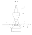
次に、図14に示すように、ボンディングステージ31とボンディングツール32とを備えたインナーリードボンダ30にリール25を装着し、ボンディングステージ31の上面に沿って絶縁フィルム2を移動させながら、アンテナ3に半導体チップ5を接続する。
【0038】
アンテナ3に半導体チップ5を接続するには、図15(図14の要部拡大図)に示すように、100℃程度に加熱したボンディングステージ31の上に半導体チップ5を搭載し、この半導体チップ5の真上に絶縁フィルム2のデバイスホール8を位置決めした後、デバイスホール8の内側に突出したリード10の上面に400℃程度に加熱したボンディングツール32を押し当て、Auバンプ(9a〜9d)とリード10を接触させる。このとき、ボンディングツール32に所定の荷重を2秒程度印加することにより、リード10の表面に形成されたSnメッキとAuバンプ(9a〜9d)との界面にAu−Sn共晶合金層が形成され、Auバンプ(9a〜9d)とリード10が互いに接着する。
【0039】
次に、ボンディングステージ31の上に新たな半導体チップ5を搭載し、続いて絶縁フィルム2をアンテナ3の1ピッチ分だけ移動させた後、上記と同様の操作を行うことによって、この半導体チップ5をアンテナ3に接続する。以後、上記と同様の操作を繰り返すことによって、絶縁フィルム2に形成された全てのアンテナ3に半導体チップ5を接続する。半導体チップ5とアンテナ3の接続作業が完了した絶縁フィルム2は、リール25に巻き取られた状態で次の樹脂封止工程に搬送される。
【0040】
なお、Auバンプ(9a〜9d)とリード10の接続信頼性を向上させるためには、図16に示すように、4本のリード10をアンテナ3の長辺方向と直交する方向に延在させた方がよい。図17に示すように、4本のリード10をアンテナ3の長辺方向と平行に延在させた場合は、完成したインレット1を折り曲げたときに、Auバンプ(9a〜9d)とリード10の接合部に強い引っ張り応力が働くので、両者の接続信頼性が低下する虞れがある。
【0041】
半導体チップ5の樹脂封止工程では、図18および図19に示すように、デバイスホール8の内側に実装された半導体チップ5の上面および側面にディスペンサ33などを使ってポッティング樹脂4を供給し、その後、ポッティング樹脂4を加熱炉内でベークする。図示は省略するが、この樹脂封止工程においても、絶縁フィルム2を移動させながら、ポッティング樹脂4の供給およびベーク処理を行う。そして、樹脂封止作業が完了した絶縁フィルム2は、リール25に巻き取られた状態で次の検査工程に搬送され、半導体チップ5とアンテナ3の接続状態や外観の良否の検査が行われる。絶縁フィルム2に形成された多数のアンテナ3は、互いに電気的に分離された状態になっているので、個々のアンテナ3と半導体チップ5の導通試験は、容易に実施することができる。その後、絶縁フィルム2の一面(アンテナ3が形成された面)にカバーフィルム6(図3参照)をラミネートすることにより、インレット1の製造工程が完了する。
【0042】
上記のようにして製造されたインレット1は、図20に示すように、リール25に巻き取られた状態で梱包され、顧客先に出荷される。
【0043】
上記インレット1を購入した顧客は、絶縁フィルム2を切断することによって、前記図1〜図5に示すような個片化されたインレット1を得た後、このインレット1と他の部材とを組み合わせて電子タグを作製する。例えば図21は、インレット1の裏面に両面接着テープなどを貼り付けて電子タグを作製し、これを伝票34などの物品の表面に貼り付けた例を示している。
【0044】
上記した本実施の形態によれば、フレキシブルな絶縁フィルム2の一面に貼り付けた薄いCu箔によってアンテナ3を構成しているので、Cuを基材とするアンテナを有するインレットに比較して、薄型であり、かつ柔軟性に富むインレット1を実現することができる。また、アンテナ3と一体に形成されたリード10に半導体チップ5の端子(Auバンプ9a、9b)を直接接続しているので、ボンディングワイヤを使ってアンテナ3と半導体チップ5を接続する方式に比べると、ワイヤのループがない分、インレット1の厚さを薄くすることができる。
また、多数のアンテナ3を所定の間隔で形成した絶縁フィルム2を使用することにより、インレット1の製造、すなわちアンテナ3と半導体チップ5の接続、半導体チップ5の樹脂封止および検査とその後の出荷を一貫して行うことができる。
【0045】
また、半導体チップ5を絶縁フィルムのデバイスホール8内に配置し、デバイスホール8の内側でリード10と半導体チップ5の端子を接続しているので、リード10と端子の接続部の外観検査が容易であると共に、ポッティング樹脂4の充填によるリード10と端子の接続部の保護も容易である。
【0046】
前記実施の形態では、デバイスホール8を形成した絶縁フィルム2を使用してインレット1を製造したが、例えば図22に示すように、デバイスホール8を有しない絶縁フィルム12の一面に前述した方法でアンテナ3およびリード10を一体形成し、このリード10に半導体チップ5の端子(Auバンプ9a、9b)を接続してもよい。この場合は、リード10と端子(Auバンプ9a、9b)を接続した後、図23に示すように、リード10と端子(Auバンプ9a、9b)の隙間にアンダーフィル樹脂13を充填する。
【0047】
上記のような絶縁フィルム12を使用する場合は、デバイスホール8を形成した絶縁フィルム2を使用する場合に比べてリード10と端子(Auバンプ9a、9b)の接続を確実に行うことができるので、両者の接続信頼性が向上し、ダミーバンプ(9c、9d)を省略することも可能である。但し、絶縁フィルム12の裏面側からリード10と端子(Auバンプ9a、9b)の接続部を視認できないので、外観検査方法に工夫が必要となる。また、リード10と端子(Auバンプ9a、9b)の極めて狭い隙間にアンダーフィル樹脂13を確実に充填するための工夫が必要となる。
【0048】
前記実施の形態では、ポリイミド樹脂からなる絶縁フィルム2に貼り付けたCu箔を使ってアンテナ3を構成したが、例えば絶縁フィルム2の一面に貼り付けたAl(アルミニウム)箔を使ってアンテナ3を構成したり、絶縁フィルム2をポリイミド樹脂よりも安価な樹脂(例えばポリエチレンテレフタレートなど)で構成したりすることにより、インレット1の材料コストを低減することができる。アンテナ3をAl箔で構成した場合、半導体チップ5のAuバンプ(9a〜9d)とアンテナ3との接続は、例えば超音波と加熱を併用したAu/Al接合の形成によって行うことが好ましい。
【0049】
(実施の形態2)
前記実施の形態1では、デバイスホール8を形成した絶縁フィルム2を使用してインレット1を製造したが、本実施の形態では、前記図22、図23に示したようなデバイスホールを有しない絶縁フィルム12を使ったCOF(Chip On Film)型インレットの製造方法の一例を説明する。
【0050】
図24は、COF型インレットの製造に用いる絶縁フィルム12の一部を示す平面図である。絶縁フィルム12は、例えば厚さ38μm程度の薄いポリイミド樹脂フィルムからなり、その一面には、スリット15を設けた多数のアンテナ14が所定の間隔で形成されている。アンテナ14は、Cuを主成分とする金属膜で構成される。
【0051】
上記アンテナ14を形成するには、まず絶縁フィルム12の表面にスパッタリング法で0.1μm以下の薄いCu膜を形成した後、このCu膜の表面に電解メッキ法で膜厚9μm程度のCu膜を成長させる。次に、フォトリソグラフィ技術を使ってこれらのCu膜をアンテナ14の形状にパターニングした後、その表面に無電解メッキ法で膜厚0.46μm程度のSn膜を形成する。
【0052】
上記のような方法でアンテナ14を形成した絶縁フィルム12は、Cu箔を接着してアンテナを形成した前記実施の形態1の絶縁フィルム2に比べると、アンテナ14を構成するCu膜の膜厚が薄く、しかも絶縁フィルム12の表面にCu膜を形成する際に接着剤を使用しないので、薄く、可撓性に富んでおり、折り曲げ強度が非常に高いという特長がある。
【0053】
図25は、上記アンテナ14の中央部付近を拡大して示す平面図である。アンテナ14のほぼ中央部には、その一端がアンテナ14の外縁に達する「L」字状のスリット15が設けられており、このスリット15のコーナー部には、アンテナ14を構成するCu膜を取り除いて絶縁フィルム12を露出させた矩形の切り欠き16が設けられている。また、この切り欠き16の内側には、アンテナ14と一体に構成され、先端がスリット15のコーナー部方向に延在する4本のリードパターン17が形成されている。これら4本のリードパターン17の面積は、互いに同一である。スリット15、切り欠き16およびリードパターン17は、前述したCu膜をアンテナ14の形状にパターニングする際に同時に形成される。
【0054】
上記のような絶縁フィルム12を使用したCOF型インレットの製造は、図26に示すようなフローに従って行われる。
【0055】
まず、Auバンプウエハをダイシングすることによって得た半導体チップ5と、上記のようなアンテナ14が形成された絶縁フィルム12とを用意する。半導体チップ5は、前記実施の形態1で用いたものと同じもの(図8〜図11参照)である。また、絶縁フィルム12は、前記実施の形態1と同様、リールに巻かれた状態で製造ラインに搬入される。
【0056】
次に、図27に示すように、ボンディングステージ31とボンディングツール32とを備えたインナーリードボンダ30にリール25を装着し、ボンディングステージ31の上面に沿って絶縁フィルム12を移動させながら、アンテナ14と半導体チップ5の接続(リードボンディング)を行う。
【0057】
具体的には、図28に示すように、450℃程度に加熱したボンディングステージ31の上に半導体チップ5を搭載し、この半導体チップ5の真上にアンテナ14のリードパターン17を位置決めした後、100℃程度に加熱したボンディングツール32を絶縁フィルム12の上面に押し当て、Auバンプ(9a〜9d)とリードパターン17とを接触させる。このとき、ボンディングツール32に所定の荷重を2秒程度印加することにより、リードパターン17の表面に形成されたSnメッキとAuバンプ(9a〜9d)との界面にAu−Sn共晶合金層が形成され、Auバンプ(9a〜9d)とリードパターン17とが接着する。
【0058】
図29は、半導体チップ5のAuバンプ(9a〜9d)とリードパターン17との重なり状態を示す平面図である。本実施の形態では、アンテナ14の一部に切り欠き16を形成し、この切り欠き16の内側に延在する4本のリードパターン17とAuバンプ(9a〜9d)とを接続するようにしたので、以下に述べる理由によって、アンテナ14と半導体チップ5との接続信頼性が高くなるという効果が得られる。
【0059】
すなわち、アンテナ14のスリット15のコーナー部に切り欠き16およびリードパターン17を形成しない場合は、例えば図30に示すように、スリット15を跨ぐアンテナ14の4箇所に半導体チップ5のAuバンプ(9a〜9d)を接続することになる。ところが、このようにした場合は、Auバンプ(9a〜9d)の位置によって、その周囲に形成されるCu膜のパターンが異なるため、熱拡散抵抗が異なる(図30に示す例では、Auバンプ9a、9cが接続される側の周囲の熱拡散経路は、Auバンプ9b、9dが接続される側の熱拡散経路よりも狭い)ため、ボンディングの際、熱拡散経路が広い側(Auバンプ9b、9dが接続される側)は、熱拡散経路が狭い側(Auバンプ9a、9cが接続される側)よりも熱の拡散経路における熱抵抗が小さく、熱の拡散量が多くなる。
【0060】
その結果、熱拡散経路が広い側でアンテナ14の表面温度が低下し、Auバンプ(9b、9d)とアンテナ14との界面でAu−Sn共晶合金層の形成が不十分となるために、Auバンプ(9b、9d)とアンテナ14との接着力が低下してしまう。また、例えば図31に示すような箇所でアンテナ14とAuバンプ(9a〜9d)とを接続した場合は熱拡散経路が広い側でアンテナ14と接する3個のAuバンプ(9b、9c、9d)は、熱拡散経路が狭い側でアンテナ14と接する1個のAuバンプ9aに比べてアンテナ14との接着強度が低下することになる。
【0061】
しかし、熱拡散経路が広い側でアンテナ14の表面温度が低下することを予め見越してボンディングステージ31やボンディングツール32の温度を高くすると、前記実施の形態1で用いた絶縁フィルム2のようなデバイスホール8を有しない絶縁フィルム12の場合は、チップ搭載領域の絶縁フィルム12が高温に曝されて熱変形し、不良品となってしまう。
【0062】
これに対し、チップ搭載領域のアンテナ14に前記のような切り欠き16およびリードパターン17を形成し、このリードパターン17とAuバンプ(9a〜9d)とを接続するようにした場合は、リードパターン17からの熱拡散経路が、切り欠きによって狭められているため、ボンディングの際にリードパターン17からアンテナ14へ向かう熱の拡散量が少なくなる。また、各リードパターンからの熱拡散経路が、切り欠きによってほぼ一様に狭められているため、4個のAuバンプ(9a〜9d)のそれぞれとリードパターン17との接合部は、ほぼ同じ温度になる。
【0063】
リードパターン17からアンテナ14へ向かう熱の拡散量は、リードパターン17の面積が小さいほど少なくなるが、小さすぎるとAuバンプ(9a〜9d)との接触面積も小さくなるので、両者の接合強度が低下する。従って、熱拡散量の抑制と接触面積の確保とを両立させるには、リードパターン17の幅をAuバンプ(9a〜9d)の直径よりも僅かに大きい寸法(Auバンプの直径+両者の合わせ余裕寸法)に設定すればよい。
【0064】
このように、チップ搭載領域のアンテナ14に切り欠き16およびリードパターン17を形成し、リードパターン17とAuバンプ(9a〜9d)とを接続することにより、ボンディングの際、Auバンプ(9a〜9d)とリードパターン17との接合部の温度低下を抑制することができると共に、4個のAuバンプ(9a〜9d)のそれぞれとリードパターン17との接合部の温度を均一にすることができる。これにより、Auバンプ(9a〜9d)とリードパターン17との界面に均一なAu−Sn共晶合金層が形成され、両者の接合強度を高めることができるので、アンテナ14と半導体チップ5との接続信頼性が高くなる。
【0065】
なお、チップ搭載領域のアンテナ14に設ける切り欠き16およびリードパターン17の形状は、上記したような鍬型ないしはスタグ(stag)型に限定されるものではなく、4個のAuバンプ(9a〜9d)と接触する部分の温度低下を防ぐと共に、温度均一性を実現することのできる形状であれば、任意の形状を採用することができる。
【0066】
次に、図32に示すように、半導体チップ5の下面と絶縁フィルム12(およびアンテナ14)との隙間にディスペンサ40などを使ってアンダーフィル樹脂41を充填した後、このアンダーフィル樹脂41を加熱炉内で硬化させる。アンダーフィル樹脂41を加熱炉内で硬化させる際は、まずアンダーフィル樹脂41を半硬化させて絶縁フィルム12をリール25に巻き取り、次に、このリール25を加熱炉内に搬入してアンダーフィル樹脂41を完全硬化する。また、アンダーフィル樹脂41を半硬化させた後、絶縁フィルム12をリール25に巻き取る工程に先立ち、アンテナ14と半導体チップ5との接続の良否を判定する検査を行ってもよい。
【0067】
図33に示すように、半導体チップ5の下面に充填するアンダーフィル樹脂41は、その最外縁部分が切り欠き16の外側のアンテナ14と接触していることが望ましい。すなわち、アンダーフィル樹脂41の径は、切り欠き16の径よりも大きいことが望ましい。これに対し、図34に示すように、アンダーフィル樹脂41の径が切り欠き16の径よりも小さい場合は、切り欠き16の内側の一部に、アンテナ14にもアンダーフィル樹脂41にも覆われていない絶縁フィルム12が露出する。
【0068】
絶縁フィルム12は、極めて膜厚が薄いため、完成したインレットの一部に膜厚が薄い部分が存在すると、インレットを折り曲げた際、この薄い部分に応力が加わり、半導体チップ5がアンテナ14から剥離する虞れがある。従って、前記図32に示したように、切り欠き16の内側の絶縁フィルム12は、アンダーフィル樹脂41で覆われていることが望ましい。またその際、図35に示すように、切り欠き16の径を半導体チップ5の径よりも小さくすることにより、切り欠き16の内側の絶縁フィルム12がアンダーフィル樹脂41と半導体チップ5で覆われることになるので、半導体チップ5とアンテナ14の接合部近傍のフィルム強度がさらに向上する。
【0069】
従って、アンテナ14に切り欠き16およびリードパターン17を形成する際には、アンダーフィル樹脂41や半導体チップ5の寸法を考慮した上で、それらの形状や寸法を設計することが望ましい。
【0070】
また、アンダーフィル樹脂41は、エポキシなどの有機系樹脂で構成されているので、半導体チップ5の最表面にポリイミド樹脂などの有機系樹脂を形成しておくとよい。これにより、アンダーフィル樹脂41と半導体チップ5との接着力が強化されるので、完成したインレットの折り曲げ強度(半導体チップ5とアンテナ14との接続強度)が向上する。
【0071】
上記した半導体チップ5の樹脂封止が完了すると、インレットの製造工程がほぼ終了する。このようにして製造されたCOF型インレットは、外観検査工程や最終選別工程を経た後、リールに巻き取られた状態で梱包されて顧客先に出荷され、絶縁フィルム12から切断、分離される。
【0072】
このように、本実施の形態によれば、薄く、小型で、しかも折り曲げ強度が非常に高いCOF型インレットを製造することができるので、熱、水分、機械的応力などが加わる劣悪な環境下での使用にも耐えられるインレットを提供することができる。
【0073】
以上、本発明者によってなされた発明を実施の形態に基づき具体的に説明したが、本発明は前記実施の形態に限定されるものではなく、その要旨を逸脱しない範囲で種々変更可能であることはいうまでもない。
【0074】
【発明の効果】
本願において開示される発明のうち、代表的なものによって得られる効果を簡単に説明すれば以下のとおりである。
【0075】
本発明の一態様によれば、薄型で曲げ強度が高い電子タグ用インレットを低価格で実現することができる。
【図面の簡単な説明】
【図1】本発明の一実施の形態である電子タグ用インレットを示す平面図(表面側)である。
【図2】図1の一部を拡大して示す平面図である。
【図3】本発明の一実施の形態である電子タグ用インレットを示す側面図である。
【図4】本発明の一実施の形態である電子タグ用インレットを示す平面図(裏面側)である。
【図5】図4の一部を拡大して示す平面図である。
【図6】本発明の一実施の形態である電子タグ用インレットの要部拡大平面図(表面側)である。
【図7】本発明の一実施の形態である電子タグ用インレットの要部拡大平面図(裏面側)である。
【図8】本発明の一実施の形態である電子タグ用インレットに実装された半導体チップの平面図である。
【図9】図8に示す半導体チップの主面に形成されたバンプ電極およびその近傍の断面図である。
【図10】図8に示す半導体チップの主面に形成されたダミーバンプ電極およびその近傍の断面図である。
【図11】図8に示す半導体チップの主面に形成された回路のブロック図である。
【図12】本発明の一実施の形態である電子タグ用インレットの製造に用いる長尺の絶縁フィルムの一部を示す平面図である。
【図13】図12に示す絶縁フィルムの一部を拡大して示す平面図である。
【図14】本発明の一実施の形態である電子タグ用インレットの製造工程の一部(半導体チップとアンテナの接続工程)を示すインナーリードボンダの概略図である。
【図15】図14に示すインナーリードボンダの要部を拡大して示す概略図である。
【図16】本発明の一実施の形態である電子タグ用インレットの製造工程の一部(半導体チップとアンテナの接続工程)を示す絶縁フィルムの要部拡大平面図である。
【図17】本発明の一実施の形態である電子タグ用インレットの製造工程の一部(半導体チップとアンテナの接続工程)を示す絶縁フィルムの要部拡大平面図である。
【図18】本発明の一実施の形態である電子タグ用インレットの製造工程の一部(半導体チップの樹脂封止工程)を示す概略図である。
【図19】本発明の一実施の形態である電子タグ用インレットの製造工程の一部(半導体チップの樹脂封止工程)を示す絶縁フィルムの要部拡大平面図である。
【図20】本発明の一実施の形態である電子タグ用インレットの製造に用いる絶縁フィルムをリールに巻き取った状態を示す側面図である。
【図21】本発明の一実施の形態である電子タグ用インレットを用いた電子タグの使用方法を示す説明図である。
【図22】本発明の他の実施の形態である電子タグ用インレットの製造工程の一部(半導体チップとアンテナの接続工程)を示す絶縁フィルムの要部拡大断面図である。
【図23】本発明の他の実施の形態である電子タグ用インレットの製造工程の一部(半導体チップとアンテナの接続工程)を示す絶縁フィルムの要部拡大断面図である。
【図24】本発明の他の実施の形態である電子タグ用インレットの製造に用いる長尺の絶縁フィルムの一部を示す平面図である。
【図25】図24に示す絶縁フィルムに形成されたアンテナの一部を拡大して示す平面図である。
【図26】本発明の他の実施の形態である電子タグ用インレットの製造工程を示すフロー図である。
【図27】本発明の他の実施の形態である電子タグ用インレットの製造工程の一部(半導体チップとアンテナの接続工程)を示すインナーリードボンダの概略図である。
【図28】図27に示すインナーリードボンダの要部を拡大して示す概略図である。
【図29】半導体チップのAuバンプとリードパターンとの重なり状態を示す平面図である。
【図30】半導体チップのAuバンプとリードパターンとの重なり状態の比較例を示す平面図である。
【図31】半導体チップのAuバンプとリードパターンとの重なり状態を比較例を示す平面図である。
【図32】本発明の他の実施の形態である電子タグ用インレットの製造工程の一部(半導体チップの樹脂封止工程)を示す概略図である。
【図33】アンテナの一部に形成された切り欠きの寸法と、半導体チップを封止する樹脂の寸法との関係の一例を示す平面図である。
【図34】アンテナの一部に形成された切り欠きの寸法と、半導体チップを封止する樹脂の寸法との関係の他の例を示す平面図である。
【図35】アンテナの一部に形成された切り欠きの寸法と、半導体チップの寸法と、半導体チップを封止する樹脂の寸法との関係の一例を示す平面図である。
【符号の説明】
1 電子タグ用インレット
2 絶縁フィルム
3 アンテナ
4 ポッティング樹脂
5 半導体チップ
6 カバーフィルム
7 スリット
8 デバイスホール
9a、9b Auバンプ
9c、9d ダミーバンプ
10 リード
12 絶縁フィルム
13 アンダーフィル樹脂
14 アンテナ
15 スリット
16 切り欠き
17 リードパターン
20 パッシベーション膜
21 ポリイミド樹脂
22 最上層メタル配線
23 バリアメタル膜
24 メタル層
25 リール
26 スプロケットホール
30 インナーリードボンダ
31 ボンディングステージ
32 ボンディングツール
33 ディスペンサ
34 伝票
40 ディスペンサ
41 アンダーフィル樹脂[0001]
BACKGROUND OF THE INVENTION
The present invention relates to an inlet for a non-contact type electronic tag, and more particularly, to a technology effective when applied to a thinner and highly reliable electronic tag inlet.
[0002]
[Prior art]
A non-contact type electronic tag is a tag in which desired data is stored in a memory circuit in a semiconductor chip and this data is read using a microwave.
[0003]
Japanese Patent Laid-Open No. 10-13296 (Patent Document 1) discloses an example of this type of non-contact type electronic tag. This electronic tag has a structure in which a microwave receiving antenna is constituted by a lead frame, and a semiconductor chip mounted on the lead frame is sealed with a resin.
[0004]
[Patent Document 1]
Japanese Patent Laid-Open No. 10-13296
[0005]
[Problems to be solved by the invention]
Since the electronic tag stores data in a memory circuit in the semiconductor chip, there is an advantage that a large amount of data can be stored as compared with a tag using a barcode. In addition, the data stored in the memory circuit has an advantage that unauthorized tampering is difficult as compared with the data stored in the barcode.
[0006]
However, since this type of electronic tag has a more complicated structure than a tag using a barcode or the like, its manufacturing cost is high, which is one factor hindering the spread of the electronic tag.
[0007]
Accordingly, the present inventor has been developing an inexpensive electronic tag inlet having a simplified structure. This inlet has a structure in which a semiconductor chip is mounted on an antenna constituted by a lead frame, the antenna and the semiconductor chip are electrically connected by an Au wire, and the semiconductor chip and the Au wire are sealed with a potting resin.
[0008]
However, since the inlet connects the antenna composed of the lead frame and the semiconductor chip with an Au wire, if the semiconductor chip and the Au wire are sealed with potting resin, the thickness of the entire inlet increases to about 0.6 mm. As a result, there arises a problem that the thinning required for the inlet for the electronic tag cannot be realized and a problem that it is difficult to obtain sufficient flexibility against bending deformation of the antenna portion.
[0009]
An object of the present invention is to provide a technique capable of realizing thinning and high reliability of an inlet for an electronic tag.
[0010]
Another object of the present invention is to provide a technique capable of realizing an electronic tag inlet that is thin, flexible, and inexpensive.
[0011]
The above and other objects and novel features of the present invention will be apparent from the description of this specification and the accompanying drawings.
[0012]
[Means for Solving the Problems]
Of the inventions disclosed in the present application, the outline of typical ones will be briefly described as follows.
[0013]
An inlet for an electronic tag of the present invention includes an insulating film, an antenna formed of a conductor layer formed on one surface of the insulating film, a slit formed on a part of the antenna, and one end extending to an outer edge of the antenna. And a semiconductor chip electrically connected to the antenna via a plurality of bump electrodes, and a resin for sealing the semiconductor chip.
[0014]
The inlet for an electronic tag of the present invention is provided with a notch in which the insulating film is exposed in a part of the antenna, one end is connected to the antenna inside the notch, and the other end is the notch. A plurality of lead patterns made of the conductive film extending inward are formed, and the plurality of bump electrodes are connected to the surface of the lead pattern formed at a corresponding position of each bump electrode. It is.
[0015]
The method for manufacturing an inlet for an electronic tag according to the present invention includes (a) a step of preparing an insulating film, (b) a step of forming a conductor film on one surface of the insulating film, and (c) a part of the conductor film. Forming a notch for exposing the insulating film to the semiconductor film, (d) electrically connecting the semiconductor chip to the conductor film via a plurality of bump electrodes, and (e) the semiconductor chip and the insulating film. A step of filling the gap with a resin, and in the step (c), one end is connected to the conductor film, the other end extends inside the notch, and a plurality of the conductor films Lead patterns are formed inside the notches, and in the step (d), the plurality of bump electrodes are electrically connected to the lead patterns, respectively, and in the step (d), a heated bonding stay is formed. The semiconductor chip is mounted thereon, and after positioning the plurality of lead patterns directly above the semiconductor chip, a heated bonding tool is pressed from the insulating film side, and the plurality of bump electrodes and the plurality of leads are pressed. Each pattern is electrically connected.
[0016]
DETAILED DESCRIPTION OF THE INVENTION
Hereinafter, embodiments of the present invention will be described in detail with reference to the drawings. Note that components having the same function are denoted by the same reference symbols throughout the drawings for describing the embodiment, and the repetitive description thereof will be omitted.
[0017]
(Embodiment 1)
FIG. 1 is a plan view (front side) showing an electronic tag inlet of this embodiment, FIG. 2 is a plan view showing a part of FIG. 1 in an enlarged manner, and FIG. 3 is an electronic tag inlet of this embodiment. FIG. 4 is a plan view (back side) showing the electronic tag inlet of the present embodiment, and FIG. 5 is an enlarged plan view showing a part of FIG.
[0018]
An electronic tag inlet (hereinafter simply referred to as an inlet) 1 of the present embodiment constitutes a main part of a non-contact type electronic tag provided with an antenna for receiving microwaves. This
[0019]
The length of the
[0020]
An “L” -
[0021]
6 and 7 are enlarged plan views showing the vicinity of the central portion of the
[0022]
As shown in the figure, a
[0023]
As shown in FIG. 6, on the main surface of the
[0024]
Of the four leads 10, two leads 10 extend from one of the
[0025]
FIG. 8 is a plan view showing a layout of four
[0026]
The
[0027]
Four Au bumps 9a, 9b, 9c and 9d are formed on the main surface of the
[0028]
The layout of these Au bumps 9a, 9b, 9c, and 9d is not limited to the layout shown in FIG. 8, but is preferably a layout that easily balances the weight at the time of chip connection. It is preferable that the polygon formed by the tangent line of the Au bump in the planar layout is arranged so as to surround the center of the chip.
[0029]
Of the four
[0030]
As shown in FIG. 9, the
[0031]
As described above, the
[0032]
In addition, the
[0033]
Next, the manufacturing method of the
[0034]
FIG. 12 is a plan view showing the insulating
[0035]
As shown in the drawing, the insulating
[0036]
The insulating
[0037]
Next, as shown in FIG. 14, the
[0038]
In order to connect the
[0039]
Next, a
[0040]
In order to improve the connection reliability between the Au bumps (9a to 9d) and the
[0041]
In the resin sealing process of the
[0042]
As shown in FIG. 20, the
[0043]
A customer who has purchased the
[0044]
According to the above-described embodiment, since the
Further, by using the insulating
[0045]
Further, since the
[0046]
In the embodiment, the
[0047]
When the insulating
[0048]
In the above-described embodiment, the
[0049]
(Embodiment 2)
In the first embodiment, the
[0050]
FIG. 24 is a plan view showing a part of the insulating
[0051]
In order to form the
[0052]
The insulating
[0053]
FIG. 25 is an enlarged plan view showing the vicinity of the central portion of the
[0054]
The manufacture of the COF type inlet using the insulating
[0055]
First, the
[0056]
Next, as shown in FIG. 27, the
[0057]
Specifically, as shown in FIG. 28, after mounting the
[0058]
FIG. 29 is a plan view showing an overlapping state between the Au bumps (9 a to 9 d) of the
[0059]
That is, when the
[0060]
As a result, the surface temperature of the
[0061]
However, when the temperature of the
[0062]
On the other hand, when the
[0063]
The amount of heat diffused from the
[0064]
In this way, the
[0065]
Note that the shape of the
[0066]
Next, as shown in FIG. 32, a gap between the lower surface of the
[0067]
As shown in FIG. 33, the
[0068]
Since the insulating
[0069]
Therefore, when forming the
[0070]
Further, since the
[0071]
When the above-described resin sealing of the
[0072]
As described above, according to the present embodiment, a COF inlet having a small thickness, a small size, and a very high bending strength can be manufactured. Therefore, in a poor environment to which heat, moisture, mechanical stress, and the like are applied. It is possible to provide an inlet that can withstand use.
[0073]
As mentioned above, the invention made by the present inventor has been specifically described based on the embodiment. However, the present invention is not limited to the embodiment, and various modifications can be made without departing from the scope of the invention. Needless to say.
[0074]
【The invention's effect】
Among the inventions disclosed in the present application, effects obtained by typical ones will be briefly described as follows.
[0075]
According to one embodiment of the present invention, an inlet for an electronic tag that is thin and has high bending strength can be realized at a low price.
[Brief description of the drawings]
FIG. 1 is a plan view (front side) showing an electronic tag inlet according to an embodiment of the present invention.
2 is an enlarged plan view showing a part of FIG. 1. FIG.
FIG. 3 is a side view showing an electronic tag inlet according to an embodiment of the present invention.
FIG. 4 is a plan view (back side) showing an electronic tag inlet according to an embodiment of the present invention.
5 is an enlarged plan view showing a part of FIG. 4; FIG.
FIG. 6 is an enlarged plan view (surface side) of a main part of an inlet for an electronic tag according to an embodiment of the present invention.
FIG. 7 is an enlarged plan view (back side) of a main part of an inlet for an electronic tag according to an embodiment of the present invention.
FIG. 8 is a plan view of a semiconductor chip mounted on an electronic tag inlet according to an embodiment of the present invention.
FIG. 9 is a cross-sectional view of a bump electrode formed on the main surface of the semiconductor chip shown in FIG. 8 and the vicinity thereof.
10 is a cross-sectional view of a dummy bump electrode formed on the main surface of the semiconductor chip shown in FIG. 8 and the vicinity thereof.
11 is a block diagram of a circuit formed on the main surface of the semiconductor chip shown in FIG. 8;
FIG. 12 is a plan view showing a part of a long insulating film used for manufacturing an inlet for an electronic tag according to an embodiment of the present invention.
13 is an enlarged plan view showing a part of the insulating film shown in FIG.
FIG. 14 is a schematic view of an inner lead bonder showing a part of the manufacturing process of the electronic tag inlet according to the embodiment of the present invention (a process of connecting the semiconductor chip and the antenna).
15 is an enlarged schematic view showing a main part of the inner lead bonder shown in FIG.
FIG. 16 is an enlarged plan view of an essential part of the insulating film showing a part of the manufacturing process of the electronic tag inlet according to the embodiment of the present invention (a process of connecting the semiconductor chip and the antenna).
FIG. 17 is an enlarged plan view of a main part of the insulating film showing a part of the manufacturing process of the electronic tag inlet according to the embodiment of the present invention (semiconductor chip and antenna connection process).
18 is a schematic view showing a part of a manufacturing process of an electronic tag inlet (semiconductor chip resin sealing process) according to an embodiment of the present invention; FIG.
FIG. 19 is an enlarged plan view of a main part of the insulating film showing a part of the manufacturing process of the electronic tag inlet according to the embodiment of the present invention (semiconductor chip resin sealing process);
FIG. 20 is a side view showing a state in which an insulating film used for manufacturing an inlet for an electronic tag according to an embodiment of the present invention is wound on a reel.
FIG. 21 is an explanatory diagram showing a method of using an electronic tag using an electronic tag inlet according to an embodiment of the present invention.
FIG. 22 is an enlarged cross-sectional view of a main part of an insulating film showing a part of a manufacturing process of an electronic tag inlet according to another embodiment of the present invention (a process of connecting a semiconductor chip and an antenna).
FIG. 23 is an enlarged cross-sectional view of the main part of the insulating film showing a part of the manufacturing process of the electronic tag inlet according to another embodiment of the present invention (semiconductor chip and antenna connection process).
FIG. 24 is a plan view showing a part of a long insulating film used for manufacturing an inlet for an electronic tag according to another embodiment of the present invention.
25 is an enlarged plan view showing a part of the antenna formed on the insulating film shown in FIG. 24. FIG.
FIG. 26 is a flowchart showing manufacturing steps of an electronic tag inlet according to another embodiment of the present invention.
FIG. 27 is a schematic view of an inner lead bonder showing a part of a manufacturing process of an electronic tag inlet according to another embodiment of the present invention (a process of connecting a semiconductor chip and an antenna).
28 is an enlarged schematic view showing a main part of the inner lead bonder shown in FIG. 27. FIG.
FIG. 29 is a plan view showing an overlapping state of Au bumps and lead patterns of a semiconductor chip.
30 is a plan view showing a comparative example of the overlapping state of Au bumps and lead patterns of a semiconductor chip. FIG.
FIG. 31 is a plan view showing a comparative example of the overlapping state of Au bumps and lead patterns of a semiconductor chip.
FIG. 32 is a schematic view showing a part of a manufacturing process of an electronic tag inlet according to another embodiment of the present invention (semiconductor chip resin sealing process);
FIG. 33 is a plan view showing an example of the relationship between the size of a notch formed in a part of an antenna and the size of a resin for sealing a semiconductor chip.
FIG. 34 is a plan view showing another example of the relationship between the size of the notch formed in a part of the antenna and the size of the resin for sealing the semiconductor chip.
FIG. 35 is a plan view showing an example of the relationship between the size of a notch formed in a part of an antenna, the size of a semiconductor chip, and the size of a resin that seals the semiconductor chip.
[Explanation of symbols]
1 Inlet for electronic tags
2 Insulating film
3 Antenna
4 Potting resin
5 Semiconductor chip
6 Cover film
7 Slit
8 Device hole
9a, 9b Au bump
9c, 9d Dummy bump
10 lead
12 Insulation film
13 Underfill resin
14 Antenna
15 slit
16 Notch
17 Lead pattern
20 Passivation film
21 Polyimide resin
22 Top layer metal wiring
23 Barrier metal film
24 Metal layer
25 reel
26 Sprocket hole
30 Inner lead bonder
31 Bonding stage
32 Bonding tools
33 Dispenser
34 slips
40 dispensers
41 Underfill resin
Claims (8)
(b)前記絶縁フィルムの一面上に導体膜を形成する工程と、(B) forming a conductor film on one surface of the insulating film;
(c)前記導体膜の一部に前記絶縁フィルムを露出させる切り欠きを形成する工程と、(C) forming a notch that exposes the insulating film in a part of the conductor film;
(d)複数のバンプ電極を介して前記導体膜に半導体チップを電気的に接続する工程と、(D) electrically connecting a semiconductor chip to the conductor film via a plurality of bump electrodes;
(e)前記半導体チップと前記絶縁フィルムとの隙間に樹脂を充填する工程とを有し、(E) having a step of filling a resin in a gap between the semiconductor chip and the insulating film;
前記(c)工程では、一端が前記導体膜に接続され、他端が前記切り欠きの内側に延在し、かつ前記導体膜からなる複数のリードパターンが前記切り欠きの内側に形成され、In the step (c), one end is connected to the conductor film, the other end extends to the inside of the notch, and a plurality of lead patterns made of the conductor film are formed inside the notch,
前記(d)工程では、前記複数のバンプ電極が前記複数のリードパターンにそれぞれ電気的に接続され、In the step (d), the plurality of bump electrodes are electrically connected to the plurality of lead patterns,
前記(d)工程では、加熱したボンディングステージ上に前記半導体チップを搭載し、前記半導体チップの真上に前記複数のリードパターンを位置決めした後、加熱したボンディングツールを前記絶縁フィルム側から押し当てて、前記複数のバンプ電極と前記複数のリードパターンをそれぞれ電気的に接続することを特徴とする電子タグ用インレットの製造方法。In the step (d), the semiconductor chip is mounted on a heated bonding stage, the lead patterns are positioned right above the semiconductor chip, and then the heated bonding tool is pressed from the insulating film side. The method of manufacturing an inlet for an electronic tag, wherein the plurality of bump electrodes and the plurality of lead patterns are electrically connected to each other.
前記(b)工程では、前記導体膜を前記絶縁フィルムの前記第1主面上に形成し、In the step (b), the conductor film is formed on the first main surface of the insulating film,
前記(d)工程では、前記ボンディングツールを前記絶縁フィルムの前記第2主面に押し当て、In the step (d), the bonding tool is pressed against the second main surface of the insulating film,
前記(e)工程では、前記樹脂を前記半導体チップと前記絶縁フィルムの前記第1主面との隙間に充填することを特徴とする請求項1記載の電子タグ用インレットの製造方法。The method for manufacturing an inlet for an electronic tag according to claim 1, wherein in the step (e), the resin is filled in a gap between the semiconductor chip and the first main surface of the insulating film.
Priority Applications (1)
| Application Number | Priority Date | Filing Date | Title |
|---|---|---|---|
| JP2003154302A JP4322558B2 (en) | 2003-05-30 | 2003-05-30 | Method for manufacturing inlet for electronic tag |
Applications Claiming Priority (1)
| Application Number | Priority Date | Filing Date | Title |
|---|---|---|---|
| JP2003154302A JP4322558B2 (en) | 2003-05-30 | 2003-05-30 | Method for manufacturing inlet for electronic tag |
Publications (3)
| Publication Number | Publication Date |
|---|---|
| JP2004355469A JP2004355469A (en) | 2004-12-16 |
| JP2004355469A5 JP2004355469A5 (en) | 2006-07-20 |
| JP4322558B2 true JP4322558B2 (en) | 2009-09-02 |
Family
ID=34048999
Family Applications (1)
| Application Number | Title | Priority Date | Filing Date |
|---|---|---|---|
| JP2003154302A Expired - Fee Related JP4322558B2 (en) | 2003-05-30 | 2003-05-30 | Method for manufacturing inlet for electronic tag |
Country Status (1)
| Country | Link |
|---|---|
| JP (1) | JP4322558B2 (en) |
Families Citing this family (13)
| Publication number | Priority date | Publication date | Assignee | Title |
|---|---|---|---|---|
| JP4712373B2 (en) * | 2004-12-27 | 2011-06-29 | ルネサスエレクトロニクス株式会社 | Manufacturing method of electronic tag inlet and electronic tag inlet |
| JP2006252050A (en) * | 2005-03-09 | 2006-09-21 | Matsushita Electric Ind Co Ltd | IC card module |
| JP2006347609A (en) | 2005-06-17 | 2006-12-28 | Renesas Technology Corp | Manufacturing method of carrier for conveying electronic parts |
| JP4815891B2 (en) * | 2005-06-22 | 2011-11-16 | 株式会社日立製作所 | Wireless IC tag and antenna manufacturing method |
| EP1770610A3 (en) * | 2005-09-29 | 2010-12-08 | Semiconductor Energy Laboratory Co., Ltd. | Semiconductor device |
| JP5004537B2 (en) * | 2005-09-29 | 2012-08-22 | 株式会社半導体エネルギー研究所 | Semiconductor device |
| JP4813160B2 (en) * | 2005-11-25 | 2011-11-09 | パナソニック株式会社 | IC module and non-contact IC card |
| JP4972983B2 (en) * | 2006-04-20 | 2012-07-11 | 大日本印刷株式会社 | IC chip mounting inspection method of non-contact IC tag and non-contact IC tag |
| JP2008066363A (en) * | 2006-09-05 | 2008-03-21 | Nec Tokin Corp | Non-contact IC medium and manufacturing method thereof |
| JP5000309B2 (en) * | 2007-01-10 | 2012-08-15 | 京セラケミカル株式会社 | Electronic component mounting method and electronic component module manufacturing method |
| JP5234071B2 (en) | 2010-09-03 | 2013-07-10 | 株式会社村田製作所 | RFIC module |
| JP6546739B2 (en) * | 2014-11-14 | 2019-07-17 | ローム株式会社 | Semiconductor integrated circuit device, method of manufacturing the same, and electronic device |
| JP7451237B2 (en) * | 2020-03-09 | 2024-03-18 | サトーホールディングス株式会社 | RFID inlay |
-
2003
- 2003-05-30 JP JP2003154302A patent/JP4322558B2/en not_active Expired - Fee Related
Also Published As
| Publication number | Publication date |
|---|---|
| JP2004355469A (en) | 2004-12-16 |
Similar Documents
| Publication | Publication Date | Title |
|---|---|---|
| JP4109039B2 (en) | Inlet for electronic tag and manufacturing method thereof | |
| US6593648B2 (en) | Semiconductor device and method of making the same, circuit board and electronic equipment | |
| US4974057A (en) | Semiconductor device package with circuit board and resin | |
| EP0498446B1 (en) | Multichip packaged semiconductor device and method for manufacturing the same | |
| JP2792532B2 (en) | Semiconductor device manufacturing method and semiconductor wafer | |
| US8999759B2 (en) | Method for fabricating packaging structure having embedded semiconductor element | |
| KR100396925B1 (en) | Flexible wiring substrate, film carrier, tapelike semiconductor device, semiconductor device, method of manufacture of semiconductor device, circuit board, and electronic device | |
| US6646335B2 (en) | Flexible tape carrier with external terminals formed on interposers | |
| TW469614B (en) | Semiconductor device and the manufacturing method for the same and electronic machine | |
| US8141786B2 (en) | Thin smart card module having strap on carrier | |
| JP4322558B2 (en) | Method for manufacturing inlet for electronic tag | |
| TW200411892A (en) | Semiconductor device and laminated semiconductor device | |
| US6744120B1 (en) | Flexible interconnect substrate of a tape-shaped semiconductor device, semiconductor device and circuit board | |
| US7176058B2 (en) | Chip scale package and method of fabricating the same | |
| US7396763B2 (en) | Semiconductor package using flexible film and method of manufacturing the same | |
| JPH0797594B2 (en) | Semiconductor integrated circuit device | |
| JP2008140400A (en) | Electronic tag and its manufacturing method | |
| JP2001332580A (en) | Semiconductor device and manufacturing method thereof | |
| US20100320598A1 (en) | Semiconductor device and fabrication method thereof | |
| KR19980079528A (en) | Semiconductor device and manufacturing method thereof | |
| JPH09270435A (en) | Method for manufacturing semiconductor device | |
| JP2000332143A (en) | Semiconductor device | |
| KR20250014840A (en) | Circuit board and semiconductor package comprising the same | |
| JP2001094031A (en) | Radio wave frequency tag and method for manufacturing it | |
| JPH0897359A (en) | Semiconductor device and method of manufacturing semiconductor device |
Legal Events
| Date | Code | Title | Description |
|---|---|---|---|
| A521 | Request for written amendment filed |
Free format text: JAPANESE INTERMEDIATE CODE: A523 Effective date: 20060529 |
|
| A621 | Written request for application examination |
Free format text: JAPANESE INTERMEDIATE CODE: A621 Effective date: 20060529 |
|
| A977 | Report on retrieval |
Free format text: JAPANESE INTERMEDIATE CODE: A971007 Effective date: 20090423 |
|
| TRDD | Decision of grant or rejection written | ||
| A01 | Written decision to grant a patent or to grant a registration (utility model) |
Free format text: JAPANESE INTERMEDIATE CODE: A01 Effective date: 20090507 |
|
| A01 | Written decision to grant a patent or to grant a registration (utility model) |
Free format text: JAPANESE INTERMEDIATE CODE: A01 |
|
| A61 | First payment of annual fees (during grant procedure) |
Free format text: JAPANESE INTERMEDIATE CODE: A61 Effective date: 20090603 |
|
| R150 | Certificate of patent or registration of utility model |
Free format text: JAPANESE INTERMEDIATE CODE: R150 |
|
| FPAY | Renewal fee payment (event date is renewal date of database) |
Free format text: PAYMENT UNTIL: 20120612 Year of fee payment: 3 |
|
| FPAY | Renewal fee payment (event date is renewal date of database) |
Free format text: PAYMENT UNTIL: 20120612 Year of fee payment: 3 |
|
| S111 | Request for change of ownership or part of ownership |
Free format text: JAPANESE INTERMEDIATE CODE: R313111 |
|
| FPAY | Renewal fee payment (event date is renewal date of database) |
Free format text: PAYMENT UNTIL: 20120612 Year of fee payment: 3 |
|
| R350 | Written notification of registration of transfer |
Free format text: JAPANESE INTERMEDIATE CODE: R350 |
|
| FPAY | Renewal fee payment (event date is renewal date of database) |
Free format text: PAYMENT UNTIL: 20120612 Year of fee payment: 3 |
|
| FPAY | Renewal fee payment (event date is renewal date of database) |
Free format text: PAYMENT UNTIL: 20130612 Year of fee payment: 4 |
|
| FPAY | Renewal fee payment (event date is renewal date of database) |
Free format text: PAYMENT UNTIL: 20130612 Year of fee payment: 4 |
|
| FPAY | Renewal fee payment (event date is renewal date of database) |
Free format text: PAYMENT UNTIL: 20140612 Year of fee payment: 5 |
|
| S531 | Written request for registration of change of domicile |
Free format text: JAPANESE INTERMEDIATE CODE: R313531 |
|
| R350 | Written notification of registration of transfer |
Free format text: JAPANESE INTERMEDIATE CODE: R350 |
|
| LAPS | Cancellation because of no payment of annual fees |