JP4257357B2 - Manufacturing method of semiconductor device - Google Patents
Manufacturing method of semiconductor device Download PDFInfo
- Publication number
- JP4257357B2 JP4257357B2 JP2006261823A JP2006261823A JP4257357B2 JP 4257357 B2 JP4257357 B2 JP 4257357B2 JP 2006261823 A JP2006261823 A JP 2006261823A JP 2006261823 A JP2006261823 A JP 2006261823A JP 4257357 B2 JP4257357 B2 JP 4257357B2
- Authority
- JP
- Japan
- Prior art keywords
- contact
- etching
- insulating film
- opening
- semiconductor device
- Prior art date
- Legal status (The legal status is an assumption and is not a legal conclusion. Google has not performed a legal analysis and makes no representation as to the accuracy of the status listed.)
- Expired - Fee Related
Links
- 239000004065 semiconductor Substances 0.000 title claims description 37
- 238000004519 manufacturing process Methods 0.000 title claims description 13
- 238000005530 etching Methods 0.000 claims description 79
- 238000000034 method Methods 0.000 claims description 47
- 230000008021 deposition Effects 0.000 claims description 35
- 239000000758 substrate Substances 0.000 claims description 11
- 230000000149 penetrating effect Effects 0.000 claims description 5
- 238000000151 deposition Methods 0.000 description 33
- 239000011229 interlayer Substances 0.000 description 20
- 238000001459 lithography Methods 0.000 description 20
- 239000007789 gas Substances 0.000 description 18
- 239000010410 layer Substances 0.000 description 15
- 229910052581 Si3N4 Inorganic materials 0.000 description 11
- HQVNEWCFYHHQES-UHFFFAOYSA-N silicon nitride Chemical compound N12[Si]34N5[Si]62N3[Si]51N64 HQVNEWCFYHHQES-UHFFFAOYSA-N 0.000 description 11
- 238000010586 diagram Methods 0.000 description 10
- XUIMIQQOPSSXEZ-UHFFFAOYSA-N Silicon Chemical compound [Si] XUIMIQQOPSSXEZ-UHFFFAOYSA-N 0.000 description 6
- 230000015572 biosynthetic process Effects 0.000 description 6
- 238000001312 dry etching Methods 0.000 description 6
- 229910052710 silicon Inorganic materials 0.000 description 6
- 239000010703 silicon Substances 0.000 description 6
- VYPSYNLAJGMNEJ-UHFFFAOYSA-N Silicium dioxide Chemical compound O=[Si]=O VYPSYNLAJGMNEJ-UHFFFAOYSA-N 0.000 description 4
- 238000002955 isolation Methods 0.000 description 4
- 229910052814 silicon oxide Inorganic materials 0.000 description 4
- 230000002093 peripheral effect Effects 0.000 description 3
- OKTJSMMVPCPJKN-UHFFFAOYSA-N Carbon Chemical compound [C] OKTJSMMVPCPJKN-UHFFFAOYSA-N 0.000 description 2
- QVGXLLKOCUKJST-UHFFFAOYSA-N atomic oxygen Chemical compound [O] QVGXLLKOCUKJST-UHFFFAOYSA-N 0.000 description 2
- 239000005380 borophosphosilicate glass Substances 0.000 description 2
- 229910052799 carbon Inorganic materials 0.000 description 2
- 229910052760 oxygen Inorganic materials 0.000 description 2
- 239000001301 oxygen Substances 0.000 description 2
- 238000000059 patterning Methods 0.000 description 2
- 238000000206 photolithography Methods 0.000 description 2
- 238000001020 plasma etching Methods 0.000 description 2
- 238000004380 ashing Methods 0.000 description 1
- 238000002508 contact lithography Methods 0.000 description 1
- 238000009413 insulation Methods 0.000 description 1
- 238000005468 ion implantation Methods 0.000 description 1
- 238000004518 low pressure chemical vapour deposition Methods 0.000 description 1
- 229910052756 noble gas Inorganic materials 0.000 description 1
- 239000011368 organic material Substances 0.000 description 1
- 239000000126 substance Substances 0.000 description 1
Images


Classifications
-
- H—ELECTRICITY
- H01—ELECTRIC ELEMENTS
- H01L—SEMICONDUCTOR DEVICES NOT COVERED BY CLASS H10
- H01L21/00—Processes or apparatus adapted for the manufacture or treatment of semiconductor or solid state devices or of parts thereof
- H01L21/70—Manufacture or treatment of devices consisting of a plurality of solid state components formed in or on a common substrate or of parts thereof; Manufacture of integrated circuit devices or of parts thereof
- H01L21/71—Manufacture of specific parts of devices defined in group H01L21/70
- H01L21/768—Applying interconnections to be used for carrying current between separate components within a device comprising conductors and dielectrics
- H01L21/76801—Applying interconnections to be used for carrying current between separate components within a device comprising conductors and dielectrics characterised by the formation and the after-treatment of the dielectrics, e.g. smoothing
- H01L21/76802—Applying interconnections to be used for carrying current between separate components within a device comprising conductors and dielectrics characterised by the formation and the after-treatment of the dielectrics, e.g. smoothing by forming openings in dielectrics
- H01L21/76816—Aspects relating to the layout of the pattern or to the size of vias or trenches
-
- H—ELECTRICITY
- H01—ELECTRIC ELEMENTS
- H01L—SEMICONDUCTOR DEVICES NOT COVERED BY CLASS H10
- H01L21/00—Processes or apparatus adapted for the manufacture or treatment of semiconductor or solid state devices or of parts thereof
- H01L21/02—Manufacture or treatment of semiconductor devices or of parts thereof
- H01L21/04—Manufacture or treatment of semiconductor devices or of parts thereof the devices having potential barriers, e.g. a PN junction, depletion layer or carrier concentration layer
- H01L21/18—Manufacture or treatment of semiconductor devices or of parts thereof the devices having potential barriers, e.g. a PN junction, depletion layer or carrier concentration layer the devices having semiconductor bodies comprising elements of Group IV of the Periodic Table or AIIIBV compounds with or without impurities, e.g. doping materials
- H01L21/30—Treatment of semiconductor bodies using processes or apparatus not provided for in groups H01L21/20 - H01L21/26
- H01L21/31—Treatment of semiconductor bodies using processes or apparatus not provided for in groups H01L21/20 - H01L21/26 to form insulating layers thereon, e.g. for masking or by using photolithographic techniques; After treatment of these layers; Selection of materials for these layers
- H01L21/3105—After-treatment
- H01L21/311—Etching the insulating layers by chemical or physical means
- H01L21/31105—Etching inorganic layers
- H01L21/31111—Etching inorganic layers by chemical means
- H01L21/31116—Etching inorganic layers by chemical means by dry-etching
-
- H—ELECTRICITY
- H01—ELECTRIC ELEMENTS
- H01L—SEMICONDUCTOR DEVICES NOT COVERED BY CLASS H10
- H01L21/00—Processes or apparatus adapted for the manufacture or treatment of semiconductor or solid state devices or of parts thereof
- H01L21/02—Manufacture or treatment of semiconductor devices or of parts thereof
- H01L21/04—Manufacture or treatment of semiconductor devices or of parts thereof the devices having potential barriers, e.g. a PN junction, depletion layer or carrier concentration layer
- H01L21/18—Manufacture or treatment of semiconductor devices or of parts thereof the devices having potential barriers, e.g. a PN junction, depletion layer or carrier concentration layer the devices having semiconductor bodies comprising elements of Group IV of the Periodic Table or AIIIBV compounds with or without impurities, e.g. doping materials
- H01L21/30—Treatment of semiconductor bodies using processes or apparatus not provided for in groups H01L21/20 - H01L21/26
- H01L21/31—Treatment of semiconductor bodies using processes or apparatus not provided for in groups H01L21/20 - H01L21/26 to form insulating layers thereon, e.g. for masking or by using photolithographic techniques; After treatment of these layers; Selection of materials for these layers
- H01L21/3105—After-treatment
- H01L21/311—Etching the insulating layers by chemical or physical means
- H01L21/31127—Etching organic layers
- H01L21/31133—Etching organic layers by chemical means
- H01L21/31138—Etching organic layers by chemical means by dry-etching
-
- H—ELECTRICITY
- H01—ELECTRIC ELEMENTS
- H01L—SEMICONDUCTOR DEVICES NOT COVERED BY CLASS H10
- H01L21/00—Processes or apparatus adapted for the manufacture or treatment of semiconductor or solid state devices or of parts thereof
- H01L21/02—Manufacture or treatment of semiconductor devices or of parts thereof
- H01L21/04—Manufacture or treatment of semiconductor devices or of parts thereof the devices having potential barriers, e.g. a PN junction, depletion layer or carrier concentration layer
- H01L21/18—Manufacture or treatment of semiconductor devices or of parts thereof the devices having potential barriers, e.g. a PN junction, depletion layer or carrier concentration layer the devices having semiconductor bodies comprising elements of Group IV of the Periodic Table or AIIIBV compounds with or without impurities, e.g. doping materials
- H01L21/30—Treatment of semiconductor bodies using processes or apparatus not provided for in groups H01L21/20 - H01L21/26
- H01L21/31—Treatment of semiconductor bodies using processes or apparatus not provided for in groups H01L21/20 - H01L21/26 to form insulating layers thereon, e.g. for masking or by using photolithographic techniques; After treatment of these layers; Selection of materials for these layers
- H01L21/3105—After-treatment
- H01L21/311—Etching the insulating layers by chemical or physical means
- H01L21/31144—Etching the insulating layers by chemical or physical means using masks
-
- H—ELECTRICITY
- H10—SEMICONDUCTOR DEVICES; ELECTRIC SOLID-STATE DEVICES NOT OTHERWISE PROVIDED FOR
- H10B—ELECTRONIC MEMORY DEVICES
- H10B12/00—Dynamic random access memory [DRAM] devices
- H10B12/01—Manufacture or treatment
- H10B12/09—Manufacture or treatment with simultaneous manufacture of the peripheral circuit region and memory cells
-
- H—ELECTRICITY
- H10—SEMICONDUCTOR DEVICES; ELECTRIC SOLID-STATE DEVICES NOT OTHERWISE PROVIDED FOR
- H10B—ELECTRONIC MEMORY DEVICES
- H10B12/00—Dynamic random access memory [DRAM] devices
- H10B12/30—DRAM devices comprising one-transistor - one-capacitor [1T-1C] memory cells
- H10B12/48—Data lines or contacts therefor
- H10B12/485—Bit line contacts
Landscapes
- Engineering & Computer Science (AREA)
- Manufacturing & Machinery (AREA)
- Computer Hardware Design (AREA)
- Physics & Mathematics (AREA)
- Condensed Matter Physics & Semiconductors (AREA)
- General Physics & Mathematics (AREA)
- Microelectronics & Electronic Packaging (AREA)
- Power Engineering (AREA)
- Chemical & Material Sciences (AREA)
- General Chemical & Material Sciences (AREA)
- Chemical Kinetics & Catalysis (AREA)
- Inorganic Chemistry (AREA)
- Internal Circuitry In Semiconductor Integrated Circuit Devices (AREA)
- Electrodes Of Semiconductors (AREA)
- Drying Of Semiconductors (AREA)
Description
本発明は、半導体プロセスに関する。 The present invention relates to a semiconductor process.
DRAMなどの半導体装置において、導電膜からなる下層プラグに、配線の間を通るコンタクトが開口されることがある。こうしたコンタクトは、次のような工程によって形成される。 In a semiconductor device such as a DRAM, a contact passing between wirings may be opened in a lower plug made of a conductive film. Such a contact is formed by the following process.
シリコン窒化膜をマスクとして配線が加工される。配線の側壁がシリコン窒化膜によって覆われる。その結果、配線の上部と側壁がシリコン窒化膜によって覆われる。配線層が絶縁膜で埋め込まれ、平坦化が行われる。リソグラフィ技術によりレジストパターニングされる。シリコン窒化膜と絶縁膜とのエッチング選択比が大きいドライエッチングによってコンタクトが加工される。 Wiring is processed using the silicon nitride film as a mask. The side walls of the wiring are covered with a silicon nitride film. As a result, the upper and side walls of the wiring are covered with the silicon nitride film. The wiring layer is filled with an insulating film, and planarization is performed. Resist patterning is performed by a lithography technique. The contact is processed by dry etching having a high etching selectivity between the silicon nitride film and the insulating film.
この方法は、SAC(Self Aligned Contact)と呼ばれ、一般的に用いられている。ところが近年、半導体のパターンの微細化に伴い、コンタクト加工時に絶縁膜とシリコン窒化膜とのエッチング選択比が大きい条件を満たすことが困難となってきている。このためSACという手法を使用することが困難になってきている。 This method is called SAC (Self Aligned Contact) and is generally used. However, in recent years, with the miniaturization of semiconductor patterns, it has become difficult to satisfy the condition that the etching selection ratio between the insulating film and the silicon nitride film is large during contact processing. For this reason, it has become difficult to use a technique called SAC.
SAC手法を使用せずにコンタクトを形成する場合、コンタクトを確実に配線に接触しないように形成する技術が求められる。そのような技術として、本発明の発明者は、径の小さいコンタクトを形成する技術に着目した。 When forming a contact without using the SAC technique, a technique for forming the contact so as not to contact the wiring is required. As such a technique, the inventors of the present invention focused on a technique for forming a contact having a small diameter.
配線の間に配置されるコンタクトの径をより小さく設定することにより、配線に接触しないようにコンタクトを形成する工程での位置決めの余裕幅がより大きく得られる。そのためにコンタクトの径は、製造工程で発生する可能性のあるズレを考慮してもコンタクトと配線とが接触しないように設定される。製造工程で発生する可能性のあるズレとして、コンタクトリソグラフィ工程での配線層に対する位置合わせマージン、コンタクト開口におけるコンタクトの寸法のばらつき、および配線層でのコンタクトの寸法ばらつきが挙げられる。例えば配線ピッチ190nm、配線間スペース140nmの場合、コンタクトの径は100nm以下に設定されることが望ましい。 By setting the diameter of the contacts arranged between the wirings to be smaller, a positioning margin in the process of forming the contacts so as not to contact the wirings can be obtained. Therefore, the diameter of the contact is set so that the contact and the wiring do not come into contact with each other even when a deviation that may occur in the manufacturing process is taken into consideration. Misalignment that may occur in the manufacturing process includes an alignment margin with respect to the wiring layer in the contact lithography process, a variation in contact dimensions in the contact opening, and a variation in contact dimensions in the wiring layer. For example, when the wiring pitch is 190 nm and the inter-wiring space is 140 nm, the contact diameter is preferably set to 100 nm or less.
一方、このような微小なコンタクトを製造する工程の後で、重ね合わせとアラインメントを行ってリソグラフィ工程が実施されることがある。そのため、微小なコンタクトを有する半導体装置には、アラインメントのために幅1μm以上の大面積トレンチが形成される。 On the other hand, after such a process for manufacturing a minute contact, a lithography process may be performed by performing overlay and alignment. Therefore, a large area trench having a width of 1 μm or more is formed in a semiconductor device having a minute contact for alignment.
すなわち、SAC手法を用いずに径の小さいコンタクトを形成する技術においては、極端に面積の異なるパターン(径100nm以下のコンタクトと、幅1μm以上のトレンチ)を同一の半導体装置に形成することが求められる。 That is, in a technique for forming a contact having a small diameter without using the SAC technique, it is required to form patterns (contacts having a diameter of 100 nm or less and trenches having a width of 1 μm or more) having extremely different areas in the same semiconductor device. It is done.
面積の異なるパターンを形成する技術の例として、特許文献1には、径の異なるコンタクトを開口する方法について記載されている。この方法によれば、自己整合コンタクト孔と共に、自己整合コンタクト孔よりも径の大きなコンタクト孔が形成される。以下、図1A〜1Dを参照して、この方法について説明する。
As an example of a technique for forming patterns having different areas,
図1Aに示される断面構造を備えた半導体装置が以下の工程により製造される。p型シリコン基板101上に設けられたメモリセル部のゲート電極105Gと、周辺回路部の第1の配線層105aが、SiN膜107で覆われる。ゲート電極105Gと第1の配線層105aは、BPSG膜109に覆われる。
A semiconductor device having the cross-sectional structure shown in FIG. 1A is manufactured by the following process. The
図1Bを参照して、パターニングされたレジストマスクにより、BPSG膜が選択的にエッチングされる。セルフアラインドコンタクト(SAC)による基板へのコンタクトホール111aがゲート電極間に、第1の配線層へのコンタクトホール111bが周辺回路部に形成される。コンタクトホール111aのホール径が0.15μm程度である場合、コンタクトホール111bのホール径は0.45μm程度であることが好ましいと記載されている。
Referring to FIG. 1B, the BPSG film is selectively etched by the patterned resist mask. A
図1Cを参照して、減圧CVD法によりドープトシリコン層が形成される。この形成によって、ドープトシリコン層は狭いコンタクトホール111aは埋め込むが、第1の配線層への広いコンタクトホール111bは埋め込まない。次いで、異方性エッチングにより平坦部上のドープトシリコン層が除去される。基板へのコンタクトホール111aにはプラグ113が形成される。第1の配線層へのコンタクトホール111bにはサイドウォール115が形成される。
Referring to FIG. 1C, a doped silicon layer is formed by a low pressure CVD method. By this formation, the
図1Dを参照して、第1の配線層105aの上のSiN膜7がドライエッチングされ、第1の配線層に達するコンタクトホール111cが自己整合的に形成される。
Referring to FIG. 1D, the SiN
この技術によれば、SACによる微細化において、周辺回路部の第1の配線層に接続するコンタクトホールを形成するために、さらなる工程が必要とされない。 According to this technique, in the miniaturization by SAC, no additional process is required to form the contact hole connected to the first wiring layer of the peripheral circuit portion.
この特許文献1に記載の技術においては、径の異なるコンタクトが加工されている。上記の例では、コンタクトの径は0.15μmと0.45μmである([0057])。これは、本発明が課題とする、径が100nm以下のコンタクトと幅1μm以上のトレンチに例示される極端にエッチング面積の異なるコンタクトを加工することとは異なる技術である。
In the technique described in
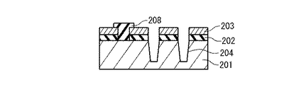
特許文献2には、アラインメントマークを形成する技術が記載されている。この技術について、図2Aから2Fを参照して説明する。 Patent Document 2 describes a technique for forming alignment marks. This technique will be described with reference to FIGS. 2A to 2F.
図2Aを参照して、シリコン基板201表面に窒化シリコン膜202が形成され、この上層にフォトリソグラフィによりレジストパターン203が形成されパターニングされる。
Referring to FIG. 2A, a
図2Bを参照して、レジストパターン203をマスクとしてエッチングが行われ、トレンチ形成領域に開口Hを有する窒化シリコン膜からなる第1のマスク202が形成される。
Referring to FIG. 2B, etching is performed using
図2Cを参照して、窒化シリコン膜が形成される。これがフォトリソグラフィによりパターニングされる。開口Hのうちアラインメントマーク形成領域の開口周縁を覆うように第3のマスク208が形成される。このマスク202を介してプラズマエッチングが行われ、素子分離のためのトレンチ204が形成される。
Referring to FIG. 2C, a silicon nitride film is formed. This is patterned by photolithography. A
図2Dを参照して、第3のマスク208が剥離除去される。CVD法により酸化シリコン膜が形成され、トレンチ204内部に酸化シリコン膜205が形成される。このとき第3のマスク208が除去されたあとのアラインメントマーク形成領域にも酸化シリコン膜が形成される。続いて、酸化シリコン膜205が除去されアラインメントマーク形成領域の基板表面201が露呈するまでCMPが行われる。
Referring to FIG. 2D, the
図2Eを参照して、シリコンのエッチングが行われ、アラインメントマーク形成領域にアラインメントマーク用トレンチ207が形成される。
Referring to FIG. 2E, silicon is etched to form an
図2Fを参照して、窒化シリコン膜202が除去され、表面の平坦な素子分離ウェハが形成される。
配線と接触しないようにコンタクトを形成するためには、コンタクトを開口するためのエッチングの工程において、リソグラフィパターンからの径の拡大が抑制されることが望まれる。すなわち、エッチングがリソグラフィパターンに対応して垂直に進み、リソグラフィパターンに水平な方向のエッチングが抑制されることが望まれる。 In order to form a contact so as not to come into contact with the wiring, it is desired that an increase in diameter from the lithography pattern is suppressed in an etching process for opening the contact. That is, it is desired that the etching proceeds vertically corresponding to the lithography pattern and that the etching in the direction horizontal to the lithography pattern is suppressed.
100nm以下の径の小さなコンタクトを、リソグラフィパターンからの径の拡大を抑制して開口するために、以下の条件でドライエッチングが行われる。条件1:対レジストマスク選択比が高い条件。条件2:デポジション種が多い条件。望ましくは、この両方の条件が設定される。 In order to open a contact having a small diameter of 100 nm or less while suppressing the expansion of the diameter from the lithography pattern, dry etching is performed under the following conditions. Condition 1: Conditions with a high resist mask selection ratio. Condition 2: Conditions with many deposition types. Desirably, both conditions are set.
ところが、このような条件下ではエッチング面積の広いトレンチ部分ではデポジション種がエッチング種よりも多くなり、エッチングがストップしてしまう。このようにエッチング面積の小さい部分に対してエッチング面積の大きい部分のエッチングレートが遅くなる現象は、逆マイクロローディング現象と呼ばれる。 However, under such conditions, the number of deposition species becomes larger than the etching species in the trench portion having a large etching area, and the etching stops. Such a phenomenon that the etching rate of the portion having a large etching area becomes slower than the portion having a small etching area is called a reverse microloading phenomenon.
この現象のために、通常のリソグラフィ工程によって100nm以下の径の小さなコンタクトと幅1μm以上のトレンチとを同一の半導体デバイス上に形成するためには、各々の開口を形成するためのリソグラフィ工程を別個に実施することが必要とされる。その結果としてリソグラフィ工程が増加するため、生産性を向上させることが困難となる。径の小さなコンタクトと大面積トレンチを少ない工程で形成する技術が望まれる。 Because of this phenomenon, in order to form a contact with a diameter of 100 nm or less and a trench with a width of 1 μm or more on the same semiconductor device by a normal lithography process, the lithography process for forming each opening is separately performed. Need to be implemented. As a result, the number of lithography processes increases, making it difficult to improve productivity. A technique for forming a contact with a small diameter and a large-area trench by a small number of processes is desired.
以下に、[発明を実施するための最良の形態]で使用される番号を括弧付きで用いて、課題を解決するための手段を説明する。これらの番号は、[特許請求の範囲]の記載と[発明を実施するための最良の形態]との対応関係を明らかにするために付加されたものである。ただし、それらの番号を、[特許請求の範囲]に記載されている発明の技術的範囲の解釈に用いてはならない。 In the following, means for solving the problem will be described using the numbers used in [Best Mode for Carrying Out the Invention] in parentheses. These numbers are added to clarify the correspondence between the description of [Claims] and [Best Mode for Carrying Out the Invention]. However, these numbers should not be used to interpret the technical scope of the invention described in [Claims].
本発明による半導体装置の製造方法は、半導体基板上に形成された積層構造中の絶縁膜(10)に開口幅の小さい第1開口部(13)と開口幅の大きい第2開口部(14)とを有するレジストマスク(12)を形成するステップと、第1開口部(13)において絶縁膜(10)を貫通する第1孔(16)が形成されるようにエッチングする第1エッチングステップと、デポジション膜(15)を形成するステップと、第2開口部(14)において絶縁膜(10)が露出するようにデポジション膜(15)をエッチングする第2エッチングステップと、第2開口部(14)において露出した絶縁膜(10)を貫通する第2孔(17)が形成されるようにエッチングする第3エッチングステップとを備える。 According to the method of manufacturing a semiconductor device of the present invention, a first opening (13) having a small opening width and a second opening (14) having a large opening width are formed in an insulating film (10) in a stacked structure formed on a semiconductor substrate. And a first etching step for etching so that a first hole (16) penetrating the insulating film (10) is formed in the first opening (13), Forming a deposition film (15); a second etching step for etching the deposition film (15) so that the insulating film (10) is exposed in the second opening (14); and a second opening ( And 14) a third etching step of etching so as to form a second hole (17) penetrating the exposed insulating film (10).
本発明により、半導体装置に径の小さなコンタクトと大面積トレンチとを少ない工程数で形成することが可能となる。 According to the present invention, a contact having a small diameter and a large area trench can be formed in a semiconductor device with a small number of steps.
以下、図面を参照しながら本発明を実施するための最良の形態について説明する。図3Aと図3Bは、本実施の形態における半導体装置の製造方法によって加工される対象である半導体装置の構成を示す。図3Aにおける半導体装置において、配線9の長手方向は紙面に平行である。図3Bにおける半導体装置において、配線9の長手方向は紙面の法線方向である。本実施の形態における半導体装置の製造方法は、図3Aと図3Bに示される加工対象半導体装置に対して適用される。
The best mode for carrying out the present invention will be described below with reference to the drawings. 3A and 3B show a configuration of a semiconductor device that is an object to be processed by the method of manufacturing a semiconductor device in the present embodiment. In the semiconductor device in FIG. 3A, the longitudinal direction of the
加工対象半導体装置は、以下のように製造される。半導体基板1にイオン注入を用いてp型領域、n型領域、素子分離領域が形成される。ゲート絶縁膜3、ゲート電極4、シリコン窒化膜5を含むゲート電極構造が形成される。ゲート層間絶縁膜6が形成される。ゲート層間絶縁膜6の表面が平坦化される。半導体基板1とゲート層間絶縁膜6の表面とを接続する第1のコンタクト7が形成される。ゲート層間絶縁膜6の表面に絶縁膜8が形成される。絶縁膜8上に配線9が形成される。絶縁膜8と配線9の上に配線層間絶縁膜10が形成される。配線層間絶縁膜10の表面が平坦化される。典型的には、配線9の厚さ(深さ)は50nm、配線9の幅は50nm、配線間スペース(隣接する配線9の間の距離の典型値)は140nm、配線9上の層間絶縁膜10の厚さは200nmである。
The semiconductor device to be processed is manufactured as follows. A p-type region, an n-type region, and an element isolation region are formed in the
加工対象半導体装置には、以下のように、互いにサイズの大きく異なる孔である第2のコンタクトと大面積トレンチとが形成される。 In the semiconductor device to be processed, a second contact and a large-area trench which are holes having greatly different sizes are formed as follows.
第2のコンタクトは、第1のコンタクト7と配線層間絶縁膜10の表面とを接続する。第2のコンタクトは、配線9と接触しないように形成される。配線9と接触しないように第2のコンタクトを形成するために、径の小さい孔を形成することが望まれる。このため、高精度な異方性エッチングを行うことが求められる。具体的には、リソグラフィによって100nm以下の径でパターニングされた後、そのパターンのホール径からの拡大が抑制されたドライエッチング手法が用いられる。
The second contact connects the
第2のコンタクトを形成するとき、その次の段階で行われるリソグラフィ工程における重ね合わせとアラインメントのために、アラインメントマーク用に幅1μm以上の大面積トレンチが同時に形成される。 When forming the second contact, a large-area trench having a width of 1 μm or more is simultaneously formed for the alignment mark for overlay and alignment in the lithography process performed in the next stage.
100nm以下の径の小さなコンタクトをリソグラフィパターンのホール径からの拡大を抑制して開口するために、対レジストマスク選択比が高く、デポジション種が多い条件でドライエッチングが行われる。このような条件下では、エッチング面積の大きいトレンチ部分ではデポジション種がエッチング種よりも多くなり、エッチングがストップする。もしエッチング面積の大きいトレンチ部分をエッチングするためにデポジション種を減らすと、対マスク選択比が減少し、第2のコンタクトの径がリソグラフィパターンのホール径よりも大きく形成される。 In order to open a contact with a small diameter of 100 nm or less while suppressing the expansion of the lithography pattern from the hole diameter, dry etching is performed under conditions where the selectivity to resist mask is high and the number of deposition species is large. Under such conditions, the deposition type is larger than the etching type in the trench portion having a large etching area, and the etching is stopped. If the number of deposition species is reduced to etch a trench portion having a large etching area, the ratio of mask to mask is reduced, and the diameter of the second contact is formed larger than the hole diameter of the lithography pattern.
アラインメントマーク部におけるエッチングが深さ200nm以下でエッチストップする場合、次の段階で行われるリソグラフィ工程における重ね合わせとアラインメントが困難であり、製品の品質を維持することが難しくなる。第2のコンタクトの径がドライエッチングにおいてリソグラフィパターンよりも大きくなると、配線9と第2のコンタクトとの絶縁を維持することが困難であり、製品の品質を維持することが難しくなる。
When etching at the alignment mark portion is stopped at a depth of 200 nm or less, overlaying and alignment in the lithography process performed in the next stage is difficult, and it is difficult to maintain product quality. When the diameter of the second contact becomes larger than the lithography pattern in dry etching, it is difficult to maintain insulation between the
以下、図4Aから図9を用いて、互いにサイズの大きく異なる孔である第2のコンタクト(すなわち微小コンタクト、または径の小さいコンタクト)と大面積トレンチとを同時に形成する工程について説明する。図4A、5A、6A、7A、8A及び9(a)は第2のコンタクトが形成される領域の断面を示す。図4B、5B、6B、7B、8B及び9(b)は大面積トレンチが形成される領域の断面を示す。第2のコンタクトが形成される領域付近には配線9が存在する。大面積トレンチが形成される領域付近には配線9が存在しない。
Hereinafter, a process of simultaneously forming the second contact (that is, the minute contact or the contact having a small diameter) and the large area trench which are holes having greatly different sizes will be described with reference to FIGS. 4A to 9. 4A, 5A, 6A, 7A, 8A and 9 (a) show a cross section of the region where the second contact is formed. 4B, 5B, 6B, 7B, 8B and 9 (b) show cross sections of regions where large area trenches are formed.
図4A、4Bは、第2のコンタクトとトレンチを形成するためのリソグラフィ工程後の半導体装置の断面を示す。配線層間絶縁膜10の上に有機物からなる反射防止膜11が形成される。反射防止膜11の厚さは50nmである。反射防止膜11の上に、KrF露光によってパターニングされたレジスト12が形成される。レジスト12の膜厚は450nmである。第2のコンタクトを形成するためにレジスト12に設けられる孔である径小コンタクトパターン13の径は100nmである。トレンチを形成するためにレジスト12に設けられる大面積トレンチパターン14の幅は1μm以上である。
4A and 4B show a cross section of the semiconductor device after the lithography process for forming the second contact and the trench. An
図5A、5Bは、リソグラフィ工程後に第1のエッチングステップが行われた後の半導体装置の断面を示す。図5Aを参照して、レジスト12の径小コンタクトパターン13が設けられた位置に、有機反射防止膜11、配線層間絶縁膜10及び絶縁膜8を貫通するスルーホールが形成される。スルーホールは配線9に接しない。スルーホールの底はゲート層間絶縁膜6と第1のコンタクト7との表面に接する。スルーホールの底において第1のコンタクト7の表面が露出する。
5A and 5B show a cross section of the semiconductor device after the first etching step is performed after the lithography process. Referring to FIG. 5A, a through hole penetrating the
第1のエッチングステップにおいて、径小コンタクトパターン13に対するスルーホールの径の拡大が抑制される微小コンタクト条件でエッチングが行われる。微小コンタクト条件は、例えば以下のように設定される。上部電極とウェハが置かれる下部電極それぞれにRF電極を印加する2周波RIE装置が用いられる。エッチングガスはC5F8、O2及びArである。C5F8、O2及びArのガス流量はそれぞれ30sccm、45sccm、400sccmである。圧力は25mTorrである。上部電極に印加されるRFパワーは2500W、下部電極に印加されるRFパワーは3000Wである。この条件での対レジスト選択比は5程度であるため、レジスト下層の有機物からなる反射防止膜11をエッチングするのに相当の時間が必要である。この時間は、反射防止膜11をエッチングするための反射防止膜エッチングステップを実行することにより削減される。反射防止膜エッチングステップにおいては、エッチングガスのO2の流量が増加され、エッチングガスにCF4が混合されてもよい。
In the first etching step, etching is performed under minute contact conditions that suppress the expansion of the diameter of the through hole with respect to the contact pattern 13 with a small diameter. The minute contact condition is set as follows, for example. A two-frequency RIE apparatus that applies an RF electrode to each of the upper electrode and the lower electrode on which the wafer is placed is used. The etching gas is C 5 F 8 , O 2 and Ar. The gas flow rates of C 5 F 8 , O 2, and Ar are 30 sccm, 45 sccm, and 400 sccm, respectively. The pressure is 25 mTorr. The RF power applied to the upper electrode is 2500 W, and the RF power applied to the lower electrode is 3000 W. Since the selection ratio with respect to the resist under this condition is about 5, it takes a considerable time to etch the
図5Bを参照して、レジスト12の大面積トレンチパターン14が設けられた位置に、浅いトレンチが形成される。浅いトレンチは、有機反射防止膜11と、配線層間絶縁膜10の表面に近い一部分とがエッチされることによって形成される。微小コンタクト条件でエッチングが行われると、アラインメントマークに例示される大面積トレンチパターン14ではエッチング深さ50nm程度でエッチングストップする。
Referring to FIG. 5B, a shallow trench is formed at a position where large area trench pattern 14 of resist 12 is provided. The shallow trench is formed by etching the
図6A、6Bは、第1のエッチングステップの後に行われるデポジションステップが終了した後の半導体装置の断面を示す。図6Aを参照して、第1のエッチングステップにおいて径小コンタクトパターン13に対応する位置に形成されたホールがデポジション15によって埋められる。径小コンタクトパターン13に対応する位置のデポジション15の表面とレジスト12に対応する位置のデポジション15の表面とは実質的に同一平面を形成する。
6A and 6B show a cross section of the semiconductor device after the deposition step performed after the first etching step is completed. Referring to FIG. 6A, holes formed at positions corresponding to small-diameter contact patterns 13 in the first etching step are filled with
デポジションステップは、以下の条件で行われる。デポジションガスはCHF3とAr。CHF3とArのガス流量はそれぞれ30sccm、400sccm。圧力は25mTorr。上部電極印加RFパワーは2500W。下部電極印加RFパワーは500W。デポジションレートは30nm/min.程度である。デポジションレートはガス条件及び印加されるRFパワーで制御可能である。 The deposition step is performed under the following conditions. The deposition gases are CHF 3 and Ar. The gas flow rates of CHF 3 and Ar are 30 sccm and 400 sccm, respectively. The pressure is 25 mTorr. The RF power applied to the upper electrode is 2500W. The RF power applied to the lower electrode is 500W. The deposition rate is 30 nm / min. Degree. The deposition rate can be controlled by the gas conditions and the applied RF power.
この条件でデポジションが行われると、大面積トレンチパターン14における浅いトレンチはデポジション15によって埋められない。すなわち、デポジション15の表面は浅いトレンチの底部の形状に沿った形状に形成される。
When the deposition is performed under this condition, the shallow trench in the large area trench pattern 14 is not filled with the
図7A、7Bは、デポジションステップの後に行われる第2のエッチングステップが終了した後の半導体装置の断面を示す。図7Aを参照して、ドライエッチングによりレジスト12上のデポジション15が除去され、レジスト12の表面が露出する。径小コンタクトパターン13に対応する位置に設けられたホールに充填されたデポジション15は除去されない。図7Bを参照して、大面積トレンチパターン14の底のデポジション15が除去される。その結果、大面積トレンチパターン14の底の配線層間絶縁膜10が露出する。また、大面積トレンチパターン14の付近のレジスト12上のデポジション15が除去される。大面積トレンチパターン14の側壁にデポジション15が残される。
7A and 7B show a cross section of the semiconductor device after the second etching step performed after the deposition step is completed. Referring to FIG. 7A,
このエッチングは、以下の条件で行われる。エッチングガスはO2を含み、典型的にはCF4、O2及びArを含む。CF4、O2及びArのガス流量はそれぞれ70sccm、30sccm、750sccmである。圧力は25mTorr。上部電極印加RFパワーは3000W。下部電極印加RFパワーは1000W。この条件下で、大面積トレンチパターン14の底部に堆積しているデポジション15は10sec程度の処理時間で除去可能である。
This etching is performed under the following conditions. The etching gas contains O 2 and typically contains CF 4 , O 2 and Ar. The gas flow rates of CF 4 , O 2, and Ar are 70 sccm, 30 sccm, and 750 sccm, respectively. The pressure is 25 mTorr. The RF power applied to the upper electrode is 3000 W. The RF power applied to the lower electrode is 1000W. Under this condition, the
図8A、8Bは、第2のエッチングステップの後に行われる第3のエッチングステップが終了した後の半導体装置の断面を示す。図8Aを参照して、半導体装置の表面にはレジスト12と、径小コンタクトパターン13の位置に埋められたデポジション15が残される。図8Bを参照して、第2のエッチングステップによって配線層間絶縁膜10が露出した大面積トレンチパターン14の底がエッチングされる。エッチング深さは、以後のアラインメントで使用されるのに必要な深さである。図8Bの例では、大面積トレンチパターン14に対応する位置の配線層間絶縁膜10と絶縁膜8が除去され、ゲート層間絶縁膜6が露出している。
8A and 8B show a cross section of the semiconductor device after the third etching step performed after the second etching step is completed. Referring to FIG. 8A, resist 12 and
第3のエッチングステップでの大面積トレンチパターン14におけるエッチング深さは、第1のエッチングステップよりも大きくなるようにエッチングの条件が設定される。第3のエッチングステップでの大面積トレンチパターン14におけるエッチング深さは、このステップで形成されるトレンチがアラインメントとして使用されるのに十分な深さである。この十分な深さは、少なくとも200nm以上であり、以後にこのトレンチを用いたアラインメントと共に実施されるリソグラフィ工程までに施される工程によって大きく異なる。 The etching conditions are set so that the etching depth in the large-area trench pattern 14 in the third etching step is larger than that in the first etching step. The etching depth in the large area trench pattern 14 in the third etching step is sufficient to allow the trench formed in this step to be used as an alignment. This sufficient depth is at least 200 nm or more, and varies greatly depending on the processes performed up to the lithography process that is subsequently performed together with the alignment using the trench.
第3のエッチングステップは、具体的には以下のような条件で実施される。エッチングガスはC5F8、O2及びArを含む。C5F8、O2及びArのガス流量はそれぞれ30sccm、55sccm、400sccmである。O2のガス流量は第1のエッチングステップよりも大きく設定されている。希ガスが加えられることも好ましい。圧力は25mTorr。上部電極に印加されるRFパワーは2500W。下部電極に印加されるRFパワーは3000W。 Specifically, the third etching step is performed under the following conditions. The etching gas contains C 5 F 8 , O 2 and Ar. The gas flow rates of C 5 F 8 , O 2, and Ar are 30 sccm, 55 sccm, and 400 sccm, respectively. The O 2 gas flow rate is set larger than that in the first etching step. It is also preferred that a noble gas is added. The pressure is 25 mTorr. The RF power applied to the upper electrode is 2500W. The RF power applied to the lower electrode is 3000W.
図9は、第3のエッチングステップの後に行われる除去ステップが終了した後の半導体装置の断面を示す。除去ステップは、アッシング処理とウェットクリーンによりレジスト12、反射防止膜11及びデポジション15を除去するステップである。図9(a)を参照して、径小コンタクトパターン13の位置に設けられたスルーホールに充填されたデポジション15が除去されることにより、第2のコンタクト16が形成される。第2のコンタクト16は、配線層間絶縁膜10の表面に開口し、第1のコンタクト7に届く。図9(b)を参照して、大面積トレンチパターン14の位置に大面積トレンチ17が形成される。配線層間絶縁膜10の表面に近い部分での第2のコンタクト16の径は100nmである。大面積トレンチ17はアラインメントに必要な深さを有する。
FIG. 9 shows a cross section of the semiconductor device after the removal step performed after the third etching step is completed. The removal step is a step of removing the resist 12, the
以上の工程は、同一チャンバー内の連続的なステップによって実施することが可能である。すなわち、同一チャンバー内の連続的なステップにより径が100nm以下の小さなコンタクトとアラインメントマーク用の幅1μm以上の大面積トレンチを同時に加工することが可能である。 The above process can be performed by continuous steps in the same chamber. That is, it is possible to simultaneously process a small contact with a diameter of 100 nm or less and a large area trench with a width of 1 μm or more for alignment marks by successive steps in the same chamber.
次に、上述の説明で例示した処理条件以外に可能な処理条件について説明する。第1のエッチングステップにおいて、C5F8に代えて、C4F8及びC4F6に例示されるカーボンリッチなガスを用いることが可能である。こうしたガスによっても、ホール径の小さなコンタクトではエッチストップせず、アラインメントマークに用いられるような大面積トレンチパターンではエッチストップする条件を実現することが可能である。 Next, possible processing conditions other than the processing conditions exemplified in the above description will be described. In the first etching step, a carbon-rich gas exemplified by C 4 F 8 and C 4 F 6 can be used instead of C 5 F 8 . Even with such a gas, it is possible to realize a condition in which etching is not stopped at a contact having a small hole diameter but is stopped at a large area trench pattern used for an alignment mark.
デポジションステップにおいて、CH3Fに代えて、CF4とH2の混合ガスまたはCH2F2ガスを用いてデポジション膜を形成することが可能である。 In the deposition step, it is possible to form a deposition film using a mixed gas of CF 4 and H 2 or CH 2 F 2 gas instead of CH 3 F.
第3のエッチングステップにおいて、C5F8に代えて、C4F8、C4F6等のガスを用い、かつ酸素の流量を増加することで、大面積トレンチパターンにおいて十分なエッチング深さを達成することが可能である。また第3のエッチングステップでは、第1のエッチングステップに比べて酸素流量が大きく他の条件は同一の例が示された。この条件に代えて、CF4、CHF3に例示されるカーボンの少ないガスを混合することによっても、大面積トレンチパターンにおける十分なエッチング深さを達成することが可能である。 In the third etching step, a gas such as C 4 F 8 or C 4 F 6 is used instead of C 5 F 8 and the flow rate of oxygen is increased, so that a sufficient etching depth is obtained in a large area trench pattern. Can be achieved. In the third etching step, the oxygen flow rate was larger than that in the first etching step, and the other examples showed the same example. Instead of this condition, it is possible to achieve a sufficient etching depth in the large-area trench pattern by mixing a gas with a small amount of carbon exemplified by CF 4 and CHF 3 .
1…半導体基板
2…素子分離領域
3…ゲート絶縁膜
4…ゲート電極
5…シリコン窒化膜
6…ゲート層間絶縁膜
7…第1のコンタクト
8…絶縁膜
9…配線
10…配線層間絶縁膜
11…反射防止膜
12…レジスト
13…径小コンタクトパターン
14…大面積トレンチパターン
15…デポジション
16…第2のコンタクト
17…大面積トレンチ
DESCRIPTION OF
Claims (4)
前記第1開口部において前記絶縁膜を貫通する第1孔が形成されるようにエッチングする第1エッチングステップと、
第1孔内部、第2開口部下の前記絶縁膜に形成された凹部の底面及び側面、並びにレジストマスク上面にデポジション膜を形成するステップと
前記第2開口部において前記絶縁膜が露出するように前記凹部底面上及びレジストマスク上面上から前記デポジション膜をエッチングする第2エッチングステップと、
前記第2開口部において露出した前記絶縁膜を貫通する第2孔が形成されるようにエッチングする第3エッチングステップと
を具備し、
前記第1エッチングステップは、前記第1開口部におけるエッチングレートに比べて前記第2開口部におけるエッチングレートが小さい条件で行われる
半導体装置の製造方法。 Forming a resist mask having a first opening with a small opening width and a second opening with a large opening width in an insulating film in a stacked structure formed on a semiconductor substrate;
A first etching step of etching so that a first hole penetrating the insulating film is formed in the first opening;
Forming a deposition film on the bottom and side surfaces of the recess formed in the insulating film below the second opening and in the first hole, and on the top surface of the resist mask ; and exposing the insulating film in the second opening A second etching step of etching the deposition film from the bottom surface of the recess and the top surface of the resist mask ;
And a third etching step for etching so as to form a second hole penetrating the insulating film exposed in the second opening ,
The method of manufacturing a semiconductor device, wherein the first etching step is performed under a condition that an etching rate in the second opening is smaller than an etching rate in the first opening .
前記第1開口部の開口幅は100nm以下である
半導体装置の製造方法。 In claim 1 ,
An opening width of the first opening is 100 nm or less. A method for manufacturing a semiconductor device.
前記第2開口部の開口幅は1μm以上である
半導体装置の製造方法。 In claim 1 or 2,
An opening width of the second opening is 1 μm or more. A method for manufacturing a semiconductor device.
前記積層構造は、前記半導体基板と前記絶縁膜との間に形成された他の絶縁膜と、前記他の絶縁膜に形成されたコンタクトと、前記絶縁膜中に形成された配線層とを含み、
前記第1開口部は、前記配線層において配線が存在しない位置に対応して設けられ、
前記第1孔は、前記コンタクトに接続する
半導体装置の製造方法。 In any one of Claim 1 to 3 ,
The stacked structure includes another insulating film formed between the semiconductor substrate and the insulating film, a contact formed in the other insulating film, and a wiring layer formed in the insulating film. ,
The first opening is provided corresponding to a position where no wiring exists in the wiring layer,
The first hole is connected to the contact. A method of manufacturing a semiconductor device.
Priority Applications (2)
| Application Number | Priority Date | Filing Date | Title |
|---|---|---|---|
| JP2006261823A JP4257357B2 (en) | 2006-09-27 | 2006-09-27 | Manufacturing method of semiconductor device |
| US11/902,917 US7537990B2 (en) | 2006-09-27 | 2007-09-26 | Method of manufacturing semiconductor devices |
Applications Claiming Priority (1)
| Application Number | Priority Date | Filing Date | Title |
|---|---|---|---|
| JP2006261823A JP4257357B2 (en) | 2006-09-27 | 2006-09-27 | Manufacturing method of semiconductor device |
Publications (2)
| Publication Number | Publication Date |
|---|---|
| JP2008085006A JP2008085006A (en) | 2008-04-10 |
| JP4257357B2 true JP4257357B2 (en) | 2009-04-22 |
Family
ID=39225503
Family Applications (1)
| Application Number | Title | Priority Date | Filing Date |
|---|---|---|---|
| JP2006261823A Expired - Fee Related JP4257357B2 (en) | 2006-09-27 | 2006-09-27 | Manufacturing method of semiconductor device |
Country Status (2)
| Country | Link |
|---|---|
| US (1) | US7537990B2 (en) |
| JP (1) | JP4257357B2 (en) |
Families Citing this family (1)
| Publication number | Priority date | Publication date | Assignee | Title |
|---|---|---|---|---|
| JP6486137B2 (en) | 2015-02-16 | 2019-03-20 | キヤノン株式会社 | Manufacturing method of semiconductor device |
Family Cites Families (9)
| Publication number | Priority date | Publication date | Assignee | Title |
|---|---|---|---|---|
| JPH09134888A (en) | 1995-11-10 | 1997-05-20 | Mitsubishi Electric Corp | Manufacture of semiconductor device |
| JPH10321724A (en) | 1997-03-19 | 1998-12-04 | Fujitsu Ltd | Semiconductor device and manufacturing method thereof |
| JP4013308B2 (en) * | 1998-01-21 | 2007-11-28 | ヤマハ株式会社 | Wiring formation method |
| US6177340B1 (en) * | 1999-02-18 | 2001-01-23 | Taiwan Semiconductor Manufacturing Company | Method to reduce contact hole aspect ratio for embedded DRAM arrays and logic devices, via the use of a tungsten bit line structure |
| US6368974B1 (en) * | 1999-08-02 | 2002-04-09 | United Microelectronics Corp. | Shrinking equal effect critical dimension of mask by in situ polymer deposition and etching |
| JP4852213B2 (en) * | 2000-05-12 | 2012-01-11 | 東京エレクトロン株式会社 | Method for etching highly selective SAC |
| JP2003158179A (en) | 2001-11-22 | 2003-05-30 | Rohm Co Ltd | Semiconductor device and its fabricating method |
| KR100670662B1 (en) * | 2003-11-28 | 2007-01-17 | 주식회사 하이닉스반도체 | Semiconductor device manufacturing method |
| JP4331070B2 (en) * | 2004-08-06 | 2009-09-16 | 株式会社東芝 | Semiconductor memory device |
-
2006
- 2006-09-27 JP JP2006261823A patent/JP4257357B2/en not_active Expired - Fee Related
-
2007
- 2007-09-26 US US11/902,917 patent/US7537990B2/en not_active Expired - Fee Related
Also Published As
| Publication number | Publication date |
|---|---|
| US20080076250A1 (en) | 2008-03-27 |
| US7537990B2 (en) | 2009-05-26 |
| JP2008085006A (en) | 2008-04-10 |
Similar Documents
| Publication | Publication Date | Title |
|---|---|---|
| US7427564B2 (en) | Method for forming storage node contact plug in semiconductor device | |
| JP3976703B2 (en) | Manufacturing method of semiconductor device | |
| US6878612B2 (en) | Self-aligned contact process for semiconductor device | |
| JP4711658B2 (en) | Manufacturing method of semiconductor device having fine pattern | |
| KR100792386B1 (en) | Manufacturing Method of Semiconductor Device | |
| JP3891087B2 (en) | Polysilicon etching method | |
| JP4257357B2 (en) | Manufacturing method of semiconductor device | |
| KR100613392B1 (en) | How to form self-aligned contact holes | |
| JP4360393B2 (en) | Polysilicon etching method | |
| JP3172998B2 (en) | Semiconductor device and manufacturing method thereof | |
| JP2001077189A (en) | Manufacture of semiconductor device | |
| JP2011009625A (en) | Method of manufacturing semiconductor device | |
| KR100838392B1 (en) | Self-aligned contact etching method of semiconductor device | |
| KR100723769B1 (en) | Manufacturing Method of Flash Memory Device | |
| KR100695417B1 (en) | Semiconductor device manufacturing method capable of forming a fine pattern | |
| KR100772532B1 (en) | Semiconductor device manufacturing method | |
| KR100277861B1 (en) | Plug Formation Method for Semiconductor Devices | |
| US7842608B2 (en) | Method for manufacturing semiconductor device having via plug | |
| KR20080061165A (en) | Contact hole formation method of semiconductor device | |
| JPH08139186A (en) | Forming method for contact hole | |
| KR20050023982A (en) | Method of forming metal contact | |
| JPH11186224A (en) | Manufacture of semiconductor device | |
| KR20080060344A (en) | Pattern formation method of semiconductor device | |
| KR20060029556A (en) | Semiconductor device having contact plug and manufacturing method thereof | |
| KR20060068908A (en) | Manufacturing Method of Flash Memory Device |
Legal Events
| Date | Code | Title | Description |
|---|---|---|---|
| A977 | Report on retrieval |
Free format text: JAPANESE INTERMEDIATE CODE: A971007 Effective date: 20081024 |
|
| A131 | Notification of reasons for refusal |
Free format text: JAPANESE INTERMEDIATE CODE: A131 Effective date: 20081028 |
|
| A521 | Request for written amendment filed |
Free format text: JAPANESE INTERMEDIATE CODE: A523 Effective date: 20081224 |
|
| TRDD | Decision of grant or rejection written | ||
| A01 | Written decision to grant a patent or to grant a registration (utility model) |
Free format text: JAPANESE INTERMEDIATE CODE: A01 Effective date: 20090116 |
|
| A01 | Written decision to grant a patent or to grant a registration (utility model) |
Free format text: JAPANESE INTERMEDIATE CODE: A01 |
|
| A61 | First payment of annual fees (during grant procedure) |
Free format text: JAPANESE INTERMEDIATE CODE: A61 Effective date: 20090202 |
|
| FPAY | Renewal fee payment (event date is renewal date of database) |
Free format text: PAYMENT UNTIL: 20120206 Year of fee payment: 3 |
|
| R150 | Certificate of patent or registration of utility model |
Free format text: JAPANESE INTERMEDIATE CODE: R150 |
|
| FPAY | Renewal fee payment (event date is renewal date of database) |
Free format text: PAYMENT UNTIL: 20120206 Year of fee payment: 3 |
|
| FPAY | Renewal fee payment (event date is renewal date of database) |
Free format text: PAYMENT UNTIL: 20130206 Year of fee payment: 4 |
|
| FPAY | Renewal fee payment (event date is renewal date of database) |
Free format text: PAYMENT UNTIL: 20140206 Year of fee payment: 5 |
|
| S111 | Request for change of ownership or part of ownership |
Free format text: JAPANESE INTERMEDIATE CODE: R313113 |
|
| R350 | Written notification of registration of transfer |
Free format text: JAPANESE INTERMEDIATE CODE: R350 |
|
| R250 | Receipt of annual fees |
Free format text: JAPANESE INTERMEDIATE CODE: R250 |
|
| R250 | Receipt of annual fees |
Free format text: JAPANESE INTERMEDIATE CODE: R250 |
|
| LAPS | Cancellation because of no payment of annual fees |