JP4207896B2 - Semiconductor device - Google Patents
Semiconductor device Download PDFInfo
- Publication number
- JP4207896B2 JP4207896B2 JP2005011369A JP2005011369A JP4207896B2 JP 4207896 B2 JP4207896 B2 JP 4207896B2 JP 2005011369 A JP2005011369 A JP 2005011369A JP 2005011369 A JP2005011369 A JP 2005011369A JP 4207896 B2 JP4207896 B2 JP 4207896B2
- Authority
- JP
- Japan
- Prior art keywords
- heat dissipation
- insulating substrate
- dissipation base
- solder
- base
- Prior art date
- Legal status (The legal status is an assumption and is not a legal conclusion. Google has not performed a legal analysis and makes no representation as to the accuracy of the status listed.)
- Expired - Lifetime
Links
- 239000004065 semiconductor Substances 0.000 title claims description 121
- 239000000758 substrate Substances 0.000 claims description 227
- 230000017525 heat dissipation Effects 0.000 claims description 172
- 229910000679 solder Inorganic materials 0.000 claims description 120
- 239000004020 conductor Substances 0.000 claims description 43
- RYGMFSIKBFXOCR-UHFFFAOYSA-N Copper Chemical compound [Cu] RYGMFSIKBFXOCR-UHFFFAOYSA-N 0.000 claims description 39
- 239000000919 ceramic Substances 0.000 claims description 36
- 239000010949 copper Substances 0.000 claims description 27
- 229910052802 copper Inorganic materials 0.000 claims description 25
- 230000005855 radiation Effects 0.000 claims description 24
- PNEYBMLMFCGWSK-UHFFFAOYSA-N aluminium oxide Inorganic materials [O-2].[O-2].[O-2].[Al+3].[Al+3] PNEYBMLMFCGWSK-UHFFFAOYSA-N 0.000 claims description 14
- 239000011889 copper foil Substances 0.000 claims description 13
- 229910052738 indium Inorganic materials 0.000 claims description 9
- APFVFJFRJDLVQX-UHFFFAOYSA-N indium atom Chemical compound [In] APFVFJFRJDLVQX-UHFFFAOYSA-N 0.000 claims description 9
- 238000002844 melting Methods 0.000 claims description 9
- 230000008018 melting Effects 0.000 claims description 9
- ATJFFYVFTNAWJD-UHFFFAOYSA-N Tin Chemical compound [Sn] ATJFFYVFTNAWJD-UHFFFAOYSA-N 0.000 claims description 7
- 229910052718 tin Inorganic materials 0.000 claims description 7
- BQCADISMDOOEFD-UHFFFAOYSA-N Silver Chemical compound [Ag] BQCADISMDOOEFD-UHFFFAOYSA-N 0.000 claims description 6
- 229910052782 aluminium Inorganic materials 0.000 claims description 6
- XAGFODPZIPBFFR-UHFFFAOYSA-N aluminium Chemical compound [Al] XAGFODPZIPBFFR-UHFFFAOYSA-N 0.000 claims description 6
- 229910052787 antimony Inorganic materials 0.000 claims description 6
- WATWJIUSRGPENY-UHFFFAOYSA-N antimony atom Chemical compound [Sb] WATWJIUSRGPENY-UHFFFAOYSA-N 0.000 claims description 6
- 229910052797 bismuth Inorganic materials 0.000 claims description 6
- JCXGWMGPZLAOME-UHFFFAOYSA-N bismuth atom Chemical compound [Bi] JCXGWMGPZLAOME-UHFFFAOYSA-N 0.000 claims description 6
- 229910052709 silver Inorganic materials 0.000 claims description 6
- 239000004332 silver Substances 0.000 claims description 6
- HCHKCACWOHOZIP-UHFFFAOYSA-N Zinc Chemical compound [Zn] HCHKCACWOHOZIP-UHFFFAOYSA-N 0.000 claims description 4
- 229910052725 zinc Inorganic materials 0.000 claims description 4
- 239000011701 zinc Substances 0.000 claims description 4
- 238000005476 soldering Methods 0.000 description 29
- 238000001816 cooling Methods 0.000 description 14
- 238000010586 diagram Methods 0.000 description 12
- 239000000203 mixture Substances 0.000 description 10
- 238000000034 method Methods 0.000 description 9
- 230000007423 decrease Effects 0.000 description 8
- 230000035939 shock Effects 0.000 description 8
- 239000000463 material Substances 0.000 description 6
- 238000012360 testing method Methods 0.000 description 6
- 229910052751 metal Inorganic materials 0.000 description 5
- 239000002184 metal Substances 0.000 description 5
- 229910016334 Bi—In Inorganic materials 0.000 description 3
- 229910020836 Sn-Ag Inorganic materials 0.000 description 3
- 229910020935 Sn-Sb Inorganic materials 0.000 description 3
- 229910020988 Sn—Ag Inorganic materials 0.000 description 3
- 229910008757 Sn—Sb Inorganic materials 0.000 description 3
- PMHQVHHXPFUNSP-UHFFFAOYSA-M copper(1+);methylsulfanylmethane;bromide Chemical compound Br[Cu].CSC PMHQVHHXPFUNSP-UHFFFAOYSA-M 0.000 description 3
- 229910052581 Si3N4 Inorganic materials 0.000 description 2
- 230000002159 abnormal effect Effects 0.000 description 2
- 230000006378 damage Effects 0.000 description 2
- 238000013461 design Methods 0.000 description 2
- 230000000694 effects Effects 0.000 description 2
- 238000010828 elution Methods 0.000 description 2
- 238000003912 environmental pollution Methods 0.000 description 2
- RHZWSUVWRRXEJF-UHFFFAOYSA-N indium tin Chemical compound [In].[Sn] RHZWSUVWRRXEJF-UHFFFAOYSA-N 0.000 description 2
- 238000012545 processing Methods 0.000 description 2
- HQVNEWCFYHHQES-UHFFFAOYSA-N silicon nitride Chemical compound N12[Si]34N5[Si]62N3[Si]51N64 HQVNEWCFYHHQES-UHFFFAOYSA-N 0.000 description 2
- 238000012546 transfer Methods 0.000 description 2
- 229910018072 Al 2 O 3 Inorganic materials 0.000 description 1
- PIGFYZPCRLYGLF-UHFFFAOYSA-N Aluminum nitride Chemical compound [Al]#N PIGFYZPCRLYGLF-UHFFFAOYSA-N 0.000 description 1
- XUIMIQQOPSSXEZ-UHFFFAOYSA-N Silicon Chemical group [Si] XUIMIQQOPSSXEZ-UHFFFAOYSA-N 0.000 description 1
- 238000003916 acid precipitation Methods 0.000 description 1
- CSDREXVUYHZDNP-UHFFFAOYSA-N alumanylidynesilicon Chemical compound [Al].[Si] CSDREXVUYHZDNP-UHFFFAOYSA-N 0.000 description 1
- 238000005219 brazing Methods 0.000 description 1
- 239000002131 composite material Substances 0.000 description 1
- 238000011109 contamination Methods 0.000 description 1
- 230000008602 contraction Effects 0.000 description 1
- WUUZKBJEUBFVMV-UHFFFAOYSA-N copper molybdenum Chemical compound [Cu].[Mo] WUUZKBJEUBFVMV-UHFFFAOYSA-N 0.000 description 1
- 239000011261 inert gas Substances 0.000 description 1
- 238000009434 installation Methods 0.000 description 1
- 238000009413 insulation Methods 0.000 description 1
- 239000007788 liquid Substances 0.000 description 1
- 238000005259 measurement Methods 0.000 description 1
- 238000003825 pressing Methods 0.000 description 1
- 230000002265 prevention Effects 0.000 description 1
- 230000011218 segmentation Effects 0.000 description 1
- 229910052710 silicon Inorganic materials 0.000 description 1
- 239000010703 silicon Substances 0.000 description 1
- 229910010271 silicon carbide Inorganic materials 0.000 description 1
- JBQYATWDVHIOAR-UHFFFAOYSA-N tellanylidenegermanium Chemical compound [Te]=[Ge] JBQYATWDVHIOAR-UHFFFAOYSA-N 0.000 description 1
Images


Classifications
-
- A—HUMAN NECESSITIES
- A41—WEARING APPAREL
- A41D—OUTERWEAR; PROTECTIVE GARMENTS; ACCESSORIES
- A41D31/00—Materials specially adapted for outerwear
- A41D31/02—Layered materials
-
- H—ELECTRICITY
- H01—ELECTRIC ELEMENTS
- H01L—SEMICONDUCTOR DEVICES NOT COVERED BY CLASS H10
- H01L23/00—Details of semiconductor or other solid state devices
- H01L23/34—Arrangements for cooling, heating, ventilating or temperature compensation ; Temperature sensing arrangements
- H01L23/36—Selection of materials, or shaping, to facilitate cooling or heating, e.g. heatsinks
- H01L23/373—Cooling facilitated by selection of materials for the device or materials for thermal expansion adaptation, e.g. carbon
- H01L23/3735—Laminates or multilayers, e.g. direct bond copper ceramic substrates
-
- H—ELECTRICITY
- H01—ELECTRIC ELEMENTS
- H01L—SEMICONDUCTOR DEVICES NOT COVERED BY CLASS H10
- H01L23/00—Details of semiconductor or other solid state devices
- H01L23/34—Arrangements for cooling, heating, ventilating or temperature compensation ; Temperature sensing arrangements
-
- A—HUMAN NECESSITIES
- A41—WEARING APPAREL
- A41D—OUTERWEAR; PROTECTIVE GARMENTS; ACCESSORIES
- A41D31/00—Materials specially adapted for outerwear
- A41D31/04—Materials specially adapted for outerwear characterised by special function or use
- A41D31/26—Electrically protective, e.g. preventing static electricity or electric shock
- A41D31/265—Electrically protective, e.g. preventing static electricity or electric shock using layered materials
-
- A—HUMAN NECESSITIES
- A41—WEARING APPAREL
- A41D—OUTERWEAR; PROTECTIVE GARMENTS; ACCESSORIES
- A41D31/00—Materials specially adapted for outerwear
- A41D31/04—Materials specially adapted for outerwear characterised by special function or use
- A41D31/30—Antimicrobial, e.g. antibacterial
- A41D31/305—Antimicrobial, e.g. antibacterial using layered materials
-
- A—HUMAN NECESSITIES
- A61—MEDICAL OR VETERINARY SCIENCE; HYGIENE
- A61N—ELECTROTHERAPY; MAGNETOTHERAPY; RADIATION THERAPY; ULTRASOUND THERAPY
- A61N2/00—Magnetotherapy
- A61N2/06—Magnetotherapy using magnetic fields produced by permanent magnets
-
- H—ELECTRICITY
- H01—ELECTRIC ELEMENTS
- H01L—SEMICONDUCTOR DEVICES NOT COVERED BY CLASS H10
- H01L24/00—Arrangements for connecting or disconnecting semiconductor or solid-state bodies; Methods or apparatus related thereto
- H01L24/01—Means for bonding being attached to, or being formed on, the surface to be connected, e.g. chip-to-package, die-attach, "first-level" interconnects; Manufacturing methods related thereto
- H01L24/26—Layer connectors, e.g. plate connectors, solder or adhesive layers; Manufacturing methods related thereto
- H01L24/31—Structure, shape, material or disposition of the layer connectors after the connecting process
- H01L24/32—Structure, shape, material or disposition of the layer connectors after the connecting process of an individual layer connector
-
- H—ELECTRICITY
- H01—ELECTRIC ELEMENTS
- H01L—SEMICONDUCTOR DEVICES NOT COVERED BY CLASS H10
- H01L24/00—Arrangements for connecting or disconnecting semiconductor or solid-state bodies; Methods or apparatus related thereto
- H01L24/80—Methods for connecting semiconductor or other solid state bodies using means for bonding being attached to, or being formed on, the surface to be connected
- H01L24/83—Methods for connecting semiconductor or other solid state bodies using means for bonding being attached to, or being formed on, the surface to be connected using a layer connector
-
- H—ELECTRICITY
- H05—ELECTRIC TECHNIQUES NOT OTHERWISE PROVIDED FOR
- H05K—PRINTED CIRCUITS; CASINGS OR CONSTRUCTIONAL DETAILS OF ELECTRIC APPARATUS; MANUFACTURE OF ASSEMBLAGES OF ELECTRICAL COMPONENTS
- H05K3/00—Apparatus or processes for manufacturing printed circuits
- H05K3/0058—Laminating printed circuit boards onto other substrates, e.g. metallic substrates
- H05K3/0061—Laminating printed circuit boards onto other substrates, e.g. metallic substrates onto a metallic substrate, e.g. a heat sink
-
- H—ELECTRICITY
- H05—ELECTRIC TECHNIQUES NOT OTHERWISE PROVIDED FOR
- H05K—PRINTED CIRCUITS; CASINGS OR CONSTRUCTIONAL DETAILS OF ELECTRIC APPARATUS; MANUFACTURE OF ASSEMBLAGES OF ELECTRICAL COMPONENTS
- H05K3/00—Apparatus or processes for manufacturing printed circuits
- H05K3/30—Assembling printed circuits with electric components, e.g. with resistor
- H05K3/32—Assembling printed circuits with electric components, e.g. with resistor electrically connecting electric components or wires to printed circuits
- H05K3/34—Assembling printed circuits with electric components, e.g. with resistor electrically connecting electric components or wires to printed circuits by soldering
- H05K3/3457—Solder materials or compositions; Methods of application thereof
- H05K3/3463—Solder compositions in relation to features of the printed circuit board or the mounting process
-
- A—HUMAN NECESSITIES
- A41—WEARING APPAREL
- A41D—OUTERWEAR; PROTECTIVE GARMENTS; ACCESSORIES
- A41D2400/00—Functions or special features of garments
- A41D2400/32—Therapeutic use
-
- H—ELECTRICITY
- H01—ELECTRIC ELEMENTS
- H01L—SEMICONDUCTOR DEVICES NOT COVERED BY CLASS H10
- H01L2224/00—Indexing scheme for arrangements for connecting or disconnecting semiconductor or solid-state bodies and methods related thereto as covered by H01L24/00
- H01L2224/01—Means for bonding being attached to, or being formed on, the surface to be connected, e.g. chip-to-package, die-attach, "first-level" interconnects; Manufacturing methods related thereto
- H01L2224/26—Layer connectors, e.g. plate connectors, solder or adhesive layers; Manufacturing methods related thereto
- H01L2224/28—Structure, shape, material or disposition of the layer connectors prior to the connecting process
- H01L2224/29—Structure, shape, material or disposition of the layer connectors prior to the connecting process of an individual layer connector
- H01L2224/29001—Core members of the layer connector
- H01L2224/29099—Material
- H01L2224/291—Material with a principal constituent of the material being a metal or a metalloid, e.g. boron [B], silicon [Si], germanium [Ge], arsenic [As], antimony [Sb], tellurium [Te] and polonium [Po], and alloys thereof
- H01L2224/29101—Material with a principal constituent of the material being a metal or a metalloid, e.g. boron [B], silicon [Si], germanium [Ge], arsenic [As], antimony [Sb], tellurium [Te] and polonium [Po], and alloys thereof the principal constituent melting at a temperature of less than 400°C
- H01L2224/29109—Indium [In] as principal constituent
-
- H—ELECTRICITY
- H01—ELECTRIC ELEMENTS
- H01L—SEMICONDUCTOR DEVICES NOT COVERED BY CLASS H10
- H01L2224/00—Indexing scheme for arrangements for connecting or disconnecting semiconductor or solid-state bodies and methods related thereto as covered by H01L24/00
- H01L2224/01—Means for bonding being attached to, or being formed on, the surface to be connected, e.g. chip-to-package, die-attach, "first-level" interconnects; Manufacturing methods related thereto
- H01L2224/26—Layer connectors, e.g. plate connectors, solder or adhesive layers; Manufacturing methods related thereto
- H01L2224/28—Structure, shape, material or disposition of the layer connectors prior to the connecting process
- H01L2224/29—Structure, shape, material or disposition of the layer connectors prior to the connecting process of an individual layer connector
- H01L2224/29001—Core members of the layer connector
- H01L2224/29099—Material
- H01L2224/291—Material with a principal constituent of the material being a metal or a metalloid, e.g. boron [B], silicon [Si], germanium [Ge], arsenic [As], antimony [Sb], tellurium [Te] and polonium [Po], and alloys thereof
- H01L2224/29101—Material with a principal constituent of the material being a metal or a metalloid, e.g. boron [B], silicon [Si], germanium [Ge], arsenic [As], antimony [Sb], tellurium [Te] and polonium [Po], and alloys thereof the principal constituent melting at a temperature of less than 400°C
- H01L2224/29111—Tin [Sn] as principal constituent
-
- H—ELECTRICITY
- H01—ELECTRIC ELEMENTS
- H01L—SEMICONDUCTOR DEVICES NOT COVERED BY CLASS H10
- H01L2224/00—Indexing scheme for arrangements for connecting or disconnecting semiconductor or solid-state bodies and methods related thereto as covered by H01L24/00
- H01L2224/01—Means for bonding being attached to, or being formed on, the surface to be connected, e.g. chip-to-package, die-attach, "first-level" interconnects; Manufacturing methods related thereto
- H01L2224/26—Layer connectors, e.g. plate connectors, solder or adhesive layers; Manufacturing methods related thereto
- H01L2224/31—Structure, shape, material or disposition of the layer connectors after the connecting process
- H01L2224/32—Structure, shape, material or disposition of the layer connectors after the connecting process of an individual layer connector
- H01L2224/321—Disposition
- H01L2224/32151—Disposition the layer connector connecting between a semiconductor or solid-state body and an item not being a semiconductor or solid-state body, e.g. chip-to-substrate, chip-to-passive
- H01L2224/32221—Disposition the layer connector connecting between a semiconductor or solid-state body and an item not being a semiconductor or solid-state body, e.g. chip-to-substrate, chip-to-passive the body and the item being stacked
- H01L2224/32225—Disposition the layer connector connecting between a semiconductor or solid-state body and an item not being a semiconductor or solid-state body, e.g. chip-to-substrate, chip-to-passive the body and the item being stacked the item being non-metallic, e.g. insulating substrate with or without metallisation
-
- H—ELECTRICITY
- H01—ELECTRIC ELEMENTS
- H01L—SEMICONDUCTOR DEVICES NOT COVERED BY CLASS H10
- H01L2224/00—Indexing scheme for arrangements for connecting or disconnecting semiconductor or solid-state bodies and methods related thereto as covered by H01L24/00
- H01L2224/80—Methods for connecting semiconductor or other solid state bodies using means for bonding being attached to, or being formed on, the surface to be connected
- H01L2224/83—Methods for connecting semiconductor or other solid state bodies using means for bonding being attached to, or being formed on, the surface to be connected using a layer connector
- H01L2224/838—Bonding techniques
- H01L2224/83801—Soldering or alloying
-
- H—ELECTRICITY
- H01—ELECTRIC ELEMENTS
- H01L—SEMICONDUCTOR DEVICES NOT COVERED BY CLASS H10
- H01L2924/00—Indexing scheme for arrangements or methods for connecting or disconnecting semiconductor or solid-state bodies as covered by H01L24/00
- H01L2924/01—Chemical elements
- H01L2924/01005—Boron [B]
-
- H—ELECTRICITY
- H01—ELECTRIC ELEMENTS
- H01L—SEMICONDUCTOR DEVICES NOT COVERED BY CLASS H10
- H01L2924/00—Indexing scheme for arrangements or methods for connecting or disconnecting semiconductor or solid-state bodies as covered by H01L24/00
- H01L2924/01—Chemical elements
- H01L2924/01006—Carbon [C]
-
- H—ELECTRICITY
- H01—ELECTRIC ELEMENTS
- H01L—SEMICONDUCTOR DEVICES NOT COVERED BY CLASS H10
- H01L2924/00—Indexing scheme for arrangements or methods for connecting or disconnecting semiconductor or solid-state bodies as covered by H01L24/00
- H01L2924/01—Chemical elements
- H01L2924/01013—Aluminum [Al]
-
- H—ELECTRICITY
- H01—ELECTRIC ELEMENTS
- H01L—SEMICONDUCTOR DEVICES NOT COVERED BY CLASS H10
- H01L2924/00—Indexing scheme for arrangements or methods for connecting or disconnecting semiconductor or solid-state bodies as covered by H01L24/00
- H01L2924/01—Chemical elements
- H01L2924/01019—Potassium [K]
-
- H—ELECTRICITY
- H01—ELECTRIC ELEMENTS
- H01L—SEMICONDUCTOR DEVICES NOT COVERED BY CLASS H10
- H01L2924/00—Indexing scheme for arrangements or methods for connecting or disconnecting semiconductor or solid-state bodies as covered by H01L24/00
- H01L2924/01—Chemical elements
- H01L2924/01029—Copper [Cu]
-
- H—ELECTRICITY
- H01—ELECTRIC ELEMENTS
- H01L—SEMICONDUCTOR DEVICES NOT COVERED BY CLASS H10
- H01L2924/00—Indexing scheme for arrangements or methods for connecting or disconnecting semiconductor or solid-state bodies as covered by H01L24/00
- H01L2924/01—Chemical elements
- H01L2924/0103—Zinc [Zn]
-
- H—ELECTRICITY
- H01—ELECTRIC ELEMENTS
- H01L—SEMICONDUCTOR DEVICES NOT COVERED BY CLASS H10
- H01L2924/00—Indexing scheme for arrangements or methods for connecting or disconnecting semiconductor or solid-state bodies as covered by H01L24/00
- H01L2924/01—Chemical elements
- H01L2924/01033—Arsenic [As]
-
- H—ELECTRICITY
- H01—ELECTRIC ELEMENTS
- H01L—SEMICONDUCTOR DEVICES NOT COVERED BY CLASS H10
- H01L2924/00—Indexing scheme for arrangements or methods for connecting or disconnecting semiconductor or solid-state bodies as covered by H01L24/00
- H01L2924/01—Chemical elements
- H01L2924/01042—Molybdenum [Mo]
-
- H—ELECTRICITY
- H01—ELECTRIC ELEMENTS
- H01L—SEMICONDUCTOR DEVICES NOT COVERED BY CLASS H10
- H01L2924/00—Indexing scheme for arrangements or methods for connecting or disconnecting semiconductor or solid-state bodies as covered by H01L24/00
- H01L2924/01—Chemical elements
- H01L2924/01047—Silver [Ag]
-
- H—ELECTRICITY
- H01—ELECTRIC ELEMENTS
- H01L—SEMICONDUCTOR DEVICES NOT COVERED BY CLASS H10
- H01L2924/00—Indexing scheme for arrangements or methods for connecting or disconnecting semiconductor or solid-state bodies as covered by H01L24/00
- H01L2924/01—Chemical elements
- H01L2924/01049—Indium [In]
-
- H—ELECTRICITY
- H01—ELECTRIC ELEMENTS
- H01L—SEMICONDUCTOR DEVICES NOT COVERED BY CLASS H10
- H01L2924/00—Indexing scheme for arrangements or methods for connecting or disconnecting semiconductor or solid-state bodies as covered by H01L24/00
- H01L2924/01—Chemical elements
- H01L2924/0105—Tin [Sn]
-
- H—ELECTRICITY
- H01—ELECTRIC ELEMENTS
- H01L—SEMICONDUCTOR DEVICES NOT COVERED BY CLASS H10
- H01L2924/00—Indexing scheme for arrangements or methods for connecting or disconnecting semiconductor or solid-state bodies as covered by H01L24/00
- H01L2924/01—Chemical elements
- H01L2924/01051—Antimony [Sb]
-
- H—ELECTRICITY
- H01—ELECTRIC ELEMENTS
- H01L—SEMICONDUCTOR DEVICES NOT COVERED BY CLASS H10
- H01L2924/00—Indexing scheme for arrangements or methods for connecting or disconnecting semiconductor or solid-state bodies as covered by H01L24/00
- H01L2924/01—Chemical elements
- H01L2924/01068—Erbium [Er]
-
- H—ELECTRICITY
- H01—ELECTRIC ELEMENTS
- H01L—SEMICONDUCTOR DEVICES NOT COVERED BY CLASS H10
- H01L2924/00—Indexing scheme for arrangements or methods for connecting or disconnecting semiconductor or solid-state bodies as covered by H01L24/00
- H01L2924/01—Chemical elements
- H01L2924/01082—Lead [Pb]
-
- H—ELECTRICITY
- H01—ELECTRIC ELEMENTS
- H01L—SEMICONDUCTOR DEVICES NOT COVERED BY CLASS H10
- H01L2924/00—Indexing scheme for arrangements or methods for connecting or disconnecting semiconductor or solid-state bodies as covered by H01L24/00
- H01L2924/013—Alloys
- H01L2924/0132—Binary Alloys
-
- H—ELECTRICITY
- H01—ELECTRIC ELEMENTS
- H01L—SEMICONDUCTOR DEVICES NOT COVERED BY CLASS H10
- H01L2924/00—Indexing scheme for arrangements or methods for connecting or disconnecting semiconductor or solid-state bodies as covered by H01L24/00
- H01L2924/013—Alloys
- H01L2924/0134—Quaternary Alloys
-
- H—ELECTRICITY
- H01—ELECTRIC ELEMENTS
- H01L—SEMICONDUCTOR DEVICES NOT COVERED BY CLASS H10
- H01L2924/00—Indexing scheme for arrangements or methods for connecting or disconnecting semiconductor or solid-state bodies as covered by H01L24/00
- H01L2924/013—Alloys
- H01L2924/014—Solder alloys
-
- H—ELECTRICITY
- H01—ELECTRIC ELEMENTS
- H01L—SEMICONDUCTOR DEVICES NOT COVERED BY CLASS H10
- H01L2924/00—Indexing scheme for arrangements or methods for connecting or disconnecting semiconductor or solid-state bodies as covered by H01L24/00
- H01L2924/10—Details of semiconductor or other solid state devices to be connected
- H01L2924/102—Material of the semiconductor or solid state bodies
- H01L2924/1025—Semiconducting materials
- H01L2924/10251—Elemental semiconductors, i.e. Group IV
- H01L2924/10253—Silicon [Si]
-
- H—ELECTRICITY
- H01—ELECTRIC ELEMENTS
- H01L—SEMICONDUCTOR DEVICES NOT COVERED BY CLASS H10
- H01L2924/00—Indexing scheme for arrangements or methods for connecting or disconnecting semiconductor or solid-state bodies as covered by H01L24/00
- H01L2924/10—Details of semiconductor or other solid state devices to be connected
- H01L2924/11—Device type
- H01L2924/13—Discrete devices, e.g. 3 terminal devices
- H01L2924/1304—Transistor
- H01L2924/1305—Bipolar Junction Transistor [BJT]
- H01L2924/13055—Insulated gate bipolar transistor [IGBT]
-
- H—ELECTRICITY
- H01—ELECTRIC ELEMENTS
- H01L—SEMICONDUCTOR DEVICES NOT COVERED BY CLASS H10
- H01L2924/00—Indexing scheme for arrangements or methods for connecting or disconnecting semiconductor or solid-state bodies as covered by H01L24/00
- H01L2924/15—Details of package parts other than the semiconductor or other solid state devices to be connected
- H01L2924/151—Die mounting substrate
- H01L2924/156—Material
- H01L2924/15786—Material with a principal constituent of the material being a non metallic, non metalloid inorganic material
- H01L2924/15787—Ceramics, e.g. crystalline carbides, nitrides or oxides
-
- H—ELECTRICITY
- H01—ELECTRIC ELEMENTS
- H01L—SEMICONDUCTOR DEVICES NOT COVERED BY CLASS H10
- H01L2924/00—Indexing scheme for arrangements or methods for connecting or disconnecting semiconductor or solid-state bodies as covered by H01L24/00
- H01L2924/30—Technical effects
- H01L2924/35—Mechanical effects
- H01L2924/351—Thermal stress
- H01L2924/3511—Warping
-
- H—ELECTRICITY
- H05—ELECTRIC TECHNIQUES NOT OTHERWISE PROVIDED FOR
- H05K—PRINTED CIRCUITS; CASINGS OR CONSTRUCTIONAL DETAILS OF ELECTRIC APPARATUS; MANUFACTURE OF ASSEMBLAGES OF ELECTRICAL COMPONENTS
- H05K1/00—Printed circuits
- H05K1/02—Details
- H05K1/03—Use of materials for the substrate
- H05K1/0306—Inorganic insulating substrates, e.g. ceramic, glass
-
- H—ELECTRICITY
- H05—ELECTRIC TECHNIQUES NOT OTHERWISE PROVIDED FOR
- H05K—PRINTED CIRCUITS; CASINGS OR CONSTRUCTIONAL DETAILS OF ELECTRIC APPARATUS; MANUFACTURE OF ASSEMBLAGES OF ELECTRICAL COMPONENTS
- H05K3/00—Apparatus or processes for manufacturing printed circuits
- H05K3/30—Assembling printed circuits with electric components, e.g. with resistor
- H05K3/32—Assembling printed circuits with electric components, e.g. with resistor electrically connecting electric components or wires to printed circuits
- H05K3/34—Assembling printed circuits with electric components, e.g. with resistor electrically connecting electric components or wires to printed circuits by soldering
- H05K3/341—Surface mounted components
Landscapes
- Engineering & Computer Science (AREA)
- Microelectronics & Electronic Packaging (AREA)
- Computer Hardware Design (AREA)
- Power Engineering (AREA)
- Manufacturing & Machinery (AREA)
- Chemical & Material Sciences (AREA)
- Physics & Mathematics (AREA)
- Condensed Matter Physics & Semiconductors (AREA)
- General Physics & Mathematics (AREA)
- Textile Engineering (AREA)
- Ceramic Engineering (AREA)
- Materials Engineering (AREA)
- Health & Medical Sciences (AREA)
- Biomedical Technology (AREA)
- Nuclear Medicine, Radiotherapy & Molecular Imaging (AREA)
- Radiology & Medical Imaging (AREA)
- Life Sciences & Earth Sciences (AREA)
- Animal Behavior & Ethology (AREA)
- General Health & Medical Sciences (AREA)
- Public Health (AREA)
- Veterinary Medicine (AREA)
- Cooling Or The Like Of Semiconductors Or Solid State Devices (AREA)
Description
本発明は半導体装置に関し、特にパワー半導体が搭載されたパワー半導体モジュール等の半導体装置に関する。 The present invention relates to a semiconductor equipment, particularly relates to a semiconductor equipment such as a power semiconductor module power semiconductor is mounted.
近年では、大電流・高電圧環境下でも動作可能なパワー半導体モジュールが様々な分野で用いられるようになってきている。このようなパワーモジュールは、主に、絶縁ゲートバイポーラトランジスタ(Insulated Gate Bipolar Transistor,IGBT)やフリーホイーリングダイオード(Free Wheeling Diode,FWD)等のパワー半導体を用いて構成される。 In recent years, power semiconductor modules that can operate even in a high-current / high-voltage environment have been used in various fields. Such a power module is mainly configured using a power semiconductor such as an insulated gate bipolar transistor (IGBT) or a free wheeling diode (FWD).
図11は従来のパワー半導体モジュールの要部断面模式図である。
この図11に示すパワー半導体モジュール100は、窒化アルミニウム(AlN)等のセラミック基板101aの両面に銅(Cu)やアルミニウム(Al)等の導体層101b,101cが形成された絶縁基板101上に、半田層102を介して、パワー半導体等の半導体チップ103が接合されている。そして、このように半導体チップ103が接合された絶縁基板101は、その接合面側と反対の面側を、半田層104を介して、半導体チップ103で発生した熱の放散を目的として銅等の金属で形成された放熱ベース105に接合されている。
FIG. 11 is a schematic cross-sectional view of a main part of a conventional power semiconductor module.
A
ところが、このような構造のパワー半導体モジュール100を形成する場合には、セラミック基板101aを含む絶縁基板101と金属製の放熱ベース105という2つの熱膨張係数の異なる部材同士を半田層104によって接合するため、半田付け後には、元々平らだった放熱ベース105が反ってしまうことがある。
However, when the
図12は放熱ベースが反った状態の要部断面模式図である。なお、図12では、図11に示した要素と同一の要素については同一の符号を付している。
例えば、絶縁基板101のセラミック基板101aに窒化アルミニウムを用い、放熱ベース105に銅を用いた場合、窒化アルミニウムの熱膨張係数は約4.5ppm/K、銅の熱膨張係数は約16.5ppm/Kであり、比較的大きな差が生じる。そのため、半田付け後の冷却段階では、窒化アルミニウムよりも銅の収縮の方が大きくなり、放熱ベース105が絶縁基板101との接合面側に凸状に反ってしまう場合がある。放熱ベース105にこのような反りが発生してしまうと、その反りの程度によっては、半田付け以後の組立工程等に支障をきたしたり、パワー半導体モジュール100の性能低下を引き起こしたりする場合があった。
FIG. 12 is a schematic cross-sectional view of an essential part in a state where the heat dissipation base is warped. In FIG. 12, the same elements as those shown in FIG. 11 are denoted by the same reference numerals.
For example, when aluminum nitride is used for the
従来、この放熱ベース105のような放熱部材に半田付け等の接合時に凸状の反りが発生してしまうのを防ぐための提案もいくつかなされている。例えば、セラミック基板に放熱用金属層を接合し、この放熱用金属層を、ロウ材層を介して、接合面積が300mm2以下になるようにして放熱部材に接合するようにしたものが提案されている(特許文献1参照)。さらに、セラミック基板を放熱部材に接合する前に、あらかじめ放熱部材にセラミック基板を接合する面側と反対の面側に凸状に反りを与えておき、接合後にセラミック基板側へ発生する放熱部材の反りを相殺して抑えるようにした提案もなされている(特許文献2,3参照)。また、半田層の気泡を低減する目的で、例えば、セラミック基板の両面に、放熱部材との接合面側が厚くなるようにして異なる厚みの銅板を固着し、接合時にその銅板の厚みの違いを利用してセラミック基板を放熱部材側に凸状に反らせ、接合層から気泡を除去するようにした提案もある(特許文献4参照)。
しかし、上記のようなパワー半導体モジュールを形成するに当たり、各部材間、特に熱膨張係数差のある部材間の接合に半田を用いた場合には、以下に示すような問題点がある。 However, in forming the power semiconductor module as described above, when solder is used for bonding between members, particularly between members having different thermal expansion coefficients, there are the following problems.
現在、パワー半導体モジュールに限らず、電子機器・電子部品の部材間の接合に用いられる半田は、その成分に鉛(Pb)を含んでいるものが少なくない。このような鉛を含む半田を利用した電子機器・電子部品は、もしそれが破棄されて屋外に放置され酸性雨等に晒されると、半田中の鉛が溶出して環境汚染を引き起こす恐れがある。そのため、各種電子機器・電子部品には、鉛を含まないスズ(Sn)等を主成分としたいわゆる鉛フリー半田を利用することが望ましいとされている。 At present, not only power semiconductor modules but also solders used for joining between members of electronic devices and electronic components often contain lead (Pb) as a component. Electronic devices and electronic parts that use such lead-containing solder, if discarded, left outdoors and exposed to acid rain, etc., lead in the solder may elute and cause environmental pollution. . For this reason, it is desirable to use so-called lead-free solder mainly composed of tin (Sn) containing no lead for various electronic devices and electronic parts.
ところで、そのような鉛フリー半田は、鉛を含有する半田に比べ、その硬度が高いという性質を有している。上記図11および図12に示したようなパワー半導体モジュール100の絶縁基板101と元々平坦な放熱ベース105との間の接合に鉛を含んだ半田を用いた場合には、半田付けの際にたとえ放熱ベース105の絶縁基板101側への凸状の反りが発生しても、半田自体が柔らかいため半田付け直後から半田層104がクリープ変形し、それらの間の応力が緩和される。その結果、放熱ベース105の反りは解消され、放熱ベース105は、元の平坦な状態かあるいは平坦に近い状態に戻るようになる。
By the way, such lead-free solder has a property that its hardness is higher than that of solder containing lead. When solder containing lead is used for bonding between the
これに対し、それらの接合に鉛フリー半田を用いた場合には、半田が硬く半田層104のクリープ変形が起こらないため、平坦であった放熱ベース105に発生した凸状の反りは元に戻らず残ってしまうようになる。その反り量は、おおよそ200μm〜500μm程度と大きく、その結果、前述のように、半田付け以後の組立工程に支障をきたしたり、パワー半導体モジュール100の性能低下を引き起こしたりする場合がある。
On the other hand, when lead-free solder is used for joining them, since the solder is hard and the creep deformation of the
図13はパワー半導体モジュールの組立工程の要部断面模式図である。なお、図13では、図11および図12に示した要素と同一の要素については同一の符号を付している。
パワー半導体モジュール100は、図13に示すように、通常、絶縁基板101と放熱ベース105との半田付け後に、さらに放熱ベース105を冷却フィン200にネジ止め等の方法で固定されるようになっている。
FIG. 13 is a schematic cross-sectional view of the relevant part in the assembly process of the power semiconductor module. In FIG. 13, the same elements as those shown in FIGS. 11 and 12 are denoted by the same reference numerals.
As shown in FIG. 13, the
絶縁基板101と放熱ベース105との接合に鉛を含んだ半田を用いた場合、その半田付け時に放熱ベース105に発生した凸状の反りは、その後解消される方向に向かう。そのため、放熱ベース105と冷却フィン200との間の接触熱抵抗は比較的小さく抑えられ、半導体チップ103で発生した熱は、効率良く放熱ベース105から放散されていくようになる。
When solder containing lead is used for bonding between the insulating
これに対し、絶縁基板101との接合に鉛フリー半田を用い放熱ベース105が絶縁基板101側に大きく凸状に反ってしまっている場合には、図13に示したように、冷却フィン200の平坦な面との間に大きな隙間201が発生するようになる。このような隙間201が発生すると、接触熱抵抗が大きくなるため半導体チップ103で発生した熱の放散効率が低下し、半導体チップ103の接合部の温度が異常上昇して熱破壊が起こりかねない。また、放熱ベース105が絶縁基板101側に大きく凸状に反ってしまっている場合には、放熱ベース105を冷却フィン200へネジ止め等する際にセラミック基板101aが割れてしまう等の問題が発生する場合もある。
On the other hand, when lead-free solder is used for bonding to the insulating
なお、上記のような例えば銅を用いた放熱ベース105に代えて、銅モリブデン(CuMo)複合材料やアルミニウムシリコンカーバイト(AlSiC)等の熱膨張係数の低い材料を用い、絶縁基板101との熱膨張係数差を小さくすることによって反りの発生を低減することも可能である。ただし、これらの材料は、銅に比べて熱膨張係数は小さいものの熱伝導率が低く、熱の放散性という点では不利となる。また、銅に比べると、コスト的にも不利といえる。
Instead of the
本発明はこのような点に鑑みてなされたものであり、環境に及ぼす影響を考慮した、低コストで実現可能な信頼性の高い半導体装置を提供することを目的とする。 The present invention has been made in view of such points, in consideration of the influence on the environment, and to provide a high semiconductor equipment could reliability at low cost.
本発明では上記問題を解決するために、セラミック基板の両面に導体層を有する絶縁基板が放熱ベース上に半田接合され、前記絶縁基板上に半導体チップが半田接合された構造を有する半導体装置において、前記半導体チップと前記絶縁基板との間および前記絶縁基板と前記放熱ベースとの間が鉛を含まない半田を用いて接合され、かつ、前記放熱ベースが前記鉛を含まない半田を用いて略平坦な状態で接合されており、前記放熱ベースは、銅を用いて構成され、前記鉛を含まない半田は、銀、ビスマス、インジウム、アンチモン、亜鉛、アルミニウム、銅のうちの少なくとも1種とスズとを含む、融点が250℃以下の半田であり、前記絶縁基板は、最大サイズを70mm×46mmとし、2枚に分割された状態で前記放熱ベース上に半田接合され、2枚に分割された各絶縁基板の前記放熱ベースとの接合面積が400mm 2 以上1610mm 2 以下であることを特徴とする半導体装置が提供される。
また、セラミック基板の両面に導体層を有する絶縁基板が放熱ベース上に半田接合され、前記絶縁基板上に半導体チップが半田接合された構造を有する半導体装置において、前記半導体チップと前記絶縁基板との間および前記絶縁基板と前記放熱ベースとの間が鉛を含まない半田を用いて接合され、かつ、前記放熱ベースが前記鉛を含まない半田を用いて略平坦な状態で接合されており、前記放熱ベースは、銅を用いて構成され、前記鉛を含まない半田は、銀、ビスマス、インジウム、アンチモン、亜鉛、アルミニウム、銅のうちの少なくとも1種とスズとを含む、融点が250℃以下の半田であり、前記絶縁基板は、最大サイズを85mm×43mmとし、3枚に分割された状態で前記放熱ベース上に半田接合され、3枚に分割された各絶縁基板の前記放熱ベースとの接合面積が400mm 2 以上1204mm 2 以下であることを特徴とする半導体装置が提供される。
In the present invention, in order to solve the above problem, in a semiconductor device having a structure in which an insulating substrate having a conductor layer on both sides of a ceramic substrate is soldered on a heat dissipation base, and a semiconductor chip is soldered on the insulating substrate. The semiconductor chip and the insulating substrate and between the insulating substrate and the heat dissipation base are joined using solder that does not contain lead, and the heat dissipation base is substantially flat using solder that does not contain lead. The heat dissipation base is made of copper, and the lead-free solder is at least one of silver, bismuth, indium, antimony, zinc, aluminum, copper, and tin. including a melting point of
Further, in a semiconductor device having a structure in which an insulating substrate having a conductor layer on both sides of a ceramic substrate is soldered on a heat dissipation base, and a semiconductor chip is soldered on the insulating substrate, the semiconductor chip and the insulating substrate And between the insulating substrate and the heat dissipating base are joined using solder containing no lead, and the heat dissipating base is joined in a substantially flat state using the solder containing no lead, The heat dissipation base is made of copper, and the lead-free solder contains at least one of silver, bismuth, indium, antimony, zinc, aluminum, and copper and has a melting point of 250 ° C. or lower. The insulating substrate has a maximum size of 85 mm × 43 mm, and is soldered onto the heat dissipation base in a state of being divided into three pieces. The semiconductor device bonding area between the heat dissipating base of the substrate is characterized in that at 400 mm 2 or more 1204Mm 2 or less is provided.
このような半導体装置では、絶縁基板と放熱ベースの接合、および絶縁基板と半導体チップの接合に、鉛を含まない鉛フリー半田が用いられるので、これが屋外に放置されたような場合でも、半田接合部からの鉛の溶出が防止されるようになる。また、このような半導体装置では、放熱ベースが絶縁基板にほぼ平坦な状態で半田接合されるので、放熱ベースを冷却フィン等の他の部材の平坦な面に取り付ける際、その部材との間に大きな隙間ができず、必要な接触面積が確保されるようになる。また、取り付け時のセラミック基板の破損が防止されるようになる。 In such a semiconductor device, lead-free solder that does not contain lead is used for joining the insulating substrate and the heat dissipation base, and joining the insulating substrate and the semiconductor chip. Elution of lead from the part is prevented. In such a semiconductor device, since the heat dissipation base is soldered to the insulating substrate in a substantially flat state, when the heat dissipation base is attached to a flat surface of another member such as a cooling fin, the heat dissipation base is interposed between the members. A large gap cannot be formed, and a necessary contact area is secured. In addition, the ceramic substrate is prevented from being damaged during installation.
本発明の半導体装置は、絶縁基板と放熱ベースの接合および絶縁基板と半導体チップの接合に鉛フリー半田を用いるので、鉛が溶出することがなく、環境汚染の防止に寄与することができる。また、本発明の半導体装置は、放熱ベースを、鉛フリー半田を用いた半田接合後に、ほぼ平坦な状態で得ることができるので、冷却フィン等との間に大きな隙間ができず接触熱抵抗を低く抑えることができ、半導体チップで発生した熱の放散を有効に行うことができる。それにより、半導体チップの異常な温度上昇を防止し、安定して動作する高信頼性の半導体装置を実現することができる。さらに、半導体装置を構成する部材の材質は、鉛フリー半田を用いる点を除いて従来のものと変更がないので、低コストで高信頼性の半導体装置を実現することができる。 Since the semiconductor device of the present invention uses lead-free solder for joining the insulating substrate and the heat dissipation base and joining the insulating substrate and the semiconductor chip, lead does not elute and can contribute to prevention of environmental pollution. In the semiconductor device of the present invention, since the heat dissipation base can be obtained in a substantially flat state after solder joining using lead-free solder, a large gap cannot be formed between the cooling fin and the like, and the contact thermal resistance is reduced. Therefore, the heat generated in the semiconductor chip can be effectively dissipated. As a result, an abnormal temperature rise of the semiconductor chip can be prevented, and a highly reliable semiconductor device that operates stably can be realized. Furthermore, since the material of the members constituting the semiconductor device is not changed from the conventional one except that lead-free solder is used, a highly reliable semiconductor device can be realized at low cost.
以下、本発明の実施の形態を、パワー半導体モジュールに適用した場合を例に、図面を参照して詳細に説明する。
図1はパワー半導体モジュールの要部断面模式図である。
Hereinafter, embodiments of the present invention will be described in detail with reference to the drawings, taking as an example a case where the embodiments are applied to a power semiconductor module.
FIG. 1 is a schematic cross-sectional view of a main part of a power semiconductor module.
この図1に示すパワー半導体モジュール1は、セラミック基板2aの両面に導体層2b,2cが設けられた絶縁基板2上に、半田層3を介して、半導体チップ4が接合されている。そして、このように半導体チップ4が接合された絶縁基板2は、その接合面側と反対の面側を、半田層5を介して、放熱ベース6に接合されている。
In the
ここで、絶縁基板2に用いられるセラミック基板2aは、例えばアルミナ(Al2O3)を主成分とする適当な厚さの基板である。また、導体層2b,2cは、例えば適当な厚さの銅箔を用いて形成されている。
Here, the
絶縁基板2と半導体チップ4を接合する半田層3、および絶縁基板2と放熱ベース6を接合する半田層5は、例えば成分にスズを含むスズ系半田で構成されている。なお、これらの半田層3,5には、いずれも成分に鉛を含まない鉛フリー半田が用いられている。鉛フリー半田の詳細については後述する。
The
半導体チップ4は、例えばシリコン(Si)を主成分とするIGBTやFWDといったパワー半導体であり、動作時に比較的高温の発熱を伴い得るチップ部品である。
放熱ベース6は、主に熱伝導率とコストを考慮して、例えば銅を用いて構成されている。また、ここでは図示を省略するが、放熱ベース6の下面側(絶縁基板2との接合面と反対の面側)には、冷却フィンが取り付けられるようになっている。
The semiconductor chip 4 is a power semiconductor such as IGBT or FWD whose main component is silicon (Si), for example, and is a chip component that can generate heat at a relatively high temperature during operation.
The
このようなパワー半導体モジュール1は、動作時には半導体チップ4が発熱し、その熱が半田層3、絶縁基板2、半田層5、放熱ベース6へと順に伝達され、放散されるようになっている。それにより、半導体チップ4の温度上昇が防止され、その正常な動作と導体層2b等との接続が確保されるようになっている。
In such a
上記構成を有するパワー半導体モジュール1を形成する場合には、鉛フリー半田を用いた半田付け前に、あらかじめ放熱ベース6に半田層5の形成面側と反対の面側に凸状の反りを与えておく。すなわち、あらかじめ放熱ベース6を凹状に形成しておくようにする。その際、あらかじめ放熱ベース6に与えておく反りの量は、例えば、前述のように半田付け時に放熱ベース6が平坦であった場合に発生する絶縁基板2側への凸状の反りが約200μm〜約500μmの範囲である場合、約100μm〜約600μmの範囲とする。なお、このあらかじめ与えておく反り量は一例であって、放熱ベースの厚さ,面積、絶縁基板の厚さ,面積、絶縁基板に接合される導体層の厚さ,面積に応じて適宜設定される値である。また、後述する実施形態を組み合わせて適用することにより、あらかじめ与える反り量をより小さくすることが可能であり、100μm以下に設定されることもある。
When forming the
このように放熱ベース6に適当な量の反りを与えておくことにより、絶縁基板2を鉛を含まない半田層5を介して接合したときには、熱膨張係数の差から、放熱ベース6は接合後の冷却段階で絶縁基板2側に反ろうとする。その結果、その反りが放熱ベース6にあらかじめ与えられていた反りと相殺され、最終的には平坦か平坦に近い凹状あるいは凸状の放熱ベース6が得られるようになる。このとき、放熱ベース6は、最終的に平坦になることが理想であるが、平坦まではいかなくても平坦に近い凹状になった場合や、平坦な状態を通り越して凸状になった場合であっても、その反り量があらかじめ定めた範囲内であれば、冷却フィンへの取り付け時にも問題はなく、また、性能低下を引き起こすことはない。
In this way, by giving an appropriate amount of warping to the
例えば、あらかじめ放熱ベース6に反りを与えておくことなく、鉛フリー半田を用いて半田付けを行ったときには、前述のように、絶縁基板2側への200μm〜500μm程度の凸状の反りが発生し、放熱ベース6と冷却フィンとの間に大きな隙間ができてしまう場合がある。これに対し、半田付け前にあらかじめ放熱ベース6に凹状の反りを与えておくことで、鉛フリー半田を用いた半田付け後でも平坦か平坦に近い状態の放熱ベース6が得られるようになるので、放熱ベース6と冷却フィンとの間に大きな隙間が発生するのを抑えることができる。その結果、放熱ベース6と冷却フィンとの間の接触熱抵抗を低く抑え、半導体チップ4の異常な温度上昇を防止し、熱破壊を防止して、信頼性の高いパワー半導体モジュール1を得ることが可能になる。
For example, when soldering is performed using lead-free solder without giving a warp to the
ここで、パワー半導体モジュール1に用いる鉛フリー半田について説明する。
パワー半導体モジュール1に用いる鉛フリー半田としては、その成分に、銀(Ag)、ビスマス(Bi)、銅(Cu)、インジウム(In)、アンチモン(Sb)、亜鉛(Zn)、アルミニウム(Al)等を含むスズ系半田が用いられる。また、鉛フリー半田の中でも融点が低いものを用いるほど、半田付けの際に放熱ベース6に加えられる熱が低くなるので、銅の膨張・収縮が小さく、放熱ベース6に発生する反りを小さく抑えることが可能になる。
Here, the lead-free solder used for the
The lead-free solder used for the
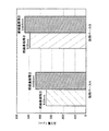
図2は半田の固相線温度と放熱ベースの反り量の関係を示す図である。図2において、横軸は固相線温度(℃)を表し、縦軸は放熱ベースの反り量(μm)を表している。
ここでは、放熱ベースとして、縦43mm×横90mm×厚さ3mmの銅製で反りを与えていない平坦な放熱ベースAと、縦59.6mm×横119.6mm×厚さ3mmの銅製で反りを与えていない平坦な放熱ベースBの2種類のサンプルを用いた。そして、それぞれのサンプルについて、各種組成の鉛フリー半田を用い、アルミナを主成分とする基板の表裏面に銅箔を接合した同じ構造の絶縁基板を半田付けし、そのときの最終的な反り量を測定した。なお、図2中、放熱ベースAを用いた場合を黒塗りで示し、放熱ベースBを用いた場合を白抜きで示している。
FIG. 2 is a diagram showing the relationship between the solidus temperature of solder and the amount of warping of the heat dissipation base. In FIG. 2, the horizontal axis represents the solidus temperature (° C.), and the vertical axis represents the amount of warp (μm) of the heat dissipation base.
Here, as the heat dissipation base, 43 mm long x 90 mm wide x 3 mm thick copper heat dissipating base A and 59.6 mm long x 119.6 mm wide x 3 mm thick copper warp Two types of flat heat-dissipating base B were used. For each sample, lead-free solders of various compositions were used to solder an insulating substrate with the same structure in which copper foil was bonded to the front and back surfaces of the substrate mainly composed of alumina, and the final warpage amount at that time Was measured. In FIG. 2, the case where the heat dissipation base A is used is shown in black, and the case where the heat dissipation base B is used is shown in white.
反り量は、平坦な状態を0μmとし、半田付け後にそこから放熱ベースA,Bの端が移動した距離で評価した。ここでは放熱ベースA,Bの最上端を基準にし、それらの端の移動方向をマイナス方向としている。また、スズ−インジウム系半田については、その組成比を変更して固相線温度を変化させている。図2中、半田組成を示す元素の前に付した数値は、その元素の含有量(%)を表したものであり、例えば、Sn−20Inと表される半田は、その組成に20%のインジウムを含んでいることを表している。 The amount of warpage was evaluated based on the distance traveled by the ends of the heat dissipation bases A and B after soldering, with the flat state being 0 μm. Here, the uppermost ends of the heat dissipating bases A and B are used as a reference, and the moving direction of these ends is the negative direction. In addition, for the tin-indium solder, the composition ratio is changed to change the solidus temperature. In FIG. 2, the numerical value given before the element indicating the solder composition represents the content (%) of the element. For example, the solder represented by Sn-20In has 20% of the composition. It indicates that it contains indium.
図2には、接合に用いた各鉛フリー半田の固相線温度に対する放熱ベースA,Bの反り量をプロットしている。図2より、放熱ベースA,B共、固相線温度が低くなるほど反り量が少なくなる傾向が認められた。特にスズ−インジウム系半田の場合、インジウム含有量が5%,15%,20%と増加するのに伴い、固相線温度が低下し、放熱ベースA,Bの反り量が少なくなる。また、放熱ベースAの場合の方が放熱ベースBの場合に比べて反り量は少なく、放熱ベースAを用いた場合には、組成がSn−SbやSn−Agで表される鉛フリー半田を用いた場合にも反り量を少なく抑えることができる。このように、融点が250℃を下回るような鉛フリー半田を用いた場合、鉛フリー半田が低融点になるほど半田付け後に放熱ベースA,Bに生じる反り量は少なくなる。
FIG. 2 plots the amounts of warpage of the heat dissipation bases A and B with respect to the solidus temperature of each lead-free solder used for bonding. 2. From FIG. 2, it was recognized that the amount of warpage tends to decrease as the solidus temperature decreases for both heat dissipation bases A and B. In particular, in the case of tin-indium solder, as the indium content increases to 5%, 15%, and 20%, the solidus temperature decreases and the amount of warpage of the heat dissipation bases A and B decreases. Further, the amount of warpage is less in the case of the heat dissipation base A than in the case of the heat dissipation base B, and when the heat dissipation base A is used, lead-free solder whose composition is represented by Sn-Sb or Sn-Ag is used. Even when it is used, the amount of warpage can be reduced. Thus, if the melting point using a lead-free solder, such as below 250 ° C., the amount of warpage of the lead-free solder is caused to the heat radiating base A, B after soldering enough to the low melting point that a few.
換言すれば、上記パワー半導体モジュール1を形成する場合においては、低融点の鉛フリー半田を用いるほど半田付け時に加える熱を低くすることができるので、放熱ベース6にあらかじめ与えておく反り量を少なくすることできる。それにより、大きな反りを与えた放熱ベース6を高温で処理して平坦になるように変形させるよりも、最終的に放熱ベース6を平坦か平坦に近い状態に制御しやすくなる。したがって、放熱ベース6が絶縁基板2側へ大きく凸状に反ってしまうのを防止することが可能になる。
In other words, when the
また、図3は鉛フリー半田を用いたときのヒートショック試験の結果を示す図である。図3において、横軸はヒートショックサイクル数(回)を表し、縦軸は放熱ベースと絶縁基板の半田接合部コーナーからのクラック長さ(mm)を表している。 Moreover, FIG. 3 is a figure which shows the result of the heat shock test when lead-free solder is used. In FIG. 3, the horizontal axis represents the number of heat shock cycles (times), and the vertical axis represents the crack length (mm) from the solder joint corner of the heat dissipation base and the insulating substrate.
ここでは、上記図2で述べた放熱ベースAと絶縁基板とを、同じく図2に示したSn−Ag,Sn−Sb,Sn−Ag−Bi−Inの3種の鉛フリー半田でそれぞれ接合したサンプルに対してヒートショック試験を行った。ヒートショック試験は、マイナス40℃での5分間保持と125℃での5分間保持とを途中常温での1分間保持を挟んで繰り返すことによって行った。なお、ヒートショック試験は、液槽式ヒートショック試験装置を使用し、その際の昇温・降温速度は50℃/minとした。 Here, the heat dissipation base A and the insulating substrate described in FIG. 2 are joined with three types of lead-free solders of Sn—Ag, Sn—Sb, and Sn—Ag—Bi—In shown in FIG. The sample was subjected to a heat shock test. The heat shock test was performed by repeating the holding at minus 40 ° C. for 5 minutes and the holding at 125 ° C. for 5 minutes with the holding for 1 minute at room temperature in between. In addition, the heat shock test used the liquid tank type heat shock test apparatus, and the temperature increase / decrease rate in that case was 50 degrees C / min.
図3より、組成がSn−Agで表される鉛フリー半田を用いた場合に比べ、組成がSn−Sb,Sn−Ag−Bi−Inで表される鉛フリー半田を用いた場合には、放熱ベースAと絶縁基板の間の半田接合部に生じるクラックの長さが短くなる傾向が認められた。特に組成がSn−Ag−Bi−Inで表される鉛フリー半田を用いた場合には、300回のヒートショックサイクル後にもクラックが発生していなかった。このように、インジウムやアンチモンを含有したスズ系の鉛フリー半田を用いることにより、半田接合部のクラック耐性を向上させることが可能になる。 From FIG. 3, when using a lead-free solder whose composition is represented by Sn-Sb, Sn-Ag-Bi-In, compared to the case where a lead-free solder whose composition is represented by Sn-Ag is used, The tendency for the length of the crack which arises in the solder joint part between the thermal radiation base A and an insulated substrate to become short was recognized. In particular, when a lead-free solder having a composition represented by Sn—Ag—Bi—In was used, no cracks were generated even after 300 heat shock cycles. Thus, the use of tin-based lead-free solder containing indium or antimony can improve the crack resistance of the solder joint.
例えば、上記パワー半導体モジュール1において、半田層5に生じたクラックが絶縁基板2上に接合される半導体チップ4の直下にまで到達してしまったような場合には、半導体チップ4から放熱ベース6側への伝熱効率が低下してしまい、半導体チップ4の温度上昇が起こって製品寿命が短くなる場合がある。クラック耐性を向上させることにより、製品の長寿命化を図ることが可能になる。なお、このような一定の組成を有する鉛フリー半田を用いたときのクラック耐性向上の効果は、勿論、絶縁基板2と半導体チップ4の間に形成される半田層3についても同様に得られる。
For example, in the
以上述べたように、パワー半導体モジュール1の絶縁基板2と放熱ベース6との接合に鉛フリー半田を用いる場合には、放熱ベース6にあらかじめ凹状の反りを与えておく。また、それと共に、形成するパワー半導体モジュール1の要求特性等に応じ、用いる鉛フリー半田の組成を適当に選定する。それにより、放熱ベース6の絶縁基板2側への大きな凸状の反りの発生を抑制して冷却フィンとの間に大きな隙間を作らず、また、半田層5でのクラックの発生を抑制して、両者の熱的・電気的接続を確保することができるようになる。また、パワー半導体モジュール1の半導体チップ4と絶縁基板2との接合にも鉛フリー半田を用いることにより、半田層3でのクラックの発生を抑制し、両者の熱的・電気的接続を確保することができるようになる。したがって、高性能、高信頼性、長寿命のパワー半導体モジュール1を実現することが可能になる。
As described above, when lead-free solder is used for joining the insulating
さらに、絶縁基板2と放熱ベース6との接合および半導体チップ4と絶縁基板2との接合に鉛フリー半田を用いるため、たとえこのパワー半導体モジュール1が屋外に放置されたような場合でも、鉛の溶出を防止することができる。
Furthermore, since lead-free solder is used for the bonding between the insulating
以下では、上記のようなパワー半導体モジュール1を形成する上で、その放熱ベース6の反り量に影響を及ぼす種々の要素について検討する。
まず、絶縁基板2と放熱ベース6との間の接合面積が放熱ベース6の反り量に及ぼす影響について説明する。
Below, when forming the
First, the influence of the bonding area between the insulating
図4は絶縁基板と放熱ベースとの間の接合面積と放熱ベースの反り量の関係を示す図である。図4において、横軸は接合面積(mm2)を表し、縦軸は放熱ベースの反り量(μm)を表している。 FIG. 4 is a diagram showing the relationship between the bonding area between the insulating substrate and the heat dissipation base and the amount of warpage of the heat dissipation base. In FIG. 4, the horizontal axis represents the bonding area (mm 2 ), and the vertical axis represents the amount of warp (μm) of the heat dissipation base.
図4には、あらかじめ凹状の反りを与えていない平坦な銅製の放熱ベースに鉛フリー半田を用いて各絶縁基板a〜fを接合した場合の放熱ベースに生じる各絶縁基板a〜f側への凸状の反りの量を測定した結果を示している。 In FIG. 4, when the insulating substrates a to f are joined to a flat copper heat radiating base that has not been given a concave warp in advance using lead-free solder, The result of measuring the amount of convex warpage is shown.
絶縁基板a〜fは、最も接合面積が小さくなる平面正方形形状の絶縁基板aを基準に、縦横方向の長さの比率を一定にして面積を増加させた平面正方形形状の絶縁基板b,c、短手方向の長さを一定にして長手方向の長さを増加させた平面長方形形状の絶縁基板d,e、絶縁基板eに対して長手方向の長さを一定にして短手方向の長さを増加させた平面長方形形状の絶縁基板f、という関係を有している。なお、絶縁基板b,dは、長手方向の長さが同じで短手方向の長さが異なっており、同様に、絶縁基板e,f,cは、長手方向の長さが同じで短手方向の長さが異なっている。また、絶縁基板b,fは、短手方向の長さが同じで長手方向の長さが異なっている。 The insulating substrates a to f are planar square-shaped insulating substrates b, c having an increased area with a constant ratio of lengths in the vertical and horizontal directions with reference to the planar square-shaped insulating substrate a having the smallest bonding area. Insulating substrates d and e having a rectangular shape in which the length in the short direction is kept constant and the length in the longitudinal direction is increased, and the length in the short direction is made constant with respect to the insulating substrate e. Insulating substrate f having a planar rectangular shape with an increased number of. The insulating substrates b and d have the same length in the longitudinal direction and different lengths in the short direction. Similarly, the insulating substrates e, f, and c have the same length in the longitudinal direction and are short. The direction lengths are different. Further, the insulating substrates b and f have the same length in the short side direction but different lengths in the long side direction.
各絶縁基板a〜fと放熱ベースとの接合には同種の鉛フリー半田を用いた。また、放熱ベースは、厚みが3mmで、半田付けする各絶縁基板a〜fの平面サイズに応じた平面サイズのものを使用した。ここでは、放熱ベースが平坦なときにその端から半田付けする各絶縁基板a〜fの端までの距離が10mmになる平面サイズの放熱ベースを用いた。半田付け後の放熱ベースの反り量は、長手方向の端の平坦な状態からの移動量で評価した。ここでは、その移動方向をプラス方向としている。 The same kind of lead-free solder was used for joining each of the insulating substrates a to f and the heat dissipation base. Further, the heat radiation base having a thickness of 3 mm and a plane size corresponding to the plane size of each of the insulating substrates a to f to be soldered was used. Here, when the heat dissipating base is flat, a planar heat dissipating base having a distance of 10 mm from the end of each of the insulating substrates a to f to be soldered is used. The amount of warpage of the heat dissipation base after soldering was evaluated by the amount of movement from the flat state at the end in the longitudinal direction. Here, the moving direction is a positive direction.
図4より、まず、絶縁基板a,b,cについて、接合面積の放熱ベース反り量への影響を見ると、接合面積の増加に伴って反り量が比例的に増加していく傾向が認められた。絶縁基板a,d,eについて、接合面長手方向の長さの放熱ベース反り量への影響を見ると、長手方向の長さの増加に伴って反り量が比例的に増加していく傾向が認められた。また、絶縁基板e,f,cについて、接合面短手方向の長さの放熱ベース反り量への影響を見ると、短手方向の長さの増加に伴って反り量が増加していく傾向が認められた。このように、絶縁基板a〜fと放熱ベースとの接合に鉛フリー半田を用いた際の放熱ベースの反り量は、絶縁基板a〜fの接合面積に大きく影響されることがわかる。 From FIG. 4, first, regarding the insulating substrates a, b, and c, when the influence of the junction area on the heat dissipation base warpage amount is observed, the warpage amount tends to increase proportionally as the junction area increases. It was. Regarding the insulating substrates a, d, and e, when the influence of the length in the longitudinal direction of the joint surface on the heat dissipation base warpage amount is observed, the warpage amount tends to increase proportionally with the increase in the length in the longitudinal direction. Admitted. In addition, regarding the insulating substrates e, f, and c, when looking at the influence of the length in the short side of the joint surface on the heat dissipation base warpage, the amount of warpage tends to increase as the length in the short side increases. Was recognized. Thus, it can be seen that the amount of warpage of the heat dissipation base when lead-free solder is used for bonding the insulating substrates af to the heat dissipation base is greatly affected by the bonding area of the insulating substrates af.
換言すれば、パワー半導体モジュール1を形成する場合においては、この結果を用い、鉛フリー半田を用いて接合する絶縁基板2のサイズに応じて放熱ベース6にあらかじめ与えておく反り量を設定することが可能になる。それにより、最終的に放熱ベース6を平坦か平坦に近い状態に制御しやすくなり、放熱ベース6が絶縁基板2側へ大きく凸状に反ってしまうのを防止することが可能になる。
In other words, when the
なお、この図4に示した傾向は、鉛フリー半田の種類を変更した場合にも同様に認められた。
また、同程度の接合面積の絶縁基板2では、それが分割された状態になっているか否かによっても、放熱ベース6の反り量が変化するようになる。
The tendency shown in FIG. 4 was also recognized when the type of lead-free solder was changed.
Further, in the insulating
図5は絶縁基板の分割が放熱ベースの反り量に及ぼす影響を説明する図である。図5において、横軸は接合面積(mm2)を表し、縦軸は放熱ベースの反り量(μm)を表している。 FIG. 5 is a diagram for explaining the influence of the division of the insulating substrate on the amount of warping of the heat dissipation base. In FIG. 5, the horizontal axis represents the bonding area (mm 2 ), and the vertical axis represents the amount of warp (μm) of the heat dissipation base.
ここでは、上記図4で述べた絶縁基板aを用い、まず、2枚の絶縁基板aを放熱ベースに間隔2mmで横に並べて半田接合したものを形成し、見かけ上絶縁基板dが2等分されて放熱ベースに半田接合された状態を形成した(絶縁基板d´)。同様にして、3枚の絶縁基板aを放熱ベースに間隔2mmで横に並べて半田接合したものを形成し、見かけ上絶縁基板eが3等分されて放熱ベースに半田接合された状態を形成した(絶縁基板e´)。また、4枚の絶縁基板aを放熱ベースに間隔2mmで縦横に並べて半田接合したもの、および2枚の絶縁基板dを放熱ベースに間隔2mmで横に並べて半田接合したものを形成し、見かけ上絶縁基板bが4等分あるいは2等分されて放熱ベースに半田接合された状態を形成した(絶縁基板b´,b´´)。 Here, the insulating substrate a described with reference to FIG. 4 is used, and first, two insulating substrates a are arranged side by side with a heat radiation base and soldered together with a spacing of 2 mm, and the insulating substrate d is apparently divided into two equal parts. As a result, a state of being soldered to the heat dissipation base was formed (insulating substrate d ′). In the same manner, three insulating substrates a were arranged side by side on a heat dissipation base and soldered together at an interval of 2 mm, and apparently the insulating substrate e was divided into three equal parts and soldered to the heat dissipation base. (Insulating substrate e ′). In addition, four insulating substrates a are vertically and horizontally soldered to the heat dissipation base with a spacing of 2 mm, and two insulating substrates d are soldered to the heat dissipation base with a distance of 2 mm and solder bonded. The insulating substrate b was divided into four equal parts or two equal parts to form a state where it was soldered to the heat dissipation base (insulating substrates b ′, b ″).
上記図4同様、各絶縁基板d´,e´,b´,b´´と放熱ベースとの接合には同種の鉛フリー半田を用いた。また、放熱ベースは、厚みが3mmで、半田付けする各絶縁基板d´,e´,b´,b´´の平面サイズに応じた平面サイズのものを用いた。ここでは、放熱ベースが平坦なときにその端から各絶縁基板d´,e´,b´,b´´の端までの距離が10mmになる平面サイズの放熱ベースを用いた。半田付け後の放熱ベースの反り量は、長手方向の端の平坦な状態からの移動量で評価した。 As in FIG. 4 above, the same kind of lead-free solder was used to join each of the insulating substrates d ′, e ′, b ′, b ″ and the heat dissipation base. Further, the heat radiation base having a thickness of 3 mm and having a planar size corresponding to the planar size of each of the insulating substrates d ′, e ′, b ′, b ″ to be soldered was used. Here, a planar heat dissipation base is used in which the distance from the end of each heat insulating base to the ends of the insulating substrates d ′, e ′, b ′, b ″ is 10 mm when the heat dissipating base is flat. The amount of warpage of the heat dissipation base after soldering was evaluated by the amount of movement from the flat state at the end in the longitudinal direction.
図5より、絶縁基板d´,e´,b´,b´´のいずれの場合にも、対応するそれぞれの絶縁基板d,e,bに比べ、放熱ベースの反り量が大幅に減少することがわかる。なお、この図5に示した傾向は、鉛フリー半田の種類を変更した場合にも同様に認められた。 From FIG. 5, in any case of the insulating substrates d ′, e ′, b ′, b ″, the amount of warping of the heat dissipation base is greatly reduced as compared with the corresponding insulating substrates d, e, b. I understand. The tendency shown in FIG. 5 was also recognized when the type of lead-free solder was changed.
このように、パワー半導体モジュール1を形成する際には、絶縁基板2と放熱ベース6との間の接合面積が同じ場合でも、絶縁基板2が分割された状態で接合されるか否かに応じて、放熱ベース6にあらかじめ与えておく反り量を設定することが可能になる。
Thus, when the
図6は絶縁基板の設計方法の説明図である。
ここでは、絶縁基板の短手方向の長さの最大値を50mm、長手方向の長さ(複数の絶縁基板を並べて配置する場合には各絶縁基板の長手方向の長さの総和)の最大値を85mmとした場合に、上記図4および図5に示したような測定データを基に、厚さ3mmの放熱ベースに発生する反り量が250μm以下となる絶縁基板サイズを計算によって求めた結果を図示している。なお、絶縁基板のアルミナを主成分とする基板および銅箔の厚さはいずれも0.25mmとした。
FIG. 6 is an explanatory diagram of a method for designing an insulating substrate.
Here, the maximum value of the length of the insulating substrate in the short direction is 50 mm, and the maximum value of the length in the longitudinal direction (when a plurality of insulating substrates are arranged side by side, the sum of the lengths in the longitudinal direction of the insulating substrates) When the thickness is 85 mm, based on the measurement data as shown in FIGS. 4 and 5 above, the result of calculating the insulating substrate size by which the amount of warpage generated in the heat dissipation base with a thickness of 3 mm is 250 μm or less is calculated. It is shown. In addition, the thickness of the board | substrate which has an alumina as a main component of an insulating board | substrate, and copper foil was 0.25 mm.
反り量が250μm以下となるときの絶縁基板の最大サイズは、絶縁基板を1枚使った場合には50mm×50mm、絶縁基板を2枚使った場合には70mm×46mm(絶縁基板1枚のサイズ:35mm×46mm)、絶縁基板を3枚使った場合には85mm×43mm(絶縁基板1枚のサイズ:28mm×43mm)になった。 The maximum size of the insulating substrate when the warp amount is 250 μm or less is 50 mm × 50 mm when one insulating substrate is used, and 70 mm × 46 mm when two insulating substrates are used (the size of one insulating substrate). : 35 mm × 46 mm), and when three insulating substrates were used, the size was 85 mm × 43 mm (size of one insulating substrate: 28 mm × 43 mm).
したがって、パワー半導体モジュール1を形成する場合には、この図6に示したようなデータを用いて絶縁基板2のサイズや分割数を規定することにより、放熱ベース6にあらかじめ与えておく反り量を適切に設定することが可能になる。さらに、絶縁基板2の最大サイズに応じたサイズのパワー半導体モジュール1を形成することが可能になる。絶縁基板2のサイズを大きくした場合には、半導体チップ4の実装数を増やすことが可能になり、また、導体層2b,2cの設計自由度を増すことも可能になる。
Therefore, when the
次に、絶縁基板2の導体層2b,2cの厚さが放熱ベース6の反り量に及ぼす影響について説明する。
パワー半導体モジュール1を形成する場合には、鉛フリー半田による半田付け前に放熱ベース6に凹状の反りを与えておくため、半田付け時には、平坦な絶縁基板2と放熱ベース6との間にできる空間が多少大きくなる。
Next, the influence of the thickness of the conductor layers 2b and 2c of the insulating
When the
図7は半田付け時の絶縁基板と放熱ベースの要部断面模式図である。
上記のように導体層2b,2cの厚みを適当に調整する、例えばこの図7に示すように導体層2cを導体層2bよりも厚く形成することにより、鉛フリー半田による半田付け処理時には、絶縁基板2が放熱ベース6側へ反り、放熱ベース6にあらかじめ与えられている凹状の反りとの間の空間が減少するようになる。そして、半田付け後には、絶縁基板2は平坦な形状に戻り、一方、放熱ベース6は平坦か平坦に近い形状に変形するようになる。その結果、絶縁基板2と放熱ベース6との間にできる空間が減るため、半田層5に半田量が不足する部分が生じることがなく、未接合部分の発生を抑えることが可能になる。
FIG. 7 is a schematic cross-sectional view of the main part of the insulating substrate and the heat dissipation base during soldering.
As described above, the thicknesses of the conductor layers 2b and 2c are appropriately adjusted. For example, the
なお、導体層2b,2cは、用いる銅箔の厚みが厚い方が絶縁基板2と放熱ベース6との熱膨張係数差を小さくするように寄与するため、放熱ベース6の絶縁基板2側への大きな凸状の反りの発生を抑制することが可能になる。
The conductor layers 2b and 2c contribute to reducing the difference in thermal expansion coefficient between the insulating
図8は銅箔の厚さと放熱ベースの反り量の関係を示す図である。図8において、横軸は絶縁基板表裏面に形成した銅箔の厚さ(mm)を表し、縦軸は放熱ベースの反り量(μm)を表している。 FIG. 8 is a diagram showing the relationship between the thickness of the copper foil and the amount of warpage of the heat dissipation base. In FIG. 8, the horizontal axis represents the thickness (mm) of the copper foil formed on the front and back surfaces of the insulating substrate, and the vertical axis represents the amount of warp (μm) of the heat dissipation base.
ここでは、アルミナを主成分とする基板の厚さが共通で銅箔の厚さが異なる絶縁基板を使用し、放熱ベースには、上記図2で述べた放熱ベースAを用いた。なお、各絶縁基板の表裏面の銅箔は同じ厚さにした。また、絶縁基板と放熱ベースAの接合には、同種の鉛フリー半田を使用した。半田付け後の放熱ベースの反り量は、長手方向の端の平坦な状態からの移動量で評価した。 Here, an insulating substrate having a common thickness of the substrate mainly composed of alumina and a different thickness of the copper foil was used, and the heat radiating base A described in FIG. 2 was used as the heat radiating base. The copper foils on the front and back surfaces of each insulating substrate had the same thickness. The same kind of lead-free solder was used for joining the insulating substrate and the heat dissipation base A. The amount of warpage of the heat dissipation base after soldering was evaluated by the amount of movement from the flat state at the end in the longitudinal direction.
図8より、アルミナを主成分とする基板に形成される銅箔の厚さが0.4mmを超える領域で放熱ベースAの反り量が減少することがわかる。このように、アルミナを主成分とする基板に形成する銅箔を厚くして絶縁基板と放熱ベースAとの熱膨張係数差を小さくすることにより、放熱ベースAの反りを少なくすることができる。なお、この図8に示した傾向は、鉛フリー半田の種類を変更した場合にも同様に認められた。 FIG. 8 shows that the amount of warping of the heat dissipation base A decreases in the region where the thickness of the copper foil formed on the substrate mainly composed of alumina exceeds 0.4 mm. Thus, the warp of the heat dissipation base A can be reduced by increasing the thickness of the copper foil formed on the substrate mainly composed of alumina to reduce the difference in thermal expansion coefficient between the insulating substrate and the heat dissipation base A. The tendency shown in FIG. 8 was also recognized when the type of lead-free solder was changed.
このように、あらかじめ凹状の反りを与えられた放熱ベース6を用いてパワー半導体モジュール1を形成する際には、導体層2bに比べて導体層2cを厚く形成する、あるいは導体層2b,2cを0.4mmを超えるような厚さで形成することにより、絶縁基板2と放熱ベース6との間の未接合部分の発生を抑えると共に、放熱ベース6が凹状から平坦な状態になった後にさらに絶縁基板2側へ大きく凸状に反ってしまうのを抑えることが可能になる。また、放熱ベース6にあらかじめ与えておく反り量を少なく設定することも可能になる。
Thus, when the
なお、導体層2bの厚さは、導体層2b上に接合される半導体チップ4に所望の電流を流しうる厚さを勘案し、さらに、導体層2b,2cの厚さは上記のような熱膨張係数差、セラミック基板2aの材質や厚さを考慮して、その厚さを0.4mm以上でできるだけ厚くすることが好ましい。セラミック基板2aへの導体層2b,2cの接合性は、セラミック基板2aの材質や厚さにもよるが、例えばセラミック基板2aに窒化珪素を主成分とする基板を用いた場合には0.8mmより厚い導体層2b,2cを接合することが可能であり、アルミナを主成分とする基板についても同様に0.8mmより厚い導体層2b,2cを接合することが可能である。
The thickness of the
また、ここでは絶縁基板2の導体層2b,2cの厚さに着目したが、導体層2b,2cの体積に着目し、その比を適当に設定するようにしてもよい。例えば、導体層2bの体積に対する導体層2cの体積の比が1以上になるようにする。このような体積比であれば、導体層2b,2cのパターン形状によっては、導体層2bよりも導体層2cの方が厚い場合のほか、導体層2b,2cの厚さが同じかあるいは導体層2bの方が厚い場合でも、上記のような未接合部分の発生や放熱ベース6の大きな凸状の反りの発生を抑えることが可能になると共に、放熱ベース6にあらかじめ与えておく反り量を少なく設定することが可能になる。
Here, the thickness of the conductor layers 2b and 2c of the insulating
次に、絶縁基板2のセラミック基板2aの厚さが放熱ベース6の反り量に及ぼす影響について説明する。
上記のように絶縁基板2を構成する導体層2b,2cの厚さを適当に設定するのと同様の考え方から、セラミック基板2aの厚さを薄くすることによって、絶縁基板2と放熱ベース6との熱膨張係数差を小さくするようにしてもよい。
Next, the influence of the thickness of the
From the same idea as setting the thicknesses of the conductor layers 2b and 2c constituting the insulating
図9はセラミック基板の厚さと放熱ベースの反り量の関係を示す図である。図9において、縦軸は放熱ベースの反り量(μm)を表している。
ここでは、放熱ベースとして、上記図2で述べた2種類の放熱ベースA,Bであらかじめ凹状の反りは与えていない平坦なものを用いた。絶縁基板には、厚さ0.25mm,0.32mm,0.635mmの各アルミナを主成分とする基板に、厚さが共通の銅箔を形成した絶縁基板を用いた。これらの放熱ベースA,Bと絶縁基板の接合には、同種の鉛フリー半田を用いた。半田付け後の放熱ベースの反り量は、長手方向の端の平坦な状態からの移動量で評価した。
FIG. 9 is a diagram showing the relationship between the thickness of the ceramic substrate and the amount of warping of the heat dissipation base. In FIG. 9, the vertical axis represents the amount of warp (μm) of the heat dissipation base.
Here, as the heat radiating base, two types of heat radiating bases A and B described with reference to FIG. As the insulating substrate, an insulating substrate in which a copper foil having a common thickness was formed on a substrate mainly composed of alumina having thicknesses of 0.25 mm, 0.32 mm, and 0.635 mm was used. The same kind of lead-free solder was used for joining the heat dissipation bases A and B and the insulating substrate. The amount of warpage of the heat dissipation base after soldering was evaluated by the amount of movement from the flat state at the end in the longitudinal direction.
図9より、いずれの放熱ベースA,Bの場合でも、アルミナを主成分とする基板の厚さが薄くなることで、その反り量が減少することがわかる。このように、アルミナを主成分とする基板を薄くして絶縁基板と放熱ベースA,Bとの熱膨張係数差を小さくすることにより、放熱ベースA,Bの反りを少なくすることができる。特にアルミナを主成分とする基板は、セラミックの中でも熱膨張係数が比較的金属の熱膨張係数に近く(約8ppm/K)、放熱ベースA,Bの反りを少なくする点で有効である。なお、この図9に示した傾向は、鉛フリー半田の種類を変更した場合でも同様であった。 From FIG. 9, it can be seen that, in any of the heat dissipation bases A and B, the amount of warpage decreases as the thickness of the substrate mainly composed of alumina is reduced. As described above, the warp of the heat dissipation bases A and B can be reduced by thinning the substrate mainly composed of alumina and reducing the difference in thermal expansion coefficient between the insulating substrate and the heat dissipation bases A and B. In particular, a substrate mainly composed of alumina is effective in that the thermal expansion coefficient is relatively close to that of a metal (about 8 ppm / K) among ceramics and the warping of the heat dissipation bases A and B is reduced. The tendency shown in FIG. 9 was the same even when the type of lead-free solder was changed.
このように、パワー半導体モジュール1を形成する際には、セラミック基板2aであるアルミナを主成分とする基板の厚さを適当に設定して絶縁基板2を形成することにより、絶縁基板2と放熱ベース6との未接合部分の発生を抑えると共に、放熱ベース6が絶縁基板2側へ大きく凸状に反ってしまうのを抑えることが可能になる。絶縁基板2のセラミック基板2aとして窒化珪素を主成分とする基板を用いた場合にも同様のことが言える。
Thus, when the
なお、絶縁基板2のセラミック基板2aは、未接合部分の発生と放熱ベース6の絶縁基板2側への反りの発生を抑えることに加え、伝熱効率および絶縁基板2自体の強度を一定以上に保つ必要性を考慮し、その厚さを0.635mm以下とするのが好ましく、さらには、セラミック基板2aの熱伝導等を勘案すると、0.2mm〜0.4mmの範囲とすることが好ましい。図9に示したように、セラミック基板2aの厚さが0.635mmの場合には、厚さが0.25mm,0.32mmの場合に比べるとその反り量は大きくなるが、放熱ベース6の形態を適当に選択すれば、絶縁基板2と放熱ベース6との未接合部分の発生を抑え、さらに放熱ベース6が絶縁基板2側へ大きく凸状に反ってしまうのを抑えることは可能である。
The
次に、放熱ベース6の厚さがその反り量に及ぼす影響について説明する。
図10は放熱ベースの厚さとその反り量の関係を示す図である。図10において、横軸は半田付け処理の際の温度(℃)を表し、縦軸は放熱ベースの反り量(μm)を表している。
Next, the effect of the thickness of the
FIG. 10 is a diagram showing the relationship between the thickness of the heat dissipation base and the amount of warpage thereof. In FIG. 10, the horizontal axis represents the temperature (° C.) during the soldering process, and the vertical axis represents the amount of warp (μm) of the heat dissipation base.
ここでは、放熱ベースとして同一平面サイズで厚さが2mm,3mm,4mmのものを用い、これを鉛フリー半田を用いた通常の半田付け条件と同様の条件で熱処理したときの各温度での反り量を測定した。反り量は、放熱ベースの最上端を基準(0μm)にし、その端の移動方向をマイナス方向としたときの移動量で評価した。 Here, the heat dissipation bases with the same plane size and thickness of 2 mm, 3 mm, and 4 mm are used, and the warp at each temperature when heat-treated under the same conditions as the normal soldering conditions using lead-free solder The amount was measured. The amount of warpage was evaluated by the amount of movement when the uppermost end of the heat dissipating base was the reference (0 μm) and the moving direction of the end was the minus direction.
図10より、放熱ベースが厚くなるほど温度に対する反り量の変化は小さく、温度30℃での反り量、すなわち半田付け後の反り量は、最も薄い2mmの放熱ベースで最大になり、最も厚い4mmの放熱ベースで最小になった。このように、放熱ベースは、厚くなるほど反り量が少なくなることがわかる。特に、放熱ベースの厚さが3mm以上の場合には反りを比較的小さく抑えることができ、あらかじめ与えておく反り量を少なく設定することが可能になる。 From FIG. 10, as the heat radiation base becomes thicker, the change in the warpage amount with respect to the temperature becomes smaller. The warpage amount at a temperature of 30 ° C., that is, the warpage amount after soldering becomes the maximum with the thinnest 2 mm heat radiation base, The heat dissipation base is minimized. Thus, it turns out that the amount of curvature decreases as the heat dissipation base becomes thicker. In particular, when the thickness of the heat dissipating base is 3 mm or more, the warpage can be suppressed to be relatively small, and the amount of warpage given in advance can be set small.
このように、あらかじめ凹状の反りを与えられた放熱ベース6を用いてパワー半導体モジュール1を形成する際には、放熱ベース6は厚い方があらかじめ与えておく反り量を少なく設定することができ、放熱ベース6が絶縁基板2側へ大きく凸状に反ってしまうのを防止することが可能になる。なお、放熱ベース6は、パワー半導体モジュール1の形成上、発生する反りの大きさ、平坦か平坦に近い状態へのしやすさ、パワー半導体モジュール1のサイズ等を考慮し、その厚さを3mm〜4mmの範囲とすることが好ましい。ただし、放熱ベース6の厚さが3mmを下回るような場合であっても、絶縁基板2側の形態を適当に選択すれば、あらかじめ与えておく反り量を少なくして放熱ベース6が絶縁基板2側へ大きく凸状に反ってしまうのを防止することは可能である。パワー半導体モジュール1の形成上は、この点も考慮し、放熱ベース6の厚さを2mm〜4mmの範囲とすることができる。
Thus, when the
以上述べたように、鉛フリー半田を用いてパワー半導体モジュール1を形成する際には、放熱ベース6の反り量に影響を及ぼす種々の要素、すなわち絶縁基板2の形態(放熱ベース6との接合面積、分割状態、導体層2b,2cの厚さ、セラミック基板2aの厚さ)や放熱ベース6の形態(平面サイズ、厚さ)に応じて、放熱ベース6にあらかじめ与えておく反り量を設定することができる。そして、この反り量を適切に設定することにより、絶縁基板2と放熱ベース6との間の未接合部の発生や放熱ベース6と冷却フィンとの間の大きな隙間の発生が抑えられた、クラック耐性が高く、さらに鉛溶出のない、高性能、高信頼性、長寿命のパワー半導体モジュール1が実現される。
As described above, when the
最後に、放熱ベース6の形成方法について説明する。
放熱ベース6は、プレス型を用いて形成することができる。反りを与えて放熱ベース6を形成する場合には、与える反りに応じた形状のプレス型を用意し、それを用いて形成する。例えば、銅製の放熱ベース6を形成する場合、所定形状のプレス型内に銅粉末を充填してこれをプレスすることによって成型体を形成し、さらに、この成型体を不活性ガス雰囲気中等で熱処理する。これにより、プレス型に応じた形状の放熱ベース6が形成される。このような方法によれば、プレス型を変更することにより、機械的な加工を行わずに、様々な反り量および平面サイズの放熱ベース6を形成することができる。
Finally, a method for forming the
The
以上説明したように、上記構成を有するパワー半導体モジュール1においては、半導体チップ4と絶縁基板2との接合および絶縁基板2と放熱ベース6との接合に鉛フリー半田を用いるようにしたので、環境汚染を防ぐことが可能になる。さらに、それらの接合に鉛フリー半田を用いると共に、放熱ベース6にあらかじめ凹状に反りを与えておいて半田付け後に平坦か平坦に近い状態が得られるようにしたので、放熱ベース6と冷却フィンとの接触熱抵抗を低く抑えることが可能になる。その結果、半導体チップ4の放熱性を確保し、高性能かつ高信頼性のパワー半導体モジュール1が実現可能になる。また、パワー半導体モジュール1の要求特性等に応じ、用いる鉛フリー半田を適当に選択することにより、クラック耐性を向上させ、パワー半導体モジュール1の長寿命化を図れる。
As described above, in the
なお、以上の説明では、主にパワー半導体モジュール1の絶縁基板2と放熱ベース6を鉛フリー半田で接合する場合を例にして述べたが、本発明は、その他の半導体装置において熱膨張係数差が比較的大きい部材間を鉛フリー半田で接合するような場合に同様に適用可能である。
In the above description, the case where the insulating
1 パワー半導体モジュール
2 絶縁基板
2a セラミック基板
2b,2c 導体層
3,5 半田層
4 半導体チップ
6 放熱ベース
DESCRIPTION OF
Claims (9)
前記半導体チップと前記絶縁基板との間および前記絶縁基板と前記放熱ベースとの間が鉛を含まない半田を用いて接合され、かつ、前記放熱ベースが前記鉛を含まない半田を用いて略平坦な状態で接合されており、
前記放熱ベースは、銅を用いて構成され、
前記鉛を含まない半田は、銀、ビスマス、インジウム、アンチモン、亜鉛、アルミニウム、銅のうちの少なくとも1種とスズとを含む、融点が250℃以下の半田であり、
前記絶縁基板は、最大サイズを70mm×46mmとし、2枚に分割された状態で前記放熱ベース上に半田接合され、2枚に分割された各絶縁基板の前記放熱ベースとの接合面積が400mm 2 以上1610mm 2 以下であることを特徴とする半導体装置。 In a semiconductor device having a structure in which an insulating substrate having a conductor layer on both sides of a ceramic substrate is soldered on a heat dissipation base, and a semiconductor chip is soldered on the insulating substrate,
The semiconductor chip and the insulating substrate and between the insulating substrate and the heat dissipation base are joined using solder that does not contain lead, and the heat dissipation base is substantially flat using solder that does not contain lead. Are joined together
The heat dissipation base is configured using copper,
The lead-free solder is a solder containing at least one of silver, bismuth, indium, antimony, zinc, aluminum, copper and a melting point of 250 ° C. or less,
The insulating substrate has a maximum size of 70 mm × 46 mm and is soldered onto the heat radiating base in a state of being divided into two sheets, and the bonding area of each of the two divided substrates to the heat radiating base is 400 mm 2. The semiconductor device is characterized in that it is 1610 mm 2 or less .
前記半導体チップと前記絶縁基板との間および前記絶縁基板と前記放熱ベースとの間が鉛を含まない半田を用いて接合され、かつ、前記放熱ベースが前記鉛を含まない半田を用いて略平坦な状態で接合されており、 The semiconductor chip and the insulating substrate and between the insulating substrate and the heat dissipation base are joined using solder that does not contain lead, and the heat dissipation base is substantially flat using solder that does not contain lead. Are joined together
前記放熱ベースは、銅を用いて構成され、 The heat dissipation base is configured using copper,
前記鉛を含まない半田は、銀、ビスマス、インジウム、アンチモン、亜鉛、アルミニウム、銅のうちの少なくとも1種とスズとを含む、融点が250℃以下の半田であり、 The lead-free solder is a solder containing at least one of silver, bismuth, indium, antimony, zinc, aluminum, copper and a melting point of 250 ° C. or less,
前記絶縁基板は、最大サイズを85mm×43mmとし、3枚に分割された状態で前記放熱ベース上に半田接合され、3枚に分割された各絶縁基板の前記放熱ベースとの接合面積が400mm The insulating substrate has a maximum size of 85 mm × 43 mm and is solder-bonded to the heat dissipation base in a state of being divided into three sheets, and the bonding area of each of the divided insulating substrates to the heat dissipation base is 400 mm. 22 以上1204mm1204 mm 22 以下であることを特徴とする半導体装置。A semiconductor device, wherein:
前記半導体チップと前記絶縁基板との間の半田接合および前記絶縁基板と前記放熱ベースとの間の半田接合のうち少なくとも前記絶縁基板と前記放熱ベースとの間の半田接合に用いられている前記鉛を含まない半田は、スズ、銀、ビスマスおよびインジウムからなる、融点が250℃以下の半田であることを特徴とする請求項1又は2に記載の半導体装置。 The lead used for solder bonding between at least the insulating substrate and the heat dissipation base among solder bonding between the semiconductor chip and the insulating substrate and solder bonding between the insulating substrate and the heat dissipation base. 3. The semiconductor device according to claim 1, wherein the solder containing no solder is a solder composed of tin, silver, bismuth, and indium and having a melting point of 250 ° C. or less.
Priority Applications (7)
| Application Number | Priority Date | Filing Date | Title |
|---|---|---|---|
| JP2005011369A JP4207896B2 (en) | 2005-01-19 | 2005-01-19 | Semiconductor device |
| US11/327,482 US20060157862A1 (en) | 2005-01-19 | 2006-01-09 | Semiconductor device and method for producing the same |
| KR1020060005250A KR101194429B1 (en) | 2005-01-19 | 2006-01-18 | Semiconductor device and method for producing the same |
| DE102006002452.4A DE102006002452B4 (en) | 2005-01-19 | 2006-01-18 | Semiconductor device and method for its production |
| CN200610005457A CN100589243C (en) | 2005-01-19 | 2006-01-18 | Semiconductor device |
| KR1020120009720A KR101402924B1 (en) | 2005-01-19 | 2012-01-31 | Semiconductor device and manufacturing method thereof |
| US14/016,754 US9269644B2 (en) | 2005-01-19 | 2013-09-03 | Method for producing semiconductor device |
Applications Claiming Priority (1)
| Application Number | Priority Date | Filing Date | Title |
|---|---|---|---|
| JP2005011369A JP4207896B2 (en) | 2005-01-19 | 2005-01-19 | Semiconductor device |
Related Child Applications (1)
| Application Number | Title | Priority Date | Filing Date |
|---|---|---|---|
| JP2007338468A Division JP4683043B2 (en) | 2007-12-28 | 2007-12-28 | Manufacturing method of semiconductor device |
Publications (2)
| Publication Number | Publication Date |
|---|---|
| JP2006202884A JP2006202884A (en) | 2006-08-03 |
| JP4207896B2 true JP4207896B2 (en) | 2009-01-14 |
Family
ID=36650778
Family Applications (1)
| Application Number | Title | Priority Date | Filing Date |
|---|---|---|---|
| JP2005011369A Expired - Lifetime JP4207896B2 (en) | 2005-01-19 | 2005-01-19 | Semiconductor device |
Country Status (5)
| Country | Link |
|---|---|
| US (2) | US20060157862A1 (en) |
| JP (1) | JP4207896B2 (en) |
| KR (2) | KR101194429B1 (en) |
| CN (1) | CN100589243C (en) |
| DE (1) | DE102006002452B4 (en) |
Families Citing this family (37)
| Publication number | Priority date | Publication date | Assignee | Title |
|---|---|---|---|---|
| JP5224430B2 (en) * | 2006-03-17 | 2013-07-03 | 株式会社豊田中央研究所 | Power semiconductor module |
| JP2008270485A (en) * | 2007-04-19 | 2008-11-06 | Toyota Industries Corp | Semiconductor device |
| US8253233B2 (en) | 2008-02-14 | 2012-08-28 | Infineon Technologies Ag | Module including a sintered joint bonding a semiconductor chip to a copper surface |
| CN101971329B (en) * | 2008-03-17 | 2012-11-21 | 三菱综合材料株式会社 | Substrate for power module with heat sink and method for producing the same, power module with heat sink, and substrate for power module |
| JP2009283741A (en) * | 2008-05-23 | 2009-12-03 | Fuji Electric Device Technology Co Ltd | Semiconductor device |
| EP2265099B1 (en) * | 2009-06-04 | 2013-11-27 | Honda Motor Co., Ltd. | Semiconductor device and method of manufacturing the same |
| JP5512377B2 (en) | 2010-04-28 | 2014-06-04 | 本田技研工業株式会社 | Circuit board |
| JP5268994B2 (en) * | 2010-05-31 | 2013-08-21 | 三菱電機株式会社 | Semiconductor module and manufacturing method thereof |
| CN102447018A (en) * | 2010-10-12 | 2012-05-09 | 柏腾科技股份有限公司 | Improved combination of substrate and heat dissipation structure and method thereof |
| JP6086863B2 (en) | 2011-06-27 | 2017-03-01 | ローム株式会社 | Semiconductor module |
| CN102856272A (en) * | 2011-06-27 | 2013-01-02 | 北京兆阳能源技术有限公司 | Insulating and radiating electronic subassembly |
| CN102916107A (en) * | 2011-08-05 | 2013-02-06 | 柏腾科技股份有限公司 | Composite cooling plate structure and method for packaging light-emitting diodes using it |
| CN104067502B (en) * | 2012-03-21 | 2016-08-24 | 富士电机株式会社 | Power conversion device |
| JP6044097B2 (en) * | 2012-03-30 | 2016-12-14 | 三菱マテリアル株式会社 | Power module substrate with heat sink, power module substrate with cooler, and power module |
| DE102012205240B4 (en) * | 2012-03-30 | 2016-08-04 | Semikron Elektronik Gmbh & Co. Kg | Method for producing a substrate for at least one power semiconductor component, method for producing a power semiconductor module and power semiconductor module |
| US8941208B2 (en) * | 2012-07-30 | 2015-01-27 | General Electric Company | Reliable surface mount integrated power module |
| US9293291B2 (en) | 2012-08-31 | 2016-03-22 | Samsung Display Co., Ltd. | Flexible display device manufacturing method and carrier substrate for the method |
| CN103887246A (en) * | 2012-12-20 | 2014-06-25 | 浙江大学 | Power electronic module heat radiation structure with novel joint layer |
| JP6085968B2 (en) * | 2012-12-27 | 2017-03-01 | 三菱マテリアル株式会社 | Power module substrate with metal member, power module with metal member, and method for manufacturing power module substrate with metal member |
| JP6111764B2 (en) * | 2013-03-18 | 2017-04-12 | 三菱マテリアル株式会社 | Power module substrate manufacturing method |
| JP5672324B2 (en) | 2013-03-18 | 2015-02-18 | 三菱マテリアル株式会社 | Manufacturing method of joined body and manufacturing method of power module substrate |
| WO2014174854A1 (en) * | 2013-04-25 | 2014-10-30 | 富士電機株式会社 | Semiconductor device |
| JP2015046236A (en) * | 2013-08-27 | 2015-03-12 | 東芝ライテック株式会社 | Light emitting device and lighting device |
| JP2015173215A (en) * | 2014-03-12 | 2015-10-01 | 株式会社東芝 | Semiconductor device and method of manufacturing the same |
| JP6384112B2 (en) * | 2014-04-25 | 2018-09-05 | 三菱マテリアル株式会社 | Power module substrate and power module substrate with heat sink |
| JP6451180B2 (en) * | 2014-09-26 | 2019-01-16 | 富士電機株式会社 | Semiconductor device manufacturing apparatus and semiconductor device |
| WO2018017216A1 (en) * | 2016-07-18 | 2018-01-25 | Applied Materials, Inc. | A method and material for cmos contact and barrier layer |
| WO2018021473A1 (en) * | 2016-07-28 | 2018-02-01 | 株式会社 東芝 | Circuit board and semiconductor module |
| WO2018180159A1 (en) * | 2017-03-29 | 2018-10-04 | 三菱マテリアル株式会社 | Method for producing insulated circuit board with heat sink |
| US11457513B2 (en) | 2017-04-13 | 2022-09-27 | Bradford White Corporation | Ceramic heating element |
| CN108417501B (en) | 2018-03-05 | 2020-03-24 | 台达电子企业管理(上海)有限公司 | Power module and preparation method thereof |
| JP7334464B2 (en) * | 2019-05-15 | 2023-08-29 | 富士電機株式会社 | Semiconductor module, method for manufacturing semiconductor module, and step jig |
| JP7320446B2 (en) * | 2019-12-27 | 2023-08-03 | 株式会社 日立パワーデバイス | Semiconductor device and its manufacturing method |
| US11610861B2 (en) | 2020-09-14 | 2023-03-21 | Infineon Technologies Austria Ag | Diffusion soldering with contaminant protection |
| US11439039B2 (en) | 2020-12-07 | 2022-09-06 | Hamilton Sundstrand Corporation | Thermal management of electronic devices on a cold plate |
| CN113620234B (en) * | 2021-05-28 | 2024-01-12 | 上海曦智科技有限公司 | Chip packaging structure, control method and optical computing device |
| CN113539995B (en) * | 2021-07-16 | 2024-04-12 | 威星国际半导体(深圳)有限公司 | High-thermal-conductivity silicon carbide device packaging structure and method |
Family Cites Families (33)
| Publication number | Priority date | Publication date | Assignee | Title |
|---|---|---|---|---|
| US3829598A (en) * | 1972-09-25 | 1974-08-13 | Hutson Ind Inc | Copper heat sinks for electronic devices and method of making same |
| US4806309A (en) * | 1988-01-05 | 1989-02-21 | Willard Industries, Inc. | Tin base lead-free solder composition containing bismuth, silver and antimony |
| JPH0277143A (en) | 1988-09-13 | 1990-03-16 | Mitsubishi Electric Corp | Semiconductor device |
| US5043796A (en) * | 1990-02-06 | 1991-08-27 | Motorola, Inc. | Isolating multiple device mount with stress relief |
| JPH0496355A (en) * | 1990-08-13 | 1992-03-27 | Meidensha Corp | Manufacture of semiconductor device |
| US5328751A (en) * | 1991-07-12 | 1994-07-12 | Kabushiki Kaisha Toshiba | Ceramic circuit board with a curved lead terminal |
| KR100307465B1 (en) * | 1992-10-20 | 2001-12-15 | 야기 추구오 | Power module |
| US5344607A (en) * | 1993-06-16 | 1994-09-06 | International Business Machines Corporation | Lead-free, high tin, ternary solder alloy of tin, bismuth, and indium |
| US5985212A (en) * | 1996-12-12 | 1999-11-16 | H-Technologies Group, Incorporated | High strength lead-free solder materials |
| US6261703B1 (en) * | 1997-05-26 | 2001-07-17 | Sumitomo Electric Industries, Ltd. | Copper circuit junction substrate and method of producing the same |
| US6060772A (en) * | 1997-06-30 | 2000-05-09 | Kabushiki Kaisha Toshiba | Power semiconductor module with a plurality of semiconductor chips |
| CN1146988C (en) * | 1997-12-08 | 2004-04-21 | 东芝株式会社 | Package for semiconductor power device and method for assembling the same |
| JP2000153388A (en) * | 1998-09-14 | 2000-06-06 | Murata Mfg Co Ltd | Soldered article |
| US6139979A (en) * | 1999-01-28 | 2000-10-31 | Murata Manufacturing Co., Ltd. | Lead-free solder and soldered article |
| WO2002013267A1 (en) * | 2000-08-09 | 2002-02-14 | Mitsubishi Materials Corporation | Power module and power module with heat sink |
| JP4756200B2 (en) * | 2000-09-04 | 2011-08-24 | Dowaメタルテック株式会社 | Metal ceramic circuit board |
| JP2002203942A (en) * | 2000-12-28 | 2002-07-19 | Fuji Electric Co Ltd | Power semiconductor module |
| US6784086B2 (en) * | 2001-02-08 | 2004-08-31 | International Business Machines Corporation | Lead-free solder structure and method for high fatigue life |
| JP2002246515A (en) * | 2001-02-20 | 2002-08-30 | Mitsubishi Electric Corp | Semiconductor device |
| US7069645B2 (en) * | 2001-03-29 | 2006-07-04 | Ngk Insulators, Ltd. | Method for producing a circuit board |
| JP2003046032A (en) * | 2001-07-26 | 2003-02-14 | Hitachi Ltd | Copper composite material heat-radiating board, semiconductor power module and manufacturing method therefor |
| JP4848539B2 (en) * | 2001-08-23 | 2011-12-28 | Dowaメタルテック株式会社 | Heat sink, power semiconductor module, IC package |
| JP2003163315A (en) * | 2001-11-29 | 2003-06-06 | Denki Kagaku Kogyo Kk | module |
| JP3964659B2 (en) * | 2001-11-30 | 2007-08-22 | 松下電器産業株式会社 | Chargeable particles, method for producing the same, and electronic circuit board |
| JP2003198117A (en) * | 2001-12-28 | 2003-07-11 | Matsushita Electric Ind Co Ltd | Soldering method and junction structure body |
| JP2003204020A (en) * | 2002-01-04 | 2003-07-18 | Mitsubishi Electric Corp | Semiconductor device |
| JP4692708B2 (en) * | 2002-03-15 | 2011-06-01 | Dowaメタルテック株式会社 | Ceramic circuit board and power module |
| JP4113971B2 (en) * | 2002-07-30 | 2008-07-09 | 株式会社豊田自動織機 | Low expansion material and manufacturing method thereof |
| JP4121827B2 (en) * | 2002-10-18 | 2008-07-23 | 電気化学工業株式会社 | Method for manufacturing module structure |
| JP2004356625A (en) * | 2003-05-06 | 2004-12-16 | Fuji Electric Device Technology Co Ltd | Semiconductor device and manufacturing method thereof |
| KR100705868B1 (en) * | 2003-05-06 | 2007-04-10 | 후지 덴키 디바이스 테크놀로지 가부시키가이샤 | Semiconductor device and manufacturing method thereof |
| JP4664816B2 (en) * | 2003-09-25 | 2011-04-06 | 株式会社東芝 | Ceramic circuit board, manufacturing method thereof and power module |
| JP4918856B2 (en) * | 2004-04-05 | 2012-04-18 | 三菱マテリアル株式会社 | Power module substrate and power module |
-
2005
- 2005-01-19 JP JP2005011369A patent/JP4207896B2/en not_active Expired - Lifetime
-
2006
- 2006-01-09 US US11/327,482 patent/US20060157862A1/en not_active Abandoned
- 2006-01-18 DE DE102006002452.4A patent/DE102006002452B4/en active Active
- 2006-01-18 KR KR1020060005250A patent/KR101194429B1/en active IP Right Grant
- 2006-01-18 CN CN200610005457A patent/CN100589243C/en active Active
-
2012
- 2012-01-31 KR KR1020120009720A patent/KR101402924B1/en active IP Right Grant
-
2013
- 2013-09-03 US US14/016,754 patent/US9269644B2/en active Active
Also Published As
| Publication number | Publication date |
|---|---|
| DE102006002452A1 (en) | 2006-07-27 |
| US9269644B2 (en) | 2016-02-23 |
| KR101194429B1 (en) | 2012-10-24 |
| US20060157862A1 (en) | 2006-07-20 |
| KR20120032497A (en) | 2012-04-05 |
| JP2006202884A (en) | 2006-08-03 |
| CN1815720A (en) | 2006-08-09 |
| KR101402924B1 (en) | 2014-06-02 |
| KR20060084373A (en) | 2006-07-24 |
| US20140080262A1 (en) | 2014-03-20 |
| DE102006002452B4 (en) | 2014-06-26 |
| CN100589243C (en) | 2010-02-10 |
Similar Documents
| Publication | Publication Date | Title |
|---|---|---|
| JP4207896B2 (en) | Semiconductor device | |
| KR102146589B1 (en) | Substrate for power module with heat sink, power module with heat sink, and method for producing substrate for power module with heat sink | |
| JP5613914B2 (en) | Power module substrate | |
| KR102097177B1 (en) | Power module substrate, power module substrate with heat sink, and power module | |
| JP4683043B2 (en) | Manufacturing method of semiconductor device | |
| US9786577B2 (en) | Power module substrate, heat-sink-attached power-module substrate, and heat-sink-attached power module | |
| JP6111764B2 (en) | Power module substrate manufacturing method | |
| WO2016002803A1 (en) | Substrate unit for power modules, and power module | |
| CN100390977C (en) | Semiconductor device and its manufacturing method | |
| KR20140142256A (en) | Power module substrate with heat sink, power module substrate with cooler, and power module | |
| JP4893095B2 (en) | Circuit board and semiconductor module using the same | |
| JP4893096B2 (en) | Circuit board and semiconductor module using the same | |
| JP2009283741A (en) | Semiconductor device | |
| JPWO2017221730A1 (en) | Power semiconductor device and method for manufacturing power semiconductor device | |
| JP2009272487A (en) | Electronic component | |
| KR20180059778A (en) | A substrate for a light emitting module, a light emitting module, a substrate for a light emitting module formed with a cooler, and a method for manufacturing a substrate for a light emitting module | |
| KR20200135395A (en) | Manufacturing method of electronic component mounting module | |
| JP2004356625A (en) | Semiconductor device and manufacturing method thereof | |
| KR20200135378A (en) | Electronic component mounting module | |
| JP4560645B2 (en) | Heat sink for mounting a plurality of semiconductor substrates and semiconductor substrate assembly using the same | |
| JP5195314B2 (en) | Manufacturing method of semiconductor device | |
| JP2006332084A (en) | Semiconductor device manufacturing method and semiconductor device | |
| JPH10223809A (en) | Power module | |
| WO2023218999A1 (en) | Electronic component with heat dissipating part, and manufacturing method therefor | |
| JP5126073B2 (en) | Manufacturing method of semiconductor device |
Legal Events
| Date | Code | Title | Description |
|---|---|---|---|
| A977 | Report on retrieval |
Free format text: JAPANESE INTERMEDIATE CODE: A971007 Effective date: 20071031 |
|
| A131 | Notification of reasons for refusal |
Free format text: JAPANESE INTERMEDIATE CODE: A131 Effective date: 20071106 |
|
| A521 | Request for written amendment filed |
Free format text: JAPANESE INTERMEDIATE CODE: A523 Effective date: 20071228 |
|
| A131 | Notification of reasons for refusal |
Free format text: JAPANESE INTERMEDIATE CODE: A131 Effective date: 20080129 |
|
| A521 | Request for written amendment filed |
Free format text: JAPANESE INTERMEDIATE CODE: A523 Effective date: 20080331 |
|
| A131 | Notification of reasons for refusal |
Free format text: JAPANESE INTERMEDIATE CODE: A131 Effective date: 20080708 |
|
| A521 | Request for written amendment filed |
Free format text: JAPANESE INTERMEDIATE CODE: A523 Effective date: 20080825 |
|
| TRDD | Decision of grant or rejection written | ||
| A01 | Written decision to grant a patent or to grant a registration (utility model) |
Free format text: JAPANESE INTERMEDIATE CODE: A01 Effective date: 20080930 |
|
| A01 | Written decision to grant a patent or to grant a registration (utility model) |
Free format text: JAPANESE INTERMEDIATE CODE: A01 |
|
| A61 | First payment of annual fees (during grant procedure) |
Free format text: JAPANESE INTERMEDIATE CODE: A61 Effective date: 20081013 |
|
| R150 | Certificate of patent or registration of utility model |
Free format text: JAPANESE INTERMEDIATE CODE: R150 Ref document number: 4207896 Country of ref document: JP Free format text: JAPANESE INTERMEDIATE CODE: R150 |
|
| FPAY | Renewal fee payment (event date is renewal date of database) |
Free format text: PAYMENT UNTIL: 20111031 Year of fee payment: 3 |
|
| FPAY | Renewal fee payment (event date is renewal date of database) |
Free format text: PAYMENT UNTIL: 20111031 Year of fee payment: 3 |
|
| S111 | Request for change of ownership or part of ownership |
Free format text: JAPANESE INTERMEDIATE CODE: R313111 |
|
| FPAY | Renewal fee payment (event date is renewal date of database) |
Free format text: PAYMENT UNTIL: 20111031 Year of fee payment: 3 |
|
| R350 | Written notification of registration of transfer |
Free format text: JAPANESE INTERMEDIATE CODE: R350 |
|
| FPAY | Renewal fee payment (event date is renewal date of database) |
Free format text: PAYMENT UNTIL: 20111031 Year of fee payment: 3 |
|
| S111 | Request for change of ownership or part of ownership |
Free format text: JAPANESE INTERMEDIATE CODE: R313111 |
|
| FPAY | Renewal fee payment (event date is renewal date of database) |
Free format text: PAYMENT UNTIL: 20111031 Year of fee payment: 3 |
|
| R350 | Written notification of registration of transfer |
Free format text: JAPANESE INTERMEDIATE CODE: R350 |
|
| FPAY | Renewal fee payment (event date is renewal date of database) |
Free format text: PAYMENT UNTIL: 20121031 Year of fee payment: 4 |
|
| R250 | Receipt of annual fees |
Free format text: JAPANESE INTERMEDIATE CODE: R250 |
|
| FPAY | Renewal fee payment (event date is renewal date of database) |
Free format text: PAYMENT UNTIL: 20131031 Year of fee payment: 5 |
|
| R250 | Receipt of annual fees |
Free format text: JAPANESE INTERMEDIATE CODE: R250 |
|
| R250 | Receipt of annual fees |
Free format text: JAPANESE INTERMEDIATE CODE: R250 |
|
| R250 | Receipt of annual fees |
Free format text: JAPANESE INTERMEDIATE CODE: R250 |
|
| R250 | Receipt of annual fees |
Free format text: JAPANESE INTERMEDIATE CODE: R250 |
|
| R250 | Receipt of annual fees |
Free format text: JAPANESE INTERMEDIATE CODE: R250 |
|
| R250 | Receipt of annual fees |
Free format text: JAPANESE INTERMEDIATE CODE: R250 |
|
| R250 | Receipt of annual fees |
Free format text: JAPANESE INTERMEDIATE CODE: R250 |
|
| R250 | Receipt of annual fees |
Free format text: JAPANESE INTERMEDIATE CODE: R250 |
|
| R250 | Receipt of annual fees |
Free format text: JAPANESE INTERMEDIATE CODE: R250 |
|
| R250 | Receipt of annual fees |
Free format text: JAPANESE INTERMEDIATE CODE: R250 |
|
| R250 | Receipt of annual fees |
Free format text: JAPANESE INTERMEDIATE CODE: R250 |
|
| R250 | Receipt of annual fees |
Free format text: JAPANESE INTERMEDIATE CODE: R250 |
|
| R250 | Receipt of annual fees |
Free format text: JAPANESE INTERMEDIATE CODE: R250 |