JP4147608B2 - Heat treatment equipment - Google Patents
Heat treatment equipment Download PDFInfo
- Publication number
- JP4147608B2 JP4147608B2 JP07317798A JP7317798A JP4147608B2 JP 4147608 B2 JP4147608 B2 JP 4147608B2 JP 07317798 A JP07317798 A JP 07317798A JP 7317798 A JP7317798 A JP 7317798A JP 4147608 B2 JP4147608 B2 JP 4147608B2
- Authority
- JP
- Japan
- Prior art keywords
- gas injection
- pressing member
- diameter
- injection holes
- mounting table
- Prior art date
- Legal status (The legal status is an assumption and is not a legal conclusion. Google has not performed a legal analysis and makes no representation as to the accuracy of the status listed.)
- Expired - Fee Related
Links
Images


Classifications
-
- H10P50/00—
-
- C—CHEMISTRY; METALLURGY
- C23—COATING METALLIC MATERIAL; COATING MATERIAL WITH METALLIC MATERIAL; CHEMICAL SURFACE TREATMENT; DIFFUSION TREATMENT OF METALLIC MATERIAL; COATING BY VACUUM EVAPORATION, BY SPUTTERING, BY ION IMPLANTATION OR BY CHEMICAL VAPOUR DEPOSITION, IN GENERAL; INHIBITING CORROSION OF METALLIC MATERIAL OR INCRUSTATION IN GENERAL
- C23C—COATING METALLIC MATERIAL; COATING MATERIAL WITH METALLIC MATERIAL; SURFACE TREATMENT OF METALLIC MATERIAL BY DIFFUSION INTO THE SURFACE, BY CHEMICAL CONVERSION OR SUBSTITUTION; COATING BY VACUUM EVAPORATION, BY SPUTTERING, BY ION IMPLANTATION OR BY CHEMICAL VAPOUR DEPOSITION, IN GENERAL
- C23C16/00—Chemical coating by decomposition of gaseous compounds, without leaving reaction products of surface material in the coating, i.e. chemical vapour deposition [CVD] processes
- C23C16/44—Chemical coating by decomposition of gaseous compounds, without leaving reaction products of surface material in the coating, i.e. chemical vapour deposition [CVD] processes characterised by the method of coating
- C23C16/455—Chemical coating by decomposition of gaseous compounds, without leaving reaction products of surface material in the coating, i.e. chemical vapour deposition [CVD] processes characterised by the method of coating characterised by the method used for introducing gases into reaction chamber or for modifying gas flows in reaction chamber
- C23C16/45563—Gas nozzles
- C23C16/45565—Shower nozzles
-
- C—CHEMISTRY; METALLURGY
- C23—COATING METALLIC MATERIAL; COATING MATERIAL WITH METALLIC MATERIAL; CHEMICAL SURFACE TREATMENT; DIFFUSION TREATMENT OF METALLIC MATERIAL; COATING BY VACUUM EVAPORATION, BY SPUTTERING, BY ION IMPLANTATION OR BY CHEMICAL VAPOUR DEPOSITION, IN GENERAL; INHIBITING CORROSION OF METALLIC MATERIAL OR INCRUSTATION IN GENERAL
- C23C—COATING METALLIC MATERIAL; COATING MATERIAL WITH METALLIC MATERIAL; SURFACE TREATMENT OF METALLIC MATERIAL BY DIFFUSION INTO THE SURFACE, BY CHEMICAL CONVERSION OR SUBSTITUTION; COATING BY VACUUM EVAPORATION, BY SPUTTERING, BY ION IMPLANTATION OR BY CHEMICAL VAPOUR DEPOSITION, IN GENERAL
- C23C16/00—Chemical coating by decomposition of gaseous compounds, without leaving reaction products of surface material in the coating, i.e. chemical vapour deposition [CVD] processes
- C23C16/44—Chemical coating by decomposition of gaseous compounds, without leaving reaction products of surface material in the coating, i.e. chemical vapour deposition [CVD] processes characterised by the method of coating
- C23C16/455—Chemical coating by decomposition of gaseous compounds, without leaving reaction products of surface material in the coating, i.e. chemical vapour deposition [CVD] processes characterised by the method of coating characterised by the method used for introducing gases into reaction chamber or for modifying gas flows in reaction chamber
Landscapes
- Chemical & Material Sciences (AREA)
- General Chemical & Material Sciences (AREA)
- Chemical Kinetics & Catalysis (AREA)
- Engineering & Computer Science (AREA)
- Materials Engineering (AREA)
- Mechanical Engineering (AREA)
- Metallurgy (AREA)
- Organic Chemistry (AREA)
- Chemical Vapour Deposition (AREA)
- Electrodes Of Semiconductors (AREA)
- Physical Vapour Deposition (AREA)
Description
【0001】
【発明の属する技術分野】
本発明は、例えば金属薄膜、シリコン酸化膜、シリコン膜等を形成する熱処理装置に関する。
【0002】
【従来の技術】
一般に、半導体集積回路の製造工程においては、被処理体である半導体ウエハ表面に配線パターンを形成するために或いは配線間等の凹部を埋め込むためにW(タングステン)、WSi(タングステンシリサイド)、Ti(チタン)、TiN(チタンナイトライド)、TiSi(チタンシリサイド)等の金属或いは金属化合物を堆積させて薄膜を形成することが行なわれている。
【0003】
この種の金属薄膜の形成方法には、3つの方式、例えばH2 (水素)還元法、SiH4 (シラン)還元法、SiH2 Cl2 (ジクロルシラン)還元法などが知られており、SiH2 Cl2 還元法は配線パターンを形成するために例えば還元ガスとしてジクロルシランを用いて600℃程度の高温下にてWやWSi(タングステンシリサイド)膜を形成する方法であり、SiH4 還元法は、同じく配線パターンを形成するために、例えば還元ガスとしてシランを用いて先程よりも低い450℃程度の低温下にてWやWSi膜を形成する方法である。
【0004】
また、H2 還元法は、配線間の凹部のようなウエハ表面上の穴埋めのために、例えば還元ガスとして水素を用いて400〜430℃程度の温度下でW膜を堆積させる方法である。
上記の場合、いずれも例えばWF6(六フッ化タングステン)が使用される。 このような金属薄膜を形成する一般的な熱処理装置は図9に示されており、例えばアルミニウム等により筒体状に成形された処理容器2内には、例えば薄いカーボン素材或いはアルミ化合物により成形された載置台4が設けられており、この下方には、石英製の透過窓6を介してハロゲンランプ等の加熱手段8を配置している。そして、半導体ウエハWは、載置台4上に載置され、このウエハWの周縁部は、昇降可能になされた例えば略リング状のクランプリング10により押さえ込まれて載置台4上に固定される。この載置台4に対向させてシャワーヘッド10を設けており、この下面には略均等に分布させて多数のガス噴射孔12を形成している。
【0005】
そして、加熱手段8からの熱線は透過窓6を透過して載置台4に至り、これを加熱し、この上に配置されている半導体ウエハWを所定の温度に間接的に加熱維持する。これと同時に、載置台4の上方に設けたシャワーヘッド13のガス噴射孔12からはプロセスガスとして例えばWF6やH2 等がウエハ表面上に均等に 供給され、ウエハ表面上にW等の金属膜が形成されることになる。
【0006】
【発明が解決しようとする課題】
ところで、半導体ウエハに対する成膜処理においては、デバイスの電気的特性や歩留りの向上の観点からは、膜厚の面内均一性を高く維持しなければならない。上述のような装置構成において、シャワーヘッド13のガス噴射孔12から噴射された処理ガスは、下方に流れつつ均等に外側へ広がって行き、載置台4の外周下方に位置する排気口から排出されて行く。この場合、クランプリング10の厚みが僅か数mm程度ではあるが、ウエハ周縁部において処理ガスの流れが僅かではあるが乱れていることは避けられない。このため、ウエハ周縁部における成膜の膜厚がウエハ中心部と比較して薄くなる傾向にあり、膜厚の均一性が劣るという問題があった。
【0007】
特に、成膜速度が主にプロセス温度に依存する反応律速の条件下では、上記した膜厚の均一性はそれ程低下しないが、成膜速度が主にガス濃度に依存する供給律速の条件下では、ウエハ中心部の膜厚がその周縁部と比較して大きくなって膜厚の均一性を大きく低下させるという問題があった。このため、シャワーヘッドから供給する処理ガスの流量に分布を持たせることも種々行なわれているが、ガス流量と膜厚の関係は非常に微妙であり、最適なものが得られていないのが現状である。
本発明は、以上のような問題点に着目し、これを有効に解決すべく創案されたものである。本発明の目的は、シャワーヘッド部にガス供給量の適正な分布を持たせることにより、膜厚の面内均一性を向上させることができる熱処理装置を提供することにある。
【0008】
【課題を解決するための手段】
本発明は、上記問題点を解決するために、被処理体を載置する載置台を内部に有する処理容器と、前記被処理体の周縁部を押さえ込んで前記被処理体を前記載置台側へ固定するために昇降可能に設けられた被処理体押さえ部材と、前記被処理体を加熱する加熱部と、前記載置台に対向させて設けられて下面に多数のガス噴射孔が形成されたシャワーヘッド部とを有する熱処理装置において、前記シャワーヘッド部のガス噴射孔は、前記被処理体の平面よりも大きい範囲に亘って設けられ、前記シャワーヘッド部の下面については、前記被処理体押さえ部材に対向する部分を除いてその内側は、単位面積当たりのガス噴射量が略均一となるように設定され、前記被処理体押さえ部材に対向する部分の一部は、単位面積当たりのガス噴射量が前記ガス噴射量よりも多くなるように設定されるようにしたものである。
【0009】
これにより、シャワーヘッド部からの単位面積当たりのガス噴射量は、被処理体押さえ部材の内周端に対応する部分よりも内側及び外周端に対応する部分よりも外側においては実質的に同一となり、また、被処理体押さえ部材に対応する部分の単位面積当たりのガス噴射量は多く設定されているので、これにより被処理体中央部における成膜が抑制されて全体的に膜厚の均一性を向上させることが可能となる。
【0010】
この場合、単位面積当たりのガス噴射量を多くするためには、対応する部分のガス噴射孔の直径を他の部分のガス噴射孔の直径よりも大きくしたり、或いはガス噴射孔の直径は全面的に同じに設定して対応する部分のガス噴射孔の密度を多くすればよい。
また、被処理体押さえ部材にある程度の幅がある場合には、上記直径の大きなガス噴射孔は、被処理体押さえ部材の内周端に対応する部分に設けるのが膜厚均一性の向上の観点からは最も好ましい。
【0011】
【発明の実施の形態】
以下に、本発明に係る熱処理装置の一実施例を添付図面に基づいて詳述する。図1は本発明に係る熱処理装置の一実施例を示す断面図、図2は図1に示す装置のシャワーヘッド部と載置台の部分を示す拡大断面図、図3はシャワーヘッド部を示す平面図である。
【0012】
本実施例では、熱処理装置として成膜処理装置を例にとって説明する。この成膜処理装置14には、例えばアルミニウム等により円筒状或いは箱状に成形された処理容器16を有しており、この処理容器16内には、処理容器底部より起立させた円筒状のリフレクタ18上に、例えば断面L字状の保持部材20を介して被処理体としての半導体ウエハWを載置するための載置台22が設けられている。この支柱18及び保持部材20は、熱線透過性の材料、例えば石英により構成されており、また、載置台22は、厚さ1mm程度の例えばカーボン素材、AlNなどのアルミ化合物等により構成されている。
この載置台22の下方には、複数本、例えば3本のリフタピン24が支持部材26に対して上方へ起立させて設けられており、この支持部材26を処理容器底部に貫通して設けられた押し上げ棒28により上下動させることにより、上記リフタピン24を載置台22に貫通させて設けたリフタピン穴30に挿通させてウエハWを持ち上げ得るようになっている。
【0013】
上記押し上げ棒28の下端は、処理容器16において内部の気密状態を保持するために伸縮可能なベローズ32を介してアクチュエータ34に接続されている。上記載置台22の周縁部には、ウエハWの周縁部を保持してこれを載置台22側へ固定するための被処理体押さえ部材36が設けられる。この押さえ部材36は、ウエハの輪郭形状に沿った例えば略リング状のセラミック製クランプリング38を有しており、このクランプリング38は、上記保持部材20を遊嵌状態で貫通した支持棒40を介して上記支持部材26に連結されており、リフタピン24と一体的に昇降するようになっている。ここで保持部材20と支持部材26との間の支持棒40にはコイルバネ42が介設されており、クランプリング38等の降下を助け、且つウエハのクランプを確実ならしめている。これらのリフタピン24、支持部材26及び保持部材20も石英等の熱線透過部材により構成されている。
【0014】
また、載置台22の直下の処理容器底部には、石英等の熱線透過材料よりなる透過窓44が気密に設けられており、この下方には、透過窓44を囲むように箱状の加熱室46が設けられている。この加熱室46内には加熱部として複数個の加熱ランプ48が反射鏡も兼ねる回転台50に取り付けられており、この回転台50は、回転軸52を介して加熱室46の底部に設けた回転モータ54により回転される。従って、この加熱ランプ48より放出された熱線は、透過窓44を透過して載置台22の下面を照射してこれを加熱し得るようになっている。
この加熱室46の側壁には、この室内や透過窓44を冷却するための冷却エアを導入する冷却エア導入口56及びこのエアを排出する冷却エア排出口58が設けられている。
【0015】
また、載置台22の外周側には、多数の整流孔60を有するリング状の整流板62が、上下方向に環状に成形された支持コラム64により支持させて設けられている。整流板62の内周側には、クランプリング38の外周部と接触してこの下方にガスが流れないようにするリング状の石英製アタッチメント66が設けられる。整流板62の下方の底部には排気口68が設けられ、この排気口68には図示しない真空ポンプに接続された排気路70が接続されており、処理容器16内を所定の真空度に維持し得るようになっている。また、処理容器16の側壁には、ウエハを搬出入する際に開閉されるゲートバルブ72が設けられる。
【0016】
一方、上記載置台22と対向する処理容器天井部には、処理ガス等を処理容器16内へ導入するために本発明の特徴とするシャワーヘッド部74が設けられている。具体的には、このシャワーヘッド部74は、例えばアルミニウム等により円形箱状に成形されたヘッド本体76を有し、この天井部にはガス導入口78が設けられている。
このガス導入口78には、ガス通路を介して処理に必要なガス、例えばWF6 、Ar、SiH4、H2 、N2 等のガス源が流量制御可能に接続されている。
ヘッド本体76の下面であるガス噴射面76Aには、ヘッド本体76内へ供給されたガスを放出するための多数のガス噴射孔80が面内の略全体に配置されており、ウエハ表面に亘ってガスを放出するようになっている。
【0017】
ここでガス噴射孔80は、図2及び図3にも示すようにウエハWの対向面よりも僅かに大きい範囲に亘って設けられており、しかも、被処理体押さえ部材36のリング状のクランプリング38に対向する部分の一部を除いて、その内側は、単位面積当たりのガス噴射量が略均一となるように設定され、クランプリング38に対向する部分の一部は、単位面積当たりのガス噴射量が上記ガス噴射量よりも多くなるように設定されている。
具体的には、ガス噴射孔80は、略格子状にウエハ面積よりも大きな範囲に亘って配列されており、リング状のクランプリング38の略直上に位置するガス噴射孔80Aの直径L2は、その内側或いは外側のガス噴射孔80の直径L1よりも僅かに大きく設定しており、この大口径ガス噴射孔80Aからのガス噴射量が多くなるようにしている。特に、この大口径ガス噴射孔80Aの直径及び位置は、後述するように膜厚の均一性に大きく関与し、この位置は好ましくはクランプリング38の内周端38Aの略真上に対応させて設けるのがよい。
【0018】
また、ウエハWには、位置決め用切欠部として、ウエハ周辺部の一部を直線状に切断してなるオリエンテーションフラットや直径数mmの半円状に切断してなるノッチ等が設けられるが、そのウエハWの輪郭に対応させて大口径ガス噴射孔80Aを配列する。図3においては、右側の4つの大口径ガス噴射孔80Aaがウエハのオリエンテーションフラットに対応している。図示例では、説明の理解を容易にするために通常のガス噴射孔80に対して大口径ガス噴射孔80Aの直径を数倍以上に大きく記載したが、実際の装置では、通常のガス噴射孔80の直径L1に対して大口径ガス噴射孔80Aの直径は1.5倍程度である。具体的には、ウエハサイズが6〜12インチ程度の場合には直径L1は1.0mm前後、直径L2は1.5mm前後であり、この時のガス噴射孔80のピッチは3〜4mm程度であるので、ガス噴射孔80,80Aは非常に多数設けられることになる。
【0019】
また、図示例では大口径ガス噴射孔80Aは一列で配列されているが、これを2列或いはそれ以上の複数例で配列してもよい。
更に、クランプリング38の厚みW1は2mm程度、幅W2は40mm程度、ウエハ周縁部との重なり幅W3は1〜2mm程度であり、シャワーヘッド部74とウエハW間の距離H1は20mm前後である。また、ヘッド本体76内には、多数のガス分散孔82を有する2枚の拡散板84、86が上下2段に配設されており、ウエハ面に、より均等にガスを供給するようになっている。
【0020】
次に、以上のように構成された本実施例の動作について説明する。
まず、ウエハ表面に例えばタングステンのような金属膜の成膜処理を施す場合には、処理容器16の側壁に設けたゲートバルブ72を開いて搬送アームにより処理容器16内にウエハWを搬入し、リフタピン24を押し上げることによりウエハWをリフタピン24側に受け渡す。そして、リフタピン24を、押し上げ棒28を下げることによって降下させ、ウエハWを載置台22上に載置すると共に更に押し上げ棒28を下げることによってウエハWの周縁部を被処理体押さえ部材36の一部であるクランプリング38で押圧してこれを固定する。
【0021】
次に、図示しない処理ガス源から処理ガスとしてWF6,SiH4,H2 等をシャワーヘッド部74へ所定量ずつ供給して混合し、これをヘッド本体76の下面のガス噴射孔80,80Aから処理容器16内へ略均等に供給する。これと同時に、排気口68から内部雰囲気を吸引排気することにより処理容器16内を所定の真空度、例えば200Pa〜11000Paの範囲内の値に設定し、且つ加熱室46内の加熱ランプ48を回転させなが駆動し、熱エネルギを放射する。
【0022】
放射された熱線は、透過窓44を透過した後、石英製の支持部材26等も透過して載置台22の裏面を照射してこれを加熱する。この載置台22は、前述のように1mm程度と非常に薄いことから迅速に加熱され、従って、この上に載置してあるウエハWを迅速に所定の温度まで加熱することができる。供給された混合ガスは所定の化学反応を生じ、例えばタングステン膜がウエハ表面に堆積し、形成されることになる。
【0023】
ここで、本実施例においては、シャワーヘッド部74のガス噴射孔80、80Aに関して、大口径ガス噴射孔80Aの内側及び外側に配置されたガス噴射孔80からはそれぞれ所定量の均一なガス流量で噴射されるが、リング状のクランプリング38の内周端38Aに対応させて設けた大口径ガス噴射孔80Aからは比較的多量のガスが放出されることになる。この結果、このクランプリング38の内周側の処理ガスの濃度或いは、分圧が高められると同時に、大口径ガス噴射孔80Aから多量にガスが放出される分だけ内側の通常のガス噴射孔80からのガス濃度或いは分圧が軽減されることになる。このため、ウエハ中心側の成膜が少し抑制されると同時にウエハ周縁部における成膜が少し促進されることになり、結果的に膜厚の均一性を向上させることが可能となる。
【0024】
この場合、大口径ガス噴射孔80Aの外側にもある程度の範囲、例えば数cm程度に亘って通常のガス噴射孔80を設けるようにするのが、膜厚均一性の向上の上から好ましい。この理由は、ウエハ面内における膜厚の均一性を向上させるためには、クランプリング38の上面に対してもある程度の成膜を施す必要があるからである。
また、実際の成膜操作は、例えばタングステン膜は一般的には下地のTiN膜上に形成されるが、このタングステン膜の成膜は、本成膜操作と、本成膜操作時における成膜の選択性を排除するために本成膜操作に先立って短時間だけ行なわれる核成長成膜操作とがあるが、本装置例によると、核成長成膜と本成膜の両成膜操作において共に膜厚の面内均一性を向上させることが可能である。
【0025】
次に、種々のシャワーヘッド部の構造について成膜の面内均一性の評価を行なったので、その説明を行なう。
評価するに際して、直径8インチ(直径20cm)のウエハを用い、クランプリングによりウエハの周縁部の重なり幅W3(図2参照)が略1mm程度となるように押圧して保持した。この結果、クランプリング38の内周端38A間の直径(図2参照)は198mmとなる。
シャワーヘッド部の構造として図4に模式的に示すように6種類のものを用意した。その構造及び評価結果を表1及び図5に示す。図4(A)〜(C)は、それぞれ実施例1〜3を示し、図4(D)〜(F)はそれぞれ比較例1〜3を示す。
【0026】
【表1】
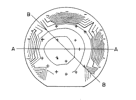
図4(A)に示す実施例1のシャワーヘッド部は、半径Rが99mm(直径198mm)の位置に、直径L2が1.3mmの略リング状に大口径ガス噴射孔80Aを設け(オリエンテーションフラット部分は直線状に設ける)、他の略格子状に配列された通常のガス噴射孔80の直径L1を1.1mmに設定した。また、最外周のガス噴射孔80の直径は230mmである。
図4(B)に示す実施例2のシャワーヘッド部は、半径Rが99mm(直径198mm)の位置に、直径L2が1.5mmの大口径ガス噴射孔80Aを設け、他の通常のガス噴射孔80の直径L1を上記と同じ1.1mmに設定した。また、最外周のガス噴射孔80の直径は230mmである。
【0028】
図4(C)に示す実施例3のシャワーヘッド部は、半径Rが99mm(直径198mm)の位置に、直径L2が1.7mmの大口径ガス噴射孔80Aを設け、他の通常のガス噴射孔80の直径L1を上記と同じ1.1mmに設定した。また、最外周のガス噴射孔80の直径は230mmである。
図4(D)に示す比較例1のシャワーヘッド部は、従来使用されていたものであり、直径L1が1.1mmの通常のガス噴射孔80を略格子状に均一に分散させて設けてあり、大口径ガス噴射孔は設けていない。また、最外周のガス噴射孔80の直径は230mmである。
【0029】
図4(E)に示す比較例2のシャワーヘッド部は、直径L1を上記比較例1よりも小さい0.8mmの通常のガス噴射孔80を略格子状に均一に分散させて設けてあり、大口径ガス噴射孔は設けていない。また、最外周のガス噴射孔80の直径は230mmである。
図4(F)に示す比較例3のシャワーヘッド部は、半径Rが100mm(直径200mm)の位置に、直径L2が2.0mmの大口径ガス噴射孔80Aを設け、その内側のみに直径L1を前述した各実施例と同じ1.1mmに設定した通常のガス噴射孔80を設けた。
尚、ウエハ及びシャワーヘッド間の距離は全て17mmに設定した。核成長成膜操作と本成膜操作を行なった時の成膜条件は表2に示されており、Arガスをキャリアガスとして用い、N2 ガスを希釈ガスとして用いている。これらの成膜条件は、共に供給律速となる成膜条件である。
【0030】
【表2】
図5は各実施例及び比較例のウエハ各部におけるシート抵抗(膜厚に反比例)を示しており、先の表1は、この測定結果をまとめたものである。図5にも示すように実施例1〜3の測定値は、ウエハ周縁部の値を含めてもそれ程大きな変動はなく、シート抵抗(膜厚)が略均一であることが判る。
具体的には、この図5に示す値をまとめた前記表1から明らかなように、本発明の実施例1〜3においては、核成長成膜操作の膜厚均一性は4.43以下であり、また、本成膜操作の膜厚均一性は5.16%以下であり、共に成膜速度は僅かに低下するが、膜厚均一性を大幅に向上させることができる。特に、実施例2及び3の場合には、膜厚の支配的要因となる本成膜操作における膜厚均一性はそれぞれ3.94%及び4.27%となって非常に優れており、実施例2の場合には最も好ましいことが判明する。
【0032】
これに対して、比較例1に示すような従来用いていたシャワーヘッド部の場合には、本成膜操作及び核成長成膜操作における膜厚均一性がそれぞれ5.25%及び11.18%であり、劣っている。そして、比較例2、3の場合には、核成長成膜操作における膜厚均一性は、比較例1よりも向上しているが、本成膜操作における膜厚均一性はそれぞれ6.98%及び9.27%となって比較例1よりもかなり劣っている。特に注意されたい点は、比較例3に示すように大口径ガス噴射孔を設けているが、その設置位置及び直径が本実施例1〜3の場合とは僅かに1mm程度だけ異なり、更に大口径ガス噴射孔80Aの外周に通常のガス噴射孔を設けない場合には、膜厚均一性が低下している点である。すなわち、大口径ガス噴射孔80Aの設定値及びこの直径等が非常に大きな要因となっている。
【0033】
これにより、大口径ガス噴射孔80Aを、クランプリングの内周端の上方に位置精度良く、且つ孔径もそれ程大きくすることなく設けることにより、核成長成膜操作及び本成膜操作において共に膜厚の均一性を向上できることが判明する。ここで、大口径ガス噴射孔80Aの設置位置についてのより詳しい評価を行なったので、それについて説明する。
図6は大口径ガス噴射孔の位置を評価するためのウエハ表面上における膜厚の等高線を示し、図7は図6中のA−A線及びB−B線方向におけるシート抵抗(膜厚に反比例)を示すグラフである。
【0034】
ここでは比較例3に用いたシャワーヘッド部に類似したシャワーヘッド部を用い、大口径ガス噴射孔80Aの直径を2mmとし、このガス噴射孔80Aまでの半径RをA−A線方向では99.2mmとし、B−B線方向では103mmとして設定し、成膜を行なった。尚、大口径ガス噴射孔80Aの外周には、通常のガス噴射孔を設けていない。
この場合、図7から明らかなように大口径ガス噴射孔80Aの設定位置を、僅か3.8mm(=103mm−99.2mm)だけ移動しただけで、ウエハ周辺部における膜厚は、極端に変動しており、これからも大口径ガス噴射孔80Aの設置位置は、膜厚均一性の改善の上から非常に重要であることが判明する。尚、図6中における太い実線は膜厚の平均値の等高線を示し、+は平均値より膜厚が厚い部分を示し、−は平均値より膜厚が薄い部分を示している。
【0035】
上記実施例では、シャワーヘッド部74における単位面積当たりのガス噴射量を多くする構成として、他の部分のガス噴射孔80よりも直径の大きな大口径ガス噴射孔80Aを設けるようにしたが、これに限定されず、例えば図8に示すように単位面積当たりのガス噴射量を多くすべき部分のガス噴射孔80Bの密度を高くして、結果的に単位面積当たりのガス噴射量を多くするようにしてもよく、この場合にも前述したと同様な作用効果を得ることができる。この場合、形成密度を上げたこのガス噴射孔80Bの直径と、この周辺のガス噴射孔80の直径は同じであり、同一ドリルで穿孔加工を行なうことができる。
【0036】
尚、上記実施例にあっては、タングステン膜を成膜する場合を例にとって説明したが、他の材料の成膜、例えばWSi、Ti、TiN、TiSi、Si、SiO2 等の成膜にも適用し得るのは勿論である。また、熱処理装置の加熱部としては、ランプ加熱に限定されず、抵抗加熱を用いてもよい。更に、ウエハガスも8インチのものに限定されず、6インチ、12インチ或いはそれ以上のウエハサイズにも適用し得るのは勿論である。
【0037】
【発明の効果】
以上説明したように、本発明の熱処理装置によれば、次のように優れた作用効果を発揮することができる。
被処理体の平面よりも大きい範囲に亘ってガス噴射孔を設け、被処理体押さえ部材に対向する部分の一部、特に、被処理体押さえ部材の内周端に対応する部分の単位面積当たりのガス噴射量を他の部分よりも多くするようにしたので、膜厚が大きくなる傾向にある被処理体中央部の成膜量を抑制し、膜厚が小さくなる傾向にある成膜量を促進することができるので、全体としての膜厚の均一性を大幅に向上させることができる。
特に、処理ガスの濃度分布が成膜速度に対して支配的な要因となる供給律速条件下における膜厚の均一性をより向上させることができる。
【図面の簡単な説明】
【図1】本発明に係る熱処理装置の一実施例を示す断面図である。
【図2】図1に示す装置のシャワーヘッド部と載置台の部分を示す拡大断面図である。
【図3】シャワーヘッド部を示す平面図である。
【図4】本発明装置の膜厚均一性を評価するために形成された複数のシャワーヘッド部を示す模式図である。
【図5】各実施例及び比較例のウエハ各部におけるシート抵抗(膜厚に反比例)を示すグラフである。
【図6】大口径ガス噴射孔の位置を評価するためのウエハ表面上における膜厚の等高線を示す図である。
【図7】図6中のA−A線及びB−B線方向におけるシート抵抗(膜厚に反比例)を示すグラフである。
【図8】本発明装置のシャワーヘッド部の変形例を示す平面図である。
【図9】一般的な熱処理装置を示す構成図である。
【符号の説明】
14 成膜処理装置(熱処理装置)
16 処理容器
22 載置台
36 被処理体押さえ部材
38 クランプリング
38A 内周端
44 透過窓
48 加熱ランプ(加熱部)
74 シャワーヘッド部
76 ヘッド本体
80 ガス噴射孔
80A 大口径ガス噴射孔
W 半導体ウエハ(被処理体)[0001]
BACKGROUND OF THE INVENTION
The present invention relates to a heat treatment apparatus for forming, for example, a metal thin film, a silicon oxide film, a silicon film, and the like.
[0002]
[Prior art]
In general, in the manufacturing process of a semiconductor integrated circuit, W (tungsten), WSi (tungsten silicide), Ti (in order to form a wiring pattern on the surface of a semiconductor wafer, which is an object to be processed, or to fill a recess such as between wirings. Thin films are formed by depositing metals or metal compounds such as titanium), TiN (titanium nitride), and TiSi (titanium silicide).
[0003]
There are three methods for forming this type of metal thin film, such as H2 (Hydrogen) reduction method, SiHFour (Silane) reduction method, SiH2 Cl2 (Dichlorosilane) reduction method is known, SiH2 Cl2 The reduction method is a method of forming a W or WSi (tungsten silicide) film at a high temperature of about 600 ° C. using, for example, dichlorosilane as a reducing gas in order to form a wiring pattern.Four The reduction method is a method of forming a W or WSi film at a low temperature of about 450 ° C., which is lower than the previous method, using, for example, silane as a reducing gas in order to form a wiring pattern.
[0004]
H2 The reduction method is a method of depositing a W film at a temperature of about 400 to 430 ° C. using, for example, hydrogen as a reducing gas in order to fill a hole on the wafer surface such as a recess between wirings.
In any of the above cases, for example, WF6(Tungsten hexafluoride) is used. A general heat treatment apparatus for forming such a metal thin film is shown in FIG. 9, and is formed, for example, with a thin carbon material or an aluminum compound in a
[0005]
And the heat ray from the heating means 8 permeate | transmits the permeation | transmission window 6, reaches the mounting base 4, heats this, and heats and maintains the semiconductor wafer W arrange | positioned on it at predetermined temperature indirectly. At the same time, the process gas from the
[0006]
[Problems to be solved by the invention]
By the way, in the film-forming process with respect to a semiconductor wafer, the in-plane uniformity of a film thickness must be maintained highly from a viewpoint of the improvement of the electrical characteristics and yield of a device. In the apparatus configuration as described above, the processing gas injected from the
[0007]
In particular, the above-mentioned film thickness uniformity does not decrease so much under the reaction-controlled conditions where the film formation rate mainly depends on the process temperature, but under the supply-controlled conditions where the film formation rate mainly depends on the gas concentration. However, there is a problem that the film thickness at the center of the wafer is larger than that at the peripheral edge and the film thickness uniformity is greatly reduced. For this reason, various distributions have been made to the flow rate of the processing gas supplied from the shower head, but the relationship between the gas flow rate and the film thickness is very delicate, and the optimum one has not been obtained. Currently.
The present invention has been devised to pay attention to the above problems and to effectively solve them. The objective of this invention is providing the heat processing apparatus which can improve the in-plane uniformity of a film thickness by giving the shower head part an appropriate distribution of the gas supply amount.
[0008]
[Means for Solving the Problems]
In order to solve the above problems, the present invention provides a processing container having a mounting table on which a target object is mounted, and a peripheral portion of the target object to be pressed to move the target object to the mounting table side. To-be-treated object pressing member provided so as to be able to move up and down, a heating unit for heating the to-be-treated object, and a shower provided to face the mounting table and having a plurality of gas injection holes formed on the lower surface In the heat treatment apparatus having a head part, the gas injection holes of the shower head part are provided over a range larger than the plane of the object to be processed,About the lower surface of the shower head part,Except for the part facing the object pressing member, the inside thereof is set so that the gas injection amount per unit area is substantially uniform, and a part of the part facing the object pressing member is a unit. The gas injection amount per area is set to be larger than the gas injection amount.
[0009]
Thereby, the gas injection amount per unit area from the shower head portion is substantially the same on the inner side and the outer side of the portion corresponding to the outer peripheral end of the processing object pressing member. In addition, since the gas injection amount per unit area of the portion corresponding to the processing object pressing member is set to be large, this suppresses film formation in the central portion of the processing object, and makes the film thickness uniform as a whole. Can be improved.
[0010]
In this case, in order to increase the gas injection amount per unit area, the diameter of the gas injection hole in the corresponding part is made larger than the diameter of the gas injection hole in the other part, or the diameter of the gas injection hole is the entire surface. In other words, the density of the corresponding gas injection holes may be increased by setting the same.
In addition, when the object pressing member has a certain width, it is preferable to provide the gas injection hole having a large diameter at a portion corresponding to the inner peripheral end of the object pressing member in order to improve the film thickness uniformity. Most preferable from the viewpoint.
[0011]
DETAILED DESCRIPTION OF THE INVENTION
Hereinafter, an embodiment of a heat treatment apparatus according to the present invention will be described in detail with reference to the accompanying drawings. 1 is a cross-sectional view showing an embodiment of a heat treatment apparatus according to the present invention, FIG. 2 is an enlarged cross-sectional view showing a shower head portion and a mounting table portion of the apparatus shown in FIG. 1, and FIG. 3 is a plan view showing the shower head portion. FIG.
[0012]
In this embodiment, a film forming apparatus will be described as an example of the heat treatment apparatus. The film forming apparatus 14 includes a processing container 16 formed into a cylindrical shape or a box shape by using aluminum or the like, for example, and a cylindrical reflector standing from the bottom of the processing container is provided in the processing container 16. On 18, for example, a mounting table 22 for mounting a semiconductor wafer W as an object to be processed is provided via a holding member 20 having an L-shaped cross section. The support column 18 and the holding member 20 are made of a heat ray transmissive material, such as quartz, and the mounting table 22 is made of, for example, a carbon material having a thickness of about 1 mm, an aluminum compound such as AlN, or the like. .
Below the mounting table 22, a plurality of, for example, three
[0013]
The lower end of the push-
[0014]
In addition, a
The side wall of the
[0015]
Further, on the outer peripheral side of the mounting table 22, a ring-shaped rectifying plate 62 having a large number of rectifying holes 60 is provided by being supported by a
[0016]
On the other hand, a
The gas introduction port 78 has a gas necessary for processing via a gas passage, for example, WF.6, Ar, SiHFour, H2 , N2 Etc. are connected so that the flow rate can be controlled.
A large number of gas injection holes 80 for releasing the gas supplied into the head
[0017]
Here, as shown in FIGS. 2 and 3, the
Specifically, the gas injection holes 80 are arranged in a substantially lattice shape over a range larger than the wafer area, and the diameter L2 of the
[0018]
Further, the wafer W is provided with an orientation flat formed by cutting a part of the periphery of the wafer in a straight line, a notch formed by cutting a semicircle with a diameter of several millimeters, etc. as a notch for positioning. The large-diameter gas injection holes 80A are arranged corresponding to the contour of the wafer W. In FIG. 3, the four large-diameter gas injection holes 80Aa on the right side correspond to the orientation flat of the wafer. In the illustrated example, the diameter of the large-diameter
[0019]
In the illustrated example, the large-diameter gas injection holes 80A are arranged in one row, but they may be arranged in a plurality of examples of two rows or more.
Further, the thickness W1 of the
[0020]
Next, the operation of the present embodiment configured as described above will be described.
First, when performing a film formation process of a metal film such as tungsten on the wafer surface, the
[0021]
Next, WF as a processing gas from a processing gas source (not shown)6, SiHFour, H2 And the like are supplied to the
[0022]
The radiated heat rays pass through the
[0023]
Here, in the present embodiment, with respect to the gas injection holes 80 and 80A of the
[0024]
In this case, it is preferable from the viewpoint of improving the film thickness uniformity to provide the normal gas injection holes 80 over a certain range, for example, about several centimeters, outside the large-diameter gas injection holes 80A. This is because in order to improve the film thickness uniformity in the wafer surface, it is necessary to form a certain amount of film on the upper surface of the
In addition, in actual film forming operations, for example, a tungsten film is generally formed on an underlying TiN film. The film formation of the tungsten film is performed in the main film forming operation and in the main film forming operation. In order to eliminate the selectivity, there is a nuclear growth film forming operation that is performed only for a short time prior to the main film forming operation. Both can improve the in-plane uniformity of film thickness.
[0025]
Next, since the in-plane uniformity of film formation was evaluated for various showerhead structures, the explanation will be given.
In the evaluation, a wafer having a diameter of 8 inches (diameter 20 cm) was used and pressed and held by the clamp ring so that the overlapping width W3 (see FIG. 2) of the peripheral edge of the wafer was about 1 mm. As a result, the diameter (see FIG. 2) between the inner peripheral ends 38A of the
Six types of showerhead structures were prepared as schematically shown in FIG. The structure and evaluation results are shown in Table 1 and FIG. 4A to 4C show Examples 1 to 3, respectively, and FIGS. 4D to 4F show Comparative Examples 1 to 3, respectively.
[0026]
[Table 1]
The shower head portion of Example 1 shown in FIG. 4A is provided with a large-diameter
The shower head unit of Example 2 shown in FIG. 4B is provided with a large-diameter
[0028]
The shower head portion of Example 3 shown in FIG. 4C is provided with a large-diameter
The shower head portion of Comparative Example 1 shown in FIG. 4 (D) has been used in the past, and normal gas injection holes 80 having a diameter L1 of 1.1 mm are uniformly distributed in a substantially lattice shape. There is no large-diameter gas injection hole. The diameter of the outermost
[0029]
The shower head portion of Comparative Example 2 shown in FIG. 4 (E) is provided with regular gas injection holes 80 having a diameter L1 smaller than that of Comparative Example 1 of 0.8 mm, which are uniformly dispersed in a substantially lattice shape. No large-diameter gas injection hole is provided. The diameter of the outermost
In the shower head portion of Comparative Example 3 shown in FIG. 4 (F), a large-diameter
The distance between the wafer and the shower head was set to 17 mm. The film formation conditions when the nuclear growth film formation operation and the main film formation operation are performed are shown in Table 2. Ar gas is used as a carrier gas, and N2 Gas is used as the dilution gas. These film forming conditions are film forming conditions that are both rate-controlled.
[0030]
[Table 2]
FIG. 5 shows the sheet resistance (in inverse proportion to the film thickness) in each part of the wafer of each example and comparative example. Table 1 above summarizes the measurement results. As shown in FIG. 5, it can be seen that the measured values of Examples 1 to 3 do not vary so much even if the value of the wafer peripheral portion is included, and the sheet resistance (film thickness) is substantially uniform.
Specifically, as is clear from Table 1 that summarizes the values shown in FIG. 5, in Examples 1 to 3 of the present invention, the film thickness uniformity of the nuclear growth film forming operation is 4.43 or less. In addition, the film thickness uniformity of this film forming operation is 5.16% or less, and the film forming speed is slightly reduced in both cases, but the film thickness uniformity can be greatly improved. In particular, in the case of Examples 2 and 3, the film thickness uniformity in the present film forming operation, which is a dominant factor of the film thickness, is 3.94% and 4.27%, respectively, which are very excellent. In the case of Example 2, it turns out to be most preferable.
[0032]
On the other hand, in the case of the conventionally used shower head as shown in Comparative Example 1, the film thickness uniformity in the present film formation operation and the nucleus growth film formation operation is 5.25% and 11.18%, respectively. And inferior. In Comparative Examples 2 and 3, the film thickness uniformity in the nucleus growth film forming operation is improved as compared with Comparative Example 1, but the film thickness uniformity in the film forming operation is 6.98%. And 9.27%, which is considerably inferior to Comparative Example 1. The point to be particularly noted is that a large-diameter gas injection hole is provided as shown in Comparative Example 3, but its installation position and diameter are slightly different from those in Examples 1 to 3 by about 1 mm, which is even larger. In the case where normal gas injection holes are not provided on the outer periphery of the diameter
[0033]
Accordingly, by providing the large-diameter
6 shows the contour lines of the film thickness on the wafer surface for evaluating the position of the large-diameter gas injection hole, and FIG. 7 shows the sheet resistance (in the film thickness in the AA line and BB line directions in FIG. It is a graph which shows (inverse proportion).
[0034]
Here, a shower head portion similar to the shower head portion used in Comparative Example 3 is used, the diameter of the large-diameter
In this case, as apparent from FIG. 7, the film thickness at the wafer peripheral portion fluctuates extremely only by moving the setting position of the large-diameter
[0035]
In the above embodiment, the large-diameter
[0036]
In the above embodiment, the case where a tungsten film is formed has been described as an example. However, other materials such as WSi, Ti, TiN, TiSi, Si, and SiO are formed.2 Needless to say, the present invention can also be applied to film formation. Further, the heating unit of the heat treatment apparatus is not limited to lamp heating, and resistance heating may be used. Further, the wafer gas is not limited to 8 inches, and it is of course applicable to wafer sizes of 6 inches, 12 inches or more.
[0037]
【The invention's effect】
As described above, according to the heat treatment apparatus of the present invention, the following excellent effects can be achieved.
A gas injection hole is provided over a range larger than the plane of the object to be processed, and a part of the part facing the object pressing member, particularly a unit area of the part corresponding to the inner peripheral end of the object pressing member. Since the gas injection amount is increased more than other portions, the film formation amount in the central part of the object to be processed, which tends to increase the film thickness, is suppressed, and the film formation amount, which tends to decrease the film thickness, is reduced. Since it can promote, the uniformity of the film thickness as a whole can be improved significantly.
In particular, it is possible to further improve the film thickness uniformity under a supply rate-limiting condition in which the concentration distribution of the processing gas is a dominant factor with respect to the film formation rate.
[Brief description of the drawings]
FIG. 1 is a cross-sectional view showing an embodiment of a heat treatment apparatus according to the present invention.
2 is an enlarged cross-sectional view showing a shower head portion and a mounting table portion of the apparatus shown in FIG. 1;
FIG. 3 is a plan view showing a shower head unit.
FIG. 4 is a schematic view showing a plurality of shower head portions formed in order to evaluate the film thickness uniformity of the apparatus of the present invention.
FIG. 5 is a graph showing sheet resistance (in inverse proportion to film thickness) in each part of the wafer in each example and comparative example.
FIG. 6 is a diagram showing contour lines of film thickness on a wafer surface for evaluating the position of a large-diameter gas injection hole.
7 is a graph showing sheet resistance (in inverse proportion to the film thickness) in the direction of the lines AA and BB in FIG. 6;
FIG. 8 is a plan view showing a modification of the shower head portion of the device of the present invention.
FIG. 9 is a configuration diagram showing a general heat treatment apparatus.
[Explanation of symbols]
14 Deposition processing equipment (heat treatment equipment)
16 Processing container
22 Mounting table
36 Workpiece holding member
38 Clamp ring
38A Inner edge
44 Transmission window
48 Heating lamp (heating unit)
74 Shower head
76 Head body
80 Gas injection hole
80A large-diameter gas injection hole
W Semiconductor wafer (object to be processed)
Claims (6)
前記シャワーヘッド部のガス噴射孔は、前記被処理体の平面よりも大きい範囲に亘って設けられ、前記シャワーヘッド部の下面については、前記被処理体押さえ部材に対向する部分を除いてその内側は、単位面積当たりのガス噴射量が略均一となるように設定され、前記被処理体押さえ部材に対向する部分の一部は、単位面積当たりのガス噴射量が前記ガス噴射量よりも多くなるように設定されることを特徴とする熱処理装置。A processing container having a mounting table for mounting the processing object therein, and a processing object provided so as to be movable up and down in order to fix the processing object to the mounting table side by pressing a peripheral edge of the processing object. In a heat treatment apparatus having a pressing member, a heating unit that heats the object to be processed, and a shower head unit that is provided to face the mounting table and in which a large number of gas injection holes are formed on the lower surface.
The gas injection holes of the shower head unit are provided over a range larger than the plane of the object to be processed, and the lower surface of the shower head part is located on the inner side except for the part facing the object to be processed pressing member. Is set so that the gas injection amount per unit area is substantially uniform, and the gas injection amount per unit area is larger than the gas injection amount in a part of the portion facing the object pressing member. The heat processing apparatus characterized by setting as follows.
前記シャワーヘッド部のガス噴射孔は、前記被処理体の平面よりも大きい範囲に亘って設けられ、前記被処理体押さえ部材に対向する部分を除いてその内側は、単位面積当たりのガス噴射量が略均一となるように設定されると共に、前記被処理体押さえ部材に対向する部分の一部のガス噴射孔の直径は、前記被処理体押さえ部材に対向する部分よりも内側に位置するガス噴射孔の直径よりも大きく設定されて、前記被処理体押さえ部材に対向する部分の一部は、単位面積当たりのガス噴射量が前記ガス噴射量よりも多くなるように設定されることを特徴とする熱処理装置。A processing container having a mounting table for mounting the processing object therein, and a processing object provided so as to be movable up and down in order to fix the processing object to the mounting table side by pressing the peripheral edge of the processing object. In a heat treatment apparatus having a pressing member, a heating unit that heats the object to be processed, and a shower head unit that is provided to face the mounting table and has a plurality of gas injection holes formed on the lower surface thereof,
The gas injection holes of the shower head section are provided over a range larger than the plane of the object to be processed, and the inside thereof except for the portion facing the object to be processed pressing member is the gas injection amount per unit area. Is set so as to be substantially uniform, and the diameter of a part of the gas injection holes in the portion facing the object pressing member is located inside the portion facing the object pressing member. A part of the portion that is set larger than the diameter of the injection hole and faces the object pressing member is set such that the gas injection amount per unit area is larger than the gas injection amount. Heat treatment equipment.
前記シャワーヘッド部のガス噴射孔は、前記被処理体の平面よりも大きい範囲に亘って設けられ、前記被処理体押さえ部材に対向する部分を除いてその内側は、単位面積当たりのガス噴射量が略均一となるように設定されると共に、前記被処理体押さえ部材に対向する部分の一部のガス噴射孔の密度は、前記被処理体押さえ部材に対向する部分よりも内側に位置するガス噴射孔の密度よりも大きく設定されて、前記被処理体押さえ部材に対向する部分の一部は、単位面積当たりのガス噴射量が前記ガス噴射量よりも多くなるように設定されることを特徴とする熱処理装置。A processing container having a mounting table for mounting the processing object therein, and a processing object provided so as to be movable up and down in order to fix the processing object to the mounting table side by pressing the peripheral edge of the processing object. In a heat treatment apparatus having a pressing member, a heating unit that heats the object to be processed, and a shower head unit that is provided to face the mounting table and has a plurality of gas injection holes formed on the lower surface thereof,
The gas injection holes of the shower head section are provided over a range larger than the plane of the object to be processed, and the inside thereof except for the portion facing the object to be processed pressing member is the gas injection amount per unit area. gas but is set to be substantially uniform Rutotomoni, the density of a part of the gas injection hole of the portion facing the workpiece holding member is located inside the portion facing the object to be processed pressing member A part of the portion that is set larger than the density of the injection holes and faces the object pressing member is set such that the gas injection amount per unit area is larger than the gas injection amount. Heat treatment equipment.
Priority Applications (6)
| Application Number | Priority Date | Filing Date | Title |
|---|---|---|---|
| JP07317798A JP4147608B2 (en) | 1998-03-06 | 1998-03-06 | Heat treatment equipment |
| EP99937952A EP1061155B1 (en) | 1998-03-06 | 1999-03-05 | Vacuum processing apparatus |
| DE69927003T DE69927003T2 (en) | 1998-03-06 | 1999-03-05 | VACUUM TREATMENT DEVICE |
| KR10-2000-7009817A KR100514726B1 (en) | 1998-03-06 | 1999-03-05 | Vacuum processing apparatus |
| US09/623,574 US6599367B1 (en) | 1998-03-06 | 1999-03-05 | Vacuum processing apparatus |
| PCT/JP1999/001078 WO1999045166A1 (en) | 1998-03-06 | 1999-03-05 | Vacuum processing apparatus |
Applications Claiming Priority (1)
| Application Number | Priority Date | Filing Date | Title |
|---|---|---|---|
| JP07317798A JP4147608B2 (en) | 1998-03-06 | 1998-03-06 | Heat treatment equipment |
Publications (2)
| Publication Number | Publication Date |
|---|---|
| JPH11256328A JPH11256328A (en) | 1999-09-21 |
| JP4147608B2 true JP4147608B2 (en) | 2008-09-10 |
Family
ID=13510608
Family Applications (1)
| Application Number | Title | Priority Date | Filing Date |
|---|---|---|---|
| JP07317798A Expired - Fee Related JP4147608B2 (en) | 1998-03-06 | 1998-03-06 | Heat treatment equipment |
Country Status (6)
| Country | Link |
|---|---|
| US (1) | US6599367B1 (en) |
| EP (1) | EP1061155B1 (en) |
| JP (1) | JP4147608B2 (en) |
| KR (1) | KR100514726B1 (en) |
| DE (1) | DE69927003T2 (en) |
| WO (1) | WO1999045166A1 (en) |
Families Citing this family (47)
| Publication number | Priority date | Publication date | Assignee | Title |
|---|---|---|---|---|
| JP4147608B2 (en) * | 1998-03-06 | 2008-09-10 | 東京エレクトロン株式会社 | Heat treatment equipment |
| US8048806B2 (en) | 2000-03-17 | 2011-11-01 | Applied Materials, Inc. | Methods to avoid unstable plasma states during a process transition |
| US7196283B2 (en) | 2000-03-17 | 2007-03-27 | Applied Materials, Inc. | Plasma reactor overhead source power electrode with low arcing tendency, cylindrical gas outlets and shaped surface |
| US20040129218A1 (en) * | 2001-12-07 | 2004-07-08 | Toshiki Takahashi | Exhaust ring mechanism and plasma processing apparatus using the same |
| US20040025791A1 (en) * | 2002-08-09 | 2004-02-12 | Applied Materials, Inc. | Etch chamber with dual frequency biasing sources and a single frequency plasma generating source |
| US20040031565A1 (en) * | 2002-08-13 | 2004-02-19 | Taiwan Semiconductor Manufacturing Co., Ltd. | Gas distribution plate for processing chamber |
| US7186630B2 (en) | 2002-08-14 | 2007-03-06 | Asm America, Inc. | Deposition of amorphous silicon-containing films |
| WO2004038777A1 (en) * | 2002-10-24 | 2004-05-06 | Tokyo Electron Limited | Heat treatment apparatus |
| US6942753B2 (en) * | 2003-04-16 | 2005-09-13 | Applied Materials, Inc. | Gas distribution plate assembly for large area plasma enhanced chemical vapor deposition |
| US8580076B2 (en) * | 2003-05-22 | 2013-11-12 | Lam Research Corporation | Plasma apparatus, gas distribution assembly for a plasma apparatus and processes therewith |
| US20040235299A1 (en) * | 2003-05-22 | 2004-11-25 | Axcelis Technologies, Inc. | Plasma ashing apparatus and endpoint detection process |
| US20070248515A1 (en) * | 2003-12-01 | 2007-10-25 | Tompa Gary S | System and Method for Forming Multi-Component Films |
| WO2005067022A1 (en) * | 2003-12-26 | 2005-07-21 | Tadahiro Ohmi | Shower plate, plasma processing system, and process for producing product |
| US8083853B2 (en) * | 2004-05-12 | 2011-12-27 | Applied Materials, Inc. | Plasma uniformity control by gas diffuser hole design |
| US8328939B2 (en) * | 2004-05-12 | 2012-12-11 | Applied Materials, Inc. | Diffuser plate with slit valve compensation |
| US8074599B2 (en) * | 2004-05-12 | 2011-12-13 | Applied Materials, Inc. | Plasma uniformity control by gas diffuser curvature |
| US7429410B2 (en) * | 2004-09-20 | 2008-09-30 | Applied Materials, Inc. | Diffuser gravity support |
| KR100634451B1 (en) * | 2005-01-10 | 2006-10-16 | 삼성전자주식회사 | Apparatus for manufacturing semiconductor device |
| US7198677B2 (en) * | 2005-03-09 | 2007-04-03 | Wafermasters, Inc. | Low temperature wafer backside cleaning |
| US7695633B2 (en) * | 2005-10-18 | 2010-04-13 | Applied Materials, Inc. | Independent control of ion density, ion energy distribution and ion dissociation in a plasma reactor |
| US7727413B2 (en) * | 2006-04-24 | 2010-06-01 | Applied Materials, Inc. | Dual plasma source process using a variable frequency capacitively coupled source to control plasma ion density |
| US20070246162A1 (en) * | 2006-04-24 | 2007-10-25 | Applied Materials, Inc. | Plasma reactor apparatus with an inductive plasma source and a VHF capacitively coupled plasma source with variable frequency |
| US20070246163A1 (en) * | 2006-04-24 | 2007-10-25 | Applied Materials, Inc. | Plasma reactor apparatus with independent capacitive and inductive plasma sources |
| US20070245961A1 (en) * | 2006-04-24 | 2007-10-25 | Applied Materials, Inc. | Dual plasma source process using a variable frequency capacitively coupled source for controlling plasma ion dissociation |
| US7780864B2 (en) * | 2006-04-24 | 2010-08-24 | Applied Materials, Inc. | Process using combined capacitively and inductively coupled plasma sources for controlling plasma ion radial distribution |
| US7645357B2 (en) * | 2006-04-24 | 2010-01-12 | Applied Materials, Inc. | Plasma reactor apparatus with a VHF capacitively coupled plasma source of variable frequency |
| US20070245958A1 (en) * | 2006-04-24 | 2007-10-25 | Applied Materials, Inc. | Dual plasma source process using a variable frequency capacitively coupled source for controlling ion radial distribution |
| US20070246443A1 (en) * | 2006-04-24 | 2007-10-25 | Applied Materials, Inc. | Process using combined capacitively and inductively coupled plasma process for controlling plasma ion dissociation |
| US20070245960A1 (en) * | 2006-04-24 | 2007-10-25 | Applied Materials, Inc. | Process using combined capacitively and inductively coupled plasma sources for controlling plasma ion density |
| US20070246161A1 (en) * | 2006-04-24 | 2007-10-25 | Applied Materials, Inc. | Plasma reactor apparatus with a toroidal plasma source and a VHF capacitively coupled plasma source with variable frequency |
| KR100841741B1 (en) * | 2007-04-04 | 2008-06-27 | 주식회사 싸이맥스 | Vacuum processing equipment |
| US7976631B2 (en) | 2007-10-16 | 2011-07-12 | Applied Materials, Inc. | Multi-gas straight channel showerhead |
| US8342712B2 (en) | 2008-09-30 | 2013-01-01 | Disney Enterprises, Inc. | Kinetic flame device |
| US9371973B2 (en) | 2010-06-28 | 2016-06-21 | Shenzhen Liown Electronics Company Ltd. | Electronic lighting device and method for manufacturing same |
| US9129778B2 (en) | 2011-03-18 | 2015-09-08 | Lam Research Corporation | Fluid distribution members and/or assemblies |
| KR101239109B1 (en) * | 2011-09-23 | 2013-03-06 | 주성엔지니어링(주) | Chamber for Uniform Film Deposition |
| US20140273460A1 (en) * | 2013-03-13 | 2014-09-18 | Applied Materials, Inc. | Passive control for through silicon via tilt in icp chamber |
| CN103305812A (en) * | 2013-06-08 | 2013-09-18 | 上海和辉光电有限公司 | Top electrode device |
| CN104103561B (en) * | 2014-07-24 | 2016-08-24 | 河北神通光电科技有限公司 | Etching cavity and etching system thereof for gaseous hydrogen fluoride etching silicon dioxide |
| US10760161B2 (en) * | 2014-09-05 | 2020-09-01 | Applied Materials, Inc. | Inject insert for EPI chamber |
| US20170081757A1 (en) * | 2015-09-23 | 2017-03-23 | Applied Materials, Inc. | Shadow frame with non-uniform gas flow clearance for improved cleaning |
| KR102470206B1 (en) * | 2017-10-13 | 2022-11-23 | 삼성디스플레이 주식회사 | Manufacturing method for metal oxide and display device comprising the metal oxide |
| KR102477354B1 (en) * | 2018-03-29 | 2022-12-15 | 삼성전자주식회사 | Plasma processing apparatus including gas distribution plate |
| KR102827753B1 (en) * | 2020-04-07 | 2025-07-02 | 삼성디스플레이 주식회사 | Method for manufacturing a display apparatus |
| US12179223B2 (en) * | 2020-10-30 | 2024-12-31 | Kabushiki Kaisha Toshiba | Rectifying plate, fluid-introducing apparatus, and film-forming apparatus |
| JP7631170B2 (en) * | 2020-10-30 | 2025-02-18 | 株式会社東芝 | Flow plate, fluid introduction device, and film formation device |
| JP7629813B2 (en) * | 2021-07-06 | 2025-02-14 | 東京エレクトロン株式会社 | Plasma Processing Equipment |
Family Cites Families (14)
| Publication number | Priority date | Publication date | Assignee | Title |
|---|---|---|---|---|
| US4792378A (en) | 1987-12-15 | 1988-12-20 | Texas Instruments Incorporated | Gas dispersion disk for use in plasma enhanced chemical vapor deposition reactor |
| JPH02198138A (en) * | 1989-01-27 | 1990-08-06 | Nec Corp | Electrode plate of parallel plate type dry etching apparatus |
| JPH0344471A (en) * | 1989-07-12 | 1991-02-26 | Mitsubishi Electric Corp | Chemical vapor deposition device |
| EP0413239B1 (en) * | 1989-08-14 | 1996-01-10 | Applied Materials, Inc. | Gas distribution system and method of using said system |
| JPH04211115A (en) | 1990-01-26 | 1992-08-03 | Fujitsu Ltd | Rf plasma cvd apparatus and thin film forming method |
| JPH0661157A (en) * | 1992-08-12 | 1994-03-04 | Sharp Corp | Semiconductor manufacturing device |
| JPH06151368A (en) * | 1992-11-02 | 1994-05-31 | Nec Corp | Dry etching device |
| KR950020993A (en) * | 1993-12-22 | 1995-07-26 | 김광호 | Semiconductor manufacturing device |
| JP2726005B2 (en) * | 1994-07-20 | 1998-03-11 | 株式会社ジーティシー | Film forming apparatus and film forming method |
| JPH0930892A (en) | 1995-07-20 | 1997-02-04 | Yamaha Corp | Plasma cvd device |
| US5781693A (en) * | 1996-07-24 | 1998-07-14 | Applied Materials, Inc. | Gas introduction showerhead for an RTP chamber with upper and lower transparent plates and gas flow therebetween |
| US6090210A (en) * | 1996-07-24 | 2000-07-18 | Applied Materials, Inc. | Multi-zone gas flow control in a process chamber |
| US6079356A (en) * | 1997-12-02 | 2000-06-27 | Applied Materials, Inc. | Reactor optimized for chemical vapor deposition of titanium |
| JP4147608B2 (en) * | 1998-03-06 | 2008-09-10 | 東京エレクトロン株式会社 | Heat treatment equipment |
-
1998
- 1998-03-06 JP JP07317798A patent/JP4147608B2/en not_active Expired - Fee Related
-
1999
- 1999-03-05 EP EP99937952A patent/EP1061155B1/en not_active Expired - Lifetime
- 1999-03-05 WO PCT/JP1999/001078 patent/WO1999045166A1/en not_active Ceased
- 1999-03-05 DE DE69927003T patent/DE69927003T2/en not_active Expired - Fee Related
- 1999-03-05 US US09/623,574 patent/US6599367B1/en not_active Expired - Fee Related
- 1999-03-05 KR KR10-2000-7009817A patent/KR100514726B1/en not_active Expired - Fee Related
Also Published As
| Publication number | Publication date |
|---|---|
| DE69927003T2 (en) | 2006-06-22 |
| DE69927003D1 (en) | 2005-10-06 |
| EP1061155A4 (en) | 2004-07-07 |
| JPH11256328A (en) | 1999-09-21 |
| KR20010041619A (en) | 2001-05-25 |
| EP1061155A1 (en) | 2000-12-20 |
| KR100514726B1 (en) | 2005-09-13 |
| WO1999045166A1 (en) | 1999-09-10 |
| EP1061155B1 (en) | 2005-08-31 |
| US6599367B1 (en) | 2003-07-29 |
Similar Documents
| Publication | Publication Date | Title |
|---|---|---|
| JP4147608B2 (en) | Heat treatment equipment | |
| JP3362552B2 (en) | Film processing equipment | |
| JP4288767B2 (en) | Manufacturing method of semiconductor device | |
| US5500388A (en) | Heat treatment process for wafers | |
| JPWO2007018139A1 (en) | Semiconductor device manufacturing method and substrate processing apparatus | |
| JP2001168047A (en) | Heating equipment for semiconductor manufacturing | |
| JP2002155366A (en) | Method and device of leaf type heat treatment | |
| JP3636864B2 (en) | Processing device and stage device | |
| TW202121510A (en) | Method for forming RuSi film and substrate processing system | |
| JPH09237763A (en) | Single wafer type heat treatment equipment | |
| JP2001035797A (en) | Substrate processing equipment | |
| JPH11204443A (en) | Single wafer type heat treatment equipment | |
| US11211265B2 (en) | Heat treatment apparatus and heat treatment method | |
| US20030205192A1 (en) | Film forming method | |
| JP4157718B2 (en) | Silicon nitride film manufacturing method and silicon nitride film manufacturing apparatus | |
| JP4329171B2 (en) | Film forming method and film forming apparatus | |
| JP2009021533A (en) | Vapor growth apparatus and vapor growth method | |
| JP4804636B2 (en) | Deposition method | |
| JP3835376B2 (en) | Deposition processing equipment | |
| JP4401481B2 (en) | Deposition method | |
| JP4877687B2 (en) | Deposition method | |
| WO2003069020A1 (en) | System for processing substrate and method for processing substrate | |
| JP2004335825A (en) | Substrate processing equipment | |
| JP4401479B2 (en) | Gas processing method | |
| JP3099102B2 (en) | Heat treatment equipment |
Legal Events
| Date | Code | Title | Description |
|---|---|---|---|
| A621 | Written request for application examination |
Free format text: JAPANESE INTERMEDIATE CODE: A621 Effective date: 20040512 |
|
| A131 | Notification of reasons for refusal |
Free format text: JAPANESE INTERMEDIATE CODE: A131 Effective date: 20070814 |
|
| A521 | Request for written amendment filed |
Free format text: JAPANESE INTERMEDIATE CODE: A523 Effective date: 20071004 |
|
| TRDD | Decision of grant or rejection written | ||
| A01 | Written decision to grant a patent or to grant a registration (utility model) |
Free format text: JAPANESE INTERMEDIATE CODE: A01 Effective date: 20080603 |
|
| A01 | Written decision to grant a patent or to grant a registration (utility model) |
Free format text: JAPANESE INTERMEDIATE CODE: A01 |
|
| A61 | First payment of annual fees (during grant procedure) |
Free format text: JAPANESE INTERMEDIATE CODE: A61 Effective date: 20080616 |
|
| FPAY | Renewal fee payment (event date is renewal date of database) |
Free format text: PAYMENT UNTIL: 20110704 Year of fee payment: 3 |
|
| R150 | Certificate of patent or registration of utility model |
Free format text: JAPANESE INTERMEDIATE CODE: R150 |
|
| LAPS | Cancellation because of no payment of annual fees |