JP4141138B2 - Method for manufacturing semiconductor device - Google Patents
Method for manufacturing semiconductor device Download PDFInfo
- Publication number
- JP4141138B2 JP4141138B2 JP2001390708A JP2001390708A JP4141138B2 JP 4141138 B2 JP4141138 B2 JP 4141138B2 JP 2001390708 A JP2001390708 A JP 2001390708A JP 2001390708 A JP2001390708 A JP 2001390708A JP 4141138 B2 JP4141138 B2 JP 4141138B2
- Authority
- JP
- Japan
- Prior art keywords
- semiconductor
- region
- shape
- semiconductor region
- regions
- Prior art date
- Legal status (The legal status is an assumption and is not a legal conclusion. Google has not performed a legal analysis and makes no representation as to the accuracy of the status listed.)
- Expired - Fee Related
Links
- 239000004065 semiconductor Substances 0.000 title claims description 216
- 238000000034 method Methods 0.000 title claims description 51
- 238000004519 manufacturing process Methods 0.000 title claims description 21
- 239000013078 crystal Substances 0.000 claims description 138
- 238000002425 crystallisation Methods 0.000 claims description 55
- 230000008025 crystallization Effects 0.000 claims description 39
- 230000015572 biosynthetic process Effects 0.000 claims description 31
- 230000010355 oscillation Effects 0.000 claims description 31
- 230000001678 irradiating effect Effects 0.000 claims description 14
- 238000009826 distribution Methods 0.000 claims description 11
- 238000005530 etching Methods 0.000 claims description 10
- 239000010408 film Substances 0.000 description 122
- 239000010410 layer Substances 0.000 description 76
- 239000000758 substrate Substances 0.000 description 33
- 239000000463 material Substances 0.000 description 29
- 239000011521 glass Substances 0.000 description 20
- 229910021417 amorphous silicon Inorganic materials 0.000 description 16
- 230000003287 optical effect Effects 0.000 description 16
- 229910052581 Si3N4 Inorganic materials 0.000 description 15
- HQVNEWCFYHHQES-UHFFFAOYSA-N silicon nitride Chemical compound N12[Si]34N5[Si]62N3[Si]51N64 HQVNEWCFYHHQES-UHFFFAOYSA-N 0.000 description 15
- XUIMIQQOPSSXEZ-UHFFFAOYSA-N Silicon Chemical compound [Si] XUIMIQQOPSSXEZ-UHFFFAOYSA-N 0.000 description 13
- 238000010586 diagram Methods 0.000 description 13
- 229910052710 silicon Inorganic materials 0.000 description 13
- 239000010703 silicon Substances 0.000 description 13
- 229910021419 crystalline silicon Inorganic materials 0.000 description 11
- 238000010438 heat treatment Methods 0.000 description 11
- 230000008569 process Effects 0.000 description 11
- 230000000903 blocking effect Effects 0.000 description 10
- 230000003197 catalytic effect Effects 0.000 description 10
- PXHVJJICTQNCMI-UHFFFAOYSA-N nickel Substances [Ni] PXHVJJICTQNCMI-UHFFFAOYSA-N 0.000 description 10
- 239000007789 gas Substances 0.000 description 9
- 239000011347 resin Substances 0.000 description 9
- 229920005989 resin Polymers 0.000 description 9
- 238000004544 sputter deposition Methods 0.000 description 9
- 230000006911 nucleation Effects 0.000 description 8
- 238000010899 nucleation Methods 0.000 description 8
- 150000002894 organic compounds Chemical class 0.000 description 8
- 229910052782 aluminium Inorganic materials 0.000 description 7
- 230000004888 barrier function Effects 0.000 description 7
- 239000003054 catalyst Substances 0.000 description 7
- 230000006870 function Effects 0.000 description 7
- VYPSYNLAJGMNEJ-UHFFFAOYSA-N silicon dioxide Inorganic materials O=[Si]=O VYPSYNLAJGMNEJ-UHFFFAOYSA-N 0.000 description 7
- 238000004528 spin coating Methods 0.000 description 7
- 150000001340 alkali metals Chemical class 0.000 description 6
- 238000006243 chemical reaction Methods 0.000 description 6
- 230000005669 field effect Effects 0.000 description 6
- 238000005247 gettering Methods 0.000 description 6
- 239000012535 impurity Substances 0.000 description 6
- 238000013532 laser treatment Methods 0.000 description 6
- 230000001681 protective effect Effects 0.000 description 6
- 239000007787 solid Substances 0.000 description 6
- GYHNNYVSQQEPJS-UHFFFAOYSA-N Gallium Chemical compound [Ga] GYHNNYVSQQEPJS-UHFFFAOYSA-N 0.000 description 5
- 239000004642 Polyimide Substances 0.000 description 5
- 230000009471 action Effects 0.000 description 5
- 229910052783 alkali metal Inorganic materials 0.000 description 5
- XAGFODPZIPBFFR-UHFFFAOYSA-N aluminium Chemical compound [Al] XAGFODPZIPBFFR-UHFFFAOYSA-N 0.000 description 5
- 239000006185 dispersion Substances 0.000 description 5
- 230000000694 effects Effects 0.000 description 5
- 229910052733 gallium Inorganic materials 0.000 description 5
- 229920001721 polyimide Polymers 0.000 description 5
- 229910052814 silicon oxide Inorganic materials 0.000 description 5
- 229910052688 Gadolinium Inorganic materials 0.000 description 4
- UFHFLCQGNIYNRP-UHFFFAOYSA-N Hydrogen Chemical compound [H][H] UFHFLCQGNIYNRP-UHFFFAOYSA-N 0.000 description 4
- MQRWBMAEBQOWAF-UHFFFAOYSA-N acetic acid;nickel Chemical compound [Ni].CC(O)=O.CC(O)=O MQRWBMAEBQOWAF-UHFFFAOYSA-N 0.000 description 4
- 238000000137 annealing Methods 0.000 description 4
- 239000007864 aqueous solution Substances 0.000 description 4
- UIWYJDYFSGRHKR-UHFFFAOYSA-N gadolinium atom Chemical compound [Gd] UIWYJDYFSGRHKR-UHFFFAOYSA-N 0.000 description 4
- 239000002223 garnet Substances 0.000 description 4
- 239000001257 hydrogen Substances 0.000 description 4
- 229910052739 hydrogen Inorganic materials 0.000 description 4
- 239000011229 interlayer Substances 0.000 description 4
- 239000011777 magnesium Substances 0.000 description 4
- 229940078494 nickel acetate Drugs 0.000 description 4
- 238000007789 sealing Methods 0.000 description 4
- OKTJSMMVPCPJKN-UHFFFAOYSA-N Carbon Chemical compound [C] OKTJSMMVPCPJKN-UHFFFAOYSA-N 0.000 description 3
- 229910052779 Neodymium Inorganic materials 0.000 description 3
- 239000004840 adhesive resin Substances 0.000 description 3
- 229920006223 adhesive resin Polymers 0.000 description 3
- 239000002585 base Substances 0.000 description 3
- UMIVXZPTRXBADB-UHFFFAOYSA-N benzocyclobutene Chemical compound C1=CC=C2CCC2=C1 UMIVXZPTRXBADB-UHFFFAOYSA-N 0.000 description 3
- 239000004020 conductor Substances 0.000 description 3
- 238000002347 injection Methods 0.000 description 3
- 239000007924 injection Substances 0.000 description 3
- 239000012212 insulator Substances 0.000 description 3
- 150000002500 ions Chemical class 0.000 description 3
- 230000000670 limiting effect Effects 0.000 description 3
- 229910052751 metal Inorganic materials 0.000 description 3
- 239000002184 metal Substances 0.000 description 3
- 238000000206 photolithography Methods 0.000 description 3
- 238000005268 plasma chemical vapour deposition Methods 0.000 description 3
- 230000010287 polarization Effects 0.000 description 3
- 229910021420 polycrystalline silicon Inorganic materials 0.000 description 3
- 229910052719 titanium Inorganic materials 0.000 description 3
- 238000002834 transmittance Methods 0.000 description 3
- 238000007740 vapor deposition Methods 0.000 description 3
- XKRFYHLGVUSROY-UHFFFAOYSA-N Argon Chemical compound [Ar] XKRFYHLGVUSROY-UHFFFAOYSA-N 0.000 description 2
- IJGRMHOSHXDMSA-UHFFFAOYSA-N Atomic nitrogen Chemical compound N#N IJGRMHOSHXDMSA-UHFFFAOYSA-N 0.000 description 2
- 229910000676 Si alloy Inorganic materials 0.000 description 2
- 229910052775 Thulium Inorganic materials 0.000 description 2
- XLOMVQKBTHCTTD-UHFFFAOYSA-N Zinc monoxide Chemical compound [Zn]=O XLOMVQKBTHCTTD-UHFFFAOYSA-N 0.000 description 2
- 229910052784 alkaline earth metal Inorganic materials 0.000 description 2
- 150000001342 alkaline earth metals Chemical class 0.000 description 2
- LFVGISIMTYGQHF-UHFFFAOYSA-N ammonium dihydrogen phosphate Chemical compound [NH4+].OP(O)([O-])=O LFVGISIMTYGQHF-UHFFFAOYSA-N 0.000 description 2
- 229910000387 ammonium dihydrogen phosphate Inorganic materials 0.000 description 2
- QVGXLLKOCUKJST-UHFFFAOYSA-N atomic oxygen Chemical compound [O] QVGXLLKOCUKJST-UHFFFAOYSA-N 0.000 description 2
- QVQLCTNNEUAWMS-UHFFFAOYSA-N barium oxide Chemical compound [Ba]=O QVQLCTNNEUAWMS-UHFFFAOYSA-N 0.000 description 2
- 239000011575 calcium Substances 0.000 description 2
- 229910052799 carbon Inorganic materials 0.000 description 2
- 229910002091 carbon monoxide Inorganic materials 0.000 description 2
- 150000001875 compounds Chemical class 0.000 description 2
- 238000011109 contamination Methods 0.000 description 2
- PMHQVHHXPFUNSP-UHFFFAOYSA-M copper(1+);methylsulfanylmethane;bromide Chemical compound Br[Cu].CSC PMHQVHHXPFUNSP-UHFFFAOYSA-M 0.000 description 2
- 230000007547 defect Effects 0.000 description 2
- 230000006866 deterioration Effects 0.000 description 2
- 230000010365 information processing Effects 0.000 description 2
- 239000011810 insulating material Substances 0.000 description 2
- 239000007788 liquid Substances 0.000 description 2
- 239000004973 liquid crystal related substance Substances 0.000 description 2
- 229910052749 magnesium Inorganic materials 0.000 description 2
- 239000011159 matrix material Substances 0.000 description 2
- 230000008018 melting Effects 0.000 description 2
- 238000002844 melting Methods 0.000 description 2
- 235000019837 monoammonium phosphate Nutrition 0.000 description 2
- 235000019796 monopotassium phosphate Nutrition 0.000 description 2
- 238000007254 oxidation reaction Methods 0.000 description 2
- 239000001301 oxygen Substances 0.000 description 2
- 229910052760 oxygen Inorganic materials 0.000 description 2
- 239000002245 particle Substances 0.000 description 2
- -1 polyethylene terephthalate Polymers 0.000 description 2
- 229920000139 polyethylene terephthalate Polymers 0.000 description 2
- 239000005020 polyethylene terephthalate Substances 0.000 description 2
- 239000010453 quartz Substances 0.000 description 2
- 238000004151 rapid thermal annealing Methods 0.000 description 2
- 230000002829 reductive effect Effects 0.000 description 2
- 229910052706 scandium Inorganic materials 0.000 description 2
- SIXSYDAISGFNSX-UHFFFAOYSA-N scandium atom Chemical compound [Sc] SIXSYDAISGFNSX-UHFFFAOYSA-N 0.000 description 2
- 238000007711 solidification Methods 0.000 description 2
- 229910052715 tantalum Inorganic materials 0.000 description 2
- 238000011282 treatment Methods 0.000 description 2
- 239000004925 Acrylic resin Substances 0.000 description 1
- 229920000178 Acrylic resin Polymers 0.000 description 1
- 229910001339 C alloy Inorganic materials 0.000 description 1
- OYPRJOBELJOOCE-UHFFFAOYSA-N Calcium Chemical compound [Ca] OYPRJOBELJOOCE-UHFFFAOYSA-N 0.000 description 1
- 229910052684 Cerium Inorganic materials 0.000 description 1
- 239000004593 Epoxy Substances 0.000 description 1
- 229910052691 Erbium Inorganic materials 0.000 description 1
- 229910000927 Ge alloy Inorganic materials 0.000 description 1
- 229910052689 Holmium Inorganic materials 0.000 description 1
- 229910010199 LiAl Inorganic materials 0.000 description 1
- WHXSMMKQMYFTQS-UHFFFAOYSA-N Lithium Chemical compound [Li] WHXSMMKQMYFTQS-UHFFFAOYSA-N 0.000 description 1
- FYYHWMGAXLPEAU-UHFFFAOYSA-N Magnesium Chemical compound [Mg] FYYHWMGAXLPEAU-UHFFFAOYSA-N 0.000 description 1
- 229920012266 Poly(ether sulfone) PES Polymers 0.000 description 1
- 239000004952 Polyamide Substances 0.000 description 1
- 229910020177 SiOF Inorganic materials 0.000 description 1
- PILOURHZNVHRME-UHFFFAOYSA-N [Na].[Ba] Chemical compound [Na].[Ba] PILOURHZNVHRME-UHFFFAOYSA-N 0.000 description 1
- LEVVHYCKPQWKOP-UHFFFAOYSA-N [Si].[Ge] Chemical compound [Si].[Ge] LEVVHYCKPQWKOP-UHFFFAOYSA-N 0.000 description 1
- 238000010521 absorption reaction Methods 0.000 description 1
- NIXOWILDQLNWCW-UHFFFAOYSA-N acrylic acid group Chemical group C(C=C)(=O)O NIXOWILDQLNWCW-UHFFFAOYSA-N 0.000 description 1
- 230000003213 activating effect Effects 0.000 description 1
- 230000004913 activation Effects 0.000 description 1
- 239000000853 adhesive Substances 0.000 description 1
- 230000001070 adhesive effect Effects 0.000 description 1
- 239000003513 alkali Substances 0.000 description 1
- 229910001515 alkali metal fluoride Inorganic materials 0.000 description 1
- 229910001618 alkaline earth metal fluoride Inorganic materials 0.000 description 1
- 229910045601 alloy Inorganic materials 0.000 description 1
- 239000000956 alloy Substances 0.000 description 1
- 230000004075 alteration Effects 0.000 description 1
- 239000005407 aluminoborosilicate glass Substances 0.000 description 1
- 150000001408 amides Chemical class 0.000 description 1
- 239000004760 aramid Substances 0.000 description 1
- 229910052786 argon Inorganic materials 0.000 description 1
- 229920003235 aromatic polyamide Polymers 0.000 description 1
- 238000003491 array Methods 0.000 description 1
- 150000008378 aryl ethers Chemical class 0.000 description 1
- 201000009310 astigmatism Diseases 0.000 description 1
- 229910052788 barium Inorganic materials 0.000 description 1
- DSAJWYNOEDNPEQ-UHFFFAOYSA-N barium atom Chemical compound [Ba] DSAJWYNOEDNPEQ-UHFFFAOYSA-N 0.000 description 1
- 239000005388 borosilicate glass Substances 0.000 description 1
- AQCDIIAORKRFCD-UHFFFAOYSA-N cadmium selenide Chemical compound [Cd]=[Se] AQCDIIAORKRFCD-UHFFFAOYSA-N 0.000 description 1
- UHYPYGJEEGLRJD-UHFFFAOYSA-N cadmium(2+);selenium(2-) Chemical compound [Se-2].[Cd+2] UHYPYGJEEGLRJD-UHFFFAOYSA-N 0.000 description 1
- 229910052791 calcium Inorganic materials 0.000 description 1
- 239000000969 carrier Substances 0.000 description 1
- 125000002091 cationic group Chemical group 0.000 description 1
- 230000001413 cellular effect Effects 0.000 description 1
- 230000008859 change Effects 0.000 description 1
- 229910052804 chromium Inorganic materials 0.000 description 1
- 239000011248 coating agent Substances 0.000 description 1
- 238000000576 coating method Methods 0.000 description 1
- 238000007796 conventional method Methods 0.000 description 1
- 238000001816 cooling Methods 0.000 description 1
- 238000000280 densification Methods 0.000 description 1
- 239000002274 desiccant Substances 0.000 description 1
- 238000009792 diffusion process Methods 0.000 description 1
- 238000005516 engineering process Methods 0.000 description 1
- 239000003822 epoxy resin Substances 0.000 description 1
- GNPVGFCGXDBREM-UHFFFAOYSA-N germanium atom Chemical compound [Ge] GNPVGFCGXDBREM-UHFFFAOYSA-N 0.000 description 1
- 230000005484 gravity Effects 0.000 description 1
- 230000005525 hole transport Effects 0.000 description 1
- 238000005984 hydrogenation reaction Methods 0.000 description 1
- AMGQUBHHOARCQH-UHFFFAOYSA-N indium;oxotin Chemical compound [In].[Sn]=O AMGQUBHHOARCQH-UHFFFAOYSA-N 0.000 description 1
- 230000002401 inhibitory effect Effects 0.000 description 1
- 230000031700 light absorption Effects 0.000 description 1
- 229910052744 lithium Inorganic materials 0.000 description 1
- GQYHUHYESMUTHG-UHFFFAOYSA-N lithium niobate Chemical compound [Li+].[O-][Nb](=O)=O GQYHUHYESMUTHG-UHFFFAOYSA-N 0.000 description 1
- 230000007246 mechanism Effects 0.000 description 1
- 230000004048 modification Effects 0.000 description 1
- 238000012986 modification Methods 0.000 description 1
- 229910052750 molybdenum Inorganic materials 0.000 description 1
- 229910000402 monopotassium phosphate Inorganic materials 0.000 description 1
- 229910052757 nitrogen Inorganic materials 0.000 description 1
- 230000003647 oxidation Effects 0.000 description 1
- TWNQGVIAIRXVLR-UHFFFAOYSA-N oxo(oxoalumanyloxy)alumane Chemical compound O=[Al]O[Al]=O TWNQGVIAIRXVLR-UHFFFAOYSA-N 0.000 description 1
- 230000035515 penetration Effects 0.000 description 1
- 230000000737 periodic effect Effects 0.000 description 1
- 239000012466 permeate Substances 0.000 description 1
- PJNZPQUBCPKICU-UHFFFAOYSA-N phosphoric acid;potassium Chemical compound [K].OP(O)(O)=O PJNZPQUBCPKICU-UHFFFAOYSA-N 0.000 description 1
- 229920002647 polyamide Polymers 0.000 description 1
- 229920000647 polyepoxide Polymers 0.000 description 1
- 239000011112 polyethylene naphthalate Substances 0.000 description 1
- 238000001556 precipitation Methods 0.000 description 1
- 230000005855 radiation Effects 0.000 description 1
- 238000005546 reactive sputtering Methods 0.000 description 1
- 238000001953 recrystallisation Methods 0.000 description 1
- 229910052711 selenium Inorganic materials 0.000 description 1
- 239000011669 selenium Substances 0.000 description 1
- HBMJWWWQQXIZIP-UHFFFAOYSA-N silicon carbide Chemical compound [Si+]#[C-] HBMJWWWQQXIZIP-UHFFFAOYSA-N 0.000 description 1
- 229910052709 silver Inorganic materials 0.000 description 1
- 230000008023 solidification Effects 0.000 description 1
- 229910001220 stainless steel Inorganic materials 0.000 description 1
- 239000010935 stainless steel Substances 0.000 description 1
- 239000000126 substance Substances 0.000 description 1
- 230000008685 targeting Effects 0.000 description 1
- 229910052714 tellurium Inorganic materials 0.000 description 1
- 230000003685 thermal hair damage Effects 0.000 description 1
- 239000010409 thin film Substances 0.000 description 1
- 229910052721 tungsten Inorganic materials 0.000 description 1
- XLYOFNOQVPJJNP-UHFFFAOYSA-N water Chemical compound O XLYOFNOQVPJJNP-UHFFFAOYSA-N 0.000 description 1
- 239000011787 zinc oxide Substances 0.000 description 1
- 238000004857 zone melting Methods 0.000 description 1
Images


Classifications
-
- H—ELECTRICITY
- H10—SEMICONDUCTOR DEVICES; ELECTRIC SOLID-STATE DEVICES NOT OTHERWISE PROVIDED FOR
- H10D—INORGANIC ELECTRIC SEMICONDUCTOR DEVICES
- H10D30/00—Field-effect transistors [FET]
- H10D30/60—Insulated-gate field-effect transistors [IGFET]
- H10D30/67—Thin-film transistors [TFT]
- H10D30/6729—Thin-film transistors [TFT] characterised by the electrodes
- H10D30/673—Thin-film transistors [TFT] characterised by the electrodes characterised by the shapes, relative sizes or dispositions of the gate electrodes
- H10D30/6731—Top-gate only TFTs
-
- H—ELECTRICITY
- H10—SEMICONDUCTOR DEVICES; ELECTRIC SOLID-STATE DEVICES NOT OTHERWISE PROVIDED FOR
- H10D—INORGANIC ELECTRIC SEMICONDUCTOR DEVICES
- H10D30/00—Field-effect transistors [FET]
- H10D30/01—Manufacture or treatment
- H10D30/021—Manufacture or treatment of FETs having insulated gates [IGFET]
- H10D30/031—Manufacture or treatment of FETs having insulated gates [IGFET] of thin-film transistors [TFT]
- H10D30/0312—Manufacture or treatment of FETs having insulated gates [IGFET] of thin-film transistors [TFT] characterised by the gate electrodes
- H10D30/0314—Manufacture or treatment of FETs having insulated gates [IGFET] of thin-film transistors [TFT] characterised by the gate electrodes of lateral top-gate TFTs comprising only a single gate
-
- H—ELECTRICITY
- H10—SEMICONDUCTOR DEVICES; ELECTRIC SOLID-STATE DEVICES NOT OTHERWISE PROVIDED FOR
- H10D—INORGANIC ELECTRIC SEMICONDUCTOR DEVICES
- H10D30/00—Field-effect transistors [FET]
- H10D30/01—Manufacture or treatment
- H10D30/021—Manufacture or treatment of FETs having insulated gates [IGFET]
- H10D30/031—Manufacture or treatment of FETs having insulated gates [IGFET] of thin-film transistors [TFT]
- H10D30/0321—Manufacture or treatment of FETs having insulated gates [IGFET] of thin-film transistors [TFT] comprising silicon, e.g. amorphous silicon or polysilicon
-
- H—ELECTRICITY
- H10—SEMICONDUCTOR DEVICES; ELECTRIC SOLID-STATE DEVICES NOT OTHERWISE PROVIDED FOR
- H10D—INORGANIC ELECTRIC SEMICONDUCTOR DEVICES
- H10D30/00—Field-effect transistors [FET]
- H10D30/60—Insulated-gate field-effect transistors [IGFET]
- H10D30/67—Thin-film transistors [TFT]
- H10D30/674—Thin-film transistors [TFT] characterised by the active materials
- H10D30/6741—Group IV materials, e.g. germanium or silicon carbide
- H10D30/6743—Silicon
- H10D30/6745—Polycrystalline or microcrystalline silicon
-
- H—ELECTRICITY
- H10—SEMICONDUCTOR DEVICES; ELECTRIC SOLID-STATE DEVICES NOT OTHERWISE PROVIDED FOR
- H10D—INORGANIC ELECTRIC SEMICONDUCTOR DEVICES
- H10D62/00—Semiconductor bodies, or regions thereof, of devices having potential barriers
- H10D62/40—Crystalline structures
-
- H—ELECTRICITY
- H10—SEMICONDUCTOR DEVICES; ELECTRIC SOLID-STATE DEVICES NOT OTHERWISE PROVIDED FOR
- H10D—INORGANIC ELECTRIC SEMICONDUCTOR DEVICES
- H10D86/00—Integrated devices formed in or on insulating or conducting substrates, e.g. formed in silicon-on-insulator [SOI] substrates or on stainless steel or glass substrates
- H10D86/01—Manufacture or treatment
- H10D86/021—Manufacture or treatment of multiple TFTs
- H10D86/0221—Manufacture or treatment of multiple TFTs comprising manufacture, treatment or patterning of TFT semiconductor bodies
- H10D86/0223—Manufacture or treatment of multiple TFTs comprising manufacture, treatment or patterning of TFT semiconductor bodies comprising crystallisation of amorphous, microcrystalline or polycrystalline semiconductor materials
- H10D86/0229—Manufacture or treatment of multiple TFTs comprising manufacture, treatment or patterning of TFT semiconductor bodies comprising crystallisation of amorphous, microcrystalline or polycrystalline semiconductor materials characterised by control of the annealing or irradiation parameters
-
- H—ELECTRICITY
- H10—SEMICONDUCTOR DEVICES; ELECTRIC SOLID-STATE DEVICES NOT OTHERWISE PROVIDED FOR
- H10D—INORGANIC ELECTRIC SEMICONDUCTOR DEVICES
- H10D86/00—Integrated devices formed in or on insulating or conducting substrates, e.g. formed in silicon-on-insulator [SOI] substrates or on stainless steel or glass substrates
- H10D86/40—Integrated devices formed in or on insulating or conducting substrates, e.g. formed in silicon-on-insulator [SOI] substrates or on stainless steel or glass substrates characterised by multiple TFTs
- H10D86/421—Integrated devices formed in or on insulating or conducting substrates, e.g. formed in silicon-on-insulator [SOI] substrates or on stainless steel or glass substrates characterised by multiple TFTs having a particular composition, shape or crystalline structure of the active layer
-
- H—ELECTRICITY
- H10—SEMICONDUCTOR DEVICES; ELECTRIC SOLID-STATE DEVICES NOT OTHERWISE PROVIDED FOR
- H10D—INORGANIC ELECTRIC SEMICONDUCTOR DEVICES
- H10D86/00—Integrated devices formed in or on insulating or conducting substrates, e.g. formed in silicon-on-insulator [SOI] substrates or on stainless steel or glass substrates
- H10D86/40—Integrated devices formed in or on insulating or conducting substrates, e.g. formed in silicon-on-insulator [SOI] substrates or on stainless steel or glass substrates characterised by multiple TFTs
- H10D86/60—Integrated devices formed in or on insulating or conducting substrates, e.g. formed in silicon-on-insulator [SOI] substrates or on stainless steel or glass substrates characterised by multiple TFTs wherein the TFTs are in active matrices
Landscapes
- Recrystallisation Techniques (AREA)
- Thin Film Transistor (AREA)
- Liquid Crystal (AREA)
- Chemical & Material Sciences (AREA)
- Crystallography & Structural Chemistry (AREA)
Description
【0001】
【発明の属する技術分野】
本発明は、非晶質半導体膜にレーザー光を照射して結晶化させた結晶性半導体膜を用いた半導体装置及びその作製方法に関する。
【0002】
【従来の技術】
ガラスなどの基板上に形成した非晶質半導体膜を、レーザー処理により結晶化させる技術が知られている。レーザー処理とは、半導体基板又は半導体膜に形成された損傷層や非晶質層を再結晶化する技術、絶縁表面上に形成された非晶質半導体膜を結晶化させる技術、又は結晶構造を有する半導体膜(結晶性半導体膜)の結晶性を向上させる技術等を指している。そして、レーザー処理に使われるレーザー発振装置は、エキシマレーザーに代表される気体レーザーや、YAGレーザーに代表される固体レーザーが通常用いられている。
【0003】
レーザー光を用いることの特徴は、輻射加熱或いは伝導加熱を利用する加熱処理と比較して、レーザー光が照射されそのレーザー光のエネルギーを吸収する領域のみを選択的に加熱することができる点にある。例えば、エキシマレーザー発振装置を用いたレーザー処理は半導体膜を選択的且つ局所的に加熱して、ガラス基板に殆ど熱的損傷を与えずに、半導体膜の結晶化や活性化処理を実現している。
【0004】
レーザー処理の一例は、特開平2−181419号公報に開示されているように被照射物の全面にレーザー光を均一照射する方法や、特開昭62−104117号公報に開示のスポット状のビームを走査する方法、或いは特開平8−195357号公報に開示のレーザー処理装置のように光学系にて線状にビームを加工して照射する方法が知られている。
【0005】
上記特開昭62−104117号公報においては、レーザー光の走査速度をビームスポット径×5000/秒以上として高速走査により非晶質半導体膜を完全な溶融状態に至らしめることなく多結晶化する技術が開示されている。また、米国特許4,330,363号には島状に形成された半導体領域に、引き延ばされたレーザー光を照射して実質に単結晶領域を形成する技術が開示されている。
【0006】
また、Nd:YVO4レーザーなど固体レーザー発振装置を用いた結晶化技術は、特開2001−144027号公報に開示されている。同公報では、当該固体レーザー発振装置から放射されるレーザー光の第2高調波を使うことにより、従来に比べ結晶粒径の大きい結晶性半導体膜が得られることが開示されている。
【0007】
特に連続発振固体レーザー発振装置を用いた結晶化技術における薄膜トランジスタ(以下、TFTと記す)への応用は、「"Ultra-high Performance Poly-Si TFTs on a Glass by a Stable Scanning CW Laser Lateral Crystallization",A. Hara, F. Takeuchi, M. Takei, K. Yoshino, K. Suga and N. Sasaki, AMLCD '01 Tech. Dig.,2001,pp.227-230.」で報告されている。これは、ダイオード励起の固体連続発振レーザー(YVO4)の第2高調波を用いて結晶化した多結晶珪素膜を用いてTFTを作製する一例が開示されている。
【0008】
【発明が解決しようとする課題】
連続発振レーザー光を照射して、絶縁表面上に形成した非晶質半導体膜を結晶化させると、ガラス基板上においても比較的大粒径の結晶を形成することが可能である。しかし、基板の全面を単一の結晶方位に配向させることはできなかった。特定の結晶粒については、同一の配向性を確認することができるが、結晶化領域におけるすべての結晶粒を揃えることはできなかった。
【0009】
パルス発振又は連続発振の如何に係わらず、パルスレーザー光による非晶質半導体膜の結晶化の大部分は溶融−固化の過程を経て成長する。詳細には結晶核の生成とその核からの結晶成長との段階に分けて考えられている。しかしながら、従来の方法の殆どは、結晶核の生成位置と生成密度を制御することができず、自然発生する結晶核を利用して結晶化を行っていた。従って、特定の配向を持たせて結晶成長させることができない問題点があった。よって、結晶粒はガラス基板の面内で任意の位置に形成され、そのサイズも0.2〜0.5μm程度と小さなものしか得られていない。
【0010】
通常、結晶粒界には多数の欠陥が生成されるので、それがTFTの電界効果移動度を制限する要因であると考えられている。また、任意に発生する結晶核に依存することにより、結晶方位も無作為なものとなり、配向の揃った結晶性半導体を得ることができない。
【0011】
パルス発振レーザー発振装置を用いたレーザー処理では、結晶核に起因する結晶成長が支配的となり、結晶の大粒径化を実現することができない。具体的には、TFTのチャネル形成領域に結晶粒界の存在しないような、素子レベルで見て実質的に単結晶と見なせる結晶を形成することはできない。結晶粒界に限らず、生成される欠陥又は転位は、結晶化に伴う緻密化により膜の体積が収縮することで発生する。
【0012】
一方、連続発振レーザー光を走査して溶融−固化させながら結晶化する方法は、ゾーンメルティング法に近い方法であると考えられ、連続的な結晶成長により大粒径化が可能であると考えられている。しかし、最初に結晶化される種となる領域の結晶性により、得られる結晶の品質は依存してしまうことが問題である。具体的には、偶発的に発生する結晶核を期待して結晶成長が成されている。
【0013】
以上のように従来のレーザー光を用いた結晶化法では、TFT特性の分散(又はバラツキ)を大きく要因となり、それがTFTを電子回路の構成要素とする様々な半導体装置の性能を抑制する原因となっている。
【0014】
本発明は、このような問題点に鑑みなされたものであり、非晶質半導体膜を結晶化して形成される結晶性半導体膜の結晶性を改善し、より高速に動作可能なTFTを実現することを目的とする。
【0015】
【課題を解決するための手段】
上記課題を解決するために、本発明は、絶縁表面上に島状に第1形状の半導体領域を形成し、その領域を連続発振レーザー光で結晶化させ、第1形状の半導体領域の内側部分を用いてTFT等の活性層とする第2形状の半導体領域を形成するものである。結晶性半導体膜を用いて作製される素子の特性の分散を小さくするためには、その素子の特性を決定付ける活性領域の結晶性を均質化する必要がある。そのために、本発明は、第1形状の半導体領域において結晶化に起点となる領域の形状に工夫を凝らしている。
【0016】
具体的には、一辺に、先の尖った複数の凸端部を有する第1形状の半導体領域を形成し、その領域から連続発振レーザー光を照射することにより、当該レーザー光の走査方向に沿って第1形状の半導体領域を結晶化又は結晶性を向上させる。レーザー光は照射面において線状に集光される一つ又は複数の線状に集光される連続発振レーザー光を用いるのが好ましい。その後、第1形状の半導体領域をエッチングして、その内側に、チャネル形成領域とソース及びドレイン領域が形成される第2形状の半導体領域を形成する。この第2形状の半導体領域は、複数の凸端部から延びる結晶領域のそれぞれにチャネル形成領域が形成されるように短冊状の半導体領域が配置され、当該チャネル形成領域に隣接する半導体領域が除去されるように写真蝕刻技術を用いてエッチング処理を行う。
【0017】
或いは、絶縁表面上に形成された半導体膜から、一辺に、先の尖った凸端部を有する半導体領域を複数個並列に配置された第1形状の半導体領域を形成し、その領域から連続発振レーザー光を照射することにより、当該レーザー光の走査歩行に沿って第1形状の半導体領域を結晶化又は結晶性を向上させると言うこともできる。
【0018】
線状に集光される連続発振レーザー光は、強度分布が、長手方向において均一なエネルギー密度分布を有していることが望ましい。短手方向には任意の分布で良く、例えば、ガウス分布等分布を持っていても良い。レーザー処理は、線状に集光される連続発振レーザー光の長手方向と交差する方向に走査して成されるが、この時、長手方向において均一な強度分布を有していることにより、走査方向と平行に延びる結晶成長を可能にしている。つまり、長手方向に不均一なエネルギー密度分布があると、温度勾配が生じ、それに依存して結晶が延在する、乱れた結晶が形成されてしまう。
【0019】
そのような連続発振レーザー光の光源は、矩形ビーム固体レーザー発振装置であり、代表的にはスラブレーザー発振装置を適用することができる。
【0020】
また、第2形状の半導体領域における短冊状の半導体領域の隣接間隔は、当該半導体領域におけるチャネル幅方向の長さの2倍以上とするのが好ましく、結晶成長との兼ね合いから0.5〜1.0μmであることが望ましい。この短冊状の半導体領域には低濃度ドレイン領域や、絶縁膜を介して共通の電位が印加される電極を形成することによりチャネル形成領域を設ける。
【0021】
このように第1形状の半導体領域を結晶化又は結晶性を向上させた後に形成される第2形状の半導体領域をもつTFTは、並列に配置された複数の矩形状の半導体領域と、該矩形状の半導体領域を連接する一対の半導体領域が一体形成された結晶性半導体膜を有し、複数の矩形状の半導体領域は、絶縁膜を介して交差する電極によりチャネル形成領域が形成され、該チャネル長方向に沿って結晶が延在しているものである。
【0022】
或いは、並列に配置された複数の矩形状の半導体領域を直列に連接し、その両端に連接する一対の半導体領域が一体形成された結晶性半導体膜を有し、複数の矩形状の半導体領域は、絶縁膜を介して交差する電極によりチャネル形成領域が形成され、該チャネル長方向に沿って結晶が延在しているものである。
【0023】
チャネル形成領域が設けられる矩形状の半導体領域の結晶は、該チャネル長方向と平行な方向に延在するものであり、又は結晶方位が揃っているという特徴がある。また、複数の矩形状の半導体領域のそれぞれは、そのチャネル幅方向の長さに対し、2倍以上の間隔をもって配設されるものである。
【0024】
即ち、第2形状の半導体領域において、TFTのチャネル形成領域を形成する領域は、一端部の領域における先の尖った複数の凸端部から延在する良質な結晶で形成されるように配設する。或いは、凹部から延びる結晶粒界や歪みが蓄積された結晶がチャネル形成領域にかからないように、その領域をエッチングして除去してしまう。
【0025】
このような構成とし、複数の矩形状の半導体領域を複数個並列に配設し、一対のソース及びドレイン領域間に設け、一つのトランジスタを形成することで、素子間の特性の分散を小さくすることができる。また、良質な結晶のみを使うことで、電界効果移動度を向上させることができる。
【0026】
尚、本発明でいう非晶質半導体膜とは、狭義の意味で、完全な非晶質構造を有するものだけではなく、微細な結晶粒子が含まれた状態、又はいわゆる微結晶半導体膜、局所的に結晶構造を含む半導体膜を含む。代表的には非晶質シリコン膜が適用され、その他に非晶質シリコンゲルマニウム膜、非晶質シリコンカーバイト膜などを適用することもできる。
【0027】
【発明の実施の形態】
以下、図面を参照して本発明の実施の態様を明する。図1(A)において示す斜視図は、基板101上にブロッキング層102、非晶質半導体膜103が形成された状態を示している。非晶質半導体膜は、珪素、珪素とゲルマニウムの化合物又は合金、珪素と炭素の化合物又は合金を適用することができる。この中で最も適した材料は珪素である。
【0028】
この非晶質半導体膜103上にマスクパターンを形成して、図1(B)に示すように第1形状の半導体領域104を形成する。第1形状の半導体領域104からは、点線で示す位置にTFTのチャネル形成領域やソース及びドレイン領域を形成する第2形状の半導体領域107(点線部分)が形成される。第2形状の半導体領域107の形成領域は、第1形状の半導体領域104の端部に至らない内側に形成する。
【0029】
第1形状の半導体領域104の形状は任意なもので良いが、少なくともその一端部の領域105には、先の尖った複数の凸端部が設けられている。その角度は、90°±30°であることが好ましい。
【0030】
連続発振レーザー光105は第1形状の半導体領域104の一端部の領域105から他端部に向かって(図中矢印の方向)一方向に走査して結晶化させる。又は、最初に走査した方向と逆方向に往復走査しても良い。適用されるレーザー光は、好ましくは、その強度分布が、長手方向において均一な領域を有し、短手方向に分布を持っていても良く、光源として用いるレーザー発振装置は、矩形ビーム固体レーザー発振装置が適用され、特に好ましくは、スラブレーザー発振装置が適用される。或いは、YAG、YVO4、YLF、YAlO3などの結晶にNd、Tm、Hoをドープした結晶を使った固体レーザー発振装置にスラブ構造増幅器を組み合わせたものでも良い。
【0031】
スラブ材料としては、Nd:YAG、Nd:GGG(ガドリニウム・ガリウム・ガーネット)、Nd:GsGG(ガドリニウム・スカンジウム・ガリウム・ガーネット)等の結晶が使用される。スラブレーザーでは、この板状のレーザー媒質の中を、全反射を繰り返しながらジグザグ光路で進む。
【0032】
また、連続発振レーザー光の波長は、非晶質半導体膜の光吸収係数を考慮して400〜700nmであることが望ましい。このような波長帯の光は、波長変換素子を用いて基本波の第2高調波、第3高調波を取り出すことで得られる。波長変換素子としてはADP(リン酸二水素化アンモニウム)、Ba2NaNb5O15(ニオブ酸バリウムナトリウム)、CdSe(セレンカドミウム)、KDP(リン酸二水素カリウム)、LiNbO3(ニオブ酸リチウム)、Se、Te、LBO、BBO、KB5などが適用される。特にLBOを用いることが望ましい。代表的な一例は、Nd:YVO4レーザー発振装置(基本波1064nm)の第2高調波(532nm)を用いる。また、レーザーの発振モードはTEM00モードであるシングルモードを適用する。
【0033】
最も適した材料として選ばれる珪素の場合、吸収係数が103〜104cm-1である領域はほぼ可視光域にある。ガラスなど可視光透過率の高い基板と、珪素により30〜200nmの厚さをもって形成される第1形状の半導体領域104を結晶化する場合、波長400〜700nmの可視光域の光を照射することで、当該半導体領域を選択的に加熱して、下地のブロッキング層102にダメージを与えずに結晶化を行うことができる。具体的には、非晶質珪素膜に対し、波長532nmの光の侵入長は概略100nm〜1000nmであり、膜厚30nm〜200nmで形成される第1形状の半導体領域104の内部まで十分達することができる。即ち、半導体膜の内側から加熱することが可能であり、レーザービームの照射領域における半導体膜のほぼ全体を均一に加熱することができる。
【0034】
レーザービームの照射方法は図1(B)で示すように基板101に対して第1形状の半導体領域104が形成された側からでも良いし、ガラス又は石英から成る透光性の材料が基板101に適用されている場合には基板101側から照射しても良い。また、レーザー光の照射面における形状は、楕円形、矩形など特に制限されるものはないが、好ましくは、島状に分割形成された第1形状の半導体領域104の一辺の長さよりも長い線状とすることが望ましい。尚、ここでいう線状とは、短手方向の長さに対し、長手方向の長さの比が1対10以上のものをもって言う。
【0035】
図1(B)で示す第1形状の半導体領域104の特徴的な形状は、一端部の領域105に先の尖った複数の凸端部が設けられたものであり、この領域が結晶の種(シード)となる(以降、この領域をシード領域と呼ぶ)。そして、この部分から連続発振レーザー光を照射することにより、その走査方向に沿って平行に結晶を成長させることができる。結晶成長はシード領域に最初に形成される結晶を核としてその結晶が成長する。このシード領域にある結晶は種結晶とも呼ばれるが、これは偶発的に形成される結晶であっても良いし、触媒元素又は特定の元素を添加して意図的に結晶方位が定められた結晶を適用しても良い。いずれにしても、先の尖った形状により、結晶の核生成は制限を受け、核生成密度を低減させると共に結晶の配向を制限する効力を持つことにより、特定の方位を持った結晶を成長させることができる。
【0036】
一方、凸部の間に形成される凹部から延びる結晶は、両端から成長する結晶が互いに干渉することにより、配向性が乱れ良質な結晶の成長を阻害する。つまり、複数の結晶核を基にする成長が同時に起こり、互いに干渉することにより、結晶粒界や歪みが蓄積された結晶が成長することになる。
【0037】
その後、図1(C)で示すようにエッチングにより第2形状の半導体領域108を形成する。第2形状の半導体領域108において、TFTのチャネル形成領域を形成する領域は、一端部の領域105における先の尖った複数の凸端部、即ち、シード領域から延在する結晶で形成されるように配設する。或いは、凹部から延びる結晶粒界や歪みが蓄積された結晶がチャネル形成領域にかからないように、その領域をエッチングして除去してしまう。
【0038】
従って、第2形状の半導体領域108は、並列に配置された複数の矩形状の半導体領域と、該矩形状の半導体領域を連接する一対の半導体領域が一体形成された形状と見ることができる。複数の矩形状の半導体領域のそれぞれにおいては、複数の矩形状の半導体領域は、絶縁膜を介して交差する電極を設けることによりチャネル形成領域をそこに形成することができる。或いは、この形状は、並列に配置された複数の矩形状の半導体領域を直列に連接し、その両端に連接する一対の半導体領域が一体形成された形状と見ることもできる。また、複数の矩形状の半導体領域のそれぞれは、そのチャネル幅方向の長さに対し、2倍以上の間隔をもって配設されている。そして、複数の矩形状の半導体領域は、該チャネル長方向と平行な方向に延在している、又は該チャネル形成領域において結晶方位が揃っているという特徴を有している。
【0039】
図2は、第1形状の半導体領域の上面図を示している。結晶化は、第1形状の半導体領域201に形成された凸端部(シード領域)202が形成された一辺から、線状に集光された連続発振レーザー光203を一方向に走査することにより結晶成長又は結晶性の改質を行う。この時、レーザービームが連続発振されたものであり、定常的に溶融領域が保持されることにより連続した結晶を成長させることが可能となる。また、レーザー光の照射面における形状は、楕円形、矩形など特に制限されるものはないが、好ましくは、第1形状の半導体領域201の一辺の長さよりも長い線状とする。適用されるレーザー光は、好ましくはその強度分布が長手方向において±10%以内の均一性を有するものを適用する。
【0040】
結晶成長は凸端部(シード領域)202及びその間の凹部の両方から進むが、凸端部(シード領域)202からは先の尖った形状により、結晶の核生成は制限を受け、核生成密度を低減させると共に結晶の配向を制限する効力を持つことにより、特定の方位を持った結晶を成長させることができる。一方、凸部の間に形成される凹部から延びる結晶は、複数の結晶核を基にする成長が同時に起こり、互いに干渉することにより、結晶粒界や歪みが蓄積された結晶が成長することになる。
【0041】
また、照射する連続発振レーザー光は、一本の線状レーザー光に限定されず、図3で示すように複数の連続発振レーザー光204を一部重複させて照射しても同様に結晶化を行うことができる。
【0042】
図4はこうして結晶化された第1形状の半導体領域201について説明する上面図である。前述のように結晶は、凸端部(シード領域)202及びその間の凹部の両方から成長することになるが、良質の結晶化領域は凸端部(シード領域)202から成長する概略点線で囲んで示すC1〜C4である。凹部から成長する結晶粒界や歪みが蓄積された結晶領域は斜線で示すBC1〜BC5の領域である。
【0043】
第1形状の半導体領域201は、先の尖った凸端部を有する半導体領域201a〜201dを複数個並列に配置して一体化したものと見なすこともできる。第1形状の半導体領域201の幅をWs、先の尖った凸端部を有する半導体領域201a〜201dのそれぞれの幅をWss、良質の結晶化領域(C1〜C4)をWst、凹部から成長する結晶粒界や歪みが蓄積された結晶領域をWbcと定義すると、Wssの1/2〜1/5、好ましくは1/3が意図的にWbcだけ除去されてWstとなる。Wstは一方向に結晶成長を延在させるという観点からは0.5〜1.0μmとすることが好ましい。
【0044】
図5で示すように、この第1形状の半導体領域201をエッチングして形成される第2形状の半導体領域205は、良質な結晶C1〜C4で形成される複数の矩形状の半導体領域と、それに連接する一対の半導体領域が一体形成された形状と見ることができる。
図中点線で示すように、この第2形状の半導体領域205に絶縁膜(図示せず)を介してゲート電極206を設けることにより、良質な結晶C1〜C4をチャネル形成領域とすることができる。
【0045】
また、図6は他の構成の一例であり、第1形状の半導体領域207から形成される第2形状の半導体領域208が、並列に配置された複数の矩形状の半導体領域を直列に連接し、その両端に連接する一対の半導体領域が一体形成された形状を有している。この場合にも、図中点線で示すように、この第2形状の半導体領域208に絶縁膜(図示せず)を介してゲート電極209を設けることにより、良質な結晶C1〜C4をチャネル形成領域とすることができ、該チャネル長方向に沿って結晶が延在した構成とすることができる。
【0046】
図23は好適な第1形状の半導体領域の形状に関する他の一例を示している。図23(A)で示す基本的な形態は、第1形状すなわち五角形の対向する二辺が鋸歯状である形状の半導体領域901はシード領域902が備えられ、その点から第1形状の半導体領域がW0の幅に広がり、距離t0の地点でW1の幅に括れた形状となり、以降距離t1毎に(必ずしも周期的でなくても良い)括れをもたせた形状となっている。
【0047】
連続発振レーザー光903による結晶化は、シード領域902から始まるが、第1形状の半導体領域901の側壁部からも制御されない結晶化が起こる。図23(A)で示す形状は、制御されない側壁からの結晶成長を抑制する構造であり、括れを持たせることによりそれを実現するものである。第2形状の半導体領域は図中点線で囲む904に形成する。
【0048】
図23(B)は、図23(A)で示す第1形状の半導体領域901を並列的に連接した構造であり、これを持って第1形状の半導体領域905とすることができる。第2形状の半導体領域は図中点線で囲む906に形成する。このような第1形状の半導体領域905によって、同様に連続発振レーザー光を照射して結晶化を行うことができる。
【0049】
本発明に適用することのできるレーザー処理装置の構成の一例を図7で示す。図7はレーザー発振装置301、シャッター302、高変換ミラー303〜306、スリット307、シリンドリカルレンズ308、309、載置台311、載置台311をX方向及びY方向に変位させる駆動手段312、313、当該駆動手段をコントロールする制御手段314、予め記憶されたプログラムに基づいてレーザー発振装置301や制御手段314に信号を送る情報処理手段315等から成っているレーザー処理装置の構成を正面図と側面図により示すものである。
【0050】
シリンドリカルレンズ308、309により照射面の断面形状において線状に集光されるレーザー光は、載置台311上の基板320表面に対し斜めに入射させる。これは、非点収差などの収差により焦点位置がずれ、照射面またはその近傍において線状の集光面を形成することができる。シリンドリカルレンズ308、309は合成石英製とすれば、高い透過率が得られ、レンズの表面に施されるコーティングは、レーザー光の波長に対する透過率が99%以上を実現するために適用される。勿論、照射面の断面形状は線状に限定されず、矩形状、楕円又は超楕円など任意な形状としても構わない。いずれにしても、短軸と長軸の比が、1対10〜1対100の範囲に含まれるものを指している。また、波長変換素子310は基本波に対する高調波を得るために備えられている。
【0051】
上述の如く、レーザー発振装置は矩形ビーム固体レーザー発振装置が適用され、特に好ましくは、スラブレーザー発振装置が適用される。或いは、YAG、YVO4、YLF、YAlO3などの結晶にNd、Tm、Hoをドープした結晶を使った固体レーザー発振装置にスラブ構造増幅器を組み合わせたものでも良い。スラブ材料としては、Nd:YAG、Nd:GGG(ガドリニウム・ガリウム・ガーネット)、Nd:GsGG(ガドリニウム・スカンジウム・ガリウム・ガーネット)等の結晶が使用される。その他にも、連続発振可能な気体レーザー発振装置、固体レーザー発振装置を適用することもできる。連続発振固体レーザー発振装置としてはYAG、YVO4、YLF、YAlO3などの結晶にCr、Nd、Er、Ho、Ce、Co、Ti又はTmをドープした結晶を使ったレーザー発振装置を適用する。発振波長の基本波はドープする材料によっても異なるが、1μmから2μmの波長で発振する。より高い出力を得る為には、ダイオード励起の固体レーザー発振装置が適用され、カスケード接続されていても良い。
【0052】
また、載置台311を駆動手段312、313により二軸方向に動かすことにより基板320のレーザー処理を可能としている。一方の方向への移動は基板320の一辺の長さよりも長い距離を1〜200cm/sec、好ましくは5〜50cm/secの等速度で連続的に移動させることが可能であり、他方へは楕円ビームの長手方向と同程度の距離を不連続にステップ移動させることが可能となっている。レーザー発振装置101の発振と、載置台311は、マイクロプロセッサを搭載した情報処理手段315により同期して作動するようになっている。
【0053】
このような構成のレーザー照射装置により基板320に照射されるレーザー光は、図中に示すX方向又はY方向に相対移動させることにより半導体膜の所望の領域または全面を処理することができる。そして、図1を用いて説明したようにレーザービームの走査方向とTFTにおけるチャネル長方向とを概略一致させることにより、結晶方位が単一配向となり、電界効果移動度を向上させることができる。そして、トップゲート型TFTにおいては、その上に形成するゲート絶縁膜の膜質がばらつくことが無くなり、しきい値電圧のバラツキを低減することも可能となる。勿論、本発明はボトムゲート型(又は逆スタガ型ともいう)のTFTにも適用することができる。
【0054】
【実施例】
以下、実施例により本発明に係る半導体装置の作製方法の具体例を図面を参照して詳細に示す。
【0055】
[実施例1]
本実施例は、絶縁表面上に形成された非晶質珪素膜を写真蝕刻により所定のパターンにエッチングして第1形状の半導体領域を形成し、それを連続発振レーザービームで結晶化させるものである。
【0056】
図8において、ガラス基板401上に100nmの酸窒化珪素膜でなるバリア層402が形成されている。その上の第1形状の半導体領域403は、プラズマCVD法により形成された非晶質珪素膜であり、厚さ100nmで形成されている。尚、図7において(A)は第1形状の半導体領域403の上面図、(B)は基板を含め断面構造を示す図である。この段階では具現化されないが、点線で示すように第1形状の半導体領域403の端部に至らない内側にTFTの活性層を形成する第2形状の半導体領域405a、405bが形成される。
【0057】
この第1形状の半導体領域403の一端部には、先の尖った複数の凸端部が設けられた領域(シード領域)404が形成されている。この領域からレーザー光を照射することにより、そこで発現する結晶核が起点となり、連続的な結晶成長を成すことができる。
【0058】
図9は、連続発振レーザー光による結晶化の段階を示す図である。レーザー光406の照射面積は、第1形状の半導体領域よりも小さくても良いが、その長手方向が第1形状の半導体領域403の短手方向と交差するように照射して、結晶化が第1形状の半導体領域403の一端から他端に向けて成長するようにする。このようなレーザービームの照射は、図7で示す構成のレーザー処理装置を適用することができる。光学系にて集光したレーザー光は、その強度分布が長手方向において均一な領域を有し、短手方向に分布を持っていても良い。結晶化は主に、この強度分布が長手方向において均一な領域で成されるようにし、これによりレーザー光の走査方向と平行な方向に結晶成長する効力を高めることができる。
【0059】
こうして、レーザー光406が照射された領域から結晶化が進み、固液界面を連続して移動させることにより結晶性半導体407を得ることができる。
【0060】
その後、図9で示すように、結晶化された第1形状の半導体領域403を写真蝕刻して第2形状の半導体領域405a、405bを形成する。この形状は、想定されるチャネル形成領域において、シード領域404の凸部の延長線上にある結晶を残し、凹部の延長線上にある結晶を除去したものであり、一つのトランジスタに複数のチャネル形成領域が設けられる構成となっている。或いは、一対のソース及びドレイン間に複数のチャネル形成領域が設けられた構成と言える。トップゲート型TFTとするには、第2形状の半導体領域405a、405b上にゲート絶縁膜、ゲート電極、一導電型不純物領域を形成してTFTを形成することができる。その後、必要に応じて配線や層間絶縁膜等を形成すれば良い。
【0061】
このような結晶化法において、連続発振のレーザー光を照射することにより単一方向に結晶粒が延在する結晶成長を可能とする。勿論、それはレーザー光の走査速度やエネルギー密度等の詳細なパラメータを適宜設定する必要があるが、走査速度を5〜100cm/secとすることによりそれを実現することができる。パルスレーザーを用いた溶融−固化を経た結晶成長速度は1m/secとも言われているが、それよりも遅い速度でレーザービームを走査して、徐冷することにより固液界面における連続的な結晶成長が可能となり、結晶の大粒径化を実現することができる。
【0062】
[実施例2]
実施例1のレーザービームの走査は一方向のみの走査でなく、往復走査をしても良い。図11にその態様を示すが、その場合、シード領域404a、404bは第1形状の半導体領域403の両端に設けても良い。往復走査する場合には1回の走査毎にレーザーエネルギー密度を変え、段階的に結晶成長をさせることも可能である。また、非晶質珪素膜を結晶化させる場合にしばしば必要となる水素出しの処理を兼ねることも可能であり、最初に低エネルギー密度で走査し、水素を放出した後、エネルギー密度を上げて2回目に走査で結晶化を完遂させても良い。このような作製方法によっても同様にレーザービームの走査方向に結晶粒が延在する結晶性半導体膜を得ることができる。
【0063】
[実施例3]
本実施例は、絶縁表面上に形成された非晶質珪素膜を予め結晶化しておき、さらに連続発振レーザービームにより結晶の大粒径化を図るものである。
【0064】
図12(A)に示すように、実施例1と同様にガラス基板501上にブロッキング層502、非晶質珪素膜503を形成する。その上にマスク絶縁膜504として100nmの酸化珪素膜をプラズマCVD法で形成し、開口部505を設ける。その後、触媒元素としてNiを添加するため、酢酸ニッケル塩が5ppmの水溶液をスピン塗布する。Niは開口部505で非晶珪素膜と接する。この開口部505を形成する位置は、後に形成される第1形状の半導体領域のシード領域又はその外側に位置するように形成する。
【0065】
その後、図12(B)で示すように580℃、4時間の加熱処理により非晶質珪素膜を結晶化させる。結晶化は触媒元素の作用により、開口部505から基板表面と平行な方向に成長する。こうして形成された結晶性珪素膜507は棒状または針状の結晶が集合して成り、その各々の結晶は巨視的にはある特定の方向性をもって成長しているため、結晶性が揃っている。また、特定方位の配向率が高いという特徴がある。
【0066】
加熱処理が終了したらマスク絶縁膜504をエッチング除去することにより図12(C)で示すような結晶性珪素膜507を得ることができる。
【0067】
その後、図13で示すように結晶性珪素膜507を写真蝕刻により所定のパターンにエッチングして第1形状の半導体領域508を形成する。TFTの活性層とする第2形状の半導体領域510a、510bが形成されるべき領域は第1形状の半導体領域508の内側に位置し、図13で示すように連続発振レーザー光509は一方向に走査する。或いは往復走査しても良い。
【0068】
このようなレーザー光の照射により結晶性珪素膜は溶融し再結晶化する。この再結晶化に伴って、レーザービームの走査方向に結晶粒が延在する結晶成長が成される。この場合、予め結晶面が揃った結晶性珪素膜が形成されているので、異なる面の結晶の析出や転位の発生を防ぐことができる。以降は、実施例1と同様な処理によりTFTを形成することができる。
【0069】
[実施例4]
図14(A)に示すように、実施例3と同様にしてガラス基板501、ブロッキング層502、非晶質珪素膜503を形成した後、全面に触媒元素としてNiを添加する。Niの添加法に限定はなく、スピン塗布法、蒸着法、スパッタ法などを適用するこができる。スピン塗布法による場合には酢酸ニッケル塩が5ppmの水溶液を塗布して触媒元素含有層506を形成する。
【0070】
その後、580℃、4時間の加熱処理により非晶質珪素膜503を結晶化させる。こうして図14(B)で示すように、結晶性珪素膜507を得ることができる。この結晶性珪素膜507も同様に、棒状または針状の結晶が集合して成り、その各々の結晶は巨視的にはある特定の方向性をもって成長しているため、結晶性が揃っている。また、特定方位の配向率が高いという特徴がある。以降は、実施例3と同様に処理すれば良い。
【0071】
【実施例5】
図16(A)、図16(B)に示すように、実施例3と同様にしてガラス基板501、ブロッキング層502、非晶質珪素膜を形成した後、第1形状の半導体領域520を形成する。そして、全面に触媒元素としてNiを添加する。Niの添加法に限定はなく、スピン塗布法、蒸着法、スパッタ法などを適用するこができる。スピン塗布法による場合には酢酸ニッケル塩が5ppmの水溶液を塗布して触媒元素含有層521を形成する。
【0072】
その後、連続発振レーザー光を照射して結晶性珪素膜523を形成する。結晶化は触媒元素の作用により、配向性が高められ、また、照射する連続発振レーザー光の照射条件において、適用できる範囲が広がるという特徴がある。これは、触媒元素の作用によるものであり、核形成温度、或いは結晶化開始温度が低温化することに起因している。以降は、実施例3と同様に処理すれば良い。
【0073】
【実施例6】
図17(A)に示すように、実施例3と同様にしてガラス基板501、ブロッキング層502、非晶質珪素膜を形成した後、第1形状の半導体領域520を形成する。そして、全面に触媒元素としてNiを添加する。Niの添加法に限定はなく、スピン塗布法、蒸着法、スパッタ法などを適用するこができる。スピン塗布法による場合には酢酸ニッケル塩が5ppmの水溶液を塗布して触媒元素含有層521を形成する。
【0074】
その後、ファーネスアニール炉を用いて450〜600℃で、1〜30分の加熱処理を行う。又は、瞬間熱アニール(RTA)炉を用いて500〜750℃で、10〜120秒の加熱処理を行い、非晶質半導体膜で形成されている第1形状の半導体領域520に結晶の核を形成する。こうして、図17(B)に示すように触媒元素に起因する結晶核が内在する第1形状の結晶性半導体膜524が形成される。
【0075】
そして、図18に示すように連続発振レーザー光を照射して結晶化を行う。結晶化は予め形成された結晶核の作用により、配向性が高められ、また、照射する連続発振レーザー光の照射条件において、適用できる範囲が広がるという特徴がある。これは、触媒元素の作用によるものであり、核形成温度、或いは結晶化開始温度が低温化することに起因している。こうして連側発振レーザー光により結晶化した第1形状の半導体領域525が形成される。勿論、結晶化は第1形状の半導体領域524に形成されているシード領域519を利用して行い、ここを起点とした結晶成長により配向性を高めることができる。以降は、実施例3と同様に処理すれば良い。
【0076】
[実施例7]
実施例3又は実施例4において、結晶性珪素膜507を形成した後、膜中に1019/cm3以上の濃度で残存する触媒元素をゲッタリングにより除去する工程を加えても良い。
【0077】
図15で示すように、結晶性珪素膜507上に、薄い酸化珪素膜で成るバリア層511を形成し、その上にゲッタリングサイト512としてアルゴンが1×10²⁰/cm3〜1×1021/cm3添加された非晶質珪素膜を形成する。
【0078】
その後、ファーネスアニール炉による600℃、12時間の加熱処理、又はランプアニール或いはガス加熱アニールによる650〜750℃、30〜60分の加熱処理により、触媒元素として添加されているNiをゲッタリングサイト512に偏析させることができる。この処理により、結晶性珪素膜507の触媒元素濃度は1017/cm3以下とすることができる。
【0079】
ゲッタリング処理が終了した後は、実施例3又は実施例4と同様にして工程を進めれば良い。尚、このようなゲッタリングは、第1形状の半導体領域を形成した後に同様な処理をしても良く、第2形状の半導体領域を形成した後に行っても効果的である。また、連続発振レーザー光の照射による結晶化処理の後に行っても良い。いずれにしても、結晶性が高められた状態でゲッタリングを行うことにより、よりNiなどの触媒元素をゲッタリングサイトに偏析させやすくなる。
【0080】
[実施例8]
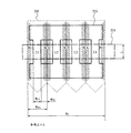
図19は実施例1〜7に基づいて作製される第2形状の半導体領域405を用いてTFTを形成する形態を示すものであり、ゲート電極との位置関係を説明するものである。図19(A)は第2形状の半導体領域405は並列に配置された複数の矩形状の半導体領域と、該矩形状の半導体領域を連接する一対の半導体領域が一体形成された形状であり、ゲート電極417は複数の矩形状の半導体領域と交差するように設けられる。図19(B)はそのA−A'線の沿った縦断面図であり、図19(C)はB−B'線に沿った縦断面図である。
【0081】
図19で示すTFTの特徴は、ゲート電極417が複数の矩形状の半導体領域の上面のみならず側面に回り込むことにより、電界効果が広い面積にわたり、チャネル幅が実質的に増加する。即ち、チャネル幅は図19(C)で示すC1〜C3の半導体領域の幅ではなく、その厚さ方向の成分も考慮する必要がある。
【0082】
図19(B)で示すように、この第2形状の半導体領域405にはチャネル形成領域420、低濃度ドレイン領域418、ソース及びドレイン領域419が形成される。図24はその等価回路を示し、ソース及びドレイン領域の間に複数のチャネルが並列して設けられ一つのトランジスタを形成している。このように、チャネル形成領域を並列に設けることにより、ソース及びドレイン領域の抵抗、及び/又は低濃度ドレイン領域の抵抗により帰還がかかり、各チャネル間に流れる電流を平準化することができる。このような構成のトランジスタにより、複数の素子間での特性の分散を小さくすることができる。
【0083】
[実施例9]
本実施例では、実施例1乃至実施例8により作製される絶縁表面上の第2形状の半導体領域を用いて、CMOS型のTFTを作製する一例について、図20を参照して説明する。
【0084】
図20(A)はガラス基板701、ブロッキング層702が形成された上に活性層とする第2形状の半導体領域703a、703b、ゲート絶縁膜704、ゲート電極705a、705bが形成された状態を示している。ゲート絶縁膜907はプラズマCVD法を用いて、SiH4とN2OにO2を反応ガスとして酸窒化珪素膜で形成し、80nmの厚さとする。第2形状の半導体領域705a、705bは、結晶の配向率が高いため、その上に形成するゲート絶縁膜の膜質のバラツキを少なくすることができ、そのためTFTのしきい値電圧のバラツキを小さくすることができる。また、ゲート電極を形成する材料としてはAl、Ta、Ti、W、Moなどの導電性材料又はこれらの合金を適用し、400nmの厚さに形成する。Alをゲート電極とし、その表面を陽極酸化により酸化膜を形成して安定化しても良い。
【0085】
図20(B)は不純物領域の形成であり、イオンドーピング法によりnチャネル型TFTに対するソース又はドレイン領域706、低濃度ドレイン(LDD)領域707、及びpチャネル型TFTに対するソース又はドレイン領域708を形成する。
【0086】
イオンドーピングにより、不純物元素を注入した領域は結晶性が破壊され、非晶質化する。結晶性の回復と、不純物元素の活性化による低抵抗化を実現するために、レーザー処理を行う。レーザー処理は本発明のレーザー処理装置によって行うことができる。また、水素雰囲気(還元雰囲気)中でレーザー照射を行って水素化を兼ねておこなっても良い。
【0087】
その後、図20(C)に示すように窒化珪素膜又は酸化珪素膜で層間絶縁膜710を形成する。さらに酸化珪素膜や有機樹脂膜、誘電率4以下の低誘電率材料を用いて層間絶縁膜711を形成する。有機樹脂材料としてはアクリル、ポリイミドなどを適用することができる。低誘電率材料としては、SiOF、poly-arylethers、BCB(ベンゾシクロブテン)、フッ化ポリイミド、a−CFなどを適用することができる。次いで、各半導体層の不純物領域に達するコンタクトホールを形成し、Al、Ti、Taなどを用いて配線713、714を形成する。
【0088】
こうしてnチャネル型TFTとpチャネル型TFTを形成することができる。ここではそれぞれのTFTを単体として示しているが、これらのTFTを使ってCMOS回路やNMOS回路、PMOS回路を形成することができる。本発明により形成される活性層はチャネル長方向と平行に結晶成長が成されるので、実質的にキャリアが横切る結晶粒界が無くなり、高い電界効果移動度を得ることができる。こうして作製されるTFTは、アクティブマトリクス型の液晶表示装置や発光素子を用いた表示装置を作製するためのTFTとして、また、ガラス基板上にメモリやマイクロプロセッサを形成するためのTFTとして用いることができる。
【0089】
[実施例10]
図21は発光素子を各画素に設けるアクティブマトリクス駆動方式の表示装置の構成を説明する一例である。実施例9により作製されるTFTにより、画素部1302とその周辺部にある駆動回路部1301を形成することができる。図22はその画素部における構成を示す上面図であり、図21と同じ符号が付与されている。TFTのチャネル形成領域を形成する絶縁表面上に形成された第2形状の半導体領域は、実施例1乃至実施例8を適宜用いて形成される。
【0090】
基板1101はガラス基板又は有機樹脂基板が採用される。有機樹脂材料はガラス材料と比較して軽量であり、発光装置自体の軽量化に有効に作用する。発光装置を作製する上で適用できるものとしては、ポリイミド、ポリエチレンテレフタレート(PET)、ポリエチレンナフタレート(PEN)、ポリエーテルサルフォン(PES)、アラミド等の有機樹脂材料を用いることができる。ガラス基板は無アルカリガラスと呼ばれる、バリウムホウケイ酸ガラスやアルミノホウケイ酸ガラスを用いることが望ましい。ガラス基板の厚さは0.5〜1.1mmのものが採用されるが、軽量化を目的とすると厚さは薄くする必要がある。また、さらに軽量化を図るには比重が2.37g/ccと小さいものを採用することが望ましい。
【0091】
図21では駆動回路部1301にnチャネル型TFT1303とpチャネル型TFT1304が形成され、画素部1302にはnチャネル型TFTで形成される第1TFT1305とpチャネル型TFTで形成される第4TFT1306が形成された構成を示している。そして、第4TFT1306は発光素子1309と接続する構成となっている。
【0092】
これらのTFTは、窒化珪素又は酸窒化珪素から成るブロッキング層1102上に第2形状の半導体領域1103〜1106、ゲート絶縁膜1108、ゲート電極1110〜1113により構成されるものである。ゲート電極の上層には、水素を含有する窒化珪素又は酸窒化珪素からなる第1絶縁層1114が形成され、ブロッキング層1102と合わせて第2形状の半導体領域に水分や金属などの不純物が拡散して汚染されないようにする保護膜として機能している。
【0093】
第1絶縁層1114上には、平坦化膜としてポリイミド、ポリアミド、ポリイミドアミド、アクリル、BCBなど有機樹脂材料から選択される第2絶縁層1115が0.5〜1μmの厚さで形成されている。第2絶縁層1115は、スピン塗布法で当該有機化合物を塗布した後焼成によって形成する。有機絶縁体材料は吸湿性があり、水分を吸蔵する性質を持っている。その水分が再放出されると、この上層部に形成される発光素子の有機化合物に酸素を供給して発光素子を劣化させる原因となる。水分の吸蔵及び再放出を防ぐため、第2絶縁層1115の上に第3絶縁層1116を50〜200nmの厚さで形成する。第3絶縁層1116は下地との密着性及びバリア性の観点から緻密な膜とする必要があり、好ましくはスパッタリング法で形成される窒化珪素、酸窒化珪素、酸窒化アルミニウム、窒化アルミニウム等から選択される無機絶縁材料で形成する。
【0094】
窒素のみをスパッタガスとして用い珪素をターゲットして用いてスパッタリング法により作製された窒化珪素膜においては、膜厚が10〜100nm、好ましくは20〜40nmあれば十分である。このスパッタリング技術は、単にターゲットの母材を希ガスイオンで飛散させるのではなく、ターゲット表面を窒化してそれを基板に付着させるという、所謂反応性スパッタリングに近い反応メカニズムを考えることができる。これにより、窒化珪素をターゲットとした時よりも、より緻密な窒化珪素膜を、しかも室温で形成できるという特徴がある。同様に、スパッタリング法で作製される酸窒化アルミニウム膜では、40nm以上に厚さが必要である。
【0095】
その後、コンタクトホールを形成し、配線1117〜1125を形成する。そして、特に画素領域において、コンタクトホールや配線による表面の凹凸を無くすために、第4絶縁層1128を有機樹脂材料で形成する。有機樹脂材料1128は吸湿性があるので、その上にスパッタリング法により窒化珪素膜で形成される第5絶縁層1129を形成する。第4絶縁層1128は画素部1302のみでなく、駆動回路部1301に渡って延在して形成され、配線1117〜1125を覆って形成することで層間絶縁膜としての機能も兼ね備えている。
【0096】
発光素子1309は、第5絶縁層1129上に形成される。基板1101を通して発光する光を放射する構成の表示装置は、第5絶縁層1129上に陽極層1126としてITO(酸化インジウム・スズ)層を形成する。ITOには平坦化や低抵抗化を目的として酸化亜鉛又はガリウムが添加されていても良い。配線1123は画素部において、陽極層1126とコンタクトホールを介して電気的に接続している。
【0097】
画素毎に形成された陽極層1126の端部とコンタクトホールによる凹凸はここで発光素子が短絡しないように保護絶縁膜1130を設ける。この保護絶縁膜1130は酸化珪素膜や窒化珪素膜、酸窒化珪素膜で形成することができる。保護絶縁膜1130は当該有機絶縁体材料を0.5〜2μmの厚さで全面に形成した後、陽極層126に合わせて開口部を形成する。
【0098】
発光素子1309は陽極層1126と、アルカリ金属又はアルカリ土類金属を含む陰極層1132と、その間に形成される発光体を含む有機化合物層1131をもって形成される。発光体を含む有機化合物層1131は一層又は複数の層が積層されて形成されている。各層はその目的と機能により、正孔注入層、正孔輸送層、発光層、電子輸送層、電子注入層等と区別して呼ばれている。これらは、低分子系有機化合物材料、中分子系有機化合物材料、又は高分子系有機化合物材料のいずれか、或いは、両者を適宣組み合わせて形成することが可能である。また、電子輸送性材料と正孔輸送性材料を適宜混合させた混合層、又はそれぞれの接合界面に混合領域を形成した混合接合を形成しても良い。勿論、陽極と陰極とを反転させた画素構造としても良い。
【0099】
陰極層1132は仕事関数の小さいアルカリ金属又はアルカリ土類金属により形成され、マグネシウム(Mg)、リチウム(Li)若しくはカルシウム(Ca)を含む材料を用いる。好ましくはMgAg(MgとAgをMg:Ag=10:1で混合した材料)でなる電極を用いれば良い。他にもMgAgAl電極、LiAl電極、また、LiFAl電極が挙げられる。又は、アルカリ金属又はアルカリ土類金属のフッ化物とアルミニウムなどの低抵抗金属とを組み合わせて形成しても良い。陰極層1132は共通電極として複数の画素の渡って形成され、画素部1302の外側、或いは画素部1302と駆動回路部1301との間で配線1120に接続され、外部端子に導かれる。
【0100】
さらに気密性を高めるために、その上層には、窒化珪素、ダイヤモンドライクカーボン(DLC)、酸窒化アルミニウム、酸化アルミニウム、窒化アルミニウムなどから選択される材料で第6絶縁層1133を形成しても良い。特に、DLC膜は酸素、CO、CO2、H2O等のガスバリア性が高いことが知られている。第5無機絶縁層は、陰極131を形成した後、大気解放しないで連続的に形成することが望ましい。第5無機絶縁層の下層には窒化珪素のバッファ層を設け密着性を向上させても良い。また、同様に図示されていないが、陽極層1126と発光体を含む有機化合物層1131との界面に0.5〜5nmでトンネル電流が流れる程度の厚さの無機絶縁層を形成しておいても良い。これは陽極表面の凹凸に起因する短絡の防止と、陰極に用いるアルカリ金属等が下層側に拡散するのを抑止する効果がある。
【0101】
図21では第1TFT1305をマルチゲート構造とし、且つ、低濃度ドレイン(LDD)を設けオフ電流を低減させている。第4TFT1306にはゲート電極とオーバーラップするLDDを設けている。多結晶珪素を用いたTFTは、高い動作速度を示すためホットキャリア効果による劣化が起こりやすい。そのため、図21のように、画素内において機能に応じて構造の異なるTFT(オフ電流の十分に低いスイッチング用TFTと、ホットキャリア注入に強い電流制御用TFT)を形成することは、高い信頼性を有し、且つ、良好な画像表示が可能な(動作性能の高い)表示装置を作製する上で非常に有効である。この画素部における上面図は図22で示されている。図22ではほぼ1画素分の構成を示し、第1TFT1305、第2TFT1311、第3TFT1312、第4TFT1306、容量部1312が設けられている。その等価回路図を図24に示す。
【0102】
勿論、ここで示す画素の構成は一例であり、本発明を構成するための必須要件とはならない。
【0103】
駆動回路部1301の回路構成は、ゲート信号側駆動回路とデータ信号側駆動回路とで異なるがここでは省略する。nチャネル型TFT1303及びpチャネル型TFT1304には配線1118、1119が接続され、これらのTFTを用いて、シフトレジスタやラッチ回路、バッファ回路等が形成することが可能である。
【0104】
入力端子部1308はゲート電極と同一層で形成される配線又は第3絶縁層1116上に形成される配線で形成される。図21ではゲート電極と同一層で形成する一例を示し、導電層1109と1127で形成されている。導電層1127は陽極層1126と同時に形成されるものであり、酸化物導電性材料で形成される。実際には表面に露出する部分をこの酸化物導電性材料で覆うことにより、酸化反応による表面抵抗の増大を防いでいる。
【0105】
この開口部及びその周辺には接着性の樹脂1134が充填され、封止板1134が固着される。封止板1135にはステンレス鋼やアルミニウムなどの金属を用いることができる。また、ガラス基板などを適用しても良い。接着性の樹脂1134と封止板1135で囲まれた内側には、酸化バリウムなどの乾燥剤を封入して、水分による劣化を防ぐこともできる。封止板の厚さは30〜120μm程度の有機樹脂材料を使って可撓性を持たせても良い。その表面にはガスバリア層としてDLCや窒化珪素など無機絶縁体から成る被膜を形成しておいても良い。シールパターンに用いられる材料の一例はエポキシ系接着剤であり、その側面部も無機絶縁体から成る被膜で覆うことによりその部分から浸透する水蒸気を防ぐことができる。
【0106】
接着性の樹脂1134としては、紫外線硬化型アクリル樹脂や、カチオン紫外線硬化型エポキシ樹脂を用いることができる。
【0107】
このように、TFTと発光素子を組み合わせて画素部を形成し、表示装置を完成させることができる。このような表示装置はTFTを用いて駆動回路を同一基板上に形成することもできる。図21で示すように、TFTの主要構成要素である半導体膜、ゲート絶縁膜及びゲート電極を、その下層側及び上層側を窒化珪素又は酸窒化珪素から成るブロッキング層と保護膜により囲むことにより、アルカリ金属や有機物の汚染を防ぐ構造を有している。一方発光素子はアルカリ金属を一部に含み、窒化珪素又は酸窒化珪素又はDLC膜から成る保護膜と、窒化珪素又は炭素を主成分とする絶縁膜から成るガスバリア層とで囲まれ、外部から酸素や水分が浸入することを防ぐ構造を有している。
【0108】
[実施例11]
本発明を用いて作製されるTFTを搭載した半導体装置は、様々な適用が可能である。その一例は、携帯情報端末(電子手帳、モバイルコンピュータ、携帯電話等)、ビデオカメラ、デジタルカメラ、パーソナルコンピュータ、テレビ受像器、携帯電話、投影型表示装置等が挙げられる。それらの一例を図25、図26に示す。
【0109】
図25(A)は本発明を適用してテレビ受像器を完成させる一例であり、筐体3001、支持台3002、表示部3003等により構成されている。本発明により作製されるTFTは表示部3003に適用され、本発明によりテレビ受像器を完成させることができる。
【0110】
図25(B)は本発明を適用してビデオカメラを完成させた一例であり、本体3011、表示部3012、音声入力部3013、操作スイッチ3014、バッテリー3015、受像部3016等により構成されている。本発明により作製されるTFTは表示部3012に適用され、本発明によりビデオカメラを完成させることができる。
【0111】
図25(C)は本発明を適用してノート型のパーソナルコンピュータを完成させた一例であり、本体3021、筐体3022、表示部3023、キーボード3024等により構成されている。本発明により作製されるTFTは表示部3023に適用され、本発明によりパーソナルコンピュータを完成させることができる。
【0112】
図25(D)は本発明を適用してPDA(Personal Digital Assistant)を完成させた一例であり、本体3031、スタイラス3032、表示部3033、操作ボタン3034、外部インターフェース3035等により構成されている。本発明により作製されるTFTは表示部3033に適用され、本発明によりPDAを完成させることができる。
【0113】
図25(E)は本発明を適用して音響再生装置を完成させた一例であり、具体的には車載用のオーディオ装置であり、本体3041、表示部3042、操作スイッチ3043、3044等により構成されている。本発明により作製されるTFTは表示部3042に適用され、本発明によりオーディオ装置を完成させることができる。
【0114】
図25(F)は本発明を適用してデジタルカメラを完成させた一例であり、本体3051、表示部(A)3052、接眼部3053、操作スイッチ3054、表示部(B)3055、バッテリー3056等により構成されている。本発明により作製されるTFTは表示部(A)3052および表示部(B)3055に適用され、本発明によりデジタルカメラを完成させることができる。
【0115】
図25(G)は本発明を適用して携帯電話を完成させた一例であり、本体3061、音声出力部3062、音声入力部3063、表示部3064、操作スイッチ3065、アンテナ3066等により構成されている。本発明により作製されるTFTは表示部3064に適用され、本発明により携帯電話を完成させることができる。
【0116】
図26(A)はフロント型プロジェクターであり、投射装置2601、スクリーン2602等を含む。図26(B)はリア型プロジェクターであり、本体2701、投射装置2702、ミラー2703、スクリーン2704等を含む。
【0117】
尚、図26(C)は、図26(A)及び図26(B)中における投射装置2601、2702の構造の一例を示した図である。投射装置2601、2702は、光源光学系2801、ミラー2802、2804〜2806、ダイクロイックミラー2803、プリズム2807、液晶表示装置2808、位相差板2809、投射光学系2810で構成される。投射光学系2810は、投射レンズを含む光学系で構成される。本実施例は三板式の例を示したが、特に限定されず、例えば単板式であってもよい。また、図26(C)中において矢印で示した光路に実施者が適宜、光学レンズや、偏光機能を有するフィルムや、位相差を調節するためのフィルム、IRフィルム等の光学系を設けてもよい。
【0118】
また、図26(D)は、図26(C)中における光源光学系2801の構造の一例を示した図である。本実施例では、光源光学系2801は、リフレクター2811、光源2812、レンズアレイ2813、2814、偏光変換素子2815、集光レンズ2816で構成される。なお、図26(D)に示した光源光学系は一例であって特に限定されない。例えば、光源光学系に実施者が適宜、光学レンズや、偏光機能を有するフィルムや、位相差を調節するフィルム、IRフィルム等の光学系を設けてもよい。
【0119】
尚、ここで示す装置はごく一例であり、これらの用途に限定するものではないことを付記する。
【0120】
【発明の効果】
以上、説明したように本発明によれば、一辺に、先の尖った凸端部を有する半導体領域を複数個並列に配置された第1形状の半導体領域を用いて連続発振レーザー光を照射して結晶化させることにより、結晶成長はシード領域に最初に形成される結晶を核としてその結晶が成長し、結晶の核生成は制限を受け、核生成密度を低減させると共に結晶の配向を制限する効力を持たせることにより、特定の方位を持った結晶を成長させることができる。そして、複数の凸端部から延在する結晶で形成されるように配設して、凹部から延びる結晶粒界や歪みが蓄積された結晶を除去することにより、良質の結晶のみでTFTを形成することができる。
【0121】
このような構成とし、複数の矩形状の半導体領域を複数個並列に配設し、一対のソース及びドレイン領域間に設け、一つのトランジスタを形成することで、素子間の特性の分散を小さくすることができる。また、良質な結晶のみを使うことで、電界効果移動度を向上させることができる。
【図面の簡単な説明】
【図1】 本発明の半導体装置の作製方法の概念を説明する図。
【図2】 本発明に係る結晶化工程の詳細を説明する図。
【図3】 本発明に係る結晶化工程の詳細を説明する図。
【図4】 本発明に係る結晶化工程の詳細を説明する図。
【図5】 本発明に係る結晶化工程の詳細を説明する図。
【図6】 本発明に係る結晶化工程の詳細を説明する図。
【図7】 本発明に適用するレーザー照射装置の一態様を示す配置図。
【図8】 本発明に係る結晶化法を説明する上面及び断面図。
【図9】 本発明に係る結晶化法を説明する上面及び断面図。
【図10】 本発明に係る結晶化法を説明する上面及び断面図。
【図11】 本発明に係る結晶化法を説明する上面及び断面図。
【図12】 本発明に係る結晶化法を説明する断面図。
【図13】 本発明に係る結晶化法を説明する上面及び断面図。
【図14】 本発明に係る結晶化法を説明する断面図。
【図15】 本発明に係る結晶化法を説明する断面図。
【図16】 本発明に係る結晶化法を説明する上面及び断面図。
【図17】 本発明に係る結晶化法を説明する断面図。
【図18】 本発明に係る結晶化法を説明する上面及び断面図。
【図19】 本発明に係る結晶化法で形成された結晶性半導体膜を用いたTFTの構造を説明する上面及び断面図。
【図20】 本発明に係る結晶化法で形成された結晶性半導体膜を用いたTFTの作製工程を説明する断面図。
【図21】 本発明により作製されるTFTを用いた表示装置の画素構造を示す面図。
【図22】 本発明により作製されるTFTを用いた表示装置の画素構造を示す上面図。
【図23】 本発明に係る結晶化法を説明するものであり、第1形状の半導体領域と結晶成長の関連を説明する図である。
【図24】 本発明により作製されるTFTの等価回路図。
【図25】 半導体装置の一例を示す図。
【図26】 プロジェクターの一例を示す図。[0001]
BACKGROUND OF THE INVENTION
The present invention relates to a semiconductor device using a crystalline semiconductor film that is crystallized by irradiating an amorphous semiconductor film with laser light, and a manufacturing method thereof.
[0002]
[Prior art]
A technique for crystallizing an amorphous semiconductor film formed on a substrate such as glass by laser treatment is known. Laser treatment refers to a technique for recrystallizing a damaged layer or an amorphous layer formed on a semiconductor substrate or semiconductor film, a technique for crystallizing an amorphous semiconductor film formed on an insulating surface, or a crystal structure. This refers to a technique for improving the crystallinity of a semiconductor film (crystalline semiconductor film). As a laser oscillation device used for laser processing, a gas laser typified by an excimer laser or a solid-state laser typified by a YAG laser is usually used.
[0003]
The feature of using laser light is that it can selectively heat only the region that is irradiated with laser light and absorbs the energy of the laser light, compared to heat treatment using radiation heating or conduction heating. is there. For example, laser processing using an excimer laser oscillating device selectively and locally heats a semiconductor film to realize crystallization and activation processing of the semiconductor film with almost no thermal damage to the glass substrate. Yes.
[0004]
Examples of laser treatment include a method of uniformly irradiating laser light on the entire surface of an object to be irradiated as disclosed in JP-A-2-181419, and a spot-like beam disclosed in JP-A-62-104117. Or a method of processing and irradiating a linear beam with an optical system as in a laser processing apparatus disclosed in Japanese Patent Application Laid-Open No. 8-195357 is known.
[0005]
In the above Japanese Patent Application Laid-Open No. 62-104117, a technique for polycrystallizing an amorphous semiconductor film without bringing it into a completely melted state by high speed scanning with a laser beam scanning speed of beam spot diameter × 5000 / second or more. Is disclosed. U.S. Pat. No. 4,330,363 discloses a technique for substantially forming a single crystal region by irradiating a semiconductor region formed in an island shape with an extended laser beam.
[0006]
Nd: YVO Four A crystallization technique using a solid-state laser oscillation device such as a laser is disclosed in Japanese Patent Application Laid-Open No. 2001-144027. In this publication, it is disclosed that a crystalline semiconductor film having a larger crystal grain size than before can be obtained by using the second harmonic of the laser light emitted from the solid-state laser oscillation device.
[0007]
In particular, the application to thin film transistors (hereinafter referred to as TFTs) in crystallization technology using a continuous-wave solid-state laser oscillator is described in "" Ultra-high Performance Poly-Si TFTs on a Glass by a Stable Scanning CW Laser Lateral Crystallization ", A. Hara, F. Takeuchi, M. Takei, K. Yoshino, K. Suga and N. Sasaki, AMLCD '01 Tech. Dig., 2001, pp. 227-230. This is a diode-pumped solid state continuous wave laser (YVO). Four An example of manufacturing a TFT using a polycrystalline silicon film crystallized using the second harmonic of (1) is disclosed.
[0008]
[Problems to be solved by the invention]
When the amorphous semiconductor film formed on the insulating surface is crystallized by irradiating the continuous wave laser beam, a crystal having a relatively large grain size can be formed even on the glass substrate. However, the entire surface of the substrate could not be oriented in a single crystal orientation. For specific crystal grains, the same orientation could be confirmed, but not all crystal grains in the crystallization region could be aligned.
[0009]
Regardless of pulse oscillation or continuous oscillation, most of the crystallization of the amorphous semiconductor film by the pulse laser beam grows through a melting-solidification process. In detail, it is considered that it is divided into stages of generation of crystal nuclei and crystal growth from the nuclei. However, most of the conventional methods cannot control the generation position and generation density of crystal nuclei, and perform crystallization using naturally occurring crystal nuclei. Therefore, there has been a problem that crystals cannot be grown with a specific orientation. Therefore, the crystal grains are formed at an arbitrary position within the surface of the glass substrate, and only a small size of about 0.2 to 0.5 μm is obtained.
[0010]
Usually, a large number of defects are generated at the crystal grain boundary, which is considered to be a factor that limits the field effect mobility of the TFT. Further, depending on crystal nuclei generated arbitrarily, the crystal orientation becomes random, and a crystalline semiconductor with uniform orientation cannot be obtained.
[0011]
In laser processing using a pulsed laser oscillator, crystal growth due to crystal nuclei becomes dominant, and it is impossible to realize a large crystal grain size. Specifically, it is not possible to form a crystal that can be regarded substantially as a single crystal when viewed at the element level, in which no crystal grain boundary exists in the channel formation region of the TFT. The generated defects or dislocations are not limited to the crystal grain boundaries, but are generated when the film volume shrinks due to densification accompanying crystallization.
[0012]
On the other hand, the method of crystallization while melting and solidifying by scanning continuous wave laser light is considered to be a method close to the zone melting method, and it is considered that a large particle size can be obtained by continuous crystal growth. It has been. However, there is a problem that the quality of the obtained crystal depends on the crystallinity of the region to be crystallized first. Specifically, crystal growth is performed in the hope of accidental crystal nuclei.
[0013]
As described above, in the conventional crystallization method using laser light, the dispersion (or variation) of TFT characteristics is a major factor, which suppresses the performance of various semiconductor devices having TFTs as components of electronic circuits. It has become.
[0014]
The present invention has been made in view of such problems, and improves the crystallinity of a crystalline semiconductor film formed by crystallizing an amorphous semiconductor film, thereby realizing a TFT capable of operating at higher speed. For the purpose.
[0015]
[Means for Solving the Problems]
In order to solve the above problems, the present invention forms a first shape semiconductor region in an island shape on an insulating surface, crystallizes the region with continuous wave laser light, and forms an inner portion of the first shape semiconductor region. Is used to form a second-shaped semiconductor region as an active layer such as a TFT. In order to reduce the dispersion of characteristics of a device manufactured using a crystalline semiconductor film, it is necessary to homogenize the crystallinity of an active region that determines the characteristics of the device. For this purpose, the present invention devised the shape of the region that is the starting point for crystallization in the semiconductor region of the first shape.
[0016]
Specifically, a first-shaped semiconductor region having a plurality of pointed convex ends is formed on one side, and a continuous wave laser beam is irradiated from that region, thereby scanning the laser beam. direction The first shape semiconductor region is crystallized or improved in crystallinity. As the laser light, it is preferable to use one or a plurality of continuous wave laser beams that are condensed linearly on the irradiation surface. Thereafter, the first shape semiconductor region is etched to form a second shape semiconductor region in which a channel formation region and source and drain regions are formed. In the second shape semiconductor region, a strip-shaped semiconductor region is arranged so that a channel formation region is formed in each of the crystal regions extending from the plurality of convex ends, and the semiconductor region adjacent to the channel formation region is removed. As shown, the etching process is performed using a photolithography technique.
[0017]
Alternatively, from a semiconductor film formed on an insulating surface, a first-shaped semiconductor region in which a plurality of semiconductor regions each having a pointed convex end are arranged in parallel on one side is formed, and continuous oscillation is started from that region. It can also be said that by irradiating the laser beam, the semiconductor region of the first shape is crystallized or improved in crystallinity along the scanning walk of the laser beam.
[0018]
It is desirable that the continuous wave laser beam condensed in a linear shape has an energy density distribution that is uniform in the longitudinal direction. An arbitrary distribution may be provided in the short direction, and for example, a Gaussian distribution or the like may be provided. The laser treatment is performed by scanning in a direction intersecting with the longitudinal direction of the continuous wave laser beam condensed linearly. At this time, scanning is performed by having a uniform intensity distribution in the longitudinal direction. Crystal growth that extends parallel to the direction is possible. That is, if there is a non-uniform energy density distribution in the longitudinal direction, a temperature gradient occurs, and a disordered crystal is formed in which the crystal extends depending on the temperature gradient.
[0019]
Such a continuous wave laser light source is a rectangular beam solid state laser oscillation device, and a slab laser oscillation device can be typically used.
[0020]
In the second shape semiconductor region Oh The interval between adjacent strip-shaped semiconductor regions is preferably at least twice the length of the semiconductor region in the channel width direction, and is preferably 0.5 to 1.0 μm in view of crystal growth. In this strip-shaped semiconductor region, a channel formation region is provided by forming a low-concentration drain region or an electrode to which a common potential is applied via an insulating film.
[0021]
As described above, the TFT having the second shape semiconductor region formed after the first shape semiconductor region is crystallized or improved in crystallinity includes a plurality of rectangular semiconductor regions arranged in parallel and the rectangular shape. A plurality of rectangular semiconductor regions each having a channel formation region formed by electrodes intersecting with each other through an insulating film; The crystal extends along the channel length direction.
[0022]
Alternatively, a plurality of rectangular semiconductor regions arranged in parallel are connected in series and a crystalline semiconductor film in which a pair of semiconductor regions connected to both ends thereof are integrally formed, and the plurality of rectangular semiconductor regions are A channel formation region is formed by electrodes intersecting with each other through an insulating film, and crystals extend along the channel length direction.
[0023]
A crystal of a rectangular semiconductor region provided with a channel formation region is characterized by extending in a direction parallel to the channel length direction or having a uniform crystal orientation. In addition, each of the plurality of rectangular semiconductor regions is disposed with an interval of at least twice the length in the channel width direction.
[0024]
That is, in the second-shaped semiconductor region, the region for forming the channel formation region of the TFT is disposed so as to be formed of a high-quality crystal extending from a plurality of pointed convex end portions in the one end region. To do. Alternatively, the region is etched and removed so that a crystal grain boundary extending from the recess or a crystal in which strain is accumulated is not applied to the channel formation region.
[0025]
With such a structure, a plurality of rectangular semiconductor regions are arranged in parallel, provided between a pair of source and drain regions, and a single transistor is formed to reduce dispersion of characteristics between elements. be able to. In addition, field effect mobility can be improved by using only high-quality crystals.
[0026]
Note that the amorphous semiconductor film referred to in the present invention is not limited to a film having a completely amorphous structure, but includes a state in which fine crystal particles are included, or a so-called microcrystalline semiconductor film, local In particular, a semiconductor film including a crystal structure is included. Typically, an amorphous silicon film is applied, and in addition, an amorphous silicon germanium film, an amorphous silicon carbide film, or the like can also be applied.
[0027]
DETAILED DESCRIPTION OF THE INVENTION
Embodiments of the present invention will be described below with reference to the drawings. The perspective view shown in FIG. 1A shows a state where a
[0028]
A mask pattern is formed over the
[0029]
The shape of the first-shaped
[0030]
The continuous
[0031]
As the slab material, crystals such as Nd: YAG, Nd: GGG (gadolinium / gallium / garnet), Nd: GsGG (gadolinium / scandium / gallium / garnet) are used. A slab laser travels in a zigzag optical path through this plate-like laser medium while repeating total reflection.
[0032]
The wavelength of the continuous wave laser beam is preferably 400 to 700 nm in consideration of the light absorption coefficient of the amorphous semiconductor film. Light in such a wavelength band is obtained by taking out the second harmonic and the third harmonic of the fundamental wave using a wavelength conversion element. As wavelength conversion element, ADP (ammonium dihydrogen phosphate), Ba 2 NaNb Five O 15 (Sodium barium niobate), CdSe (selenium cadmium), KDP (potassium dihydrogen phosphate), LiNbO Three (Lithium niobate), Se, Te, LBO, BBO, KB5 and the like are applied. It is particularly desirable to use LBO. A typical example is Nd: YVO Four The second harmonic (532 nm) of the laser oscillation device (fundamental wave 1064 nm) is used. The laser oscillation mode is TEM 00 Apply single mode.
[0033]
In the case of silicon selected as the most suitable material, the absorption coefficient is 10 Three -10 Four cm -1 The region which is is almost in the visible light region. When crystallizing a substrate having a high visible light transmittance, such as glass, and the first-shaped
[0034]
The laser beam irradiation method may be from the side where the first-shaped
[0035]
The characteristic shape of the first
[0036]
On the other hand, the crystals extending from the concave portions formed between the convex portions interfere with each other because the crystals growing from both ends interfere with each other, thereby inhibiting the growth of high-quality crystals. In other words, growth based on a plurality of crystal nuclei occurs simultaneously and interfere with each other, thereby growing a crystal in which crystal grain boundaries and strain are accumulated.
[0037]
Thereafter, as shown in FIG. 1C, a second shape semiconductor region 108 is formed by etching. In the second shape semiconductor region 108, a region for forming a channel formation region of the TFT is formed by a plurality of pointed convex ends in the
[0038]
Therefore, the second-shaped semiconductor region 108 can be regarded as a shape in which a plurality of rectangular semiconductor regions arranged in parallel and a pair of semiconductor regions connecting the rectangular semiconductor regions are integrally formed. In each of the plurality of rectangular semiconductor regions, a channel forming region can be formed there by providing electrodes that intersect with each other through an insulating film. Alternatively, this shape can be regarded as a shape in which a plurality of rectangular semiconductor regions arranged in parallel are connected in series and a pair of semiconductor regions connected to both ends thereof are integrally formed. In addition, each of the plurality of rectangular semiconductor regions is disposed with an interval of at least twice as long as the length in the channel width direction. The plurality of rectangular semiconductor regions have a feature that they extend in a direction parallel to the channel length direction or have a uniform crystal orientation in the channel formation region.
[0039]
FIG. 2 shows a top view of the first-shaped semiconductor region. Crystallization is performed by scanning the continuous
[0040]
Crystal growth proceeds from both the convex end portion (seed region) 202 and the concave portion therebetween, but the nucleation density of the crystal is limited by the sharp shape from the convex end portion (seed region) 202, and the nucleation density It is possible to grow a crystal having a specific orientation by reducing the crystallinity and limiting the orientation of the crystal. On the other hand, a crystal extending from a concave portion formed between convex portions simultaneously grows based on a plurality of crystal nuclei, and interferes with each other to grow a crystal with accumulated grain boundaries and strain. Become.
[0041]
Further, the continuous wave laser beam to be irradiated is not limited to a single linear laser beam, and even if a plurality of continuous
[0042]
FIG. 4 is a top view illustrating the first-shaped
[0043]
The first-shaped
[0044]
As shown in FIG. 5, the second
As shown by a dotted line in the figure, the
[0045]
FIG. 6 is an example of another configuration, in which a second
[0046]
FIG. 23 shows another example of the shape of the preferred first shape semiconductor region. The basic form shown in FIG. 23A is the first shape. In other words, the shape where the two opposite sides of the pentagon are serrated The
[0047]
Crystallization by the continuous
[0048]
FIG. 23B illustrates a structure in which the first
[0049]
An example of the configuration of a laser processing apparatus that can be applied to the present invention is shown in FIG. FIG. 7 shows a
[0050]
Laser light condensed linearly in the cross-sectional shape of the irradiation surface by the
[0051]
As described above, a rectangular beam solid-state laser oscillation device is applied as the laser oscillation device, and a slab laser oscillation device is particularly preferably applied. Or YAG, YVO Four , YLF, YAlO Three A slab structure amplifier may be combined with a solid-state laser oscillation device using a crystal doped with Nd, Tm, or Ho. As the slab material, crystals such as Nd: YAG, Nd: GGG (gadolinium / gallium / garnet), Nd: GsGG (gadolinium / scandium / gallium / garnet) are used. In addition, a gas laser oscillation device and a solid laser oscillation device capable of continuous oscillation can also be applied. As continuous wave solid state laser oscillator, YAG, YVO Four , YLF, YAlO Three A laser oscillation device using a crystal doped with Cr, Nd, Er, Ho, Ce, Co, Ti, or Tm is applied. The fundamental wave of the oscillation wavelength varies depending on the material to be doped, but oscillates at a wavelength of 1 μm to 2 μm. In order to obtain a higher output, a diode-pumped solid state laser oscillation device may be applied and cascaded.
[0052]
In addition, the
[0053]
The laser light irradiated onto the
[0054]
【Example】
Hereinafter, specific examples of a method for manufacturing a semiconductor device according to the present invention will be described in detail with reference to the drawings.
[0055]
[Example 1]
In this embodiment, an amorphous silicon film formed on an insulating surface is etched into a predetermined pattern by photolithography to form a first shape semiconductor region, which is crystallized by a continuous wave laser beam. is there.
[0056]
In FIG. 8, a
[0057]
A region (seed region) 404 provided with a plurality of pointed convex ends is formed at one end of the first-shaped
[0058]
FIG. 9 is a diagram showing a stage of crystallization by continuous wave laser light. Although the irradiation area of the
[0059]
In this way, crystallization proceeds from the region irradiated with the
[0060]
Then, as shown in FIG. 9, the crystallized first
[0061]
In such a crystallization method, crystal growth in which crystal grains extend in a single direction is enabled by irradiating continuous wave laser light. Of course, it is necessary to appropriately set detailed parameters such as the scanning speed and energy density of the laser beam, but this can be realized by setting the scanning speed to 5 to 100 cm / sec. The crystal growth rate after melting and solidification using a pulsed laser is said to be 1 m / sec, but the continuous crystal at the solid-liquid interface is scanned by scanning the laser beam at a slower rate and cooling it slowly. Growth is possible, and a large crystal grain size can be realized.
[0062]
[Example 2]
The laser beam scanning in the first embodiment may be reciprocal scanning instead of scanning in only one direction. FIG. 11 shows such an embodiment. In that case, the seed regions 404 a and 404 b may be provided at both ends of the first-shaped
[0063]
[Example 3]
In this embodiment, an amorphous silicon film formed on an insulating surface is crystallized in advance, and the crystal grain size is increased by a continuous wave laser beam.
[0064]
As shown in FIG. 12A, a
[0065]
Thereafter, as shown in FIG. 12B, the amorphous silicon film is crystallized by heat treatment at 580 ° C. for 4 hours. Crystallization grows in the direction parallel to the substrate surface from the
[0066]
After the heat treatment is completed, the
[0067]
Thereafter, as shown in FIG. 13, the
[0068]
The crystalline silicon film is melted and recrystallized by such laser light irradiation. Along with this recrystallization, crystal growth is performed in which crystal grains extend in the scanning direction of the laser beam. In this case, since a crystalline silicon film having a uniform crystal plane is formed in advance, it is possible to prevent the precipitation of crystals on different planes and the occurrence of dislocations. Thereafter, the TFT can be formed by the same process as in the first embodiment.
[0069]
[Example 4]
As shown in FIG. 14A, after forming a
[0070]
Thereafter, the
[0071]
[Example 5]
FIG. (A), FIG. 16 (B) As shown in FIG. 5, after the
[0072]
After that, the
[0073]
[Example 6]
Figure 17 (A) As shown in FIG. 5, after the
[0074]
Thereafter, heat treatment is performed at 450 to 600 ° C. for 1 to 30 minutes using a furnace annealing furnace. Alternatively, heat treatment is performed at 500 to 750 ° C. for 10 to 120 seconds using a rapid thermal annealing (RTA) furnace, and crystal nuclei are formed in the first
[0075]
Then, crystallization is performed by irradiating continuous wave laser light as shown in FIG. Crystallization is characterized in that the orientation is enhanced by the action of crystal nuclei formed in advance, and the applicable range is widened under the irradiation conditions of the continuous wave laser light to be irradiated. This is due to the action of the catalytic element, and is due to a decrease in the nucleation temperature or the crystallization start temperature. Thus, the first
[0076]
[Example 7]
In Example 3 or Example 4, after the
[0077]
As shown in FIG. 15, a
[0078]
Thereafter, Ni added as a catalytic element is obtained by heat treatment at 600 ° C. for 12 hours in a furnace annealing furnace, or heat treatment at 650-750 ° C. for 30-60 minutes by lamp annealing or gas heat annealing. Can be segregated. By this treatment, the concentration of the catalytic element of the
[0079]
After the gettering process is completed, the process may be performed in the same manner as in the third or fourth embodiment. Such gettering may be performed after the first shape semiconductor region is formed, or is effective after the second shape semiconductor region is formed. Further, it may be performed after the crystallization treatment by irradiation with continuous wave laser light. In any case, by performing the gettering in a state where the crystallinity is enhanced, it becomes easier to segregate a catalyst element such as Ni to the gettering site.
[0080]
[Example 8]
FIG. 19 shows a mode in which a TFT is formed using the second-shaped
[0081]
A feature of the TFT shown in FIG. 19 is that the channel width is substantially increased over an area where the field effect is wide because the
[0082]
As shown in FIG. 19B, a
[0083]
[Example 9]
In this embodiment, an example of manufacturing a CMOS TFT using the second shape semiconductor region on the insulating surface manufactured in
[0084]
FIG. 20A shows a state in which second-shaped
[0085]
FIG. 20B shows formation of an impurity region, and a source or drain
[0086]
By ion doping, the region into which the impurity element is implanted is broken in crystallinity and becomes amorphous. Laser treatment is performed in order to recover the crystallinity and reduce the resistance by activating the impurity element. Laser treatment can be performed by the laser processing apparatus of the present invention. Alternatively, laser irradiation may be performed in a hydrogen atmosphere (reducing atmosphere) to perform hydrogenation.
[0087]
After that, as shown in FIG. 20C, an
[0088]
Thus, an n-channel TFT and a p-channel TFT can be formed. Although each TFT is shown here as a single unit, a CMOS circuit, NMOS circuit, or PMOS circuit can be formed using these TFTs. Since the active layer formed according to the present invention undergoes crystal growth parallel to the channel length direction, there is substantially no crystal grain boundary crossed by carriers, and high field effect mobility can be obtained. The TFT thus manufactured can be used as a TFT for manufacturing an active matrix type liquid crystal display device or a display device using a light emitting element, and as a TFT for forming a memory or a microprocessor on a glass substrate. it can.
[0089]
[Example 10]
FIG. 21 illustrates an example of a structure of an active matrix driving display device in which a light-emitting element is provided in each pixel. With the TFT manufactured according to Embodiment 9, the pixel portion 1302 and the driver circuit portion 1301 in the periphery thereof can be formed. FIG. 22 is a top view showing a configuration of the pixel portion, and the same reference numerals as those in FIG. 21 are given. The second-shaped semiconductor region formed on the insulating surface that forms the channel formation region of the TFT is formed using Examples 1 to 8 as appropriate.
[0090]
As the
[0091]
In FIG. 21, an n-
[0092]
These TFTs are constituted by second
[0093]
On the 1st insulating
[0094]
In a silicon nitride film formed by sputtering using only nitrogen as a sputtering gas and targeting silicon, a film thickness of 10 to 100 nm, preferably 20 to 40 nm is sufficient. This sputtering technique can consider a reaction mechanism close to so-called reactive sputtering, in which the target base material is not simply scattered by rare gas ions, but the target surface is nitrided and attached to the substrate. Thus, a denser silicon nitride film can be formed at room temperature than when silicon nitride is used as a target. Similarly, an aluminum oxynitride film manufactured by a sputtering method needs to have a thickness of 40 nm or more.
[0095]
Thereafter, contact holes are formed, and wirings 1117 to 1125 are formed. In particular, in the pixel region, the fourth insulating
[0096]
The
[0097]
A protective
[0098]
The light-emitting
[0099]
The
[0100]
In order to further improve the airtightness, a sixth insulating
[0101]
Figure 21
[0102]
Of course, the structure of the pixel shown here is merely an example, and is not an essential requirement for configuring the present invention.
[0103]
The circuit configuration of the drive circuit unit 1301 differs between the gate signal side drive circuit and the data signal side drive circuit, but is omitted here.
[0104]
The input terminal portion 1308 is formed by a wiring formed in the same layer as the gate electrode or a wiring formed on the third insulating
[0105]
[0106]
As the
[0107]
In this manner, a pixel portion can be formed by combining a TFT and a light emitting element, whereby a display device can be completed. In such a display device, a driver circuit can be formed over the same substrate using TFTs. As shown in FIG. 21, by enclosing the semiconductor film, the gate insulating film, and the gate electrode, which are the main components of the TFT, on the lower layer side and the upper layer side with a blocking layer and a protective film made of silicon nitride or silicon oxynitride, It has a structure that prevents contamination with alkali metals and organic substances. On the other hand, the light-emitting element includes an alkali metal in part, and is surrounded by a protective film made of silicon nitride, silicon oxynitride, or a DLC film, and a gas barrier layer made of an insulating film containing silicon nitride or carbon as a main component. And has a structure that prevents moisture from entering.
[0108]
[Example 11]
A semiconductor device mounted with a TFT manufactured using the present invention can be applied in various ways. Examples thereof include portable information terminals (electronic notebooks, mobile computers, mobile phones, etc.), video cameras, digital cameras, personal computers, television receivers, mobile phones, projection display devices, and the like. Examples of these are shown in FIGS.
[0109]
FIG. 25A illustrates an example in which the present invention is applied to complete a television receiver, which includes a housing 3001, a
[0110]
FIG. 25B shows an example in which the present invention is applied to complete a video camera, which includes a
[0111]
FIG. 25C shows an example in which a laptop personal computer is completed by applying the present invention, which includes a main body 3021, a
[0112]
FIG. 25D is an example in which a PDA (Personal Digital Assistant) is completed by applying the present invention, and includes a
[0113]
FIG. 25E is an example in which a sound reproducing device is completed by applying the present invention, specifically, an in-vehicle audio device, which includes a
[0114]
FIG. 25F is an example in which the present invention is applied to complete a digital camera. A main body 3051, a display portion (A) 3052, an eyepiece portion 3053, an
[0115]
FIG. 25G illustrates an example in which a cellular phone is completed by applying the present invention, which includes a
[0116]
FIG. 26A shows a front projector, which includes a
[0117]
FIG. 26C is a diagram illustrating an example of the structure of the
[0118]
FIG. 26D is a diagram illustrating an example of the structure of the light source
[0119]
It should be noted that the apparatus shown here is only an example and is not limited to these applications.
[0120]
【The invention's effect】
As described above, according to the present invention, continuous wave laser light is irradiated using a first-shaped semiconductor region in which a plurality of semiconductor regions each having a pointed convex end are arranged in parallel on one side. The crystal grows with the crystal first formed in the seed region as the nucleus, and the crystal grows, and the nucleation of the crystal is limited, reducing the nucleation density and limiting the crystal orientation. By having the effect, a crystal having a specific orientation can be grown. Then, the TFT is formed only by a high quality crystal by disposing the crystal grain boundary extending from the concave portion and the crystal in which the distortion is accumulated by disposing the crystal extending from the plurality of convex end portions. can do.
[0121]
With such a structure, a plurality of rectangular semiconductor regions are arranged in parallel, provided between a pair of source and drain regions, and a single transistor is formed to reduce dispersion of characteristics between elements. be able to. In addition, field effect mobility can be improved by using only high-quality crystals.
[Brief description of the drawings]
FIGS. 1A to 1C illustrate a concept of a method for manufacturing a semiconductor device of the present invention. FIGS.
FIG. 2 is a diagram for explaining details of a crystallization step according to the present invention.
FIG. 3 is a diagram for explaining details of a crystallization process according to the present invention.
FIG. 4 is a diagram for explaining details of a crystallization process according to the present invention.
FIG. 5 is a diagram for explaining details of a crystallization process according to the present invention.
FIG. 6 is a diagram for explaining details of a crystallization process according to the present invention.
FIG. 7 is a layout view illustrating one embodiment of a laser irradiation apparatus applied to the present invention.
FIGS. 8A and 8B are a top view and a cross-sectional view illustrating a crystallization method according to the present invention. FIGS.
9A and 9B are a top view and a cross-sectional view illustrating a crystallization method according to the present invention.
10A and 10B are a top view and a cross-sectional view illustrating a crystallization method according to the present invention.
11A and 11B are a top view and a cross-sectional view illustrating a crystallization method according to the present invention.
FIG. 12 is a cross-sectional view illustrating a crystallization method according to the present invention.
13A and 13B are a top view and a cross-sectional view illustrating a crystallization method according to the present invention.
FIG. 14 is a cross-sectional view illustrating a crystallization method according to the present invention.
FIG. 15 is a cross-sectional view illustrating a crystallization method according to the present invention.
16A and 16B are a top view and a cross-sectional view illustrating a crystallization method according to the present invention.
FIG. 17 is a cross-sectional view illustrating a crystallization method according to the present invention.
18A and 18B are a top view and a cross-sectional view illustrating a crystallization method according to the present invention.
FIGS. 19A and 19B are a top view and a cross-sectional view illustrating a structure of a TFT using a crystalline semiconductor film formed by a crystallization method according to the present invention. FIGS.
20 is a cross-sectional view illustrating a manufacturing process of a TFT using a crystalline semiconductor film formed by a crystallization method according to the present invention. FIG.
FIG. 21 is a plan view showing a pixel structure of a display device using a TFT manufactured according to the present invention.
FIG. 22 is a top view illustrating a pixel structure of a display device using a TFT manufactured according to the present invention.
FIG. 23 is a diagram for explaining the crystallization method according to the present invention and explaining the relationship between the first shape semiconductor region and the crystal growth.
FIG. 24 is an equivalent circuit diagram of a TFT manufactured according to the present invention.
FIG 25 illustrates an example of a semiconductor device.
FIG. 26 is a diagram showing an example of a projector.
Claims (10)
前記半導体膜をエッチングすることによって、一方に先の尖った複数の凸端部と、前記複数の凸端部の間に形成された凹部と、前記凸端部および凹部に対向する他方で一体となっている他方の端部とを有する第1形状の半導体領域を形成し、
連続発振レーザー光を前記複数の凸端部から前記他方の端部に向かって走査しながら前記第1形状の半導体領域に照射することによって、前記第1形状の半導体領域を結晶化又は結晶性を向上させ、
前記結晶化又は結晶性を向上させた第1形状の半導体領域が有する前記凹部から他方の端部に向かって延びる結晶領域の一部をエッチング除去することによって、前記第1形状が有する複数の凸端部から他方の端部に向かって延びる結晶領域で形成された複数の矩形状の半導体領域と、並列に配置された前記複数の矩形状の半導体領域の両端を連設する一対の半導体領域とが一体に形成された第2形状の半導体領域を形成し、
前記第2形状の半導体領域が有する前記複数の矩形状の半導体領域のそれぞれに複数のチャネル形成領域を形成することを特徴とする半導体装置の作製方法。Forming a semiconductor film on the insulating surface;
By etching the semiconductor film, and pointed plurality of convex ends to one, and a recess formed between the plurality of convex ends, integral with the other which faces the projection end and the recess Forming a first shaped semiconductor region having the other end being
By irradiating the semiconductor region of the first shape a continuous wave laser beam while scanning toward the end of the plurality of convex ends or al the other, crystallization or crystalline semiconductor regions of said first shape Improve
By partially etching away of the crystallization or crystal region extending towards the end of the other side from the recess in which the semiconductor region of the first shape has having improved crystallinity, a plurality having said first shape a pair of semiconductor which continuously provided with a plurality of rectangular semiconductor regions formed in the other hand crystal region extending towards the end of the convex end portion, both ends of the plurality of rectangular semiconductor regions arranged in parallel Forming a second shape semiconductor region integrally formed with the region;
A method for manufacturing a semiconductor device, comprising: forming a plurality of channel formation regions in each of the plurality of rectangular semiconductor regions included in the second shape semiconductor region.
前記半導体膜をエッチングすることによって、一方に先の尖った複数の凸端部と、前記複数の凸端部の間に形成された凹部と、前記凸端部および凹部に対向する他方で一体となっている他方の端部とを有する第1形状の半導体領域を形成し、
照射面において線状に集光させた連続発振レーザー光を前記複数の凸端部から他方の端部に向かって走査しながら前記第1形状の半導体領域に照射することによって、前記第1形状の半導体領域を結晶化又は結晶性を向上させ、
前記結晶化又は結晶性を向上させた第1形状の半導体領域が有する前記凹部から他方の端部に向かって延びる結晶領域の一部をエッチング除去することによって、前記第1形状が有する複数の凸端部から他方の端部に向かって延びる結晶領域で形成された複数の矩形状の半導体領域と、並列に配置された前記複数の矩形状の半導体領域の両端を連設する一対の半導体領域とが一体に形成された第2形状の半導体領域を形成し、
前記第2形状の半導体領域が有する前記複数の矩形状の半導体領域のそれぞれに複数のチャネル形成領域を形成することを特徴とする半導体装置の作製方法。Forming a semiconductor film on the insulating surface;
By etching the semiconductor film, and pointed plurality of convex ends to one, and a recess formed between the plurality of convex ends, integral with the other which faces the projection end and the recess Forming a first shaped semiconductor region having the other end being
By irradiating the semiconductor region of the first shape while the continuous wave laser beam is converged linearly on the irradiation surface is scanned toward an end portion of the plurality of convex ends or al the other hand, the first shape Improve the crystallization or crystallinity of the semiconductor region of
By partially etching away of the crystallization or crystal region extending towards the end of the other side from the recess in which the semiconductor region of the first shape has having improved crystallinity, a plurality having said first shape a pair of semiconductor which continuously provided with a plurality of rectangular semiconductor regions formed in the other hand crystal region extending towards the end of the convex end portion, both ends of the plurality of rectangular semiconductor regions arranged in parallel Forming a second shape semiconductor region integrally formed with the region;
A method for manufacturing a semiconductor device, comprising: forming a plurality of channel formation regions in each of the plurality of rectangular semiconductor regions included in the second shape semiconductor region.
前記半導体膜をエッチングすることによって、一方に先の尖った複数の凸端部と、前記複数の凸端部の間に形成された凹部と、前記凸端部および凹部に対向する他方で一体となっている他方の端部とを有する第1形状の半導体領域を形成し、
複数の連続発振レーザー光を照射面において線状に集光させ、前記線状に集光させた複数の連続発振レーザー光を前記複数の凸端部から他方の端部に向かって走査しながら前記第1形状の半導体領域に照射することによって、前記第1形状の半導体領域を結晶化又は結晶性を向上させ、
前記結晶化又は結晶性を向上させた第1形状の半導体領域が有する前記凹部から他方の端部に向かって延びる結晶領域の一部をエッチング除去することによって、前記第1形状が有する複数の凸端部から他方の端部に向かって延びる結晶領域で形成された複数の矩形状の半導体領域と、並列に配置された前記複数の矩形状の半導体領域の両端を連設する一対の半導体領域とが一体に形成された第2形状の半導体領域を形成し、
前記第2形状の半導体領域が有する前記複数の矩形状の半導体領域のそれぞれに複数のチャネル形成領域を形成することを特徴とする半導体装置の作製方法。Forming a semiconductor film on the insulating surface;
By etching the semiconductor film, and pointed plurality of convex ends to one, and a recess formed between the plurality of convex ends, integral with the other which faces the projection end and the recess Forming a first shaped semiconductor region having the other end being
A plurality of continuous wave laser beam is linearly focused in the irradiation surface, while a plurality of continuous wave laser beam is focused on the linear scanned toward an end portion of the plurality of convex ends or al the other By irradiating the first shape semiconductor region, the first shape semiconductor region is crystallized or improved in crystallinity,
By partially etching away of the crystallization or crystal region extending towards the end of the other side from the recess in which the semiconductor region of the first shape has having improved crystallinity, a plurality having said first shape a pair of semiconductor which continuously provided with a plurality of rectangular semiconductor regions formed in the other hand crystal region extending towards the end of the convex end portion, both ends of the plurality of rectangular semiconductor regions arranged in parallel Forming a second shape semiconductor region integrally formed with the region;
A method for manufacturing a semiconductor device, comprising: forming a plurality of channel formation regions in each of the plurality of rectangular semiconductor regions included in the second shape semiconductor region.
Priority Applications (5)
| Application Number | Priority Date | Filing Date | Title |
|---|---|---|---|
| JP2001390708A JP4141138B2 (en) | 2001-12-21 | 2001-12-21 | Method for manufacturing semiconductor device |
| US10/321,841 US7109069B2 (en) | 2001-12-21 | 2002-12-18 | Semiconductor device and method of manufacturing the same |
| US11/516,616 US8093593B2 (en) | 2001-12-21 | 2006-09-07 | Semiconductor device having multichannel transistor |
| US13/341,045 US20120097963A1 (en) | 2001-12-21 | 2011-12-30 | Semiconductor device and method of manufacturing the same |
| US15/286,194 US20170025546A1 (en) | 2001-12-21 | 2016-10-05 | Semiconductor device and method of manufacturing the same |
Applications Claiming Priority (1)
| Application Number | Priority Date | Filing Date | Title |
|---|---|---|---|
| JP2001390708A JP4141138B2 (en) | 2001-12-21 | 2001-12-21 | Method for manufacturing semiconductor device |
Publications (3)
| Publication Number | Publication Date |
|---|---|
| JP2003197916A JP2003197916A (en) | 2003-07-11 |
| JP2003197916A5 JP2003197916A5 (en) | 2005-08-04 |
| JP4141138B2 true JP4141138B2 (en) | 2008-08-27 |
Family
ID=27598505
Family Applications (1)
| Application Number | Title | Priority Date | Filing Date |
|---|---|---|---|
| JP2001390708A Expired - Fee Related JP4141138B2 (en) | 2001-12-21 | 2001-12-21 | Method for manufacturing semiconductor device |
Country Status (2)
| Country | Link |
|---|---|
| US (4) | US7109069B2 (en) |
| JP (1) | JP4141138B2 (en) |
Families Citing this family (26)
| Publication number | Priority date | Publication date | Assignee | Title |
|---|---|---|---|---|
| US7133737B2 (en) * | 2001-11-30 | 2006-11-07 | Semiconductor Energy Laboratory Co., Ltd. | Program for controlling laser apparatus and recording medium for recording program for controlling laser apparatus and capable of being read out by computer |
| US7135389B2 (en) * | 2001-12-20 | 2006-11-14 | Semiconductor Energy Laboratory Co., Ltd. | Irradiation method of laser beam |
| JP4141138B2 (en) * | 2001-12-21 | 2008-08-27 | 株式会社半導体エネルギー研究所 | Method for manufacturing semiconductor device |
| JP4030758B2 (en) | 2001-12-28 | 2008-01-09 | 株式会社半導体エネルギー研究所 | Method for manufacturing semiconductor device |
| TW200302511A (en) * | 2002-01-28 | 2003-08-01 | Semiconductor Energy Lab | Semiconductor device and method of manufacturing the same |
| US7749818B2 (en) * | 2002-01-28 | 2010-07-06 | Semiconductor Energy Laboratory Co., Ltd. | Semiconductor device and method of manufacturing the same |
| TWI261358B (en) * | 2002-01-28 | 2006-09-01 | Semiconductor Energy Lab | Semiconductor device and method of manufacturing the same |
| US7417252B2 (en) * | 2003-07-18 | 2008-08-26 | Samsung Sdi Co., Ltd. | Flat panel display |
| JP2005217214A (en) * | 2004-01-30 | 2005-08-11 | Hitachi Ltd | Semiconductor thin film manufacturing method and image display device |
| KR100574971B1 (en) | 2004-02-17 | 2006-05-02 | 삼성전자주식회사 | Multi-gate structure semiconductor device and manufacturing method thereof |
| US7812283B2 (en) | 2004-03-26 | 2010-10-12 | Semiconductor Energy Laboratory Co., Ltd. | Laser irradiation method, laser irradiation apparatus, and method for fabricating semiconductor device |
| JP2005311346A (en) * | 2004-03-26 | 2005-11-04 | Semiconductor Energy Lab Co Ltd | Laser annealing method and laser annealing device |
| US8525075B2 (en) | 2004-05-06 | 2013-09-03 | Semiconductor Energy Laboratory Co., Ltd. | Laser irradiation apparatus |
| KR100712101B1 (en) * | 2004-06-30 | 2007-05-02 | 삼성에스디아이 주식회사 | Thin film transistor and its manufacturing method |
| JP4698998B2 (en) * | 2004-09-30 | 2011-06-08 | 株式会社半導体エネルギー研究所 | Method for manufacturing liquid crystal display device |
| US7588970B2 (en) * | 2005-06-10 | 2009-09-15 | Semiconductor Energy Laboratory Co., Ltd. | Semiconductor device and manufacturing method thereof |
| JP2007005395A (en) | 2005-06-21 | 2007-01-11 | Mitsubishi Electric Corp | Thin film transistor |
| JP5144562B2 (en) * | 2008-03-31 | 2013-02-13 | 日本碍子株式会社 | DLC film mass production method |
| WO2011010545A1 (en) * | 2009-07-18 | 2011-01-27 | Semiconductor Energy Laboratory Co., Ltd. | Semiconductor device and method for manufacturing the same |
| TWI569446B (en) | 2011-12-23 | 2017-02-01 | 半導體能源研究所股份有限公司 | Semiconductor device, method of manufacturing semiconductor device, and semiconductor device including the same |
| TWI644433B (en) | 2013-03-13 | 2018-12-11 | 半導體能源研究所股份有限公司 | Semiconductor device |
| KR102230301B1 (en) * | 2014-01-06 | 2021-03-22 | 삼성디스플레이 주식회사 | Thin film transistor and manufacturing method thereof |
| US9899626B2 (en) | 2014-03-06 | 2018-02-20 | Semiconductor Energy Laboratory Co., Ltd. | Light-emitting device |
| CN105097453B (en) * | 2015-08-14 | 2018-10-19 | 京东方科技集团股份有限公司 | Low-temperature polysilicon film, thin film transistor (TFT) and respective preparation method, display device |
| CN105428420B (en) * | 2015-12-28 | 2018-12-04 | 武汉华星光电技术有限公司 | Semiconductor layer structure and preparation method and thin film transistor (TFT) |
| JP7015660B2 (en) | 2016-09-26 | 2022-02-03 | シャープ株式会社 | Information transmission control device, image processing device, information transmission control program and information transmission control method |
Family Cites Families (72)
| Publication number | Priority date | Publication date | Assignee | Title |
|---|---|---|---|---|
| US4330363A (en) | 1980-08-28 | 1982-05-18 | Xerox Corporation | Thermal gradient control for enhanced laser induced crystallization of predefined semiconductor areas |
| US4388145A (en) | 1981-10-29 | 1983-06-14 | Xerox Corporation | Laser annealing for growth of single crystal semiconductor areas |
| JPS58151390A (en) | 1982-02-16 | 1983-09-08 | ザ・ベンデイツクス・コ−ポレ−シヨン | Formation of single crystal film on amorphous substrate |
| JPS58156591A (en) | 1982-03-10 | 1983-09-17 | Nippon Telegr & Teleph Corp <Ntt> | Forming of thin film of semiconductor single crystal |
| JPS59102890A (en) | 1982-11-29 | 1984-06-14 | Canon Inc | Method for growing thin film crystal |
| JPS59184517A (en) | 1983-04-05 | 1984-10-19 | Agency Of Ind Science & Technol | Manufacture of lamination-type semiconductor device |
| JPS60161396A (en) | 1984-02-02 | 1985-08-23 | Nec Corp | Manufacture of silicon thin film |
| US4554823A (en) * | 1984-06-25 | 1985-11-26 | The United States Of America As Represented By The Secretary Of The Army | Method for burning rate characterization of solid propellants |
| JPH0810668B2 (en) | 1985-10-31 | 1996-01-31 | 旭硝子株式会社 | Method for manufacturing polycrystalline silicon film |
| US4780590A (en) | 1985-11-21 | 1988-10-25 | Penn Research Corporation | Laser furnace and method for zone refining of semiconductor wafers |
| US5708252A (en) | 1986-09-26 | 1998-01-13 | Semiconductor Energy Laboratory Co., Ltd. | Excimer laser scanning system |
| JPH0214578A (en) * | 1988-07-01 | 1990-01-18 | Fujitsu Ltd | semiconductor equipment |
| JPH02181419A (en) | 1989-01-06 | 1990-07-16 | Hitachi Ltd | Laser anneal method |
| KR920007196B1 (en) | 1989-09-18 | 1992-08-27 | 가부시끼가이샤 히다찌세이사꾸쇼 | Method and apparatus for detecting foreign matter |
| JPH03214625A (en) * | 1990-01-18 | 1991-09-19 | Mitsubishi Electric Corp | Manufacture of semiconductor device |
| GB9007762D0 (en) * | 1990-04-05 | 1990-06-06 | Beecham Group Plc | Novel compounds |
| JPH0442579A (en) * | 1990-06-08 | 1992-02-13 | Seiko Epson Corp | Thin film transistor and manufacturing method |
| JPH05226790A (en) | 1992-02-18 | 1993-09-03 | Hitachi Ltd | Laser annealer |
| JP2572003B2 (en) * | 1992-03-30 | 1997-01-16 | 三星電子株式会社 | Method of manufacturing thin film transistor having three-dimensional multi-channel structure |
| JP3450376B2 (en) | 1993-06-12 | 2003-09-22 | 株式会社半導体エネルギー研究所 | Method for manufacturing semiconductor device |
| JP3460863B2 (en) * | 1993-09-17 | 2003-10-27 | 三菱電機株式会社 | Method for manufacturing semiconductor device |
| JP3431033B2 (en) | 1993-10-29 | 2003-07-28 | 株式会社半導体エネルギー研究所 | Semiconductor fabrication method |
| TW264575B (en) | 1993-10-29 | 1995-12-01 | Handotai Energy Kenkyusho Kk | |
| US5529951A (en) * | 1993-11-02 | 1996-06-25 | Sony Corporation | Method of forming polycrystalline silicon layer on substrate by large area excimer laser irradiation |
| JPH07249591A (en) * | 1994-03-14 | 1995-09-26 | Matsushita Electric Ind Co Ltd | Laser annealing method for semiconductor thin film and thin-film semiconductor element |
| JP3897826B2 (en) | 1994-08-19 | 2007-03-28 | 株式会社半導体エネルギー研究所 | Active matrix display device |
| US5632915A (en) | 1994-08-29 | 1997-05-27 | Gerber Garment Technology, Inc. | Laser material processing apparatus and a work table therefor |
| JP3464287B2 (en) | 1994-09-05 | 2003-11-05 | 株式会社半導体エネルギー研究所 | Method for manufacturing semiconductor device |
| US5712191A (en) | 1994-09-16 | 1998-01-27 | Semiconductor Energy Laboratory Co., Ltd. | Method for producing semiconductor device |
| US6242289B1 (en) | 1995-09-08 | 2001-06-05 | Semiconductor Energy Laboratories Co., Ltd. | Method for producing semiconductor device |
| JP3171764B2 (en) * | 1994-12-19 | 2001-06-04 | シャープ株式会社 | Method for manufacturing semiconductor device |
| US5854803A (en) | 1995-01-12 | 1998-12-29 | Semiconductor Energy Laboratory Co., Ltd. | Laser illumination system |
| JP3727034B2 (en) | 1995-01-13 | 2005-12-14 | 株式会社半導体エネルギー研究所 | Laser irradiation device |
| JPH0974205A (en) | 1995-09-04 | 1997-03-18 | Semiconductor Energy Lab Co Ltd | Thin film transistor and manufacture thereof |
| JPH09270393A (en) | 1996-03-29 | 1997-10-14 | Sanyo Electric Co Ltd | Laser light irradiation device |
| TW451284B (en) | 1996-10-15 | 2001-08-21 | Semiconductor Energy Lab | Semiconductor device and method of manufacturing the same |
| JP3597331B2 (en) | 1996-10-24 | 2004-12-08 | 株式会社半導体エネルギー研究所 | Method for manufacturing semiconductor device |
| JP3645377B2 (en) | 1996-10-24 | 2005-05-11 | 株式会社半導体エネルギー研究所 | Integrated circuit fabrication method |
| KR100209750B1 (en) * | 1996-11-08 | 1999-07-15 | 구본준 | Structure and manufacturing method of CMOS device |
| JPH10289876A (en) | 1997-04-16 | 1998-10-27 | Hitachi Ltd | Laser crystallizing method, semiconductor device formed thereby, and applied equipment |
| JPH11177102A (en) | 1997-12-08 | 1999-07-02 | Semiconductor Energy Lab Co Ltd | Semiconductor device and manufacturing method thereof |
| JP2000068520A (en) | 1997-12-17 | 2000-03-03 | Matsushita Electric Ind Co Ltd | Semiconductor thin film, manufacture thereof and manufacturing device, and semiconductor element and manufacture thereof |
| EP1049144A4 (en) | 1997-12-17 | 2006-12-06 | Matsushita Electronics Corp | THIN SEMICONDUCTOR FILM, MANUFACTURING METHOD, APPARATUS AND ARRANGEMENT |
| JP4443646B2 (en) | 1998-06-04 | 2010-03-31 | 東芝モバイルディスプレイ株式会社 | Method for manufacturing polycrystalline semiconductor film |
| KR100284809B1 (en) * | 1999-03-18 | 2001-03-15 | 구본준 | Poly-Si Thin Film Transistor |
| TW487959B (en) | 1999-08-13 | 2002-05-21 | Semiconductor Energy Lab | Laser apparatus, laser annealing method, and manufacturing method of a semiconductor device |
| JP3897965B2 (en) | 1999-08-13 | 2007-03-28 | 株式会社半導体エネルギー研究所 | Laser apparatus and laser annealing method |
| US6449123B1 (en) | 1999-08-16 | 2002-09-10 | Sumitomo Special Metals Co., Ltd. | Methods for marking a sintered product and for fabricating magnetic head substrate |
| US6599788B1 (en) * | 1999-08-18 | 2003-07-29 | Semiconductor Energy Laboratory Co., Ltd. | Semiconductor device and method of fabricating the same |
| JP4101409B2 (en) | 1999-08-19 | 2008-06-18 | シャープ株式会社 | Manufacturing method of semiconductor device |
| JP2001196594A (en) * | 1999-08-31 | 2001-07-19 | Fujitsu Ltd | Thin film transistor, liquid crystal display substrate and method of manufacturing the same |
| US6469729B1 (en) | 1999-10-15 | 2002-10-22 | Videojet Technologies Inc. | Laser marking device and method for marking arcuate surfaces |
| JP4514861B2 (en) | 1999-11-29 | 2010-07-28 | 株式会社半導体エネルギー研究所 | Laser irradiation apparatus, laser irradiation method, and manufacturing method of semiconductor device |
| JP2001291666A (en) | 2000-02-02 | 2001-10-19 | Sanyo Electric Co Ltd | Method of manufacturing semiconductor device |
| US6882012B2 (en) | 2000-02-28 | 2005-04-19 | Semiconductor Energy Laboratory Co., Ltd. | Semiconductor device and a method of manufacturing the same |
| US6413802B1 (en) * | 2000-10-23 | 2002-07-02 | The Regents Of The University Of California | Finfet transistor structures having a double gate channel extending vertically from a substrate and methods of manufacture |
| JP4131084B2 (en) * | 2000-12-14 | 2008-08-13 | セイコーエプソン株式会社 | Printing device |
| JP5057619B2 (en) | 2001-08-01 | 2012-10-24 | 株式会社半導体エネルギー研究所 | Method for manufacturing semiconductor device |
| JP4209606B2 (en) | 2001-08-17 | 2009-01-14 | 株式会社半導体エネルギー研究所 | Method for manufacturing semiconductor device |
| TWI282126B (en) | 2001-08-30 | 2007-06-01 | Semiconductor Energy Lab | Method for manufacturing semiconductor device |
| US7317205B2 (en) | 2001-09-10 | 2008-01-08 | Semiconductor Energy Laboratory Co., Ltd. | Light emitting device and method of manufacturing a semiconductor device |
| US6700096B2 (en) | 2001-10-30 | 2004-03-02 | Semiconductor Energy Laboratory Co., Ltd. | Laser apparatus, laser irradiation method, manufacturing method for semiconductor device, semiconductor device, production system for semiconductor device using the laser apparatus, and electronic equipment |
| JP3980466B2 (en) | 2001-11-09 | 2007-09-26 | 株式会社半導体エネルギー研究所 | Laser apparatus and laser irradiation method |
| TWI291729B (en) | 2001-11-22 | 2007-12-21 | Semiconductor Energy Lab | A semiconductor fabricating apparatus |
| US7105048B2 (en) | 2001-11-30 | 2006-09-12 | Semiconductor Energy Laboratory Co., Ltd. | Laser irradiation apparatus |
| US7133737B2 (en) | 2001-11-30 | 2006-11-07 | Semiconductor Energy Laboratory Co., Ltd. | Program for controlling laser apparatus and recording medium for recording program for controlling laser apparatus and capable of being read out by computer |
| CN100508140C (en) | 2001-11-30 | 2009-07-01 | 株式会社半导体能源研究所 | Manufacturing method for semiconductor device |
| EP1329946A3 (en) | 2001-12-11 | 2005-04-06 | Sel Semiconductor Energy Laboratory Co., Ltd. | Manufacturing method of semiconductor device including a laser crystallization step |
| US7214573B2 (en) | 2001-12-11 | 2007-05-08 | Semiconductor Energy Laboratory Co., Ltd. | Method of manufacturing a semiconductor device that includes patterning sub-islands |
| US7135389B2 (en) | 2001-12-20 | 2006-11-14 | Semiconductor Energy Laboratory Co., Ltd. | Irradiation method of laser beam |
| JP4141138B2 (en) * | 2001-12-21 | 2008-08-27 | 株式会社半導体エネルギー研究所 | Method for manufacturing semiconductor device |
| TWI261358B (en) | 2002-01-28 | 2006-09-01 | Semiconductor Energy Lab | Semiconductor device and method of manufacturing the same |
-
2001
- 2001-12-21 JP JP2001390708A patent/JP4141138B2/en not_active Expired - Fee Related
-
2002
- 2002-12-18 US US10/321,841 patent/US7109069B2/en not_active Expired - Fee Related
-
2006
- 2006-09-07 US US11/516,616 patent/US8093593B2/en not_active Expired - Fee Related
-
2011
- 2011-12-30 US US13/341,045 patent/US20120097963A1/en not_active Abandoned
-
2016
- 2016-10-05 US US15/286,194 patent/US20170025546A1/en not_active Abandoned
Also Published As
| Publication number | Publication date |
|---|---|
| US8093593B2 (en) | 2012-01-10 |
| JP2003197916A (en) | 2003-07-11 |
| US7109069B2 (en) | 2006-09-19 |
| US20120097963A1 (en) | 2012-04-26 |
| US20030234395A1 (en) | 2003-12-25 |
| US20070001228A1 (en) | 2007-01-04 |
| US20170025546A1 (en) | 2017-01-26 |
Similar Documents
| Publication | Publication Date | Title |
|---|---|---|
| JP4141138B2 (en) | Method for manufacturing semiconductor device | |
| JP6726731B2 (en) | Method for manufacturing thin film transistor | |
| JP6709873B2 (en) | Display panel, electronic device | |
| JP5063660B2 (en) | Method for manufacturing semiconductor device | |
| JP4209606B2 (en) | Method for manufacturing semiconductor device | |
| JP4137460B2 (en) | Method for manufacturing semiconductor device | |
| JP4137461B2 (en) | Method for manufacturing semiconductor device | |
| JP4397599B2 (en) | Method for manufacturing semiconductor device | |
| JP2003142401A (en) | Semiconductor device and its manufacturing method | |
| JP2003178979A (en) | Method for manufacturing semiconductor device | |
| JP2004006644A (en) | Semiconductor device and its fabricating method |
Legal Events
| Date | Code | Title | Description |
|---|---|---|---|
| A521 | Request for written amendment filed |
Free format text: JAPANESE INTERMEDIATE CODE: A523 Effective date: 20041221 |
|
| A621 | Written request for application examination |
Free format text: JAPANESE INTERMEDIATE CODE: A621 Effective date: 20041221 |
|
| A521 | Request for written amendment filed |
Free format text: JAPANESE INTERMEDIATE CODE: A523 Effective date: 20041222 |
|
| A977 | Report on retrieval |
Free format text: JAPANESE INTERMEDIATE CODE: A971007 Effective date: 20061215 |
|
| A131 | Notification of reasons for refusal |
Free format text: JAPANESE INTERMEDIATE CODE: A131 Effective date: 20070123 |
|
| A521 | Request for written amendment filed |
Free format text: JAPANESE INTERMEDIATE CODE: A821 Effective date: 20070201 |
|
| RD02 | Notification of acceptance of power of attorney |
Free format text: JAPANESE INTERMEDIATE CODE: A7422 Effective date: 20070201 |
|
| A521 | Request for written amendment filed |
Free format text: JAPANESE INTERMEDIATE CODE: A523 Effective date: 20070228 |
|
| A131 | Notification of reasons for refusal |
Free format text: JAPANESE INTERMEDIATE CODE: A131 Effective date: 20071016 |
|
| A521 | Request for written amendment filed |
Free format text: JAPANESE INTERMEDIATE CODE: A523 Effective date: 20071203 |
|
| TRDD | Decision of grant or rejection written | ||
| A01 | Written decision to grant a patent or to grant a registration (utility model) |
Free format text: JAPANESE INTERMEDIATE CODE: A01 Effective date: 20080603 |
|
| A01 | Written decision to grant a patent or to grant a registration (utility model) |
Free format text: JAPANESE INTERMEDIATE CODE: A01 |
|
| A61 | First payment of annual fees (during grant procedure) |
Free format text: JAPANESE INTERMEDIATE CODE: A61 Effective date: 20080610 |
|
| FPAY | Renewal fee payment (event date is renewal date of database) |
Free format text: PAYMENT UNTIL: 20110620 Year of fee payment: 3 |
|
| R150 | Certificate of patent or registration of utility model |
Free format text: JAPANESE INTERMEDIATE CODE: R150 |
|
| FPAY | Renewal fee payment (event date is renewal date of database) |
Free format text: PAYMENT UNTIL: 20110620 Year of fee payment: 3 |
|
| FPAY | Renewal fee payment (event date is renewal date of database) |
Free format text: PAYMENT UNTIL: 20110620 Year of fee payment: 3 |
|
| FPAY | Renewal fee payment (event date is renewal date of database) |
Free format text: PAYMENT UNTIL: 20120620 Year of fee payment: 4 |
|
| FPAY | Renewal fee payment (event date is renewal date of database) |
Free format text: PAYMENT UNTIL: 20120620 Year of fee payment: 4 |
|
| FPAY | Renewal fee payment (event date is renewal date of database) |
Free format text: PAYMENT UNTIL: 20130620 Year of fee payment: 5 |
|
| FPAY | Renewal fee payment (event date is renewal date of database) |
Free format text: PAYMENT UNTIL: 20130620 Year of fee payment: 5 |
|
| R250 | Receipt of annual fees |
Free format text: JAPANESE INTERMEDIATE CODE: R250 |
|
| R250 | Receipt of annual fees |
Free format text: JAPANESE INTERMEDIATE CODE: R250 |
|
| R250 | Receipt of annual fees |
Free format text: JAPANESE INTERMEDIATE CODE: R250 |
|
| R250 | Receipt of annual fees |
Free format text: JAPANESE INTERMEDIATE CODE: R250 |
|
| R250 | Receipt of annual fees |
Free format text: JAPANESE INTERMEDIATE CODE: R250 |
|
| LAPS | Cancellation because of no payment of annual fees |