JP4096569B2 - Silicon carbide semiconductor device and manufacturing method thereof - Google Patents
Silicon carbide semiconductor device and manufacturing method thereof Download PDFInfo
- Publication number
- JP4096569B2 JP4096569B2 JP2002023306A JP2002023306A JP4096569B2 JP 4096569 B2 JP4096569 B2 JP 4096569B2 JP 2002023306 A JP2002023306 A JP 2002023306A JP 2002023306 A JP2002023306 A JP 2002023306A JP 4096569 B2 JP4096569 B2 JP 4096569B2
- Authority
- JP
- Japan
- Prior art keywords
- trench
- sic
- conductivity type
- film
- oxide film
- Prior art date
- Legal status (The legal status is an assumption and is not a legal conclusion. Google has not performed a legal analysis and makes no representation as to the accuracy of the status listed.)
- Expired - Fee Related
Links
- 229910010271 silicon carbide Inorganic materials 0.000 title claims description 109
- HBMJWWWQQXIZIP-UHFFFAOYSA-N silicon carbide Chemical compound [Si+]#[C-] HBMJWWWQQXIZIP-UHFFFAOYSA-N 0.000 title claims description 108
- 239000004065 semiconductor Substances 0.000 title claims description 53
- 238000004519 manufacturing process Methods 0.000 title claims description 20
- 238000009792 diffusion process Methods 0.000 claims description 56
- 229910021420 polycrystalline silicon Inorganic materials 0.000 claims description 46
- 229920005591 polysilicon Polymers 0.000 claims description 46
- 229910001456 vanadium ion Inorganic materials 0.000 claims description 35
- 239000000758 substrate Substances 0.000 claims description 19
- 238000000034 method Methods 0.000 claims description 18
- 239000012535 impurity Substances 0.000 claims description 14
- 230000003647 oxidation Effects 0.000 claims description 12
- 238000007254 oxidation reaction Methods 0.000 claims description 12
- XUIMIQQOPSSXEZ-UHFFFAOYSA-N Silicon Chemical compound [Si] XUIMIQQOPSSXEZ-UHFFFAOYSA-N 0.000 claims description 4
- 229910052710 silicon Inorganic materials 0.000 claims description 4
- 239000010703 silicon Substances 0.000 claims description 4
- 238000005530 etching Methods 0.000 claims description 2
- 238000003763 carbonization Methods 0.000 claims 3
- 230000001590 oxidative effect Effects 0.000 claims 1
- 230000005684 electric field Effects 0.000 description 15
- 229910052751 metal Inorganic materials 0.000 description 14
- 239000002184 metal Substances 0.000 description 14
- 229910052782 aluminium Inorganic materials 0.000 description 12
- 230000015556 catabolic process Effects 0.000 description 10
- 230000002093 peripheral effect Effects 0.000 description 9
- XAGFODPZIPBFFR-UHFFFAOYSA-N aluminium Chemical compound [Al] XAGFODPZIPBFFR-UHFFFAOYSA-N 0.000 description 7
- 230000004888 barrier function Effects 0.000 description 6
- 238000005468 ion implantation Methods 0.000 description 6
- -1 aluminum ions Chemical class 0.000 description 5
- 238000002955 isolation Methods 0.000 description 5
- 238000003860 storage Methods 0.000 description 5
- ZOXJGFHDIHLPTG-UHFFFAOYSA-N Boron Chemical compound [B] ZOXJGFHDIHLPTG-UHFFFAOYSA-N 0.000 description 3
- OKTJSMMVPCPJKN-UHFFFAOYSA-N Carbon Chemical compound [C] OKTJSMMVPCPJKN-UHFFFAOYSA-N 0.000 description 3
- 229910004298 SiO 2 Inorganic materials 0.000 description 3
- 229910052796 boron Inorganic materials 0.000 description 3
- 229910052799 carbon Inorganic materials 0.000 description 3
- 150000002500 ions Chemical class 0.000 description 3
- 229910052720 vanadium Inorganic materials 0.000 description 3
- LEONUFNNVUYDNQ-UHFFFAOYSA-N vanadium atom Chemical compound [V] LEONUFNNVUYDNQ-UHFFFAOYSA-N 0.000 description 3
- PXHVJJICTQNCMI-UHFFFAOYSA-N Nickel Chemical compound [Ni] PXHVJJICTQNCMI-UHFFFAOYSA-N 0.000 description 2
- 238000000137 annealing Methods 0.000 description 2
- 239000000463 material Substances 0.000 description 2
- 238000007796 conventional method Methods 0.000 description 1
- 238000005421 electrostatic potential Methods 0.000 description 1
- 229910003465 moissanite Inorganic materials 0.000 description 1
- 229910052759 nickel Inorganic materials 0.000 description 1
- 230000008719 thickening Effects 0.000 description 1
Images


Classifications
-
- H—ELECTRICITY
- H10—SEMICONDUCTOR DEVICES; ELECTRIC SOLID-STATE DEVICES NOT OTHERWISE PROVIDED FOR
- H10D—INORGANIC ELECTRIC SEMICONDUCTOR DEVICES
- H10D12/00—Bipolar devices controlled by the field effect, e.g. insulated-gate bipolar transistors [IGBT]
- H10D12/01—Manufacture or treatment
- H10D12/031—Manufacture or treatment of IGBTs
-
- H—ELECTRICITY
- H10—SEMICONDUCTOR DEVICES; ELECTRIC SOLID-STATE DEVICES NOT OTHERWISE PROVIDED FOR
- H10D—INORGANIC ELECTRIC SEMICONDUCTOR DEVICES
- H10D30/00—Field-effect transistors [FET]
- H10D30/60—Insulated-gate field-effect transistors [IGFET]
- H10D30/63—Vertical IGFETs
- H10D30/635—Vertical IGFETs having no inversion channels, e.g. vertical accumulation channel FETs [ACCUFET] or normally-on vertical IGFETs
-
- H—ELECTRICITY
- H10—SEMICONDUCTOR DEVICES; ELECTRIC SOLID-STATE DEVICES NOT OTHERWISE PROVIDED FOR
- H10D—INORGANIC ELECTRIC SEMICONDUCTOR DEVICES
- H10D62/00—Semiconductor bodies, or regions thereof, of devices having potential barriers
- H10D62/80—Semiconductor bodies, or regions thereof, of devices having potential barriers characterised by the materials
- H10D62/83—Semiconductor bodies, or regions thereof, of devices having potential barriers characterised by the materials being Group IV materials, e.g. B-doped Si or undoped Ge
- H10D62/832—Semiconductor bodies, or regions thereof, of devices having potential barriers characterised by the materials being Group IV materials, e.g. B-doped Si or undoped Ge being Group IV materials comprising two or more elements, e.g. SiGe
- H10D62/8325—Silicon carbide
Landscapes
- Junction Field-Effect Transistors (AREA)
Description
【0001】
【発明の属する技術分野】
本発明は炭化珪素半導体装置に係り、詳しくは、縦型の接合型FET(縦型JFET)に関するものである。
【0002】
【従来の技術】
SiCを材料とした縦型JFETが、Technical Digest of Int'l Contf. on SiC and Related Materials-ICSCRM2001-,Tsukuba,Japan,2001 p327に開示されている。これを図24に示す。N+SiCドレイン用基板100の上に、N-SiCドリフト層101と、N+SiCソース層102とが順に形成されるとともに、ソース層102を貫通してドリフト層101に達するトレンチ103が形成され、トレンチ103の内部にゲート電極104を配置している。さらに、トレンチ103の内壁面に酸化膜105を形成している。この酸化膜105によってゲートリークに対して大きなバリアになり、ターンオン、オフ特性に影響を与える。
【0003】
ところが、酸化膜105中では電界強度がSiC中に比べて3倍になるので、酸化膜に大きな電界がかかり、ゲート電極とドレイン間の耐圧が低下するという問題があった。
【0004】
【発明が解決しようとする課題】
本発明はこのような背景の下になされたものであり、その目的は、電界を緩和して耐圧を向上させることができる炭化珪素半導体装置を提供することにある。
【0005】
【課題を解決するための手段】
請求項1に記載の炭化珪素半導体装置において、ドリフト層及びソース層のうち前記トレンチ(4)の内壁面を構成する部分にはバナジウムイオンが注入されて半絶縁領域が形成されているとともに、半絶縁領域の表面には酸化膜が形成されていることを特徴としている。よって、トレンチの内壁面に酸化膜を形成したことにより、ゲートリークに対して大きなバリアになり、ターンオン、オフ特性に影響を与えることができる。
ここで、酸化膜中では電界強度がSiC中に比べて3倍になるので、酸化膜に大きな電界がかかるが、ドリフト層及びソース層にバナジウムイオンを注入してなる半絶縁領域により電界を分担し緩和することができ、耐圧を向上させることができる。また、デバイスがオン状態のとき、トレンチ間で蓄積型のチャネルが形成でき、低オン抵抗化が可能となる。
【0006】
請求項2に記載のように、前記トレンチ底面における半絶縁領域の厚さを、トレンチ側面での半絶縁膜の厚さよりも厚くすると、高耐圧化がさらに可能である。あるいは、請求項3に記載のように、トレンチ底面における半絶縁領域の下に、SiCよりなる第2導電型の不純物拡散領域を形成すると、この第2導電型の不純物拡散領域とドリフト層の間のビルトインポテンシャルの差を利用してドリフト層へ空乏層を伸ばすことができるため、よりよくノーマリーオフが実現できる。
【0007】
また、請求項4に記載のように、トレンチ内のゲート電極の上面におけるソース電極との間に酸化膜を形成すると、ゲート電極とソース電極とを電気的に分離することができる。
【0008】
請求項5に記載の炭化珪素半導体装置において、トレンチの内壁面には、第2導電型のエピタキシャル膜が形成されているとともに、第2導電型のエピタキシャル膜の表面には、酸化膜が形成されていることを特徴としている。よって、トレンチの内壁面に酸化膜を形成したことにより、ゲートリークに対して大きなバリアになり、ターンオン、オフ特性に影響を与えることができる。ここで、酸化膜中では電界強度がSiC中に比べて3倍になるので、酸化膜に大きな電界がかかるが、SiCよりなる第2導電型のエピタキシャル膜により電界を分担し緩和することができ、耐圧を向上させることができる。また、デバイスがオン状態のとき、トレンチ間で蓄積型のチャネルが形成でき、低オン抵抗化が可能となる。
【0009】
請求項6に記載のように、トレンチ底面におけるエピタキシャル膜の下にドリフト層にバナジウムイオンを注入してなる半絶縁領域またはSiCよりなる第2導電型の不純物拡散領域を形成するとよい。特に、トレンチの底部に半絶縁領域を形成すると、高耐圧化がさらに可能である。また、SiCよりなる第2導電型の不純物拡散領域を形成すると、よりよくノーマリーオフが実現できる。
【0010】
請求項7に記載のように、トレンチ内のゲート電極および第2導電型のエピタキシャル膜の上面におけるソース電極との間に酸化膜を形成するとよい。このようにすると、ゲート電極とソース電極とを電気的に分離することができる。
【0015】
請求項8に記載の炭化珪素半導体装置の製造方法により、請求項4に記載の炭化珪素半導体装置を得ることができる。よって、アイソレーションがセルフアラインで形成することができるようになる。
【0016】
請求項9に記載の炭化珪素半導体装置の製造方法により、請求項7に記載の炭化珪素半導体装置を得ることができる。よって、アイソレーションがセルフアラインで形成することができるようになる。
【0019】
【発明の実施の形態】
(第1の実施の形態)
以下、この発明を具体化した第1の実施の形態を図面に従って説明する。
【0020】
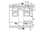
図1には、本実施の形態における炭化珪素半導体装置(縦型JFET)の縦断面図を示す。
図1において、SiCよりなるN+型ドレイン用基板1の上に、SiCよりなるN-型のドリフト層2と、SiCよりなるN+型のソース層3とが順に形成されている。また、ソース層3を貫通してドリフト層2に達するトレンチ4が形成されている。さらに、トレンチ4の内部にポリシリコンゲート電極5が配置されている。
【0021】
トレンチ4の内壁面には酸化膜(SiO2膜)6が形成されている。このように、トレンチ4の内壁面に酸化膜6を形成したことにより、ゲートリークに対して大きなバリアになり、ターンオン、オフ特性に影響を与えることができる。
【0022】
また、酸化膜6の外周側に半絶縁領域7が形成されている。半絶縁領域7はバナジウムイオンを拡散したもの(バナジウムイオン拡散領域)である。トレンチ底面におけるバナジウムイオン拡散領域7bの厚さは、トレンチ側面でのバナジウムイオン拡散領域7aの厚さよりも厚くなっている。ここで、酸化膜6中では電界強度がSiC中に比べて3倍になるので、酸化膜6に大きな電界がかかるが、酸化膜6の外周側に形成したバナジウムイオン拡散領域(半絶縁領域)7により電界を分担し緩和することができ、耐圧を向上させることができる。また、デバイスがオン状態のとき、トレンチ間で蓄積型のチャネルが形成でき、低オン抵抗化が可能となる。さらに、半絶縁領域7はトレンチ底面における半絶縁領域7bがトレンチ側面での半絶縁領域7aよりも厚くなっており、これにより、ドレイン電極とゲート電極間の高耐圧化がさらに可能となる。図1の構成はノーマリーオフとする場合に特に適している。
【0023】
また、ソース層3の上面にはソース電極8が形成されている。基板1の裏面(下面)にはドレイン電極9が形成されている。トレンチ4の内部のポリシリコンゲート電極5の上面におけるソース電極8との間には酸化膜10が形成されている。これにより、ゲート電極5とソース電極8とが電気的に分離されている。
【0024】
次に、炭化珪素半導体装置の製造方法について説明する。
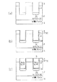
図2,3は製造工程の説明のための縦断面図である。
まず、図2(a)に示すように、N+型SiC基板1を用意し、エピタキシャル成長法により、その上にN-ドリフト層2とN+ソース層3を連続して形成する。このように、基板1上にN-ドリフト層2とN+ソース層3とを順に形成する。そして、図2(b)に示すように、ソース層3を貫通してドリフト層2に達するトレンチ4を形成する。これにはRIE法を用いる。
【0025】
その後、図2(c)に示すように、トレンチ4の内壁面(側面と底面)にバナジウムをイオン注入する。このとき、トレンチ底面に対しては垂直方向から強いエネルギーにてイオンを注入するとともに、トレンチ側面に対しては斜め方向から弱いエネルギーにてイオンを注入する。これにより、トレンチ底面におけるバナジウムイオン拡散領域7bは、トレンチ側面でのバナジウムイオン拡散領域7aよりも厚くなる。
【0026】
さらに、図3(a)に示すように、トレンチ4内の壁面に熱酸化膜(SiO2膜)6を形成する。このとき、バナジウムイオンの拡散領域7の表面に熱酸化膜を形成することになり、膜厚の厚い熱酸化膜を形成することができる(広義には、イオン拡散層の表面に熱酸化膜を形成することにより厚い膜厚を形成することができる)。
【0027】
このように、トレンチ4の内壁面に酸化膜6が、また、当該酸化膜6の外周側にバナジウムイオン拡散領域(半絶縁領域)7が位置するように、当該膜6および領域7を形成する。
【0028】
そして、図3(b)に示すように、ポリシリコン膜5をトレンチ4内が埋め込まれるように成膜し、さらに、エッチバックしてソース層3の上面のポリシリコン膜5を取り除く。このようにして、トレンチ4の内部にゲート電極となるポリシリコン膜5を埋め込む。
【0029】
さらに、図3(c)に示すように、800℃程度の熱酸化によりトレンチ4の内部のポリシリコン膜5の表面を熱酸化膜10で覆う。このとき、ポリシリコンは酸化温度が低く、SiCは酸化温度が高いので、当該熱酸化をポリシリコンの酸化温度とSiCの酸化温度との中間温度で行うようにする。このようにすると、セルフアラインでトレンチ開口部を塞ぐ酸化膜10を形成することができる。つまり、トレンチ4内においてポリシリコン膜5が露出するとともにソース層3の上面が露出する状態でポリシリコンが酸化する温度とSiCが酸化する温度の間の温度にて熱酸化を行うとポリシリコン膜5の上面に自己整合的に熱酸化膜10を形成することができる。よって、アイソレーションがセルフアラインで形成することができるようになる。従って、セルサイズを微細化する場合に有利である。
【0030】
その後、図1に示すように、熱酸化膜10上を含めたソース層3の上に金属膜を形成してソース電極8とするとともに、基板1の裏面に金属膜を形成してドレイン電極9とする。
【0031】
図1においてはトレンチ4の内壁面に酸化膜6を形成するとともに、酸化膜6の外周側に半絶縁領域7を形成し、この領域7はトレンチ底面における半絶縁領域7bはトレンチ側面での半絶縁領域7aよりも厚くしたが、図4に示すように、トレンチ底面において半絶縁領域を厚くする代わりにアルミニウムイオンを拡散した領域11を形成してもよい。詳しくは、例えばアルミニウムをイオン注入した後、バナジウムをイオン注入することにより作製することができる。このようにして、アルミニウムを拡散すると、即ち、トレンチ4底面における半絶縁領域7の下にSiCよりなるP型の不純物拡散領域11を形成すると、このP型の不純物拡散領域11とドリフト層2の間のビルトインポテンシャルの差を利用してドリフト層2へ空乏層を伸ばすことができるため、よりよくノーマリーオフが実現できる。
【0032】
また、図1の構成に対し図5に示すように、トレンチ側面および底面において酸化膜6の外周側に均等な厚さの半絶縁領域(バナジウムイオン拡散領域)7を形成してもよい。特にノーマリオンタイプにする場合に好ましい。
【0033】
なお、図1でのトレンチ4内の酸化膜6を無くし図6のようにすることも可能であり、さらに、トレンチ4の内部に埋め込むポリシリコンゲート電極5に関して、その導電型は、図6に示すようにP型であっても図7に示すようにN型であってもよい。特に図6の構成はノーマリオフタイプにする場合に好ましい。P型では、P型のポリシリコンとSiCの間の静電ポテンシャルの差が大きくなり、N-ドリフト側に空乏層を大きく伸ばすことが可能であるからである。
(第2の実施の形態)
次に、第2の実施の形態を、第1の実施の形態との相違点を中心に説明する。
【0034】
図8には、本実施の形態における炭化珪素半導体装置の縦断面図を示す。
図8において、トレンチ4の内壁面には酸化膜6が形成されている。また、図1でのバナジウムイオン拡散領域7の代わりに図8においては、酸化膜6の外周側にはSiCよりなるP+型のエピタキシャル膜20が形成されている。よって、トレンチ4の内壁面に酸化膜6を形成したことにより、ゲートリークに対して大きなバリアになり、ターンオン、オフ特性に影響を与えることができる。ここで、酸化膜中では電界強度がSiC中に比べて3倍になるので、酸化膜6に大きな電界がかかるが、酸化膜6の外周側に形成したP+型エピタキシャル膜20により電界を分担し緩和することができ、耐圧を向上させることができる。また、デバイスがオン状態のとき、トレンチ間で蓄積型のチャネルが形成でき、低オン抵抗化が可能となる。
【0035】
さらに、トレンチ4底面におけるエピタキシャル膜20の下には半絶縁領域21が形成されている。半絶縁領域21は、バナジウムイオンを拡散したもの(バナジウムイオン拡散領域)である。このように、トレンチ4の底部にバナジウムを拡散すると、高耐圧化がさらに可能である。
【0036】
また、トレンチ4内のポリシリコンゲート電極5およびP+型エピタキシャル膜20の上面におけるソース電極8との間には酸化膜22が形成されている。
次に、炭化珪素半導体装置の製造方法について説明する。
【0037】
図9,10は製造工程の説明のための縦断面図である。
まず、図2(a),(b)を用いて説明したように、N+型SiC基板1の上にエピタキシャル成長法によりN-ドリフト層2とN+ソース層3とを順に形成する。さらに、RIE法によりソース層3を貫通してドリフト層2に達するトレンチ4を形成する。
【0038】
その後、図9(a)に示すように、トレンチ4の底面にバナジウムをイオン注入してバナジウムイオン拡散領域21を形成する。
さらに、図9(b)に示すように、トレンチ4内の壁面にSiCよりなるP+型のエピタキシャル膜20を形成する。詳しくは、トレンチ4内を含めたソース層3の上面にP+エピ層20を形成し、さらに、ソース層3の上面のエピ膜20をエッチバックにより除去する。そして、図9(c)に示すように、エピタキシャル膜20の内面、即ち、トレンチ4内の壁面に熱酸化膜(SiO2膜)6を形成する。
【0039】
このように、トレンチ4の内壁面に酸化膜6が、また、当該酸化膜6の外周側にSiCよりなるP+型のエピタキシャル膜20が位置するように、当該両膜6,20を形成する。つまり、トレンチ4の内壁面にSiCよりなるP+型のエピタキシャル膜20が位置するように、また、当該エピタキシャル膜20の内側に酸化膜6が位置するように、当該両膜6,20を形成する。
【0040】
そして、図10(a)に示すように、ポリシリコン膜5をトレンチ4内が埋め込まれるように成膜し、さらに、エッチバックしてソース層3の上面のポリシリコン膜5を取り除く。このように、トレンチ4の内部にゲート電極となるポリシリコン膜5を埋め込む。
【0041】
さらに、図10(b)に示すように、800℃程度の熱酸化によりトレンチ4の内部のポリシリコン膜5の表面を熱酸化膜22aで覆う。さらに、図10(c)に示すように、LDD法によりエピ層20の上も酸化膜22bで覆う。つまり、基板上(ソース層3上)にLTO膜を全面に形成するとともにこのLTO膜に対し異方性エッチングを行い(エッチバックし)、熱酸化膜22aにサイドウォールを残すことによりエピ膜20の上を酸化膜22bで覆うようにする。このようにして、トレンチ4内においてポリシリコン膜5が露出するとともにソース層3の上面が露出する状態でポリシリコンが酸化する温度とSiCが酸化する温度の間の温度にて熱酸化を行いポリシリコン膜5の上面に自己整合的に熱酸化膜22aを形成し、さらに、P型のエピタキシャル膜20上を覆うように、LDD法により熱酸化膜22aに対し酸化膜によるサイドウォール22bを形成する。よって、アイソレーションがセルフアラインで形成することができるようになる。
【0042】
その後、図8に示すように、酸化膜22(22a,22b)の上を含めたソース層3の上に金属膜を形成してソース電極8とするとともに、基板1の裏面に金属膜を形成してドレイン電極9とする。
【0043】
図8においてはトレンチ4の内壁面に酸化膜6を形成するとともに、酸化膜6の外周側にP+型SiC膜20を形成し、トレンチ底面における膜20の下にバナジウムイオン拡散領域21を形成したが、図11に示すように、トレンチ底面における膜20の下にアルミニウムイオン拡散領域23を形成してもよい。このようにアルミニウムを拡散すると、即ち、トレンチ4底面におけるエピタキシャル膜20の下にSiCよりなるP型の不純物拡散領域23を形成すると、このP型の不純物拡散領域23とドリフト層の間のビルトインポテンシャルの差を利用してドリフト層へ空乏層を伸ばすことができるため、よりよくノーマリーオフが実現できる。
【0044】
また、図8の構成に対し図12に示すように、トレンチ底面においてバナジウムイオン拡散領域21を設けなくしてもよい。
なお、P型エピ膜20ではなく、図13に示すように、イオン注入または熱拡散によるP型不純物拡散領域24とすることも可能である。具体的には、例えばアルミやボロンやカーボンのイオン注入または熱拡散により形成する。
【0045】
また、トレンチ4の内部に埋め込むポリシリコンゲート電極5に関して、その導電型は、P型であってもN型であってもよい。
(第3の実施の形態)
次に、第3の実施の形態を、第1,2の実施の形態との相違点を中心に説明する。
【0046】
図14には、本実施の形態における炭化珪素半導体装置の縦断面図を示す。
第2実施形態での図8の酸化膜6が無く、図14において、トレンチ4の内壁面にSiCよりなるP+型のエピタキシャル膜30が形成されている。つまり、ポリシリコンゲート電極5とP+型エピタキシャル膜30との界面が形成されている。よって、ポリシリコンゲート電極5とP+エピ膜30の間のショットキーバリアによりリークを抑えることができる。また、蓄積チャネルは形成されないが、この構造については以下のメリットがある。隣り合うトレンチ間での側面における空乏層の広がりをコントロールすることにより電流制御ができ、オフ特性を得るためにトレンチ側面を有効に利用することができるため深いトレンチを形成する必要がなくなる。そのため、深いトレンチ4内にSiCのエピ層成長を行う必要がなくプロセスが容易となる。また、トレンチ深さを浅くでき、これにより、低オン抵抗化を図ることができる。このようにして、電界を緩和することができ、耐圧を向上させることができる。
【0047】
また、トレンチ4底面におけるエピタキシャル膜30の下に半絶縁領域31が形成されている。半絶縁領域31はバナジウムイオンを拡散したもの(バナジウムイオン拡散領域)である。さらに、トレンチ4内のゲート電極5およびP+型エピタキシャル膜30の上面におけるソース電極8との間には酸化膜22が形成されている。
【0048】
製造工程としては、トレンチ4を形成した後において、トレンチ4の底面にバナジウムイオン拡散領域31を形成し(図9(a)参照)、トレンチ4の内壁面にP+型エピタキシャル膜30を形成すればよい。その後は、図10(a)〜(c)のごとく、トレンチ4の内部にゲート電極となるポリシリコン膜5を埋め込み、トレンチ4内においてポリシリコン膜5が露出するとともにソース層3の上面が露出する状態でポリシリコンが酸化する温度とSiCが酸化する温度の間の温度にて熱酸化を行いポリシリコン膜5の上面に自己整合的に熱酸化膜22aを形成する。よって、アイソレーションがセルフアラインで形成することができるようになる。さらに、P型エピタキシャル膜30上を覆うように、LDD法により熱酸化膜22aに対し酸化膜によるサイドウォール22bを形成する。そして、酸化膜22a,22b上を含めたソース層3の上にソース電極8を形成する。
【0049】
図14に代わる構成を以下、説明する。
バナジウムイオン拡散領域31の代わりに、図15に示すように、トレンチ底面におけるエピタキシャル膜30の下にアルミニウムイオン拡散領域(SiCよりなるP型の不純物拡散領域)32を形成してもよい。
【0050】
図16に示すように、図14でのバナジウムイオン拡散領域31を無くしてもよい。
なお、P型エピ膜30ではなく、図17に示すようにイオン注入または熱拡散による不純物拡散領域33とすることも可能である。具体的には、例えば、アルミニウムやボロンやカーボンのイオン注入または熱拡散により形成する。
【0051】
また、トレンチ4の内部に埋め込むポリシリコンゲート電極5に関して、その導電型は、P型であってもN型であってもよい。
(第4の実施の形態)
次に、第4の実施の形態を、第3の実施の形態との相違点を中心に説明する。
【0052】
図18には、本実施の形態における炭化珪素半導体装置の縦断面図を示す。
図14に比べ図18においては、ポリシリコンゲート電極5への金属原子の拡散領域40にてゲート電極5とP+型エピタキシャル膜30との間にオーミックコンタクトをとっている。オーミックコンタクトによってデバイスのダイナミック特性が向上する。また、図14の酸化膜22に代わり、図18ではLTO膜43を形成している。
【0053】
次に、炭化珪素半導体装置の製造方法について説明する。
図19,20は製造工程の説明のための縦断面図である。
まず、図2(a),(b)を用いて説明したように、N+型SiC基板1の上にエピタキシャル成長法によりN-ドリフト層2とN+ソース層3とを順に形成する。さらに、RIE法によりソース層3を貫通してドリフト層2に達するトレンチ4を形成する。
【0054】
その後、図19(a)に示すように、トレンチ4の底面にバナジウムをイオン注入してバナジウムイオン拡散領域31を形成する。さらに、図19(b)に示すように、トレンチ4内の壁面にSiCよりなるP+型のエピタキシャル膜30を形成する。詳しくは、トレンチ4内を含めたソース層3の上面にP+エピ層30を形成し、さらに、ソース層3の上面のエピ膜30をエッチバックにより除去する。
【0055】
そして、図19(c)に示すように、トレンチ4の内部にゲート電極となるポリシリコン膜5をトレンチ4内が埋め込まれるように成膜し、さらに、エッチバックしてソース層3の上面のポリシリコン膜5を取り除く。
【0056】
さらに、図20(a)に示すように、ポリシリコン膜5の上面における中央部分に、金属膜としてのアルミ膜41とニッケル膜42の積層体を配置する。さらに、アニールを行って金属(41,42)をポリシリコン膜5内に拡散させる。これにより、ポリシリコンゲート電極5内においてP+型エピ膜30に達する金属原子の拡散領域40が形成される。つまり、アニールを行ってポリシリコン膜5とP+型エピタキシャル膜30との界面に達する金属原子の拡散領域40を形成する。その結果、ポリシリコンゲート電極5はP+型エピ膜30に対しオーミックコンタクトがとられる。
【0057】
その後、図20(b)に示すように、LTO膜43を成膜し、ソースコンタクト部を開口する。つまり、トレンチ4の内部のポリシリコン膜5およびP+型エピ膜30の上面をLTO膜43で覆う。さらに、図18に示すように、ソース層3の上面に金属膜を形成してソース電極8とするとともに、基板1の裏面に金属膜を形成してドレイン電極9とする。
【0058】
金属原子の拡散領域40を形成するための原子源としての金属膜41,42をゲート配線材として用いることができる。
本実施形態の応用例として、バナジウムイオン拡散領域31の代わりに図21に示すように、アルミニウムイオン拡散領域44を形成してもよい。また、図22に示すように、トレンチ底部に拡散領域を設けないようにしてもよい。
【0059】
なお、P型エピ膜30ではなく、図23に示すように、イオン注入または熱拡散によるP型不純物拡散領域45とすることも可能である。具体的には、例えば、アルミやボロンやカーボンのイオン注入または熱拡散により形成する。
【0060】
また、トレンチ4の内部に埋め込むポリシリコンゲート電極5に関して、その導電型は、P型であってもN型であってもよい。
【図面の簡単な説明】
【図1】第1の実施の形態における炭化珪素半導体装置の縦断面図。
【図2】炭化珪素半導体装置の製造工程を説明するための縦断面図。
【図3】炭化珪素半導体装置の製造工程を説明するための縦断面図。
【図4】別例の炭化珪素半導体装置の縦断面図。
【図5】別例の炭化珪素半導体装置の縦断面図。
【図6】別例の炭化珪素半導体装置の縦断面図。
【図7】別例の炭化珪素半導体装置の縦断面図。
【図8】第2の実施の形態における炭化珪素半導体装置の縦断面図。
【図9】炭化珪素半導体装置の製造工程を説明するための縦断面図。
【図10】炭化珪素半導体装置の製造工程を説明するための縦断面図。
【図11】別例の炭化珪素半導体装置の縦断面図。
【図12】別例の炭化珪素半導体装置の縦断面図。
【図13】別例の炭化珪素半導体装置の縦断面図。
【図14】第3の実施の形態における炭化珪素半導体装置の縦断面図。
【図15】別例の炭化珪素半導体装置の縦断面図。
【図16】別例の炭化珪素半導体装置の縦断面図。
【図17】別例の炭化珪素半導体装置の縦断面図。
【図18】第4の実施の形態における炭化珪素半導体装置の縦断面図。
【図19】炭化珪素半導体装置の製造工程を説明するための縦断面図。
【図20】炭化珪素半導体装置の製造工程を説明するための縦断面図。
【図21】別例の炭化珪素半導体装置の縦断面図。
【図22】別例の炭化珪素半導体装置の縦断面図。
【図23】別例の炭化珪素半導体装置の縦断面図。
【図24】従来技術を説明するための炭化珪素半導体装置の縦断面図。
【符号の説明】
1…N+型ドレイン用基板、2…N-型ドリフト層、3…N+型ソース層3、4…トレンチ、5…ポリシリコンゲート電極、6…酸化膜、7…バナジウムイオン拡散領域、7a…バナジウムイオン拡散領域、7b…バナジウムイオン拡散領域、8…ソース電極、9…ドレイン電極、10…酸化膜、20…P+型エピタキシャル膜、22…酸化膜、30…P+型エピタキシャル膜、31…バナジウムイオン拡散領域、32…アルミニウムイオン拡散領域、40…金属原子拡散領域。[0001]
BACKGROUND OF THE INVENTION
The present invention relates to a silicon carbide semiconductor device, and more particularly to a vertical junction FET (vertical JFET).
[0002]
[Prior art]
A vertical JFET using SiC as a material is disclosed in Technical Digest of Int'l Contf. On SiC and Related Materials-ICS CRM2001-, Tsukuba, Japan, 2001 p327. This is shown in FIG. On the N +
[0003]
However, since the electric field strength in the
[0004]
[Problems to be solved by the invention]
The present invention has been made under such a background, and an object of the present invention is to provide a silicon carbide semiconductor device capable of reducing the electric field and improving the breakdown voltage.
[0005]
[Means for Solving the Problems]
2. The silicon carbide semiconductor device according to
Here, since the electric field strength in the oxide film is three times that in SiC, a large electric field is applied to the oxide film, but the electric field is shared by the semi-insulating region formed by injecting vanadium ions into the drift layer and the source layer. Can be relaxed and the breakdown voltage can be improved. Further, when the device is in an on state, a storage type channel can be formed between the trenches, and a low on-resistance can be achieved.
[0006]
As described in
[0007]
Further, as described in
[0008]
6. The silicon carbide semiconductor device according to
[0009]
According to a sixth aspect of the present invention , a semi-insulating region formed by implanting vanadium ions into the drift layer or an impurity diffusion region of the second conductivity type made of SiC may be formed below the epitaxial film at the bottom of the trench . In particular, when forming a semi-insulating region at the bottom of the trench, a high breakdown voltage is further possible. In addition, when the second conductivity type impurity diffusion region made of SiC is formed, normally-off can be better realized.
[0010]
As described in
[0015]
The silicon carbide semiconductor device according to
[0016]
The silicon carbide semiconductor device according to
[0019]
DETAILED DESCRIPTION OF THE INVENTION
(First embodiment)
Hereinafter, a first embodiment of the present invention will be described with reference to the drawings.
[0020]
FIG. 1 is a longitudinal sectional view of a silicon carbide semiconductor device (vertical JFET) in the present embodiment.
In FIG. 1, an N −
[0021]
An oxide film (SiO 2 film) 6 is formed on the inner wall surface of the
[0022]
A
[0023]
A
[0024]
Next, a method for manufacturing the silicon carbide semiconductor device will be described.
2 and 3 are longitudinal sectional views for explaining the manufacturing process.
First, as shown in FIG. 2A, an N +
[0025]
Thereafter, as shown in FIG. 2C, vanadium is ion-implanted into the inner wall surface (side surface and bottom surface) of the
[0026]
Further, as shown in FIG. 3A, a thermal oxide film (SiO 2 film) 6 is formed on the wall surface in the
[0027]
Thus, the
[0028]
Then, as shown in FIG. 3B, a
[0029]
Further, as shown in FIG. 3C, the surface of the
[0030]
Thereafter, as shown in FIG. 1, a metal film is formed on the
[0031]
In FIG. 1, an
[0032]
1, semi-insulating regions (vanadium ion diffusion regions) 7 having a uniform thickness may be formed on the outer peripheral side of the
[0033]
It is possible to eliminate the
(Second Embodiment)
Next, the second embodiment will be described focusing on the differences from the first embodiment.
[0034]
FIG. 8 shows a longitudinal sectional view of the silicon carbide semiconductor device in the present embodiment.
In FIG. 8, an
[0035]
Further, a
[0036]
An
Next, a method for manufacturing the silicon carbide semiconductor device will be described.
[0037]
9 and 10 are longitudinal sectional views for explaining the manufacturing process.
First, as described with reference to FIGS. 2A and 2B, the N − drift layer 2 and the N + source layer 3 are sequentially formed on the N +
[0038]
Thereafter, as shown in FIG. 9A, vanadium ions are implanted into the bottom surface of the
Further, as shown in FIG. 9B, a P +
[0039]
In this way, the
[0040]
Then, as shown in FIG. 10A, a
[0041]
Further, as shown in FIG. 10B, the surface of the
[0042]
Thereafter, as shown in FIG. 8, a metal film is formed on the
[0043]
In FIG. 8, an
[0044]
Further, the vanadium
Instead of the P-
[0045]
The conductivity type of the
(Third embodiment)
Next, the third embodiment will be described focusing on the differences from the first and second embodiments.
[0046]
FIG. 14 is a longitudinal sectional view of the silicon carbide semiconductor device in the present embodiment.
There is no
[0047]
A
[0048]
As a manufacturing process, after the
[0049]
A configuration alternative to FIG. 14 will be described below.
Instead of the vanadium
[0050]
As shown in FIG. 16, the vanadium
Instead of the P-
[0051]
The conductivity type of the
(Fourth embodiment)
Next, the fourth embodiment will be described focusing on the differences from the third embodiment.
[0052]
FIG. 18 is a longitudinal sectional view of the silicon carbide semiconductor device in the present embodiment.
Compared to FIG. 14, in FIG. 18, an ohmic contact is made between the
[0053]
Next, a method for manufacturing the silicon carbide semiconductor device will be described.
19 and 20 are longitudinal sectional views for explaining the manufacturing process.
First, as described with reference to FIGS. 2A and 2B, the N − drift layer 2 and the N + source layer 3 are sequentially formed on the N +
[0054]
Thereafter, as shown in FIG. 19A, vanadium ions are implanted into the bottom surface of the
[0055]
Then, as shown in FIG. 19C, a
[0056]
Further, as shown in FIG. 20A, a laminated body of an
[0057]
Thereafter, as shown in FIG. 20B, an
[0058]
As an application example of this embodiment, an aluminum
[0059]
Instead of the P-
[0060]
The conductivity type of the
[Brief description of the drawings]
FIG. 1 is a longitudinal sectional view of a silicon carbide semiconductor device according to a first embodiment.
FIG. 2 is a longitudinal sectional view for illustrating a process for manufacturing a silicon carbide semiconductor device.
FIG. 3 is a longitudinal sectional view for illustrating a process for manufacturing a silicon carbide semiconductor device.
FIG. 4 is a longitudinal sectional view of another example silicon carbide semiconductor device.
FIG. 5 is a longitudinal sectional view of another example of a silicon carbide semiconductor device.
FIG. 6 is a longitudinal sectional view of another example of a silicon carbide semiconductor device.
FIG. 7 is a longitudinal sectional view of another example of a silicon carbide semiconductor device.
FIG. 8 is a longitudinal sectional view of a silicon carbide semiconductor device in a second embodiment.
FIG. 9 is a longitudinal sectional view for illustrating the manufacturing process for the silicon carbide semiconductor device.
FIG. 10 is a longitudinal sectional view for illustrating a process for manufacturing a silicon carbide semiconductor device.
FIG. 11 is a longitudinal sectional view of another example silicon carbide semiconductor device.
FIG. 12 is a longitudinal sectional view of another example of a silicon carbide semiconductor device.
FIG. 13 is a longitudinal sectional view of another example of a silicon carbide semiconductor device.
FIG. 14 is a longitudinal sectional view of a silicon carbide semiconductor device in a third embodiment.
FIG. 15 is a longitudinal sectional view of another example of a silicon carbide semiconductor device.
FIG. 16 is a longitudinal sectional view of another example of a silicon carbide semiconductor device.
FIG. 17 is a longitudinal sectional view of another example silicon carbide semiconductor device.
FIG. 18 is a longitudinal sectional view of a silicon carbide semiconductor device in a fourth embodiment.
FIG. 19 is a longitudinal sectional view for illustrating the manufacturing process for the silicon carbide semiconductor device.
FIG. 20 is a longitudinal sectional view for illustrating the manufacturing process for the silicon carbide semiconductor device.
FIG. 21 is a longitudinal sectional view of another example of a silicon carbide semiconductor device.
FIG. 22 is a longitudinal sectional view of another example of a silicon carbide semiconductor device.
FIG. 23 is a longitudinal sectional view of another example of a silicon carbide semiconductor device.
FIG. 24 is a longitudinal sectional view of a silicon carbide semiconductor device for illustrating a conventional technique.
[Explanation of symbols]
1 ... N + -type drain substrate, 2 ... N - -type drift layer, 3 ... N + -type source layers 3, 4 ... trench, 5 ... polysilicon gate electrode, 6 ... oxide film, 7 ... vanadium ion diffusion region, 7a ... Vanadium ion diffusion region, 7b ... Vanadium ion diffusion region, 8 ... Source electrode, 9 ... Drain electrode, 10 ... Oxide film, 20 ... P + type epitaxial film, 22 ... Oxide film, 30 ... P + type epitaxial film, 31 ... Vanadium ion diffusion region, 32 ... Aluminum ion diffusion region, 40 ... Metal atom diffusion region.
Claims (9)
前記ドリフト層(2)及び前記ソース層(3)のうち前記トレンチ(4)の内壁面を構成する部分にはバナジウムイオンが注入されて半絶縁領域(7)が形成されているとともに、前記半絶縁領域(7)の表面には酸化膜(6)が形成されていることを特徴とする炭化珪素半導体装置。On the first conductivity type drain substrate (1) made of SiC, a low-concentration first conductivity type drift layer (2) made of SiC and a high-concentration first conductivity type source layer made of SiC ( with 3) and are formed in this order, a trench reaching said source layer (3) drift layer through the (2) (4) is formed, further, a gate electrode (5 inside the trench (4) ) Is a silicon carbide semiconductor device,
A portion of the drift layer (2) and the source layer (3) constituting the inner wall surface of the trench (4) is implanted with vanadium ions to form a semi-insulating region (7). A silicon carbide semiconductor device, wherein an oxide film (6) is formed on a surface of the insulating region (7) .
前記トレンチ(4)の内壁面には、第2導電型のエピタキシャル膜(20)が形成されているとともに、前記第2導電型のエピタキシャル膜(20)の表面には、酸化膜(6)が形成されていることを特徴とする炭化珪素半導体装置。 On the first conductivity type drain substrate (1) made of SiC, a low-concentration first conductivity type drift layer (2) made of SiC and a high-concentration first conductivity type source layer made of SiC ( 3) are formed in order, and a trench (4) that penetrates the source layer (3) and reaches the drift layer (2) is formed. Further, a gate electrode (5) is formed inside the trench (4). ) Is a silicon carbide semiconductor device,
A second conductivity type epitaxial film (20) is formed on the inner wall surface of the trench (4), and an oxide film (6) is formed on the surface of the second conductivity type epitaxial film (20). carbonization silicon semiconductor device you characterized in that it is formed.
SiCよりなる第1導電型のドレイン用基板(1)の上に、SiCよりなる低濃度な第1導電型のドリフト層(2)と、SiCよりなる高濃度な第1導電型のソース層(3)とを順に形成する工程と、
前記ソース層(3)を貫通してドリフト層(2)に達するトレンチ(4)を形成する工程と、
前記トレンチ(4)の内壁面にバナジウムイオンを注入して半絶縁領域(7)を形成する工程と、
前記半絶縁領域(7)の表面に酸化膜(6)形成する工程と、
前記トレンチ(4)の内部にゲート電極となるポリシリコン膜(5)を埋め込む工程と、
前記トレンチ(4)内においてポリシリコン膜(5)が露出するとともに前記ソース層 (3)の上面が露出する状態でポリシリコンが酸化する温度とSiCが酸化する温度の間の温度にて熱酸化を行いポリシリコン膜(5)の上面に自己整合的に熱酸化膜(10)を形成する工程と、
前記熱酸化膜(10)上を含めた前記ソース層(3)の上にソース電極(8)を形成する工程と、
を備えたことを特徴とする炭化珪素半導体装置の製造方法。 On the first conductivity type drain substrate (1) made of SiC, a low-concentration first conductivity type drift layer (2) made of SiC and a high-concentration first conductivity type source layer made of SiC ( 3) are formed in order, and a trench (4) that penetrates the source layer (3) and reaches the drift layer (2) is formed. Further, a gate electrode (5) is formed inside the trench (4). ) Is a method for manufacturing a silicon carbide semiconductor device,
On the first conductivity type drain substrate (1) made of SiC, a low-concentration first conductivity type drift layer (2) made of SiC and a high-concentration first conductivity type source layer made of SiC ( And 3) in order,
Forming a trench (4) that penetrates the source layer (3) and reaches the drift layer (2);
Injecting vanadium ions into the inner wall of the trench (4) to form a semi-insulating region (7);
Forming an oxide film (6) on the surface of the semi-insulating region (7);
Burying a polysilicon film (5) to be a gate electrode inside the trench (4);
Thermal oxidation is performed at a temperature between the temperature at which polysilicon is oxidized and the temperature at which SiC is oxidized with the polysilicon film (5) exposed in the trench (4) and the upper surface of the source layer (3) exposed. Forming a thermal oxide film (10) in a self-aligned manner on the upper surface of the polysilicon film (5);
Forming a source electrode (8) on the source layer (3) including the thermal oxide film (10);
Method for producing a carbonization silicon semiconductor device you comprising the.
SiCよりなる第1導電型のドレイン用基板(1)の上に、SiCよりなる低濃度な第1導電型のドリフト層(2)と、SiCよりなる高濃度な第1導電型のソース層(3)とを順に形成する工程と、
前記ソース層(3)を貫通してドリフト層(2)に達するトレンチ(4)を形成する工程と、
前記トレンチ(4)の内壁面にSiCよりなる第2導電型のエピタキシャル膜(20)を形成する工程と、
前記第2導電型のエピタキシャル膜(20)の表面に酸化膜(6)を形成する工程と、
前記トレンチ(4)の内部にゲート電極となるポリシリコン膜(5)を埋め込む工程と、
前記トレンチ(4)内においてポリシリコン膜(5)が露出するとともに前記ソース層(3)の上面が露出する状態でポリシリコンが酸化する温度とSiCが酸化する温度の間の温度にて熱酸化を行いポリシリコン膜(5)の上面に自己整合的に熱酸化膜(22a)を形成する工程と、
前記ソース層(3)上の全面に酸化膜を形成するとともに該酸化膜に対して異方性エッチングを行って前記熱酸化膜にサイドウォールを残すことにより前記エピタキシャル膜(20)の上に酸化膜(22b)を形成する工程と、
前記酸化膜(22a、22b)上を含めた前記ソース層(3)の上にソース電極(8)を形成する工程と、
を備えたことを特徴とする炭化珪素半導体装置の製造方法。 On the first conductivity type drain substrate (1) made of SiC, a low-concentration first conductivity type drift layer (2) made of SiC and a high-concentration first conductivity type source layer made of SiC ( 3) are formed in order, and a trench (4) that penetrates the source layer (3) and reaches the drift layer (2) is formed. Further, a gate electrode (5) is formed inside the trench (4). ) Is a method for manufacturing a silicon carbide semiconductor device,
On the first conductivity type drain substrate (1) made of SiC, a low-concentration first conductivity type drift layer (2) made of SiC and a high-concentration first conductivity type source layer made of SiC ( And 3) in order,
Forming a trench (4) that penetrates the source layer (3) and reaches the drift layer (2);
Forming a second conductivity type epitaxial film (20) made of SiC on the inner wall surface of the trench (4);
Forming an oxide film (6) on the surface of the second conductivity type epitaxial film (20);
Burying a polysilicon film (5) to be a gate electrode inside the trench (4);
Thermal oxidation is performed at a temperature between the temperature at which polysilicon is oxidized and the temperature at which SiC is oxidized with the polysilicon film (5) exposed in the trench (4) and the upper surface of the source layer (3) exposed. Performing a self-aligned thermal oxide film (22a) on the upper surface of the polysilicon film (5),
An oxide film is formed on the entire surface of the source layer (3) and anisotropic etching is performed on the oxide film to leave sidewalls on the thermal oxide film, thereby oxidizing the epitaxial film (20). Forming a film (22b);
Forming a source electrode (8) on the source layer (3) including the oxide films (22a, 22b);
Method for producing a carbonization silicon semiconductor device you comprising the.
Priority Applications (1)
| Application Number | Priority Date | Filing Date | Title |
|---|---|---|---|
| JP2002023306A JP4096569B2 (en) | 2002-01-31 | 2002-01-31 | Silicon carbide semiconductor device and manufacturing method thereof |
Applications Claiming Priority (1)
| Application Number | Priority Date | Filing Date | Title |
|---|---|---|---|
| JP2002023306A JP4096569B2 (en) | 2002-01-31 | 2002-01-31 | Silicon carbide semiconductor device and manufacturing method thereof |
Related Child Applications (1)
| Application Number | Title | Priority Date | Filing Date |
|---|---|---|---|
| JP2007310739A Division JP4900212B2 (en) | 2007-11-30 | 2007-11-30 | Silicon carbide semiconductor device and manufacturing method thereof |
Publications (2)
| Publication Number | Publication Date |
|---|---|
| JP2003224277A JP2003224277A (en) | 2003-08-08 |
| JP4096569B2 true JP4096569B2 (en) | 2008-06-04 |
Family
ID=27746051
Family Applications (1)
| Application Number | Title | Priority Date | Filing Date |
|---|---|---|---|
| JP2002023306A Expired - Fee Related JP4096569B2 (en) | 2002-01-31 | 2002-01-31 | Silicon carbide semiconductor device and manufacturing method thereof |
Country Status (1)
| Country | Link |
|---|---|
| JP (1) | JP4096569B2 (en) |
Families Citing this family (15)
| Publication number | Priority date | Publication date | Assignee | Title |
|---|---|---|---|---|
| JP4564362B2 (en) * | 2004-01-23 | 2010-10-20 | 株式会社東芝 | Semiconductor device |
| JP4857527B2 (en) * | 2004-05-24 | 2012-01-18 | 株式会社デンソー | Method for manufacturing silicon carbide semiconductor device |
| JP4696471B2 (en) * | 2004-05-24 | 2011-06-08 | 株式会社デンソー | Silicon carbide semiconductor device and manufacturing method thereof |
| JP4046140B1 (en) | 2006-11-29 | 2008-02-13 | 住友電気工業株式会社 | Method for manufacturing silicon carbide semiconductor device |
| WO2008149799A1 (en) * | 2007-05-30 | 2008-12-11 | Rohm Co., Ltd. | Semiconductor device |
| WO2008149800A1 (en) * | 2007-05-30 | 2008-12-11 | Rohm Co., Ltd. | Semiconductor device |
| US8217419B2 (en) | 2007-06-15 | 2012-07-10 | Rohm Co., Ltd. | Semiconductor device |
| DE112009000535B4 (en) * | 2008-03-07 | 2013-08-01 | Mitsubishi Electric Corp. | Silicon carbide semiconductor device and method for its production |
| JP5621198B2 (en) * | 2009-03-04 | 2014-11-05 | 日産自動車株式会社 | Semiconductor device |
| US8823089B2 (en) * | 2011-04-15 | 2014-09-02 | Infineon Technologies Ag | SiC semiconductor power device |
| JP2015056492A (en) * | 2013-09-11 | 2015-03-23 | 株式会社東芝 | Semiconductor device |
| JP6237046B2 (en) * | 2013-09-25 | 2017-11-29 | 住友電気工業株式会社 | Silicon carbide semiconductor device and manufacturing method thereof |
| JP6337726B2 (en) | 2014-09-29 | 2018-06-06 | 株式会社デンソー | Semiconductor device and manufacturing method thereof |
| WO2018155566A1 (en) * | 2017-02-24 | 2018-08-30 | 三菱電機株式会社 | Silicon carbide semiconductor device, and electric power converting device |
| JP6750590B2 (en) * | 2017-09-27 | 2020-09-02 | 株式会社デンソー | Silicon carbide semiconductor device |
Family Cites Families (5)
| Publication number | Priority date | Publication date | Assignee | Title |
|---|---|---|---|---|
| JPS62174977A (en) * | 1985-09-30 | 1987-07-31 | Toshiba Corp | Thin-film static induction transistor and manufacture thereof |
| JP3189543B2 (en) * | 1993-12-22 | 2001-07-16 | 日産自動車株式会社 | Semiconductor device |
| JPH09172187A (en) * | 1995-12-19 | 1997-06-30 | Hitachi Ltd | Junction type field-effect semiconductor device and its manufacture |
| JP3848700B2 (en) * | 1996-05-10 | 2006-11-22 | 株式会社イオン工学研究所 | Silicon carbide semiconductor device |
| JP3575331B2 (en) * | 1999-05-17 | 2004-10-13 | 日産自動車株式会社 | Field effect transistor |
-
2002
- 2002-01-31 JP JP2002023306A patent/JP4096569B2/en not_active Expired - Fee Related
Also Published As
| Publication number | Publication date |
|---|---|
| JP2003224277A (en) | 2003-08-08 |
Similar Documents
| Publication | Publication Date | Title |
|---|---|---|
| JP4123636B2 (en) | Silicon carbide semiconductor device and manufacturing method thereof | |
| JP3959856B2 (en) | Silicon carbide semiconductor device and manufacturing method thereof | |
| JP4738562B2 (en) | Manufacturing method of semiconductor device | |
| JP2662217B2 (en) | Vertical gate semiconductor device and method of manufacturing the same | |
| JP4192281B2 (en) | Silicon carbide semiconductor device | |
| JP5586887B2 (en) | Semiconductor device and manufacturing method thereof | |
| US8174066B2 (en) | Semiconductor device and method of manufacturing semiconductor device | |
| KR100958421B1 (en) | Power device and manufacturing method thereof | |
| US9276067B2 (en) | SiC semiconductor device and manufacturing method thereof | |
| JP4096569B2 (en) | Silicon carbide semiconductor device and manufacturing method thereof | |
| JP4595144B2 (en) | Silicon carbide semiconductor device and manufacturing method thereof | |
| CN103477439B (en) | Semiconductor device and process for production thereof | |
| JP3575331B2 (en) | Field effect transistor | |
| JP2001284584A (en) | Semiconductor device and manufacturing method thereof | |
| JP2010021176A (en) | Semiconductor device and method of manufacturing the same | |
| US9853099B1 (en) | Double diffused metal oxide semiconductor device and manufacturing method thereof | |
| JPH1126758A (en) | Trench type MOS semiconductor device and method of manufacturing the same | |
| JP2003518748A (en) | Self-aligned silicon carbide LMOSFET | |
| JP2000269487A (en) | Semiconductor device and manufacturing method thereof | |
| JP2006019508A (en) | Semiconductor device and manufacturing method thereof | |
| JP2850852B2 (en) | Semiconductor device | |
| JP2001127285A (en) | Vertical field-effect transistor | |
| JP3642768B2 (en) | Horizontal high voltage semiconductor device | |
| JPH09129868A (en) | Semiconductor device and its manufacture | |
| JP4900212B2 (en) | Silicon carbide semiconductor device and manufacturing method thereof |
Legal Events
| Date | Code | Title | Description |
|---|---|---|---|
| A621 | Written request for application examination |
Free format text: JAPANESE INTERMEDIATE CODE: A621 Effective date: 20040413 |
|
| A977 | Report on retrieval |
Free format text: JAPANESE INTERMEDIATE CODE: A971007 Effective date: 20050912 |
|
| A131 | Notification of reasons for refusal |
Free format text: JAPANESE INTERMEDIATE CODE: A131 Effective date: 20071002 |
|
| A521 | Request for written amendment filed |
Free format text: JAPANESE INTERMEDIATE CODE: A523 Effective date: 20071130 |
|
| TRDD | Decision of grant or rejection written | ||
| A01 | Written decision to grant a patent or to grant a registration (utility model) |
Free format text: JAPANESE INTERMEDIATE CODE: A01 Effective date: 20080219 |
|
| A61 | First payment of annual fees (during grant procedure) |
Free format text: JAPANESE INTERMEDIATE CODE: A61 Effective date: 20080303 |
|
| R150 | Certificate of patent or registration of utility model |
Free format text: JAPANESE INTERMEDIATE CODE: R150 |
|
| FPAY | Renewal fee payment (event date is renewal date of database) |
Free format text: PAYMENT UNTIL: 20110321 Year of fee payment: 3 |
|
| FPAY | Renewal fee payment (event date is renewal date of database) |
Free format text: PAYMENT UNTIL: 20120321 Year of fee payment: 4 |
|
| FPAY | Renewal fee payment (event date is renewal date of database) |
Free format text: PAYMENT UNTIL: 20120321 Year of fee payment: 4 |
|
| FPAY | Renewal fee payment (event date is renewal date of database) |
Free format text: PAYMENT UNTIL: 20130321 Year of fee payment: 5 |
|
| FPAY | Renewal fee payment (event date is renewal date of database) |
Free format text: PAYMENT UNTIL: 20140321 Year of fee payment: 6 |
|
| R250 | Receipt of annual fees |
Free format text: JAPANESE INTERMEDIATE CODE: R250 |
|
| R250 | Receipt of annual fees |
Free format text: JAPANESE INTERMEDIATE CODE: R250 |
|
| R250 | Receipt of annual fees |
Free format text: JAPANESE INTERMEDIATE CODE: R250 |
|
| LAPS | Cancellation because of no payment of annual fees |