JP5586887B2 - Semiconductor device and manufacturing method thereof - Google Patents
Semiconductor device and manufacturing method thereof Download PDFInfo
- Publication number
- JP5586887B2 JP5586887B2 JP2009169693A JP2009169693A JP5586887B2 JP 5586887 B2 JP5586887 B2 JP 5586887B2 JP 2009169693 A JP2009169693 A JP 2009169693A JP 2009169693 A JP2009169693 A JP 2009169693A JP 5586887 B2 JP5586887 B2 JP 5586887B2
- Authority
- JP
- Japan
- Prior art keywords
- region
- body region
- semiconductor device
- width
- layer
- Prior art date
- Legal status (The legal status is an assumption and is not a legal conclusion. Google has not performed a legal analysis and makes no representation as to the accuracy of the status listed.)
- Expired - Fee Related
Links
Images


Classifications
-
- H—ELECTRICITY
- H10—SEMICONDUCTOR DEVICES; ELECTRIC SOLID-STATE DEVICES NOT OTHERWISE PROVIDED FOR
- H10D—INORGANIC ELECTRIC SEMICONDUCTOR DEVICES
- H10D30/00—Field-effect transistors [FET]
- H10D30/60—Insulated-gate field-effect transistors [IGFET]
- H10D30/64—Double-diffused metal-oxide semiconductor [DMOS] FETs
- H10D30/66—Vertical DMOS [VDMOS] FETs
- H10D30/668—Vertical DMOS [VDMOS] FETs having trench gate electrodes, e.g. UMOS transistors
-
- H—ELECTRICITY
- H10—SEMICONDUCTOR DEVICES; ELECTRIC SOLID-STATE DEVICES NOT OTHERWISE PROVIDED FOR
- H10D—INORGANIC ELECTRIC SEMICONDUCTOR DEVICES
- H10D12/00—Bipolar devices controlled by the field effect, e.g. insulated-gate bipolar transistors [IGBT]
- H10D12/01—Manufacture or treatment
- H10D12/031—Manufacture or treatment of IGBTs
-
- H—ELECTRICITY
- H10—SEMICONDUCTOR DEVICES; ELECTRIC SOLID-STATE DEVICES NOT OTHERWISE PROVIDED FOR
- H10D—INORGANIC ELECTRIC SEMICONDUCTOR DEVICES
- H10D30/00—Field-effect transistors [FET]
- H10D30/01—Manufacture or treatment
- H10D30/021—Manufacture or treatment of FETs having insulated gates [IGFET]
- H10D30/028—Manufacture or treatment of FETs having insulated gates [IGFET] of double-diffused metal oxide semiconductor [DMOS] FETs
- H10D30/0291—Manufacture or treatment of FETs having insulated gates [IGFET] of double-diffused metal oxide semiconductor [DMOS] FETs of vertical DMOS [VDMOS] FETs
- H10D30/0297—Manufacture or treatment of FETs having insulated gates [IGFET] of double-diffused metal oxide semiconductor [DMOS] FETs of vertical DMOS [VDMOS] FETs using recessing of the gate electrodes, e.g. to form trench gate electrodes
-
- H—ELECTRICITY
- H10—SEMICONDUCTOR DEVICES; ELECTRIC SOLID-STATE DEVICES NOT OTHERWISE PROVIDED FOR
- H10D—INORGANIC ELECTRIC SEMICONDUCTOR DEVICES
- H10D62/00—Semiconductor bodies, or regions thereof, of devices having potential barriers
- H10D62/10—Shapes, relative sizes or dispositions of the regions of the semiconductor bodies; Shapes of the semiconductor bodies
- H10D62/124—Shapes, relative sizes or dispositions of the regions of semiconductor bodies or of junctions between the regions
- H10D62/126—Top-view geometrical layouts of the regions or the junctions
- H10D62/127—Top-view geometrical layouts of the regions or the junctions of cellular field-effect devices, e.g. multicellular DMOS transistors or IGBTs
-
- H—ELECTRICITY
- H10—SEMICONDUCTOR DEVICES; ELECTRIC SOLID-STATE DEVICES NOT OTHERWISE PROVIDED FOR
- H10D—INORGANIC ELECTRIC SEMICONDUCTOR DEVICES
- H10D62/00—Semiconductor bodies, or regions thereof, of devices having potential barriers
- H10D62/10—Shapes, relative sizes or dispositions of the regions of the semiconductor bodies; Shapes of the semiconductor bodies
- H10D62/17—Semiconductor regions connected to electrodes not carrying current to be rectified, amplified or switched, e.g. channel regions
- H10D62/393—Body regions of DMOS transistors or IGBTs
-
- H—ELECTRICITY
- H10—SEMICONDUCTOR DEVICES; ELECTRIC SOLID-STATE DEVICES NOT OTHERWISE PROVIDED FOR
- H10D—INORGANIC ELECTRIC SEMICONDUCTOR DEVICES
- H10D62/00—Semiconductor bodies, or regions thereof, of devices having potential barriers
- H10D62/80—Semiconductor bodies, or regions thereof, of devices having potential barriers characterised by the materials
- H10D62/83—Semiconductor bodies, or regions thereof, of devices having potential barriers characterised by the materials being Group IV materials, e.g. B-doped Si or undoped Ge
- H10D62/832—Semiconductor bodies, or regions thereof, of devices having potential barriers characterised by the materials being Group IV materials, e.g. B-doped Si or undoped Ge being Group IV materials comprising two or more elements, e.g. SiGe
- H10D62/8325—Silicon carbide
-
- H—ELECTRICITY
- H10—SEMICONDUCTOR DEVICES; ELECTRIC SOLID-STATE DEVICES NOT OTHERWISE PROVIDED FOR
- H10D—INORGANIC ELECTRIC SEMICONDUCTOR DEVICES
- H10D62/00—Semiconductor bodies, or regions thereof, of devices having potential barriers
- H10D62/40—Crystalline structures
- H10D62/405—Orientations of crystalline planes
-
- H—ELECTRICITY
- H10—SEMICONDUCTOR DEVICES; ELECTRIC SOLID-STATE DEVICES NOT OTHERWISE PROVIDED FOR
- H10D—INORGANIC ELECTRIC SEMICONDUCTOR DEVICES
- H10D62/00—Semiconductor bodies, or regions thereof, of devices having potential barriers
- H10D62/80—Semiconductor bodies, or regions thereof, of devices having potential barriers characterised by the materials
- H10D62/85—Semiconductor bodies, or regions thereof, of devices having potential barriers characterised by the materials being Group III-V materials, e.g. GaAs
- H10D62/8503—Nitride Group III-V materials, e.g. AlN or GaN
Landscapes
- Electrodes Of Semiconductors (AREA)
Description
本発明は、UMOSFETを形成しても、耐圧を落とすことなく閾値電圧を下げることができるパワー半導体素子に関するものである。 The present invention relates to a power semiconductor element that can reduce a threshold voltage without lowering a breakdown voltage even when a UMOSFET is formed.
半導体パワー素子においてオン抵抗と耐圧は基板材料のバンドギャップで規定されるトレードオフの関係にある。そのため、パワー素子として広く用いられているシリコン素子の性能を超えるためには、シリコンよりもバンドギャップが大きな基板材料を用いることが有効である。特に、炭化珪素(SiC)は、シリコンに比べバンドギャップが約3倍と十分大きいこと、p型およびn型の導電型を容易に形成できること、熱酸化により酸化膜を形成できることなどの特長を有することから、高性能のMOSFET(Metal - Oxide - Semiconductor Field Effect Transistor)などの素子が実現できる可能性があり大きな注目を集めている。 In the semiconductor power element, the on-resistance and the withstand voltage have a trade-off relationship defined by the band gap of the substrate material. Therefore, in order to exceed the performance of a silicon element widely used as a power element, it is effective to use a substrate material having a band gap larger than that of silicon. In particular, silicon carbide (SiC) has characteristics such as a sufficiently large band gap of about three times that of silicon, easy formation of p-type and n-type conductivity types, and formation of an oxide film by thermal oxidation. For this reason, devices such as high-performance MOSFETs (Metal-Oxide-Semiconductor Field Effect Transistors) are likely to be realized and are attracting much attention.
パワー素子の中で縦型パワーMOSFETはスイッチング特性が優れており幅広い分野で用いられている。縦型パワーMOSFETには大きく分けてDMOSFETとUMOSFETの2種類がある。DMOSFETは基板表面にチャネルを持つ構造で構造が単純なため比較的製造が容易で耐圧も出やすいが、セルピッチが大きくチャネル抵抗が大きい。一方、UMOSFETはトレンチ側壁にチャネルを持つ構造で比較的製造が難しいがセルピッチが小さくチャネル抵抗が小さいという特長を持つ。そのため、シリコンの場合でもDMOSFETからUMOSFETへ移行してきた経緯がある。 Among power devices, vertical power MOSFETs have excellent switching characteristics and are used in a wide range of fields. There are two types of vertical power MOSFETs: DMOSFETs and UMOSFETs. The DMOSFET has a channel on the substrate surface and is simple in structure, so it is relatively easy to manufacture and easily withstands voltage, but has a large cell pitch and high channel resistance. UMOSFET, on the other hand, has a channel on the trench sidewall and is relatively difficult to manufacture, but has the advantage of a small cell pitch and low channel resistance. Therefore, even in the case of silicon, there is a history of transition from DMOSFETs to UMOSFETs.
しかしながら、炭化珪素にUMOSFETを適用すると、チャネル移動度が非常に小さいという大きな問題がある。原因としては、炭化珪素を熱酸化すると界面に炭素が残留して界面準位を形成してしまうということと、ドライエッチングにより形成したトレンチ側壁面が滑らかになりにくいということが挙げられるが、これらはどちらもシリコンの場合と大きく異なる点である。界面準位が増えると界面にトラップされたチャージによるクーロン散乱が増え、トレンチ側壁面が滑らかでないと界面のラフネスによる散乱が増える。これらによりチャネル移動度は大きく低下する。 However, when UMOSFET is applied to silicon carbide, there is a big problem that channel mobility is very small. Causes include thermal oxidation of silicon carbide, carbon remains at the interface and forms interface states, and the trench sidewall formed by dry etching is difficult to smooth. Both are very different from the case of silicon. As the interface state increases, Coulomb scattering due to charges trapped at the interface increases, and when the trench side wall surface is not smooth, scattering due to interface roughness increases. As a result, the channel mobility is greatly reduced.
これらの要因はプロセスの改善によりある程度は改善可能であるが、シリコンと同等まで改善することは困難である。それは、基板中に炭素が存在することから界面から炭素を完全に取り除くことは困難であること、炭化珪素が硬くて加工しにくくさらに再結晶化しにくいなどシリコンと大きく物性が異なることなどによるものである。 These factors can be improved to some extent by improving the process, but it is difficult to improve to the same level as silicon. This is because it is difficult to completely remove carbon from the interface due to the presence of carbon in the substrate, and because silicon carbide is hard, difficult to process, and difficult to recrystallize. is there.
チャネル移動度が低い場合、他の手段によりチャネル抵抗を低減することは可能である。例えば、チャネル長を短くする、チャネルを形成するpボディ領域の濃度を下げ閾値電圧を下げるなどの対策が考えられる。しかしながら、チャネル長を短くすると、ドリフト層とソース領域が近くなるためOFF状態でパンチスルーしやすくなり耐圧が低下する。また、pボディ領域の濃度を下げるとOFF状態でpボディ領域に空乏層が伸びやすくなるため同じく耐圧が低下する。 If the channel mobility is low, it is possible to reduce the channel resistance by other means. For example, measures such as shortening the channel length, lowering the concentration of the p body region forming the channel and lowering the threshold voltage can be considered. However, if the channel length is shortened, the drift layer and the source region are close to each other, so that punch-through is facilitated in the OFF state, and the breakdown voltage is reduced. Also, when the concentration of the p body region is lowered, the depletion layer easily extends in the p body region in the OFF state, so that the withstand voltage is similarly lowered.
一方で、耐圧を落とさずに閾値電圧を下げる手段として、pボディ領域のうちトレンチ側壁近傍のみを低濃度にするという構造が知られている。閾値電圧に影響する酸化膜界面付近のみを低濃度にすることにより、耐圧を落とすことなく閾値電圧を下げることができる。本構造の形成方法としては、n型不純物のイオン注入により表面のp濃度を下げる方法と、トレンチ側壁へのエピタキシャル成長によりn型不純物を形成する方法がある。前者はイオン注入によりチャネルにダメージを与えるため、移動度の低下だけでなく酸化膜信頼性の劣化を招くという大きな問題がある。後者はインプロセスエピが必要であるが、ドライエッチングで形成した荒れた面へのエピは難しく、コスト的および技術的課題が多い状況である。 On the other hand, as a means for lowering the threshold voltage without lowering the withstand voltage, a structure is known in which only the vicinity of the trench sidewall in the p body region is reduced in concentration. By reducing the concentration only in the vicinity of the oxide film interface that affects the threshold voltage, the threshold voltage can be lowered without lowering the breakdown voltage. As a method of forming this structure, there are a method of lowering the p concentration on the surface by ion implantation of n-type impurities and a method of forming n-type impurities by epitaxial growth on the trench sidewalls. Since the former damages the channel by ion implantation, there is a big problem that not only the mobility is lowered but also the reliability of the oxide film is deteriorated. The latter requires in-process epi, but epitaxy on a rough surface formed by dry etching is difficult, and there are many cost and technical problems.
ソース領域とドリフト層の間でパンチスルーしにくい構造としては、特許文献1にダブルゲート型のDMOSFETの記載がある。本構造は図1に示されているとおり、基板面と水平方向に伸びたチャネルを上下ふたつのゲートで挟み込む構造となっており、下側のゲートによりチャネルに電界がかかるのをブロックすることでソース領域とドリフト層の間でパンチスルーしにくくなっている。しかしながら、本構造ではチャネルが横方向であるためセルピッチが広くなることで十分集積度を上げることができず、結果として十分オン抵抗を低くすることができないのが現状である。また、下側のゲート電極を埋め込むのはプロセス的にコストがかかるという問題もある。また、本文献にはpボディの寸法、pボディ幅とドーパント濃度の関係等については一切記載されていない。
As a structure that is difficult to punch through between the source region and the drift layer,
同様に、構造はパワーMOSFETとは異なるが、ソース・ドレイン間でパンチスルーしにくくしかつ電流を増加させる構造として、特許文献2にダブルゲート構造のTFT(Thin Film Transistor)の記載があり、ゲート電極の間隔を2000オングストローム(0.2um)とする記載がある。また、チャネル部の厚さの薄いダブルゲート構造のTFTではチャネルの全領域が反転し、オン電流の増加が期待でき、短チャネル化してもオフ電流が増加しない、等の記載がある(0006-7段落、0017段落、図1参照)。しかしながら、本文献は縦型パワーMOSFET に関する技術を開示するものではなく、UMOSFETのチャネル形成領域の両側に形成されたトレンチとトレンチで挟まれたボディ領域の幅とドーパントの濃度との関係等については記載されていない。
Similarly, although the structure is different from that of a power MOSFET,
上記のように、UMOSFETを形成しようとすると、チャネル移動度が低く、耐圧を落とすことなく閾値電圧を下げる有効な手段が現状ではないことが課題である。 As described above, when trying to form a UMOSFET, there is a problem that channel mobility is low and there is no effective means for lowering the threshold voltage without lowering the breakdown voltage.
本発明は、UMOSFETにおいて、トレンチとトレンチで挟まれたpボディ領域の不純物濃度を5×1017 cm-3以下で均一にし、かつ、pボディ領域の幅を0.1 um以上0.5 um以下とする、または、pボディ領域の幅を反転状態での両側のチャネルからの空乏層幅(最大空乏層幅)の和よりも狭くすることを最大の特徴とする。 In the UMOSFET, the impurity concentration of the p body region sandwiched between the trenches is made uniform at 5 × 10 17 cm −3 or less in the UMOSFET, and the width of the p body region is set to 0.1 μm or more and 0.5 μm or less. Alternatively, the greatest feature is that the width of the p body region is made narrower than the sum of the depletion layer widths (maximum depletion layer widths) from the channels on both sides in the inverted state.
第1の発明の特徴は、(1)ドレイン層をなす第1導電型の低抵抗の半導体基板と、
前記半導体基板の裏面に接続された第1の主電極と、
前記半導体基板上に形成された第1導電型の前記半導体基板より高抵抗のエピタキシャル層と、
前記エピタキシャル層中に形成された第2導電型のボディ領域と、
前記ボディ領域上に形成された第1導電型の前記半導体基板と同程度に低抵抗のソース層と、
前記ボディ領域と接続し前記半導体基板表面に形成された第2導電型の前記ボディ領域より低抵抗のボディ接続層と
前記ソース層および前記ボディ接続層上に接続された第2の主電極と、
前記ボディ領域と前記ソース層を貫くように形成されたトレンチと、
前記トレンチの側壁および底部に形成されたゲート絶縁膜と、
前記トレンチ内部において前記ゲート絶縁膜を介し前記ボディ領域の全面と前記ソース層の一部に接する第3の主電極と、を備え、
前記トレンチとトレンチで挟まれた前記ボディ領域の幅が少なくとも2種類以上あり、前記ボディ領域幅が狭い領域に比べ前記ボディ領域幅が広い領域のほうがボディ領域の濃度が濃いことにある。
The feature of the first invention is (1) a first resistance type low-resistance semiconductor substrate forming a drain layer;
A first main electrode connected to the back surface of the semiconductor substrate;
An epitaxial layer having a higher resistance than the semiconductor substrate of the first conductivity type formed on the semiconductor substrate;
A second conductivity type body region formed in the epitaxial layer;
A source layer having a resistance as low as that of the semiconductor substrate of the first conductivity type formed on the body region;
A body connection layer connected to the body region and having a lower resistance than the body region of the second conductivity type formed on the surface of the semiconductor substrate, a second main electrode connected to the source layer and the body connection layer;
A trench formed to penetrate the body region and the source layer;
A gate insulating film formed on the sidewall and bottom of the trench;
A third main electrode in contact with the entire surface of the body region and a part of the source layer via the gate insulating film inside the trench;
There are at least two kinds of widths of the body region sandwiched between the trenches, and the concentration of the body region is higher in the region where the body region width is wider than in the region where the body region width is narrow.
(1)において、(2)前記ボディ領域のうちゲート絶縁膜に近い領域の濃度がゲート絶縁膜から離れた領域の濃度よりも濃度が低いことが好ましい。 In (1), it is preferable that (2) the concentration of the region close to the gate insulating film in the body region is lower than the concentration of the region away from the gate insulating film.
(1)において、(3)前記ボディ領域の幅が狭い領域の幅が、0.1 um以上0.5 um以下であることが好ましい。 In (1), it is preferable that (3) the width of the narrow region of the body region is not less than 0.1 um and not more than 0.5 um.
(1)において、(4)前記ボディ領域の幅が狭い領域の幅が、両側の第3の主電極から前記ゲート絶縁膜を介して延びる最大空乏層幅の和よりも狭いことが好ましい。 In (1), it is preferable that (4) the width of the narrow body region is narrower than the sum of the maximum depletion layer widths extending from the third main electrodes on both sides through the gate insulating film.
(1)において、(5)前記ボディ領域の幅が広い領域において、前記ソース層および前記ボディ接続層のコンタクトをとることが好ましい。 In (1), it is preferable that (5) contact is made between the source layer and the body connection layer in a region where the width of the body region is wide.
(1)において、(6)前記ボディ領域の幅が広い領域と前記ボディ領域の幅が狭い領域がともに長方形をなしていて互いに直行していることが好ましい。 In (1), it is preferable that (6) the region where the width of the body region is wide and the region where the width of the body region is narrow form a rectangle and are orthogonal to each other.
(1)において、(7)前記ボディ領域の幅が広い領域が長方形または正方形をなし格子状に配置されており、前記ボディ領域の幅が広い領域を互いに接続するように前記ボディ領域の幅が狭い領域が配置されていることが好ましい。 In (1), (7) the wide region of the body region is rectangular or square and arranged in a grid, and the width of the body region is set so as to connect the wide regions of the body region to each other. It is preferable that a narrow region is arranged.
(1)において、(8)前記半導体基板および前記エピタキシャル層の材質が炭化珪素、シリコンまたは窒化ガリウムから選ばれることが好ましい。 In (1), it is preferable that (8) the material of the semiconductor substrate and the epitaxial layer is selected from silicon carbide, silicon or gallium nitride.
(1)において、(9)前記ドーパントがアルミニウムであることが好ましい。 In (1), (9) It is preferable that the dopant is aluminum.
第2の発明の特徴は、(10)、(a)第1導電型の低抵抗の半導体基板上に第1導電型の前記半導体基板より高抵抗のエピタキシャル層を形成する工程、
(b))前記エピタキシャル層中に第2導電型のボディ領域を形成する工程、
(c)前記ボディ領域上に第1導電型の前記半導体基板と同程度に低抵抗のソース層を形成する工程、
(d)前記ボディ領域と接続するように前記半導体基板表面に第2導電型の前記ボディ領域より低抵抗のボディ接続層を形成する工程、
(e)前記ボディ領域と前記ソース層を貫くようにトレンチを形成する工程、
(f)前記トレンチの側壁および底部にゲート絶縁膜を形成する工程、を含み、
前記トレンチとトレンチで挟まれた前記ボディ領域の幅を少なくとも2種類以上異なる幅に形成し、前記ボディ領域幅が狭い領域に比べ前記ボディ領域幅が広い領域のほうがボディ領域の濃度が濃くなるようにドーパントをイオン注入することにある。
The characteristics of the second invention are (10), (a) a step of forming an epitaxial layer having a higher resistance than the first conductive type semiconductor substrate on the first conductive type low resistance semiconductor substrate,
(b)) forming a second conductivity type body region in the epitaxial layer;
(c) forming a source layer having a low resistance to the same extent as the semiconductor substrate of the first conductivity type on the body region;
(d) forming a body connection layer having a lower resistance than the body region of the second conductivity type on the surface of the semiconductor substrate so as to connect to the body region;
(e) forming a trench so as to penetrate the body region and the source layer;
(f) forming a gate insulating film on the sidewall and bottom of the trench,
The body region sandwiched between the trenches is formed to have at least two different widths so that the body region has a higher concentration in the region having the wider body region width than in the region having the narrow body region width. The dopant is ion-implanted.
(10)において、(11)前記ボディ領域のうちゲート絶縁膜に近い領域の濃度がゲート絶縁膜から離れた領域の濃度よりも濃度が低いことが好ましい。 In (10), it is preferable that (11) the concentration of a region near the gate insulating film in the body region is lower than a concentration of a region away from the gate insulating film.
(10)において、(12)前記ボディ領域の幅が狭い領域の幅が、0.1 um以上0.5 um以下であることが好ましい。 In (10), it is preferable that (12) the width of the narrow region of the body region is not less than 0.1 um and not more than 0.5 um.
(10)において、(13)前記ボディ領域の幅が狭い領域の幅が、両側の第3の主電極から前記ゲート絶縁膜を介して延びる最大空乏層幅の和よりも狭いことが好ましい。 In (10), (13) it is preferable that the width of the narrow region of the body region is narrower than the sum of the maximum depletion layer widths extending from the third main electrodes on both sides through the gate insulating film.
(10)において、(14)前記ボディ領域の幅が広い領域において、前記ソース層および前記ボディ接続層のコンタクトをとることが好ましい。 In (10), it is preferable that (14) contact is made between the source layer and the body connection layer in a region where the width of the body region is wide.
(10)において、(15)前記ボディ領域の幅が広い領域と前記ボディ領域の幅が狭い領域がともに長方形をなしていて互いに直行していることが好ましい。 In (10), it is preferable that (15) the region having a large width of the body region and the region having a small width of the body region form a rectangle and are orthogonal to each other.
(10)において、(16)前記ボディ領域の幅が広い領域が長方形または正方形をなし格子状に配置されており、前記ボディ領域の幅が広い領域を互いに接続するように前記ボディ領域の幅が狭い領域が配置されていることが好ましい。 In (10), (16) the wide region of the body region is rectangular or square and arranged in a grid, and the width of the body region is set so as to connect the wide regions of the body region to each other. It is preferable that a narrow region is arranged.
(10)において、(17)前記半導体基板および前記エピタキシャル層の材質が炭化珪素、シリコンまたは窒化ガリウムであることが好ましい。 In (10), (17) The material of the semiconductor substrate and the epitaxial layer is preferably silicon carbide, silicon or gallium nitride.
(10)において、(18)前記ドーパントがアルミニウムであることが好ましい。
本発明では、pボディ領域の濃度を2×1017 cm-3以下にすることで閾値電圧を低く保つことができ、pボディ領域の幅をpボディ領域の深さ(チャネル長)よりも狭くすることでソース・ドリフト領域間でパンチスルーすることなく耐圧を保つことができる。また、pボディ領域の幅を反転状態での両側のチャネルからの空乏層幅(最大空乏層幅)の和よりも狭くすることで、反転層ができるまでにpボディ領域が完全空乏化され閾値電圧をさらに下げることができる。
In (10), (18) it is preferable that the dopant is aluminum.
In the present invention, the threshold voltage can be kept low by setting the concentration of the p body region to 2 × 10 17 cm −3 or less, and the width of the p body region is narrower than the depth (channel length) of the p body region. By doing so, the breakdown voltage can be maintained without punching through between the source and drift regions. Also, by making the width of the p body region narrower than the sum of the depletion layer width (maximum depletion layer width) from the channels on both sides in the inverted state, the p body region is completely depleted before the inversion layer is formed, The voltage can be further reduced.
本発明によれば、チャネル移動度が大きく、耐圧を落とすことなく閾値電圧が下げられるUMOSFETを用いたパワー半導体素子が得られる。 According to the present invention, it is possible to obtain a power semiconductor device using a UMOSFET that has a high channel mobility and can reduce the threshold voltage without lowering the breakdown voltage.
以下、本発明の実施例を図面を用いて説明する。図1および図2は本発明によるUMOSFETの断面構造図を、図3は本発明によるUMOSFETのレイアウト図を示している。図3のA-A’の部分の断面図が図1、B-B’の部分の断面図が図2である。炭化珪素を母材とするn+基板のドレイン領域1上にn-エピタキシャル層のドリフト領域2が形成されている。ドリフト領域2上にはpボディ領域3とn+のソース領域4がそれぞれ形成されており、n+のソース領域4とpボディ領域3を貫くようにトレンチが形成されている。トレンチ底部、側壁およびソース領域4の上部には酸化膜からなるゲート絶縁膜5が形成されておりトレンチ内部にはゲート絶縁膜5を介してゲート電極7が埋め込まれている。基板の裏面にはドレイン電極6が形成されている。トレンチは基板面内において長方形をしており、一定の周期で並んでいる。長方形の長辺側では隣接するトレンチと非常に接近しているが、短辺側は離れている。この離れた短辺と短辺の間にはpボディ領域3の電位を固定するためのp+領域8が配置されており、ソース電極9もこの領域において形成されている。また、pボディ領域の濃度はpボディ領域の幅が広いところ3’に比べ狭いところ3の方が薄くなっている。
Embodiments of the present invention will be described below with reference to the drawings. 1 and 2 are cross-sectional structural views of the UMOSFET according to the present invention, and FIG. 3 is a layout diagram of the UMOSFET according to the present invention. 3 is a cross-sectional view taken along the line A-A 'of FIG. 3, and FIG. 2 is a cross-sectional view taken along the line B-B'. A
次に本実施例の動作について説明する。まず、ブロッキング状態では、ゲートに0Vまたは負の電圧を加えた状態でドレインに100V〜数kVもの電圧がかかる。このとき、ソースとドレインの間に存在するpボディ領域が障壁となり、電流は流れない。このとき、pボディ領域の厚さすなわちチャネル長が短かかったりpボディ領域の濃度が薄いとpボディ領域が完全に空乏化されパンチスルーが起こり電流が流れてしまう。本実施例では、耐圧を確保するためpボディ領域の幅が広い領域3’ではパンチスルーしないようにpボディ領域の濃度を高く設定している。一方、pボディ領域が狭い領域3ではpボディ領域が広い領域3’よりも濃度を薄く設定している。通常、pボディ領域の濃度が薄いとパンチスルーしてしまうが、本実施例ではpボディ領域3の幅が非常に狭くなっているため両側のゲートによりpボディ領域3のポテンシャルが固定され、パンチスルーが起こらない。すなわち、通常よりもpボディ領域3の濃度が薄いにもかかわらず耐圧を確保することができる。一方、オン状態ではゲートにプラスの電位を与えるとトレンチ側壁が反転しチャネルにキャリアが湧く。この状態でドレインに1V程度の電位を与えるとソースからドレインに大きな電流が流れる。このとき、pボディ領域が広い領域3’と狭い領域3では電流を流す能力に大きな差が生じる。それはpボディ領域が広い領域3’ではpボディ領域の濃度が高く、閾値電圧が高くなることからチャネルの抵抗が大きくなってしまう。それに対し、pボディ領域が狭い領域3ではpボディ領域の濃度が低いために閾値電圧が低くなり大電流を流すことが可能になる。また、本実施例では、pボディ領域3の幅が狭いことにより、ゲートに正の電圧を加えた際に反転層が形成される前にpボディ領域3が完全に空乏化されることにより、さらに閾値電圧が下がり電流が大きくなる。このように、pボディ領域の幅が狭い領域3では広い領域3’に比べ大電流を流すことが可能であるが、pボディ領域が狭いとソースのコンタクトをとることができないため、抵抗は大きいがpボディ領域が広い領域3’を設けそこでコンタクトをとっている。
Next, the operation of this embodiment will be described. First, in the blocking state, a voltage of 100 V to several kV is applied to the drain with 0 V or a negative voltage applied to the gate. At this time, the p body region existing between the source and the drain serves as a barrier, and no current flows. At this time, if the thickness of the p body region, that is, the channel length is short or the concentration of the p body region is low, the p body region is completely depleted, punch-through occurs, and current flows. In the present embodiment, in order to ensure a breakdown voltage, the concentration of the p body region is set high so that punch-through is not performed in the
本実施例は耐圧600Vクラスを想定しており、ドリフト層の濃度は2×1016 cm-3、厚さは6 um、トレンチの深さは1 um、幅は1 um程度である。pボディ領域の幅は狭いところで300 nm、濃度は1×1017 cm-3、広いところは幅が2 um、濃度は1×1018 cm-3程度である。ドーパントはアルミニウムである。MOSFET特性のpボディ領域の濃度および幅の依存性については後で詳しく述べる。ソース領域は窒素をドーパントとしたn+であり、不純物濃度は1020 cm-3程度である。ゲート酸化膜は熱酸化膜にCVDのSiO2を重ねたもので、厚さはトレンチ側壁で50 nm、トレンチ底部および基板表面で100 nm程度である。酸化膜の形成方法はまだ最適化されていないため移動度は10 cm2/Vs程度にとどまっている。ゲート電極はポリシリコンを用いており、裏面電極はNiシリサイド上にNiをスパッタしたものである。 In this example, a withstand voltage of 600 V class is assumed, the concentration of the drift layer is 2 × 10 16 cm −3 , the thickness is 6 μm, the depth of the trench is 1 μm, and the width is about 1 μm. The p body region has a narrow width of 300 nm and a concentration of 1 × 10 17 cm −3 , and a wide portion has a width of 2 μm and a concentration of about 1 × 10 18 cm −3 . The dopant is aluminum. The dependence of the MOSFET characteristics on the concentration and width of the p body region will be described in detail later. The source region is n + with nitrogen as a dopant, and the impurity concentration is about 10 20 cm −3 . The gate oxide film is a thermal oxide film laminated with CVD SiO 2 , and the thickness is about 50 nm on the trench sidewall and about 100 nm on the trench bottom and substrate surface. Since the method for forming the oxide film has not yet been optimized, the mobility is only about 10 cm 2 / Vs. Polysilicon is used for the gate electrode, and the back electrode is formed by sputtering Ni on Ni silicide.
次に、図4から図6を用いて本実施例の作製方法について説明する。まず、n+基板1上にn-エピタキシャル層2とpエピタキシャル層のpボディ領域3を成長させる。n+基板の面方位はSi面でオフ角は8度であるが、面方位はC面でも(11-20)面でもよく、オフ角は4度でも0度でもエピタキシャル層が均一に成長すれば問題ない。ただし、オフ角が0度だとイオン注入を垂直に行うとチャネリングにより不純物が深く入ることがあるので注意が必要である。次に、酸化珪素を堆積しリソグラフィおよびドライエッチングにより酸化珪素を加工し、それをハードマスクとしてイオン注入によりターミネーション領域となるp領域を形成する。イオン種はアルミニウムで濃度は1×1017 cm-3程度である。ターミネーション領域はトレンチコーナー部の電界集中を防ぐためにトレンチと同等の深さが必要であるため最大で500 keVの多段注入とした。本実施例ではJTE(Junction Termination Extension)構造を採用しているがガードリング構造でもその他の構造でも構わない。ターミネーション領域は本発明とは直接関係ないので図には示していない。
Next, a manufacturing method of this example will be described with reference to FIGS. First, an n−
次に、図4、5に示すように、ターミネーション領域の形成方法と同じ方法でpエピタキシャル層のpボディ領域3よりも濃度の濃いpボディ領域3’、ソース領域4となるn+領域及びpボディ領域の電位を固定するためのp+領域8を形成する。図4では全面にn+領域を形成しているが、実際はゲートのコンタクト領域やターミネーション領域には形成していない。イオン種はシート抵抗が小さくなるよう、n+は窒素がp+はアルミニウムとし、pn接合のリーク電流を低減するためn+のイオン注入は500度で行った。
Next, as shown in FIGS. 4 and 5, the
次に、図6、7に示すように、酸化珪素を堆積しリソグラフィおよびドライエッチングにより酸化珪素を加工し、それをハードマスクとしてドライエッチングによりトレンチを形成する。このとき、pボディ領域の幅を一定に保つためにトレンチはできるだけ垂直に近い方がよい。その後、面荒れ防止のためにカーボン膜を形成し、1700度程度で活性化アニールを行う。カーボンの除去は酸素アッシャにより行った。ゲート酸化膜の形成には、1250℃でのN2O酸化により表面を酸窒化し、その後CVDによりSiO2膜を堆積させた。このとき、トレンチコーナーでの絶縁破壊を防ぐためにトレンチ側壁にくらべトレンチ底の膜厚を厚くする必要があるので、CVDは側壁に堆積しにくい条件を選んだ。最終的な膜厚はトレンチ側壁で50 nm程度、トレンチ底で100 nm程度に仕上げた。次に、ゲートとなる高濃度のポリシリコンをトレンチ内部に形成した。埋め込みはCVDによる膜の堆積とエッチバックにより行ったが、CMP(Chemical Mechanical Polishing))等の他の平坦化手法でも問題ない。 Next, as shown in FIGS. 6 and 7, silicon oxide is deposited, silicon oxide is processed by lithography and dry etching, and trenches are formed by dry etching using the silicon oxide as a hard mask. At this time, in order to keep the width of the p body region constant, the trench should be as vertical as possible. Thereafter, a carbon film is formed to prevent surface roughness, and activation annealing is performed at about 1700 degrees. Carbon removal was performed with an oxygen asher. The gate oxide film was formed by oxynitriding the surface by N2O oxidation at 1250 ° C. and then depositing a SiO2 film by CVD. At this time, in order to prevent dielectric breakdown at the trench corner, it is necessary to increase the thickness of the trench bottom compared to the trench sidewall. The final film thickness was about 50 nm on the trench sidewall and about 100 nm on the trench bottom. Next, high-concentration polysilicon serving as a gate was formed inside the trench. The embedding is performed by depositing a film by CVD and etching back, but there is no problem with other planarization methods such as CMP (Chemical Mechanical Polishing).
次に、表及び裏のコンタクトはNiを主成分とする合金で形成する。表は、リソグラフィとドライエッチングによりコンタクトホールを空け、Niを堆積させ1000度のシリサイド化アニールによりシリサイドを形成し、最後に未反応メタルを除去する。裏も同様にNiを堆積させ1000度のシリサイド化アニールによりシリサイドを形成する。最後に酸化珪素を層間絶縁膜としたアルミニウム2層配線を形成し、ソースパッド、ゲートパッドを開口してデバイスを完成させる。 Next, the front and back contacts are formed of an alloy containing Ni as a main component. In the table, contact holes are formed by lithography and dry etching, Ni is deposited, silicide is formed by silicidation annealing at 1000 degrees, and unreacted metal is finally removed. Similarly, Ni is deposited on the back surface, and silicide is formed by silicidation annealing at 1000 degrees. Finally, an aluminum two-layer wiring using silicon oxide as an interlayer insulating film is formed, and the source pad and gate pad are opened to complete the device.
本実施例では、p型不純物をアルミニウム、n型不純物を窒素としたが、pはボロンでもよく、nはリンでもよい。ボロンは、質量が軽いため低エネルギーで深く注入することが可能であり、リンはnの濃度をより高くすることが可能である。ただし、ボロンの外方拡散により表面付近の濃度も下がるため、表面にアルミニウムを追加注入する等の対策も必要であり、リンは結晶欠陥を多く発生させてしまうので注意が必要である。 In this embodiment, the p-type impurity is aluminum and the n-type impurity is nitrogen. However, p may be boron and n may be phosphorus. Since boron has a low mass, it can be injected deeply with low energy, and phosphorus can increase the concentration of n. However, since the concentration in the vicinity of the surface is lowered due to the outward diffusion of boron, it is necessary to take measures such as additionally injecting aluminum into the surface, and caution is required because phosphorus causes many crystal defects.
次に、本発明で非常に重要なpボディ領域の濃度と幅について決めた根拠について説明する。図10は、pボディ領域の濃度と幅を変えたときの耐圧を示したものである。図からわかるようにpボディ領域の幅が1 um以上の場合は耐圧はpボディ領域の幅にほとんど依存しない。一方で、pボディ領域の幅が0.5 um以下になると耐圧が急激に上昇する。これは、pボディ領域の幅が狭いとpボディのポテンシャルが両側のゲートの電位により固定されるため、pボディ領域に空乏層が広がりにくくなるためである。さらにpボディ領域の幅を狭くし0.1 um以下にすると逆に耐圧が落ちる場合がある。これは、ブロッキング状態において電界が最も集中するのがトレンチコーナー部であるが、pボディ領域が狭くなりすぎるとトレンチコーナー部での電界集中ポイントが重なり、より電界が高くなってしまうからである。以上より、耐圧の観点からpボディ領域の幅には最適点があることがわかる。 Next, the basis for determining the concentration and width of the p body region, which is very important in the present invention, will be described. FIG. 10 shows the breakdown voltage when the concentration and width of the p body region are changed. As can be seen from the figure, when the width of the p body region is 1 um or more, the breakdown voltage hardly depends on the width of the p body region. On the other hand, when the width of the p body region is 0.5 um or less, the breakdown voltage increases rapidly. This is because if the width of the p body region is narrow, the potential of the p body is fixed by the potentials of the gates on both sides, so that the depletion layer is difficult to spread in the p body region. Furthermore, if the width of the p body region is reduced to 0.1 um or less, the breakdown voltage may decrease. This is because the electric field concentrates most in the blocking state in the trench corner portion, but if the p body region becomes too narrow, the electric field concentration points in the trench corner portion overlap and the electric field becomes higher. From the above, it can be seen that there is an optimum point in the width of the p body region from the viewpoint of breakdown voltage.
次に、図11に閾値電圧とpボディ領域の濃度、幅の関係を示す。図より、pボディ領域の幅があるところから狭くなると閾値電圧が低くなることがわかる。ただし、閾値電圧が下がり始める点はpボディ領域の濃度によって異なる。これは、閾値電圧が下がるのが、チャネルに反転層ができる前にpボディ領域内が完全に空乏化されることに起因するためである。すなわち、両側のゲートから延びる最大空乏層幅の和よりもpボディ領域の幅が狭いときに閾値電圧が下がるという現象が起こる。以上の関係より、耐圧を確保しながら閾値電圧を下げ大電流化するためには、pボディ領域の幅を0.1 umから0.5 um程度、濃度を1×1017 cm-3から2×1017 cm-3程度にするとよいことがわかった。本実施例ではpボディ領域の幅0.2 um、濃度1×1017 cm-3を採用している。ただし、pボディ領域の幅が0.2 umではソースのコンタクトをとることが難しい。そのため、ソースのコンタクトをとる領域を別に設けている。この領域はpボディ領域の幅を4 um程度とっているため、先ほどの関係より濃度は5×1017 cm-3程度としている。奥行き方向の寸法に関しては、ソースのコンタクトを全領域でソースの直上でとるわけではないので、ソース抵抗との兼ね合いで決まる。 Next, FIG. 11 shows the relationship between the threshold voltage and the concentration and width of the p body region. From the figure, it can be seen that the threshold voltage decreases as the width of the p body region becomes narrower. However, the point at which the threshold voltage starts to drop differs depending on the concentration of the p body region. This is because the threshold voltage is lowered because the p body region is completely depleted before the inversion layer is formed in the channel. That is, the threshold voltage decreases when the width of the p body region is narrower than the sum of the maximum depletion layer widths extending from the gates on both sides. From the above relationship, in order to reduce the threshold voltage and increase the current while securing the withstand voltage, the width of the p body region is about 0.1 um to 0.5 um, and the concentration is 1 × 10 17 cm -3 to 2 × 10 17 cm I found that it should be about -3 . In this embodiment, the width of the p body region is 0.2 μm and the concentration is 1 × 10 17 cm −3 . However, it is difficult to contact the source when the width of the p body region is 0.2 μm. For this reason, a region for contacting the source is provided separately. Since the width of the p body region is about 4 um in this region, the concentration is about 5 × 10 17 cm −3 based on the above relationship. The dimension in the depth direction is determined by the balance with the source resistance because the contact of the source is not made immediately above the source in the entire region.
図12はpボディ領域の幅が狭い領域3の奥行きとソース抵抗の関係を示している。n+のシート抵抗は約103 Ω/□である。奥行きが短いとソース抵抗は小さくなるが有効な面積が小さくなるためチャネル抵抗が大きくなってしまう。逆に奥行きが長いとチャネル抵抗は小さいがソース抵抗が大きくなってしまう。最適値としては奥行きが約2um程度でトータルの抵抗は2.7 mΩcm2を達成できた。ただし、シート抵抗やチャネル移動度により奥行きの最適値は変わるので注意が必要である。また、現状よりもシート抵抗が半減(5×10²Ω/□)、チャネル移動度が2倍(20 cm/Vs)になった場合は、トータルでオン抵抗2 mΩcm2以下を達成できる見込みである。
FIG. 12 shows the relationship between the depth of the
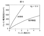
次に、本実施例の効果について特性図13を用いて説明する。図は、耐圧600V以上確保できる条件での電流密度を示しており、従来のpボディ領域が広い(4um)の場合と、本実施例の0.2 umの場合をしたものを示している。従来に比べて本実施例の電流密度は2倍以上になっている。ただし、すでに述べたとおり、n+のシート抵抗やチャネル移動度の向上によりさらに大きな電流を流せるようになる見込みである。 Next, the effect of the present embodiment will be described with reference to the characteristic diagram 13. The figure shows the current density under the condition that a withstand voltage of 600 V or more can be secured, and shows the case where the conventional p body region is wide (4 um) and the case of 0.2 um in this embodiment. The current density of this embodiment is more than twice that of the prior art. However, as already mentioned, it is expected that larger currents can be flowed by improving n + sheet resistance and channel mobility.
本発明の実施例2の断面構造図を図14に示す。本実施例の実施例1との違いはトレンチ側壁近傍にチャネルドープしpボディ領域3の濃度よりもチャネルの濃度を下げている点にある。pボディ領域3よりも濃度の低いチャネル層10を形成することにより、実施例1よりも閾値電圧を下げることができ、電流密度を上げることができる。
FIG. 14 shows a cross-sectional structure diagram of Example 2 of the present invention. The difference between the present embodiment and the first embodiment is that the channel concentration is made lower than the concentration of the
本実施例の作製プロセスは、基本的には実施例1と同様であるが、トレンチを形成した後に斜めイオン注入によりチャネル層を形成する点のみ異なる。斜めイオン注入の条件は15 keV、ドーズは5×1011cm-2である。他の設計値は実施例1と同様である。チャネルドープによりトレンチ側壁から約50 nmの幅で5×1016 cm-3程度のチャネル層を形成した。特性としては、実施例1よりも耐圧600Vを確保した上で、閾値電圧が約0.5V低減し、電流密度が約2割向上した。ただし、チャネルドープをやりすぎると耐圧が低下するだけでなく、チャネル移動度が低下したり、ゲート絶縁膜の信頼性を劣化させる要因にもなるので注意が必要である。 The manufacturing process of this example is basically the same as that of Example 1, except that a channel layer is formed by oblique ion implantation after forming a trench. The conditions for oblique ion implantation are 15 keV and the dose is 5 × 10 11 cm −2. Other design values are the same as those in the first embodiment. A channel layer of about 5 × 10 16 cm −3 with a width of about 50 nm was formed from the sidewall of the trench by channel doping. As characteristics, after securing a withstand voltage of 600 V as compared with Example 1, the threshold voltage was reduced by about 0.5 V, and the current density was improved by about 20%. However, it should be noted that excessive channel doping not only lowers the breakdown voltage but also causes a decrease in channel mobility and a deterioration in the reliability of the gate insulating film.
次に、本発明の実施例3を図15に示すデバイス平面構造図を用いて説明する。本実施例の実施例1との違いは、pボディ領域の幅が広い領域3’と狭い領域3の位置関係にある。実施例1ではpボディ領域の幅が広い領域3’と狭い領域3が直行するようなレイアウトになっているが、本実施例ではpボディ領域の幅が広い領域3’を格子状にして、その間をpボディ領域の幅が狭い領域3がつなぐレイアウトとなっている。
Next,
本実施例の作製方法および動作については実施例1と同様である。ただし、どちらが最適かは状況により異なる。例えばpボディ領域の幅が広い領域3’の幅がpボディ領域の幅が狭い領域3の奥行きよりも広い場合は本実施例のほうが面積的に有利となる。実施例1ではpボディ領域の幅が広い領域3’の幅が4 um、pボディ領域の幅が狭い領域3の奥行きが2 umであるため、本実施例のほうが実施例1に比べ面積的にpボディの幅が狭い領域3が3割程度増え、チャネル抵抗が小さくなる。一方、n+のシート抵抗が低減され、pボディ領域の幅が狭い領域3の奥行きが長くてもソース抵抗が低く保たれる状況においては実施例1のほうが有利となる。
The manufacturing method and operation of this example are the same as those of Example 1. However, which is optimal depends on the situation. For example, when the width of the
実施例1と実施例3を組み合わせたものも容易に想像できるが、状況によってはこの組み合わせが最適の場合もありえる。また、これらの実施例はすべて炭化珪素基板を例に説明したが、シリコンや窒化ガリウムなどどのような半導体にでも適用可能である。 A combination of Example 1 and Example 3 can be easily imagined, but this combination may be optimal depending on the situation. Further, all of these embodiments have been described by taking the silicon carbide substrate as an example, but the present invention can be applied to any semiconductor such as silicon or gallium nitride.
チャネル移動度が大きく、耐圧を落とすことなく閾値電圧が下げられるUMOSFETをパワー半導体素子に用いることができる。 A UMOSFET having a large channel mobility and capable of lowering the threshold voltage without lowering the withstand voltage can be used for a power semiconductor element.
1 ドレイン領域
2 ドリフト領域
3 ボディ領域
4 ソース領域
5 ゲート絶縁膜
6 ドレイン電極
7 ゲート電極
8 pボディ電位固定用p+層
9 ソース電極
1 Drain region
2 Drift region
3 Body area
4 Source area
5 Gate insulation film
6 Drain electrode
7 Gate electrode
8 p p + layer for body potential fixation
9 Source electrode
Claims (20)
前記半導体基板の裏面に接続されている第1の主電極と、
前記半導体基板上に形成されている前記半導体基板よりも低い濃度の第1導電型のエピタキシャル層と、
前記エピタキシャル層中に形成されている第2導電型のボディ領域と、
前記ボディ領域上に形成されている前記エピタキシャル層よりも高い濃度の第1導電型のソース層と、
前記ボディ領域と接続し前記半導体基板表面に形成されている第2導電型のボディ接続層と、
前記ソース層および前記ボディ接続層に接続されている第2の主電極と、
前記ボディ領域と前記ソース層を貫くように形成されているトレンチと、
前記トレンチの側壁および底部に形成されているゲート絶縁膜と、
前記トレンチ内部に形成されている第3の主電極と、を備え、
前記半導体基板および前記エピタキシャル層の材質が炭化珪素であり、
前記トレンチとトレンチで挟まれている前記ボディ領域の幅が少なくとも2種類以上あり、
前記ボディ領域幅が狭い領域のほうが前記ボディ領域幅が広い領域に比べボディ領域の濃度が低く、かつ前記ボディ領域幅が広い領域のほうが前記ボディ接続層に比べ濃度が低く、
前記ボディ領域の幅が狭い領域の幅が、両側の第3の主電極から前記ゲート絶縁膜を介して延びる最大空乏層幅の和よりも狭いことを特徴とする半導体装置。 A semiconductor substrate of a first conductivity type,
A first main electrode connected to the back surface of the semiconductor substrate,
An epitaxial layer of a first conductivity type lower concentration than the semiconductor substrate which is formed on the semiconductor substrate,
A body region of a second conductivity type formed in said epitaxial layer,
A source layer of a first conductivity type having a higher concentration than the epitaxial layer formed on the body region;
A second conductivity type body connection layer formed in connection with the body region and the semiconductor substrate surface,
A second main electrode connected to the source layer and the body connecting layer,
A trench formed to penetrate the body region and the source layer;
A gate insulating film formed on the sidewall and bottom of the trench;
A third main electrode formed inside the trench,
The material of the semiconductor substrate and the epitaxial layer is silicon carbide,
The width of the body region sandwiched by the trenches and trenches are at least two or more,
It said body region width is lower that the concentration of the body region than within the body region wider region towards the narrow region and the low concentration compared to the body connecting layer towards the body region wider region,
A semiconductor device, wherein a width of the narrow body region is narrower than a sum of maximum depletion layer widths extending from third main electrodes on both sides through the gate insulating film.
濃度よりも濃度が低いことを特徴とする請求項1記載の半導体装置。 2. The semiconductor device according to claim 1, wherein a concentration of a region near the gate insulating film in the body region is lower than a concentration of a region away from the gate insulating film.
(b)前記エピタキシャル層中に第2導電型のボディ領域を形成する工程、
(c)前記ボディ領域上に前記エピタキシャル層よりも高い濃度の第1導電型のソース層を形成する工程、
(d)前記ボディ領域と接続するように前記半導体基板表面に第2導電型のボディ接続層を形成する工程、
(e)前記ボディ領域と前記ソース層を貫くようにトレンチを形成する工程、
(f)前記トレンチの側壁および底部にゲート絶縁膜を形成する工程、を含み、
前記半導体基板および前記エピタキシャル層の材質が炭化珪素であり、
前記トレンチとトレンチで挟まれた前記ボディ領域の幅を少なくとも2種類以上異なる幅に形成し、
前記ボディ領域幅が狭い領域のほうが前記ボディ領域幅が広い領域に比べボディ領域の濃度が低く、かつ前記ボディ領域幅が広い領域のほうが前記ボディ接続層に比べ濃度が低くなるようにドーパントをイオン注入し、
前記ボディ領域の幅が狭い領域の幅が、両側の第3の主電極から前記ゲート絶縁膜を介して延びる最大空乏層幅の和よりも狭いことを特徴とする半導体装置の製造方法。 (a) an epitaxial layer of the first conductivity type is formed, the step of preparing a first conductivity type semiconductor substrate a higher concentration than the epitaxial layer,
(b) forming a second conductivity type body region in the epitaxial layer;
(c) forming a first conductivity type source layer of the higher concentration than the epitaxial layer on the body region,
(d) forming a body connecting layer of the second conductivity type in the semiconductor substrate surface so as to connect with said body region,
(e) forming a trench so as to penetrate the body region and the source layer;
(f) forming a gate insulating film on the sidewall and bottom of the trench,
The material of the semiconductor substrate and the epitaxial layer is silicon carbide,
Forming at least two different widths of the body region sandwiched between the trench and the trench,
It said body region width is lower that the concentration of the body region than within the region body region wider towards the narrow region, and the dopant so that concentration than that in the body connecting layer towards the said body region wider region becomes lower ion Inject,
A method of manufacturing a semiconductor device, wherein a width of the narrow body region is narrower than a sum of maximum depletion layer widths extending from third main electrodes on both sides through the gate insulating film.
Priority Applications (2)
| Application Number | Priority Date | Filing Date | Title |
|---|---|---|---|
| JP2009169693A JP5586887B2 (en) | 2009-07-21 | 2009-07-21 | Semiconductor device and manufacturing method thereof |
| US12/834,764 US8564060B2 (en) | 2009-07-21 | 2010-07-12 | Semiconductor device with large blocking voltage and manufacturing method thereof |
Applications Claiming Priority (1)
| Application Number | Priority Date | Filing Date | Title |
|---|---|---|---|
| JP2009169693A JP5586887B2 (en) | 2009-07-21 | 2009-07-21 | Semiconductor device and manufacturing method thereof |
Publications (2)
| Publication Number | Publication Date |
|---|---|
| JP2011023675A JP2011023675A (en) | 2011-02-03 |
| JP5586887B2 true JP5586887B2 (en) | 2014-09-10 |
Family
ID=43496502
Family Applications (1)
| Application Number | Title | Priority Date | Filing Date |
|---|---|---|---|
| JP2009169693A Expired - Fee Related JP5586887B2 (en) | 2009-07-21 | 2009-07-21 | Semiconductor device and manufacturing method thereof |
Country Status (2)
| Country | Link |
|---|---|
| US (1) | US8564060B2 (en) |
| JP (1) | JP5586887B2 (en) |
Families Citing this family (24)
| Publication number | Priority date | Publication date | Assignee | Title |
|---|---|---|---|---|
| US9142662B2 (en) * | 2011-05-06 | 2015-09-22 | Cree, Inc. | Field effect transistor devices with low source resistance |
| US9029945B2 (en) | 2011-05-06 | 2015-05-12 | Cree, Inc. | Field effect transistor devices with low source resistance |
| WO2013036370A1 (en) | 2011-09-11 | 2013-03-14 | Cree, Inc. | High current density power module comprising transistors with improved layout |
| US9373617B2 (en) | 2011-09-11 | 2016-06-21 | Cree, Inc. | High current, low switching loss SiC power module |
| US9640617B2 (en) | 2011-09-11 | 2017-05-02 | Cree, Inc. | High performance power module |
| JP2013232533A (en) | 2012-04-27 | 2013-11-14 | Rohm Co Ltd | Semiconductor device and semiconductor device manufacturing method |
| JP6064366B2 (en) * | 2012-05-18 | 2017-01-25 | 住友電気工業株式会社 | Semiconductor device |
| JP5751213B2 (en) * | 2012-06-14 | 2015-07-22 | 株式会社デンソー | Silicon carbide semiconductor device and manufacturing method thereof |
| JP5880311B2 (en) | 2012-06-26 | 2016-03-09 | 住友電気工業株式会社 | Silicon carbide semiconductor device |
| US9941403B2 (en) * | 2012-09-26 | 2018-04-10 | Infineon Technologies Ag | Semiconductor device and method for manufacturing a semiconductor device |
| JP5888214B2 (en) * | 2012-11-30 | 2016-03-16 | 富士電機株式会社 | Nitride-based compound semiconductor device and manufacturing method thereof |
| CN104347710B (en) * | 2013-08-09 | 2017-03-15 | 无锡华润华晶微电子有限公司 | A kind of bar shaped structure cell of VDMOS device and preparation method thereof |
| US10211304B2 (en) | 2013-12-04 | 2019-02-19 | General Electric Company | Semiconductor device having gate trench in JFET region |
| JP6283122B2 (en) * | 2014-11-26 | 2018-02-21 | 株式会社日立製作所 | Semiconductor switching element and method for manufacturing silicon carbide semiconductor device |
| DE102015108091A1 (en) * | 2015-05-21 | 2016-11-24 | Infineon Technologies Dresden Gmbh | Transistor arrangement with power transistors and voltage-limiting components |
| WO2017133904A1 (en) | 2016-02-02 | 2017-08-10 | Abb Schweiz Ag | Power semiconductor device |
| EP3264470A1 (en) * | 2016-06-29 | 2018-01-03 | ABB Schweiz AG | Short channel trench power mosfet |
| JP6801323B2 (en) | 2016-09-14 | 2020-12-16 | 富士電機株式会社 | Semiconductor devices and methods for manufacturing semiconductor devices |
| JP6848316B2 (en) | 2016-10-05 | 2021-03-24 | 富士電機株式会社 | Semiconductor devices and methods for manufacturing semiconductor devices |
| JP6784921B2 (en) | 2017-02-17 | 2020-11-18 | 株式会社デンソー | Switching element and its manufacturing method |
| GB2572442A (en) * | 2018-03-29 | 2019-10-02 | Cambridge Entpr Ltd | Power semiconductor device with a double gate structure |
| JP2020126932A (en) * | 2019-02-05 | 2020-08-20 | トヨタ自動車株式会社 | Trench gate type semiconductor device |
| JP7443924B2 (en) | 2020-05-14 | 2024-03-06 | 富士電機株式会社 | semiconductor equipment |
| JP7532921B2 (en) | 2020-06-09 | 2024-08-14 | 富士電機株式会社 | Semiconductor Device |
Family Cites Families (10)
| Publication number | Priority date | Publication date | Assignee | Title |
|---|---|---|---|---|
| JPH05110091A (en) | 1991-10-17 | 1993-04-30 | Seiko Epson Corp | Semiconductor device |
| JP3319215B2 (en) | 1995-03-31 | 2002-08-26 | 株式会社豊田中央研究所 | Insulated gate semiconductor device and method of manufacturing the same |
| JPH11214685A (en) * | 1998-01-27 | 1999-08-06 | Matsushita Electric Works Ltd | Insulated gate semiconductor device |
| JP2000058823A (en) * | 1998-08-13 | 2000-02-25 | Toshiba Corp | Semiconductor device and method of manufacturing the same |
| JP4604444B2 (en) * | 2002-12-24 | 2011-01-05 | トヨタ自動車株式会社 | Embedded gate type semiconductor device |
| JP2007043123A (en) * | 2005-07-01 | 2007-02-15 | Toshiba Corp | Semiconductor device |
| JP4928753B2 (en) * | 2005-07-14 | 2012-05-09 | 株式会社東芝 | Trench gate type semiconductor device |
| JP4564514B2 (en) * | 2007-05-18 | 2010-10-20 | 株式会社東芝 | Semiconductor device |
| JP4798119B2 (en) * | 2007-11-06 | 2011-10-19 | 株式会社デンソー | Silicon carbide semiconductor device and manufacturing method thereof |
| JP4640436B2 (en) * | 2008-04-14 | 2011-03-02 | 株式会社デンソー | Method for manufacturing silicon carbide semiconductor device |
-
2009
- 2009-07-21 JP JP2009169693A patent/JP5586887B2/en not_active Expired - Fee Related
-
2010
- 2010-07-12 US US12/834,764 patent/US8564060B2/en not_active Expired - Fee Related
Also Published As
| Publication number | Publication date |
|---|---|
| US8564060B2 (en) | 2013-10-22 |
| US20110018004A1 (en) | 2011-01-27 |
| JP2011023675A (en) | 2011-02-03 |
Similar Documents
| Publication | Publication Date | Title |
|---|---|---|
| JP5586887B2 (en) | Semiconductor device and manufacturing method thereof | |
| US12300724B2 (en) | Method of manufacturing silicon carbide semiconductor devices | |
| CN100555663C (en) | Silicon carbide device and method for manufacturing same | |
| JP4744958B2 (en) | Semiconductor device and manufacturing method thereof | |
| US7723783B2 (en) | Semiconductor device | |
| US7642597B2 (en) | Power semiconductor device | |
| US10276709B2 (en) | Semiconductor device and method of manufacturing semiconductor device | |
| US8519476B2 (en) | Method of forming a self-aligned charge balanced power DMOS | |
| CN102959711B (en) | Semiconductor device and method for manufacturing same | |
| CN108735817A (en) | SiC semiconductor device with the offset in channel bottom | |
| CN105103297A (en) | Semiconductor device with reduced electric field at gate oxide layer | |
| CN111384179A (en) | Silicon carbide semiconductor device and method for manufacturing the same | |
| US11355630B2 (en) | Trench bottom shielding methods and approaches for trenched semiconductor device structures | |
| JP4678902B2 (en) | Silicon carbide UMOS semiconductor device and method of manufacturing the same | |
| JP7017733B2 (en) | Semiconductor devices and methods for manufacturing semiconductor devices | |
| TW202234712A (en) | Sic mosfet with reduced channel length and high vth | |
| JP2023076986A (en) | Semiconductor device and its manufacturing method | |
| US20080038890A1 (en) | Method for improved trench protection in vertical umosfet devices | |
| JP6651801B2 (en) | Semiconductor device and method of manufacturing semiconductor device | |
| JP7755242B2 (en) | Silicon carbide semiconductor device and method for manufacturing silicon carbide semiconductor device | |
| JP2010027833A (en) | Silicon carbide semiconductor device and its manufacturing method | |
| WO2015111177A1 (en) | Semiconductor device, power module, power conversion device, and railway vehicle | |
| JP5059989B1 (en) | Semiconductor device and manufacturing method thereof | |
| JP2021028962A (en) | Silicon carbide semiconductor device | |
| JP3541832B2 (en) | Field effect transistor and method of manufacturing the same |
Legal Events
| Date | Code | Title | Description |
|---|---|---|---|
| A621 | Written request for application examination |
Free format text: JAPANESE INTERMEDIATE CODE: A621 Effective date: 20120224 |
|
| A977 | Report on retrieval |
Free format text: JAPANESE INTERMEDIATE CODE: A971007 Effective date: 20131007 |
|
| A131 | Notification of reasons for refusal |
Free format text: JAPANESE INTERMEDIATE CODE: A131 Effective date: 20131015 |
|
| A521 | Request for written amendment filed |
Free format text: JAPANESE INTERMEDIATE CODE: A523 Effective date: 20131209 |
|
| A131 | Notification of reasons for refusal |
Free format text: JAPANESE INTERMEDIATE CODE: A131 Effective date: 20140128 |
|
| A521 | Request for written amendment filed |
Free format text: JAPANESE INTERMEDIATE CODE: A523 Effective date: 20140331 |
|
| TRDD | Decision of grant or rejection written | ||
| A01 | Written decision to grant a patent or to grant a registration (utility model) |
Free format text: JAPANESE INTERMEDIATE CODE: A01 Effective date: 20140624 |
|
| A61 | First payment of annual fees (during grant procedure) |
Free format text: JAPANESE INTERMEDIATE CODE: A61 Effective date: 20140723 |
|
| R151 | Written notification of patent or utility model registration |
Ref document number: 5586887 Country of ref document: JP Free format text: JAPANESE INTERMEDIATE CODE: R151 |
|
| LAPS | Cancellation because of no payment of annual fees |