JP4082400B2 - Electro-optical device manufacturing method, electro-optical device, and electronic apparatus - Google Patents
Electro-optical device manufacturing method, electro-optical device, and electronic apparatus Download PDFInfo
- Publication number
- JP4082400B2 JP4082400B2 JP2004288665A JP2004288665A JP4082400B2 JP 4082400 B2 JP4082400 B2 JP 4082400B2 JP 2004288665 A JP2004288665 A JP 2004288665A JP 2004288665 A JP2004288665 A JP 2004288665A JP 4082400 B2 JP4082400 B2 JP 4082400B2
- Authority
- JP
- Japan
- Prior art keywords
- substrate
- small
- electro
- optical device
- manufacturing
- Prior art date
- Legal status (The legal status is an assumption and is not a legal conclusion. Google has not performed a legal analysis and makes no representation as to the accuracy of the status listed.)
- Expired - Fee Related
Links
- 238000004519 manufacturing process Methods 0.000 title claims description 73
- 239000000758 substrate Substances 0.000 claims description 906
- 238000000034 method Methods 0.000 claims description 134
- 238000007789 sealing Methods 0.000 claims description 128
- 239000002346 layers by function Substances 0.000 claims description 57
- 239000000463 material Substances 0.000 claims description 55
- 230000001681 protective effect Effects 0.000 claims description 55
- 238000005498 polishing Methods 0.000 claims description 49
- 239000010410 layer Substances 0.000 claims description 47
- 239000007788 liquid Substances 0.000 claims description 35
- 230000015572 biosynthetic process Effects 0.000 claims description 33
- 239000011347 resin Substances 0.000 claims description 32
- 229920005989 resin Polymers 0.000 claims description 32
- 239000000853 adhesive Substances 0.000 claims description 26
- 230000001070 adhesive effect Effects 0.000 claims description 26
- 238000005192 partition Methods 0.000 claims description 25
- 239000012530 fluid Substances 0.000 claims description 21
- 239000000203 mixture Substances 0.000 claims description 20
- 238000005520 cutting process Methods 0.000 claims description 16
- 239000011342 resin composition Substances 0.000 claims description 12
- 238000000206 photolithography Methods 0.000 claims description 11
- 239000005871 repellent Substances 0.000 claims description 10
- 230000002940 repellent Effects 0.000 claims description 9
- 238000003698 laser cutting Methods 0.000 claims description 8
- 238000007639 printing Methods 0.000 claims description 8
- 238000012546 transfer Methods 0.000 claims description 8
- 239000011159 matrix material Substances 0.000 claims description 6
- 239000012790 adhesive layer Substances 0.000 claims description 5
- 230000003287 optical effect Effects 0.000 claims 2
- 239000011248 coating agent Substances 0.000 claims 1
- 238000000576 coating method Methods 0.000 claims 1
- 230000005611 electricity Effects 0.000 claims 1
- 239000010408 film Substances 0.000 description 82
- 239000001993 wax Substances 0.000 description 38
- 239000011521 glass Substances 0.000 description 16
- 238000005401 electroluminescence Methods 0.000 description 13
- 238000002347 injection Methods 0.000 description 9
- 239000007924 injection Substances 0.000 description 9
- 230000001276 controlling effect Effects 0.000 description 8
- 238000010586 diagram Methods 0.000 description 7
- 239000003822 epoxy resin Substances 0.000 description 7
- 238000002844 melting Methods 0.000 description 7
- 230000008018 melting Effects 0.000 description 7
- 229920000647 polyepoxide Polymers 0.000 description 7
- 239000003522 acrylic cement Substances 0.000 description 6
- 229910052782 aluminium Inorganic materials 0.000 description 6
- 239000004973 liquid crystal related substance Substances 0.000 description 6
- 239000002245 particle Substances 0.000 description 6
- 239000004065 semiconductor Substances 0.000 description 6
- 238000003486 chemical etching Methods 0.000 description 5
- 230000000694 effects Effects 0.000 description 5
- 238000005224 laser annealing Methods 0.000 description 5
- 239000006061 abrasive grain Substances 0.000 description 4
- XAGFODPZIPBFFR-UHFFFAOYSA-N aluminium Chemical compound [Al] XAGFODPZIPBFFR-UHFFFAOYSA-N 0.000 description 4
- 239000003990 capacitor Substances 0.000 description 4
- 230000007423 decrease Effects 0.000 description 4
- 238000010438 heat treatment Methods 0.000 description 4
- 239000011229 interlayer Substances 0.000 description 4
- 230000002093 peripheral effect Effects 0.000 description 4
- 238000007517 polishing process Methods 0.000 description 4
- 239000000725 suspension Substances 0.000 description 4
- OYPRJOBELJOOCE-UHFFFAOYSA-N Calcium Chemical compound [Ca] OYPRJOBELJOOCE-UHFFFAOYSA-N 0.000 description 3
- 229920000265 Polyparaphenylene Polymers 0.000 description 3
- 239000004820 Pressure-sensitive adhesive Substances 0.000 description 3
- 241000135309 Processus Species 0.000 description 3
- 239000011575 calcium Substances 0.000 description 3
- 229910052791 calcium Inorganic materials 0.000 description 3
- 239000012141 concentrate Substances 0.000 description 3
- 238000005516 engineering process Methods 0.000 description 3
- 238000000227 grinding Methods 0.000 description 3
- 230000001678 irradiating effect Effects 0.000 description 3
- 239000011368 organic material Substances 0.000 description 3
- 229910021420 polycrystalline silicon Inorganic materials 0.000 description 3
- 229920005591 polysilicon Polymers 0.000 description 3
- 239000003566 sealing material Substances 0.000 description 3
- UJOBWOGCFQCDNV-UHFFFAOYSA-N 9H-carbazole Chemical compound C1=CC=C2C3=CC=CC=C3NC2=C1 UJOBWOGCFQCDNV-UHFFFAOYSA-N 0.000 description 2
- 239000004925 Acrylic resin Substances 0.000 description 2
- 229920000178 Acrylic resin Polymers 0.000 description 2
- 229920001609 Poly(3,4-ethylenedioxythiophene) Polymers 0.000 description 2
- 238000004140 cleaning Methods 0.000 description 2
- 239000003086 colorant Substances 0.000 description 2
- 230000006866 deterioration Effects 0.000 description 2
- 239000006185 dispersion Substances 0.000 description 2
- 238000001035 drying Methods 0.000 description 2
- 230000005281 excited state Effects 0.000 description 2
- 239000004744 fabric Substances 0.000 description 2
- 239000000155 melt Substances 0.000 description 2
- 238000009832 plasma treatment Methods 0.000 description 2
- -1 polyphenylene Polymers 0.000 description 2
- 239000000243 solution Substances 0.000 description 2
- 238000002834 transmittance Methods 0.000 description 2
- OAICVXFJPJFONN-UHFFFAOYSA-N Phosphorus Chemical compound [P] OAICVXFJPJFONN-UHFFFAOYSA-N 0.000 description 1
- 229910004298 SiO 2 Inorganic materials 0.000 description 1
- VYPSYNLAJGMNEJ-UHFFFAOYSA-N Silicium dioxide Chemical compound O=[Si]=O VYPSYNLAJGMNEJ-UHFFFAOYSA-N 0.000 description 1
- 229910010413 TiO 2 Inorganic materials 0.000 description 1
- 239000002313 adhesive film Substances 0.000 description 1
- 229910021417 amorphous silicon Inorganic materials 0.000 description 1
- 125000002490 anilino group Chemical class [H]N(*)C1=C([H])C([H])=C([H])C([H])=C1[H] 0.000 description 1
- QVGXLLKOCUKJST-UHFFFAOYSA-N atomic oxygen Chemical compound [O] QVGXLLKOCUKJST-UHFFFAOYSA-N 0.000 description 1
- 239000000919 ceramic Substances 0.000 description 1
- 229920001940 conductive polymer Polymers 0.000 description 1
- 238000007796 conventional method Methods 0.000 description 1
- 238000007599 discharging Methods 0.000 description 1
- 125000005678 ethenylene group Chemical group [H]C([*:1])=C([H])[*:2] 0.000 description 1
- 125000003983 fluorenyl group Chemical class C1(=CC=CC=2C3=CC=CC=C3CC12)* 0.000 description 1
- 150000002222 fluorine compounds Chemical class 0.000 description 1
- 239000003292 glue Substances 0.000 description 1
- 230000005283 ground state Effects 0.000 description 1
- RBTKNAXYKSUFRK-UHFFFAOYSA-N heliogen blue Chemical compound [Cu].[N-]1C2=C(C=CC=C3)C3=C1N=C([N-]1)C3=CC=CC=C3C1=NC([N-]1)=C(C=CC=C3)C3=C1N=C([N-]1)C3=CC=CC=C3C1=N2 RBTKNAXYKSUFRK-UHFFFAOYSA-N 0.000 description 1
- 229910010272 inorganic material Inorganic materials 0.000 description 1
- 239000011147 inorganic material Substances 0.000 description 1
- 230000009545 invasion Effects 0.000 description 1
- 238000005468 ion implantation Methods 0.000 description 1
- 238000010030 laminating Methods 0.000 description 1
- 238000012986 modification Methods 0.000 description 1
- 230000004048 modification Effects 0.000 description 1
- 229910052750 molybdenum Inorganic materials 0.000 description 1
- 230000003647 oxidation Effects 0.000 description 1
- 238000007254 oxidation reaction Methods 0.000 description 1
- 239000001301 oxygen Substances 0.000 description 1
- 229910052760 oxygen Inorganic materials 0.000 description 1
- 230000035515 penetration Effects 0.000 description 1
- 229910052698 phosphorus Inorganic materials 0.000 description 1
- 239000011574 phosphorus Substances 0.000 description 1
- 229920000548 poly(silane) polymer Polymers 0.000 description 1
- 229920000172 poly(styrenesulfonic acid) Polymers 0.000 description 1
- 229920000767 polyaniline Polymers 0.000 description 1
- 229920001721 polyimide Polymers 0.000 description 1
- 239000009719 polyimide resin Substances 0.000 description 1
- 229920000128 polypyrrole Polymers 0.000 description 1
- 229940005642 polystyrene sulfonic acid Drugs 0.000 description 1
- 229920000123 polythiophene Polymers 0.000 description 1
- 238000012545 processing Methods 0.000 description 1
- 230000001105 regulatory effect Effects 0.000 description 1
- 229910052814 silicon oxide Inorganic materials 0.000 description 1
- 229910052709 silver Inorganic materials 0.000 description 1
- 238000007711 solidification Methods 0.000 description 1
- 230000008023 solidification Effects 0.000 description 1
- 239000002904 solvent Substances 0.000 description 1
- 229910052715 tantalum Inorganic materials 0.000 description 1
- 239000010409 thin film Substances 0.000 description 1
- 229910052719 titanium Inorganic materials 0.000 description 1
- 229910052721 tungsten Inorganic materials 0.000 description 1
- 238000007740 vapor deposition Methods 0.000 description 1
- 229920002554 vinyl polymer Polymers 0.000 description 1
- XLYOFNOQVPJJNP-UHFFFAOYSA-N water Substances O XLYOFNOQVPJJNP-UHFFFAOYSA-N 0.000 description 1
Images


Classifications
-
- H—ELECTRICITY
- H10—SEMICONDUCTOR DEVICES; ELECTRIC SOLID-STATE DEVICES NOT OTHERWISE PROVIDED FOR
- H10K—ORGANIC ELECTRIC SOLID-STATE DEVICES
- H10K59/00—Integrated devices, or assemblies of multiple devices, comprising at least one organic light-emitting element covered by group H10K50/00
- H10K59/10—OLED displays
- H10K59/18—Tiled displays
-
- A—HUMAN NECESSITIES
- A01—AGRICULTURE; FORESTRY; ANIMAL HUSBANDRY; HUNTING; TRAPPING; FISHING
- A01K—ANIMAL HUSBANDRY; AVICULTURE; APICULTURE; PISCICULTURE; FISHING; REARING OR BREEDING ANIMALS, NOT OTHERWISE PROVIDED FOR; NEW BREEDS OF ANIMALS
- A01K61/00—Culture of aquatic animals
- A01K61/60—Floating cultivation devices, e.g. rafts or floating fish-farms
- A01K61/65—Connecting or mooring devices therefor
-
- H—ELECTRICITY
- H10—SEMICONDUCTOR DEVICES; ELECTRIC SOLID-STATE DEVICES NOT OTHERWISE PROVIDED FOR
- H10K—ORGANIC ELECTRIC SOLID-STATE DEVICES
- H10K71/00—Manufacture or treatment specially adapted for the organic devices covered by this subclass
-
- H—ELECTRICITY
- H10—SEMICONDUCTOR DEVICES; ELECTRIC SOLID-STATE DEVICES NOT OTHERWISE PROVIDED FOR
- H10K—ORGANIC ELECTRIC SOLID-STATE DEVICES
- H10K2102/00—Constructional details relating to the organic devices covered by this subclass
- H10K2102/301—Details of OLEDs
- H10K2102/302—Details of OLEDs of OLED structures
- H10K2102/3023—Direction of light emission
- H10K2102/3031—Two-side emission, e.g. transparent OLEDs [TOLED]
-
- H—ELECTRICITY
- H10—SEMICONDUCTOR DEVICES; ELECTRIC SOLID-STATE DEVICES NOT OTHERWISE PROVIDED FOR
- H10K—ORGANIC ELECTRIC SOLID-STATE DEVICES
- H10K50/00—Organic light-emitting devices
- H10K50/80—Constructional details
- H10K50/84—Passivation; Containers; Encapsulations
- H10K50/842—Containers
- H10K50/8426—Peripheral sealing arrangements, e.g. adhesives, sealants
-
- H—ELECTRICITY
- H10—SEMICONDUCTOR DEVICES; ELECTRIC SOLID-STATE DEVICES NOT OTHERWISE PROVIDED FOR
- H10K—ORGANIC ELECTRIC SOLID-STATE DEVICES
- H10K59/00—Integrated devices, or assemblies of multiple devices, comprising at least one organic light-emitting element covered by group H10K50/00
- H10K59/10—OLED displays
- H10K59/12—Active-matrix OLED [AMOLED] displays
-
- H—ELECTRICITY
- H10—SEMICONDUCTOR DEVICES; ELECTRIC SOLID-STATE DEVICES NOT OTHERWISE PROVIDED FOR
- H10K—ORGANIC ELECTRIC SOLID-STATE DEVICES
- H10K59/00—Integrated devices, or assemblies of multiple devices, comprising at least one organic light-emitting element covered by group H10K50/00
- H10K59/80—Constructional details
- H10K59/87—Passivation; Containers; Encapsulations
- H10K59/871—Self-supporting sealing arrangements
- H10K59/8722—Peripheral sealing arrangements, e.g. adhesives, sealants
-
- Y—GENERAL TAGGING OF NEW TECHNOLOGICAL DEVELOPMENTS; GENERAL TAGGING OF CROSS-SECTIONAL TECHNOLOGIES SPANNING OVER SEVERAL SECTIONS OF THE IPC; TECHNICAL SUBJECTS COVERED BY FORMER USPC CROSS-REFERENCE ART COLLECTIONS [XRACs] AND DIGESTS
- Y02—TECHNOLOGIES OR APPLICATIONS FOR MITIGATION OR ADAPTATION AGAINST CLIMATE CHANGE
- Y02P—CLIMATE CHANGE MITIGATION TECHNOLOGIES IN THE PRODUCTION OR PROCESSING OF GOODS
- Y02P60/00—Technologies relating to agriculture, livestock or agroalimentary industries
- Y02P60/60—Fishing; Aquaculture; Aquafarming
Landscapes
- Life Sciences & Earth Sciences (AREA)
- Engineering & Computer Science (AREA)
- Manufacturing & Machinery (AREA)
- Environmental Sciences (AREA)
- Marine Sciences & Fisheries (AREA)
- Zoology (AREA)
- Animal Husbandry (AREA)
- Biodiversity & Conservation Biology (AREA)
- Electroluminescent Light Sources (AREA)
- Devices For Indicating Variable Information By Combining Individual Elements (AREA)
Description
本発明は、自発光型素子によって多数の画素が構成された電気光学装置の製造方法と、この方法により製造した電気光学装置、およびそれを用いた電子機器に関するものである。 The present invention relates to a method for manufacturing an electro-optical device in which a large number of pixels are configured by self-luminous elements, an electro-optical device manufactured by this method, and an electronic apparatus using the same.
近年、受光型の液晶表示以外にも薄型、軽量、視野角依存性が無い等の特徴を有する有機エレクトロルミネッセンス(以下、ELと略す)表示が、自発光型電気光学装置として注目されている。このような有機EL表示装置では、液晶同様マトリクス状に配置された複数の画素の各々に画素スイッチング素子および有機EL素子を配置した表示基板を用い、各画素のON・OFFを制御することによって表示を行う。有機EL素子は、有機材料を挟む二つの電極と発光に寄与する有機材料から構成される。二つの電極からは、電子とホールが発光材料中に注入されることによって各画素の発光が生じる。すなわち、電極から注入された電子とホールを有機材料の発光中心で再結合させることによって、有機分子を励起状態にし、この後有機分子が励起状態から基底状態へ戻るときに発光を生じさせる。したがって、発光色の違う種々の材料を用いれば、カラー画像を表示することができる。 In recent years, organic electroluminescence (hereinafter abbreviated as EL) displays having features such as thinness, light weight, and no viewing angle dependency other than light-receiving liquid crystal displays have attracted attention as self-luminous electro-optical devices. In such an organic EL display device, a display substrate in which a pixel switching element and an organic EL element are arranged in each of a plurality of pixels arranged in a matrix like a liquid crystal is used, and display is performed by controlling ON / OFF of each pixel. I do. The organic EL element is composed of two electrodes sandwiching an organic material and an organic material that contributes to light emission. From the two electrodes, light is emitted from each pixel by injecting electrons and holes into the light emitting material. That is, by recombining electrons and holes injected from the electrode at the emission center of the organic material, the organic molecule is brought into an excited state, and then light is emitted when the organic molecule returns from the excited state to the ground state. Therefore, a color image can be displayed by using various materials having different emission colors.
このような有機EL表示装置に対して、液晶表示装置と同様に、30インチを越えるような表示装置が要求されており、その場合には基板も大型化する。このため、画素スイッチング用素子のTFT(薄膜トランジスタ)を製造するためのラインが大型化する。また、基板を大型化することによって、洗浄工程や成膜工程での歩留まりが低下する。さらには、基板に安価なガラス基板を用いることを目的に、TFTを低温ポリシリコンTFTで構成しようとすると、アモルファスシリコンをポシリコンに結晶化するためのレーザアニールが不安定となる。 For such an organic EL display device, a display device exceeding 30 inches is required as in the case of a liquid crystal display device. In this case, the substrate is also enlarged. For this reason, the line for manufacturing TFT (thin film transistor) of the element for pixel switching becomes large. In addition, increasing the size of the substrate reduces the yield in the cleaning process and the film forming process. Furthermore, if an attempt is made to construct a TFT with a low-temperature polysilicon TFT for the purpose of using an inexpensive glass substrate, laser annealing for crystallizing amorphous silicon into polysilicon becomes unstable.
そこで、従来の技術で充分製造可能な大きさの基板を複数枚、平面的に配置して大型の有機EL表示装置を構成することが提案されている。このような大型化技術には、小型基板上に画素スイッチング用素子、および有機EL素子を形成してから複数枚の小型基板を平面的に並べる方法と、小型基板上に画素スイッチング用素子を形成してから複数枚の小型基板を平面的に並べ、しかる後、各小型基板上に有機EL素子を形成する方法とが提案されている。後者の場合、小型基板同士の繋ぎ目が目立たないという利点がある(例えば、特許文献1、2参照)。
しかし、特許文献1、2に記載の技術においては、複数枚の小型基板を平面的に並べた状態で有機EL素子を形成する際、従来どおりの半導体プロセスを利用する必要があり、有機EL素子を広い領域にわたって形成するための特別の技術が採用されていない。このため、有機EL素子を形成する際には、製造装置の大型化を避けることができないという問題がある。
However, in the techniques described in
また、複数枚の小型基板を平面的に並べて大型の有機EL表示装置を構成した場合、小型基板の厚さ方向の位置がばらつく、あるいは、小型基板が面の外方向で傾いた場合には、各画素の発光位置がばらついてしまい表示品位が低下するという問題がある。 In addition, when a large organic EL display device is configured by arranging a plurality of small substrates in a plane, the position of the small substrate in the thickness direction varies, or when the small substrate is inclined in the outer direction of the surface, There is a problem that the light emission position of each pixel varies and the display quality deteriorates.
更には、特許文献1、2に記載の技術のように、複数枚の小型基板を大型基板上に貼り合わせたものでは、その大型基板の厚さ分電気光学装置が厚くなり、また軽量化を図れないという問題点がある。更には、基板を湾曲させた新たな形態の電気光学装置を製造できないという問題点がある。しかし、最初から薄い基板を用いた場合には、製造工程中、基板が割れて歩留まりが低下するという問題点がある。そこで、小型基板に大型基板あるいは封止基板(対向基板)を貼り合わせてパネル状にした後、薄型化することが考えられるが、このような薄型化を化学エッチングで行うと、電気光学装置用基板に形成されている端子もエッチングされて損傷するという問題がある。
Further, in the case where a plurality of small substrates are bonded to a large substrate as in the techniques described in
以上の問題点を解決するために、本発明の課題は、製造装置を大型化することなく、複数枚の小型基板を平面的に並べた状態で自発光素子を効率よく形成可能な自発光型の電気光学装置の製造方法と、この方法で製造した電気光学装置、およびこの電気光学装置を備えた電子機器を提供することにある。 In order to solve the above problems, an object of the present invention is to provide a self-luminous type capable of efficiently forming a self-luminous element in a state where a plurality of small substrates are arranged in a plane without increasing the size of a manufacturing apparatus. An electro-optical device manufacturing method, an electro-optical device manufactured by the method, and an electronic apparatus including the electro-optical device are provided.
また、本発明の課題は、複数枚の小型基板を平面的に並べた場合でも、小型基板の厚さ方向の位置にばらつきが発生せず、かつ、小型基板が面の外方向に傾くことのない電気光学装置の製造方法と、この方法で製造した電気光学装置、およびこの電気光学装置を備えた電子機器を提供することにある。 In addition, the problem of the present invention is that even when a plurality of small substrates are arranged in a plane, there is no variation in the position in the thickness direction of the small substrates, and the small substrates are inclined to the outside of the surface. An electro-optical device manufacturing method, an electro-optical device manufactured by the method, and an electronic apparatus including the electro-optical device are provided.
また、本発明の他の課題は、小型基板をその製造工程の途中で効率よく薄型化することが可能な電気光学装置の製造方法と、この方法で製造した電気光学装置、およびそれを備えた電子機器を提供することにある。 Another object of the present invention is to provide an electro-optical device manufacturing method capable of efficiently thinning a small substrate during the manufacturing process, an electro-optical device manufactured by this method, and the same. To provide electronic equipment.
また、更なる本発明の課題は、小型基板と対向基板を貼り合わせたパネルの端子を損傷することなく薄型化することのできる電気光学装置の製造方法と、この方法で製造した電気光学装置、およびそれを用いた電子機器を提供することにある。 Further, another object of the present invention is to provide a method for manufacturing an electro-optical device that can be thinned without damaging a terminal of a panel in which a small substrate and a counter substrate are bonded together, and an electro-optical device manufactured by this method, And providing an electronic device using the same.
上記課題を解決するために、本発明では、マトリクス状に配置された多数の画素領域の各々に画素スイッチング用素子および自発光素子を備えた基板が複数枚、平面的に配列された電気光学装置の製造方法において、小型基板の一方面に、前記画素スイッチング用素子、前記自発光素子の画素電極、及び液状組成物の塗布領域を規定する隔壁を形成する小型基板形成工程と、前記小型基板形成工程の後、前記小型基板の少なくとも前記一方面側に、前記隔壁の高さよりも薄い粘着剤層と前記液状組成物に対する撥液材層とをフィルム基材の一方面側に形成した保護フィルムを貼着する工程と、前記保護フィルムの側を定盤に向けて前記複数枚の小型基板を配列し、前記定盤上に配列させた前記複数枚の小型基板の前記他方面側に前記大型基板を重ね、この状態で、流体圧を前記大型基板に加えて当該大型基板を前記定盤に向けて押し付けて、前記複数枚の小型基板の前記他方面側と前記大型基板とを貼り合わせる、貼り合わせ工程と、前記貼り合わせ工程を行った後、前記保護フィルムを前記小型基板の前記一方面側から除去することにより、前記液状組成物の塗布領域の周囲に前記撥液材層を前記小型基板側に転写する工程と、前記複数枚の小型基板の前記塗布領域に対してインクジェット法により液状組成物を選択的に塗布して、前記自発光素子の発光機能層を形成する発光機能層形成工程と、を有することを特徴とする。
上記課題を解決するために、本発明では、マトリクス状に配置された多数の画素領域の各々に画素スイッチング用素子および自発光素子を備えた基板が、複数枚、平面的に配列された電気光学装置の製造方法において、前記画素スイッチング用素子、および前記自発光素子の画素電極が基板の一方面側に形成された小型基板を形成する小型基板形成工程と、前記小型基板を複数枚、平面的に配列された状態に当該複数枚の小型基板の他方面側を大型基板と貼り合せる貼り合わせ工程と、この状態において、前記複数枚の小型基板の前記一方面側の所定領域に対してインクジェット法により液状組成物を選択的に塗布して前記自発光素子の発光機能層を形成する発光機能層形成工程とを有することを特徴とする。
In order to solve the above problems, in the present invention, an electro-optical device in which a plurality of substrates each having a pixel switching element and a self-light emitting element are arranged in a plane in each of a large number of pixel regions arranged in a matrix. In the manufacturing method, the small substrate forming step of forming a partition for defining the pixel switching element, the pixel electrode of the self-luminous element, and the application region of the liquid composition on one surface of the small substrate, and forming the small substrate After the step, a protective film in which a pressure-sensitive adhesive layer thinner than the partition wall and a liquid repellent layer for the liquid composition are formed on one side of the film base on at least one side of the small substrate. The step of attaching, the plurality of small substrates are arranged with the protective film side facing the surface plate, and the large substrate on the other surface side of the plurality of small substrates arranged on the surface plate In this state, fluid pressure is applied to the large substrate, the large substrate is pressed toward the surface plate, and the other surface side of the plurality of small substrates is bonded to the large substrate. After performing the step and the bonding step, the protective film is removed from the one surface side of the small substrate, whereby the liquid repellent material layer is placed around the application region of the liquid composition on the small substrate side And a light emitting functional layer forming step of selectively applying a liquid composition to the application regions of the plurality of small substrates by an ink jet method to form a light emitting functional layer of the light emitting element. It is characterized by having.
In order to solve the above-described problems, in the present invention, an electro-optical device in which a plurality of substrates each including a pixel switching element and a self-light emitting element are arranged in a plurality of planes in each of a large number of pixel regions arranged in a matrix. In the manufacturing method of the device, a small substrate forming step of forming a small substrate in which the pixel switching element and the pixel electrode of the self-light-emitting element are formed on one side of the substrate, and a plurality of the small substrates are planarly formed. A bonding step in which the other side of the plurality of small substrates is bonded to the large substrate in a state of being arranged in the same, and in this state, an inkjet method is applied to a predetermined region on the one surface side of the plurality of small substrates And a light emitting functional layer forming step of selectively applying a liquid composition to form a light emitting functional layer of the light emitting element.
本発明では、小型基板の画素スイッチング用素子の形成および自発光素子の画素電極の形成など、レーザアニール、フォトリソグラフィ技術等が必要なプロセスについては、大型基板への貼り合せ工程の前に行う。また、この貼り合わせ工程の後、自発光素子の発光機能層形成に、任意の位置への塗布を容易に行うことのできるインクジェット法を採用する。このため、自発光素子の発光機能層形成を、複数枚の小型基板を平面的に並べた広い領域に実施する際でも、装置の大型化や歩留まりの低下が発生しない。 In the present invention, processes that require laser annealing, photolithography, and the like, such as formation of pixel switching elements on a small substrate and formation of pixel electrodes of self-luminous elements, are performed before the bonding process to a large substrate. In addition, after this bonding step, an ink jet method that can be easily applied to an arbitrary position is adopted for forming the light emitting functional layer of the self light emitting element. For this reason, even when the light emitting functional layer formation of the self-luminous element is performed in a wide region in which a plurality of small substrates are arranged in a plane, the size of the device is not increased and the yield is not reduced.
本発明において、前記貼り合わせ工程では、例えば、前記小型基板と前記大型基板とを接着剤で全面接着する。 In the present invention, in the bonding step, for example, the small substrate and the large substrate are bonded together with an adhesive.
本発明において、前記貼り合わせ工程を行う前に、前記小型基板の複数の基板辺のうち、少なくとも前記電気光学装置において、他の小型基板と隣接する辺をレーザにより切断するレーザ切断工程を行うことが好ましい。このような構成にすれば、小型基板同士を正確に接合できるので、大型基板上における小型基板同士の位置精度が向上する。また、インクジェット法により自発光素子の発光機能層を形成する際、小型基板同士の位置精度が高いので、小型基板上の所定位置に高い精度をもって発光機能層を形成することができる。更には、前記小型基板には、切断のためのレーザの照射位置を示すアライメントマークが形成されていることが好ましい。 In the present invention, before performing the bonding step, a laser cutting step of cutting a side adjacent to another small substrate by laser at least in the electro-optical device among the plurality of substrate sides of the small substrate is performed. Is preferred. With such a configuration, the small substrates can be accurately bonded to each other, so that the positional accuracy between the small substrates on the large substrate is improved. In addition, when forming the light emitting functional layer of the self light emitting element by the ink jet method, the positional accuracy between the small substrates is high, so that the light emitting functional layer can be formed with high accuracy at a predetermined position on the small substrate. Furthermore, it is preferable that an alignment mark indicating a laser irradiation position for cutting is formed on the small substrate.
本発明において、前記小型基板形成工程の後、前記小型基板の少なくとも前記一方面側に保護フィルムを貼着し、次に、前記貼り合わせ工程を行った後、前記保護フィルムを前記小型基板の前記一方面側から除去し、しかる後に、前記発光機能層形成工程を行うことが好ましい。このような構成にすると、貼り合わせ工程の際、小型基板において画素スイッチング素子が形成されている一方面側を異物や損傷から保護することができるので、信頼性を向上させることができる。 In the present invention, after the small substrate forming step, a protective film is attached to at least one side of the small substrate, and then the bonding step is performed, and then the protective film is attached to the small substrate. It is preferable that the light emitting functional layer forming step is performed after removing from one surface side. With such a structure, the one surface side on which the pixel switching element is formed in the small substrate can be protected from foreign matters and damage in the bonding step, so that reliability can be improved.
本発明において、前記貼り合わせ工程では、前記保護フィルムの側を定盤に向けて前記複数枚の小型基板を配列し、この状態で、前記複数枚の小型基板の前記他方面側と前記大型基板とを貼り合わせることが好ましい。このような構成にすると、小型基板の保護フィルムが形成されている一方面側を基準に大型基板の貼り合わせを行うことができる。従って、インクジェット法により自発光素子の発光機能層を形成する際、インクジェットヘッドから小型基板の一方面側との距離がいずれの小型基板においても一定となり、液滴の飛弾距離のばらつきに起因する発光機能層の形成位置や、輝度のばらつきを防止することができる。 In the present invention, in the bonding step, the plurality of small substrates are arranged with the protective film side facing the surface plate, and in this state, the other surface side of the plurality of small substrates and the large substrate. Are preferably pasted together. With such a configuration, the large substrate can be bonded on the basis of the one surface side where the protective film for the small substrate is formed. Therefore, when the light emitting functional layer of the self-light emitting element is formed by the ink jet method, the distance from the ink jet head to the one surface side of the small substrate is constant in any small substrate, and the light emission caused by the variation in the droplet flying distance The formation position of the functional layer and variation in luminance can be prevented.
本発明において、前記貼り合わせ工程では、前記定盤上に配列させた前記複数枚の小型基板の前記他方面側に前記大型基板を重ね、この状態で、流体圧を前記大型基板に加えて当該大型基板を前記定盤に向けて押し付けて、前記複数枚の小型基板の前記他方面側と前記大型基板とを貼り合わせることが好ましい。このような構成にすると、大型基板および小型基板に均一な力が加わるので、いずれの小型基板も大型基板に対して同一条件で貼り合せることができる。そのため、電気光学装置を形成した小型基板の厚さ方向における位置ばらつきを防止し、品位の高い画像を表示することができる。 In the present invention, in the bonding step, the large substrate is overlaid on the other surface side of the plurality of small substrates arranged on the surface plate, and in this state, fluid pressure is applied to the large substrate to It is preferable that the large substrate is pressed toward the surface plate, and the other surface side of the plurality of small substrates is bonded to the large substrate. With such a configuration, since a uniform force is applied to the large substrate and the small substrate, both small substrates can be bonded to the large substrate under the same conditions. Therefore, it is possible to prevent positional variation in the thickness direction of the small substrate on which the electro-optical device is formed, and display a high-quality image.
本発明において、前記貼り合わせ工程では、前記小型基板と前記大型基板との間に、基板間隔を制御する第1の基板間隔制御部材を介在させた状態で、前記小型基板と前記大型基板とを貼り合わせることが好ましい。このような構成にすると、小型基板は第1の基板間隔制御部材によって大型基板と厚さ方向の間隔が規定されるので、小型基板の厚さ方向の位置にばらつきが発生せず、かつ、小型基板が面の外方向に傾くことがない。従って、大型基板側から表示光が出射されるボトムエミッション型表示の場合、観察者からみた各画素の発光位置を揃えることができる。そのため、表示にゆがみのない高品位の有機EL装置を提供できる。また、トップエミッション型およびボトムエミッション型のいずれの表示の場合でも、インクジェット法により自発光素子の発光機能層を形成すれば、インクジェットヘッドから小型基板の一方面側との距離が、いずれの小型基板においても一定であるため、ヘッドからの液滴の飛弾距離のばらつきに起因する発光機能層の形成位置や輝度などのばらつきを防止することができる。従って、本発明は表示品位の向上を図ることができる。 In the present invention, in the bonding step, the small substrate and the large substrate are placed with the first substrate interval control member for controlling the substrate interval interposed between the small substrate and the large substrate. It is preferable to bond them together. With such a configuration, the small substrate has a gap in the thickness direction between the large substrate and the small substrate because the distance between the large substrate and the large substrate is defined by the first substrate interval control member. The substrate does not tilt out of the plane. Therefore, in the case of bottom emission display in which display light is emitted from the large substrate side, the light emission positions of the respective pixels as viewed from the observer can be made uniform. Therefore, it is possible to provide a high-quality organic EL device that does not distort the display. In addition, in any of the top emission type and bottom emission type displays, if the light emitting functional layer of the self-luminous element is formed by the inkjet method, the distance from the inkjet head to one side of the small substrate can be any small substrate. Therefore, it is possible to prevent variations in the formation position and brightness of the light emitting functional layer due to variations in the flying distance of droplets from the head. Therefore, the present invention can improve display quality.
本発明において、前記第1の基板間隔制御部材は、例えば、前記小型基板および前記大型基板のうちの一方側に形成された突起である。この場合、前記第1の基板間隔制御部材は、例えば、フォトリソグラフィ技術を用いて形成された感光性樹脂からなる。また、前記第1の基板間隔制御部材は、前記小型基板および前記大型基板のうちの一方側に転写、印刷あるいはインクジェット法により定着させた樹脂組成物であってもよい。いずれの場合も、前記第1の基板間隔制御部材を、前記自発光素子の形成領域と平面的に重なる領域を避けた領域に形成することが好ましい。このように構成すると、ボトムエミッション型の電気光学装置において、小型基板と大型基板との間に第1の基板間隔制御部材が介在していても、表示光の出射経路には第1の基板間隔制御部材が存在しないので、第1の基板間隔制御部材に起因する表示品位の低下を抑えることができる。 In the present invention, the first substrate spacing control member is, for example, a protrusion formed on one side of the small substrate and the large substrate. In this case, the first substrate spacing control member is made of, for example, a photosensitive resin formed using a photolithography technique. The first substrate interval control member may be a resin composition fixed on one side of the small substrate and the large substrate by transfer, printing, or an inkjet method. In any case, it is preferable that the first substrate spacing control member is formed in a region that avoids a region that overlaps with the region where the self-luminous element is formed in a plane. With this configuration, in the bottom emission type electro-optical device, even if the first substrate interval control member is interposed between the small substrate and the large substrate, the first substrate interval is included in the display light emission path. Since there is no control member, it is possible to suppress deterioration in display quality caused by the first substrate spacing control member.
本発明において、前記第1の基板間隔制御部材は、前記小型基板と前記大型基板との間に分散させた粒状あるいは棒状のギャップ材であってもよい。このようなギャップ材は、存在位置の制御ができないので、表示光の出射経路にも存在することになる。従って、ボトムエミッション型である場合、ギャップ材の屈折率は、大型基板や小型基板の屈折率と略等しいことが好ましい。 In the present invention, the first substrate spacing control member may be a granular or rod-shaped gap material dispersed between the small substrate and the large substrate. Since such a gap material cannot be controlled in its position, it is also present in the display light emission path. Therefore, in the case of the bottom emission type, it is preferable that the refractive index of the gap material is substantially equal to the refractive index of a large substrate or a small substrate.
本発明において、前記自発光素子を形成した以降、前記小型基板の前記一方面側に封止基板を貼り合わせる封止工程を行うことがある。この場合、前記封止工程では、例えば、前記小型基板と前記封止基板とを封止樹脂で全面接着する。 In the present invention, after the self-luminous element is formed, a sealing step of bonding a sealing substrate to the one surface side of the small substrate may be performed. In this case, in the sealing step, for example, the small substrate and the sealing substrate are bonded together with a sealing resin.
本発明において、前記封止工程では、前記小型基板と前記封止基板との間に、基板間隔を制御する第2の基板間隔制御部材を介在させた状態で前記小型基板と前記封止基板とを貼り合わせることが好ましい。このように構成すると、小型基板と封止基板とを高い間隔位置精度をもって貼り合わせることができる。従って、封止基板の側から表示光が出射されるトップエミッション型表示の場合、観察者側からみた各画素の発光位置を揃えることができ、表示品位の向上を図ることができる。また、トップエミッション型、およびボトムエミッション型のいずれの表示の場合でも、小型基板と封止基板とを高い位置精度で貼り合わせてあれば、封止基板を精度良く切断することができる。すなわち、封止基板の一部をスクライブ装置で切断し、小型基板上の端子形成領域を露出させる工程において、切断を正確かつ容易とする効果を有する。 In the present invention, in the sealing step, the small substrate and the sealing substrate are interposed between the small substrate and the sealing substrate with a second substrate interval control member for controlling the substrate interval interposed therebetween. Are preferably bonded together. If comprised in this way, a small board | substrate and a sealing substrate can be bonded together with high space | interval position accuracy. Therefore, in the case of top emission type display in which display light is emitted from the sealing substrate side, the light emission positions of the respective pixels as viewed from the observer side can be made uniform, and the display quality can be improved. In both cases of the top emission type and the bottom emission type display, the sealing substrate can be cut with high accuracy if the small substrate and the sealing substrate are bonded with high positional accuracy. That is, it has the effect of making cutting accurate and easy in the step of cutting a part of the sealing substrate with a scribing device to expose the terminal formation region on the small substrate.
本発明において、前記第2の基板間隔制御部材は、例えば、前記小型基板および前記封止基板のうちの一方側に形成された突起である。この場合、前記第2の基板間隔制御部材は、フォトリソグラフィ技術を用いて形成された感光性樹脂からなる。また、前記第2の基板間隔制御部材は、前記小型基板および前記大型基板のうちの一方側に転写、印刷あるいはインクジェット法により定着させた樹脂組成物であってもよい。いずれの場合も、前記第2の基板間隔制御部材を、前記自発光素子の形成領域と平面的に重なる領域を避けた領域に形成することが好ましい。このように構成すると、自発光素子は、封止基板からの応力が突起を介して伝わらないので、自発光素子および表示装置の損傷を防止できる。また、ボトムエミッション型の電気光学装置において、小型基板と封止基板との間に第2の基板間隔制御部材が介在していても、表示光の出射経路には第2の基板間隔制御部材が存在しないので、第2の基板間隔制御部材に起因する表示品位の低下を抑えることができる。 In the present invention, the second substrate spacing control member is, for example, a protrusion formed on one side of the small substrate and the sealing substrate. In this case, the second substrate interval control member is made of a photosensitive resin formed by using a photolithography technique. The second substrate interval control member may be a resin composition fixed on one side of the small substrate and the large substrate by transfer, printing, or an inkjet method. In any case, it is preferable that the second substrate spacing control member is formed in a region that avoids a region that overlaps with the region in which the self-light-emitting element is formed. If comprised in this way, since the stress from a sealing substrate will not be transmitted through a processus | protrusion in a self-light emitting element, damage to a self-light-emitting element and a display apparatus can be prevented. Further, in the bottom emission type electro-optical device, even if the second substrate interval control member is interposed between the small substrate and the sealing substrate, the second substrate interval control member is provided in the display light emission path. Since it does not exist, it is possible to suppress deterioration in display quality due to the second substrate interval control member.
本発明において、前記第2の基板間隔制御部材は、前記小型基板と前記封止基板の間に分散された粒状あるいは棒状のギャップ材であってもよい。このようなギャップ材は、存在位置の制御ができないので、表示光の出射経路にも存在することになる。従って、トップエミッション型表示の場合、ギャップ材の屈折率は、封止基板や小型基板の屈折率と略等しいことが好ましい。 In the present invention, the second substrate interval control member may be a granular or rod-shaped gap material dispersed between the small substrate and the sealing substrate. Since such a gap material cannot be controlled in its position, it is also present in the display light emission path. Therefore, in the case of top emission type display, the refractive index of the gap material is preferably substantially equal to the refractive index of the sealing substrate or the small substrate.
更に上記課題を解決するために、本発明では、電気光学物質を保持するための電気光学装置用基板に所定の工程を施した後、当該小型基板を複数枚、定盤上にワックスにより平面的に並べた状態で固定する固定工程と、この状態で、前記小型基板の表面を研磨して当該小型基板を薄型化する薄型化工程とを行い、前記薄型化工程を行った後、ワックスを加熱溶融させて前記小型基板を前記定盤上から外すことを特徴とする。 Further, in order to solve the above-described problem, in the present invention, after a predetermined process is performed on the substrate for the electro-optical device for holding the electro-optical material, a plurality of the small substrates are planarized with wax on the surface plate. A fixing step of fixing in a state in which the thin substrates are arranged, and a thinning step of thinning the small substrate by polishing the surface of the small substrate in this state, and heating the wax after performing the thinning step The small substrate is removed from the surface plate by melting.
本発明では、小型基板を薄型化するにあたって、通常の小型基板に所定の工程を施した後薄型化を行う。従って、小型基以下、さらには、50μm以下にまで薄型化し板として通常のガラス硬質基板を用い、これを、例えば、100μmた場合でも、製造工程中に小型基板が割れるおそれがない。しかも、複数枚の電気光学装置用基板を一括して研磨するので効率がよい。また、小型基板の薄型化に、化学エッチングではなく機械的研磨を行うので、小型基板表面が荒れることがない。しかも、機械的研磨の場合、小型基板の片面を選択的に研磨できるので、基板上の多数の端子が損傷することもなく、液晶装置のように一対の基板がシール材によって貼り合わされている場合にも、シール材が劣化することはない。さらには、ワックスの溶融・固化・溶融の繰り返しによって電気光学装置用基板を定盤上に固定することも、研磨後の取り外しも容易にできる。また、ワックスによる固定は、固定するための応力が製造途中の部品の一部分に集中することがないので、基板が割れることもない。さらに、ワックスは約80度の温度で溶融するので、小型基板に液晶やEL材料などの電気光学物質を保持させた後、薄型化の加工をしても電気光学物質が劣化しない。さらには、研磨により複数枚の小型基板の表面が一平面上に揃うので、複数枚の小型基板と大型基板とを容易に、かつ、高い精度で貼り合わせることができる。 In the present invention, when thinning a small substrate, the normal small substrate is subjected to a predetermined process and then thinned. Therefore, even if the glass substrate is thinned to a size smaller than 50 μm or less, and a normal glass hard substrate is used as the plate, for example, 100 μm, there is no possibility that the small substrate breaks during the manufacturing process. In addition, since a plurality of electro-optical device substrates are polished together, the efficiency is high. Further, since the small substrate is thinned by mechanical polishing instead of chemical etching, the surface of the small substrate is not roughened. In addition, in the case of mechanical polishing, since one surface of a small substrate can be selectively polished, a large number of terminals on the substrate are not damaged, and a pair of substrates are bonded together by a sealing material like a liquid crystal device In addition, the sealing material does not deteriorate. Further, the electro-optical device substrate can be fixed on the surface plate by repeating the melting, solidification and melting of the wax, and can be easily removed after polishing. In addition, the fixing with wax does not cause the substrate to crack because the fixing stress does not concentrate on a part of the part being manufactured. Furthermore, since the wax melts at a temperature of about 80 ° C., the electro-optical material is not deteriorated even if the thin substrate is processed after the electro-optical material such as liquid crystal or EL material is held on the small substrate. Furthermore, since the surfaces of the plurality of small substrates are aligned on one plane by polishing, the plurality of small substrates and the large substrate can be bonded together easily and with high accuracy.
本発明の前記薄型化工程では、前記小型基板を前記定盤上に前記ワックスにより固定したまま、前記小型基板を研磨して薄型化するラッピング工程と、当該小型基板の表面を平滑に研磨するポリッシング工程とを連続して行うことが好ましい。 In the thinning step of the present invention, a lapping step for polishing and thinning the small substrate while the small substrate is fixed on the surface plate with the wax, and a polishing for smoothly polishing the surface of the small substrate It is preferable to perform the process continuously.
本発明の前記固定工程では、前記定盤の上面に形成された凹部内でワックスを加熱溶融させ、溶融した前記ワックスに前記複数枚の小型基板を浸漬するとともに、当該複数枚の小型基板に流体圧を印加して前記定盤に向けて押し付け、しかる後に、前記ワックスを冷却、固化させて、前記定盤上に対して前記ワックスにより前記複数枚の小型基板を固定することが好ましい。流体圧を印加する方法としては、ヘッドから小型基板の上面に向けて圧縮空気を噴出する方法がある。また、弾性を備えた隔膜を小型基板に被せ、この隔膜によって仕切られた2つの空間のうち、小型基板が配置されている側とは反対側の空間内に流体を供給してもよい。このような構成にすると、小型基板の各々に均一な力をかけることができるので、小型基板を定盤上に正確な位置で固定し、高い精度の研磨を行うことができる。 In the fixing step of the present invention, the wax is heated and melted in a recess formed on the upper surface of the surface plate, the plurality of small substrates are immersed in the melted wax, and a fluid is applied to the plurality of small substrates. It is preferable that pressure is applied and pressed toward the surface plate, and then the wax is cooled and solidified to fix the plurality of small substrates to the surface plate with the wax. As a method of applying the fluid pressure, there is a method of jetting compressed air from the head toward the upper surface of the small substrate. Further, a diaphragm having elasticity may be put on a small substrate, and a fluid may be supplied into a space on the opposite side to the side where the small substrate is arranged, of the two spaces partitioned by the diaphragm. With such a configuration, since a uniform force can be applied to each of the small substrates, the small substrate can be fixed on the surface plate at an accurate position, and high-precision polishing can be performed.
本発明において、前記定盤上の前記複数枚の小型基板に大型基板を貼り合わせて当該大型基板上で前記複数枚の小型基板が平面的に配列された貼り合わせ基板とする貼り合わせ工程を行った後、前記ワックスを加熱溶融させて当該貼り合わせ基板を前記定盤上から外し、しかる後に、当該貼り合わせ基板を用いて前記大型基板上に前記小型基板が複数枚、平面的に配列された電気光学装置を製造することが好ましい。 In the present invention, a bonding step is performed in which a large substrate is bonded to the plurality of small substrates on the surface plate to form a bonded substrate in which the plurality of small substrates are arranged in a plane on the large substrate. After that, the wax is heated and melted to remove the bonded substrate from the surface plate, and then, a plurality of the small substrates are arranged in a plane on the large substrate using the bonded substrate. It is preferable to manufacture an electro-optical device.
本発明の前記貼り合わせ工程では、前記定盤上の前記複数枚の電気光学装置用基板に大型基板を重ねた状態で、流体圧を前記大型基板に加えて当該大型基板を前記定盤に向けて押し付けることが好ましい。それには、ヘッドから大型基板に向けて圧縮空気を噴出する。また、弾性を備えた隔膜を大型基板に被せ、この隔膜によって仕切られた2つの空間のうち、大型基板が配置されている側とは反対側の空間内に空気や液体などの流体を供給してもよい。このように構成すると、大型基板および小型基板に均一な力が加わるので、いずれの小型基板も大型基板に対して同一条件で貼り合わせることができる。それ故、小型基板の厚さ方向における位置ばらつきを防止でき、品位の高い画像を表示することができる。 In the bonding step of the present invention, in a state where the large substrate is stacked on the plurality of electro-optical device substrates on the surface plate, fluid pressure is applied to the large substrate so that the large substrate is directed to the surface plate. It is preferable to press it. For this purpose, compressed air is ejected from the head toward the large substrate. In addition, a diaphragm having elasticity is placed on a large substrate, and a fluid such as air or liquid is supplied into a space on the opposite side to the side where the large substrate is disposed, of the two spaces partitioned by the diaphragm. May be. With this configuration, since a uniform force is applied to the large substrate and the small substrate, both small substrates can be bonded to the large substrate under the same conditions. Therefore, positional variation in the thickness direction of the small substrate can be prevented, and a high-quality image can be displayed.
本発明における前記小型基板は、例えば、一対の基板がシール材によってすでに貼り合わされた液晶装置用の基板であっても良い。また、本発明の電気光学装置用基板は、有機EL表示装置などの電気光学装置用の基板である。 The small substrate in the present invention may be, for example, a substrate for a liquid crystal device in which a pair of substrates is already bonded with a sealing material. The electro-optical device substrate of the present invention is a substrate for an electro-optical device such as an organic EL display device.
本発明は、小型基板であって、該小型基板の一方の面に画素スイッチング用素子、および自発光素子の画素電極を形成する小型基板形成工程の後、複数枚の前記小型基板を前記電極面を下にして定盤上に平面的に配列し、その後ワックスで固定する固定工程、前記複数枚の小型基板の他方の面を研磨する研磨工程、前記研磨面に大型基板を貼り合わせ貼り合わせ基板を作製する貼り合わせ工程、前記ワックスを加熱溶融させ前記貼り合わせ基板を前記定盤上から外し、前記複数枚の小型基板からなる前記貼り合わせ基板の一方面(電極)側に前記自発光素子の発光機能層を形成する発光機能層形成工程、しかる後、前記貼り合わせ基板を用い前記大型基板上に前記電気光学用基板が複数枚平面的に配列された電気光学装置を製造する方法である。すなわち、レーザアニールやフォトリソグラフィ技術などが必要な画素スイッチング用素子の形成、および自発光素子の画素電極の形成などについては、大型基板への貼り合わせ工程の前に行い、この貼り合わせ工程の後、自発光素子の発光機能層を形成する。このため、自発光素子の発光機能層を形成する際に、任意の位置への機能材料の塗布を容易に行えるインクジェット法などを採用することができる。このような方法を採用すれば、自発光素子の発光機能層を複数枚の小型基板を平面的に並べた広い領域に形成する場合に、装置の大型化や歩留まりの低下などが発生しない。 The present invention is a small substrate, and after a small substrate forming step of forming a pixel switching element and a pixel electrode of a self-luminous element on one surface of the small substrate, a plurality of the small substrates are attached to the electrode surface. A fixing step in which the substrate is arranged in a plane on the surface plate and then fixed with wax, a polishing step in which the other surface of the plurality of small substrates is polished, and a large substrate is bonded and bonded to the polishing surface. A bonding step of manufacturing the self-luminous element on one side (electrode) side of the bonded substrate comprising the plurality of small substrates by heating and melting the wax to remove the bonded substrate from the surface plate. A light emitting functional layer forming step of forming a light emitting functional layer, and then a method of manufacturing an electro-optical device in which a plurality of the electro-optical substrates are arranged in a plane on the large substrate using the bonded substrate. . That is, pixel switching elements that require laser annealing, photolithography technology, etc., and pixel electrodes of self-luminous elements are formed before the bonding process to a large substrate, and after this bonding process. The light emitting functional layer of the self light emitting element is formed. For this reason, when forming the light emitting functional layer of a self-light-emitting element, the inkjet method etc. which can apply | coat a functional material to arbitrary positions easily can be employ | adopted. By adopting such a method, when the light emitting functional layer of the self-light emitting element is formed in a wide area in which a plurality of small substrates are arranged in a plane, there is no increase in the size of the device or a decrease in yield.
本発明は、前記貼り合わせ基板についても定盤上にワックスにより固定した状態で、前記大型基板の表面を研磨して当該大型基板を薄型化し、しかる後に、ワックスを加熱して溶融させて前記貼り合わせ基板を当該定盤上から外すことが好ましい。このように構成すると、電気光学装置の薄型化、軽量化を図ることができる。 In the present invention, the bonded substrate is also fixed on a surface plate with wax, the surface of the large substrate is polished to thin the large substrate, and then the wax is heated and melted to bond the bonded substrate. It is preferable to remove the laminated substrate from the surface plate. With this configuration, it is possible to reduce the thickness and weight of the electro-optical device.
本発明は、前記貼り合わせ基板に対して反対側であって、前記小型基板の一方面側に、封止基板を貼ってモジュールを形成した後、当該モジュールにについても定盤上にワックスで固定した状態において前記封止基板の表面を研磨、当該封止基板を薄型化し、しかる後に、ワックスを加熱溶融させて前記モジュールを当該定盤上から外すことが好ましい。このように構成すると、電気光学装置の薄型化、軽量化を図ることができる。 In the present invention, a module is formed by sticking a sealing substrate on one side of the small substrate on the opposite side to the bonded substrate, and then the module is also fixed on a surface plate with wax. In this state, it is preferable that the surface of the sealing substrate is polished, the sealing substrate is thinned, and then the wax is heated and melted to remove the module from the surface plate. With this configuration, it is possible to reduce the thickness and weight of the electro-optical device.
また本発明は、前記電気光学用基板が複数の端子を有する基板であって、前記薄型化の工程の後、封止基板を切断して前記端子を露出させる切断工程を有する。 The electro-optic substrate may be a substrate having a plurality of terminals, and may include a cutting step of cutting the sealing substrate to expose the terminals after the thinning step.
本発明では、パネルの薄型化を図るにあたって、小型基板と封止基板を貼り合せた後の工程で薄型化する。このため、封止基板としてガラス材を用い、かつ、この封止基板を例えば100μm以下、さらには、50μm以下にまで薄型化した場合でも、製造工程中に対向基板が割れるおそれはない。また、薄型化の方法に化学エッチングではなく、研磨法を用いるので、小型基板に形成されている端子がエッチングされることはない。さらには、研磨の際、端子は封止基板で覆われているので端子が損傷することもない。研磨が終了した後は、ワックスを溶融させるだけでパネルを定盤から取り外すことができ、さらに端子出しは、研磨後の封止基板を切断することによって容易に行える。 In the present invention, when the panel is thinned, the panel is thinned in a process after the small substrate and the sealing substrate are bonded to each other. Therefore, even when a glass material is used as the sealing substrate and the sealing substrate is thinned to, for example, 100 μm or less, and further to 50 μm or less, there is no possibility that the counter substrate is broken during the manufacturing process. In addition, since the polishing method is used instead of the chemical etching for the thinning method, the terminals formed on the small substrate are not etched. Furthermore, since the terminal is covered with the sealing substrate during polishing, the terminal is not damaged. After the polishing is completed, the panel can be removed from the surface plate simply by melting the wax, and the terminal can be easily formed by cutting the polished sealing substrate.
本発明において、前記切断工程では、前記封止基板をレーザにより切断することが好ましい。このように構成すると、パネルの状態で封止基板を効率よく切断することができる。 In the present invention, in the cutting step, the sealing substrate is preferably cut by a laser. If comprised in this way, a sealing substrate can be efficiently cut | disconnected in the state of a panel.
本発明において、前記小型基板は、前記液状組成物の塗布領域を規定する隔壁を有し、前記保護フィルムは、フィルム基材の一方面側に前記隔壁の高さよりも厚い粘着剤層を備えていることが好ましい。このように構成すると、小型基板と保護フィルムとの間への気泡の侵入を防止できる。従って、小型基板に貼った保護フィルムの表面に凹凸が発生しないので、保護フィルムの表面を基準に小型基板と大型基板とを貼り合わせる場合でも、小型基板の一方面側の位置を高い精度で揃えることができる。従って、インクジェット法により、自発光素子の発光機能層を安定して形成することができる。また、大型の電気光学装置を形成した際の各小型基板の厚さ方向における位置ばらつきを防止できるので、品位の高い画像を表示することができる。 In the present invention, the small substrate has a partition that defines an application region of the liquid composition, and the protective film includes a pressure-sensitive adhesive layer that is thicker than the partition wall on one surface side of the film base. Preferably it is. If comprised in this way, the penetration | invasion of the bubble between a small board | substrate and a protective film can be prevented. Therefore, there is no unevenness on the surface of the protective film affixed to the small substrate, so even when the small substrate and the large substrate are bonded to each other based on the surface of the protective film, the position on one side of the small substrate is aligned with high accuracy. be able to. Therefore, the light emitting functional layer of the self light emitting element can be stably formed by the ink jet method. Further, since a variation in position in the thickness direction of each small substrate when a large electro-optical device is formed can be prevented, a high-quality image can be displayed.
本発明において、前記小型基板は、前記液状組成物の塗布領域を規定する隔壁を有し、前記保護フィルムには、フィルム基材の一方面側に、前記液状組成物に対する撥液材層と、前記隔壁の高さよりも薄い粘着剤層とを有し、前記保護フィルムを除去する際に、前記液状組成物の塗布領域の周囲に前記撥液材層を前記小型基板側に転写することが好ましい。このように構成した場合には、小型基板の一方面側に対して、プラズマ処理などの格別な撥液処理を行わなくてもよいので、製造工程の簡素化を図ることができる。 In the present invention, the small substrate has a partition that defines an application region of the liquid composition, and the protective film has a liquid repellent material layer for the liquid composition on one side of the film substrate, It is preferable that the liquid-repellent material layer is transferred to the small substrate side around the application area of the liquid composition when the protective film is removed. . In the case of such a configuration, it is not necessary to perform special liquid repellent treatment such as plasma treatment on the one surface side of the small substrate, so that the manufacturing process can be simplified.
本発明を適用した電気光学装置は、各種の電子機器、特に30インチを越えるような大型画面を備えた電子機器に用いることが好適である。 The electro-optical device to which the present invention is applied is preferably used for various electronic devices, particularly electronic devices having a large screen exceeding 30 inches.
以下、図面を参照して、本発明に係る有機EL表示装置(自発光型電気光学装置)、およびそれを用いた電子機器の実施形態について説明する。なお、参照する各図において、図面上で認識可能な大きさとするために縮尺が各層や各部材ごとに異なる場合がある。 Hereinafter, with reference to the drawings, embodiments of an organic EL display device (self-luminous electro-optical device) according to the present invention and an electronic apparatus using the same will be described. In each drawing to be referred to, the scale may be different for each layer or each member in order to make the size recognizable on the drawing.
[実施の形態1]
(有機EL表示装置の全体構成)
図1(A)、(B)は、本発明に係る電気光学装置の一実施形態であるアクティブマトリクス型の有機EL表示装置の斜視図、および平面図である。図2は、有機EL表示装置の電気的構成を示す説明図である。図3は、電気光学装置に形成した多数の画素の一部を模式的に示す平面図である。図4(A)、(B)は、本発明の実施の形態1に係る有機EL表示装置の断面図、および画素領域の1つ分の断面構造を拡大して示した断面図である。
[Embodiment 1]
(Overall configuration of organic EL display device)
1A and 1B are a perspective view and a plan view of an active matrix organic EL display device which is an embodiment of an electro-optical device according to the invention. FIG. 2 is an explanatory diagram showing an electrical configuration of the organic EL display device. FIG. 3 is a plan view schematically showing a part of many pixels formed in the electro-optical device. 4A and 4B are a cross-sectional view of the organic EL display device according to
図1および図4(A)において、本形態の有機EL表示装置1は、いわゆるタイリング技術を利用した30インチ以上の大型表示装置であり、小型基板2(TFTアレイ基板)が複数枚(本形態では4枚)、平面的に配列された状態で大型基板3に貼り合わされている。すなわち、大型基板3と小型基板2の他方面(下面)側22は、透明な接着剤30を介して全面接着されている。また、小型基板2の上面(大型基板3とは反対の側)は封止基板4と貼り合わされている。封止基板4は、水や酸素の浸入を防ぐことによって陰極12あるいは有機機能層110の酸化を防止するものであり、小型基板2の一方面側21にエポキシ樹脂などの封止樹脂40を介して全面接着されている。接着剤30は、小型基板2、大型基板3および封止基板4として用いたガラスと屈折率が略等しいアクリル系接着剤などが用いられる。
In FIG. 1 and FIG. 4A, the organic
大型基板3は、小型基板2の複数枚の大きさよりも大きい。これに対して、封止基板4は、小型基板2の複数枚の大きさよりも小さく、小型基板2の一方面(上面)側21は、一部が封止基板4の端から張り出している。従って、小型基板2の一方面側21の端部に形成されている端子形成領域20に対して、フレキシブル配線基板(図示せず)などにより外部との電気的な接続を行うことができる。
The
なお、上記小型基板2は、後述する薄型化工程により、例えば、100μm以下、さらには50μm以下にまで薄型化することができる。
The
図2に、本形態の有機EL表示装置1の等価回路図を示す。本表示装置の配線は小型基板2上に複数の走査線131と、走査線131に対して直交する複数の信号線132と、この信号線に並列に延びる複数の電源線133とから構成される。また、走査線131及び信号線132の各交点には画素領域100が形成されている。信号線132には、シフトレジスタ、レベルシフタ、ビデオライン及びアナログスイッチを含むデータ側の駆動回路103などが接続されている。また、走査線131にはシフトレジスタ及びレベルシフタを含む走査側駆動回路104が接続されている。
FIG. 2 shows an equivalent circuit diagram of the organic
(画素構成)
図2、図3および図4(B)に示すように、各画素領域100には、走査線131を介して走査信号が供給される画素スイッチング用のTFT123と、このTFT123を介して信号線132から供給される画像信号を保持する保持容量135と、保持容量135によって保持された画像信号が供給される画素駆動用のTFT124と、表示素子101が形成されている。
(Pixel configuration)
As shown in FIGS. 2, 3, and 4 (B), each
図4(B)に示すように、上記TFT123、124を形成するために、ガラス基板からなる小型基板2上には、シリコン酸化膜からなる下地保護膜2cが形成され、この下地保護膜2c上に低温ポリシリコン膜からなる島状の半導体膜141が形成されている。半導体膜141にはソース・ドレイン領域141a、141bが高濃度リン(P)イオン打ち込みによって形成され、Pが導入されなかった部分がチャネル領域141cとなっている。下地保護膜2c及び半導体膜141の表面にはゲート絶縁膜142が形成され、ゲート絶縁膜142上にはAl、Mo、Ta、Ti、W等からなるゲート電極143(走査線の一部)が形成されている。ゲート電極143及びゲート絶縁膜142の表面側には、透明な第1層間絶縁膜114aと第2層間絶縁膜114bとが形成されている。なお、ゲート電極143は半導体膜141のチャネル領域141cに対応する位置に設けられている。また、層間絶縁膜144a、144bには、半導体膜141のソース・ドレイン領域141a、141bにそれぞれ接続されるコンタクトホール145、146が形成されている。第2層間絶縁膜144b上には、ITO等からなる透明な画素電極111が所定の形状に形成されている。画素電極111に対しては、コンタクトホール145を介してTFT124が接続されている。
As shown in FIG. 4B, in order to form the
さらに画素領域100には、TFT124がオン状態にあるとき電源線133と接続される画素電極(陽極)111と、画素電極111と陰極12との間に挟み込まれた発光機能層110(有機機能層)とを備えた有機EL素子101(自発光素子)が形成されている。
Further, the
有機機能層110は、例えば、画素電極111上に積層された正孔注入/輸送層110aと、正孔注入/輸送層110a上に形成された発光層(有機EL層)110bとから構成されている。なお、発光層110bと陰極との間に電子注入/輸送層が形成される場合もある。正孔注入/輸送層110aは、正孔を発光層110bに注入する機能を有すると共に、正孔を正孔注入/輸送層110a内部において輸送する機能を有する。発光層110bでは、正孔注入/輸送層110aから注入された正孔と、陰極12の側から注入された電子が再結合し、発光が得られる。ここで、多数の画素領域100は、赤色(R)、緑色(G)、青色(B)の各色に対応しており、このような色の対応は、有機機能層110を構成する材料の種類によって規定されている。
The organic
陰極12は、カルシウム層12aとアルミニウム層12bとから構成され、小型基板2の端子形成領域を除く略全面に形成されている。アルミニウム層12bは、発光層110bから発せられた光を小型基板2側に反射させるもので、Al膜の他、Ag膜、AlとAgの積層膜等から構成される場合もある。
The
本形態の有機EL表示装置1において、画素領域100では、画素電極111の周縁部を取り囲むように隔壁112が形成されている。隔壁112は、後述するように、有機機能層110を形成する際、インクジェット法(液体吐出法)により吐出、塗布される液状組成物の塗布領域を規定するものであり、その表面張力によって液状組成物が均一な厚さで形成される。本実施形態において、隔壁112は、例えば、基板側に位置する無機物隔壁層112aと、無機物隔壁層112aの上層に形成された有機物隔壁層112bとから構成されている。無機物隔壁層112aは、例えば、SiO2、TiO2等の無機材料からなる。有機物隔壁層112bは、アクリル樹脂、ポリイミド樹脂等の耐熱性、耐溶媒性のあるレジストから形成されている。
In the organic
このように構成した有機EL表示装置1において、走査線131が駆動されてTFT123がオン状態になると、そのときの信号線132の電位が保持容量135に保持され、この保持容量135の状態に応じて駆動用のTFT124の導通状態が制御される。また、駆動用のTFT124がオン状態になったとき、そのチャネルを介して電源線133から画素電極111に電流が流れ、さらに、有機EL素子では、有機機能層110を通じて陰極12に電流が流れる。そして、このときの電流量に応じて有機機能層110が発光する。ここで、有機EL表示装置1は、ボトムエミッション型であるため、有機機能層110から大型基板3側に発した光は観測者側に出射される一方、有機機能層110から大型基板3とは反対側に発した光は、図4(A)、(B)に矢印Lで示すように、陰極12によって反射されて大型基板3から観測者側に放出される。
In the organic
なお、画素電極111の側に反射層を形成するとともに、陰極12側を透光性材料で形成すれば、図4(A)、(B)に矢印L’で示すように、封止基板4の側から表示光が出射されるトップエミッション型の有機EL表示装置を構成することができる。
If a reflective layer is formed on the
(製造方法)
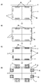
図5(A)、(B)は、本発明に係る有機EL表示装置の製造方法における小型基板形成工程の説明図である。図6(A)、(B)、(C)は、本発明に係る有機EL表示装置の製造方法において小型基板に保護フィルムを貼った状態の説明図である。図7(A)、(B)、(C)は、本発明に係る有機EL表示装置の製造方法における貼り合わせ工程の説明図である。図8(A)、(B)は、本発明に係る有機EL表示装置の製造方法における有機機能層形成工程の説明図である。
(Production method)
5A and 5B are explanatory views of a small substrate forming step in the method of manufacturing an organic EL display device according to the present invention. 6 (A), 6 (B), and 6 (C) are explanatory diagrams showing a state in which a protective film is attached to a small substrate in the method for manufacturing an organic EL display device according to the present invention. 7A, 7B, and 7C are explanatory diagrams of a bonding process in the method for manufacturing an organic EL display device according to the present invention. 8A and 8B are explanatory diagrams of the organic functional layer forming step in the method for manufacturing an organic EL display device according to the present invention.
有機EL表示装置1を製造するにあたって、本形態の小型基板形成工程は、図5(A)、(B)に示すように、TFT123、124などの回路素子、有機EL素子101の画素電極111、および隔壁112を小型基板2上に形成する工程からなる。
In manufacturing the organic
次に、小型基板2の一方面側21および他方面側22に保護フィルム6、7を貼着した後(保護フィルム貼着工程)、図6(B)の一点鎖線201で示す切断線に沿ってレーザ光を照射して、保護フィルム6、7と共に小型基板2を切断し洗浄する(レーザ切断工程)。これにより、小型基板2の切断面が基板面に対し垂直に調整される。また、小型基板2のレーザ切断は、図1(A)、(B)に示すように、小型基板2の複数の辺のうち少なくとも他の小型基板と隣接する2辺に対して行うことが良い。さらには、小型基板2の4隅にレーザ照射位置を示すアライメントマークを形成しておくことも良い。保護フィルム6、7は、いわゆるUVフィルムと称せられるもので、図6(C)に示すように、フィルム基板61、71と粘着材層63、73との間にUV剥離層62、72を備えている。
Next, after the
次に、貼り合わせ工程は、図7(A)に示すように、平坦な基準面を備えた定盤8に対して保護フィルム6を下に、定盤8上に複数枚の小型基板4を平面的に配列する。次に、保護フィルム7にUV光を照射して保護フィルム7を剥がす。その際、保護フィルム7は、粘着材層73も完全に除去される。そして、剥離面を洗浄する。次に、図7(B)に示すように、小型基板2の他方面(裏面)側22に、アクリル系などの接着剤30を塗布した後、小型基板2の他方面側22に大型基板3を重ね、接着剤30を硬化させる。その際、矢印Fで示すように、大型基板3に対して流体圧を印加して、大型基板3を定盤8に向けて押し付け、小型基板2と大型基板3との密着性を高めるとともに、複数枚の小型基板2の一方面側21の位置を合わせる。その結果、図7(C)に示すように、複数枚の小型基板2は、大型基板3に対して接着剤30を介して固定される。大型基板3に流体圧を印加する方法としては、ヘッドから大型基板3に向けて圧縮空気を噴出する方法がある。また、弾性を備えた隔膜を大型基板3に被せ、この隔膜によって仕切られた2つの空間のうち、大型基板3が配置されている側とは反対側の空間内に空気や液体などの流体を供給する方法でもよい。
Next, in the bonding step, as shown in FIG. 7A, the
次に、保護フィルム6に対してUV光を照射し、図8(A)、(B)に示すように、保護フィルム6を剥がした後、剥離面を洗浄する。保護フィルム6を剥がす際、粘着材層63も完全に除去される。
Next, the
次に、発光機能層形成工程は、図8(B)に一点鎖線で示すインクジェットヘッド9と小型基板2とを相対移動させながら行う。先ず、小型基板2上の隔壁112で囲まれた領域内に正孔注入/輸送層110aを構成する液状組成物を選択的に吐出、塗布した後、熱処理を行って正孔注入/輸送層110aを形成する。同様に、インクジェットヘッド9と小型基板2とを相対移動させながら、小型基板2上の隔壁112で囲まれた領域内に向けて、所定色に対応する発光層110bの液状組成物を吐出、塗布した後、熱処理を行って発光層110bを形成する。ここで、正孔注入/輸送層110aを形成するための液状組成物は、3,4−ポリエチレンジオキシチオフェン/ポリスチレンスルフォン酸(PEDOT/PSS)、ポリアニリン、ポリピロールなどの導電性高分子、MTDATA、フェニルアミン誘導体、銅フタロシアニンなどの溶液もしくは分散液である。また、発光層110bを形成するための液状組成物は、(ポリ)フルオレン誘導体(PF)、(ポリ)パラフェニレンビニレン誘導体(PPV)、ポリフェニレン誘導体(PP)、ポリパラフェニレン誘導体(PPP)、ポリビニルカルバゾール(PVK)、ポリチオフェン誘導体、ポリメチルフェニルシラン(PMPS)などのポリシラン系などの溶液もしくは分散液である。
Next, the light emitting functional layer forming step is performed while relatively moving the
次に図4(B)に示すように、蒸着法などにより、陰極12のカルシウム層12a、およびアルミニウム層12bを順次形成する。その際、広い面積に対して選択的にカルシウム層12a、およびアルミニウム層12bを形成することを目的に、端子形成領域などの外周部分を所定の部材で覆った状態で成膜を行う。
Next, as shown in FIG. 4B, a
次に、封止樹脂40を介して封止基板4を貼り付ける(封止工程)。それにより、図1(A)、(B)に示す有機EL表示装置1が製造される。なお、封止基板4に4枚の小型基板2よりも大きなものを用いる場合には、小型基板2の端子部分20に対応した外周部分を除く内側の領域のみ、封止樹脂40によって接着する。その後、封止基板4の外周部分をスクライブ装置を用いて切断し、小型基板2の端子形成領域20を露出させる。
Next, the sealing
(本形態の主な効果)
以上説明したように、本形態では、TFT123、124の形成や画素電極111の形成など、レーザアニールやフォトリソグラフィ技術が必要なプロセスは、大型基板4への貼り合せ工程の前に行う。また貼り合わせ工程の後、有機EL素子101の発光機能層110を形成する手段にインクジェット法を採用するので、任意の位置への材料塗布と成膜を容易に行うことができる。このため、有機EL素子101の発光機能層110を、複数枚の小型基板2を平面的に並べた広い領域に形成する場合でも、製造装置の大型化や歩留まりの低下が発生しない。
(Main effects of this form)
As described above, in this embodiment, processes that require laser annealing and photolithography techniques, such as the formation of the
また、本形態においては、貼り合わせ工程を行う前に、小型基板2の基板辺をレーザによって切断するレーザ加工を行うため切断面を直角にすることができ、有機EL表示装置1の小型基板2同士を高い位置精度をもって接合することができる。その結果、インクジェット法により発光機能層110を形成する際にも、小型基板2上の所定位置に高い位置精度で発光機能層110を形成することができる。
Further, in this embodiment, before performing the bonding step, the cutting surface can be made perpendicular because laser processing is performed to cut the substrate side of the
さらに、本形態では、小型基板2の一方面側(おもて面)21に保護フィルム6を貼着した状態で貼り合わせ工程を行うため、貼り合わせ工程で異物の付着や外力によるTFT123、124の損傷を防止できる。また、小型基板2の一方面側(おもて面)21を基準に大型基板3との貼り合わせを行うので、インクジェットヘッド9から複数の小型基板面への距離がいずれの小型基板2においても一定にできる。そのため、インクジェットヘッド9からの液滴の飛弾距離がいずれの小型基板2でも一定となり、飛弾距離のばらつきに起因する発光機能層110の形成位置や着弾粒のばらつきを防止することができ、精度の高い成膜をすることができる。
Furthermore, in this embodiment, the bonding process is performed in a state where the
また、小型基板2と大型基板3の貼り合わせ工程では、流体圧を大型基板3に加えて大型基板3を定盤8に押し付けるので、大型基板3および小型基板2に均一な力が加わる。従って、いずれの小型基板2も同一条件で貼り合せることができる。それ故、EL表示装置1の厚さ方向における小型基板2の位置ばらつきを防止でき、品位の高い画像を表示することができる。
In the bonding process of the
[実施の形態2]
図9(A)、(B)は、本発明の実施の形態2に係る有機EL表示装置の断面図、および画素領域の1つ分の断面構造を拡大して示す断面図である。なお、本形態の有機EL表示装置の基本的な構成は、実施の形態1と同様であるため、共通する機能を有する部分については、同一の符号を付してそれらの説明を省略する。
[Embodiment 2]
9A and 9B are a cross-sectional view of an organic EL display device according to
図9(A)、(B)において、本形態の有機EL表示装置1は、実施の形態1と同様、ボトムエミッション型であり、タイリング技術を利用した30インチ以上の大型表示装置として用いられる。すなわち、本形態の有機EL表示装置1は、4枚の小型基板2(TFTアレイ基板)が平面的に配列された状態で、その他方面側(裏面)22が透明な接着剤30を介して大型基板3に全面接着されている。また、小型基板2の一方面側(表面)21には、エポキシ樹脂などの封止樹脂40によって封止基板4が全面接着されている。ここで、接着剤30としては、小型基板2および大型基板3に用いたガラスと屈折率が略等しいアクリル系接着剤などが用いられる。本形態において、大型基板3は、小型基板3の複数枚分の大きさよりも大きい。これに対して、封止基板4は、小型基板2の複数枚分よりも小さく、小型基板2の一方面側21は、一部が封止基板4の端から張り出している。従って、小型基板2の一方面側21の端部に形成されている端子形成領域20に対して、フレキシブル配線基板(図示せず)などにより外部との電気的な接続を行うことができる。
9A and 9B, the organic
このように構成した有機EL表示装置1において、4枚の小型基板2の厚さ方向の位置がばらついた場合、あるいは小型基板2が面の外方向に傾いた場合には、各画素での発光位置がばらついてしまい、輝度むらが発生するなど、表示品位が低下する。そこで、本形態では、大型基板3と小型基板2との接着面に、小型基板2と大型基板3の基板間隔を制御する第1の基板間隔制御部材35を形成し、図7(A)、(B)、(C)同様の貼り合わせ工程で、小型基板2と大型基板3との間に第1の基板間隔制御部材35を介在させた状態で両基板を接着する。
In the organic
本形態において、第1の基板間隔制御部材35は、大型基板3に形成された突起であり、このような突起は、フォトリソグラフィ技術を用いて形成された柱状の感光性樹脂によって構成することができる。感光性樹脂としてはアクリル樹脂が知られている。また、第1の基板間隔制御部材35は、大型基板3に転写、印刷、あるいはインクジェット法により定着させた樹脂組成物であってもよい。この場合、樹脂組成物として、粒状あるいは棒状のギャップ材を樹脂に分散させたものを用いれば、所定高さの第1の基板間隔制御部材35を形成することができる。また、樹脂組成物として、粒状あるいは棒状のギャップ材を速乾性の樹脂に分散させたものを用いれば、大型基板3上で樹脂分が流動しないので、高さ寸法の精度が高い第1の基板間隔制御部材35を形成することができる。
In the present embodiment, the first substrate
これらいずれの方法で形成した場合も、第1の基板間隔制御部材35は大型基板3の所定位置に選択的に形成できる。従って、本形態では、有機EL素子101の形成領域と平面的に重なる領域を避けた領域、例えば、隔壁112や各種配線(図3に示す走査線131、信号線132、電源線133)と平面的に重なる領域に形成されている。その他の構成は実施の形態1と同様であるため説明を省略する。
In any case, the first substrate
以上説明したように、本形態では、貼り合せ工程において、小型基板2と大型基板3の間に、基板間隔を制御する第1の基板間隔制御部材35を介在させた状態で小型基板2と大型基板3を貼り合わせる。従って、小型基板2は、第1の基板間隔制御部材35によって大型基板3の表面を基準に位置間隔が高い精度で規定されるので、小型基板2の厚さ方向の間隔にばらつきが発生せず、かつ、小型基板2が面の外方向に傾くことがない。従って、大型基板3の側から表示光が出射されるボトムエミッション型表示の場合、各画素における発光位置を揃えることができるので、画面のゆがみが発生せず、表示品位の高い表示装置を提供できる。
As described above, in the present embodiment, in the bonding process, the
また、本形態において、第1の基板間隔制御部材35を、有機EL素子101の形成領域と平面的に重なる領域を避けた領域に形成しているため、本発明によるボトムエミッション型の有機EL表示装置1は、小型基板2と大型基板3との間に第1の基板間隔制御部材35が介在していても、表示光を遮ることがない。従って、表示品位の低下を抑えることができる。
Further, in this embodiment, the first substrate
なお、本形態では、第1の基板間隔制御部材35を大型基板3に形成した例を説明したが、小型基板2の方に形成してもよい。また、有機EL表示装置1がボトムエミッション型であっても、第1の基板間隔制御部材35の屈折率が、接着剤30、大型基板3、小型基板2の屈折率と略等しい場合には、有機EL素子101の形成領域と平面的に重なる領域に第1の基板間隔制御部材35を形成してもよい。
In the present embodiment, the example in which the first substrate
さらに、本形態の構成によれば、大型基板3に対する小型基板2の厚さ方向の位置にばらつきが発生せず、かつ、小型基板2が面の外方向に傾くことがない。従って、ボトムエミッション型およびトップエミッション型のいずれの有機EL表示装置1に本形態の構成を採用した場合も、インクジェットヘッド9からいずれの小型基板2への液滴の飛弾距離が一定となり、飛弾距離のばらつきに起因する発光機能層110の形成位置や着弾粒径のばらつきを防止することができる。そのため、輝度むらが発生しない品位の高い画像を表示することができるという効果を奏する。
Furthermore, according to the configuration of the present embodiment, the position in the thickness direction of the
[実施の形態3]
図10(A)、(B)は、本発明の実施の形態3に係る有機EL表示装置の断面図、および画素領域の1つ分の断面構造を拡大して示す断面図である。なお、本形態の有機EL表示装置の基本的な構成は、実施の形態1と同様であるため、共通する機能を有する部分については、同一の符号を付してそれらの説明を省略する。
[Embodiment 3]
10A and 10B are a cross-sectional view of an organic EL display device according to
図10(A)、(B)において、本形態の有機EL表示装置1は、実施の形態1と同様、ボトムエミッション型であり、タイリング技術を利用した30インチ以上の大型表示装置として用いられる。すなわち、本形態の有機EL表示装置1は、4枚の小型基板2(TFTアレイ基板)が平面的に配列された状態で、その他方面側(裏面)22が透明な接着剤30を介して大型基板3に全面接着されている。また、小型基板2の一方面側(表面)21には、エポキシ樹脂などの封止樹脂40によって封止基板4が全面接着されている。ここで、接着剤30は、小型基板2および大型基板3に用いたガラスと屈折率が略等しいアクリル系接着剤などが用いられている。本形態において、大型基板3は、小型基板3の複数枚分の大きさよりも大きい。これに対して、封止基板4は、小型基板2の複数枚分よりも小さく、小型基板2の一方面側21は、一部が封止基板4の端から張り出している。従って、小型基板2の一方面側21の端部に形成されている端子形成領域20に、フレキシブル配線基板(図示せず)などにより外部との電気的な接続を行うことができる。
10A and 10B, the organic
このように構成した有機EL表示装置1を製造するにあたり、本形態では、図7(A)、(B)、(C)で説明した貼り合わせ工程において、小型基板2と大型基板3との間に、基板間隔を制御する第1の基板間隔制御部材36を介在させ小型基板2と大型基板3とを接着する。
In manufacturing the organic
本形態において、第1の基板間隔制御部材36は、小型基板2と大型基板3との間に配置された粒状あるいは棒状のギャップ材である。このようなギャップ材からなる第1の基板間隔制御部材36を小型基板2と大型基板3との間に介在させるには、接着剤30の中に前記ギャップ材を予め分散させておけばよい。または、図7(B)に示すように配置した4枚の小型基板2の上に前記ギャップ材からなる第1の基板間隔制御部材36を散布する一方、大型基板3の表面に接着剤30を塗布し、しかる後に、小型基板2と大型基板3とを貼り合せてもよい。
In the present embodiment, the first substrate
ここで、前記ギャップ材は第1の基板間隔制御部材36としてその位置を制御できないので、ギャップ材にはその屈折率が接着剤30、大型基板3、小型基板2の屈折率と略等しい光学的に同質の材料を用いる。その他の構成は実施の形態1と同様であるため、説明を省略する。
Here, since the position of the gap material cannot be controlled as the first substrate
以上説明したように、本形態では、貼り合せ工程において、小型基板2と大型基板3の間に基板間隔を制御する第1の基板間隔制御部材36を介在させ小型基板2と大型基板3を貼り合わせる。従って、小型基板2は、第1の基板間隔制御部材36によって大型基板3の表面を基準に位置間隔が規定されるので、小型基板2の厚さ方向の間隔にばらつきが発生せず、かつ、小型基板2が面の外方向に傾くことがない。従って、大型基板3の側から表示光が出射されるボトムエミッション型表示の場合、各画素における発光位置を揃えることができるので、画面のゆがみが発生せず、表示品位の高い表示装置を提供できる。
As described above, in the present embodiment, in the bonding process, the
また、本形態に用いるギャップ材は、その屈折率が接着剤30、大型基板3、小型基板2の屈折率と略等しい光学的に同質の材料を用いる。この結果、ボトムエミッション型の有機EL表示装置1において、小型基板2と大型基板3との間にギャップ材が介在していても、表示品位の低下は生じない。
The gap material used in this embodiment is made of an optically homogeneous material whose refractive index is substantially equal to that of the adhesive 30, the
さらに、本形態の構成によれば、大型基板3に対する小型基板2の厚さ方向の位置間隔にばらつきが発生せず、かつ、小型基板2が面の外方向に傾くことがない。従って、インクジェットヘッド9からいずれの小型基板2への液滴の飛弾距離が一定となり、飛弾距離のばらつきに起因する発光機能層110の形成位置や着弾粒径のばらつきを防止することができる。そのため、輝度むらが発生しない品位の高い画像を表示することができる。
Furthermore, according to the configuration of the present embodiment, the position interval in the thickness direction of the
なお、本形態では、4枚の小型基板2の上にギャップ材を散布し、大型基板3の側に接着剤30を塗布したが、逆に大型基板2の上にギャップ材を散布し、小型基板2の側に接着剤30を塗布し、しかる後、小型基板2と大型基板3とを貼り合せてもよい。
In this embodiment, the gap material is spread on the four
なお、有機EL表示装置1がトップエミッション型の場合には、第1の基板間隔制御部材36として、屈折率が接着剤30、大型基板3、小型基板2の屈折率と相違するギャップ材を用いてもよい。
When the organic
[実施の形態4]
図11(A)、(B)は、本発明の実施の形態4に係る有機EL表示装置の断面図、および画素領域の1つ分の断面構造を拡大して示す断面図である。なお、本形態の有機EL表示装置の基本的な構成は、実施の形態1と同様であるため、共通する機能を有する部分については、同一の符号を付してそれらの説明を省略する。
[Embodiment 4]
11A and 11B are a cross-sectional view of an organic EL display device according to
図11(A)、(B)において、本形態の有機EL表示装置1は、実施の形態1と同様、ボトムエミッション型であり、タイリング技術を利用した30インチ以上の大型表示装置として用いられる。すなわち、本形態の有機EL表示装置1は、4枚の小型基板2(TFTアレイ基板)が平面的に配列された状態で、その他方面側(裏面)22が透明な接着剤30を介して大型基板3に全面接着されている。また、小型基板2の一方面側(表面)21には、エポキシ樹脂などの封止樹脂40によって封止基板4が全面接着されている。ここで、接着剤30は、小型基板2および大型基板3に用いたガラスと屈折率が略等しいアクリル系接着剤などが用いられている。本形態において、大型基板3は、小型基板3の複数枚分の大きさよりも大きい。これに対して、封止基板4は、小型基板2の複数枚分よりも小さく、小型基板2の一方面側21は、一部が封止基板4の端から張り出している。従って、小型基板2の一方面側21の端部に形成されている端子形成領域20に、フレキシブル配線基板(図示せず)などにより外部との電気的な接続を行うことができる。
11A and 11B, the organic
本形態の有機EL表示装置1は、実施の形態2と同様、大型基板3と小型基板2との接着面に、小型基板2と大型基板3との基板間隔を制御する第1の基板間隔制御部材35を形成しておき、図7(A)、(B)、(C)で説明した貼り合わせ工程では、小型基板2と大型基板3の間に第1の基板間隔制御部材35を介在させた状態で接着する。第1の基板間隔制御部材35は、大型基板3あるいは小型基板2に形成された突起であり、このような突起は、フォトリソグラフィ技術を用いて形成された柱状の感光性樹脂によって構成することができる。また、第1の基板間隔制御部材35は、大型基板3に転写、印刷、あるいはインクジェット法により定着させた樹脂組成物であってもよい。
Similar to the second embodiment, the organic
さらに本形態では、封止基板4と小型基板2の接着面に、小型基板2と封止基板4の基板間隔を制御する第2の基板間隔制御部材45を形成しておき、エポキシ樹脂などの封止樹脂40によって、小型基板2と封止基板4との間に、第2の基板間隔制御部材45を介在させた状態で両者を接着する。
Further, in the present embodiment, a second substrate
本形態において、第2の基板間隔制御部材45は、封止基板4に形成された突起であり、このような突起は、フォトリソグラフィ技術を用いて形成された柱状の感光性樹脂によって構成することができる。また、第2の基板間隔制御部材45は、封止基板4に転写、印刷、あるいはインクジェット法により定着させた樹脂組成物であってもよい。この場合、樹脂組成物として、粒状あるいは棒状のギャップ材を樹脂に分散させたものを用いれば、所定高さの第2の基板間隔制御部材45を形成することができる。また、樹脂組成物として、粒状あるいは棒状のギャップ材を速乾性の樹脂に分散させたものを用いれば、封止基板4上で樹脂分が流動しないので、高さ寸法の精度が高い第2の基板間隔制御部材45を形成することができる。
In this embodiment, the second substrate
これらいずれの方法で形成した場合も、第2の基板間隔制御部材45は封止基板4の所定位置に選択的に形成できる。従って、本形態では、有機EL素子101の形成領域と平面的に重なる領域を避けた領域、例えば、隔壁112や各種配線(図3に示す走査線131、信号線132、電源線133)と平面的に重なる領域に形成されている。その他の構成は、実施の形態1と同様であるため、説明を省略する。
When formed by any of these methods, the second substrate
以上説明したように、本形態では、実施の形態2と同様、貼り合せ工程において、小型基板2と大型基板3との間の基板間隔を制御する第1の基板間隔制御部材35を介在させた状態で小型基板2と大型基板3とを貼り合わせる。従って、小型基板2は、第1の基板間隔制御部材35によって大型基板3を基準に位置間隔が規定されるので、小型基板2の厚さ方向の位置にばらつきが発生せず、かつ、小型基板2が面の外方向に傾くことのない。従って、大型基板3の側から表示光が出射されるボトムエミッション型の場合、各画素における発光位置を揃えることができるので、画面のゆがみが発生せず、表示品位の高い表示装置を提供できる。
As described above, in the present embodiment, as in the second embodiment, the first substrate
また、本形態の構成によれば、大型基板3に対して小型基板2の厚さ方向の間隔にばらつきが発生せず、かつ、小型基板2が面の外方向に傾くことがない。従って、ボトムエミッション型およびトップエミッション型のいずれの有機EL表示装置1に本形態の構成を採用した場合にも、インクジェットヘッド9からの液滴の飛弾距離がいずれの小型基板2へも一定となり、飛弾距離のばらつきに起因する発光機能層110の形成位置や着弾粒径などのばらつきを防止できる。そのため、輝度むらが発生しない品位の高い画像を表示することができるという実施の形態2と同様な効果を有する。
In addition, according to the configuration of the present embodiment, there is no variation in the distance in the thickness direction of the
また、トップエミッション型の有機EL表示装置1に本形態の構成を採用すれば、小型基板2と封止基板4との間に第2の基板間隔制御部材45を介在させた状態で両者を接着するため、4枚の小型基板2は、封止基板4に対して高い位置精度で貼り合わされる。従って、各画素における発光位置を揃えることができるので、表示品位の向上を図ることができる。しかも、第2の基板間隔制御部材45を、有機EL素子101の形成領域と平面的に重なる領域を避けた領域に形成するため、トップエミッション型の有機EL表示装置1において、小型基板2と大型基板3の間に第2の基板間隔制御部材45が介在していても、表示光を遮ることがない。従って、表示品位の低下を抑えることができる。
If the configuration of this embodiment is adopted for the top emission type organic
さらには、封止基板4の端部をスクライブ装置等を用いて切断し、小型基板2上の端子領域を露出させる際に、小型基板2と封止基板4とが高い位置精度をもって貼り合わせてあるので、封止基板4を正確に切断することができる。
Furthermore, when the end portion of the sealing
さらにまた、第2の基板間隔制御部材45を、有機EL素子101の形成領域と平面的に重なる領域を避けて形成しているため、小型基板2と封止基板4との間に第2の基板間隔制御部材45が介在していても、封止基板4からの応力が第2の基板間隔制御部材45を介して有機EL素子101に加わらない。従って、有機EL素子101が損傷しないので、有機EL表示装置1の信頼性を向上することができる。
Furthermore, since the second substrate
なお、本形態では、実施の形態2と同様、小型基板2と大型基板3との間に突起状の第1の基板間隔制御部材35を介在させたが、実施の形態3で説明した粒状、棒状のギャップ材を用いた第1の基板間隔制御部材36を介在させてもよい。
In the present embodiment, as in the second embodiment, the protruding first substrate
[実施の形態5]
図12(A)、(B)は、本発明の実施の形態5に係る有機EL表示装置の断面図、および画素領域の1つ分の断面構造を拡大して示す断面図である。なお、本形態の有機EL表示装置の基本的な構成は、実施の形態1と同様であるため、共通する機能を有する部分については、同一の符号を付してそれらの説明を省略する。
[Embodiment 5]
12A and 12B are a cross-sectional view of an organic EL display device according to Embodiment 5 of the present invention and a cross-sectional view showing an enlarged cross-sectional structure of one pixel region. In addition, since the basic structure of the organic EL display device of this embodiment is the same as that of
図12(A)、(B)において、本形態の有機EL表示装置1は、実施の形態1と同様、ボトムエミッション型であり、タイリング技術を利用した30インチ以上の大型表示装置として用いられる。すなわち、本形態の有機EL表示装置1は、4枚の小型基板2(TFTアレイ基板)が平面的に配列された状態で、その他方面側22が透明な接着剤30を介して大型基板3に全面接着されている。また、小型基板2の一方面側(おもて)21には、エポキシ樹脂などの封止樹脂40によって封止基板4が全面接着されている。ここで、接着剤30としては、小型基板2および大型基板3として用いたガラスと屈折率が略等しいアクリル系接着剤などが用いられている。本形態において、大型基板3は、小型基板3の複数枚分の大きさよりも大きい。これに対して、封止基板4は、小型基板2の複数枚分よりも小さく、小型基板2の一方面側21は、一部が封止基板4の端から張り出している。従って、小型基板2の一方面側21の端部に形成されている端子形成領域20に対して、フレキシブル配線基板(図示せず)などにより外部との電気的な接続を行うことができる。
12A and 12B, the organic
本形態の有機EL表示装置1では、実施の形態2と同様、大型基板3と小型基板2の接着面に対して、小型基板2と大型基板3との基板間隔を制御する第1の基板間隔制御部材35を形成しておき、図7(A)、(B)、(C)同様の貼り合わせ工程では、小型基板2と大型基板3との間に第1の基板間隔制御部材35を介在させた状態で両基板を接着する。このような第1の基板間隔制御部材35は、大型基板3に形成された突起であり、このような突起は、例えば、フォトリソグラフィ技術を用いて形成された柱状の感光性樹脂によって構成することができる。また、第1の基板間隔制御部材35は、大型基板3に転写、印刷、あるいはインクジェット法により定着させた樹脂組成物であってもよい。
In the organic
また、本形態では、小型基板2と封止基板4との間に基板間隔を制御する第2の基板間隔制御部材46を配置しておき、エポキシ樹脂などの封止樹脂40によって、この第2の基板間隔制御部材46を介在させたまま両者を接着する。
In the present embodiment, a second substrate
本形態では、第2の基板間隔制御部材46は、小型基板2と封止基板4の間に配置された粒状あるいは棒状のギャップ材である。このようなギャップ材からなる第2の基板間隔制御部材46を小型基板2と封止基板4との間に介在させるには、封止樹脂40の中にギャップ材を分散させておく方法がある。また、封止基板4を貼り合せる封止工程で、4枚の小型基板2の上にギャップ材を散布し、また一方の封止基板4に封止樹脂40を塗布し、しかる後に、小型基板2と封止基板4とを貼り合せてもよい。さらにはその逆に、封止基板4にギャップ材を撒き、小型基板2側に封止樹脂を塗布して接着しても良い。その他の構成は、実施の形態1と同様であるため、説明を省略する。
In the present embodiment, the second substrate
以上説明したように、本形態では、実施の形態2と同様、貼り合せ工程において、小型基板2と大型基板3の基板間隔を制御する第1の基板間隔制御部材35を介在させた状態で小型基板2と大型基板3とを貼り合わせる。従って、小型基板2は、第1の基板間隔制御部材35によって大型基板3を基準に位置間隔が規定されるので、小型基板2の厚さ方向の間隔にばらつきが発生せず、かつ、小型基板2が面の外方向に傾くことがない。従って、大型基板3の側から表示光が出射されるボトムエミッション型の場合、各画素における発光位置を揃えることができるので、画面のゆがみの無い表示品位の高い表示装置を提供できる。
As described above, in the present embodiment, in the same manner as in the second embodiment, in the bonding process, the first substrate
また、本形態の構成によれば、大型基板3に対して小型基板2の厚さ方向の位置にばらつきが発生せず、かつ、小型基板2が面の外方向に傾くことがない。従って、ボトムエミッション型およびトップエミッション型表示のいずれの有機EL表示装置1に本形態の構成を採用した場合も、インクジェットヘッド9からいずれの小型基板2への液滴の飛弾距離が一定であるので、飛弾距離のばらつきに起因する発光機能層110の形成位置や着弾粒径のばらつきを防止することができる。そのため、輝度むらが発生しない品位の高い画像を表示することができるという効果を奏する。
Further, according to the configuration of the present embodiment, there is no variation in the position of the
さらに、トップエミッション型の有機EL表示装置1に本形態の構成を採用すれば、小型基板2と封止基板4の間に第2の基板間隔制御部材46を介在させた状態で両者を接着するため、4枚の小型基板2は、封止基板4に対して高い間隔精度で貼り合わされている。従って、各画素における発光位置を揃えることができるので、画面にゆがみの無い表示品位の高い画像を得ることができる。但し、ギャップ材を用いた基板間隔制御では、その位置を正確に制御できないので、ギャップ材の屈折率が封止樹脂40、封止基板4、小型基板2の屈折率と略等しい材料を用いれば、ギャップ材に起因する表示品位の低下を防止できる。
Furthermore, if the configuration of the present embodiment is adopted in the top emission type organic
さらには、封止基板4の端部をスクライブ装置等を用いて切断し、小型基板2上の端子領域を露出させる際に、小型基板2と封止基板4とが高い位置精度をもって貼り合わせてあるので、封止基板4を正確に切断することができる。
Furthermore, when the end portion of the sealing
なお、本形態では、実施の形態2と同様、小型基板2と大型基板3との間に突起状の第1の基板間隔制御部材35を介在させたが、実施の形態3で説明した粒状あるいは棒状の第1の基板間隔制御部材36を用いてもよい。
In the present embodiment, as in the second embodiment, the protruding first substrate
[実施の形態6]
図13(A)、(B)は、本発明の実施の形態6に係る有機EL表示装置の製造方法を用い、小型基板の作製を終了した段階の説明図である。図14(A)〜(D)および図15(A)〜(F)は、図1に示す有機EL表示装置の製造方法を示す工程断面図である。なお、本形態の有機EL表示装置の基本的な構成は、実施の形態1と同様であるため、共通する機能を有する部分については、同一の符号を付してそれらの説明を省略する。
[Embodiment 6]
FIGS. 13A and 13B are explanatory diagrams at the stage where the fabrication of the small substrate is completed using the method for manufacturing an organic EL display device according to
有機EL表示装置1を製造するにあたって、本形態では、図13(A)、(B)に示すように、先ずTFT123、124などの回路素子、有機EL素子101の画素電極111、および隔壁112等を、小型基板2上に形成する。この工程では、電気光学装置用基板2は、薄型化する前の厚いガラス基板2’であり、その厚さが例えば0.5mmある。
In manufacturing the organic
次に、図13(A)、(B)および図14(A)に示すように、小型基板2の一方面側(おもて)21に保護フィルム6を貼着する(保護フィルム貼着工程)。保護フィルム6は、いわゆるUVフィルムと称せられるもので、図13(B)に示すように、フィルム基板61と粘着材層63との間にUV剥離層62を備えている。保護フィルム6は、小型基板2の一方面側21の端子20が形成されている領域を除くように貼ってもよく、小型基板2の全面を覆ってもよい。また、小型基板2については、レーザ光を照射して、保護フィルム6とともに切断し、基板の外形を調整することがよい。小型基板2のレーザ切断は、基板の複数の辺のうち、少なくとも、図1(A)、(B)に示すように配列した状態で他の小型基板2と隣接する辺に対して行う。また、基板2の4隅にレーザの照射位置を示すアライメントマークを形成しておくことが好ましい。このようなレーザ切断を行うと、有機EL表示装置1を組み立てた状態で小型基板2同士を高い位置精度をもって接合できる。また、後述する研磨時にチップが発生することを防止できる。
Next, as shown to FIG. 13 (A), (B) and FIG. 14 (A), the
次に、図14(C)に示す研磨装置200において、小型基板2の薄型化を行う。それには、まず、基板2を複数枚、研磨装置200の定盤210上に並べて固定する(固定工程)。この研磨装置200は、被研磨基板が配置される部分に凹部220が形成されたセラミックス製の定盤210を備えており、この凹部220内には、ワックス250が充填されている。従って、定盤を通して間接的に、あるいは、直接的にワックス250を約摂氏80度の温度まで加熱して溶融させた後、溶融したワックス250の表面に、基板の一方面側21を向けて複数枚平面的に配置する。この後、配列した基板2に流体圧をかけ凹部220に押し付ける。それには、ヘッドから基板2に向けて圧縮空気を噴出するか、あるいは、弾性を備えた隔膜を基板2に被せ、この隔膜によって仕切られた2つの空間のうち、基板2が配置されている側とは反対の空間に、空気や液体などの流体を供給すればよい。このようにすると小型基板2の各々に均一な力をかけることができる。
Next, in the
次に、溶融しているワックス250を摂氏25度の温度まで自然冷却、あるいは強制冷却し、ワックス250を固化させる。その結果、図14(C)に示すように、基板2は、他方面側22を上に向けて、定盤210の凹部220にワックス250で固定される。
Next, the
次に、基板の薄型化を行う。それには、研磨用ヘッド280を基板2の上方に配置し、ヘッド280を軸線周りに回転させると同時に、ヘッド280とは異なる速度で定盤210も回転させる。また、研磨用ヘッド280と基板2との間には砥粒の懸濁液を供給し、同時に、矢印Pで示す方向に約150g/cm2程度の荷重をかける。これによって、基板2の表面を約7.2μm/分の速度で研磨し、始めの厚さ0.5mmから25μmの厚さにまで薄型化する(ラッピング工程)。
Next, the substrate is thinned. For this purpose, the polishing
次に、ポリッシング工程は、図14(D)に示すように、研磨用ヘッド280の下部に柔らかい研磨布281を取り付け、研磨用ヘッド280と基板2との間に砥粒の懸濁液を必要に応じて供給し、同時に矢印Pで示す方向に約50g/cm2程度の荷重をかけ、先にラッピングした面を平滑化する。それにより小型基板2は、ガラスと同等の光透過率を有することになる。
Next, in the polishing step, as shown in FIG. 14D, a
次に、図15(A)に示すように、小型基板2の他方面側(研磨面)22を洗浄する。次に、図15(B)に示すように、小型基板2の他方面側22に接着剤30を塗布した後、図15(C)に示すように小型基板2の他方面側22に大型基板3を重ね、接着剤30を硬化させる。その際も、大型基板3に対して流体圧を印加して大型基板3を定盤210方向に押し付け、両基板の密着性を高める。大型基板3に対して流体圧を印加する方法は、例えば、ヘッドから大型基板3に向けて圧縮空気を噴出する。あるいは、弾性を備えた隔膜を大型基板3に被せ、この隔膜によって仕切られた2つの空間のうち、大型基板3が配置されている側とは反対側の空間に空気や液体などの流体を供給してもよい。
Next, as shown in FIG. 15A, the other surface side (polishing surface) 22 of the
このようにして、定盤210上で複数枚の小型基板2を大型基板3に貼り合わせ貼り合わせ基板10とした後、固化していたワックス250を定盤210を介して間接的に、あるいは直接的に、摂氏約80度の温度にまで加熱して溶融させ、図15(D)に示すように小型基板2(貼り合わせ基板10)を定盤210の凹部220から取り外す。
In this way, a plurality of
次に、保護フィルム6にUV光を照射し、図15(E)に示すように保護フィルム6を剥がす。この時、粘着材層63も基板2の一方面側21から完全に除去される。次に、貼り合わせ基板10の洗浄を行う。
Next, the
このようにして、図8(A)に示す貼り合わせ基板10を作製した後、発光機能層の形成を行う。以下の工程は、本発明の実施の形態1と同様であるので、ここでは説明を省略する。このようにして作製された有機EL発光機能層を有する基板10を、図15(F)に示すように封止樹脂40を介して封止基板4に貼り付けモジュール1’を構成する。このモジュール1’を用いて図1(A)、(B)に示す有機EL表示装置1を製造する。
In this manner, after the bonded
なお、大型基板3、封止基板4についてもレーザを照射して切断し、所定のサイズに調整することができる。また、図15(E)、(F)に示す状態にように、複数枚の小型基板2と大型基板3を貼り合わせて貼り合わせ基板10とした後、あるいは、電気光学装置用基板2を挟みこむように大型基板3および封止基板40を積層してモジュール1’とした後、封止基板4あるいは大型基板3に研磨を施し薄型化してもよい。この場合も、図14(B)、(C)、(D)に示す研磨装置200を用い、貼り合わせ基板10あるいはモジュール1’をワックス250により定盤210に固定し、しかる後、前記したラッピング工程およびポリッシング工程を行えばよい。
The
(本形態の主な効果)
以上説明したように、本形態では、小型基板2に所定の工程を施した後薄型化するため、薄型化の前の工程までは厚い小型基板2のまま取り扱える。このため、小型基板2にガラスなどの硬質基板を用い、かつ、この基板を例えば100μm以下、さらには、50μm以下にまで薄型化した場合でも、基板が割れるおそれがない。しかも、複数枚の小型基板2を一括して研磨するので効率がよい。
(Main effects of this form)
As described above, in this embodiment, since the
また、小型基板2の薄型化を、化学エッチングではなく機械的研磨により行うので、小型基板2の表面が荒れることがない。しかも、小型基板2に形成された多数の端子20がある場合でも、反対側を選択的に研磨できるので端子20が損傷することがない。
Further, since the
さらに、溶融していたワックスを固化させるだけで小型基板2を定盤210上に固定することができ、研磨が終了した後はワックス250を溶融させるだけで電気光学装置用基板2を定盤210から取り外すことができる。しかも、ワックス250による固定であれば、固定するための応力が電気光学装置2の一部分に集中することがないので基板が割れることもない。
Furthermore, the
さらに、研磨により複数枚の小型基板2の表面が揃うので定盤210上で複数枚の小型基板2と大型基板3とを容易に、かつ、高い精度で貼り合わせることができる。
Furthermore, since the surfaces of the plurality of
また、本形態では、TFT123、124の形成、画素電極111の形成など、レーザアニールやフォトリソグラフィ技術が必要なプロセスについては、大型基板4への貼り合わせ工程の前に行い、その後有機EL素子101の発光機能層形成には、任意の位置への塗布を容易に行うことのできるインクジェット法を採用できる。このため、発光機能層110を複数枚の小型基板2を平面的に並べた広い領域に形成する場合でも、製造装置の大型化や歩留まりの低下が発生しない。
In this embodiment, processes that require laser annealing and photolithography techniques, such as the formation of
また、本形態においては、貼り合わせ工程を行う前に小型基板2の基板辺をレーザにより切断するため、有機EL表示装置1を組み立てた状態で小型基板2同士を高い位置精度をもって接合できる。従って、インクジェット法により発光機能層110を形成する際、小型基板2上の所定位置に高い精度をもって発光機能層110を形成することができる。
Moreover, in this embodiment, since the substrate side of the
さらに、本形態では、小型基板2の一方面側21に保護フィルム6を貼着した状態で貼り合わせ工程を行うため、薄型化工程や貼り合わせ工程の際、異物の付着や外力によるTFT123、124などの損傷を防止できる。また、異物の付着や損傷などが発生しない。
Furthermore, in this embodiment, since the bonding process is performed in a state where the
また、小型基板2の保護フィルム6が形成されている面21を基準に大型基板3との貼り合わせを行うので、インクジェット法により発光機能層110を形成する際、インクジェットヘッド9から液滴の飛弾距離がいずれの小型基板2でも一定であるので、飛弾距離のばらつきに起因する発光機能層110の形成位置や粒径などのばらつきを防止することができ、品位の高い画像を表示することができる。
Further, since the surface of the
また、貼り合わせ工程では、流体圧を大型基板3に加えて大型基板3を定盤210に押し付け、小型基板2と大型基板3とを貼り合わせるので、大型基板3および小型基板2に均一な力が加わわり、いずれの小型基板2も同一条件で貼り合わせることができる。そのため、EL表示装置1を形成した小型基板2の厚さ方向における位置ばらつきなどを防止し、画面にゆがみの無い品位の高い画像を表示することができる。
Further, in the bonding process, fluid pressure is applied to the
[実施の形態7]
図16(A)、(B)は、本発明の実施の形態7に係る有機EL表示装置の製造方法を用い、小型基板の作製を終了した段階の説明図である。図17(A)〜(E)は、図1に示す有機EL表示装置の製造工程のうち、パネルを薄型化する工程を示す工程断面図である。図18(A)〜(D)は、図1に示す有機EL表示装置の製造工程のうち、パネルを薄型化するとともに端子にフレキシブル配線基板を接続する工程を示す説明図である。なお、本形態の有機EL表示装置の基本的な構成は、実施の形態1と同様であるため、共通する機能を有する部分については、同一の符号を付してそれらの説明を省略する。
[Embodiment 7]
FIGS. 16A and 16B are explanatory diagrams at the stage where the fabrication of the small substrate is completed using the method for manufacturing an organic EL display device according to
有機EL表示装置1を製造するにあたって、本形態では、図16(A)、(B)に示すように、先ずTFT123、124などの回路素子、有機EL素子101の画素電極111、および隔壁112等を小型基板2上に形成する。この工程では、電気光学装置用基板2は薄型化する前の厚いガラス基板2’であり、その厚さが例えば0.5mmある。
In manufacturing the organic
次に、図16(A)、(B)に示すように、小型基板2の一方面側(おもて)21に保護フィルム6を貼着する(保護フィルム貼着工程)。本形態では、保護フィルム6は、小型基板2の全面を覆うように貼られている。また、小型基板2はレーザ光を照射して保護フィルム6とともに切断し、基板の外形を調整することがよい。小型基板2のレーザ切断は、基板の複数の辺のうち少なくとも図1(A)、(B)に示した配列の状態で他の小型基板2と隣接する辺に対して行う。
Next, as shown to FIG. 16 (A), (B), the
次に、図14(C)に示す研磨装置200を用いて小型基板2’の薄型化を行う。薄型化工程は実施形態6の図14に従う。薄型化の終わった複数枚の小型基板2は、実施形態6の図15の工程により大型基板3に張り合わされ、しかる後、実施形態1の発光機能層の形成を行う。これらの製造工程および製造方法は、本発明の実施の形態6および1と同様であり、詳細は既に説明されているのでここでは説明を割愛する。
Next, the
次に、図17(A)に示すように複数の小型基板2と同等、あるいはそれよりも大きな封止基板4を、封止樹脂40を介して小型基板2の一方面側21に貼り付けパネル1’を形成する。この段階では小型基板2に形成されている端子20は、封止基板4で覆われた状態にある。
Next, as shown in FIG. 17A, a sealing
次に、図17(B)の研磨装置200においてパネル1’に対する薄型化を行う。パネル1’は、まず図17(B)に示すように、封止基板4を上向きにして研磨装置200の定盤210上に固定する(固定工程)。この工程は定盤210を介して間接的、あるいは直接的に、ワックス250を摂氏約80度の温度にまで加熱して溶融させた後、溶融したワックス250の表面に大型基板3を下にパネル1’を配置し、パネル1’に流体圧を印加して定盤の凹部220に押し付ける。その際、ヘッドからパネル1’に向けて圧縮空気を噴出する。または、弾性を備えた隔膜をパネル1’に被せ、この隔膜によって仕切られた2つの空間のうちパネル1’が配置されている側とは反対側の空間に空気や液体などの流体を供給すればよい。このようにすると、小型基板2の各々に均一な力をかけることができる。
Next, the
次に、溶融しているワックス250を摂氏25度の温度にまで自然冷却、あるいは強制冷却し、ワックス250を固化させる。
Next, the melted
次に、パネルの薄型化を行う。それには、研磨用ヘッド280をパネル1’の上方に配置し、そこで研磨用ヘッド280を軸線周りに回転させ、かつ、研磨用ヘッド280と異なる速度で定盤210も回転させる。この状態で、研磨用ヘッド280とパネル1’との間に砥粒の懸濁液を供給し、かつ、矢印Pで示す方向に約150g/cm2程度の荷重をかける。これによって基板2の表面を約7.2μm/分の速度で研磨し、始めの厚さ0.5mmから25μmの厚さにまで薄型化できる(ラッピング工程)。
Next, the panel is thinned. For this purpose, the polishing
次に、ポリッシング工程は、図17(C)に示すように、研磨用ヘッド280の下部に柔らかい研磨布281を取り付け、研磨用ヘッド280とパネル1’との間に砥粒の懸濁液を必要に応じて供給し、同時に矢印Pで示す方向に約50g/cm2程度の荷重をかけ、先にラッピングした面を平滑化する。それにより、小型基板2は、ガラスと同等の光透過率を有することになる。
Next, in the polishing step, as shown in FIG. 17C, a
しかる後に、固化していたワックス250を定盤210を介して間接的に、あるいは直接的に摂氏約80度の温度にまで加熱して溶融させ、パネル1’を定盤210から取り外す。
Thereafter, the solidified
また、大型基板3についても薄型化する場合には、図17(B)、(C)と同様に図17(D)に示すように、大型基板3を上向きにしてパネル1’を研磨装置200の定盤210上に固定した後、大型基板3の表面を研磨して大型基板3を0.5mmから25μmの厚さにまで薄型化する(ラッピング工程)。次に、図17(E)に示すように大型基板3の表面を平滑化し(ポリッシング工程)、しかる後パネル1’を定盤210から取り外す。(図18(A))
Further, in the case where the
次に、パネル1’を洗浄した後、図18(B)に示すように大型基板3にレーザを照射して端部を切断し、大型基板3を所定のサイズに調整する。
Next, after cleaning the
次に、図18(C)に示すように封止基板4にレーザを照射して端子20の上方部分を切断し、封止基板4を所定のサイズに調整する。その結果、小型基板2に形成されていた端子20が露出する。そして、図18(D)に示すように端子20に、IC70がCOF実装されたフレキシブル配線基板7を接続する。
Next, as shown in FIG. 18C, the sealing
(本形態の主な効果)
以上説明したように、本発明では、パネルの薄型化を図るにあたって小型基板と封止基板を貼り合せた後の工程で薄型化する。このため封止基板としてガラス材を用い、かつ、この封止基板を例えば100μm以下、さらには、50μm以下にまで薄型化した場合でも、製造工程中に対向基板が割れるおそれはない。また、薄型化の方法に化学エッチングではなく研磨法を用いるので、小型基板に形成されている端子がエッチングされることはない。さらには研磨の際、端子は封止基板で覆われているので端子が損傷することもない。さらに端子出しは、研磨後の封止基板を切断することによって容易に行える。
(Main effects of this form)
As described above, in the present invention, in order to reduce the thickness of the panel, the panel is thinned in a process after the small substrate and the sealing substrate are bonded together. Therefore, even when a glass material is used as the sealing substrate and the sealing substrate is thinned to, for example, 100 μm or less, and further to 50 μm or less, there is no possibility that the counter substrate is broken during the manufacturing process. In addition, since the polishing method is used instead of the chemical etching for the thinning method, the terminals formed on the small substrate are not etched. Furthermore, since the terminal is covered with the sealing substrate during polishing, the terminal is not damaged. Further, the terminal can be easily formed by cutting the polished sealing substrate.
また、上記固定工程ではパネル1’に流体圧を加えて定盤210に固定するため、パネル1’全体に均一な力をかけることができる。従って、パネル1’を適正な姿勢で定盤210上に固定することができ、高い精度での研磨を行うことができる。
In the fixing step, fluid pressure is applied to the panel 1 'to fix it to the
さらにまた研磨の際、パネル1’をワックス250で定盤210上に固定するので、研磨が終了した後、ワックス250を溶融させるだけでパネル1’を定盤210から取り外すことができる。しかも、ワックス250による固定であれば、固定するための応力がパネル1’の一部分に集中することがないのでパネル1’が割れることもない。また、ワックス250であれば約80度の温度で溶融するので、たとえパネル1’が有機EL材料を保持していたとしても有機EL材料が劣化しない。
Furthermore, since the
[実施の形態1の変形例]
図19に示すように、図6、図13、図16に示す工程で用いる保護フィルム6として、フィルム基材61に隔壁112の高さよりも厚い粘着剤層63を用いれば、図19に示すように、保護フィルム6を小型基板2の一方面側21に貼った際、小型基板2と保護フィルム6との間への気泡の侵入を防止できる。従って、保護フィルム6の表面の気泡に起因する凹凸が発生しないので、小型基板2と大型基板3を貼り合わせる際に、小型基板2の一方面側21の位置を高い精度で揃えることができる。その結果、インクジェット法により、発光機能層110を安定して形成することができるとともに、有機EL表示装置1を構成した状態において小型基板2の厚さ方向における位置(高さ)ばらつきを防止できる。従って、本発明に夜表示装置は、品位の高い画像を表示することができる。
[Modification of Embodiment 1]
As shown in FIG. 19, if the
また、図20(A)に示すように、保護フィルム6に、発光機能層110を形成するための液状組成物に対する撥液材層64を追加し、かつ、粘着剤層63を隔壁112の高さよりも薄くしておけば、保護フィルム6を除去した後、図20(B)に示すように、液状組成物の塗布領域の周囲、すなわち、隔壁112の上端部に撥液材層64を転写することができる。従って、小型基板2の一方面側21に対して、フッ素化合物を用いたプラズマ処理などの格別な撥液処理を行わなくてもよいので、製造工程の簡素化を図ることができる。
In addition, as shown in FIG. 20A, a liquid
なお、上記形態では有機EL表示装置1を例にとったが、他の自発光型素子を用いた自発光型電気光学装置の製造に本発明を適用してもよい。
In the above embodiment, the organic
[電子機器への適用]
本発明を適用した電気光学装置は、30インチを越えるような大画面を備えた電子機器に搭載されることが最も好ましい。しかし、同様の製造方法あるいは技術思想によった大小の表示装置に適用できることは云うまでも無い。
[Application to electronic devices]
The electro-optical device to which the present invention is applied is most preferably mounted on an electronic apparatus having a large screen exceeding 30 inches. However, it goes without saying that the present invention can be applied to large and small display devices based on the same manufacturing method or technical idea.
1 有機EL表示装置(電気光学装置)、2 小型基板(TFTアレイ基板)、3 大型基板、4 封止基板、6、7 保護フィルム、8 定盤、9 インクジェットヘッド、35、36 第1の基板間隔制御部材、45、46 第2の基板間隔制御部材、101 有機EL素子、110 発光機能層、111 画素電極、123、124 TFT。
DESCRIPTION OF
Claims (25)
小型基板の一方面に、前記画素スイッチング用素子、前記自発光素子の画素電極、及び液状組成物の塗布領域を規定する隔壁を形成する小型基板形成工程と、
前記小型基板形成工程の後、前記小型基板の少なくとも前記一方面側に、前記隔壁の高さよりも薄い粘着剤層と前記液状組成物に対する撥液材層とをフィルム基材の一方面側に形成した保護フィルムを貼着する工程と、
前記保護フィルムの側を定盤に向けて前記複数枚の小型基板を配列し、前記定盤上に配列させた前記複数枚の小型基板の前記他方面側に前記大型基板を重ね、この状態で、流体圧を前記大型基板に加えて当該大型基板を前記定盤に向けて押し付けて、前記複数枚の小型基板の前記他方面側と前記大型基板とを貼り合わせる、貼り合わせ工程と、
前記貼り合わせ工程を行った後、前記保護フィルムを前記小型基板の前記一方面側から除去することにより、前記液状組成物の塗布領域の周囲に前記撥液材層を前記小型基板側に転写する工程と、
前記複数枚の小型基板の前記塗布領域に対してインクジェット法により液状組成物を選択的に塗布して、前記自発光素子の発光機能層を形成する発光機能層形成工程と、を有することを特徴とする電気光学装置の製造方法。 In a method for manufacturing an electro-optical device in which a plurality of substrates each including a pixel switching element and a self-light-emitting element are arranged in a plane in each of a large number of pixel regions arranged in a matrix,
A small substrate forming step of forming, on one surface of the small substrate , the pixel switching element, the pixel electrode of the self-luminous element, and a partition defining a coating region of the liquid composition ;
After the small substrate forming step, an adhesive layer thinner than the height of the partition and a liquid repellent material layer for the liquid composition are formed on one surface side of the film substrate on at least the one surface side of the small substrate. Attaching the protective film made ,
The plurality of small substrates are arranged with the side of the protective film facing the surface plate, and the large substrate is stacked on the other surface side of the plurality of small substrates arranged on the surface plate, A bonding step in which fluid pressure is applied to the large substrate and the large substrate is pressed against the surface plate to bond the other surface of the plurality of small substrates and the large substrate;
After performing the bonding step, the protective film is removed from the one surface side of the small substrate, thereby transferring the liquid repellent material layer around the liquid composition application region to the small substrate side. Process,
A light emitting functional layer forming step of selectively applying a liquid composition to the application region of the plurality of small substrates by an ink jet method to form a light emitting functional layer of the self-luminous element. A method for manufacturing an electro-optical device.
複数枚の前記小型基板を前記電極面を下にして定盤上に平面的に配列し、ワックスで固定する固定工程、
前記複数枚の小型基板の他方の面を研磨する研磨工程、
前記研磨面に大型基板を貼り合わせることにより、貼り合わせ基板を作製する、貼り合わせ工程、
前記ワックスを加熱溶融させ前記貼り合わせ基板を前記定盤上から外し、前記複数枚の小型基板からなる前記貼り合わせ基板の一方面側に、前記自発光素子の発光機能層を形成する発光機能層形成工程を経て、
しかる後、前記貼り合わせ基板を用い、前記大型基板上に前記電気光学用基板が複数枚平面的に配列された電気光学装置を製造することを特徴とする電気光学装置の製造方法。 The method according to any one of claims 1 to 18 , wherein the pixel switching element and the self-luminous element pixel electrode are formed on one surface of the small substrate after the small substrate formation step.
A plurality of the small substrates are arranged in a plane on a surface plate with the electrode surface down, and are fixed with wax,
A polishing step of polishing the other surface of the plurality of small substrates,
By attaching the large substrate on the polishing surface to produce a bonded substrate, bonding process,
A light emitting functional layer in which the wax is heated and melted to remove the bonded substrate from the surface plate, and a light emitting functional layer of the self-light emitting element is formed on one side of the bonded substrate including the plurality of small substrates. After the formation process,
Thereafter, an electro-optical device manufacturing method, wherein the bonded substrate is used to manufacture an electro-optical device in which a plurality of the electro-optical substrates are planarly arranged on the large substrate.
しかる後に、当該ワックスを加熱溶融させて、前記貼り合わせ基板を当該定盤上から外すこと を特徴とする電気光学装置の製造方法。 In claim 19 , in a state where the bonded substrate is fixed on a surface plate with wax, the surface of the large substrate is polished to thin the large substrate,
Thereafter, the wax is heated and melted, and the bonded substrate is removed from the surface plate.
当該モジュールを定盤上にワックスにより固定した状態で、前記封止基板の表面を研磨して当該封止基板を薄型化し、
しかる後に、当該ワックスを加熱溶融させて前記モジュールを当該定盤上から外すことを特徴とする電気光学装置の製造方法。 In Claim 19 or 20 , after forming a module by sticking a sealing substrate on the one surface side of the small substrate on the opposite side to the bonded substrate,
With the module fixed on the surface plate with wax, the surface of the sealing substrate is polished to thin the sealing substrate,
Thereafter, the wax is heated and melted to remove the module from the surface plate.
Priority Applications (5)
| Application Number | Priority Date | Filing Date | Title |
|---|---|---|---|
| JP2004288665A JP4082400B2 (en) | 2004-02-19 | 2004-09-30 | Electro-optical device manufacturing method, electro-optical device, and electronic apparatus |
| US11/042,292 US7282385B2 (en) | 2004-02-19 | 2005-01-26 | Electro-optical device, method of manufacturing electro-optical device, and electronic apparatus |
| TW094103424A TW200605712A (en) | 2004-02-19 | 2005-02-03 | Method of manufacturing electro-optical device, electro-optical device, and electronic apparatus |
| CNB200510051668XA CN100454607C (en) | 2004-02-19 | 2005-02-18 | Manufacturing method of electro-optical device, electro-optical device, and electronic device |
| KR1020050013838A KR100686504B1 (en) | 2004-02-19 | 2005-02-19 | Method for manufacturing electro-optical devices, electro-optical devices and electronic devices |
Applications Claiming Priority (5)
| Application Number | Priority Date | Filing Date | Title |
|---|---|---|---|
| JP2004043030 | 2004-02-19 | ||
| JP2004043023 | 2004-02-19 | ||
| JP2004043024 | 2004-02-19 | ||
| JP2004200548 | 2004-07-07 | ||
| JP2004288665A JP4082400B2 (en) | 2004-02-19 | 2004-09-30 | Electro-optical device manufacturing method, electro-optical device, and electronic apparatus |
Publications (2)
| Publication Number | Publication Date |
|---|---|
| JP2006047945A JP2006047945A (en) | 2006-02-16 |
| JP4082400B2 true JP4082400B2 (en) | 2008-04-30 |
Family
ID=34865460
Family Applications (1)
| Application Number | Title | Priority Date | Filing Date |
|---|---|---|---|
| JP2004288665A Expired - Fee Related JP4082400B2 (en) | 2004-02-19 | 2004-09-30 | Electro-optical device manufacturing method, electro-optical device, and electronic apparatus |
Country Status (5)
| Country | Link |
|---|---|
| US (1) | US7282385B2 (en) |
| JP (1) | JP4082400B2 (en) |
| KR (1) | KR100686504B1 (en) |
| CN (1) | CN100454607C (en) |
| TW (1) | TW200605712A (en) |
Families Citing this family (18)
| Publication number | Priority date | Publication date | Assignee | Title |
|---|---|---|---|---|
| JP2007087807A (en) * | 2005-09-22 | 2007-04-05 | Mitsubishi Electric Corp | Manufacturing method of organic EL display device |
| KR101337264B1 (en) * | 2006-02-28 | 2013-12-05 | 삼성디스플레이 주식회사 | Touch panel and a display device provided with the same and method of manufacturing the same |
| KR100822204B1 (en) * | 2006-06-07 | 2008-04-17 | 삼성에스디아이 주식회사 | Organic light emitting display device |
| JP4904198B2 (en) * | 2007-05-15 | 2012-03-28 | リンテック株式会社 | Sheet pasting apparatus, sheet cutting method and wafer grinding method |
| KR101603314B1 (en) * | 2008-09-11 | 2016-03-15 | 삼성디스플레이 주식회사 | Organic light emitting diode display and method for manufacturing the same |
| CN101726905B (en) * | 2008-10-29 | 2013-09-18 | 上海天马微电子有限公司 | Method for manufacturing flat panel display device |
| JP5621283B2 (en) | 2010-03-12 | 2014-11-12 | セイコーエプソン株式会社 | Electro-optical device and electronic apparatus |
| JP2013239548A (en) * | 2012-05-15 | 2013-11-28 | Seiko Epson Corp | Sheet substrate, electronic component, electronic apparatus, electronic component testing method and electronic component manufacturing method |
| JP5891952B2 (en) | 2012-05-29 | 2016-03-23 | 株式会社ジャパンディスプレイ | Manufacturing method of display device |
| CN104022062B (en) * | 2014-06-12 | 2016-08-17 | 京东方科技集团股份有限公司 | A kind of preparation method of flexible display panels |
| US9899456B2 (en) * | 2015-05-01 | 2018-02-20 | Emagin Corporation | Large area OLED microdisplay and method of manufacturing same |
| US11437451B2 (en) | 2016-09-22 | 2022-09-06 | Emagin Corporation | Large area display and method for making same |
| CN106773211A (en) * | 2016-12-29 | 2017-05-31 | 深圳市华星光电技术有限公司 | A kind of display panel cutting machine and its cutting method |
| TWI781241B (en) | 2017-11-08 | 2022-10-21 | 美商康寧公司 | Apparatus and methods for assembling a display area |
| US20190334113A1 (en) * | 2018-04-27 | 2019-10-31 | Wuhan China Star Optoelectronics Technology Co., Ltd. | Oled display device |
| CN111081158A (en) * | 2019-12-30 | 2020-04-28 | 深圳市华星光电半导体显示技术有限公司 | Splicing display screen and preparation method thereof, and display device |
| CN116300154A (en) * | 2023-03-13 | 2023-06-23 | 江西天孚科技有限公司 | Preparation device and preparation method of polarization-independent isolator core |
| CN117001529A (en) * | 2023-08-16 | 2023-11-07 | 业泓科技(成都)有限公司 | Polishing equipment and polishing methods |
Family Cites Families (24)
| Publication number | Priority date | Publication date | Assignee | Title |
|---|---|---|---|---|
| US5475514A (en) * | 1990-12-31 | 1995-12-12 | Kopin Corporation | Transferred single crystal arrayed devices including a light shield for projection displays |
| JPH1062604A (en) * | 1996-08-19 | 1998-03-06 | Sony Corp | Method for manufacturing optical substrate and method for manufacturing liquid crystal display device |
| KR100469109B1 (en) * | 1998-11-26 | 2005-02-02 | 세이코 엡슨 가부시키가이샤 | Electro-optical device and production method thereof and electronic equipment |
| JP3847494B2 (en) * | 1998-12-14 | 2006-11-22 | シャープ株式会社 | Manufacturing method of two-dimensional image detector |
| JP2000243555A (en) * | 1999-02-17 | 2000-09-08 | Toyota Motor Corp | Organic EL display |
| TW512543B (en) * | 1999-06-28 | 2002-12-01 | Semiconductor Energy Lab | Method of manufacturing an electro-optical device |
| JP2001076872A (en) * | 1999-06-28 | 2001-03-23 | Semiconductor Energy Lab Co Ltd | Manufacture of electro-optical device |
| JP3049063B1 (en) | 1999-08-18 | 2000-06-05 | インターナショナル・ビジネス・マシーンズ・コーポレイション | Liquid crystal display |
| JP2001100668A (en) | 1999-09-29 | 2001-04-13 | Sanyo Electric Co Ltd | Electroluminescence display device |
| JP3676142B2 (en) * | 1999-09-29 | 2005-07-27 | 三洋電機株式会社 | Method for manufacturing electroluminescence display device |
| JP2001142412A (en) * | 1999-11-15 | 2001-05-25 | Sharp Corp | Method for manufacturing flat display panel, flat display panel, and holding jig |
| JP2002063859A (en) * | 2000-05-25 | 2002-02-28 | Toshiba Corp | Image display device and method of manufacturing the same |
| JP2002082342A (en) * | 2000-09-07 | 2002-03-22 | Matsushita Electric Ind Co Ltd | Method and apparatus for bonding substrates in liquid crystal cell manufacturing process |
| JP4485042B2 (en) | 2000-10-30 | 2010-06-16 | エーユー オプトロニクス コーポレイション | Gap width adjusting method, gap width adjusting device and display panel manufacturing method |
| JP3992450B2 (en) * | 2001-03-30 | 2007-10-17 | 三洋電機株式会社 | Electroluminescence display device and manufacturing method thereof |
| JP3879425B2 (en) * | 2001-04-03 | 2007-02-14 | セイコーエプソン株式会社 | Manufacturing method of organic EL element |
| JP2002333848A (en) | 2001-05-10 | 2002-11-22 | Sharp Corp | Composite active matrix substrate, method of manufacturing the same, and electromagnetic wave imaging device |
| WO2002098812A1 (en) * | 2001-06-04 | 2002-12-12 | Nippon Sheet Glass Co., Ltd. | Method of producing transparent substrate and trasparent substrate, and organic electroluminescence element having the transparent substrate |
| JP2002372928A (en) * | 2001-06-13 | 2002-12-26 | Sony Corp | Tiling type display device and manufacturing method thereof |
| JP4267266B2 (en) * | 2001-07-10 | 2009-05-27 | 株式会社半導体エネルギー研究所 | Method for manufacturing semiconductor device |
| JP2003108038A (en) * | 2001-09-27 | 2003-04-11 | Sanyo Electric Co Ltd | Display device and its manufacturing method |
| JP2003255863A (en) * | 2002-03-06 | 2003-09-10 | Sanyo Electric Co Ltd | Method for manufacturing large display |
| CN100485902C (en) * | 2002-03-12 | 2009-05-06 | 浜松光子学株式会社 | Substrate dividing method |
| JP4123801B2 (en) * | 2002-03-14 | 2008-07-23 | セイコーエプソン株式会社 | Electro-optical device manufacturing method, electro-optical device manufacturing apparatus, electro-optical device, and electronic apparatus |
-
2004
- 2004-09-30 JP JP2004288665A patent/JP4082400B2/en not_active Expired - Fee Related
-
2005
- 2005-01-26 US US11/042,292 patent/US7282385B2/en not_active Expired - Fee Related
- 2005-02-03 TW TW094103424A patent/TW200605712A/en unknown
- 2005-02-18 CN CNB200510051668XA patent/CN100454607C/en not_active Expired - Fee Related
- 2005-02-19 KR KR1020050013838A patent/KR100686504B1/en not_active Expired - Fee Related
Also Published As
| Publication number | Publication date |
|---|---|
| US20050186717A1 (en) | 2005-08-25 |
| TW200605712A (en) | 2006-02-01 |
| KR20060042112A (en) | 2006-05-12 |
| KR100686504B1 (en) | 2007-02-26 |
| JP2006047945A (en) | 2006-02-16 |
| CN100454607C (en) | 2009-01-21 |
| US7282385B2 (en) | 2007-10-16 |
| CN1658719A (en) | 2005-08-24 |
Similar Documents
| Publication | Publication Date | Title |
|---|---|---|
| JP4082400B2 (en) | Electro-optical device manufacturing method, electro-optical device, and electronic apparatus | |
| US11646400B2 (en) | Display module having glass substrate on which side wirings are formed and manufacturing method of the same | |
| JP4645064B2 (en) | Manufacturing method of electro-optical device | |
| US20200249524A1 (en) | Method of manufacturing optical film | |
| CN100456526C (en) | A kind of organic electroluminescent device and its manufacturing method | |
| TWI277023B (en) | Display device, electronic machine and manufacturing method of display device | |
| CN101136330B (en) | The manufacture method of semiconductor device | |
| CN100576561C (en) | Electro-optical device and electronic equipment | |
| KR100707544B1 (en) | Organic electroluminescence display device | |
| JP6632410B2 (en) | Display device and method of manufacturing the same | |
| US20030184613A1 (en) | Liquid drop discharge head, discharge method and discharge device; electro optical device, method of manufacture thereof, and device for manufacture thereof; color filter, method of manufacture thereof, and device for manufacture thereof; and device incorporating backing, method of manufacture thereof, and device for manufacture thereof | |
| KR20130053280A (en) | Chip on glass type flexible organic light emitting diodes | |
| JP4689249B2 (en) | Method for manufacturing display device | |
| JP2009093189A (en) | Manufacturing method of display device | |
| JP4939742B2 (en) | Method for producing optical film | |
| JP2005266754A (en) | Electro-optical device manufacturing method, electro-optical device, and electronic apparatus | |
| JP2005266755A (en) | Electro-optical device manufacturing method, electro-optical device, and electronic apparatus | |
| JP2001166300A (en) | Liquid crystal display device with built-in backlight and method of manufacturing the same | |
| JP2006019630A (en) | Wiring formation method | |
| JP4513963B2 (en) | Electro-optical device manufacturing method and electronic apparatus | |
| JP2008058489A (en) | Electro-optical device, method of manufacturing electro-optical device, and electronic apparatus | |
| TWI301728B (en) | Active matrix oled | |
| JP2008185761A (en) | Semiconductor device manufacturing method, semiconductor device, electro-optical device, and electronic apparatus | |
| JP5403201B2 (en) | Manufacturing method of semiconductor device | |
| JP2004260075A (en) | Semiconductor chip manufacturing method, semiconductor chip, electro-optical device, and electronic apparatus |
Legal Events
| Date | Code | Title | Description |
|---|---|---|---|
| A977 | Report on retrieval |
Free format text: JAPANESE INTERMEDIATE CODE: A971007 Effective date: 20060713 |
|
| A131 | Notification of reasons for refusal |
Free format text: JAPANESE INTERMEDIATE CODE: A131 Effective date: 20070417 |
|
| A521 | Request for written amendment filed |
Free format text: JAPANESE INTERMEDIATE CODE: A523 Effective date: 20070614 |
|
| A02 | Decision of refusal |
Free format text: JAPANESE INTERMEDIATE CODE: A02 Effective date: 20071016 |
|
| A521 | Request for written amendment filed |
Free format text: JAPANESE INTERMEDIATE CODE: A523 Effective date: 20071130 |
|
| A911 | Transfer to examiner for re-examination before appeal (zenchi) |
Free format text: JAPANESE INTERMEDIATE CODE: A911 Effective date: 20071219 |
|
| TRDD | Decision of grant or rejection written | ||
| A01 | Written decision to grant a patent or to grant a registration (utility model) |
Free format text: JAPANESE INTERMEDIATE CODE: A01 Effective date: 20080122 |
|
| A61 | First payment of annual fees (during grant procedure) |
Free format text: JAPANESE INTERMEDIATE CODE: A61 Effective date: 20080204 |
|
| R150 | Certificate of patent or registration of utility model |
Free format text: JAPANESE INTERMEDIATE CODE: R150 |
|
| FPAY | Renewal fee payment (event date is renewal date of database) |
Free format text: PAYMENT UNTIL: 20110222 Year of fee payment: 3 |
|
| FPAY | Renewal fee payment (event date is renewal date of database) |
Free format text: PAYMENT UNTIL: 20110222 Year of fee payment: 3 |
|
| FPAY | Renewal fee payment (event date is renewal date of database) |
Free format text: PAYMENT UNTIL: 20120222 Year of fee payment: 4 |
|
| FPAY | Renewal fee payment (event date is renewal date of database) |
Free format text: PAYMENT UNTIL: 20130222 Year of fee payment: 5 |
|
| FPAY | Renewal fee payment (event date is renewal date of database) |
Free format text: PAYMENT UNTIL: 20130222 Year of fee payment: 5 |
|
| LAPS | Cancellation because of no payment of annual fees |