JP4041054B2 - Semiconductor integrated circuit device - Google Patents
Semiconductor integrated circuit device Download PDFInfo
- Publication number
- JP4041054B2 JP4041054B2 JP2003377155A JP2003377155A JP4041054B2 JP 4041054 B2 JP4041054 B2 JP 4041054B2 JP 2003377155 A JP2003377155 A JP 2003377155A JP 2003377155 A JP2003377155 A JP 2003377155A JP 4041054 B2 JP4041054 B2 JP 4041054B2
- Authority
- JP
- Japan
- Prior art keywords
- cell
- reference potential
- group
- ferroelectric capacitor
- bit line
- Prior art date
- Legal status (The legal status is an assumption and is not a legal conclusion. Google has not performed a legal analysis and makes no representation as to the accuracy of the status listed.)
- Expired - Fee Related
Links
- 239000004065 semiconductor Substances 0.000 title claims description 18
- 239000003990 capacitor Substances 0.000 claims description 23
- 238000009826 distribution Methods 0.000 description 21
- 238000010586 diagram Methods 0.000 description 8
- 230000000694 effects Effects 0.000 description 4
- 239000000470 constituent Substances 0.000 description 3
- 230000007423 decrease Effects 0.000 description 3
- 230000002950 deficient Effects 0.000 description 2
- 230000006870 function Effects 0.000 description 2
- 230000002093 peripheral effect Effects 0.000 description 2
- 238000007796 conventional method Methods 0.000 description 1
- 230000005684 electric field Effects 0.000 description 1
- 238000000034 method Methods 0.000 description 1
- 238000012986 modification Methods 0.000 description 1
- 230000004048 modification Effects 0.000 description 1
- 230000010287 polarization Effects 0.000 description 1
Images


Classifications
-
- G—PHYSICS
- G11—INFORMATION STORAGE
- G11C—STATIC STORES
- G11C11/00—Digital stores characterised by the use of particular electric or magnetic storage elements; Storage elements therefor
- G11C11/21—Digital stores characterised by the use of particular electric or magnetic storage elements; Storage elements therefor using electric elements
- G11C11/22—Digital stores characterised by the use of particular electric or magnetic storage elements; Storage elements therefor using electric elements using ferroelectric elements
Landscapes
- Engineering & Computer Science (AREA)
- Computer Hardware Design (AREA)
- Semiconductor Memories (AREA)
- For Increasing The Reliability Of Semiconductor Memories (AREA)
- Dram (AREA)
Description
本発明は、強誘電体メモリにおける読み出し時のリファレンス電位を調整するための半導体集積回路装置に関する。 The present invention relates to a semiconductor integrated circuit device for adjusting a reference potential at the time of reading in a ferroelectric memory.
近年、不揮発性の半導体メモリとして、強誘電体キャパシタ(Ferro-electric Capacitor)を用いた強誘電体メモリ(FeRAM)が注目されている。 In recent years, a ferroelectric memory (FeRAM) using a ferroelectric capacitor (Ferro-electric Capacitor) has attracted attention as a nonvolatile semiconductor memory.
図11は、従来技術による強誘電体メモリのセル部の概略的な回路図を示す。図11示すように、セル部は、セルトランジスタTnのソースドレイン間にキャパシタCnの両端をそれぞれ接続し、これをユニットセルとし、このユニットセルを複数直列に接続した構造となっている。このような構造の強誘電体メモリは、「TC並列ユニット直列接続型強誘電体メモリ」という。 FIG. 11 is a schematic circuit diagram of a cell portion of a ferroelectric memory according to the prior art. As shown in FIG. 11, the cell portion has a structure in which both ends of the capacitor Cn are connected between the source and drain of the cell transistor Tn, which are used as unit cells, and a plurality of unit cells are connected in series. The ferroelectric memory having such a structure is referred to as “TC parallel unit serial connection type ferroelectric memory”.
ここでは、このTC並列ユニット直列接続型強誘電体メモリを例にあげて、従来技術の問題点を説明する。 Here, taking the TC parallel unit series connection type ferroelectric memory as an example, the problems of the prior art will be described.
このTC並列ユニット直列接続型強誘電体メモリのレイアウトパターンでは、(a)上部電極がビット線BLに接続されているようなセル(以下セルAと称す)と、(b)下部電極がビット線BLに接続されているようなセル(以下セルBと称す)との、2種類のセルが存在する(図2参照)。 In the layout pattern of this TC parallel unit serial connection type ferroelectric memory, (a) a cell in which the upper electrode is connected to the bit line BL (hereinafter referred to as cell A), and (b) the lower electrode is a bit line. There are two types of cells, such as cells connected to BL (hereinafter referred to as cell B) (see FIG. 2).
ところで、強誘電体キャパシタには、上部電極の界面状態と下部電極の界面状態との違いなどから、一般に、キャパシタの分極特性が印加電界の向きによって異なる可能性がある。この現象は、例えばヒステリシスループの左右非対称性として観測される。 By the way, in a ferroelectric capacitor, generally, there is a possibility that the polarization characteristics of the capacitor differ depending on the direction of the applied electric field due to the difference between the interface state of the upper electrode and the interface state of the lower electrode. This phenomenon is observed as a left-right asymmetry of a hysteresis loop, for example.
例えば、セルAの場合、図12に示すように、左右が非対称のヒステリシス曲線になり、セルBの場合、図13に示すように、左右が非対称のヒステリシス曲線になる。尚、図12及び図13において、直線L1,L2はビット線容量Cbの特性を示す線であり、ビット線容量Cbの値が小さくなるとこの直線L1,L2の傾きは小さくなる。 For example, in the case of cell A, the left and right are asymmetric hysteresis curves as shown in FIG. 12, and in the case of cell B, the left and right are asymmetric hysteresis curves as shown in FIG. In FIGS. 12 and 13, straight lines L1 and L2 indicate the characteristics of the bit line capacitance Cb. When the value of the bit line capacitance Cb decreases, the slopes of the straight lines L1 and L2 decrease.
上記のようなヒステリシスループが左右非対称となる現象が起きると、セルAとセルBとでは、ビット線BLの信号量の絶対値に差が生じてしまう。 When the phenomenon that the hysteresis loop as described above becomes asymmetrical occurs, the absolute value of the signal amount of the bit line BL differs between the cell A and the cell B.
図14及び図15に示すように、セルAの場合もセルBの場合も、それぞれのセルタイプにおける信号量の分布では、“1”データと“0”データとの信号量のマージンが十分に確保できている。しかしながら、図16に示すように、セルAとセルBとを合わせて、全体の信号分布を見た場合には、“1”データと“0”データとの信号量のマージンはほぼ0になってしまう。 As shown in FIG. 14 and FIG. 15, in the case of cell A and cell B, the signal amount distribution for each cell type has a sufficient signal amount margin between “1” data and “0” data. It is secured. However, as shown in FIG. 16, when cell A and cell B are combined and the overall signal distribution is viewed, the signal amount margin between “1” data and “0” data is almost zero. End up.
尚、この出願の発明に関連する先行技術文献情報としては次のようなものがある。
以上のように、例えばTC並列ユニット直列接続型強誘電体メモリでは、セルAとセルBとからなる2種類の信号分布が存在する。このように、信号量分布が複数のグループに分かれる場合には、個々のグループ内で信号量のマージンが十分にあったとしても、各グループをまとめて全体として考えると、信号量のマージンが減少し、最悪の場合にはマージンが無くなってしまう可能性がある。このような信号量のマージンの減少は、不良ビットの原因となるため、信頼性の向上や製品歩留まりの向上を考える上で非常に問題になっていた。 As described above, for example, in the TC parallel unit serial connection type ferroelectric memory, there are two types of signal distributions including the cell A and the cell B. In this way, when the signal amount distribution is divided into a plurality of groups, even if there is a sufficient signal amount margin within each group, the signal amount margin is reduced when each group is considered as a whole. In the worst case, however, the margin may be lost. Such a decrease in the signal amount margin causes a defective bit, which is very problematic in considering improvement of reliability and improvement of product yield.
本発明は上記課題を解決するためになされたものであり、その目的とするところは、信号マージンの向上を図ることが可能な半導体集積回路装置を提供することにある。 The present invention has been made to solve the above-described problems, and an object of the present invention is to provide a semiconductor integrated circuit device capable of improving a signal margin.
本発明は、前記目的を達成するために以下に示す手段を用いている。 In order to achieve the above object, the present invention uses the following means.
本発明の一の視点による半導体集積回路装置は、強誘電体キャパシタとセルトランジスタとをそれぞれ有し、複数のグループに分けられた複数のメモリセルと、前記セルトランジスタのゲートにそれぞれつながる複数のワード線と、前記複数のワード線に接続されたワード線ドライバと、前記ワード線ドライバに接続されたワード線デコーダと、複数のリファレンス電位を発生するリファレンス電位発生回路と、前記リファレンス電位発生回路と前記ワード線デコーダとにそれぞれ接続され、前記複数のリファレンス電位から前記グループ毎に異なるリファレンス電位を選択するリファレンス電位選択回路と、前記リファレンス電位選択回路から出力された前記リファレンス電位が入力されるセンスアンプとを具備し、前記メモリセルは、強誘電体キャパシタとセルトランジスタとをそれぞれ有し、前記セルトランジスタのソース/ドレイン間に前記強誘電体キャパシタの両端をそれぞれ接続してユニットセルを構成し、このユニットセルを複数個直列に接続したブロックであり、前記ブロックの一端にビット線が接続され、前記ブロックの他端にプレート線が接続されている。 A semiconductor integrated circuit device according to one aspect of the present invention includes a ferroelectric capacitor and a cell transistor, a plurality of memory cells divided into a plurality of groups, and a plurality of words connected to the gates of the cell transistors. A line, a word line driver connected to the plurality of word lines, a word line decoder connected to the word line driver, a reference potential generation circuit for generating a plurality of reference potentials, the reference potential generation circuit, and the A reference potential selection circuit that is connected to a word line decoder and selects a different reference potential for each group from the plurality of reference potentials; and a sense amplifier that receives the reference potential output from the reference potential selection circuit; comprising a said memory cell is strong A block having an electric capacitor and a cell transistor, connecting both ends of the ferroelectric capacitor between the source and drain of the cell transistor to form a unit cell, and a plurality of unit cells connected in series A bit line is connected to one end of the block, and a plate line is connected to the other end of the block .
以上説明したように本発明によれば、信号マージンの向上を図ることが可能な半導体集積回路装置を提供できる。 As described above, according to the present invention, a semiconductor integrated circuit device capable of improving the signal margin can be provided.
本発明の実施の形態を以下に図面を参照して説明する。この説明に際し、全図にわたり、共通する部分には共通する参照符号を付す。 Embodiments of the present invention will be described below with reference to the drawings. In the description, common parts are denoted by common reference symbols throughout the drawings.
[第1の実施形態]
第1の実施形態では、信号量分布が複数のグループに分かれる場合、この複数のグループ毎に作動式センスアンプのリファレンス電位を設けることにより、信号マージンの向上を図る。
[First Embodiment]
In the first embodiment, when the signal amount distribution is divided into a plurality of groups, the signal margin is improved by providing the reference potential of the operational sense amplifier for each of the plurality of groups.
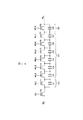
図1は、本発明の第1の実施形態に係る半導体集積回路装置の概略的な回路図を示す。図2は、本発明の第1の実施形態に係るメモリセルの断面図を示す。図3は、本発明の第1の実施形態に係るリファレンス電位選択回路の構成を示す。ここでは、上述した「TC並列ユニット直列接続型強誘電体メモリ」の1ブロック分を例にあげて説明する。 FIG. 1 is a schematic circuit diagram of a semiconductor integrated circuit device according to the first embodiment of the present invention. FIG. 2 is a sectional view of the memory cell according to the first embodiment of the present invention. FIG. 3 shows a configuration of the reference potential selection circuit according to the first embodiment of the present invention. Here, one block of the above-described “TC parallel unit serial connection type ferroelectric memory” will be described as an example.
図1に示すように、半導体集積回路装置は、TC並列ユニット直列接続型のメモリセル10と、プレート線ドライバ11と、ワード線ドライバ12と、ワード線デコーダ13と、リファレンス電位選択回路14と、第1及び第2のリファレンス電位発生回路15,16と、センスアンプ(S/A)17とを有している。
As shown in FIG. 1, the semiconductor integrated circuit device includes a TC parallel unit serial connection
TC並列ユニット直列接続型のメモリセル10は、トランジスタT1のソース/ドレインに強誘電体キャパシタC1の両端が接続され、トランジスタT2のソース/ドレインに強誘電体キャパシタC2の両端が接続され、トランジスタT3のソース/ドレインに強誘電体キャパシタC3の両端が接続され、トランジスタT4のソース/ドレインに強誘電体キャパシタC4の両端が接続されている。そして、これらの4つのセルが直列に接続され、1つのセルブロックが構成されている。このセルブロックの一端はビット線BLに接続され、セルブロックの他端はプレート線PLに接続されている。プレート線PLは、プレート線ドライバ11に接続されている。
In the TC parallel unit series connection
トランジスタT1,T2,T3,T4の各ゲートは、ワード線WL1,WL2,WL3,WL4につながっている。これらのワード線WL1,WL2,WL3,WL4にはワード線ドライバ12が接続され、このワード線ドライバ12にはワード線デコーダ13が接続されている。
The gates of the transistors T1, T2, T3, and T4 are connected to the word lines WL1, WL2, WL3, and WL4. A
ワード線デコーダ13には、リファレンス電位選択回路14が接続されている。このリファレンス電位選択回路14には、第1及び第2のレファレンス電位Vref1,Vref2を発生させるための第1及び第2のリファレンス電位発生回路15,16がそれぞれ接続されている。
A reference
センスアンプ17には、ビット線BLの出力とリファレンス電位選択回路14の出力とが入力される。そして、センスアンプ17の出力は、ビット線デコーダに接続される。
The
ここで、上記メモリセル10は、TC並列ユニット直列接続型の構造をとっているため、従来技術でも述べたように、強誘電体キャパシタの電極とビット線BLとの接続方法に関して、2種類のセルが存在する。つまり、図2に示すように、(a)上部電極がビット線BLに接続されているようなセルAと、(b)下部電極がビット線BLに接続されているようなセルBとが存在する。
Here, since the
このため、図1の回路構成では、セルA,セルBとからなる2種類の信号分布に対して、リファレンス電位Vref1,Vref2をそれぞれ発生させるためのリファレンス電位発生回路15,16が設けられている。
For this reason, in the circuit configuration of FIG. 1, reference
そして、リファレンス電位選択回路14は、図3に示すように、2つのトランジスタTref1,Tref2と、入力の反転データを出力するインバータINVとを有している。トランジスタTref1において、ソース/ドレインの一端は第1のリファレンス電位発生回路15に接続され、ソース/ドレインの他端はセンスアンプ17に接続され、ゲートはインバータINVを介してワード線デコーダ13に接続される。トランジスタTref2において、ソース/ドレインの一端は第2のリファレンス電位発生回路16に接続され、ソース/ドレインの他端はセンスアンプ17に接続され、ゲートはワード線デコーダ13に接続される。
As shown in FIG. 3, the reference
このようなリファレンス電位選択回路14では、信号量の絶対値が異なる2種類のセルA,セルBは、ワード線デコーダ13の最下位ビットが“1”,“0”のどちらかで分類できるため、このワード線デコーダ13の最下位ビットによって、Vref1とVref2のいずれかのリファレンス電位が選択されるようになっている。
In such a reference
例えば、セルAに対して、第1のリファレンス電位Vref1を設定し、セルBに対して、第2のリファレンス電位Vref2を設定する。このように設定した場合、図5に示すように、セルAとセルBとで信号分布が異なっている場合でも、セル毎にリファレンス電位を設定できるため、信号マージンを十分確保することができている。 For example, the first reference potential Vref1 is set for the cell A, and the second reference potential Vref2 is set for the cell B. In this case, as shown in FIG. 5, even if the signal distribution is different between the cell A and the cell B, the reference potential can be set for each cell, so that a sufficient signal margin can be secured. Yes.
上記第1の実施形態によれば、信号量分布が複数のグループに分かれる場合において、この分けられたグループの数だけリファレンス電位Vrefを発生させるためのリファレンス電位発生回路を設け、リファレンス電位選択回路14を用いてグループ毎にリファレンス電位Vrefを選択することができる。従って、異なる信号量分布が複数存在する場合であっても、従来技術よりも大きな余裕を持って信号マージンを確保することができる。このように、信号マージンを向上することができるため、不良ビットの問題を回避することができ、信頼性の向上や製品歩留まりの向上を図ることが可能となる。
According to the first embodiment, when the signal amount distribution is divided into a plurality of groups, the reference potential generation circuit for generating the reference potential Vref by the number of the divided groups is provided, and the reference
尚、第1の実施形態では、TC並列ユニット直列接続型強誘電体メモリを例にあげた。このTC並列ユニット直列接続型のセルでは、レイアウト上、セルの信号量が原理的に2つのグループに分けられるため、上記のような効果が大きい構造といえるが、この構造に限定されない。つまり、セルの信号量が原理的に2つ以上のグループに分けられる場合にも、第1の実施形態を適用することも可能である。この場合、グループの数だけリファレンス電位を用意し、リファレンス電位選択回路の構成も、これに合わせて複数のリファレンス電位が選択できるように変更すればよい。 In the first embodiment, the TC parallel unit serial connection type ferroelectric memory is taken as an example. In this TC parallel unit series connection type cell, the signal amount of the cell is divided into two groups in principle on the layout, so that it can be said that the above effect is great, but the structure is not limited to this. That is, the first embodiment can be applied even when the signal amount of a cell is divided into two or more groups in principle. In this case, as many reference potentials as the number of groups are prepared, and the configuration of the reference potential selection circuit may be changed so that a plurality of reference potentials can be selected in accordance with this.
[第2の実施形態]
第1の実施形態では、複数のリファレンス電位に対して、このリファレンス電位の数と同じ数のリファレンス電位発生回路を用意した。これに対して、第2の実施形態では、1つのリファレンス電位発生回路で、複数のリファレンス電位を発生させる。
[Second Embodiment]
In the first embodiment, the same number of reference potential generation circuits as the number of reference potentials are prepared for a plurality of reference potentials. In contrast, in the second embodiment, a plurality of reference potentials are generated by one reference potential generation circuit.
通常、リファレンス電位発生回路には、テスト用に複数の電位を発生させる機能をつけている場合が多い。すなわち、1つのリファレンス回路で、複数の電位を同時に発生させることも可能である。これを利用して、第2の実施形態では、第1の実施形態におけるリファレンス電位発生回路の構成を変更する。 Usually, the reference potential generation circuit often has a function of generating a plurality of potentials for testing. That is, a single reference circuit can generate a plurality of potentials simultaneously. By utilizing this, in the second embodiment, the configuration of the reference potential generation circuit in the first embodiment is changed.
図6は、本発明の第2の実施形態に係る半導体集積回路装置の概略的な回路図を示す。図7は、本発明の第2の実施形態に係るリファレンス電位選択回路の構成を示す。ここでは、第1の実施形態と同様、「TC並列ユニット直列接続型強誘電体メモリ」を例にあげて説明する。 FIG. 6 is a schematic circuit diagram of a semiconductor integrated circuit device according to the second embodiment of the present invention. FIG. 7 shows a configuration of a reference potential selection circuit according to the second embodiment of the present invention. Here, as in the first embodiment, “TC parallel unit serial connection type ferroelectric memory” will be described as an example.
図6に示すように、半導体集積回路装置は、TC並列ユニット直列接続型のメモリセル10と、プレート線ドライバ11と、ワード線ドライバ12と、ワード線デコーダ13と、リファレンス電位選択回路21と、リファレンス電位発生回路22と、センスアンプ17とを有している。
As shown in FIG. 6, the semiconductor integrated circuit device includes a TC parallel unit serial connection
ここで、図7に示すように、リファレンス電位発生回路22は、電位1から電位4の4つの電位を発生させる機能を有している。これらの電位は、例えば、電位1を最も低い電位に設定し、この電位1から順に高い電位を電位2,電位3に設定し、電位4には最も高い電位を設定する。
Here, as shown in FIG. 7, the reference
また、図7に示すように、リファレンス電位選択回路21は、電位1から電位4に対応して、トランジスタTref1,Tref2,Tref3,Tref4,Tref5,Tref6,Tref7,Tref8がそれぞれ設けられている。
As shown in FIG. 7, the reference
このような第2の実施形態では、電位1から電位4は、出力の先に接続されているトランジスタTref1,Tref2,Tref3,Tref4,Tref5,Tref6,Tref7,Tref8によって選択されて、最終的にVref1とVref2の2つの電位になっている。どのトランジスタTref1,Tref2,Tref3,Tref4,Tref5,Tref6,Tref7,Tref8を開くか、すなわちどの電位を選択するかは、例えばフューズ23の切断の情報で決定される。
In such a second embodiment, the
上記第2の実施形態によれば、第1の実施形態と同様の効果を得ることができる。さらに、第2の実施形態では、リファレンス電位発生回路22が1つでよいので、第1の実施形態に比べて、チップ面積の増大を抑制することができるという利点がある。
According to the second embodiment, the same effect as in the first embodiment can be obtained. Furthermore, in the second embodiment, since only one reference
[第3の実施形態]
第3の実施形態は、信号量分布が複数のグループに分かれる場合のグループの分け方についていくつか例示する。
[Third Embodiment]
In the third embodiment, several examples of how to divide a group when the signal amount distribution is divided into a plurality of groups will be described.
第1の例では、TC並列ユニット直列接続型のメモリセルの1ブロックにおいて、ビット線BL側の端部のセルとプレート線PL側の端部のセルと中央部のセルとよって、信号分布が異なることに着目している。 In the first example, in one block of TC parallel unit series-connected memory cells, the signal distribution is determined by the end cell on the bit line BL side, the end cell on the plate line PL side, and the center cell. Focuses on differences.
具体的には、図8に示すように、ビット線BLに最も近い端のセルを第1のグループG1とし、ビット線BLから最も遠い端のセル(プレート線PLに最も近いセル)を第2のグループG2とし、これら第1及び第2のグループG1,G2に入らない中央の7つのセルを第3のグループG3とすることで、メモリセル部10の1ブロックを3つのグループに分けている。この場合、3つのグループG1,G2,G3に分けているため、リファレンス電位は3つ用意される。
Specifically, as shown in FIG. 8, the end cell closest to the bit line BL is defined as the first group G1, and the end cell farthest from the bit line BL (cell closest to the plate line PL) is set as the second group G1. Group G2, and the seven cells in the center that are not included in the first and second groups G1 and G2 are defined as a third group G3, so that one block of the
第2の例では、TC並列ユニット直列接続型のメモリセルの1ブロックにおいて、各セルがビット線BLからどのぐらい遠いかによって、信号分布が異なることに着目している。 In the second example, attention is paid to the fact that in one block of TC parallel unit series-connected memory cells, the signal distribution differs depending on how far each cell is from the bit line BL.
具体的には、図9に示すように、ビット線BLに最も近い端のセルを第1のグループG1とし、ビット線BLから遠ざかるセルを順に第1乃至第7のグループG2,G3,G4,G5,G6,G7とし、ビット線BLから最も遠い端のセルを第8のグループG8とすることで、メモリセル部10の1ブロックを8つのグループに分けている。この場合、8つのグループG1,G2,G3,G4,G5,G6,G7,G8に分けているため、リファレンス電位は8つ用意される。
Specifically, as shown in FIG. 9, the cell at the end closest to the bit line BL is defined as the first group G1, and the cells moving away from the bit line BL are sequentially selected from the first to seventh groups G2, G3, G4. By setting G5, G6, and G7 and the cell farthest from the bit line BL as the eighth group G8, one block of the
第3の例では、メモリセル部10の平面パターンの位置によって、信号分布が異なることに着目している。
In the third example, attention is paid to the fact that the signal distribution differs depending on the position of the planar pattern of the
具体的には、図10に示すように、メモリセル部10において、中央部を第1のグループG1とし、周辺部を第2のグループG2とすることで、メモリセル部10の平面パターンを2つのグループに分けている。この場合、2つのグループG1,G2に分けているため、リファレンス電位は2つ用意される。
Specifically, as shown in FIG. 10, in the
第4の例では、チップ内のセルアレイ毎に信号分布が異なることに着目し、各セルアレイに対して1つずつリファレンス電位を設定する。各セルアレイは、レイアウト的には全く同じに作られているが、チップ内の物理的な位置が異なるため、例えば周辺回路からの距離などが微妙に異なってくる。この差異により、各セルアレイの信号量分布には微妙な差が生じるので、セルアレイ毎にグループを分けてリファレンス電位を設定することも有効である。 In the fourth example, focusing on the fact that the signal distribution is different for each cell array in the chip, one reference potential is set for each cell array. Each cell array is made exactly the same in terms of layout, but since the physical position in the chip is different, for example, the distance from the peripheral circuit is slightly different. Due to this difference, a subtle difference occurs in the signal amount distribution of each cell array. Therefore, it is also effective to set a reference potential by dividing a group for each cell array.
上記第3の実施形態によれば、第1の実施形態と同様に、各グループに対して1つずつリファレンス電位を設けることで、グループ毎の信号量分布の差異を吸収し、従来技術よりも大きな余裕を持ったリファレンス電位の設定が可能になる。 According to the third embodiment, similarly to the first embodiment, by providing one reference potential for each group, the difference in the signal amount distribution for each group is absorbed, compared to the conventional technique. The reference potential can be set with a large margin.
その他、本発明は、上記各実施形態に限定されるものではなく、実施段階ではその要旨を逸脱しない範囲で、種々に変形することが可能である。さらに、上記実施形態には種々の段階の発明が含まれており、開示される複数の構成要件における適宜な組み合わせにより種々の発明が抽出され得る。例えば、実施形態に示される全構成要件から幾つかの構成要件が削除されても、発明が解決しようとする課題の欄で述べた課題が解決でき、発明の効果の欄で述べられている効果が得られる場合には、この構成要件が削除された構成が発明として抽出され得る。 In addition, the present invention is not limited to the above-described embodiments, and various modifications can be made without departing from the scope of the invention when it is practiced. Furthermore, the above embodiments include inventions at various stages, and various inventions can be extracted by appropriately combining a plurality of disclosed constituent elements. For example, even if some constituent requirements are deleted from all the constituent requirements shown in the embodiment, the problem described in the column of the problem to be solved by the invention can be solved, and the effect described in the column of the effect of the invention Can be obtained as an invention.
10…メモリセル、11…プレート線ドライバ、12…ワード線ドライバ、13…ワード線デコーダ、14,21…リファレンス電位選択回路、15,16,22…リファレンス電位発生回路、17…センスアンプ(S/A)、23…フューズ、Tn…セルトランジスタ、Cn…強誘電体キャパシタ、BL…ビット線、PL…プレート線、WLn…ワード線、Vrefn…リファレンス電位、Trefn…リファレンス電位選択回路のトランジスタ、INV…インバータ。
DESCRIPTION OF
Claims (4)
前記セルトランジスタのゲートにそれぞれつながる複数のワード線と、
前記複数のワード線に接続されたワード線ドライバと、
前記ワード線ドライバに接続されたワード線デコーダと、
複数のリファレンス電位を発生するリファレンス電位発生回路と、
前記リファレンス電位発生回路と前記ワード線デコーダとにそれぞれ接続され、前記複数のリファレンス電位から前記グループ毎に異なるリファレンス電位を選択するリファレンス電位選択回路と、
前記リファレンス電位選択回路から出力された前記リファレンス電位が入力されるセンスアンプと
を具備し、
前記メモリセルは、強誘電体キャパシタとセルトランジスタとをそれぞれ有し、
前記セルトランジスタのソース/ドレイン間に前記強誘電体キャパシタの両端をそれぞれ接続してユニットセルを構成し、このユニットセルを複数個直列に接続したブロックであり、
前記ブロックの一端にビット線が接続され、前記ブロックの他端にプレート線が接続されていることを特徴とする半導体集積回路装置。 A plurality of memory cells each having a ferroelectric capacitor and a cell transistor and divided into a plurality of groups;
A plurality of word lines respectively connected to the gates of the cell transistors;
A word line driver connected to the plurality of word lines;
A word line decoder connected to the word line driver;
A reference potential generating circuit for generating a plurality of reference potentials;
A reference potential selection circuit connected to the reference potential generation circuit and the word line decoder, respectively, for selecting a different reference potential for each group from the plurality of reference potentials;
A sense amplifier to which the reference potential output from the reference potential selection circuit is input ;
Each of the memory cells has a ferroelectric capacitor and a cell transistor,
A unit cell is configured by connecting both ends of the ferroelectric capacitor between the source / drain of the cell transistor, and a plurality of unit cells are connected in series.
A bit line is connected to one end of the block, and a plate line is connected to the other end of the block .
前記グループ毎に異なるリファレンス電位を設定するリファレンス電位選択回路と
を具備し、
前記メモリセルは、強誘電体キャパシタとセルトランジスタとをそれぞれ有し、
前記セルトランジスタのソース/ドレイン間に前記強誘電体キャパシタの両端をそれぞれ接続してユニットセルを構成し、このユニットセルを複数個直列に接続したブロックであり、
前記ブロックの一端にビット線が接続され、前記ブロックの他端にプレート線が接続されており、
前記複数のグループは、
前記強誘電体キャパシタの上部電極が前記ビット線につながる第1のグループと、
前記強誘電体キャパシタの下部電極が前記ビット線につながる第2のグループと
を具備することを特徴とする半導体集積回路装置。 A plurality of memory cells divided into a plurality of groups;
A reference potential selection circuit for setting a different reference potential for each group;
Comprising
Each of the memory cells has a ferroelectric capacitor and a cell transistor,
A unit cell is configured by connecting both ends of the ferroelectric capacitor between the source / drain of the cell transistor, and a plurality of unit cells are connected in series.
A bit line is connected to one end of the block, and a plate line is connected to the other end of the block,
The plurality of groups are:
A first group in which an upper electrode of the ferroelectric capacitor is connected to the bit line;
A second group in which a lower electrode of the ferroelectric capacitor is connected to the bit line;
A semiconductor integrated circuit device comprising:
前記グループ毎に異なるリファレンス電位を設定するリファレンス電位選択回路と
を具備し、
前記メモリセルは、強誘電体キャパシタとセルトランジスタとをそれぞれ有し、
前記セルトランジスタのソース/ドレイン間に前記強誘電体キャパシタの両端をそれぞれ接続してユニットセルを構成し、このユニットセルを複数個直列に接続したブロックであり、
前記ブロックの一端にビット線が接続され、前記ブロックの他端にプレート線が接続されており、
前記複数のグループは、
前記ビット線側の端部に位置するセルからなる第1のグループと、
前記プレート線側の端部に位置するセルからなる第2のグループと、
前記ブロックの中央部に位置するセルからなる第3のグループと
を具備することを特徴とする半導体集積回路装置。 A plurality of memory cells divided into a plurality of groups;
A reference potential selection circuit for setting a different reference potential for each group;
Comprising
Each of the memory cells has a ferroelectric capacitor and a cell transistor,
A unit cell is configured by connecting both ends of the ferroelectric capacitor between the source / drain of the cell transistor, and a plurality of unit cells are connected in series.
A bit line is connected to one end of the block, and a plate line is connected to the other end of the block,
The plurality of groups are:
A first group of cells located at the end on the bit line side;
A second group of cells located at the end on the plate line side;
A third group of cells located in the center of the block;
A semiconductor integrated circuit device comprising:
Priority Applications (2)
| Application Number | Priority Date | Filing Date | Title |
|---|---|---|---|
| JP2003377155A JP4041054B2 (en) | 2003-11-06 | 2003-11-06 | Semiconductor integrated circuit device |
| US10/918,356 US7050338B2 (en) | 2003-11-06 | 2004-08-16 | Semiconductor integrated circuit device having memory cells divided into groups |
Applications Claiming Priority (1)
| Application Number | Priority Date | Filing Date | Title |
|---|---|---|---|
| JP2003377155A JP4041054B2 (en) | 2003-11-06 | 2003-11-06 | Semiconductor integrated circuit device |
Publications (2)
| Publication Number | Publication Date |
|---|---|
| JP2005141835A JP2005141835A (en) | 2005-06-02 |
| JP4041054B2 true JP4041054B2 (en) | 2008-01-30 |
Family
ID=34544388
Family Applications (1)
| Application Number | Title | Priority Date | Filing Date |
|---|---|---|---|
| JP2003377155A Expired - Fee Related JP4041054B2 (en) | 2003-11-06 | 2003-11-06 | Semiconductor integrated circuit device |
Country Status (2)
| Country | Link |
|---|---|
| US (1) | US7050338B2 (en) |
| JP (1) | JP4041054B2 (en) |
Families Citing this family (5)
| Publication number | Priority date | Publication date | Assignee | Title |
|---|---|---|---|---|
| US8315583B2 (en) * | 2006-08-23 | 2012-11-20 | Quellan, Inc. | Pre-configuration and control of radio frequency noise cancellation |
| JP4150326B2 (en) * | 2003-11-12 | 2008-09-17 | 株式会社リコー | Constant voltage circuit |
| US8363478B1 (en) * | 2010-02-17 | 2013-01-29 | Marvell International Ltd. | Group based read reference voltage management in flash memory |
| CN102194519B (en) * | 2010-03-08 | 2015-06-17 | 上海华虹宏力半导体制造有限公司 | Memory |
| CN102194518B (en) * | 2010-03-08 | 2016-02-24 | 上海华虹宏力半导体制造有限公司 | Storer |
Family Cites Families (8)
| Publication number | Priority date | Publication date | Assignee | Title |
|---|---|---|---|---|
| US5532953A (en) * | 1995-03-29 | 1996-07-02 | Ramtron International Corporation | Ferroelectric memory sensing method using distinct read and write voltages |
| JP3767702B2 (en) | 1995-11-16 | 2006-04-19 | ローム株式会社 | Ferroelectric memory device and memory method using ferroelectric capacitor |
| JP2000090674A (en) | 1998-09-11 | 2000-03-31 | Toshiba Corp | Semiconductor storage device and writing method and reading method thereof |
| KR100339415B1 (en) * | 1999-09-08 | 2002-05-31 | 박종섭 | Nonvolatile ferroelectric memory device |
| JP4040243B2 (en) * | 2000-09-08 | 2008-01-30 | 株式会社東芝 | Ferroelectric memory |
| JP3815982B2 (en) | 2001-06-25 | 2006-08-30 | シャープ株式会社 | Semiconductor memory device |
| JP3591497B2 (en) * | 2001-08-16 | 2004-11-17 | ソニー株式会社 | Ferroelectric nonvolatile semiconductor memory |
| US6867997B2 (en) * | 2002-03-27 | 2005-03-15 | Texas Instruments Incorporated | Series feram cell array |
-
2003
- 2003-11-06 JP JP2003377155A patent/JP4041054B2/en not_active Expired - Fee Related
-
2004
- 2004-08-16 US US10/918,356 patent/US7050338B2/en not_active Expired - Fee Related
Also Published As
| Publication number | Publication date |
|---|---|
| JP2005141835A (en) | 2005-06-02 |
| US20050099874A1 (en) | 2005-05-12 |
| US7050338B2 (en) | 2006-05-23 |
Similar Documents
| Publication | Publication Date | Title |
|---|---|---|
| JP4939528B2 (en) | Decoding circuit for non-binary group of memory line drivers | |
| JP5897337B2 (en) | Resistive memory device, layout structure thereof and sensing circuit | |
| JP2004327011A (en) | Semiconductor memory device | |
| KR20250022083A (en) | Sub-wordline driver | |
| CN102737709A (en) | Semiconductor integrated circuit device | |
| JP4050690B2 (en) | Semiconductor integrated circuit device | |
| US7126843B2 (en) | Semiconductor memory device using magnetoresistive effect | |
| JP2010262695A (en) | Semiconductor memory device | |
| JP4041054B2 (en) | Semiconductor integrated circuit device | |
| JP3265129B2 (en) | Circuit for measuring cell characteristics of nonvolatile semiconductor memory device | |
| US6094390A (en) | Semiconductor memory device with column gate and equalizer circuitry | |
| JP2000215675A (en) | Memory device and method | |
| JP2007053321A (en) | Semiconductor memory device | |
| US6834018B2 (en) | Nonvolatile memory device having data read operation with using reference cell and method thereof | |
| CN102737708A (en) | Semiconductor storage device | |
| US20080186754A1 (en) | Ferroelectric semiconductor storage device | |
| TWI798275B (en) | Dummy wordline tracking circuitry | |
| KR100817637B1 (en) | Semiconductor device and wiring method for semiconductor device | |
| JP3393600B2 (en) | Semiconductor storage device | |
| US7142447B2 (en) | Nonvolatile memory device with variable resistance element | |
| WO2023157724A1 (en) | Semiconductor memory device | |
| JP4383478B2 (en) | memory | |
| US6847536B1 (en) | Semiconductor memory device having structure for preventing level of boosting voltage applied to a node from dropping and method of forming the same | |
| US7463518B2 (en) | Layout structure for use in flash memory device | |
| US7046542B2 (en) | Semiconductor integrated circuit device |
Legal Events
| Date | Code | Title | Description |
|---|---|---|---|
| A977 | Report on retrieval |
Free format text: JAPANESE INTERMEDIATE CODE: A971007 Effective date: 20070122 |
|
| A131 | Notification of reasons for refusal |
Free format text: JAPANESE INTERMEDIATE CODE: A131 Effective date: 20070130 |
|
| A521 | Request for written amendment filed |
Free format text: JAPANESE INTERMEDIATE CODE: A523 Effective date: 20070402 |
|
| A131 | Notification of reasons for refusal |
Free format text: JAPANESE INTERMEDIATE CODE: A131 Effective date: 20070807 |
|
| A521 | Request for written amendment filed |
Free format text: JAPANESE INTERMEDIATE CODE: A523 Effective date: 20071009 |
|
| TRDD | Decision of grant or rejection written | ||
| A01 | Written decision to grant a patent or to grant a registration (utility model) |
Free format text: JAPANESE INTERMEDIATE CODE: A01 Effective date: 20071106 |
|
| A61 | First payment of annual fees (during grant procedure) |
Free format text: JAPANESE INTERMEDIATE CODE: A61 Effective date: 20071108 |
|
| FPAY | Renewal fee payment (event date is renewal date of database) |
Free format text: PAYMENT UNTIL: 20101116 Year of fee payment: 3 |
|
| FPAY | Renewal fee payment (event date is renewal date of database) |
Free format text: PAYMENT UNTIL: 20101116 Year of fee payment: 3 |
|
| FPAY | Renewal fee payment (event date is renewal date of database) |
Free format text: PAYMENT UNTIL: 20101116 Year of fee payment: 3 |
|
| FPAY | Renewal fee payment (event date is renewal date of database) |
Free format text: PAYMENT UNTIL: 20111116 Year of fee payment: 4 |
|
| FPAY | Renewal fee payment (event date is renewal date of database) |
Free format text: PAYMENT UNTIL: 20121116 Year of fee payment: 5 |
|
| FPAY | Renewal fee payment (event date is renewal date of database) |
Free format text: PAYMENT UNTIL: 20131116 Year of fee payment: 6 |
|
| LAPS | Cancellation because of no payment of annual fees |