JP4030844B2 - Digital microwave receiver - Google Patents
Digital microwave receiver Download PDFInfo
- Publication number
- JP4030844B2 JP4030844B2 JP2002269394A JP2002269394A JP4030844B2 JP 4030844 B2 JP4030844 B2 JP 4030844B2 JP 2002269394 A JP2002269394 A JP 2002269394A JP 2002269394 A JP2002269394 A JP 2002269394A JP 4030844 B2 JP4030844 B2 JP 4030844B2
- Authority
- JP
- Japan
- Prior art keywords
- pulse
- synchronization
- circuit
- signal
- packet
- Prior art date
- Legal status (The legal status is an assumption and is not a legal conclusion. Google has not performed a legal analysis and makes no representation as to the accuracy of the status listed.)
- Expired - Fee Related
Links
Images


Landscapes
- Synchronisation In Digital Transmission Systems (AREA)
- Digital Transmission Methods That Use Modulated Carrier Waves (AREA)
Description
【0001】
【発明の属する技術分野】
本発明は、デジタルマイクロ波受信機の受信信号同期回路に関し、特に放送用として映像/音声等を無線伝送するデジタルマイクロ波受信機に関する。
【0002】
【従来の技術】
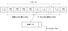
従来、放送用として映像/音声等をデジタルマイクロ波で送信する送信側では、MPEG2 TS(Transport Stream)多重化装置から送られてくるTS信号の互いに周波数の異なる複数の搬送波のそれぞれを、各搬送波に割り当てられた伝送すべき情報信号で別々に変調して、伝送フレームを構成にするためシンボル化に変換する。このようにシンボル化された伝送フレームの構成を図5に示す。
【0003】
伝送フレームは、図に示すように、周波数分割多重信号を生成した有効データとガードインターバルとからなるデータシンボルと、既知の参照信号からなる同期シンボルとから構成されて、送信側から送信される。
【0004】
一方、デジタルマイクロ波受信機では、受信した前記伝送フレームから同期シンボルを検出するため、同期シンボル内に挿入されている既知の参照信号を用意しておき、受信した前記伝送フレームの同期シンボルとの比較を行い、同期シンボル同期を生成する。同期シンボル同期の生成は、まず、受信した前記伝送フレームの同期シンボルと同期シンボル内に挿入されている既知の参照信号とを積算する。積算されたデータはシンボル単位で累算し、累算値が最大となるポイントをシンボル同期として生成する。そして、このように生成されたシンボル同期のタイミングを調整することで、復調データの制御を行っている。
【0005】
つまり、デジタル送信を行う際、デジタル伝送フレームの構成に情報データと同期用データをシンボル単位にして送信を行い、その伝送フレーム構成内に同期シンボルを挿入しているため、デジタルマイクロ波受信機ではフレーム同期の検出を容易に行うことができていた。
【0006】
【発明が解決しようとする課題】
しかし、従来の技術では、同期シンボルを挿入すると毎秒間の伝送データ内情報(有効データ)量が少なくなるため、伝送ビットレートが低下するという問題があった。
【0007】
そこで本発明はかかる問題に鑑み、同期シンボルを挿入せずに情報データのみを伝送させるため、TS信号を伝送フレーム構成に変換せずに直接デジタル変調を行って送信しても、安定した受信同期によりTS信号を出力可能とするデジタルマイクロ波受信機を提供することを目的とする。
【0008】
更に本発明は、受信信号同期回路を簡略化することによりコスト低減とハードウェア規模の縮小を可能とするデジタルマイクロ波受信機を提供することを目的とする。
【0009】
なお、デジタルマイクロ波送受信の同期検出に関して本発明に関連のある先行技術として、特開平11−32025号公報、特開平10−117189号公報、特開平10−28105公報に記載の技術が知られている。
【0010】
【課題を解決するための手段】
かかる目的を達成するために、本発明に係るデジタルマイクロ波受信機は、デジタルマイクロ波送信機にて誤り符号化されたTS信号をデジタル変調した変調波を受信するデジタルマイクロ波受信機において、復調されたTS信号から同期バイトの「B8」を検出してB8検出パルスを出力するB8検出回路と、TS信号のパケット位置を確認して同期監視を行い、TS信号、パケットの先頭位置を示すスタートパルス及び同期がはずれたことを示す同期はずれ検出パルスを出力する同期監視回路と、前記B8検出パルスの入力を基準にB8周期をカウントしてB8周期パルスを出力するB8周期カウンター回路と、前記B8検出パルスを遅延させる遅延器と、前記B8周期パルスと前記遅延器で遅延されたB8検出パルスとの位相タイミングを確認し、位相タイミングが一致するとカウンターロードパルスを出力する位相タイミング調整回路と、前記B8周期パルスの入力をカウントして、カウンターロードパルスが入力されるとカウンターをリセットすることによりB8同期を監視し、所定のカウント値になるとB8同期はずれ検出パルスを出力するB8同期監視カウンターと、前記カウンターロードパルスの入力を基準にパケット周期をカウントしてパケットの先頭位置を示すパケットスタートパルスを前記同期監視回路に出力するパケットスタートパルス生成回路と、前記B8同期はずれ検出パルス又は前記同期はずれ検出パルスのうち少なくとも一方の同期はずれ検出パルスが入力されると前記B8周期カウンター回路にリセットパルスを出力する同期はずれ検出回路とを有することとする。
【0011】
この場合、前記デジタルマイクロ波受信機は、復調したTS信号をパラレル/シリアル変換するパラシリ変換器を有し、前記B8検出回路は、前記パラシリ変換回路でパラレル/シリアル変換されたシリアルデータのTS信号を入力してシリアル/パラレル変換するシリパラ変換回路と、「B8」を定数としたB8定数パラレルデータを出力するB8定数出力回路と、前記B8定数パラレルデータと前記シリパラ変換回路で変換されたパラレルデータのTS信号を比較して同期バイトのB8を検出して前記B8検出パルスを出力するB8比較検出回路とを有することとし、更に、前記B8周期パルスを基準にして前記シリパラ変換回路で変換されたパラレルデータのTS信号の位相を調整するためのシリパラパルスを出力するシリパラ制御回路と、前記パラレルデータのTS信号を前記シリパラパルスの位相に合わせて出力する位相調整回路とを有することが望ましい。
【0012】
また、前記パケットスタートパルス生成回路は、前記カウンターロードパルスの入力を基準にパケット周期をカウントしてパケットの先頭位置を示すパケットパルスを出力するパケットカウンターと、前記パケットパルスを遅延させての位相を調整し、前記パケットスタートパルスを出力する遅延器とを有することが望ましい。
【0013】
一方、前記デジタルマイクロ波受信機は受信した受信信号の等価及び符号判定を行う符号判定機及び等価器を備えており、
前記同期はずれ検出回路から前記リセットパルスが出力されると、前記符号判定器及び等価器へリセットをかけて、再度受信信号の等価及び符号判別を行うこととする。
【0014】
【発明の実施の形態】
次に、本発明に係る実施の形態について、図面を参照して説明する。
【0015】
図1は本実施形態に係るデジタルマイクロ波受信機を示したブロック図であり、図2はデジタルマイクロ波受信機で受信するTS信号の構成を示した図である。
【0016】
まず、TS信号は先頭に1バイトの同期バイト「47(16進数)」を備えた188バイトのパケットから構成され、8パケットを1組として1フレーム構成で送受信される。この時、TS信号の信頼性向上のため、誤り訂正符号(リード・ソロモン)化される。
【0017】
この訂正符号化は、16個のパリティバイトが付加され、1パケットが204バイトに伸長される。また、パケット先頭にある同期バイトは、エネルギー拡散、インターリーブ及びRS符号化で同期をとりやすくするため、1フレーム中、8パケット毎に同期バイト「47(16進数)」を反転させて「B8(16進数)」としている。訂正符号化されたTS信号の構成を図2に示す。
【0018】
次に、本発明に係るデジタルマイクロ波受信機の構成について説明する。
【0019】
デジタルマイクロ波受信機は、作動増幅された実数部データ201及び虚数部データ202をパラレル/シリアル変換してシリアルデータ203を出力するパラシリ変換器210と、シリアルデータ203から同期バイトのB8を検出してBS検出パルス204及びTS信号232を出力するB8検出回路211と、TS信号232のパケットの位置を確認して同期監視を行い、TS信号233、スタートパルス235及び同期はずれ検出パルス234を出力する同期監視回路219と、B8検出パルス204の入力を基準にB8周期をカウントしてB8周期パルス205を出力するB8周期カウンター回路212と、B8周期パルス205と遅延器213により遅延されたB8検出パルス206の論理和をとってB8検出パルス204の位相タイミングを確認してカウンターロードパルス207を出力する論理和回路214と、B8周期パルス205の入力をカウントして、カウンターロードパルス207が入力されるとカウンターをリセットすることによりB8同期を監視し、所定のカウント値になるとB8同期はずれ検出パルス208を出力するB8同期監視カウンター216と、カウンターロードパルス207の入力を基準にパケット周期をカウントしてパケットスタートパルス231を出力するパケットスタートパルス生成回路218と、B8同期はずれ検出パルス208又は同期はずれ検出パルス234のうち少なくとも一方の同期はずれ検出パルスが入力されるとB8周期カウンター回路212にリセットパルス236を出力する論理和回路217とを備えている。
【0020】
また、B8検出回路211は更に、図3に示すように、シリアルデータ203を入力して8ビットのパラレルデータに変換するシフトレジスタ310と、TS信号の第1パケットの同期バイトである「B8」を定数としてB8定数8ビットパラレルデータを出力するB8定数314と、B8定数314からのB8定数8ビットパラレルデータと比較することにより8ビットパラレルデータ301から同期バイトのB8を検出してB8検出パルス204を出力する比較器311と、8ビットパラレルデータ301をパラレルクロックの位相に合わせるため、B8周期パルス205を基準にしてシリアルクロックを分周してシリパラパルス302を出力するシリパラ制御回路312と、8ビットパラレルデータ301をシリパラパルス302の位相に合わせてTS信号232を出力するフリップフロップ313とを備えている。
【0021】
また、パケットスタートパルス生成回路218は更に、図4に示すように、カウンターロードパルス207の入力によりカウントを開始してパケットパルス401を出力するパケットカウンター410と、パケットパルス401をTS信号232の同期バイトとの位相関係を合わせるためにタイミング調整してパケットスタートパルス231を出力する遅延器411とを備えている。
【0022】
次に、本発明に係るデジタルマイクロ波受信機の動作について説明する。
【0023】
まず、デジタル変調されたSHF帯のアナログ波信号は、デジタルマイクロ波受信機に信号が入力されると、SHFダウンコンバータによってSHFダウンコンバートされ、IFダウンコンバータ及びA/D変換器によって直交振幅復調されてIF帯からベースバンド帯に周波数変換されて実数部データと虚数部データに分離されたデジタル変調信号であるTS信号が出力される。
【0024】
この実数部データ201及び虚数部データは、それぞれパラシリ変換器210でパラレル/シリアル変換されて、TS信号の1ビットのシリアルデータ203として出力される。
【0025】
B8検出回路211はこのシリアルデータ203から同期バイトの「B8」を検出してB8検出パルス204とパラレルクロックに同期したTS信号232を出力する。
【0026】
このB8検出回路211の動作を詳細に説明すると、まずシリアルデータ203はシフトレジスタ310により8ビットパラレルデータ301として出力される。そして出力された8ビットパラレルデータ301とB8定数314から出力されるB8定数8ビットパラレルデータとを比較器311で比較し、8ビットパラレルデータ301から「B8」を検出するとB8検出パルス204を出力する。これは、図2に示すように、TS信号の構成が8パケットに1回だけ同期バイト「B8」となるため、受信同期を行うには同期バイトの「B8」検出が必要となるためである。
【0027】
TS信号内の「B8」を検出したB8検出パルス204は、B8周期カウンター回路212に入力される。
【0028】
B8周期カウンター回路212は、電源投入時、又は回線状況が悪くなって受信同期が外れた後に最初にB8検出パルス204が入力された時からカウントを開始させる。そして、「B8」周期分、つまりTS(シリアル)信号の8パケット分である8×204×8=13056分をカウントし、13056カウントが終了する度にB8周期パルス205を出力する。
【0029】
一方、B8検出パルス204は、B8周期パルス205との位相タイミング調整を行うために遅延器213により遅延され、B8検出パルス206として出力される。
【0030】
論理和回路214は、遅延器213により遅延されたB8検出パルス206と、B8周期カウンター回路212から出力されたB8周期パルス205との位相の位置確認を行い、B8検出パルス206とB8周期パルス205との位置関係が合えば、その位置は「LOW」となるカウンターロードパルス207を出力する。もし、B8検出パルス206とB8周期パルス205との位置関係が異なれば、「HIGH」のままでカウンターロードパルス207を出力する。
【0031】
このカウンターロードパルス207は、B8同期監視カウンター216及びパケットスタートパルス生成回路218に入力される。
【0032】
B8同期監視カウンター216は、カウンターロードパルス207が入力されると、これをロードパルスとしてカウンターのカウント値を初期化し、B8周期パルス205の入力により「B8」周期ごとにカウントアップする。論理和回路214においてB8検出パルス206とB8同期パルス205の位置関係が合っていれば、つまりTS信号の同期バイト「B8」の検出位置が適正であればカウンターロードパルス207は「LOW」イネーブルとなり、B8同期監視カウンター216のカウント値は初期値に戻され、再度カウントアップを始める。もし、論理和回路214においてB8検出パルス206とB8同期パルス205の位置関係が異なっていれば、つまりTS信号の同期バイト「B8」の検出位置が不適正であればカウンターロードパルス207は「HIGH」のままであるため、B8同期監視カウンター216はカウントアップして行く。
【0033】
B8同期監視カウンター216にはカウンター初期値209が設定されており、このカウンター初期値209は、所定期間内(B8周期パルス毎等)における同期バイト「B8」の許容はずれ回数を示しており、カウンターが所定期間内にカウンター初期値209以上にカウントアップすると、B8同期はずれ検出パルス208を「HIGH」として出力する。なお、カウンター初期値209は、受信システムによって特性等が異なり、本発明では0〜15まで可変設定可能としている。
【0034】
また、B8周期パルス205はB8検出回路211のシリパラ制御回路312に入力される。
【0035】
シリパラ制御回路312では、8ビットパラレルデータ301をパラレルクロックの位相に合わせるため、B8周期パルス205を基準としてシリアルクロックを分周してシリパラパルス302を出力する。フリップフロップ313は、シフトレジスタ310から出力された8ビットパラレルデータ301を、シリパラ制御回路312から出力されたシリパラパルス302でタイミング調整し、これをTS信号232として出力する。
【0036】
なお、上記回路によって同期バイト「B8」の位置が正常に検出された場合は、シフトレジスタ310から出力された8ビットパラレルデータ301はパケットの先頭からシリアル/パラレル変換されるので、より安定したTS信号232を出力することが可能となる。
【0037】
一方、論理和回路214から出力されたカウンターロードパルス207はパケットスタート生成回路218に入力される。
【0038】
パケットスタート生成回路では、パケットカウンター410はカウンターロードパルス207の入力によりカウントを開始する。TS信号の1パケット分である204カウントすると「HIGH」イネーブルをパケットパルス401として出力し、204カウント後は初期値に戻って再度204カウントを開始する。
【0039】
パケットパルス401は、B8検出回路211から出力されるTS信号232の同期バイトとの位相関係を合わせるため、遅延器411によりタイミング調整され、パケットスタートパルス231として同期監視回路219に出力される。
【0040】
同期監視回路219は、B8検出回路211から出力されるTS信号232とパケットスタートパルス231を入力とし、TS信号232の同期バイト(「B8」及び「47」)とパケットスタートパルス231との位置関係をチェックする。
【0041】
判定結果が「良」ならば、そのままの(位置関係)状態を保持し、TS信号233及びスタートパルス235を次段の誤り訂正回路に出力する。この場合、スタートパルス235とTS信号233は互いに同期しているので、誤り復号されたTS信号は安定であることが望める。しかし、判定結果が「不」ならば、B8同期監視カウンター216と同様な動作を行い、同期はずれ検出パルス234を「HIGH」として出力する。この場合、誤り復号されたTS信号233は安定であることは望めない。
【0042】
このように出力された同期はずれ検出パルス234及びB8同期はずれ検出パルス208は論理和回路217に入力され、論理和回路217は、何れかのパルスが「HIGH」となれば「HIGH」となった方のパルスをリセットパルス236として出力する。つまり、パケット周期又はB8周期の同期はずれが起こるとリセットパルス236を「HIGH」にしてB8周期カウンター回路212に入力する。
【0043】
B8周期カウンター回路212は、リセットパルス236の入力によりカウンターがリセットされ、再度B8検出パルス204の入力に基づきカウントを開始し、B8同期監視カウンター216からのB8同期はずれ検出パルス208及び同期監視カウンター219からの同期はずれ検出パルス234が共に「LOW」になるまで繰り返し行う。つまり、TS信号の同期バイトの検出位置が合うまで常時監視しているので、より安定したTS信号233を誤り訂正回路に供給することができる。
【0044】
なお、論理和回路217から「HIGH」となったリセットパルス236が出力されると、システム自体の同期が検出できていない可能性が考えられる。つまり、自局波自身が伝送されていないか、また、マルチパス等の影響による受信信号の劣化の可能性が考えられるため、論理和回路217から出力されるリセットパルス236が「HIGH」となった場合は、受信機内の符号判定器と等価器へリセットをかけて、再度受信信号の等価及び符号判別を行う。
【0045】
【発明の効果】
以上説明したように、B8同期監視カウンター及び同期監視回路において受信同期を常時監視しているため、回線状態が良好の場合は、常時安定なTS信号の出力が可能となり、回線状態が断→良好になった場合でも、受信同期を再検知するように制御し、再度安定したTS信号を出力することが可能となるため、次段の誤り訂正回路では、パケット毎に誤り訂正処理が安定に行うことができる。
【0046】
また、伝送フレーム構成を用いない本発明によれば、デジタルマイクロ波受信機における受信信号同期回路を簡略化することができるので、ハードウェア規模を大幅に縮小することができ、コスト低減にも効果がある。
【図面の簡単な説明】
【図1】本発明に係るデジタルマイクロ波受信機を示したブロック図。
【図2】TS信号の構成図。
【図3】B8検出回路の構成を示すブロック図。
【図4】パケットスタートパルス生成回路の構成を示すブロック図。
【図5】同期シンボル挿入フレームの構成図。
【符号の説明】
201 実数部データ
202 虚数部データ
203 シリアルデータ
204 B8検出パルス
205 B8周期パルス
206 B8検出パルス
207 カウンターロードパルス
208 B8同期はずれ検出パルス
209 カウンター初期値
210 パラシリ変換器
211 B8検出回路
212 B8周期カウンター回路
213 遅延器
214 論理和回路
216 B8同期監視カウンター
217 論理和回路
218 パケットスタートパルス生成回路
232 TS信号
233 TS信号
234 同期はずれ検出パルス
235 スタートパルス
236 リセットパルス
310 シフトレジスタ
311 比較器
312 シリパラ制御回路
313 フリップフロップ
314 B8定数
401 パケットパルス
410 パケットカウンター
411 遅延器[0001]
BACKGROUND OF THE INVENTION
The present invention relates to a received signal synchronizing circuit of a digital microwave receiver, and more particularly to a digital microwave receiver for wirelessly transmitting video / audio for broadcasting.
[0002]
[Prior art]
2. Description of the Related Art Conventionally, on the transmission side for transmitting video / audio and the like for broadcasting using digital microwaves, a plurality of carrier waves having different frequencies from each other in a TS signal sent from an MPEG2 TS (Transport Stream) multiplexer are used. Are separately modulated with information signals to be transmitted, and are converted into symbols to form a transmission frame. The configuration of the transmission frame symbolized in this way is shown in FIG.
[0003]
As shown in the figure, the transmission frame is composed of data symbols made up of effective data and guard intervals that generate frequency division multiplexed signals, and synchronization symbols made up of known reference signals, and is transmitted from the transmission side.
[0004]
On the other hand, in the digital microwave receiver, in order to detect a synchronization symbol from the received transmission frame, a known reference signal inserted in the synchronization symbol is prepared, and the synchronization symbol of the received transmission frame is detected. A comparison is made to generate synchronization symbol synchronization. To generate synchronization symbol synchronization, first, the synchronization symbol of the received transmission frame and the known reference signal inserted in the synchronization symbol are integrated. The accumulated data is accumulated in symbol units, and a point where the accumulated value is maximum is generated as symbol synchronization. The demodulated data is controlled by adjusting the timing of symbol synchronization generated in this way.
[0005]
In other words, when digital transmission is performed, information data and synchronization data are transmitted in symbol units in the configuration of the digital transmission frame, and a synchronization symbol is inserted in the transmission frame configuration. It was possible to easily detect frame synchronization.
[0006]
[Problems to be solved by the invention]
However, the conventional technique has a problem that the transmission bit rate is lowered because the amount of information (effective data) in transmission data per second is reduced when a synchronization symbol is inserted.
[0007]
Therefore, in view of such a problem, the present invention transmits only information data without inserting a synchronization symbol. Therefore, even if a TS signal is directly converted and transmitted without being converted into a transmission frame structure, stable reception synchronization is achieved. An object of the present invention is to provide a digital microwave receiver that can output a TS signal.
[0008]
It is another object of the present invention to provide a digital microwave receiver that can reduce the cost and hardware scale by simplifying the reception signal synchronization circuit.
[0009]
As prior art related to the present invention with respect to digital microwave transmission / reception synchronization detection, the techniques described in JP-A-11-32025, JP-A-10-117189, and JP-A-10-28105 are known. Yes.
[0010]
[Means for Solving the Problems]
In order to achieve this object, a digital microwave receiver according to the present invention is a digital microwave receiver that receives a modulated wave obtained by digitally modulating a TS signal error-coded by a digital microwave transmitter. The B8 detection circuit that detects the sync byte “B8” from the TS signal and outputs the B8 detection pulse, checks the TS signal packet position, performs synchronization monitoring, and starts the TS signal and the start position of the packet A synchronization monitoring circuit for outputting an out-of-synchronization detection pulse indicating that the pulse and the out-of-synchronization have been detected; a B8 period counter circuit for counting a B8 period based on the input of the B8 detection pulse and outputting a B8 period pulse; and the B8 A delay unit for delaying a detection pulse, and a phase timing between the B8 period pulse and the B8 detection pulse delayed by the delay unit The phase timing adjustment circuit that outputs a counter load pulse when the phase timing matches, and the B8 period pulse input is counted, and when the counter load pulse is input, the counter is reset to monitor B8 synchronization. When a predetermined count value is reached, the B8 synchronization monitoring counter that outputs a B8 synchronization loss detection pulse and the packet start pulse indicating the packet start position by counting the packet period based on the input of the counter load pulse are synchronized. When a packet start pulse generation circuit that outputs to the circuit and the B8 out-of-sync detection pulse or at least one out-of-sync detection pulse is input, the B8 cycle counter circuit outputs a reset pulse. With detection circuit And that it has.
[0011]
In this case, the digital microwave receiver has a parallel-serial converter for parallel / serial conversion of the demodulated TS signal, and the B8 detection circuit is a TS signal of serial data converted in parallel / serial by the parallel-serial conversion circuit. A serial-parallel conversion circuit that performs serial / parallel conversion, B8 constant output circuit that outputs B8 constant parallel data with “B8” as a constant, parallel data converted by the B8 constant parallel data and the serial-parallel conversion circuit And a B8 comparison and detection circuit for detecting the B8 of the synchronization byte and outputting the B8 detection pulse, and further converted by the serial-to-parallel conversion circuit based on the B8 period pulse. A serial control circuit that outputs serial pulses to adjust the phase of the TS signal of parallel data When it is desirable to have a phase adjusting circuit for outputting the combined TS signal of the parallel data to the phase of the Shiriparaparusu.
[0012]
The packet start pulse generation circuit counts a packet period based on the input of the counter load pulse and outputs a packet pulse indicating a head position of the packet, and a phase obtained by delaying the packet pulse. It is desirable to have a delay device that adjusts and outputs the packet start pulse.
[0013]
On the other hand, the digital microwave receiver is provided with a code determination device and an equalizer for performing equivalent and code determination of the received signal,
When the reset pulse is output from the out-of-synchronization detection circuit, the sign determination unit and the equalizer are reset, and the equivalent and sign determination of the received signal is performed again.
[0014]
DETAILED DESCRIPTION OF THE INVENTION
Next, embodiments according to the present invention will be described with reference to the drawings.
[0015]
FIG. 1 is a block diagram illustrating a digital microwave receiver according to the present embodiment, and FIG. 2 is a diagram illustrating a configuration of a TS signal received by the digital microwave receiver.
[0016]
First, the TS signal is composed of 188-byte packets having a synchronization byte “47 (hexadecimal number)” at the head, and is transmitted and received in one frame structure with 8 packets as one set. At this time, in order to improve the reliability of the TS signal, it is converted into an error correction code (Reed-Solomon).
[0017]
In this correction encoding, 16 parity bytes are added and one packet is expanded to 204 bytes. In addition, in order to facilitate synchronization by synchronization, interleaving, and RS coding, the synchronization byte at the head of the packet is inverted by synchronizing the synchronization byte “47 (hexadecimal number)” every 8 packets in one frame to “B8 ( Hexadecimal number) ”. FIG. 2 shows the configuration of the TS signal that has been corrected and encoded.
[0018]
Next, the configuration of the digital microwave receiver according to the present invention will be described.
[0019]
The digital microwave receiver detects a synchronization byte B8 from the
[0020]
Further, as shown in FIG. 3, the
[0021]
Further, as shown in FIG. 4, the packet start pulse generation circuit 218 further starts the count by inputting the
[0022]
Next, the operation of the digital microwave receiver according to the present invention will be described.
[0023]
First, the digitally modulated SHF band analog wave signal is SHF downconverted by the SHF downconverter when the signal is input to the digital microwave receiver, and is quadrature amplitude demodulated by the IF downconverter and A / D converter. Thus, a TS signal that is a digital modulation signal that is frequency-converted from the IF band to the baseband band and separated into real part data and imaginary part data is output.
[0024]
The real part data 201 and the imaginary part data are parallel / serial converted by the parallel-serial converter 210 and output as 1-bit
[0025]
The
[0026]
The operation of the
[0027]
The
[0028]
The B8
[0029]
On the other hand, the
[0030]
The OR
[0031]
The
[0032]
When the
[0033]
A counter initial value 209 is set in the B8
[0034]
Further, the
[0035]
The serial
[0036]
When the position of the synchronization byte “B8” is normally detected by the above circuit, the 8-bit
[0037]
On the other hand, the
[0038]
In the packet start generation circuit, the
[0039]
The
[0040]
The synchronization monitoring circuit 219 receives the TS signal 232 output from the
[0041]
If the determination result is “good”, the (positional relationship) state is maintained as it is, and the TS signal 233 and the start pulse 235 are output to the error correction circuit at the next stage. In this case, since the start pulse 235 and the TS signal 233 are synchronized with each other, it can be expected that the error-decoded TS signal is stable. However, if the determination result is “NO”, the same operation as the B8
[0042]
The out-of-synchronization detection pulse 234 and the B8 out-of-
[0043]
The B8
[0044]
Note that when the reset pulse 236 that becomes “HIGH” is output from the
[0045]
【The invention's effect】
As described above, since reception synchronization is constantly monitored by the B8 synchronization monitoring counter and the synchronization monitoring circuit, when the line state is good, it is possible to always output a stable TS signal, and the line state is broken → good. Even in such a case, it is possible to control the reception synchronization to be detected again and to output a stable TS signal again. Therefore, the error correction circuit in the next stage performs error correction processing stably for each packet. be able to.
[0046]
Further, according to the present invention that does not use a transmission frame configuration, the received signal synchronization circuit in the digital microwave receiver can be simplified, so that the hardware scale can be greatly reduced and the cost can be reduced. There is.
[Brief description of the drawings]
FIG. 1 is a block diagram showing a digital microwave receiver according to the present invention.
FIG. 2 is a configuration diagram of a TS signal.
FIG. 3 is a block diagram showing a configuration of a B8 detection circuit.
FIG. 4 is a block diagram showing a configuration of a packet start pulse generation circuit.
FIG. 5 is a configuration diagram of a synchronization symbol insertion frame.
[Explanation of symbols]
201
Claims (5)
復調されたTS信号から同期バイトの「B8」を検出してB8検出パルスを出力するB8検出回路と、TS信号のパケット位置を確認して同期監視を行い、TS信号、パケットの先頭位置を示すスタートパルス及び同期がはずれたことを示す同期はずれ検出パルスを出力する同期監視回路と、前記B8検出パルスの入力を基準にB8周期をカウントしてB8周期パルスを出力するB8周期カウンター回路と、前記B8検出パルスを遅延させる遅延器と、前記B8周期パルスと前記遅延器で遅延されたB8検出パルスとの位相タイミングを確認し、位相タイミングが一致するとカウンターロードパルスを出力する位相タイミング調整回路と、前記B8周期パルスの入力をカウントして、カウンターロードパルスが入力されるとカウンターをリセットすることによりB8同期を監視し、所定のカウント値になるとB8同期はずれ検出パルスを出力するB8同期監視カウンターと、前記カウンターロードパルスの入力を基準にパケット周期をカウントしてパケットの先頭位置を示すパケットスタートパルスを前記同期監視回路に出力するパケットスタートパルス生成回路と、前記B8同期はずれ検出パルス又は前記同期はずれ検出パルスのうち少なくとも一方の同期はずれ検出パルスが入力されると前記B8周期カウンター回路にリセットパルスを出力する同期はずれ検出回路とを有することを特徴とするデジタルマイクロ波受信機。In a digital microwave receiver that receives a modulated wave obtained by digitally modulating a TS signal error-coded by a digital microwave transmitter,
The B8 detection circuit that detects the synchronization byte “B8” from the demodulated TS signal and outputs a B8 detection pulse, and confirms the TS signal packet position to perform synchronization monitoring, and indicates the TS signal and the start position of the packet. A synchronization monitoring circuit that outputs an out-of-synchronization detection pulse indicating a start pulse and out-of-synchronization; a B8 period counter circuit that counts a B8 period based on the input of the B8 detection pulse and outputs a B8 period pulse; A delay unit that delays the B8 detection pulse, a phase timing adjustment circuit that checks a phase timing of the B8 period pulse and the B8 detection pulse delayed by the delay unit, and outputs a counter load pulse when the phase timings coincide with each other; The B8 period pulse input is counted, and when the counter load pulse is input, the counter is reset. B8 synchronization is monitored, and when a predetermined count value is reached, a B8 synchronization monitoring counter that outputs a B8 synchronization loss detection pulse, and a packet period is counted based on the input of the counter load pulse to determine the head position of the packet. A packet start pulse generation circuit that outputs a packet start pulse to the synchronization monitoring circuit, and the B8 period counter circuit when at least one of the synchronization detection pulse of the B8 synchronization detection pulse or the synchronization detection pulse is input. A digital microwave receiver comprising: an out-of-synchronization detection circuit that outputs a reset pulse.
前記同期はずれ検出回路から前記リセットパルスが出力されると、前記符号判定器及び等価器へリセットをかけて、再度受信信号の等価及び符号判別を行うことを特徴とする請求項1〜4の何れかに記載のデジタルマイクロ波受信機。The digital microwave receiver includes a code determination device and an equalizer for performing equality and code determination of the received signal received,
5. When the reset pulse is output from the out-of-synchronization detection circuit, the sign determination unit and the equalizer are reset, and the reception signal is equivalent and the code determination is performed again. A digital microwave receiver according to claim 1.
Priority Applications (1)
| Application Number | Priority Date | Filing Date | Title |
|---|---|---|---|
| JP2002269394A JP4030844B2 (en) | 2002-09-17 | 2002-09-17 | Digital microwave receiver |
Applications Claiming Priority (1)
| Application Number | Priority Date | Filing Date | Title |
|---|---|---|---|
| JP2002269394A JP4030844B2 (en) | 2002-09-17 | 2002-09-17 | Digital microwave receiver |
Publications (2)
| Publication Number | Publication Date |
|---|---|
| JP2004112125A JP2004112125A (en) | 2004-04-08 |
| JP4030844B2 true JP4030844B2 (en) | 2008-01-09 |
Family
ID=32267323
Family Applications (1)
| Application Number | Title | Priority Date | Filing Date |
|---|---|---|---|
| JP2002269394A Expired - Fee Related JP4030844B2 (en) | 2002-09-17 | 2002-09-17 | Digital microwave receiver |
Country Status (1)
| Country | Link |
|---|---|
| JP (1) | JP4030844B2 (en) |
-
2002
- 2002-09-17 JP JP2002269394A patent/JP4030844B2/en not_active Expired - Fee Related
Also Published As
| Publication number | Publication date |
|---|---|
| JP2004112125A (en) | 2004-04-08 |
Similar Documents
| Publication | Publication Date | Title |
|---|---|---|
| KR100545454B1 (en) | Digital signal system with synchronous trust counter | |
| US20080037693A1 (en) | Vehicular communications system having improved serial communication | |
| US7405650B2 (en) | Device with improved serial communication | |
| KR20000005381A (en) | Improved technique for jointly performing bit synchronization and error detection in a tdm/tdma system | |
| US20130243136A1 (en) | Method and Apparatus for Maintaining Synchronization in a Communication System | |
| US7701978B2 (en) | Method and apparatus for maintaining synchronization in a communication system | |
| US7424076B2 (en) | System and method for providing synchronization information to a receiver | |
| JP2000068972A (en) | Ofdm modulation/demodulation method and ofdm modulation/demodulation circuit | |
| JP4030844B2 (en) | Digital microwave receiver | |
| RU2121235C1 (en) | Device for formatting packetized digital data streams to transmit television information | |
| JP5359929B2 (en) | Transmission device, reception device, communication system, transmission method, and conversion method | |
| EP1478119A2 (en) | Method of recovering clock signal using user clock code in TDM digital video signal and transmitting/receiving apparatus user for the method | |
| JP3858002B2 (en) | Wireless transmission system | |
| JP2004129009A (en) | Streaming transmission device and reception device | |
| JP5069580B2 (en) | Signal reproduction device | |
| US5778010A (en) | Method and device for correcting packet data error and packet receiver | |
| JPH09149003A (en) | Method for generating frequency division multiplex signal and transmission/reception method | |
| JP3055541B2 (en) | Orthogonal frequency division multiplexed signal transmitting / receiving device | |
| JP2000068974A (en) | Ofdm receiver | |
| JP4509824B2 (en) | Diversity system receiver and received signal phase control method for diversity system receiver | |
| JP4519371B2 (en) | Transmission device, transmission device, and reception device | |
| EP1467507A2 (en) | Method and apparatus for maintaining synchronization in a communication system | |
| JP3518764B2 (en) | Orthogonal frequency division multiplex signal receiving apparatus and orthogonal frequency division multiplex signal receiving method | |
| JP3055540B2 (en) | Orthogonal frequency division multiplexed signal transmitting / receiving device | |
| JP3551096B2 (en) | Digital signal processor |
Legal Events
| Date | Code | Title | Description |
|---|---|---|---|
| RD01 | Notification of change of attorney |
Free format text: JAPANESE INTERMEDIATE CODE: A7421 Effective date: 20050330 |
|
| A621 | Written request for application examination |
Free format text: JAPANESE INTERMEDIATE CODE: A621 Effective date: 20050822 |
|
| RD01 | Notification of change of attorney |
Free format text: JAPANESE INTERMEDIATE CODE: A7421 Effective date: 20070125 |
|
| A977 | Report on retrieval |
Free format text: JAPANESE INTERMEDIATE CODE: A971007 Effective date: 20070629 |
|
| TRDD | Decision of grant or rejection written | ||
| A01 | Written decision to grant a patent or to grant a registration (utility model) |
Free format text: JAPANESE INTERMEDIATE CODE: A01 Effective date: 20071002 |
|
| A61 | First payment of annual fees (during grant procedure) |
Free format text: JAPANESE INTERMEDIATE CODE: A61 Effective date: 20071017 |
|
| R150 | Certificate of patent (=grant) or registration of utility model |
Free format text: JAPANESE INTERMEDIATE CODE: R150 |
|
| FPAY | Renewal fee payment (prs date is renewal date of database) |
Free format text: PAYMENT UNTIL: 20101026 Year of fee payment: 3 |
|
| FPAY | Renewal fee payment (prs date is renewal date of database) |
Free format text: PAYMENT UNTIL: 20101026 Year of fee payment: 3 |
|
| S531 | Written request for registration of change of domicile |
Free format text: JAPANESE INTERMEDIATE CODE: R313531 |
|
| FPAY | Renewal fee payment (prs date is renewal date of database) |
Free format text: PAYMENT UNTIL: 20101026 Year of fee payment: 3 |
|
| R350 | Written notification of registration of transfer |
Free format text: JAPANESE INTERMEDIATE CODE: R350 |
|
| LAPS | Cancellation because of no payment of annual fees |