JP3988067B2 - Electro-optical device component manufacturing method - Google Patents
Electro-optical device component manufacturing method Download PDFInfo
- Publication number
- JP3988067B2 JP3988067B2 JP37160499A JP37160499A JP3988067B2 JP 3988067 B2 JP3988067 B2 JP 3988067B2 JP 37160499 A JP37160499 A JP 37160499A JP 37160499 A JP37160499 A JP 37160499A JP 3988067 B2 JP3988067 B2 JP 3988067B2
- Authority
- JP
- Japan
- Prior art keywords
- pixel
- electro
- optical device
- liquid material
- manufacturing
- Prior art date
- Legal status (The legal status is an assumption and is not a legal conclusion. Google has not performed a legal analysis and makes no representation as to the accuracy of the status listed.)
- Expired - Fee Related
Links
Images


Landscapes
- Devices For Indicating Variable Information By Combining Individual Elements (AREA)
- Liquid Crystal (AREA)
- Ink Jet (AREA)
- Optical Filters (AREA)
Description
【0001】
【発明の属する技術分野】
本発明は、カラーフィルタ、エレクトロルミネセンス素子マトリクス等の、電気光学装置部品の製造方法に関する。特に、基板上の各画素が形成される位置にそれぞれ微小インク滴等の液状物を吐出して製造される電気光学装置部品について、乾燥速度を制御することによって、乾燥後の表面を平坦化する技術に関する。
【0002】
【従来の技術】
カラーフィルタ等の電気光学装置部品の製造方法として、インクジェット法を応用した方法が提案されている。この方法では、透明基板上に仕切りをマトリクス状に形成した後、インクジェット法を用いて液状物を仕切り内に塗布する。
【0003】
かかる従来の電気光学装置部品の製造方法においては、液状物吐出時には基板上の仕切りより上方に盛り上がる程度に液状物を付与する。これを所定温度でベークし乾燥及び硬化させると体積が減り、平坦化する。
【0004】
【発明が解決しようとする課題】
しかしながら、例えばカラーフィルタに於いて、吐出するインクのレベリング性の制御が不十分であると、乾燥時のインクの体積が大きすぎて基板上の仕切りより上方に盛り上がってしまったり、乾燥時の体積が小さすぎてへこんだ形状になってしまったりすることがある。
【0005】
図1は、インク吐出直後及び乾燥後における画素のインク面の状態を示す断面図である。図1(a)〜(c)の各図において、符号21はインク吐出直後のインク面であり、符号22はインクを乾燥及び固化させた場合のインク面である。各図に示されるように、インク吐出直後のインク面21の盛り上がりは、図1(a)〜(c)で違いがない。しかし、インクを乾燥及び固化させた場合のインク面22は、図1(a)では画素の仕切りより上側に盛り上がっており、図1(b)では画素の仕切りの上端より下方に凹んでおり、図1(c)では仕切りの上端とほぼ同じ高さで、インク面も平坦である。
【0006】
このように乾燥後のインク面に差が生じるのは、インクの量及び濃度が同一でも、乾燥条件が異なるからである。例えばインクを吐出後、高温条件下で乾燥させると、乾燥が速く進み、図1(b)のようにインクの体積が小さくなる傾向にある。逆に低温条件下で乾燥させると、乾燥が遅くなり、図1(a)のように乾燥後のインクの体積がさほど小さくならない傾向にある。
【0007】
そこで、乾燥後のインク面を図1(c)に示すような所望の状態にするには、インクの乾燥条件の制御が必要となる。しかしながら、同じカラーフィルタ基板上の画素間にもインク面のばらつきが生じることがある。特に、画素形成領域の周縁部の画素と中央部の画素との間、および、カラーフィルタ基板周縁部の画素と中央部の画素との間にばらつきが生じている。これは、画素形成領域の周縁部の乾燥速度が中央部より速く、基板周縁部の乾燥速度が基板中央部より速いことに起因すると考えられる。このような同一基板上のレベリング性の差は、色むら、色調差の原因となって好ましくない。
【0008】
この乾燥速度の違いを解決するためには、中央部の画素の乾燥を速めるためのメカニカルな工夫も考えられるが、その設計は必ずしも容易ではない。
【0009】
そこで、本発明は、簡単な構成で液状物の乾燥条件の差を抑え、色むら、色調むら、光度むらのない電気光学装置部品の製造方法を提供することを目的とする。
【0010】
上記課題を解決するために、本発明の電気光学装置部品の製造方法は、複数の画素が所定間隔をもって連続形成される画素形成領域と前記所定間隔以上にわたって画素が形成されない非形成領域とを備える基板上の当該各画素に所定の液状物を吐出することによる電気光学装置部品の製造方法であって、前記基板は、前記非形成領域によって複数の画素形成領域に区分され、前記画素形成領域の各々が複数の画素を備えて構成されており、前記画素形成領域の各画素に前記液状物を吐出する工程と、前記複数の画素形成領域の各々を取り囲む前記非形成領域の一部に、前記画素形成領域を取り囲んで前記液状物を吐出する工程と、前記吐出した液状物を乾燥させる工程と、を備え、前記非形成領域には、前記非形成領域と前記複数の画素形成領域との境界線を形成する画素に吐出する液状物の量と少なくとも同量の液状物を吐出する。
【0011】
これにより、画素領域内の液状物の乾燥条件を均一にし、乾燥後の表面を均一にすることができ、色むら、色調むら、光度むらのない電気光学装置部品を製造することができる。
【0012】
上記課題を解決するための、他の発明に係る電気光学装置部品の製造方法は、 複数の画素が所定間隔をもって連続形成される画素形成領域と前記所定間隔以上にわたって画素が形成されない非形成領域とを備える基板上の当該各画素に所定の液状物を吐出することによる電気光学装置部品の製造方法であって、前記基板は、前記非形成領域によって複数の画素形成領域に区分され、前記画素形成領域の各々が複数の画素を備えて構成されており、前記画素形成領域の各画素に前記液状物を吐出する工程と、前記複数の画素形成領域の全体を取り囲んで前記液状物を吐出する工程と、
前記吐出した液状物を乾燥させる工程と、を備える。
【0013】
また、本発明の電気光学装置部品の製造方法において、前記基板はカラーフィルタ基板であって、前記液状物としてインクを吐出するものでもよい。これにより、乾燥後のインク面を平坦にすることが容易となり、色むら、色調むらのないカラーフィルタを製造することができる。
【0017】
また、前記非形成領域内の吐出域には、基板中の最も外側の画素に吐出する液状物の量と少なくとも同量の液状物を吐出することが望ましい。
【0018】
また、本発明の電気光学装置部品の製造方法において、前記複数の画素形成領域の各々を取り囲んで前記液状物を吐出する第1の吐出域と、前記複数の画素形成領域の全体を取り囲んで前記液状物を吐出する第2の吐出域とを備えることとしてもよい。
【0019】
また、前記第2の吐出域は、前記第1の吐出域より外側に形成されることとしてもよい。
【0020】
本発明の電気光学装置部品の製造方法において、前記非形成領域内の吐出域は、前記画素形成領域との境界に沿って形成されることが好ましい。
【0021】
【発明の実施の形態】
まず、本発明の第1の実施の形態によるカラーフィルタの製造方法について、図面を参照して説明する。
【0022】
(カラーフィルタの構成)
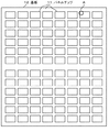
図2に、この実施形態でカラーフィルタを製造する際に用いられるカラーフィルタ基板の平面形状を示す。図3は、図2の符号Aで示す円内の拡大図である。
【0023】
図2に示されるように、カラーフィルタ基板12は、1枚のカラーフィルタとなるパネルチップ11が、平面上に複数並べられた状態となっている。この実施形態では、1枚のカラーフィルタ基板12は、8×12=96枚のパネルチップ11から構成されている。カラーフィルタの製造時には、これら複数のパネルチップ11に対してまとめてインクの吐出及び乾燥の処理を行い、その後、パネルチップ単位に切り離してカラーフィルタとする。
【0024】
図3に示されるように、パネルチップ11は、マトリクス状に並んだ画素13を備え、画素と画素の境目は、仕切り14によって区切られている。そして、複数の画素13が仕切り14を介して連続形成される画素形成領域の外側には、画素が形成されない非形成領域19がある。
【0025】
カラーフィルタの製造の際には、上記画素13の1つ1つに、赤、緑、青のいずれかのインクを数滴ずつ吐出する。図3の例では赤、緑、青の配置をいわゆるモザイク型としたが、3色が均等に配置されていれば、ストライプ型など、その他の配置でも構わない。
【0026】
図4は、図3のB−B’線断面図である。カラーフィルタ基板を構成するパネルチップ11は、透光層15と、遮光層である仕切り14とを備えている。仕切り14が形成されていない(除去された)部分は、上記画素13を形成する。この画素13に各色の液状インクを吐出し、乾燥および固化させることにより、カラーフィルタとなる。
【0027】
(吐出インクの配置)
本発明では、パネルチップのうち画素が形成されない非形成領域に、複数の画素が連続形成される画素形成領域を取り囲むようにインク滴を吐出し、画素形成領域の周縁部の乾燥条件を、画素形成領域の中央部の乾燥条件に近づけることによって、画素形成領域の周縁部の乾燥速度を適切に制御する。
【0028】
図5及び図6を用いて、本発明の実施例を具体的に説明する。図5は、本実施形態によるカラーフィルタの製造方法におけるインクの吐出パターンと、パネルチップにおける画素の配置との平面的位置関係を示したものである。図5の符号13は、各画素の位置を示す。符号17は、インクの吐出位置を示す。この図に示されるように、パネルチップ上の各画素にインクを吐出するとともに、画素が形成されない領域にも、画素形成領域との境界に沿ってインクを吐出する。特に、画素形成領域と非形成領域との境界線を形成する画素に対して、非形成領域側にもう1列の画素がある場合と同等に、いわばダミーのインク滴を吐出する第1のダミー領域を設ける。
【0029】
この場合、第1のダミー領域には、隣接する画素1つにつき、画素形成領域における1画素あたりのインク滴の量と同じかそれ以上のインク滴を、吐出することが望ましい。例えば、画素形成領域における1画素あたりのインク滴が約70ピコリットルであるとすれば、画素形成領域と非形成領域との境界線を形成する画素の隣にも、70ピコリットルまたはそれ以上のインク滴を吐出する。
【0030】
これにより、パネルチップの周縁部に位置する画素のインク乾燥条件と、パネルチップの中央部に位置する画素のインク乾燥条件を近づけることができる。画素以外の部分に吐出するインクの色は、特に限定されない。また、インクの吐出順序は特に限定されず、インクジェットヘッドの移動距離など、カラーフィルタの製造効率を考慮してプログラムすればよい。
【0031】
実際にインクを吐出して実験を行ったところ、従来の方法では、画素間の色ばらつきΔEが7であったが、本実施形態では、ΔEが3以下に収まり、ばらつきの小さいカラーフィルタを製造することができた。
【0032】
図6は、ダミー領域の配置を示す平面図である。図6に示すように、上記第1のダミー領域31の外側でかつカラーフィルタ基板12の周縁部に沿って、複数の画素形成領域の全体を取り囲むように第2のダミー領域32を設ける。この第2のダミー領域32に吐出する単位面積当たりのインク量は、カラーフィルタに吐出されるインク滴の単位面積当たりのインク量と同等にすることが望ましい。また、第2のダミー領域には、基板中の最も外側の画素に対するインク滴の量と少なくとも同量のインク滴を吐出する。これにより、カラーフィルタ基板の周縁部に位置する画素のインク乾燥条件と、カラーフィルタ基板の中央部に位置する画素のインク乾燥条件を近づけることができる。
【0033】
実際にインクを吐出して実験を行ったところ、従来の方法では、全チップ間の色ばらつきΔEが7であったが、本実施形態では、ΔEが3以下に収まり、ばらつきの小さいカラーフィルタを製造することができた。
【0034】
(カラーフィルタの製造工程)
以下、本実施形態の製造方法によるカラーフィルタの製造工程につき、更に詳細に説明する。
【0035】
膜厚0.7mm、たて38cm、横30cmの無アルカリガラスからなる透明基板の表面を、熱濃硫酸に過酸化水素水を1重量%添加した洗浄液で洗浄し、純水でリンスした後、エア乾燥を行って清浄表面を得る。この表面に、スパッタ法によりクロム膜を平均0.2μmの膜厚で形成し、金属層を得た。この金属層の表面に、フォトレジストOFPR−800(東京応化製)をスピンコートした。基板はホットプレート上で、80℃で5分間乾燥し、フォトレジスト層を形成した。
【0036】
この基板表面に、所要のマトリクスパターン形状を描画したマスクフィルムを密着させ、紫外線で露光をおこなった。次に、これを、水酸化カリウムを8重量%の割合で含むアルカリ現像液に浸漬して、未露光の部分のフォトレジストを除去し、レジスト層をパターニングした。続いて、露出した金属層を、塩酸を主成分とするエッチング液でエッチング除去した。このようにして所定のマトリクスパターンを有する遮光層(ブラックマトリクス)を得た。遮光層の膜厚は、およそ0.2μmであった。また、遮光層の幅は、およそ22μmであった。
【0037】
この基板上に、さらにネガ型の透明アクリル系の感光性樹脂組成物をやはりスピンコート法で塗布した。100℃で20分間プレベークした後、所定のマトリクスパターン形状を描画したマスクフィルムを用いて紫外線露光を行った。未露光部分の樹脂を、やはりアルカリ性の現像液で現像し、純水でリンスした後スピン乾燥した。最終乾燥としてのアフターベークを200℃で30分間行い、樹脂部を十分硬化させ、バンク層を形成した。このバンク層の膜厚は、平均で2.7μmであった。また、バンク層の幅は、およそ14μmであった。そして、遮光層は、その上面でおよそ4μmの幅のリング状露出面が形成されていた。
【0038】
得られた遮光層およびバンク層で区画された着色層形成領域のインク濡れ性を改善するため、ドライエッチング、すなわち大気圧プラズマ処理を行った。ヘリウムに酸素を20%加えた混合ガスに高電圧を印加し、プラズマ雰囲気を大気圧内でエッチングスポットに形成し、基板を、このエッチングスポット下を通過させてエッチングし、バンク層とともに着色層形成領域(ガラス基板の露出面)の活性化処理を行った。この処理の直後、対比テストプレートでの水に対する接触角は、バンク層上で平均50°であったのに対し、ガラス基板上では平均35°であった。
【0039】
この着色層形成領域に、インクジェットプリンティングヘッドから色材であるインクを高精度で制御しつつ吐出し、インクを塗布した。インクジェットプリンティングヘッドには、ピエゾ圧電効果を応用した精密ヘッドを使用し、20ピコリットルの微小インク滴を着色形成領域毎に3〜8滴、選択的に飛ばした。ヘッドよりターゲットである着色層形成領域への飛翔速度、飛行曲がり、サテライトと称される分裂迷走滴の発生防止のためには、インクの物性はもとよりヘッドのピエゾ素子を駆動する電圧と、その波形が重要である。従って、あらかじめ条件設定された波形をプログラムして、インク滴を赤、緑、青の3色を同時に塗布して所定の配色パターンの着色層を形成した。
【0040】
インクとしては、ポリウレタン樹脂オリゴマーに無機顔料を分散させた後、低沸点溶剤としてシクロヘキサノンおよび酢酸ブチルを、高沸点溶剤としてブチルカルビトールアセテートを加え、さらに非イオン系界面活性剤0.01重量%を分散剤として添加し、粘度6〜8センチポアズとしたものを用いた。
【0041】
塗布後の乾燥は、自然雰囲気中で3時間放置してインク層のセッティングを行った後、80℃のホットプレート上で40分間加熱し、最後にオーブン中で200℃で30分間加熱してインク層の硬化処理を行って、着色層を得た。この条件によって着色層、特にその透過部における膜厚のばらつきを10%以下に抑制することが出来、結果として着色層の色調の色差を3以下、さらには2以下に抑制できた。
【0042】
上記基板に、透明アクリル樹脂塗料をスピンコートして平滑面を有するオーバーコート層を得た。さらに、この上面にITOからなる電極層を所要パターンで形成して、カラーフィルタとした。得られたカラーフィルタは、熱サイクル耐久試験、紫外線照射試験、加湿試験等の耐久試験に合格し、液晶表示装置などの要素基板として十分用い得ることを確認した。
【0043】
(他の電気光学装置部品の例)
上記の実施形態は、電気光学装置部品としてカラーフィルタを例にとって説明したが、これに限らず、EL(エレクトロルミネセンス)表示装置に用いられるEL素子マトリクス、MLA(マイクロレンズアレイ)など、液状物を塗布して乾燥させる工程を備えた種々の電気光学装置部品に、本発明を適用することができる。
【0044】
【発明の効果】
本発明によれば、液状物の乾燥条件を、画素形成領域の周縁部と中央部、又は基板の周縁部と中央部で均一化することにより、色むら、色調むら、光度むらのない電気光学装置部品の製造方法を提供することができる。
【図面の簡単な説明】
【図1】インク吐出直後及び乾燥後における画素のインク面の状態を示す断面図である。
【図2】本発明の実施形態でカラーフィルタを製造する際に用いられるカラーフィルタ基板の平面図である。
【図3】図2の符号Aで示す円内の拡大図である。
【図4】図3のB−B’線断面図である。
【図5】本実施形態によるカラーフィルタの製造方法におけるインクの吐出パターンと、パネルチップにおける画素の配置との平面的位置関係を示した図である。
【図6】ダミー領域の配置を示す平面図である。
【符号の説明】
13…画素、17…液状物、19…非形成領域、21…インク吐出直後のインク面、22…インク乾燥後のインク面、12…基板、11…パネルチップ、14…仕切り、15…透光層、31…第1のダミー領域、32…第2のダミー領域[0001]
BACKGROUND OF THE INVENTION
The present invention relates to a method of manufacturing an electro-optical device component such as a color filter or an electroluminescence element matrix. In particular, the surface after drying is flattened by controlling the drying speed of electro-optical device parts manufactured by ejecting liquid materials such as fine ink droplets at positions where pixels are formed on the substrate. Regarding technology.
[0002]
[Prior art]
As a method for manufacturing electro-optical device components such as color filters, a method using an inkjet method has been proposed. In this method, after a partition is formed on a transparent substrate in a matrix, a liquid material is applied to the partition using an inkjet method.
[0003]
In such a conventional method for manufacturing an electro-optical device component, when discharging a liquid material, the liquid material is applied to the extent that it rises above the partition on the substrate. When this is baked at a predetermined temperature and dried and cured, the volume is reduced and the surface is flattened.
[0004]
[Problems to be solved by the invention]
However, for example, in a color filter, if the leveling property of the ejected ink is insufficiently controlled, the volume of the ink at the time of drying is too large and rises above the partition on the substrate, or the volume at the time of drying. May be too small and become a dented shape.
[0005]
FIG. 1 is a cross-sectional view showing the state of the ink surface of a pixel immediately after ink ejection and after drying. In each of FIGS. 1A to 1C,
[0006]
The difference in the ink surface after drying is caused because the drying conditions are different even if the amount and concentration of the ink are the same. For example, when ink is ejected and dried under high temperature conditions, the drying proceeds faster, and the ink volume tends to become smaller as shown in FIG. Conversely, when drying is performed under a low temperature condition, the drying becomes slow, and the volume of the ink after drying tends not to be so small as shown in FIG.
[0007]
Therefore, in order to bring the dried ink surface into a desired state as shown in FIG. 1C, it is necessary to control the drying conditions of the ink. However, ink surface variations may occur between pixels on the same color filter substrate. In particular, variation occurs between the peripheral pixel and the central pixel of the pixel formation region, and between the peripheral pixel and the central pixel of the color filter substrate. This is considered to be because the drying speed of the peripheral edge of the pixel formation region is faster than that of the central part, and the drying speed of the peripheral edge of the substrate is faster than that of the central part of the substrate. Such a difference in leveling property on the same substrate is not preferable because it causes uneven color and tone difference.
[0008]
In order to solve this difference in drying speed, a mechanical device for accelerating the drying of the central pixel can be considered, but its design is not always easy.
[0009]
Accordingly, an object of the present invention is to provide a method of manufacturing an electro-optical device component that has a simple configuration and suppresses a difference in drying conditions of a liquid material, and has no uneven color, uneven color, and uneven brightness.
[0010]
In order to solve the above-described problem, an electro-optical device component manufacturing method according to the present invention includes a pixel formation region in which a plurality of pixels are continuously formed with a predetermined interval, and a non-formation region in which no pixels are formed over the predetermined interval. A method of manufacturing an electro-optical device component by discharging a predetermined liquid material to each pixel on a substrate, wherein the substrate is divided into a plurality of pixel formation regions by the non-formation region. Each of which includes a plurality of pixels, the step of discharging the liquid material to each pixel of the pixel formation region, and a part of the non-formation region surrounding each of the plurality of pixel formation regions, A step of surrounding the pixel formation region and discharging the liquid material; and a step of drying the discharged liquid material, wherein the non-formation region and the plurality of pixel formations are provided in the non-formation region Discharging at least the same amount of liquid material to the amount of liquid material to be discharged to the pixels forming the boundary line between the band.
[0011]
Thereby, the drying conditions of the liquid material in the pixel region can be made uniform, the surface after drying can be made uniform, and an electro-optical device component free from uneven color, uneven color tone, and uneven luminosity can be manufactured.
[0012]
In order to solve the above problems, a method for manufacturing an electro-optical device component according to another invention includes a pixel formation region in which a plurality of pixels are continuously formed at a predetermined interval, and a non-formation region in which no pixels are formed over the predetermined interval. A method of manufacturing an electro-optical device component by discharging a predetermined liquid material to each pixel on a substrate provided with the substrate, wherein the substrate is divided into a plurality of pixel formation regions by the non-formation region, and the pixel formation Each of the regions includes a plurality of pixels, a step of discharging the liquid material to each pixel of the pixel formation region, and a step of discharging the liquid material surrounding the plurality of pixel formation regions When,
And drying the discharged liquid material.
[0013]
In the electro-optical device component manufacturing method according to the aspect of the invention, the substrate may be a color filter substrate and eject ink as the liquid material. Thereby, it becomes easy to flatten the ink surface after drying, and a color filter free from uneven color and uneven color tone can be produced.
[0017]
Further, it is desirable to discharge at least the same amount of liquid material as the amount of liquid material discharged to the outermost pixel in the substrate into the discharge area in the non-formation region.
[0018]
In the method of manufacturing an electro-optical device component according to the aspect of the invention, a first discharge area that surrounds each of the plurality of pixel formation areas and discharges the liquid material, and surrounds the whole of the plurality of pixel formation areas. It is good also as providing the 2nd discharge area which discharges a liquid material.
[0019]
Further, the second discharge area may be formed outside the first discharge area.
[0020]
In the electro-optical device component manufacturing method according to the aspect of the invention, it is preferable that the ejection area in the non-formation area is formed along a boundary with the pixel formation area.
[0021]
DETAILED DESCRIPTION OF THE INVENTION
First, a method for manufacturing a color filter according to a first embodiment of the present invention will be described with reference to the drawings.
[0022]
(Color filter configuration)
FIG. 2 shows a planar shape of a color filter substrate used when manufacturing a color filter in this embodiment. FIG. 3 is an enlarged view in a circle indicated by a symbol A in FIG.
[0023]
As shown in FIG. 2, the
[0024]
As shown in FIG. 3, the
[0025]
In manufacturing the color filter, several drops of red, green, or blue ink are ejected to each of the
[0026]
4 is a cross-sectional view taken along the line BB ′ of FIG. The
[0027]
(Disposition of ejected ink)
In the present invention, ink droplets are ejected so as to surround a pixel formation region in which a plurality of pixels are continuously formed in a non-formation region in which no pixels are formed in the panel chip, and the drying condition of the peripheral portion of the pixel formation region is set as a pixel. By approaching the drying condition at the center of the formation region, the drying speed of the peripheral portion of the pixel formation region is appropriately controlled.
[0028]
The embodiment of the present invention will be specifically described with reference to FIGS. FIG. 5 shows a planar positional relationship between the ink ejection pattern and the arrangement of pixels on the panel chip in the color filter manufacturing method according to the present embodiment.
[0029]
In this case, it is desirable that the first dummy area is ejected with ink droplets that are equal to or more than the amount of ink droplets per pixel in the pixel formation area for each adjacent pixel. For example, if the ink droplet per pixel in the pixel formation region is about 70 picoliters, 70 picoliters or more are also placed next to the pixels forming the boundary line between the pixel formation region and the non-formation region. Ink droplets are ejected.
[0030]
Thereby, the ink drying condition of the pixel located in the peripheral part of the panel chip and the ink drying condition of the pixel located in the center part of the panel chip can be made closer. The color of the ink ejected to the part other than the pixel is not particularly limited. The order of ink ejection is not particularly limited, and may be programmed in consideration of the production efficiency of the color filter, such as the moving distance of the inkjet head.
[0031]
When an experiment was performed by actually ejecting ink, in the conventional method, the color variation ΔE between pixels was 7, but in this embodiment, ΔE is less than 3 and a color filter with small variation is manufactured. We were able to.
[0032]
FIG. 6 is a plan view showing the arrangement of dummy regions. As shown in FIG. 6, a
[0033]
When an experiment was performed by actually ejecting ink, in the conventional method, the color variation ΔE between all the chips was 7, but in this embodiment, ΔE is less than 3 and a color filter with small variation is used. Could be manufactured.
[0034]
(Color filter manufacturing process)
Hereinafter, the manufacturing process of the color filter according to the manufacturing method of the present embodiment will be described in more detail.
[0035]
The surface of a transparent substrate made of non-alkali glass having a thickness of 0.7 mm, length of 38 cm, and width of 30 cm is washed with a cleaning solution in which 1% by weight of hydrogen peroxide is added to hot concentrated sulfuric acid, and rinsed with pure water. Air dry to obtain a clean surface. A chromium film with an average thickness of 0.2 μm was formed on this surface by sputtering to obtain a metal layer. Photoresist OFPR-800 (manufactured by Tokyo Ohka Kogyo Co., Ltd.) was spin coated on the surface of this metal layer. The substrate was dried on a hot plate at 80 ° C. for 5 minutes to form a photoresist layer.
[0036]
A mask film on which a required matrix pattern shape was drawn was brought into close contact with the surface of the substrate, and exposure was performed with ultraviolet rays. Next, this was immersed in an alkaline developer containing potassium hydroxide at a ratio of 8% by weight to remove the unexposed photoresist and pattern the resist layer. Subsequently, the exposed metal layer was removed by etching with an etchant containing hydrochloric acid as a main component. In this way, a light shielding layer (black matrix) having a predetermined matrix pattern was obtained. The thickness of the light shielding layer was about 0.2 μm. The width of the light shielding layer was approximately 22 μm.
[0037]
On this substrate, a negative transparent acrylic photosensitive resin composition was further applied by spin coating. After prebaking at 100 ° C. for 20 minutes, UV exposure was performed using a mask film on which a predetermined matrix pattern shape was drawn. The unexposed resin was developed with an alkaline developer, rinsed with pure water, and spin-dried. After baking as final drying was performed at 200 ° C. for 30 minutes, the resin portion was sufficiently cured, and a bank layer was formed. The bank layer had an average film thickness of 2.7 μm. The width of the bank layer was approximately 14 μm. The light shielding layer had a ring-shaped exposed surface having a width of about 4 μm on the upper surface.
[0038]
In order to improve the ink wettability of the colored layer forming region partitioned by the obtained light shielding layer and bank layer, dry etching, that is, atmospheric pressure plasma treatment was performed. A high voltage is applied to a gas mixture of helium and oxygen at 20%, a plasma atmosphere is formed at an etching spot at atmospheric pressure, and the substrate is etched by passing under the etching spot to form a colored layer together with the bank layer. The activation process of the area | region (exposed surface of a glass substrate) was performed. Immediately after this treatment, the contact angle for water on the contrast test plate averaged 50 ° on the bank layer, whereas it averaged 35 ° on the glass substrate.
[0039]
Ink was applied to the colored layer formation region from the ink jet printing head while controlling the ink as a coloring material with high accuracy, and the ink was applied. As the ink jet printing head, a precision head using the piezoelectric effect was used, and 3 to 8 droplets of 20 picoliters were selectively ejected for each color forming region. In order to prevent the flying speed from the head to the target colored layer formation area, the flight curve, and the generation of split stray droplets called satellites, not only the physical properties of the ink but also the voltage that drives the piezo element of the head and its waveform is important. Therefore, a pre-set waveform was programmed, and ink droplets were simultaneously applied with three colors of red, green, and blue to form a colored layer having a predetermined color arrangement pattern.
[0040]
As an ink, after dispersing an inorganic pigment in a polyurethane resin oligomer, cyclohexanone and butyl acetate are added as a low boiling point solvent, butyl carbitol acetate is added as a high boiling point solvent, and 0.01% by weight of a nonionic surfactant is further added. A dispersant having a viscosity of 6 to 8 centipoise was used.
[0041]
After coating, the ink layer was set by leaving it in a natural atmosphere for 3 hours, then heated on a hot plate at 80 ° C. for 40 minutes, and finally heated in an oven at 200 ° C. for 30 minutes. The layer was cured to obtain a colored layer. Under these conditions, the variation in film thickness in the colored layer, particularly in the transmission part thereof, can be suppressed to 10% or less, and as a result, the color difference of the color tone of the colored layer can be suppressed to 3 or less, and further to 2 or less.
[0042]
A transparent acrylic resin paint was spin coated on the substrate to obtain an overcoat layer having a smooth surface. Furthermore, an electrode layer made of ITO was formed on the upper surface in a required pattern to obtain a color filter. The obtained color filter passed durability tests, such as a heat cycle durability test, an ultraviolet irradiation test, and a humidification test, and confirmed that it could be sufficiently used as an element substrate for liquid crystal display devices and the like.
[0043]
(Examples of other electro-optical device parts)
In the above-described embodiment, the color filter is described as an example of the electro-optical device component. However, the present invention is not limited to this, and a liquid material such as an EL element matrix or an MLA (microlens array) used in an EL (electroluminescence) display device is used. The present invention can be applied to various electro-optical device components that include a step of applying and drying the material.
[0044]
【The invention's effect】
According to the present invention, by uniformizing the drying condition of the liquid material at the peripheral portion and the central portion of the pixel formation region or the peripheral portion and the central portion of the substrate, the electro-optic without uneven color, uneven color tone, and uneven brightness. A method for manufacturing an apparatus component can be provided.
[Brief description of the drawings]
FIG. 1 is a cross-sectional view showing a state of an ink surface of a pixel immediately after ink ejection and after drying.
FIG. 2 is a plan view of a color filter substrate used when manufacturing a color filter in an embodiment of the present invention.
FIG. 3 is an enlarged view in a circle indicated by reference symbol A in FIG. 2;
4 is a cross-sectional view taken along line BB ′ of FIG.
FIG. 5 is a diagram showing a planar positional relationship between an ink ejection pattern and a pixel arrangement in a panel chip in the color filter manufacturing method according to the present embodiment.
FIG. 6 is a plan view showing the arrangement of dummy areas.
[Explanation of symbols]
DESCRIPTION OF
Claims (7)
前記基板は、前記非形成領域によって複数の画素形成領域に区分され、前記画素形成領域の各々が複数の画素を備えて構成されており、
前記画素形成領域の各画素に前記液状物を吐出する工程と、
前記複数の画素形成領域の各々を取り囲む前記非形成領域の一部に、前記画素形成領域を取り囲んで前記液状物を吐出する工程と、
前記吐出した液状物を乾燥させる工程と、を備え、
前記非形成領域には、前記非形成領域と前記複数の画素形成領域との境界線を形成する画素に吐出する液状物の量と少なくとも同量の液状物を吐出する、
電気光学装置部品の製造方法。An electro-optical device component by ejecting a predetermined liquid material to each pixel on a substrate including a pixel forming region in which a plurality of pixels are continuously formed at a predetermined interval and a non-forming region in which pixels are not formed over the predetermined interval. A manufacturing method of
The substrate is divided into a plurality of pixel formation regions by the non-formation region, and each of the pixel formation regions includes a plurality of pixels.
Discharging the liquid material to each pixel in the pixel formation region;
Discharging the liquid material surrounding the pixel formation region to a part of the non-formation region surrounding each of the plurality of pixel formation regions;
Drying the discharged liquid material, and
In the non-formation region, a liquid material is ejected at least in the same amount as the amount of the liquid material that is ejected to pixels that form a boundary line between the non-formation region and the plurality of pixel formation regions.
Manufacturing method of electro-optical device components.
前記基板は、前記非形成領域によって複数の画素形成領域に区分され、前記画素形成領域の各々が複数の画素を備えて構成されており、
前記画素形成領域の各画素に前記液状物を吐出する工程と、
前記複数の画素形成領域の全体を取り囲んで前記液状物を吐出する工程と、
前記吐出した液状物を乾燥させる工程と、を備える
、電気光学装置部品の製造方法。An electro-optical device component by ejecting a predetermined liquid material to each pixel on a substrate including a pixel forming region in which a plurality of pixels are continuously formed at a predetermined interval and a non-forming region in which pixels are not formed over the predetermined interval. A manufacturing method of
The substrate is divided into a plurality of pixel formation regions by the non-formation region, and each of the pixel formation regions includes a plurality of pixels.
Discharging the liquid material to each pixel in the pixel formation region;
Surrounding the entire plurality of pixel formation regions and discharging the liquid material;
And a step of drying the discharged liquid material.
前記基板はカラーフィルタ基板であって、前記液状物としてインクを吐出する、電気光学装置部品の製造方法。A method of manufacturing an electro-optical device component according to claim 1,
The method of manufacturing an electro-optical device component, wherein the substrate is a color filter substrate and ejects ink as the liquid material.
前記非形成領域内の吐出域には、基板中の最も外側の画素に吐出する液状物の量と少なくとも同量の液状物を吐出する、電気光学装置部品の製造方法。A method of manufacturing an electro-optical device component according to claim 2,
A method of manufacturing an electro-optical device component, wherein at least an amount of liquid material to be discharged to an outermost pixel in the substrate is discharged to a discharge area in the non-formation region.
前記複数の画素形成領域の各々を取り囲んで前記液状物を吐出する第1の吐出域と、
前記複数の画素形成領域の全体を取り囲んで前記液状物を吐出する第2の吐出域とを備える、電気光学装置部品の製造方法。A method of manufacturing an electro-optical device component according to claim 2 or 3,
A first discharge area surrounding each of the plurality of pixel formation areas and discharging the liquid material;
A method for manufacturing an electro-optical device component, comprising: a second discharge region that surrounds the plurality of pixel formation regions and discharges the liquid material.
前記第2の吐出域は、前記第1の吐出域より外側に形成される、電気光学装置部品の製造方法。A method of manufacturing an electro-optical device component according to claim 5,
The method of manufacturing an electro-optical device component, wherein the second discharge area is formed outside the first discharge area.
前記非形成領域内の吐出域は、前記画素形成領域との境界に沿って形成される電気光学装置部品の製造方法。An electro-optical device component manufacturing method according to any one of claims 1 to 6,
A method of manufacturing an electro-optical device component in which the ejection area in the non-formation area is formed along a boundary with the pixel formation area.
Priority Applications (1)
| Application Number | Priority Date | Filing Date | Title |
|---|---|---|---|
| JP37160499A JP3988067B2 (en) | 1999-12-27 | 1999-12-27 | Electro-optical device component manufacturing method |
Applications Claiming Priority (1)
| Application Number | Priority Date | Filing Date | Title |
|---|---|---|---|
| JP37160499A JP3988067B2 (en) | 1999-12-27 | 1999-12-27 | Electro-optical device component manufacturing method |
Publications (2)
| Publication Number | Publication Date |
|---|---|
| JP2001188117A JP2001188117A (en) | 2001-07-10 |
| JP3988067B2 true JP3988067B2 (en) | 2007-10-10 |
Family
ID=18498993
Family Applications (1)
| Application Number | Title | Priority Date | Filing Date |
|---|---|---|---|
| JP37160499A Expired - Fee Related JP3988067B2 (en) | 1999-12-27 | 1999-12-27 | Electro-optical device component manufacturing method |
Country Status (1)
| Country | Link |
|---|---|
| JP (1) | JP3988067B2 (en) |
Families Citing this family (26)
| Publication number | Priority date | Publication date | Assignee | Title |
|---|---|---|---|---|
| JP3628997B2 (en) | 2000-11-27 | 2005-03-16 | セイコーエプソン株式会社 | Method for manufacturing organic electroluminescence device |
| CN1229655C (en) | 2001-06-01 | 2005-11-30 | 精工爱普生株式会社 | Color filter layer and electro-optical device |
| JPWO2003030131A1 (en) * | 2001-08-29 | 2005-01-20 | セイコーエプソン株式会社 | Electro-optical device and electronic apparatus |
| JP3944653B2 (en) * | 2001-12-06 | 2007-07-11 | セイコーエプソン株式会社 | Electro-optical device and electronic apparatus |
| US6949883B2 (en) | 2001-12-06 | 2005-09-27 | Seiko Epson Corporation | Electro-optical device and an electronic apparatus |
| JP3627739B2 (en) * | 2001-12-11 | 2005-03-09 | セイコーエプソン株式会社 | Display device and electronic device |
| CN1245703C (en) | 2001-12-11 | 2006-03-15 | 精工爱普生株式会社 | Display device and its electronic equipment |
| JP3733947B2 (en) * | 2001-12-11 | 2006-01-11 | セイコーエプソン株式会社 | Display device and electronic device |
| CN1209662C (en) * | 2001-12-17 | 2005-07-06 | 精工爱普生株式会社 | Display device and electronic apparatus |
| JP4265210B2 (en) * | 2001-12-17 | 2009-05-20 | セイコーエプソン株式会社 | Organic EL device and electronic device |
| JP3985559B2 (en) | 2002-03-19 | 2007-10-03 | セイコーエプソン株式会社 | Discharge device, liquid crystal display device manufacturing method, organic EL device manufacturing method, electron emission device manufacturing method, PDP device manufacturing method, electrophoretic display device manufacturing method, color filter manufacturing method, organic EL manufacturing method , Spacer forming method, metal wiring forming method, lens forming method, resist forming method, and light diffuser forming method |
| JP4001066B2 (en) | 2002-07-18 | 2007-10-31 | セイコーエプソン株式会社 | Electro-optical device, wiring board, and electronic equipment |
| CN100512577C (en) * | 2002-07-18 | 2009-07-08 | 精工爱普生株式会社 | Electro-optical device and electronic apparatus |
| JP4055171B2 (en) | 2004-05-19 | 2008-03-05 | セイコーエプソン株式会社 | Color filter substrate manufacturing method, electro-optical device manufacturing method, electro-optical device, and electronic apparatus |
| JP4529581B2 (en) * | 2004-08-10 | 2010-08-25 | セイコーエプソン株式会社 | Film forming method and film forming apparatus |
| JP2005310779A (en) * | 2005-04-18 | 2005-11-04 | Seiko Epson Corp | Electro-optical device and electronic apparatus |
| JP3944652B2 (en) * | 2005-04-18 | 2007-07-11 | セイコーエプソン株式会社 | Electro-optical device and electronic apparatus |
| JP4935153B2 (en) * | 2005-06-30 | 2012-05-23 | セイコーエプソン株式会社 | Droplet ejection method |
| JP2007103349A (en) * | 2005-09-08 | 2007-04-19 | Seiko Epson Corp | Film pattern forming method, organic EL device manufacturing method, color filter substrate manufacturing method, liquid crystal display device manufacturing method |
| JP4935171B2 (en) * | 2006-04-24 | 2012-05-23 | セイコーエプソン株式会社 | Film forming method, electro-optical substrate manufacturing method, electro-optical device manufacturing method, and functional film, electro-optical substrate, electro-optical device, and electronic apparatus |
| JP4361549B2 (en) * | 2006-06-09 | 2009-11-11 | 株式会社日立製作所 | Display device |
| JP5233285B2 (en) * | 2008-01-10 | 2013-07-10 | セイコーエプソン株式会社 | Electro-optical device manufacturing method and electro-optical device |
| JP4992746B2 (en) * | 2008-02-05 | 2012-08-08 | セイコーエプソン株式会社 | Thin film formation method |
| JP5169330B2 (en) * | 2008-03-06 | 2013-03-27 | セイコーエプソン株式会社 | Thin film formation method |
| JP2015066504A (en) * | 2013-09-30 | 2015-04-13 | 株式会社村田製作所 | Forming method for electronic component printing pattern, manufacturing method for electronic component, and electronic component |
| JP6487250B2 (en) * | 2015-03-27 | 2019-03-20 | 武藤工業株式会社 | Ink saturation measurement method and determination method, and ink patch chart creation method |
-
1999
- 1999-12-27 JP JP37160499A patent/JP3988067B2/en not_active Expired - Fee Related
Also Published As
| Publication number | Publication date |
|---|---|
| JP2001188117A (en) | 2001-07-10 |
Similar Documents
| Publication | Publication Date | Title |
|---|---|---|
| JP3988067B2 (en) | Electro-optical device component manufacturing method | |
| KR100470011B1 (en) | Color filter manufacturing method | |
| JP3985545B2 (en) | Thin film forming apparatus, thin film forming method, liquid crystal device manufacturing apparatus, liquid crystal device manufacturing method, liquid crystal device, thin film structure manufacturing apparatus, thin film structure manufacturing method, thin film structure, and electronic device | |
| JP4182657B2 (en) | Inkjet recording device | |
| KR101281877B1 (en) | Color filter array panel and Fabricating method thereof | |
| WO2000037972A1 (en) | Color filter and method of manufacture thereof | |
| JP3969034B2 (en) | Manufacturing method of color filter | |
| JP4138130B2 (en) | Method for manufacturing color filter and method for manufacturing liquid crystal display device | |
| JP2003156616A (en) | Color filter, method of manufacturing the same, liquid crystal device and electronic apparatus | |
| JP4100354B2 (en) | A material coating method, a color filter manufacturing method, an electroluminescence display device manufacturing method, and a plasma display device manufacturing method. | |
| CN100379560C (en) | Discharge device, coating method, manufacturing method of color filter substrate | |
| JPH11326625A (en) | Color filter, color liquid crystal display and manufacturing method thereof | |
| JP2002372613A (en) | Method for manufacturing color filter and method for manufacturing liquid crystal display device | |
| JP4035681B2 (en) | Manufacturing method of color filter | |
| US7727577B2 (en) | Apparatus and method for fabricating a liquid crystal display panel | |
| JP2001291584A (en) | Manufacturing method of electro-optical device parts | |
| JP2000180841A (en) | Manufacture of liquid crystal display element | |
| JP4438039B2 (en) | Color filter manufacturing method and manufacturing apparatus, liquid crystal panel manufacturing method, display device manufacturing method, display device panel manufacturing method | |
| JPH08179307A (en) | Production of image display panel | |
| JP2003121631A (en) | Electro-optical device and method of manufacturing the same | |
| JP2003121630A (en) | Electro-optical device and method of manufacturing the same | |
| JP5771931B2 (en) | Color filter, liquid crystal display device using the same, and method of manufacturing color filter | |
| JP2002207113A (en) | Method for producing color filter substrate and apparatus therefor | |
| JPH10206627A (en) | Color filter and manufacturing method thereof | |
| JP2002372614A (en) | Method for manufacturing color filter and method for manufacturing liquid crystal display device |
Legal Events
| Date | Code | Title | Description |
|---|---|---|---|
| A977 | Report on retrieval |
Free format text: JAPANESE INTERMEDIATE CODE: A971007 Effective date: 20060207 |
|
| A131 | Notification of reasons for refusal |
Free format text: JAPANESE INTERMEDIATE CODE: A131 Effective date: 20070313 |
|
| A521 | Request for written amendment filed |
Free format text: JAPANESE INTERMEDIATE CODE: A523 Effective date: 20070412 |
|
| A131 | Notification of reasons for refusal |
Free format text: JAPANESE INTERMEDIATE CODE: A131 Effective date: 20070509 |
|
| A521 | Request for written amendment filed |
Free format text: JAPANESE INTERMEDIATE CODE: A523 Effective date: 20070530 |
|
| TRDD | Decision of grant or rejection written | ||
| A01 | Written decision to grant a patent or to grant a registration (utility model) |
Free format text: JAPANESE INTERMEDIATE CODE: A01 Effective date: 20070621 |
|
| A61 | First payment of annual fees (during grant procedure) |
Free format text: JAPANESE INTERMEDIATE CODE: A61 Effective date: 20070704 |
|
| FPAY | Renewal fee payment (event date is renewal date of database) |
Free format text: PAYMENT UNTIL: 20100727 Year of fee payment: 3 |
|
| R150 | Certificate of patent or registration of utility model |
Free format text: JAPANESE INTERMEDIATE CODE: R150 |
|
| FPAY | Renewal fee payment (event date is renewal date of database) |
Free format text: PAYMENT UNTIL: 20110727 Year of fee payment: 4 |
|
| LAPS | Cancellation because of no payment of annual fees |