JP3980840B2 - Vapor growth apparatus and vapor growth film forming method - Google Patents
Vapor growth apparatus and vapor growth film forming method Download PDFInfo
- Publication number
- JP3980840B2 JP3980840B2 JP2001128068A JP2001128068A JP3980840B2 JP 3980840 B2 JP3980840 B2 JP 3980840B2 JP 2001128068 A JP2001128068 A JP 2001128068A JP 2001128068 A JP2001128068 A JP 2001128068A JP 3980840 B2 JP3980840 B2 JP 3980840B2
- Authority
- JP
- Japan
- Prior art keywords
- gas
- introduction pipe
- phase growth
- vapor phase
- combination
- Prior art date
- Legal status (The legal status is an assumption and is not a legal conclusion. Google has not performed a legal analysis and makes no representation as to the accuracy of the status listed.)
- Expired - Lifetime
Links
Images


Classifications
-
- C—CHEMISTRY; METALLURGY
- C23—COATING METALLIC MATERIAL; COATING MATERIAL WITH METALLIC MATERIAL; CHEMICAL SURFACE TREATMENT; DIFFUSION TREATMENT OF METALLIC MATERIAL; COATING BY VACUUM EVAPORATION, BY SPUTTERING, BY ION IMPLANTATION OR BY CHEMICAL VAPOUR DEPOSITION, IN GENERAL; INHIBITING CORROSION OF METALLIC MATERIAL OR INCRUSTATION IN GENERAL
- C23C—COATING METALLIC MATERIAL; COATING MATERIAL WITH METALLIC MATERIAL; SURFACE TREATMENT OF METALLIC MATERIAL BY DIFFUSION INTO THE SURFACE, BY CHEMICAL CONVERSION OR SUBSTITUTION; COATING BY VACUUM EVAPORATION, BY SPUTTERING, BY ION IMPLANTATION OR BY CHEMICAL VAPOUR DEPOSITION, IN GENERAL
- C23C16/00—Chemical coating by decomposition of gaseous compounds, without leaving reaction products of surface material in the coating, i.e. chemical vapour deposition [CVD] processes
- C23C16/44—Chemical coating by decomposition of gaseous compounds, without leaving reaction products of surface material in the coating, i.e. chemical vapour deposition [CVD] processes characterised by the method of coating
- C23C16/455—Chemical coating by decomposition of gaseous compounds, without leaving reaction products of surface material in the coating, i.e. chemical vapour deposition [CVD] processes characterised by the method of coating characterised by the method used for introducing gases into reaction chamber or for modifying gas flows in reaction chamber
- C23C16/45563—Gas nozzles
- C23C16/45578—Elongated nozzles, tubes with holes
-
- C—CHEMISTRY; METALLURGY
- C23—COATING METALLIC MATERIAL; COATING MATERIAL WITH METALLIC MATERIAL; CHEMICAL SURFACE TREATMENT; DIFFUSION TREATMENT OF METALLIC MATERIAL; COATING BY VACUUM EVAPORATION, BY SPUTTERING, BY ION IMPLANTATION OR BY CHEMICAL VAPOUR DEPOSITION, IN GENERAL; INHIBITING CORROSION OF METALLIC MATERIAL OR INCRUSTATION IN GENERAL
- C23C—COATING METALLIC MATERIAL; COATING MATERIAL WITH METALLIC MATERIAL; SURFACE TREATMENT OF METALLIC MATERIAL BY DIFFUSION INTO THE SURFACE, BY CHEMICAL CONVERSION OR SUBSTITUTION; COATING BY VACUUM EVAPORATION, BY SPUTTERING, BY ION IMPLANTATION OR BY CHEMICAL VAPOUR DEPOSITION, IN GENERAL
- C23C16/00—Chemical coating by decomposition of gaseous compounds, without leaving reaction products of surface material in the coating, i.e. chemical vapour deposition [CVD] processes
- C23C16/44—Chemical coating by decomposition of gaseous compounds, without leaving reaction products of surface material in the coating, i.e. chemical vapour deposition [CVD] processes characterised by the method of coating
- C23C16/458—Chemical coating by decomposition of gaseous compounds, without leaving reaction products of surface material in the coating, i.e. chemical vapour deposition [CVD] processes characterised by the method of coating characterised by the method used for supporting substrates in the reaction chamber
- C23C16/4582—Rigid and flat substrates, e.g. plates or discs
- C23C16/4583—Rigid and flat substrates, e.g. plates or discs the substrate being supported substantially horizontally
-
- C—CHEMISTRY; METALLURGY
- C30—CRYSTAL GROWTH
- C30B—SINGLE-CRYSTAL GROWTH; UNIDIRECTIONAL SOLIDIFICATION OF EUTECTIC MATERIAL OR UNIDIRECTIONAL DEMIXING OF EUTECTOID MATERIAL; REFINING BY ZONE-MELTING OF MATERIAL; PRODUCTION OF A HOMOGENEOUS POLYCRYSTALLINE MATERIAL WITH DEFINED STRUCTURE; SINGLE CRYSTALS OR HOMOGENEOUS POLYCRYSTALLINE MATERIAL WITH DEFINED STRUCTURE; AFTER-TREATMENT OF SINGLE CRYSTALS OR A HOMOGENEOUS POLYCRYSTALLINE MATERIAL WITH DEFINED STRUCTURE; APPARATUS THEREFOR
- C30B35/00—Apparatus not otherwise provided for, specially adapted for the growth, production or after-treatment of single crystals or of a homogeneous polycrystalline material with defined structure
Landscapes
- Chemical & Material Sciences (AREA)
- Engineering & Computer Science (AREA)
- Materials Engineering (AREA)
- Metallurgy (AREA)
- Organic Chemistry (AREA)
- General Chemical & Material Sciences (AREA)
- Chemical Kinetics & Catalysis (AREA)
- Mechanical Engineering (AREA)
- Crystallography & Structural Chemistry (AREA)
- Chemical Vapour Deposition (AREA)
Description
【0001】
【発明の属する技術分野】
本発明は、例えば、半導体ウエハなどの平板状または面状の基板の表面に、複数の原料ガスを用いて気相成長膜を形成するための気相成長装置および気相成長膜形成方法に関する。
【0002】
【従来の技術】
半導体装置の製造においては、例えば半導体ウエハなどよりなる基板に対して種々の処理が行われるが、例えばCVDなどの気相成長膜形成方法においては、複数の原料ガスが用いられる場合がある。
特に、例えばストロンチウム(Sr)およびチタン(Ti)を含有する有機金属含有ガスと酸素(O2)ガスとを用いるCVDによれば、シリコンウエハの表面にSrTiO3 よりなる気相成長膜を形成することができ、この気相成長膜は、その特性から、例えばキャパシタ容量絶縁膜などとして有用である。
【0003】
一般に、複数の原料ガスによる気相成長膜の形成は、通常、内部に複数のガス導入管を配設してなる反応容器を用い、この反応容器内にウエハを配置した状態で、ガス導入管の各々より原料ガスを噴出させながら加熱することにより、行われている。
【0004】
そして、従来の気相成長装置においては、ガス導入管として、通常、直管状の石英製管体の周壁に、円形貫通孔によるガス噴出口が形成されたものが広く用いられており、また、管体の周方向に伸びるスリット状貫通孔によるガス噴出口が形成されたものも知られている。
【0005】
【発明が解決しようとする課題】
しかしながら、従来の気相成長装置においては、原料ガスとして有機金属含有ガスを用いる場合には、ガス導入管におけるガス噴出口の正面方向が、原料ガスがウエハの表面に沿って当該ウエハの中心に向かう方向に噴出されるよう、当該中心方向に設定されているにもかかわらず、実際には、当該ウエハの表面に形成される気相成長膜が面方向において不均一性が相当に大きいものとなり、結局、高い均一性で所期の特性の気相成長膜を形成することができない、という問題点がある。
例えば、ストロンチウム(Sr)やチタン(Ti)を含有する有機金属含有ガスと酸素ガスとを用いる場合には、基板の面内において高い均一性で所期の結晶成長を生じさせることができないために、目的とする気相成長膜を形成することができない。
【0006】
以上の問題点について研究を重ねた結果、その原因は、ウエハの面内における有機金属含有ガスの分布における不均一性がきわめて大きいからであることが判明した。
具体的には、有機金属含有ガスは密度の高いガスであるため、ガス導入管のガス噴出口が円形口である場合には、形成される気相成長膜において、当該ガス噴出口の正面方向(ウエハの直径Rの方向とする。)では、狭い領域に或る程度の均一性が得られる場合であっても、当該直径Rから直角に離間する横方向では、離間距離が大きくなるに従って膜厚が大幅に減少するようになり、不均一性が大きい状態となることが判明した。
【0007】
そこで、ガス噴出口がウエハの面方向に伸びるスリット状貫通孔により形成されたガス導入管を用いたところ、形成される気相成長膜は、当該ガス噴出口よりの距離が小さい範囲では、ガスが横方向に拡がるために、直径Rに直角な横方向では膜厚の均一性が或る程度改善されたが、一方、直径Rの正面方向においては、ガス噴出口からの距離が大きくなるに従って膜厚が減少する程度が甚だしく、結局、不均一性が大きい状態となることが判明した。
【0008】
本発明は、以上のような知見に基づいてなされものであって、その目的は、ウエハなどの平板状の基板の表面に、有機金属含有ガスを含む複数の原料ガスによる気相成長膜を高い均一性で形成することのできる気相成長装置を提供することにある。
本発明の他の目的は、平板状の基板の表面に、有機金属含有ガスを含む複数の原料ガスによる気相成長膜を高い均一性で形成することのできる気相成長膜形成方法を提供することにある。
【0009】
【課題を解決するための手段】
本発明の気相成長装置は、平板状の基板が配置される反応容器内に、有機金属含有ガスよりなる第1のガスを供給するための第1のガス導入管と、当該有機金属含有ガスと反応し、当該有機金属含有ガスより密度の小さい第2のガスを供給するための第2のガス導入管とが配設されてなり、
第1のガス導入管において、ガス噴出口が、基板の面に沿って伸びるスリット状貫通孔により形成されており、第2のガス導入管のガス噴出口が、円形貫通孔により形成されており、
第1のガス導入管のガス噴出口と、第2のガス導入管のガス噴出口とは、反応容器内の基板の外周方向に沿って並んで配置され、
第1のガス導入管のガス噴出口よりの第1のガスが、第2のガス導入管のガス噴出口よりの第2のガスの流れにより、基板の面に沿って延展拡散されることを特徴とする。
【0010】
以上の第1のガス導入管のガス噴出口を形成するスリット状貫通孔は、その開き角が30〜160度であることが好ましい。
第1のガス導入管のガス噴出口は、当該第1のガス導入管の周方向に並ぶ複数のスリット孔部分により形成されていてもよい。
【0011】
以上において、第1のガス導入管のガス噴出口および第2のガス導入管のガス噴出口は、各々の正面方向が、基板の中心における角度45度の範囲内にあることが好ましい。
【0012】
本発明の気相成長膜形成方法は、上記の気相成長装置を用いて、平板状の基板の表面に気相成長膜を形成することを特徴とする。
【0013】
本発明において、第1のガスおよび第2のガスが、下記の組合せから選ばれたものとすることができる。
(1)Sr〔[(CH3)3 CCO]2CH〕2 ガスとO2 ガスとの組合せ
(2)Ti (OC3 H7 −i)2〔[(CH3)3 CCO]2CH〕2 ガスとO2 ガスとの組合せ
(3)TiCl4ガスとNH3 ガスとの組合せ
(4)Zr〔OC(CH3)3 〕4 ガスとO2 ガスとの組合せ
(5)Ta(OC2 H5)5 ガスとO2 ガスとの組合せ
【0014】
【作用】
本発明の気相成長装置によれば、原料ガスの一部として密度の高い有機金属含有ガスを用いる場合であっても、当該有機金属含有ガスよりなる第1のガスが、密度の低い第2のガスのガス噴出口と基板の外周方向に並んで配置されているガス噴出口から噴出されるため、当該第1のガスは、第2のガスの流れによって基板の面に沿って延展拡散されることとなり、その結果、当該有機金属含有ガスをウエハの表面に十分に高い均一性で供給することができ、従って、当該基板の表面に、その全体にわたって、高い均一性で所望の気相成長膜を形成することができる。
【0015】
【発明の実施の形態】
以下、図面を参照して、本発明について詳細に説明する。
図1は、本発明の気相成長装置の構成の一例を概略的に示す説明図である。
この気相成長装置10は、バッチ式縦型気相成長装置であって、上下方向に伸びる円筒状であって上部が閉塞された、例えば石英よりなる反応容器12を備えている。
【0016】
反応容器12の下方には、円筒状のステンレス鋼からなるマニホールド13が当該反応容器12の下端に接続されている。このマニホールド13の下方には蓋体14が配置されており、この蓋体14は、ボートエレベータ(図示せず)により上下方向に移動可能とされている。
そして、蓋体14が上昇してマニホールド13の下端の開口が閉塞されることにより、反応容器12の内部に密閉された反応処理室が形成される。
【0017】
蓋体14上には、保温筒15を介して、例えば石英からなるウエハボートWBが載置される。気相成長膜を形成すべき例えばシリコンよりなる半導体ウエハWは、その複数枚が、このウエハボートWBに上下方向に所定の間隔をおいて保持される。そして、ボートエレベータによって蓋体14が上昇されてウエハボートWBが反応容器12内に挿入されることにより、当該ウエハボートWBに保持されたウエハWは、反応容器12内における処理領域に配置される。
【0018】
反応容器12は、内部にウエハボートWBが挿入された状態で、反応容器12の内側面とウエハボートWBまたはウエハWの外周縁との間に円筒状空隙が形成される大きさとされており、この円筒状空隙内に、後述するガス導入管が配設される。
【0019】
反応容器12の周囲には、例えば抵抗発熱体からなる筒状ヒータ16が設けられており、この筒状ヒータ16により、反応容器12の内部温度または配置されたウエハWの温度が所定の設定温度となるよう加熱される。
そして、筒状ヒータ16の外側には断熱材層18が配設されており、更に、マニホールド13以外の全体を包囲するアウターシェル20が設けられている。また、必要に応じて、反応容器12の上方にもヒータが配設される。
【0020】
反応容器12内に原料ガスを供給するための複数のガス供給管が設けられている。具体的には、有機金属含有ガスを供給するための第1のガス供給管30と、酸素ガスを供給するための第2のガス供給管40とが、各々、マニホールド13の周壁を互いに隣接した位置において貫通して伸びるよう設けられている。
【0021】
第1のガス供給管30は、当該気相成長装置10の外部に設けられた、有機金属含有ガスよりなる原料ガス源(図示せず)に接続されると共に、マニホールド13の内部における先端部には、反応容器12の内周面とウエハWの外周縁との間における円筒状空隙内に配置された、例えば石英管よりなる第1のガス導入管32の下端部が連通して接続されている。
【0022】
図2は、第1のガス導入管をウエハの中心から見た状態で示す説明用正面図であり、図3(イ)は、図2の第1のガス導入管の一部の拡大正面図、図3(ロ)は、図2の第1のガス導入管のガス噴出口を通る拡大横断面図である。
また、図4は、反応容器内に配置されたウエハに対する、第1のガス導入管の噴出管部分のスリット状噴出口、並びに、第2のガス導入管の噴出管部分の円形噴出口の位置関係を示す説明図である。
【0023】
図2に示されているように、第1のガス導入管32は、反応容器12内の円筒状空隙内を上方に伸びる導入管部分32Aと、この導入管部分32Aの上端からU字状に湾曲して下方に伸びる噴出管部分32Bとを有してなり、互いに並行して伸びる噴出管部分32Bと導入管部分32Aとの間には、適宜の個所において補強用ブリッジ部材33が連結されている。
【0024】
噴出管部分32Bにおいては、各々管体の周方向(すなわち、ウエハWの面方向)に伸びるスリット状貫通孔によって形成されたガス噴出口(以下、「スリット状噴出口」という。)35の多数が、当該噴出管部分32Bの長さ方向において適宜の間隔で形成されている。
そして、図4に示すように、ウエハWの面に沿って伸びる各スリット状噴出口35は、矢印Xで示すその正面方向が、ウエハWの中心Cを向いた状態とされている。なお、図4においては、導入管部分32Aは省略され、噴出管部分32Bが簡略に示されている。
【0025】
第1のガス導入管32の寸法は特に限定されるものではなく、種々の条件に応じて適宜設定することができるが、一例を示すと、第1のガス導入管32の噴出管部分32Bの外径は16.8〜17.2mm、内径は16.5〜16.6mm、肉厚は0.2〜0.7mmとされる。また、スリット状噴出口35の長さ(噴出管部分32Bの管体における周方向の長さ)は、その開き角α(図2(ロ)参照)の大きさが例えば30〜160度となる大きさとされ、また、開口幅(噴出管部分32Bの管体の長さ方向の幅)dは0.5〜2.0mmの範囲の大きさとされる。
【0026】
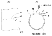
図5は、スリット状噴出口35の変形例を示し、(イ)および(ロ)は、それぞれ、図3の(イ)および(ロ)と同様の図である。この図5からも明らかなように、スリット状噴出口35の各々は、単一のスリット孔のみよりなるものである必要はなく、管体の周方向において複数(図5の例では3つ)のスリット孔部分Sに分割され、隣接するスリット孔部分S間に中間壁部分Mが残存している状態のスリット状噴出口35であってもよい。この場合には、中間壁部分Mが残存していることにより、大きな機械的強度が得られる点で、好ましい。
【0027】
第2のガス供給管40は、第1のガス供給管30と同様にマニホールド13の周壁を貫通して配設されており、当該気相成長装置10の外部に設けられた酸素ガス源(図示せず)に接続されると共に、マニホールド13の内部における先端部には、反応容器12の内周面とウエハWの外周縁との間における円筒状空隙内に配置された、例えば石英管よりなる第2のガス導入管(図1では示されていない。)の下端部が連通して接続されている。
【0028】
図6は、第2のガス導入管を示す説明図であって、(イ)はウエハの中心から見た正面図、(ロ)はガス噴出口を示す拡大正面図、(ハ)はガス噴出口を通る拡大横断面図である。
図6に示されているように、第2のガス導入管42は、円筒状空隙内を上方に伸びる導入管部分42Aと、この導入管部分42Aの上端からU字状に湾曲して下方に伸びる噴出管部分42Bとを有してなり、互いに並行して伸びる噴出管部分42Bと導入管部分42Aとの間には、適宜の個所において、補強用ブリッジ部材43が連結されている。
【0029】
噴出管部分42Bにおいては、円形貫通孔によって形成されたガス噴出口(以下、「円形噴出口」という。)45の多数が、当該噴出管部分42Bの長さ方向において適宜の間隔で形成されている。
そして、図4に示されているように、噴出管部分42Bにおける各円形噴出口45は、矢印Yで示すその正面方向が、ウエハWの中心Cを向いた状態とされている。なお、図4においては、導入管部分42Aは省略され、噴出管部分42Bが簡略に示されている。
【0030】
ここに、第2のガス導入管42の管体としては、既述の第1のガス導入管32と同様のものが用いられる。円形噴出口45の大きさは、種々の条件に応じて適宜設定することができるが、例えば直径が0.5〜5.0mmとされる。円形噴出口45は、例えば管体の周方向に並ぶ複数の円形貫通孔によって形成することもできる。
【0031】
以上において、第1のガス導入管32の噴出管部分32Bと、第2のガス導入管42の噴出管部分42Bとは、図4に示されているように、ウエハWの外周の方向に沿って接近した位置に並んで配置されており、既述のように、それらのガス噴出口すなわちスリット状噴出口35と円形噴出口45とはいずれもその正面方向がウエハWの中心Cを向いた状態に設定されている。
【0032】
そして、スリット状噴出口35と円形噴出口45とは、各々の正面方向のなす角度、すなわち矢印Xと矢印Yとのなす角度(以下「噴出口間角度」という。)θが小さい状態で並んで配置されていることが必要である。実際上、この噴出口間角度θの大きさは45度以下であることが重要であって、特に10度以下であることが好ましく、この場合には、形成される気相成長膜を均一性のきわめて高いものとすることができる。
なお、噴出口間角度θの大きさの下限は特に定める必要はないが、噴出管部分32Bおよび噴出管部分42Bを完全に同一の位置に配置することは物理的に不可能であって自ずと限度がある。
【0033】
また、マニホールド13における、第1のガス供給管30および第2のガス供給管40が貫通する位置とは反対側の位置には排気口19が設けられており、この排気口19には、調節バルブが介挿された排気管を介して真空ポンプ(図示せず)が接続されている。
【0034】
そして、上記の第1のガス供給管30および第2のガス供給管40によるガスの供給、筒状ヒータ16の動作、並びに排気口19に接続された調節バルブおよび真空ポンプの動作状態を制御するための制御機構(図示せず)が設けられている。この制御機構は、具体的には、マイクロプロセッサやプロセスコントローラなどにより構成され、予定のプログラムに基づいて制御信号を各部に供給して制御する機能を有する。
【0035】
本発明においては、例えば上記のような構成を有する気相成長装置10を用いて、以下のようにして、ウエハの表面に気相成長膜を形成する。
先ず、気相成長膜を形成するべきウエハWを保持させた状態のウエハボートWBを、降下されている蓋体14上に載置した後、図示されていないボートエレベータにより蓋体14を上昇させ、ウエハボートWBを反応容器12内に挿入することによりウエハWを反応容器12内に配置すると共に、蓋体14によりマニホールド13の下端の開口を閉塞することにより、反応容器12内を密閉された状態とする。
【0036】
一方、反応容器12内は、排気口19を介して設定された減圧状態とされると共に、筒状ヒータ16によって加熱されることにより、設定された温度状態に維持される。
この減圧状態および温度状態は、目的とする気相成長膜の種類や用いられる原料ガスの種類およびそれらの流量、その他の条件によって適宜選定される。
反応容器12内の雰囲気についての条件の一例では、圧力が例えば67〜670Pa(0.5〜5.0Torr)であり、温度は300〜600℃である。
【0037】
そして、第1のガス供給管30および第2のガス供給管40からそれぞれ所要の原料ガスが供給され、設定された減圧条件および温度条件が維持されている状態において、気相成長膜の形成が行われる。
【0038】
第1のガス供給管30および第2のガス供給管40に供給される原料ガスは、目的とする気相成長膜の種類によって異なるが、第1のガス供給管30による第1のガスとしては有機金属含有ガスが用いられる。一方、第2のガス供給管40による第2のガスとしては、当該第1のガス供給管30に供給される有機金属含有ガスと反応し、しかも当該有機金属含有ガスより密度の小さい反応用ガスが用いられる。
各原料ガスの供給割合は、経験的に目的とする状態の気相成長膜が形成される条件に従って設定することができる。
【0039】
気相成長膜を形成するために用いられる有機金属含有ガス、およびこれと共に用いられる反応用ガスの具体的な組合せとしては、下記のものを挙げることができるが、これらに限定されるものではない。
(1)Sr〔[(CH3)3 CCO]2CH〕2 ガス(以下「Sr(DPM)2 ガス」という。)とO2 ガスとの組合せ
この組合せによれば、SrOよりなる気相成長膜が形成される。
(2)Ti (OC3 H7 −i)2〔[(CH3)3 CCO]2CH〕2 ガスとO2 ガスとの組合せ
この組合せによれば、TiO2 よりなる気相成長膜が形成される。
(3)TiCl4ガスとNH3 ガスとの組合せ
この組合せによれば、TiNよりなる気相成長膜が形成される。
(4)Zr〔OC(CH3)3 〕4 ガスとO2 ガスとの組合せ
この組合せによれば、ZrO2 よりなる気相成長膜が形成される。
(5)Ta(OC2 H5)5 ガスとO2 ガスとの組合せ
この組合せによれば、Ta2 O5 よりなる気相成長膜が形成される。
以上の組合せの各々は、それが単独で用いられることは必須でない。例えば、上記(1)と(2)の組合せを併用して、Sr(DPM)2 ガスおよびTi (OC3 H7 −i)2〔[(CH3)3 CCO]2CH〕2 ガスの混合ガスと、酸素ガスとの組合せを用いることにより、SrTiO3 よりなる気相成長膜を形成することができる。
【0040】
例えば、上記(1)の組合せのガスによって気相成長膜を形成する場合には、第1のガス供給管30には、Sr(DPM)2 ガスを例えば0.3〜1.0slmの割合で供給すると共に、第2のガス供給管40には酸素ガスを例えば1.0〜10.0slmの割合で供給し、反応容器12内は、67〜670Pa(0.5〜5.0Torr)の減圧状態および300〜600℃の温度状態に維持される。
成膜に要する時間は、目的とする膜厚の大きさによっても異なるが、例えば、10〜40分間とされ、これにより、膜厚が例えば5〜20nmの気相成長膜が形成される。
【0041】
以上の気相成長膜の形成においては、第1のガス供給管30より供給された有機金属含有ガスは、反応容器12内の第1のガス導入管32を介して噴出管部分32Bに至り、この噴出管部分32Bに形成されたスリット状噴出口35の各々から、ウエハWの面に沿ってその中心Cに向かって噴出される。
これと同時に、第2のガス供給管40より供給された酸素ガスは、反応容器12内の第2のガス導入管42を介して噴出管部分42Bに至り、この噴出管部分42Bに形成された円形噴出口45の各々から、ウエハWの面に沿ってその中心Cに向かって噴出される。
【0042】
噴出管部分32Bより噴出される有機金属含有ガスは、スリット状噴出口35が、ウエハWの面に沿って水平方向に伸びるスリット状貫通孔により形成されているため、噴出された後にウエハWの面に沿って、矢印方向Xの正面方向と直角な方向(横方向)にも大きく拡散するようになる。
しかし、この有機金属含有ガスは、その組成において金属元素を含有するために密度が高くて重いものであり、従って、当該スリット状噴出口35からX方向において遠くにまで拡散することが困難であり、そのために、従来においてはX方向における膜厚の不均一性が大きくなることを抑制することがほとんど不可能であった。
【0043】
然るに、噴出管部分32Bよりの有機金属含有ガスの噴出と同時に、第2のガス導入管42に連続する噴出管部分42Bの円形噴出口45からは、酸素ガスが噴出される。この酸素ガスは、その密度の低くて軽いものであるために、それ自体が噴出口の形状によらずに、従って当該噴出口が円形であってもウエハWの表面に沿って大きく拡がって高い均一性で拡散するようになる。
【0044】
然るに、この酸素ガスの噴出口である円形噴出口45は、有機金属含有ガスを噴出させる噴出管部分32Bのスリット状噴出口35と、ウエハWの外周方向に沿って互いに接近して並んで配置されているため、スリット状噴出口35からの有機金属含有ガスは、酸素ガスの流れの作用を受け、酸素ガスの拡散作用によって延展拡散されることとなり、その結果、X方向においても、大きな距離の範囲において高い均一性を得ることができる。
以上の結果、ウエハWの表面においては、有機金属含有ガスおよび酸素ガスが両方共に高い均一性で拡散することとなり、従って、その膜厚においても、また膜質においても、高い均一性の気相成長膜を形成することができる。
【0045】
以上の気相成長装置10においては、ガス導入管(第1のガス導入管32および第2のガス導入管42)が、いずれも、反応容器12内において、上方に伸びる導入管部分(32Aおよび42A)と、この導入管部分の上端からU字状に湾曲して下方に伸びる噴出管部分(32Bおよび42B)とにより構成されたものが用いられている。これは、反応容器12がいわゆる単管構造のものであって、当該反応容器12内を減圧化するための排気が下部の排気口19により行われることから、噴出管部分(32Bおよび42B)が下方に伸びるものであることにより、その長さ方向に並んだ状態に形成された各噴出口のレベルの差による噴出圧力の差を小さくすることができ、全体として均一性の高い噴出状態を得ることができるからである。
【0046】
図7は、本発明の気相成長装置の構成の他の一例を概略的に示す説明図、図8は、この気相成長装置における第1のガス導入管および第2のガス導入管の説明図である。
この例の気相成長装置50は、基本的には、図1の気相成長装置10と同様の構成を有するが、次の点で異なっている。すなわち、この気相成長装置50は、反応容器12の内周壁に沿って上部が開放された内管52が設けられている二重管型のものであって、当該内管52と反応容器12との間に環状空間54が形成されており、この環状空間54の下部に排気口19が接続されている。
【0047】
そして、図8(イ)に示すように、第1のガス供給管30に接続された第1のガス導入管56は、単に上方に伸びる直管状の管体からなり、これにスリット状噴出口35が形成されて構成されている。また、図8(ロ)に示すように、第2のガス供給管40に接続された第2のガス導入管58も同様に、単に上方に伸びる直管状の管体からなるものとされ、これに円形噴出口45が形成されて構成されている。
【0048】
このような二重管型の構成では、反応容器12内においては、環状空間54を介して上方から反応容器12内の排気が行われるため、上記のような直管状のガス導入管56および58により、既述の例におけると同様に、長さ方向に並んだ状態に形成された各噴出口のレベルの差による噴出圧力の差を小さくすることができ、全体として均一性の高い噴出状態を得ることができる。
【0049】
以上、本発明の気相成長装置および気相成長膜形成方法について具体的に説明したが、本発明においては、種々変更を加えることができる。
例えば、上記の気相成長装置はバッチ式のものであるが、枚葉式の気相成長装置として構成することができる。
【0050】
有機金属含有ガスを導入するための第1のガス導入管においては、得られるガスの拡散状態が横方向において十分に大きく拡がるものとなることから、ガス噴出口は、スリット状貫通孔によって形成されていることが好ましいが、円形貫通孔によって形成されたものであってもよい。
一方、有機金属含有ガスでない原料ガスを導入するための第2のガス導入管においては、ガス噴出口は、円形貫通孔によって形成されたものであっても、十分に拡がる拡散状態が得られ、スリット状貫通孔によるものとする必要はないが、そのようなものとすることが禁止されるものではない。
従って、本発明では、第1のガス導入管のガス噴出口がスリット状で、第2のガス導入管のガス噴出口が円形噴出口であることが好適であるが、他の組合せが排除されるものではない。
【0051】
実験例1
基本的に図1に示されている構成を有する気相成長装置を用い、下記の表1に示す条件に従って、直径8インチのシリコンウエハの表面に気相成長膜を形成する実験を行った。
【0052】
【表1】

図9は、上記の実験において測定された、ウエハの表面上におけるSr(DPM)2 ガスの分布の状況を示す等密度曲線図である。この図において、円形が輪郭はウエハの外周に対応する。a〜dの数字は当該Sr(DPM)2 ガスの分布の程度を規格化して段階的に示す指標であり、その具体的な内容は次のとおりである。
a:2.40〜2.00(kg/m2 )
b:2.00〜1.60(kg/m2 )
c:1.60〜1.20(kg/m2 )
d:1.20〜0.80(kg/m2 )
従って、図9の状態では、4段階の分布であって、最高密度のa段階と最低密度のd段階との間の差は、最大でも1.60(kg/m2 )以下であることが理解される。
【0054】
図10は、同じく酸素ガスの分布の状況を示す等密度曲線図である。この図におけるa〜eの内容は次のとおりである。
a:2.90〜2.85(kg/m2 )
b:2.85〜2.80(kg/m2 )
c:2.80〜2.75(kg/m2 )
d:2.75〜2.70(kg/m2 )
e:2.70〜2.65(kg/m2 )
【0055】
実験例2
上記実験例1における噴出口間角度θを40度に変更したこと以外は全く同様にして気相成長膜の形成実験を行ったところ、Sr(DPM)2 ガスの等密度曲線図における分布の状況は次の6段階であり、実験例1の場合よりも均一性が低いが、実用上十分に高い均一性の気相成長膜が形成された。
(1)3.20〜2.80(kg/m2 )
(2)2.80〜2.40(kg/m2 )
(3)2.40〜2.00(kg/m2 )
(4)2.00〜1.60(kg/m2 )
(5)1.60〜1.20(kg/m2 )
(6)1.20〜0.80(kg/m2 )
【0056】
この実験例2から理解されるように、噴出口間角度θの大きさが40度であっても、所期の比較的均一な気相成長膜を形成することができる。
そして、この実験例2と対比するとき、実験例1のように、噴出口間角度θが例えば10度以下のように小さい場合に、より高い均一性の良好な結果が得られることが明らかである。
【0057】
比較実験例
一方、比較のために酸素ガスの供給を停止してSr(DPM)2 ガスのみを供給したこと以外は上記と同様の実験を行い、そのときのSr(DPM)2 ガスの分布の状態を同様にして求めたところ、Sr(DPM)2 ガスの等密度曲線図における分布の状況は、最高密度の段階は4.00〜3.60(kg/m2 )、最低密度の段階は0.40〜0.00(kg/m2 )の合計10段階であって、最高密度の段階と最低密度の段階との間の差は最大3.60(kg/m2 )ときわめて広範であり、不均一性が大きいものであった。
【0058】
以上のことから、Sr(DPM)2 ガスが、スリット状噴出口と並んで配置された円形噴出口から酸素ガスが噴出されることにより、Sr(DPM)2 ガスがウエハWの表面に沿って大きく拡散され、その結果、十分に高い均一性で気相成長膜が形成されることが明らかである。
【0059】
【発明の効果】
以上のように、本発明によれば、原料ガスの一部として密度の高い有機金属含有ガスを用いる場合であっても、当該有機金属含有ガスよりなる第1のガスが、密度の低い第2のガスのガス噴出口と基板の外周方向に並んで配置されているガス噴出口から噴出されるため、当該第1のガスは、第2のガスの流れによって基板の面に沿って延展拡散されることとなり、その結果、当該有機金属含有ガスをウエハの表面に十分に高い均一性で供給することができ、従って、当該基板の表面に、その全体にわたって、高い均一性で所期の気相成長膜を形成することができる。
【図面の簡単な説明】
【図1】本発明の気相成長装置の構成の一例を概略的に示す説明図である。
【図2】第1のガス導入管をウエハの中心から見た状態で示す説明用正面図である。
【図3】(イ)は、図2の第1のガス導入管の一部の拡大正面図、図3(ロ)は、図2の第1のガス導入管のガス噴出口を通る拡大横断面図である。
【図4】配置されたウエハに対する、第1のガス導入管の噴出管部分のスリット状噴出口、並びに、第2のガス導入管の噴出管部分の円形噴出口の位置関係を示す説明図である。
【図5】スリット状噴出口の変形例を示し、(イ)および(ロ)は、それぞれ、図3の(イ)および(ロ)と同様の図である。
【図6】第2のガス導入管を示す説明図であって、(イ)はウエハの中心から見た正面図、(ロ)はガス噴出口を示す拡大正面図、(ハ)はガス噴出口を通る拡大横断面図である。
【図7】図7は、本発明の気相成長装置の構成の他の一例を概略的に示す説明図である。
【図8】図7の気相成長装置における第1のガス導入管および第2のガス導入管の説明図である。
【図9】実験例1において得られた、ウエハの表面上におけるSr(DPM)2 ガスの分布の状況を示す等密度曲線図である。
【図10】実験例1において得られた、ウエハの表面上における酸素ガスの分布の状況を示す等密度曲線図である。
【符号の説明】
10 気相成長装置
12 反応容器
13 マニホールド
14 蓋体
15 保温筒
WB ウエハボート
W ウエハ
16 筒状ヒータ
18 断熱材層
20 アウターシェル
30 第1のガス供給管
32 第1のガス導入管
32A 導入管部分
32B 噴出管部分
33 補強用ブリッジ部材
35 スリット状噴出口
C ウエハWの中心
S スリット孔部分
M 中間壁部分
40 第2のガス供給管
42 第2のガス導入管
42A 導入管部分
42B 噴出管部分
43 補強用ブリッジ部材
45 円形噴出口
19 排気口
50 気相成長装置
52 内管
54 環状空間
56 第1のガス導入管
58 第2のガス導入管[0001]
BACKGROUND OF THE INVENTION
The present invention relates to a vapor phase growth apparatus and a vapor phase growth film forming method for forming a vapor phase growth film using a plurality of source gases on the surface of a flat or planar substrate such as a semiconductor wafer.
[0002]
[Prior art]
In manufacturing a semiconductor device, various processes are performed on a substrate made of, for example, a semiconductor wafer. In a vapor deposition film forming method such as CVD, a plurality of source gases may be used.
In particular, for example, an organic metal-containing gas containing strontium (Sr) and titanium (Ti) and oxygen (O2According to CVD using gas, the surface of the silicon wafer is SrTiOThreeFrom the characteristics, this vapor phase growth film is useful as, for example, a capacitor capacitance insulating film.
[0003]
In general, the formation of a vapor phase growth film using a plurality of source gases usually uses a reaction vessel in which a plurality of gas introduction tubes are arranged inside, and a gas introduction tube with a wafer placed in the reaction vessel. This is performed by heating the material gas while ejecting it from each of the above.
[0004]
And in the conventional vapor phase growth apparatus, as the gas introduction pipe, a gas pipe having a gas outlet formed by a circular through hole is generally used on the peripheral wall of a straight tubular quartz tube, Also known is a gas outlet formed by a slit-shaped through-hole extending in the circumferential direction of a tubular body.
[0005]
[Problems to be solved by the invention]
However, in the conventional vapor phase growth apparatus, when an organic metal-containing gas is used as the source gas, the front direction of the gas outlet in the gas introduction pipe is at the center of the wafer along the wafer surface. In spite of being set in the central direction so as to be ejected in the direction toward the head, in reality, the vapor growth film formed on the surface of the wafer has a considerably large non-uniformity in the plane direction. As a result, there is a problem that a vapor-deposited film having high uniformity and desired characteristics cannot be formed.
For example, when an organic metal-containing gas containing strontium (Sr) or titanium (Ti) and oxygen gas are used, the desired crystal growth cannot be generated with high uniformity in the plane of the substrate. The target vapor growth film cannot be formed.
[0006]
As a result of repeated research on the above problems, it has been found that the cause is that the non-uniformity in the distribution of the organometallic gas in the plane of the wafer is extremely large.
Specifically, since the organic metal-containing gas is a high-density gas, when the gas injection port of the gas introduction pipe is a circular port, the front direction of the gas injection port in the vapor phase growth film to be formed (In the direction of the diameter R of the wafer), even if a certain degree of uniformity is obtained in a narrow region, in the lateral direction that is perpendicular to the diameter R, the film increases as the separation distance increases. It has been found that the thickness is greatly reduced and the non-uniformity is large.
[0007]
Therefore, when a gas introduction pipe formed by a slit-like through hole whose gas outlet extends in the surface direction of the wafer is used, the formed vapor phase growth film is in a range where the distance from the gas outlet is small. However, in the lateral direction perpendicular to the diameter R, the film thickness uniformity is improved to some extent. On the other hand, in the front direction of the diameter R, as the distance from the gas outlet increases. It has been found that the degree of film thickness reduction is significant, and eventually the non-uniformity becomes large.
[0008]
The present invention has been made on the basis of the above knowledge, and its purpose is to increase the vapor-phase growth film by a plurality of source gases containing an organic metal-containing gas on the surface of a flat substrate such as a wafer. An object of the present invention is to provide a vapor phase growth apparatus that can be formed with uniformity.
Another object of the present invention is to provide a method for forming a vapor-grown film that can form a vapor-grown film with a plurality of source gases containing an organometallic gas with high uniformity on the surface of a flat substrate. There is.
[0009]
[Means for Solving the Problems]
The vapor phase growth apparatus of the present invention includes a first gas introduction pipe for supplying a first gas made of an organic metal-containing gas into a reaction vessel in which a flat substrate is disposed, and the organic metal-containing gas. And a second gas introduction pipe for supplying a second gas having a lower density than the organometallic-containing gas.
In the first gas introduction pipe, the gas ejection port is formed by a slit-like through hole extending along the surface of the substrate, and the gas ejection port of the second gas introduction pipe is formed by a circular through hole. ,
The gas outlet of the first gas introduction pipe and the gas outlet of the second gas introduction pipe are arranged side by side along the outer peripheral direction of the substrate in the reaction vessel,
The first gas from the gas outlet of the first gas introduction pipe is spread and diffused along the surface of the substrate by the flow of the second gas from the gas outlet of the second gas introduction pipe. Features.
[0010]
More thanFirst gas introduction pipeIt is preferable that the opening angle of the slit-shaped through hole forming the gas jet port is 30 to 160 degrees.
The gas outlet of the first gas introduction pipe may be formed by a plurality of slit hole portions arranged in the circumferential direction of the first gas introduction pipe.
[0011]
In the above, it is preferable that the front direction of the gas outlet of the first gas inlet pipe and the gas outlet of the second gas inlet pipe is within an angle range of 45 degrees at the center of the substrate.
[0012]
The vapor phase growth film forming method of the present invention is characterized in that a vapor phase growth film is formed on the surface of a flat substrate using the above vapor phase growth apparatus.
[0013]
In the present invention, the first gas and the second gas may be selected from the following combinations.
(1) Sr [[(CHThree)ThreeCCO]2CH]2Gas and O2Combination with gas
(2) Ti (OCThreeH7-I)2[[(CHThree)ThreeCCO]2CH]2Gas and O2Combination with gas
(3) TiClFourGas and NHThreeCombination with gas
(4) Zr [OC (CHThree)Three]FourGas and O2Combination with gas
(5) Ta (OC2HFive)FiveGas and O2Combination with gas
[0014]
[Action]
According to the vapor phase growth apparatus of the present invention, even when a high-density organic metal-containing gas is used as part of the raw material gas, the first gas composed of the organic-metal-containing gas is a low-density second gas. The first gas is spread and diffused along the surface of the substrate by the flow of the second gas, since the gas is ejected from the gas ejection port arranged in the outer circumferential direction of the substrate. As a result, the organometallic-containing gas can be supplied to the surface of the wafer with sufficiently high uniformity, and therefore, the desired vapor phase growth can be performed with high uniformity over the surface of the substrate. A film can be formed.
[0015]
DETAILED DESCRIPTION OF THE INVENTION
Hereinafter, the present invention will be described in detail with reference to the drawings.
FIG. 1 is an explanatory view schematically showing an example of the configuration of the vapor phase growth apparatus of the present invention.
The vapor phase growth apparatus 10 is a batch type vertical vapor phase growth apparatus, and includes a reaction vessel 12 made of, for example, quartz, which is a cylindrical shape extending in the vertical direction and closed at the top.
[0016]
Below the reaction vessel 12, a manifold 13 made of cylindrical stainless steel is connected to the lower end of the reaction vessel 12. A lid body 14 is disposed below the manifold 13, and the lid body 14 can be moved in the vertical direction by a boat elevator (not shown).
The lid 14 is raised and the opening at the lower end of the manifold 13 is closed to form a sealed reaction processing chamber inside the reaction vessel 12.
[0017]
A wafer boat WB made of, for example, quartz is placed on the lid 14 via a
[0018]
The reaction vessel 12 is sized such that a cylindrical gap is formed between the inner surface of the reaction vessel 12 and the outer periphery of the wafer boat WB or wafer W with the wafer boat WB inserted therein. A gas introduction pipe, which will be described later, is disposed in the cylindrical gap.
[0019]
A cylindrical heater 16 made of, for example, a resistance heating element is provided around the reaction vessel 12, and the cylindrical heater 16 allows the internal temperature of the reaction vessel 12 or the temperature of the arranged wafer W to be set to a predetermined set temperature. It is heated to become.
A heat insulating
[0020]
A plurality of gas supply pipes for supplying the source gas into the reaction vessel 12 are provided. Specifically, a first gas supply pipe 30 for supplying an organic metal-containing gas and a second gas supply pipe 40 for supplying oxygen gas are adjacent to each other on the peripheral wall of the manifold 13. It is provided to extend through in position.
[0021]
The first gas supply pipe 30 is connected to a source gas source (not shown) made of an organic metal-containing gas provided outside the vapor phase growth apparatus 10, and is connected to a tip portion inside the manifold 13. Is arranged in a cylindrical space between the inner peripheral surface of the reaction vessel 12 and the outer peripheral edge of the wafer W. Yes.
[0022]
2 is an explanatory front view showing the first gas introduction pipe as viewed from the center of the wafer, and FIG. 3 (a) is an enlarged front view of a part of the first gas introduction pipe of FIG. FIG. 3B is an enlarged cross-sectional view through the gas outlet of the first gas introduction pipe of FIG.
FIG. 4 shows the positions of the slit-like jet outlet of the jet pipe portion of the first gas inlet pipe and the circular jet outlet of the jet pipe portion of the second gas inlet pipe with respect to the wafer arranged in the reaction vessel. It is explanatory drawing which shows a relationship.
[0023]
As shown in FIG. 2, the first
[0024]
In the ejection pipe portion 32B, a large number of gas ejection ports (hereinafter referred to as “slit ejection ports”) 35 formed by slit-like through holes extending in the circumferential direction of the tubular body (that is, the surface direction of the wafer W). Are formed at appropriate intervals in the length direction of the ejection pipe portion 32B.
Then, as shown in FIG. 4, each slit-
[0025]
The dimensions of the first
[0026]
FIG. 5 shows a modification of the slit-shaped
[0027]
Similar to the first gas supply pipe 30, the second gas supply pipe 40 is disposed through the peripheral wall of the manifold 13, and an oxygen gas source provided outside the vapor phase growth apparatus 10 (see FIG. (Not shown), and the tip of the manifold 13 is made of, for example, a quartz tube disposed in a cylindrical gap between the inner peripheral surface of the reaction vessel 12 and the outer peripheral edge of the wafer W. A lower end portion of a second gas introduction pipe (not shown in FIG. 1) is connected in communication.
[0028]
6A and 6B are explanatory views showing the second gas introduction pipe, where FIG. 6A is a front view seen from the center of the wafer, FIG. 6B is an enlarged front view showing a gas outlet, and FIG. It is an expanded cross-sectional view which passes an exit.
As shown in FIG. 6, the second
[0029]
In the ejection pipe portion 42B, a large number of gas ejection ports (hereinafter referred to as “circular ejection ports”) 45 formed by circular through holes are formed at appropriate intervals in the length direction of the ejection pipe portion 42B. Yes.
Then, as shown in FIG. 4, each
[0030]
Here, as the tube of the second
[0031]
In the above, the ejection pipe part 32B of the first
[0032]
The slit-shaped
The lower limit of the angle θ between the ejection ports does not need to be set in particular, but it is physically impossible to dispose the ejection pipe part 32B and the ejection pipe part 42B completely at the same position, and thus the limit naturally. There is.
[0033]
In addition, an
[0034]
Then, the gas supply by the first gas supply pipe 30 and the second gas supply pipe 40, the operation of the cylindrical heater 16, and the operation state of the control valve and the vacuum pump connected to the
[0035]
In the present invention, for example, using the vapor phase growth apparatus 10 having the above configuration, a vapor phase growth film is formed on the surface of the wafer as follows.
First, a wafer boat WB holding a wafer W on which a vapor deposition film is to be formed is placed on the lowered lid body 14, and then the lid body 14 is raised by a boat elevator (not shown). The wafer boat WB is inserted into the reaction vessel 12 to place the wafer W in the reaction vessel 12 and the lid 14 closes the opening at the lower end of the manifold 13 to seal the inside of the reaction vessel 12. State.
[0036]
On the other hand, the inside of the reaction vessel 12 is in a reduced pressure state set via the
The reduced pressure state and the temperature state are appropriately selected depending on the type of target vapor growth film, the type of source gas used, the flow rate thereof, and other conditions.
In an example of the conditions for the atmosphere in the reaction vessel 12, the pressure is, for example, 67 to 670 Pa (0.5 to 5.0 Torr), and the temperature is 300 to 600 ° C.
[0037]
Then, in the state where the required source gas is supplied from the first gas supply pipe 30 and the second gas supply pipe 40, respectively, and the set depressurization condition and temperature condition are maintained, the vapor phase growth film is formed. Done.
[0038]
The source gas supplied to the first gas supply pipe 30 and the second gas supply pipe 40 differs depending on the type of the target vapor growth film, but as the first gas through the first gas supply pipe 30, An organometallic containing gas is used. On the other hand, as the second gas from the second gas supply pipe 40, a reaction gas that reacts with the organic metal-containing gas supplied to the first gas supply pipe 30 and has a lower density than the organic metal-containing gas. Is used.
The supply ratio of each source gas can be set according to the conditions under which a vapor phase growth film in a desired state is empirically formed.
[0039]
Specific examples of the organic metal-containing gas used for forming the vapor-deposited film and the reaction gas used therewith include the following, but are not limited thereto. .
(1) Sr [[(CHThree)ThreeCCO]2CH]2Gas (hereinafter “Sr (DPM)2"Gas". ) And O2Combination with gas
According to this combination, a vapor phase growth film made of SrO is formed.
(2) Ti (OCThreeH7-I)2[[(CHThree)ThreeCCO]2CH]2Gas and O2Combination with gas
According to this combination, TiO2A vapor phase growth film is formed.
(3) TiClFourGas and NHThreeCombination with gas
According to this combination, a vapor deposition film made of TiN is formed.
(4) Zr [OC (CHThree)Three]FourGas and O2Combination with gas
According to this combination, ZrO2A vapor phase growth film is formed.
(5) Ta (OC2HFive)FiveGas and O2Combination with gas
According to this combination, Ta2OFiveA vapor phase growth film is formed.
Each of the above combinations is not required to be used alone. For example, the combination of the above (1) and (2) is used together, and Sr (DPM)2Gas and Ti (OCThreeH7-I)2[[(CHThree)ThreeCCO]2CH]2By using a combination of gas mixture and oxygen gas, SrTiOThreeIt is possible to form a vapor phase growth film.
[0040]
For example, in the case where the vapor phase growth film is formed with the combination of the above (1), the first gas supply pipe 30 has Sr (DPM)2The gas is supplied at a rate of, for example, 0.3 to 1.0 slm, and oxygen gas is supplied to the second gas supply pipe 40 at a rate of, for example, 1.0 to 10.0 slm. It is maintained at a reduced pressure state of ˜670 Pa (0.5 to 5.0 Torr) and a temperature state of 300 to 600 ° C.
Although the time required for film formation varies depending on the target film thickness, it is, for example, 10 to 40 minutes, thereby forming a vapor growth film having a film thickness of 5 to 20 nm, for example.
[0041]
In the formation of the above vapor growth film, the organometallic-containing gas supplied from the first gas supply pipe 30 reaches the ejection pipe portion 32B via the first
At the same time, the oxygen gas supplied from the second gas supply pipe 40 reaches the ejection pipe portion 42B via the second
[0042]
The organic metal-containing gas ejected from the ejection pipe portion 32B is formed by the slit-shaped through-
However, the organic metal-containing gas is high in density and heavy because it contains a metal element in its composition, and therefore, it is difficult to diffuse farther in the X direction from the slit-
[0043]
However, simultaneously with the ejection of the organic metal-containing gas from the ejection tube portion 32B, oxygen gas is ejected from the
[0044]
However, the
As a result of the above, both the organic metal-containing gas and the oxygen gas diffuse with high uniformity on the surface of the wafer W. Therefore, the vapor phase growth with high uniformity in both the film thickness and the film quality. A film can be formed.
[0045]
In the vapor phase growth apparatus 10 described above, the gas introduction pipes (the first
[0046]
FIG. 7 is an explanatory view schematically showing another example of the configuration of the vapor phase growth apparatus according to the present invention, and FIG. 8 is an illustration of the first gas introduction pipe and the second gas introduction pipe in this vapor phase growth apparatus. FIG.
The vapor phase growth apparatus 50 of this example basically has the same configuration as the vapor phase growth apparatus 10 of FIG. 1, but differs in the following points. That is, the vapor phase growth apparatus 50 is of a double tube type in which an inner tube 52 having an open top is provided along the inner peripheral wall of the reaction vessel 12. An annular space 54 is formed between the
[0047]
As shown in FIG. 8 (a), the first gas introduction pipe 56 connected to the first gas supply pipe 30 is a straight tubular body that extends upward, and includes a slit-like jet outlet. 35 is formed. Further, as shown in FIG. 8 (b), the second gas introduction pipe 58 connected to the second gas supply pipe 40 is also composed of a straight tubular body extending upward. A
[0048]
In such a double-tube type configuration, the reaction vessel 12 is evacuated from above through the annular space 54 in the reaction vessel 12, and thus the straight tube-like gas introduction tubes 56 and 58 as described above. Thus, as in the example described above, the difference in the ejection pressure due to the difference in the level of each ejection port formed in the state aligned in the length direction can be reduced, and a highly uniform ejection state as a whole can be achieved. Obtainable.
[0049]
Although the vapor phase growth apparatus and the vapor growth film forming method of the present invention have been specifically described above, various changes can be made in the present invention.
For example, although the above-mentioned vapor phase growth apparatus is a batch type, it can be configured as a single wafer type vapor phase growth apparatus.
[0050]
In the first gas introduction pipe for introducing the organic metal-containing gas, the diffusion state of the obtained gas is sufficiently large in the lateral direction, so that the gas ejection port is formed by a slit-shaped through hole. However, it may be formed by a circular through hole.
On the other hand, in the second gas introduction pipe for introducing the raw material gas that is not the organic metal-containing gas, even if the gas ejection port is formed by a circular through hole, a sufficiently expanded diffusion state is obtained, Although it is not necessary to make it by a slit-shaped through-hole, making it such is not prohibited.
Therefore, in the present invention, it is preferable that the gas outlet of the first gas introduction pipe is slit-like and the gas outlet of the second gas introduction pipe is a circular outlet, but other combinations are excluded. It is not something.
[0051]
Experimental example 1
Using a vapor phase growth apparatus basically having the configuration shown in FIG. 1, an experiment was performed to form a vapor phase growth film on the surface of a silicon wafer having a diameter of 8 inches according to the conditions shown in Table 1 below.
[0052]
[Table 1]
FIG. 9 shows Sr (DPM) on the surface of the wafer measured in the above experiment.2It is an isodensity curve figure which shows the condition of gas distribution. In this figure, the circular outline corresponds to the outer periphery of the wafer. The numbers a to d are the Sr (DPM)2It is an index that standardizes the degree of gas distribution and shows it step by step, and its specific contents are as follows.
a: 2.40 to 2.00 (kg / m2)
b: 2.00 to 1.60 (kg / m2)
c: 1.60 to 1.20 (kg / m2)
d: 1.20 to 0.80 (kg / m2)
Accordingly, in the state of FIG. 9, the distribution is a four-stage distribution, and the difference between the highest density a-stage and the lowest density d-stage is 1.60 (kg / m at maximum).2It is understood that:
[0054]
FIG. 10 is an isodensity curve diagram similarly showing the distribution of oxygen gas. The contents of a to e in this figure are as follows.
a: 2.90 to 2.85 (kg / m2)
b: 2.85 to 2.80 (kg / m2)
c: 2.80-2.75 (kg / m2)
d: 2.75 to 2.70 (kg / m2)
e: 2.70-2.65 (kg / m2)
[0055]
Experimental example 2
A vapor deposition film formation experiment was conducted in exactly the same manner except that the inter-jet angle θ in the experimental example 1 was changed to 40 degrees, and Sr (DPM)2The distribution of the gas in the isodensity curve diagram is in the following six stages, and although the uniformity is lower than in the case of Experimental Example 1, a vapor deposition film having a sufficiently high uniformity in practical use was formed.
(1) 3.20-2.80 (kg / m2)
(2) 2.80-2.40 (kg / m2)
(3) 2.40 to 2.00 (kg / m2)
(4) 2.00 to 1.60 (kg / m2)
(5) 1.60 to 1.20 (kg / m2)
(6) 1.20 to 0.80 (kg / m2)
[0056]
As can be understood from Experimental Example 2, even when the size of the angle θ between the ejection ports is 40 degrees, the intended relatively uniform vapor phase growth film can be formed.
Then, when compared with Experimental Example 2, it is clear that a good result with higher uniformity can be obtained when the inter-ejection angle θ is as small as 10 degrees or less, as in Experimental Example 1. is there.
[0057]
Comparative experiment example
On the other hand, for comparison, the supply of oxygen gas was stopped and Sr (DPM)2An experiment similar to the above was performed except that only gas was supplied, and Sr (DPM) at that time2When the gas distribution state was determined in the same manner, Sr (DPM)2The distribution of the gas in the isodensity curve shows that the highest density stage is 4.00 to 3.60 (kg / m2), The lowest density stage is 0.40 to 0.00 (kg / m2) And the difference between the highest density step and the lowest density step is a maximum of 3.60 (kg / m2) And a very wide range and large non-uniformity.
[0058]
From the above, Sr (DPM)2Sr (DPM) is obtained when oxygen gas is ejected from a circular ejection port arranged side by side with the slit-shaped ejection port.2It is apparent that the gas is greatly diffused along the surface of the wafer W, and as a result, a vapor deposition film is formed with sufficiently high uniformity.
[0059]
【The invention's effect】
As described above, according to the present invention, even when a high-density organic metal-containing gas is used as part of the raw material gas, the first gas composed of the organic-metal-containing gas is a low-density second gas. The first gas is spread and diffused along the surface of the substrate by the flow of the second gas, since the gas is ejected from the gas ejection port arranged in the outer circumferential direction of the substrate. As a result, the organometallic-containing gas can be supplied to the surface of the wafer with sufficiently high uniformity, and thus the desired gas phase can be supplied to the surface of the substrate with high uniformity throughout. A growth film can be formed.
[Brief description of the drawings]
FIG. 1 is an explanatory view schematically showing an example of the configuration of a vapor phase growth apparatus according to the present invention.
FIG. 2 is an explanatory front view showing the first gas introduction pipe as viewed from the center of the wafer.
3A is an enlarged front view of a part of the first gas introduction pipe of FIG. 2, and FIG. 3B is an enlarged crossing passing through the gas outlet of the first gas introduction pipe of FIG. FIG.
FIG. 4 is an explanatory diagram showing the positional relationship between the slit-like jet outlet of the jet pipe portion of the first gas inlet pipe and the circular jet outlet of the jet pipe portion of the second gas inlet pipe with respect to the arranged wafer. is there.
FIGS. 5A and 5B show a modified example of the slit-shaped jet nozzle, and FIGS. 5A and 5B are views similar to FIGS. 3A and 3B, respectively. FIGS.
6A and 6B are explanatory views showing a second gas introduction pipe, where FIG. 6A is a front view seen from the center of the wafer, FIG. 6B is an enlarged front view showing a gas outlet, and FIG. It is an expanded cross-sectional view which passes an exit.
FIG. 7 is an explanatory view schematically showing another example of the configuration of the vapor phase growth apparatus of the present invention.
8 is an explanatory diagram of a first gas introduction pipe and a second gas introduction pipe in the vapor phase growth apparatus of FIG.
9 shows Sr (DPM) obtained on the surface of the wafer obtained in Experimental Example 1. FIG.2It is an isodensity curve figure which shows the condition of gas distribution.
10 is an iso-density curve diagram showing the state of oxygen gas distribution on the surface of a wafer obtained in Experimental Example 1. FIG.
[Explanation of symbols]
10 Vapor growth equipment
12 reaction vessels
13 Manifold
14 Lid
15 Insulation tube
WB wafer boat
W wafer
16 Tubular heater
18 Insulation layer
20 Outer shell
30 First gas supply pipe
32 First gas introduction pipe
32A introduction pipe part
32B jet pipe part
33 Bridge member for reinforcement
35 Slit jet
C Center of wafer W
S Slit hole
M Middle wall part
40 Second gas supply pipe
42 Second gas introduction pipe
42A introduction pipe part
42B Spout pipe part
43 Bridge members for reinforcement
45 round spout
19 Exhaust port
50 Vapor growth equipment
52 Inner pipe
54 Annular space
56 First gas introduction pipe
58 Second gas introduction pipe
Claims (7)
第1のガス導入管において、ガス噴出口が、基板の面に沿って伸びるスリット状貫通孔により形成されており、第2のガス導入管のガス噴出口が、円形貫通孔により形成されており、
第1のガス導入管のガス噴出口と、第2のガス導入管のガス噴出口とは、反応容器内の基板の外周方向に沿って並んで配置され、
第1のガス導入管のガス噴出口よりの第1のガスが、第2のガス導入管のガス噴出口よりの第2のガスの流れにより、基板の面に沿って延展拡散されることを特徴とする気相成長装置。A first gas introduction pipe for supplying a first gas made of an organic metal-containing gas into a reaction vessel in which a flat substrate is disposed, and the organic metal-containing gas reacts with the organic metal-containing gas. And a second gas introduction pipe for supplying a second gas having a lower density,
In the first gas introduction pipe, the gas ejection port is formed by a slit-like through hole extending along the surface of the substrate, and the gas ejection port of the second gas introduction pipe is formed by a circular through hole. ,
The gas outlet of the first gas introduction pipe and the gas outlet of the second gas introduction pipe are arranged side by side along the outer peripheral direction of the substrate in the reaction vessel,
The first gas from the gas outlet of the first gas introduction pipe is spread and diffused along the surface of the substrate by the flow of the second gas from the gas outlet of the second gas introduction pipe. A vapor phase growth apparatus.
(1)Sr〔 [( CH 3 ) 3 CCO ] 2 CH〕 2 ガスとO 2 ガスとの組合せ
(2)Ti ( OC 3 H 7 −i ) 2 〔 [( CH 3 ) 3 CCO ] 2 CH〕 2 ガスとO 2 ガスとの組合せ
(3)TiC l 4 ガスとNH 3 ガスとの組合せ
(4)Zr〔OC(CH 3 ) 3 〕 4 ガスとO 2 ガスとの組合せ
(5)Ta(OC 2 H 5 ) 5 ガスとO 2 ガスとの組合せ The vapor phase growth apparatus according to any one of claims 1 to 4, wherein the first gas and the second gas are selected from the following combinations .
(1) Combination of Sr [ [( CH 3 ) 3 CCO ] 2 CH] 2 gas and O 2 gas
(2) Combination of Ti ( OC 3 H 7 -i ) 2 [ [( CH 3 ) 3 CCO ] 2 CH] 2 gas and O 2 gas
(3) a combination of TiC l 4 gas and NH 3 gas
(4) Combination of Zr [OC (CH 3 ) 3 ] 4 gas and O 2 gas
(5) Combination of Ta (OC 2 H 5 ) 5 gas and O 2 gas
(1)Sr〔(1) Sr [ [([( CHCH 3Three )) 3 Three CCOCCO ]] 22 CH〕CH] 2 2 ガスとOGas and O 2 2 ガスとの組合せ Combination with gas
(2)Ti(2) Ti ( ( OCOC 3 Three HH 7 7 −i-I )) 22 〔[ [([( CHCH 3Three )) 3 Three CCOCCO ]] 22 CH〕CH] 2 2 ガスとOGas and O 2 2 ガスとの組合せCombination with gas
(3)TiC(3) TiC ll 4Four ガスとNHGas and NH 3 Three ガスとの組合せCombination with gas
(4)Zr〔OC(CH(4) Zr [OC (CH 3Three )) 3 Three 〕] 4 Four ガスとOGas and O 2 2 ガスとの組合せCombination with gas
(5)Ta(OC(5) Ta (OC 2 2 HH 5Five )) 5 Five ガスとOGas and O 2 2 ガスとの組合せCombination with gas
Priority Applications (8)
| Application Number | Priority Date | Filing Date | Title |
|---|---|---|---|
| JP2001128068A JP3980840B2 (en) | 2001-04-25 | 2001-04-25 | Vapor growth apparatus and vapor growth film forming method |
| KR1020037013793A KR100853886B1 (en) | 2001-04-25 | 2002-03-13 | Vapor phase growth apparatus and vapor phase growth film formation method using the same |
| PCT/JP2002/002378 WO2002091448A1 (en) | 2001-04-25 | 2002-03-13 | Gaseous phase growing device |
| EP02705147A EP1383160B1 (en) | 2001-04-25 | 2002-03-13 | Gaseous phase growing device |
| US10/381,908 US20030186560A1 (en) | 2001-04-25 | 2002-03-13 | Gaseous phase growing device |
| CNB028087976A CN100399517C (en) | 2001-04-25 | 2002-03-13 | Gaseous phase growing device |
| DE60232143T DE60232143D1 (en) | 2001-04-25 | 2002-03-13 | GAS PHASE GROWTH DEVICE |
| US11/407,354 US7651733B2 (en) | 2001-04-25 | 2006-04-20 | Method for forming a vapor phase growth film |
Applications Claiming Priority (1)
| Application Number | Priority Date | Filing Date | Title |
|---|---|---|---|
| JP2001128068A JP3980840B2 (en) | 2001-04-25 | 2001-04-25 | Vapor growth apparatus and vapor growth film forming method |
Publications (2)
| Publication Number | Publication Date |
|---|---|
| JP2002324788A JP2002324788A (en) | 2002-11-08 |
| JP3980840B2 true JP3980840B2 (en) | 2007-09-26 |
Family
ID=18976828
Family Applications (1)
| Application Number | Title | Priority Date | Filing Date |
|---|---|---|---|
| JP2001128068A Expired - Lifetime JP3980840B2 (en) | 2001-04-25 | 2001-04-25 | Vapor growth apparatus and vapor growth film forming method |
Country Status (7)
| Country | Link |
|---|---|
| US (2) | US20030186560A1 (en) |
| EP (1) | EP1383160B1 (en) |
| JP (1) | JP3980840B2 (en) |
| KR (1) | KR100853886B1 (en) |
| CN (1) | CN100399517C (en) |
| DE (1) | DE60232143D1 (en) |
| WO (1) | WO2002091448A1 (en) |
Families Citing this family (17)
| Publication number | Priority date | Publication date | Assignee | Title |
|---|---|---|---|---|
| TW511185B (en) * | 2000-08-11 | 2002-11-21 | Tokyo Electron Ltd | Substrate processing apparatus and processing method |
| JP2004296659A (en) * | 2003-03-26 | 2004-10-21 | Hitachi Kokusai Electric Inc | Substrate processing apparatus and method of manufacturing semiconductor device |
| US8460945B2 (en) | 2003-09-30 | 2013-06-11 | Tokyo Electron Limited | Method for monitoring status of system components |
| KR100636036B1 (en) * | 2004-11-19 | 2006-10-18 | 삼성전자주식회사 | Titanium nitride film forming method and apparatus for performing the same |
| KR100636037B1 (en) * | 2004-11-19 | 2006-10-18 | 삼성전자주식회사 | Titanium nitride film forming method and apparatus for performing the same |
| KR100693890B1 (en) * | 2005-04-21 | 2007-03-12 | 삼성전자주식회사 | Manufacturing Method of Semiconductor Device Having Reaction Barrier Film |
| KR20120038632A (en) | 2010-10-14 | 2012-04-24 | 삼성전자주식회사 | Solar cell manufacturing method |
| JP5702657B2 (en) * | 2011-04-18 | 2015-04-15 | 東京エレクトロン株式会社 | Heat treatment equipment |
| JP6128969B2 (en) * | 2013-06-03 | 2017-05-17 | 株式会社日立国際電気 | Substrate processing apparatus, semiconductor device manufacturing method, and program |
| JP6113626B2 (en) * | 2013-10-21 | 2017-04-12 | 東京エレクトロン株式会社 | Plasma processing equipment |
| JP6435967B2 (en) * | 2015-03-31 | 2018-12-12 | 東京エレクトロン株式会社 | Vertical heat treatment equipment |
| JP6578243B2 (en) * | 2015-07-17 | 2019-09-18 | 株式会社Kokusai Electric | Gas supply nozzle, substrate processing apparatus, semiconductor device manufacturing method and program |
| CN111243994A (en) * | 2015-07-17 | 2020-06-05 | 株式会社国际电气 | Gas supply nozzle, substrate processing apparatus, and method for manufacturing semiconductor device |
| JP6441494B2 (en) * | 2015-09-28 | 2018-12-19 | 株式会社Kokusai Electric | Semiconductor device manufacturing method, substrate processing apparatus, and program |
| WO2017138087A1 (en) * | 2016-02-09 | 2017-08-17 | 株式会社日立国際電気 | Substrate treatment apparatus and method for manufacturing semiconductor device |
| JP6710149B2 (en) * | 2016-11-21 | 2020-06-17 | 東京エレクトロン株式会社 | Substrate processing equipment |
| JP6924614B2 (en) * | 2017-05-18 | 2021-08-25 | 株式会社Screenホールディングス | Board processing equipment |
Family Cites Families (28)
| Publication number | Priority date | Publication date | Assignee | Title |
|---|---|---|---|---|
| US3756511A (en) * | 1971-02-02 | 1973-09-04 | Kogyo Kaihatsu Kenyusho | Nozzle and torch for plasma jet |
| JPS52149064A (en) * | 1976-06-07 | 1977-12-10 | Nippon Telegr & Teleph Corp <Ntt> | Device for ipitaxial growth |
| US4263872A (en) * | 1980-01-31 | 1981-04-28 | Rca Corporation | Radiation heated reactor for chemical vapor deposition on substrates |
| US4807562A (en) * | 1987-01-05 | 1989-02-28 | Norman Sandys | Reactor for heating semiconductor substrates |
| JPH01235236A (en) | 1988-03-15 | 1989-09-20 | Nec Corp | Vapor growth equipment |
| DE3885833T2 (en) * | 1987-09-22 | 1994-03-24 | Nippon Electric Co | Chemical vapor deposition apparatus for the production of high quality epitaxial layers with a uniform density. |
| JPH01150319A (en) * | 1987-12-07 | 1989-06-13 | Fujitsu Ltd | Apparatus for formation of semiconductor thin film |
| US5015330A (en) * | 1989-02-28 | 1991-05-14 | Kabushiki Kaisha Toshiba | Film forming method and film forming device |
| US5383984A (en) * | 1992-06-17 | 1995-01-24 | Tokyo Electron Limited | Plasma processing apparatus etching tunnel-type |
| JP3024449B2 (en) * | 1993-07-24 | 2000-03-21 | ヤマハ株式会社 | Vertical heat treatment furnace and heat treatment method |
| JP3373990B2 (en) * | 1995-10-30 | 2003-02-04 | 東京エレクトロン株式会社 | Film forming apparatus and method |
| JP2973971B2 (en) * | 1997-06-05 | 1999-11-08 | 日本電気株式会社 | Heat treatment apparatus and thin film forming method |
| US6003152A (en) | 1997-06-30 | 1999-12-14 | Sun Microsystems, Inc. | System for N-bit part failure detection using n-bit error detecting codes where n less than N |
| US20030049372A1 (en) * | 1997-08-11 | 2003-03-13 | Cook Robert C. | High rate deposition at low pressures in a small batch reactor |
| US6204194B1 (en) * | 1998-01-16 | 2001-03-20 | F.T.L. Co., Ltd. | Method and apparatus for producing a semiconductor device |
| JP4083331B2 (en) | 1998-01-16 | 2008-04-30 | 株式会社エフティーエル | Semiconductor device manufacturing equipment |
| AU2030000A (en) * | 1998-11-25 | 2000-06-13 | Cadus Pharmaceutical Corporation | Methods and compositions for identifying receptor effectors |
| JP4426671B2 (en) * | 1998-11-27 | 2010-03-03 | 東京エレクトロン株式会社 | Heat treatment apparatus and cleaning method thereof |
| US6383300B1 (en) * | 1998-11-27 | 2002-05-07 | Tokyo Electron Ltd. | Heat treatment apparatus and cleaning method of the same |
| JP3823597B2 (en) | 1999-04-09 | 2006-09-20 | 富士ゼロックス株式会社 | Image forming apparatus |
| JP2000294511A (en) * | 1999-04-09 | 2000-10-20 | Ftl:Kk | Manufacture for semiconductor device |
| JP2000311862A (en) * | 1999-04-28 | 2000-11-07 | Kokusai Electric Co Ltd | Substrate processing equipment |
| KR100394571B1 (en) * | 1999-09-17 | 2003-08-14 | 삼성전자주식회사 | Tube for chemical vapor deposition |
| KR100360401B1 (en) * | 2000-03-17 | 2002-11-13 | 삼성전자 주식회사 | Process tube having a slit type process gas injection portion and a waste gas exhaust portion of multi hole type and apparatus for semiconductor fabricating |
| JP2001274107A (en) * | 2000-03-28 | 2001-10-05 | Nec Kyushu Ltd | Diffusion furnace |
| KR100458982B1 (en) * | 2000-08-09 | 2004-12-03 | 주성엔지니어링(주) | Semiconductor device fabrication apparatus having rotatable gas injector and thin film deposition method using the same |
| US6435865B1 (en) * | 2001-07-30 | 2002-08-20 | Taiwan Semiconductor Manufacturing Co., Ltd. | Apparatus and method for positioning gas injectors in a vertical furnace |
| US20030164143A1 (en) * | 2002-01-10 | 2003-09-04 | Hitachi Kokusai Electric Inc. | Batch-type remote plasma processing apparatus |
-
2001
- 2001-04-25 JP JP2001128068A patent/JP3980840B2/en not_active Expired - Lifetime
-
2002
- 2002-03-13 EP EP02705147A patent/EP1383160B1/en not_active Expired - Lifetime
- 2002-03-13 US US10/381,908 patent/US20030186560A1/en not_active Abandoned
- 2002-03-13 CN CNB028087976A patent/CN100399517C/en not_active Expired - Fee Related
- 2002-03-13 KR KR1020037013793A patent/KR100853886B1/en active IP Right Grant
- 2002-03-13 DE DE60232143T patent/DE60232143D1/en not_active Expired - Lifetime
- 2002-03-13 WO PCT/JP2002/002378 patent/WO2002091448A1/en active Application Filing
-
2006
- 2006-04-20 US US11/407,354 patent/US7651733B2/en not_active Expired - Fee Related
Also Published As
| Publication number | Publication date |
|---|---|
| KR100853886B1 (en) | 2008-08-25 |
| JP2002324788A (en) | 2002-11-08 |
| US20060257568A1 (en) | 2006-11-16 |
| CN1526160A (en) | 2004-09-01 |
| CN100399517C (en) | 2008-07-02 |
| EP1383160B1 (en) | 2009-04-29 |
| US20030186560A1 (en) | 2003-10-02 |
| US7651733B2 (en) | 2010-01-26 |
| KR20030092093A (en) | 2003-12-03 |
| EP1383160A1 (en) | 2004-01-21 |
| WO2002091448A1 (en) | 2002-11-14 |
| EP1383160A4 (en) | 2005-11-16 |
| DE60232143D1 (en) | 2009-06-10 |
Similar Documents
| Publication | Publication Date | Title |
|---|---|---|
| JP3980840B2 (en) | Vapor growth apparatus and vapor growth film forming method | |
| TWI736840B (en) | Substrate processing method | |
| KR950012910B1 (en) | Vapor phase growth apparatus | |
| JP4487338B2 (en) | Film forming apparatus and film forming method | |
| EP1386981B1 (en) | A thin film-forming apparatus | |
| KR100974848B1 (en) | Mixer, thin film manufacturing apparatus and thin film manufacturing method | |
| US7104476B2 (en) | Multi-sectored flat board type showerhead used in CVD apparatus | |
| US6849133B2 (en) | CVD apparatuses and methods of forming a layer over a semiconductor substrate | |
| US20110203524A1 (en) | Ald film-forming apparatus and method of fabricating semiconductor device | |
| US7462245B2 (en) | Single-wafer-processing type CVD apparatus | |
| JP4387190B2 (en) | Chemical vapor deposition method and apparatus having functions of preventing contamination and increasing film growth rate | |
| TW202132618A (en) | Showerhead plate, reactor assembly and method of configuring reactor assembly | |
| JP3968869B2 (en) | Film forming method and film forming apparatus | |
| US5188058A (en) | Uniform gas flow CVD apparatus | |
| JP4387029B2 (en) | Process gas supply structure and film forming apparatus | |
| KR100301927B1 (en) | High Density Chemical Vapor Deposition Equipment | |
| KR20230081315A (en) | Apparatus for processing substrate and method for processing substrate | |
| KR100450173B1 (en) | Methods and Apparatuses of Chemical Vapor Deposition using diffusion suppressing gasses and devices | |
| JP2004259905A (en) | Reactor for vapor phase growth | |
| TW202322906A (en) | Showerhead and substrate processing apparatus using the same | |
| JP2002176048A (en) | Oxidizing furnace system | |
| JPS60200522A (en) | Film forming device | |
| JPS596528A (en) | Vapor phase growth equipment |
Legal Events
| Date | Code | Title | Description |
|---|---|---|---|
| A131 | Notification of reasons for refusal |
Free format text: JAPANESE INTERMEDIATE CODE: A131 Effective date: 20060620 |
|
| A521 | Request for written amendment filed |
Free format text: JAPANESE INTERMEDIATE CODE: A523 Effective date: 20060804 |
|
| TRDD | Decision of grant or rejection written | ||
| A01 | Written decision to grant a patent or to grant a registration (utility model) |
Free format text: JAPANESE INTERMEDIATE CODE: A01 Effective date: 20070626 |
|
| A61 | First payment of annual fees (during grant procedure) |
Free format text: JAPANESE INTERMEDIATE CODE: A61 Effective date: 20070628 |
|
| R150 | Certificate of patent or registration of utility model |
Free format text: JAPANESE INTERMEDIATE CODE: R150 Ref document number: 3980840 Country of ref document: JP Free format text: JAPANESE INTERMEDIATE CODE: R150 |
|
| FPAY | Renewal fee payment (event date is renewal date of database) |
Free format text: PAYMENT UNTIL: 20100706 Year of fee payment: 3 |
|
| FPAY | Renewal fee payment (event date is renewal date of database) |
Free format text: PAYMENT UNTIL: 20100706 Year of fee payment: 3 |
|
| FPAY | Renewal fee payment (event date is renewal date of database) |
Free format text: PAYMENT UNTIL: 20130706 Year of fee payment: 6 |
|
| R250 | Receipt of annual fees |
Free format text: JAPANESE INTERMEDIATE CODE: R250 |
|
| R250 | Receipt of annual fees |
Free format text: JAPANESE INTERMEDIATE CODE: R250 |
|
| R250 | Receipt of annual fees |
Free format text: JAPANESE INTERMEDIATE CODE: R250 |
|
| R250 | Receipt of annual fees |
Free format text: JAPANESE INTERMEDIATE CODE: R250 |
|
| R250 | Receipt of annual fees |
Free format text: JAPANESE INTERMEDIATE CODE: R250 |
|
| EXPY | Cancellation because of completion of term |