JP3819760B2 - 画像表示装置 - Google Patents
画像表示装置 Download PDFInfo
- Publication number
- JP3819760B2 JP3819760B2 JP2001342657A JP2001342657A JP3819760B2 JP 3819760 B2 JP3819760 B2 JP 3819760B2 JP 2001342657 A JP2001342657 A JP 2001342657A JP 2001342657 A JP2001342657 A JP 2001342657A JP 3819760 B2 JP3819760 B2 JP 3819760B2
- Authority
- JP
- Japan
- Prior art keywords
- video signal
- output
- wiring
- display device
- circuit
- Prior art date
- Legal status (The legal status is an assumption and is not a legal conclusion. Google has not performed a legal analysis and makes no representation as to the accuracy of the status listed.)
- Expired - Fee Related
Links
- 230000007274 generation of a signal involved in cell-cell signaling Effects 0.000 claims description 53
- 238000010586 diagram Methods 0.000 description 28
- 239000000758 substrate Substances 0.000 description 23
- 239000004973 liquid crystal related substance Substances 0.000 description 16
- 239000003086 colorant Substances 0.000 description 11
- 239000000463 material Substances 0.000 description 11
- 238000000034 method Methods 0.000 description 11
- 229910021420 polycrystalline silicon Inorganic materials 0.000 description 9
- 229920005591 polysilicon Polymers 0.000 description 9
- 239000004065 semiconductor Substances 0.000 description 7
- 230000007547 defect Effects 0.000 description 5
- 239000010408 film Substances 0.000 description 5
- 230000009467 reduction Effects 0.000 description 5
- 238000007689 inspection Methods 0.000 description 4
- 230000005684 electric field Effects 0.000 description 3
- 238000002347 injection Methods 0.000 description 3
- 239000007924 injection Substances 0.000 description 3
- 230000002093 peripheral effect Effects 0.000 description 3
- 230000008901 benefit Effects 0.000 description 2
- 230000005540 biological transmission Effects 0.000 description 2
- 230000000694 effects Effects 0.000 description 2
- 125000003345 AMP group Chemical group 0.000 description 1
- 229910006404 SnO 2 Inorganic materials 0.000 description 1
- 229910021417 amorphous silicon Inorganic materials 0.000 description 1
- 230000015572 biosynthetic process Effects 0.000 description 1
- 230000008859 change Effects 0.000 description 1
- 238000007796 conventional method Methods 0.000 description 1
- 230000008878 coupling Effects 0.000 description 1
- 238000010168 coupling process Methods 0.000 description 1
- 238000005859 coupling reaction Methods 0.000 description 1
- 238000000354 decomposition reaction Methods 0.000 description 1
- 230000008021 deposition Effects 0.000 description 1
- 230000001687 destabilization Effects 0.000 description 1
- 229920006227 ethylene-grafted-maleic anhydride Polymers 0.000 description 1
- 230000005281 excited state Effects 0.000 description 1
- 230000006870 function Effects 0.000 description 1
- 230000005283 ground state Effects 0.000 description 1
- 230000006872 improvement Effects 0.000 description 1
- AMGQUBHHOARCQH-UHFFFAOYSA-N indium;oxotin Chemical compound [In].[Sn]=O AMGQUBHHOARCQH-UHFFFAOYSA-N 0.000 description 1
- 150000002500 ions Chemical class 0.000 description 1
- 239000011159 matrix material Substances 0.000 description 1
- 230000007246 mechanism Effects 0.000 description 1
- 239000011368 organic material Substances 0.000 description 1
- 230000008569 process Effects 0.000 description 1
- 230000001681 protective effect Effects 0.000 description 1
- 230000008707 rearrangement Effects 0.000 description 1
- 230000006641 stabilisation Effects 0.000 description 1
- 238000011105 stabilization Methods 0.000 description 1
- 239000010409 thin film Substances 0.000 description 1
- YVTHLONGBIQYBO-UHFFFAOYSA-N zinc indium(3+) oxygen(2-) Chemical compound [O--].[Zn++].[In+3] YVTHLONGBIQYBO-UHFFFAOYSA-N 0.000 description 1
Images


Classifications
-
- G—PHYSICS
- G09—EDUCATION; CRYPTOGRAPHY; DISPLAY; ADVERTISING; SEALS
- G09G—ARRANGEMENTS OR CIRCUITS FOR CONTROL OF INDICATING DEVICES USING STATIC MEANS TO PRESENT VARIABLE INFORMATION
- G09G3/00—Control arrangements or circuits, of interest only in connection with visual indicators other than cathode-ray tubes
- G09G3/20—Control arrangements or circuits, of interest only in connection with visual indicators other than cathode-ray tubes for presentation of an assembly of a number of characters, e.g. a page, by composing the assembly by combination of individual elements arranged in a matrix no fixed position being assigned to or needed to be assigned to the individual characters or partial characters
- G09G3/22—Control arrangements or circuits, of interest only in connection with visual indicators other than cathode-ray tubes for presentation of an assembly of a number of characters, e.g. a page, by composing the assembly by combination of individual elements arranged in a matrix no fixed position being assigned to or needed to be assigned to the individual characters or partial characters using controlled light sources
- G09G3/30—Control arrangements or circuits, of interest only in connection with visual indicators other than cathode-ray tubes for presentation of an assembly of a number of characters, e.g. a page, by composing the assembly by combination of individual elements arranged in a matrix no fixed position being assigned to or needed to be assigned to the individual characters or partial characters using controlled light sources using electroluminescent panels
- G09G3/32—Control arrangements or circuits, of interest only in connection with visual indicators other than cathode-ray tubes for presentation of an assembly of a number of characters, e.g. a page, by composing the assembly by combination of individual elements arranged in a matrix no fixed position being assigned to or needed to be assigned to the individual characters or partial characters using controlled light sources using electroluminescent panels semiconductive, e.g. using light-emitting diodes [LED]
- G09G3/3208—Control arrangements or circuits, of interest only in connection with visual indicators other than cathode-ray tubes for presentation of an assembly of a number of characters, e.g. a page, by composing the assembly by combination of individual elements arranged in a matrix no fixed position being assigned to or needed to be assigned to the individual characters or partial characters using controlled light sources using electroluminescent panels semiconductive, e.g. using light-emitting diodes [LED] organic, e.g. using organic light-emitting diodes [OLED]
- G09G3/3225—Control arrangements or circuits, of interest only in connection with visual indicators other than cathode-ray tubes for presentation of an assembly of a number of characters, e.g. a page, by composing the assembly by combination of individual elements arranged in a matrix no fixed position being assigned to or needed to be assigned to the individual characters or partial characters using controlled light sources using electroluminescent panels semiconductive, e.g. using light-emitting diodes [LED] organic, e.g. using organic light-emitting diodes [OLED] using an active matrix
-
- G—PHYSICS
- G09—EDUCATION; CRYPTOGRAPHY; DISPLAY; ADVERTISING; SEALS
- G09G—ARRANGEMENTS OR CIRCUITS FOR CONTROL OF INDICATING DEVICES USING STATIC MEANS TO PRESENT VARIABLE INFORMATION
- G09G3/00—Control arrangements or circuits, of interest only in connection with visual indicators other than cathode-ray tubes
- G09G3/20—Control arrangements or circuits, of interest only in connection with visual indicators other than cathode-ray tubes for presentation of an assembly of a number of characters, e.g. a page, by composing the assembly by combination of individual elements arranged in a matrix no fixed position being assigned to or needed to be assigned to the individual characters or partial characters
- G09G3/34—Control arrangements or circuits, of interest only in connection with visual indicators other than cathode-ray tubes for presentation of an assembly of a number of characters, e.g. a page, by composing the assembly by combination of individual elements arranged in a matrix no fixed position being assigned to or needed to be assigned to the individual characters or partial characters by control of light from an independent source
- G09G3/36—Control arrangements or circuits, of interest only in connection with visual indicators other than cathode-ray tubes for presentation of an assembly of a number of characters, e.g. a page, by composing the assembly by combination of individual elements arranged in a matrix no fixed position being assigned to or needed to be assigned to the individual characters or partial characters by control of light from an independent source using liquid crystals
- G09G3/3611—Control of matrices with row and column drivers
- G09G3/3685—Details of drivers for data electrodes
- G09G3/3688—Details of drivers for data electrodes suitable for active matrices only
-
- G—PHYSICS
- G09—EDUCATION; CRYPTOGRAPHY; DISPLAY; ADVERTISING; SEALS
- G09G—ARRANGEMENTS OR CIRCUITS FOR CONTROL OF INDICATING DEVICES USING STATIC MEANS TO PRESENT VARIABLE INFORMATION
- G09G2300/00—Aspects of the constitution of display devices
- G09G2300/04—Structural and physical details of display devices
- G09G2300/0404—Matrix technologies
- G09G2300/0408—Integration of the drivers onto the display substrate
-
- G—PHYSICS
- G09—EDUCATION; CRYPTOGRAPHY; DISPLAY; ADVERTISING; SEALS
- G09G—ARRANGEMENTS OR CIRCUITS FOR CONTROL OF INDICATING DEVICES USING STATIC MEANS TO PRESENT VARIABLE INFORMATION
- G09G2300/00—Aspects of the constitution of display devices
- G09G2300/04—Structural and physical details of display devices
- G09G2300/0421—Structural details of the set of electrodes
- G09G2300/0426—Layout of electrodes and connections
-
- G—PHYSICS
- G09—EDUCATION; CRYPTOGRAPHY; DISPLAY; ADVERTISING; SEALS
- G09G—ARRANGEMENTS OR CIRCUITS FOR CONTROL OF INDICATING DEVICES USING STATIC MEANS TO PRESENT VARIABLE INFORMATION
- G09G2310/00—Command of the display device
- G09G2310/02—Addressing, scanning or driving the display screen or processing steps related thereto
- G09G2310/0264—Details of driving circuits
- G09G2310/0281—Arrangement of scan or data electrode driver circuits at the periphery of a panel not inherent to a split matrix structure
-
- G—PHYSICS
- G09—EDUCATION; CRYPTOGRAPHY; DISPLAY; ADVERTISING; SEALS
- G09G—ARRANGEMENTS OR CIRCUITS FOR CONTROL OF INDICATING DEVICES USING STATIC MEANS TO PRESENT VARIABLE INFORMATION
- G09G2310/00—Command of the display device
- G09G2310/02—Addressing, scanning or driving the display screen or processing steps related thereto
- G09G2310/0264—Details of driving circuits
- G09G2310/0297—Special arrangements with multiplexing or demultiplexing of display data in the drivers for data electrodes, in a pre-processing circuitry delivering display data to said drivers or in the matrix panel, e.g. multiplexing plural data signals to one D/A converter or demultiplexing the D/A converter output to multiple columns
-
- G—PHYSICS
- G09—EDUCATION; CRYPTOGRAPHY; DISPLAY; ADVERTISING; SEALS
- G09G—ARRANGEMENTS OR CIRCUITS FOR CONTROL OF INDICATING DEVICES USING STATIC MEANS TO PRESENT VARIABLE INFORMATION
- G09G3/00—Control arrangements or circuits, of interest only in connection with visual indicators other than cathode-ray tubes
- G09G3/20—Control arrangements or circuits, of interest only in connection with visual indicators other than cathode-ray tubes for presentation of an assembly of a number of characters, e.g. a page, by composing the assembly by combination of individual elements arranged in a matrix no fixed position being assigned to or needed to be assigned to the individual characters or partial characters
- G09G3/22—Control arrangements or circuits, of interest only in connection with visual indicators other than cathode-ray tubes for presentation of an assembly of a number of characters, e.g. a page, by composing the assembly by combination of individual elements arranged in a matrix no fixed position being assigned to or needed to be assigned to the individual characters or partial characters using controlled light sources
- G09G3/30—Control arrangements or circuits, of interest only in connection with visual indicators other than cathode-ray tubes for presentation of an assembly of a number of characters, e.g. a page, by composing the assembly by combination of individual elements arranged in a matrix no fixed position being assigned to or needed to be assigned to the individual characters or partial characters using controlled light sources using electroluminescent panels
- G09G3/32—Control arrangements or circuits, of interest only in connection with visual indicators other than cathode-ray tubes for presentation of an assembly of a number of characters, e.g. a page, by composing the assembly by combination of individual elements arranged in a matrix no fixed position being assigned to or needed to be assigned to the individual characters or partial characters using controlled light sources using electroluminescent panels semiconductive, e.g. using light-emitting diodes [LED]
- G09G3/3208—Control arrangements or circuits, of interest only in connection with visual indicators other than cathode-ray tubes for presentation of an assembly of a number of characters, e.g. a page, by composing the assembly by combination of individual elements arranged in a matrix no fixed position being assigned to or needed to be assigned to the individual characters or partial characters using controlled light sources using electroluminescent panels semiconductive, e.g. using light-emitting diodes [LED] organic, e.g. using organic light-emitting diodes [OLED]
-
- G—PHYSICS
- G09—EDUCATION; CRYPTOGRAPHY; DISPLAY; ADVERTISING; SEALS
- G09G—ARRANGEMENTS OR CIRCUITS FOR CONTROL OF INDICATING DEVICES USING STATIC MEANS TO PRESENT VARIABLE INFORMATION
- G09G3/00—Control arrangements or circuits, of interest only in connection with visual indicators other than cathode-ray tubes
- G09G3/20—Control arrangements or circuits, of interest only in connection with visual indicators other than cathode-ray tubes for presentation of an assembly of a number of characters, e.g. a page, by composing the assembly by combination of individual elements arranged in a matrix no fixed position being assigned to or needed to be assigned to the individual characters or partial characters
- G09G3/34—Control arrangements or circuits, of interest only in connection with visual indicators other than cathode-ray tubes for presentation of an assembly of a number of characters, e.g. a page, by composing the assembly by combination of individual elements arranged in a matrix no fixed position being assigned to or needed to be assigned to the individual characters or partial characters by control of light from an independent source
- G09G3/36—Control arrangements or circuits, of interest only in connection with visual indicators other than cathode-ray tubes for presentation of an assembly of a number of characters, e.g. a page, by composing the assembly by combination of individual elements arranged in a matrix no fixed position being assigned to or needed to be assigned to the individual characters or partial characters by control of light from an independent source using liquid crystals
- G09G3/3607—Control arrangements or circuits, of interest only in connection with visual indicators other than cathode-ray tubes for presentation of an assembly of a number of characters, e.g. a page, by composing the assembly by combination of individual elements arranged in a matrix no fixed position being assigned to or needed to be assigned to the individual characters or partial characters by control of light from an independent source using liquid crystals for displaying colours or for displaying grey scales with a specific pixel layout, e.g. using sub-pixels
-
- G—PHYSICS
- G09—EDUCATION; CRYPTOGRAPHY; DISPLAY; ADVERTISING; SEALS
- G09G—ARRANGEMENTS OR CIRCUITS FOR CONTROL OF INDICATING DEVICES USING STATIC MEANS TO PRESENT VARIABLE INFORMATION
- G09G3/00—Control arrangements or circuits, of interest only in connection with visual indicators other than cathode-ray tubes
- G09G3/20—Control arrangements or circuits, of interest only in connection with visual indicators other than cathode-ray tubes for presentation of an assembly of a number of characters, e.g. a page, by composing the assembly by combination of individual elements arranged in a matrix no fixed position being assigned to or needed to be assigned to the individual characters or partial characters
- G09G3/34—Control arrangements or circuits, of interest only in connection with visual indicators other than cathode-ray tubes for presentation of an assembly of a number of characters, e.g. a page, by composing the assembly by combination of individual elements arranged in a matrix no fixed position being assigned to or needed to be assigned to the individual characters or partial characters by control of light from an independent source
- G09G3/36—Control arrangements or circuits, of interest only in connection with visual indicators other than cathode-ray tubes for presentation of an assembly of a number of characters, e.g. a page, by composing the assembly by combination of individual elements arranged in a matrix no fixed position being assigned to or needed to be assigned to the individual characters or partial characters by control of light from an independent source using liquid crystals
- G09G3/3611—Control of matrices with row and column drivers
- G09G3/3614—Control of polarity reversal in general
-
- G—PHYSICS
- G09—EDUCATION; CRYPTOGRAPHY; DISPLAY; ADVERTISING; SEALS
- G09G—ARRANGEMENTS OR CIRCUITS FOR CONTROL OF INDICATING DEVICES USING STATIC MEANS TO PRESENT VARIABLE INFORMATION
- G09G3/00—Control arrangements or circuits, of interest only in connection with visual indicators other than cathode-ray tubes
- G09G3/20—Control arrangements or circuits, of interest only in connection with visual indicators other than cathode-ray tubes for presentation of an assembly of a number of characters, e.g. a page, by composing the assembly by combination of individual elements arranged in a matrix no fixed position being assigned to or needed to be assigned to the individual characters or partial characters
- G09G3/34—Control arrangements or circuits, of interest only in connection with visual indicators other than cathode-ray tubes for presentation of an assembly of a number of characters, e.g. a page, by composing the assembly by combination of individual elements arranged in a matrix no fixed position being assigned to or needed to be assigned to the individual characters or partial characters by control of light from an independent source
- G09G3/36—Control arrangements or circuits, of interest only in connection with visual indicators other than cathode-ray tubes for presentation of an assembly of a number of characters, e.g. a page, by composing the assembly by combination of individual elements arranged in a matrix no fixed position being assigned to or needed to be assigned to the individual characters or partial characters by control of light from an independent source using liquid crystals
- G09G3/3611—Control of matrices with row and column drivers
- G09G3/3648—Control of matrices with row and column drivers using an active matrix
Landscapes
- Engineering & Computer Science (AREA)
- Physics & Mathematics (AREA)
- Computer Hardware Design (AREA)
- General Physics & Mathematics (AREA)
- Theoretical Computer Science (AREA)
- Chemical & Material Sciences (AREA)
- Crystallography & Structural Chemistry (AREA)
- Liquid Crystal Display Device Control (AREA)
- Control Of Indicators Other Than Cathode Ray Tubes (AREA)
- Control Of El Displays (AREA)
- Liquid Crystal (AREA)
- Electroluminescent Light Sources (AREA)
Description
【発明の属する技術分野】
本発明は液晶表示装置に係り、特に薄膜トランジスタ(TFT)方式等のアクティブマトリクス型画像表示装置に関するものである。
【0002】
【従来の技術】
液晶表示装置の低価格化、高精細化に対応するため、従来のアモルファスシリコンより移動度の高いポリシリコン等の高性能半導体により、周辺回路の一分もしくは全部を液晶表示装置のTFT基板上に構成する方式が知られている。大別して2方式が知られ、1つは映像信号生成回路自体を前記高性能半導体を用いてTFT基板上に形成した方式、そして他方は映像信号生成回路は半導体チップにより構成し、その後に分配回路を前記高性能半導体によりTFT基板上に設け、該分配回路により前記映像信号生成回路からの出力を分岐することにより、半導体チップの使用個数の低減を実現する方式である。
【0003】
【発明が解決しようとする課題】
前者の方式で、分配回路を設けない場合は、分岐に伴う問題点は原理的に生じない。しかし、前者もしくは後者の方式で、映像信号生成回路からの信号を分岐すると、新たな問題が生じる。すなわち、分岐により画面の各画素に印加される表示信号の極性をどのようにして制御するかという課題である。
【0004】
表示画像のスメアの低減、及びフリッカの低減の観点から、画素に印加される信号は隣接画素間で極性の異なる、いわゆるドット反転が望ましいことが広く知られ、また広く用いられている。分配回路付きの液晶表示装置においても、むろん分配回路の動作に合わせ高速で映像信号生成回路からの出力信号の極性を変化させれば、前記ドット反転が実現できる。しかし、一例として映像信号生成回路からの出力を分配回路で3分岐する場合を考えると、分解回路なしの場合に比べ3倍の速度で映像信号生成回路からの出力信号の極性を変える必要があり、映像信号生成回路として高性能のものが必要となり高コスト化になる。さらに、映像信号生成回路が3倍の周波数で極性反転するため、消費電力の増大となる。さらに、映像信号生成回路からの出力が分配回路を経て各信号線に供給される電位が安定するには、一定の時間がかかる。この電位安定に要する時間は映像信号生成回路の、前の状態での出力電圧に依存する。同一の電圧を連続して出力するなら極く短時間で安定化する。一方、電圧差の大きい場合は時間が掛かり、特に極性が反転する場合には非常に長い時間を要する。したがって、少なくとも選択回路による分岐が一巡するまでは、例えば3分岐されるなら該3つの出力電圧は、同一の極性であることが望ましい。
【0005】
上記課題を解決する方式の1つとして、特開平11−249627号が公知である。これは、分配回路付き液晶表示装置でソースドライバを表示領域の両側に設けて相互に逆極性とすることでドット反転を実現する構成が開示されている。
【0006】
しかし該構成には、両側にソースドライバ実装領域を設ける必要があり、有効表示領域外スペースの削減が困難であるという課題がある。また、ソースドライバ内の回路が全て同極性で駆動されるため、フレーム毎にドライバの消費電力の極性が切り替わり、切り替わり時に相対的に大電流が必要となり、電源回路の規模が増大しコストアップになるという課題がある。さらに、隣接DL間の信号供給方向が逆となるため、DLの波形遅延が異なり、縦方向の1ライン毎に輝度差が生じる場合があるという課題があることが判明した。
【0007】
さらに、スメアパターン(中間調背景画面に黒もしくは白の箱状パターンを表示)時にスメアが悪化する場合があることが判明した。
【0008】
そこで本願は、上記課題を解決しドット反転駆動を実現できる分配回路付き画像表示装置を提供することを目的とする。
【0009】
【課題を解決するための手段】
本発明による課題を解決するための手段の主な例を挙げると、以下のようになる。
【0010】
(手段1)
映像信号生成回路後に分配回路を有する画像表示装置において、隣接する映像信号生成回路からの出力を互いに逆極性とし、かつRGBを1単位画素として隣接する単位画素で少なくとも1つの色を他の色と異なった映像信号生成回路出力に接続することを特徴とする画像表示装置。
【0011】
(手段2)
映像信号生成回路後に分配回路を有する画像表示装置において、RGBを1単位画素として隣接する単位画素で少なくとも1つの色を他の色と異なった映像信号生成回路出力に接続されていることを特徴とする画像表示装置。
【0012】
(手段3)
前記分配回路は前記映像信号生成回路からの出力を各色毎に選択することを特徴とする、手段1あるいは2に記載の画像表示装置。
【0013】
(手段4)
前記映像信号生成回路からの出力は隣接する映像信号生成回路出力で異なった色に対応した信号を出力することを特徴とする、手段1あるいは2に記載の画像表示装置。
【0014】
(手段5)
前記分配回路から各色に対応する画素に信号が供給される順序がライン間で異なっている状態を有することを特徴とする、手段1ないし4のいずれかに記載の画像表示装置。
【0015】
(手段6)
前記分配回路から各色に対応する画素に信号が供給される順序がフレーム間で異なっている状態を有することを特徴とする、手段1ないし4のいずれかに記載の画像表示装置。
【0016】
(手段7)
前記分配回路の選択期間中に走査信号がON状態を有することを特徴とする、手段1ないし6のいずれかに記載の画像表示装置。
【0017】
(手段8)
前記画像表示装置の有効表示領域が液晶表示素子により構成されることを特徴とする手段1ないし7のいずれかに記載の画像表示装置。
【0018】
(手段9)
前記画像表示装置の有効表示領域が有機EL素子により構成されることを特徴とする手段1ないし7のいずれかに記載の画像表示装置。
【0019】
本発明の更なる手段は、以下の発明の実施の形態の中で明らかとなるであろう。
【0020】
【発明の実施の形態】
本発明の特徴を示す代表的な構造を、以下実施例により説明する。
【0021】
(実施例1)
図1に分配回路を含む模式回路図を示す。映像信号生成回路からの出力が分配回路で複数系統に分岐する点は特開平11−249627号と同じであるが、本実施例では映像信号生成回路は表示装置の片側にのみ配置されている。そして分配回路で分岐後の各出力はDLの対応する1本に接続され、さらに映像信号生成回路からの出力は隣接出力間で極性が反転するように配置されている。
【0022】
この場合、3分岐として隣接する3分岐をそのまま接続すると、例えばD1→(R1、G1,B1)、D2→(R2,G2,B2)となるが、この場合には(R1,G1,B1,R2,G2,B2)で(+++−−−)となり極性変転できないことになる。そこで、隣接信号間のデータをTCONにメモリを持たせて順序を変換することにより、(R1,G1,B1,R2,G2,B2)で(+−+−+−)と逆極性化を実現した。メモリは映像信号生成回路内に設けても良い。
【0023】
図1では、映像信号生成回路からの隣接する出力(D1,D2で代表して示す)が分配回路によりそれぞれ3分岐するが、分岐後の映像信号線の接続に特徴があり、D1が映像信号線R1,B1,G2に接続し、D2が映像信号線G1,R2,B2に接続している。そしてD1,D2の出力が分岐後のいずれの映像信号線に供給されるかがTCONの指示によりSW回路がSL1,SL2,SL3のいずれかにON電位、他をOFF電位とすることでD1,D2と映像信号線がそれぞれ1:1対応となり、映像信号が供給される。
【0024】
一例として、D1に送るデータをR1,G2,B1の順、D2に送るデータをR2,G1,B2の順とする、すなわちGのデータの出力先を分けることで、上記極性反転が実現できる。その際には、
SL1:ON,SL2:OFF,SL3:OFFとしてD1→R1,D2→R2,
SL1:OFF,SL2:ON,SL3:OFFとしてD1→G2,D2→G1,
SL1:OFF,SL2:OFF,SL3:ONとしてD1→B1,D2→B2,
として信号を出力すればよい。
【0025】
図1の回路で用いられる信号極性の、要部例を図2に示す。図中の各記号は図1の各記号に対応する。図2では、図1にR11〜B22として示した12画素にGL1、GL2の2ラインにより信号が書き込まれる様子を示している。これにより、隣接する各画素に逆極性の電位が書き込まれることが理解出来るからである。
【0026】
XGAを例に説明すると、映像信号生成回路からの出力Dは、3分岐の場合最低D1〜D1024を備える。それらにより1フレーム期間中に、
1)R1〜R1024までのdataを、SL1によりR1〜R1024ラインに書き込む、2)G1〜G1024までのdataを、SL2によりG1〜G1024ラインに書き込む、3)B1〜B1024までのdataを、SL3によりB1〜B1024ラインに書き込む、4)GL1をONにすることで、1行目の画素行に画像を書き込む、
ことで1ライン目に信号が書き込まれる。
【0027】
同様のことをGL2〜GL768まで繰り返し、全画素に隣接画素に逆極性の信号を書き込むことが出来る。なお、本明細書における極性とは、それぞれの取り得る最大−最小電圧の中点に対する極性である。また図は、極性関係を示すための物であり、電圧の絶対値及び時間軸は正確な尺度とはしていない、説明用の図である。
【0028】
また有効表示領域の外側にダミー画素、あるいはダミー信号線の一方若しくは双方を設けても良い。それらダミーに本発明開示の概念を適用し、ダミー画素、あるいはダミー信号線も隣接する有効画素あるいは信号線に対し極性反転するよう駆動しても良い。その際は、周辺部での容量結合、あるいは電界回り込みによる周辺部の輝度変動を効率的に抑制できる。
【0029】
図2では1フレーム中にDummy期間を設け、該Dummy期間でGLによる信号を書き込んだ。これにより、RGB各色にとっての駆動条件を均一化し、各色間のむらの発生を回避した。
【0030】
以上のように、図2ではD1,D2にて代表させた隣接する映像信号生成回路からの出力信号が、データが並べ替えられていることにより隣接画素間での極性反転が実現することが示されている。これにより上下左右方向の各隣接画素の極性が反転するように、映像信号を各画素に書き込むことが実現する。
【0031】
図1の映像信号生成回路はTCPによりTFT基板外に形成し、端子からD1、D2等の配線に信号を導入しても良い。COGチップを基板上に実装してもよい。またTFT基板上に形成しても良い。走査信号生成回路は基板上に形成することが望ましい。有効表示領域外寸法が削減できるためである。また外部に設ける場合より走査信号生成回路と走査線との間に端子領域が不要となり、波形遅延が低減するからである。
【0032】
本実施例では、映像信号生成回路を基板の片側に設ければ良く、実装スペースの削減が実現し、製品外形に対する有効表示領域の大きい液晶表示装置が実現する。
また映像信号生成回路内では、隣接AMP間で極性が反転しているため、EMIの相互キャンセルが実現する。
【0033】
また映像信号生成回路全体として、正極、負極の出力がほぼ同数出力されるため、出力極性の偏りや急激な極性の反転による電源の不安定化も防止でき、さらに高画質化に寄与する。
【0034】
また各DLの信号の書込み方向が同じとなり、ライン間の輝度むらの発生も防止できる。
【0035】
また本実施例の構成では、分配回路部の選択用TFT素子の配列が、RGB単位の規則配列が実現する。この選択用TFT素子の不良は線欠陥となり、完全不良となるため、高歩留まりを実現するには断線、短絡時の修正が容易なレイアウトパターンが望ましい。本実施例では規則配列化により、該TFT素子の欠陥修正が容易となり、歩留りの向上も実現する。
【0036】
(実施例2)
実施例1の図2に相当する図を図3に示す。
【0037】
本実施例と実施例1の違いはGLのONとなるタイミングにある。すなわち、Dummy前の、信号のDへの送り出し時間中に、GLをONにする。
【0038】
これによりDummy時間のみGLをONとする場合に比べ、書込み時間を増大でき、大画面、高精細対応が容易になる。
【0039】
Dummy前の、信号のDへの送り出し時間中に、GLをONにする概念の適用は図1のレイアウトや図2,3の信号に限らず、映像信号生成回路の後に分岐回路を有し、分岐回路により各DLに映像信号を供給した後にGLをONとして画素に映像信号を書き込む構成であれば、適用可能であり、書込み時間を増大でき、大画面、高精細対応が容易になる効果を奏することが出来る。
【0040】
(実施例3)
実施例1の図2に相当する図を図4に示す。
【0041】
本実施例と実施例1の違いはGLのONとなるタイミングにある。すなわち、Dummy前の、信号書込み時間中に、GLをONとしてしまうことにある。
【0042】
Dummy時間のみONとする場合に比べ、書込み時間を増大でき、大画面、高精細対応が容易になる。実際の画素に書き込まれる電圧を決めるのは、GLがOFFとなる時点であり、それまでの時間が長いほど安定して書き込みが実現する。
【0043】
そこで、本実施例ではさらに大画面に適応するため、書込みを最大化することを目的に、複数色のデータの送り時間に渡って、GLをONとした。
【0044】
複数色のデータの送り時間に渡って、GLをONとする概念の適用は図1のレイアウトや図4の信号に限らず、映像信号生成回路の後に分岐回路を有し、分岐回路により各DLに映像信号を供給した後にGLをONとして画素に映像信号を書き込む構成であれば、適用可能であり、書込み時間を増大でき、大画面、高精細対応が容易になる効果を奏することが出来る。
【0045】
(実施例4)
図5に図1に相当する図を示す。
【0046】
本実施例と図1では分配回路での並べ方が異なっている。
【0047】
本実施例ではD1がR1,B1,R2に接続され、D2がG1,G2,B2に接続されている。このため、SL1:ON,SL2:OFF,SL3:OFFのときD1→R1,D2→B2となり、SL1:OFF,SL2:ON,SL3:OFFのときD1→R2,D2→G1となり,SL1:OFF,SL2:OFF,SL3:ONのときD1→B1,D2→G2として信号を出力することになる。
【0048】
図5の要部の信号の例を図6に示す。
【0049】
D1,D2にて代表させた隣接する映像信号生成回路からの出力信号が、データが並べ替えられていることにより隣接画素間での極性反転が実現することが示されている。
これにより上下左右方向の各隣接画素の極性が反転するように、映像信号を各画素に書き込むことが実現する。
【0050】
さらに本実施例では、RGBの信号の送り出しタイミングが平均化されるため、色間の輝度が画素内のトランジスタの書込み特性に影響されにくくなるという利点を有する。
【0051】
この場合、同じSLではRGBを1単位画素として必ず隣接単位画素同士に信号が書き込まれるようにすることが望ましい。
【0052】
本実施例の例では、SL1に対し(R1,B2),SL2に対し(R2,G1),SL3に対し(B1,G2)と必ずRGB単位で隣接画素それぞれに信号が書き込まれるように構成した。
【0053】
これにより、隣接画素間で書き込みが偏ることを防止し、画素間での均一性も実現した。
【0054】
本実施例では特に、図6に示すように、GLを複数色にまたがってONとする際は、図1の場合より、各色平均的に書込み特性が向上でき、色間の輝度差の発生を抑制し、書込み向上の効果を十分に奏することができるようになる。
【0055】
(実施例5)
図5の構成において、図6に相当する図を図7に示す。本実施例では、図5の構成で、映像信号生成回路からDLへの信号の送り出し順序を変えた。
【0056】
色の順序がさらに平均として均一な条件となり、色の送り出し中の大部分を信号書込み時間としても、平均での各色、各画素の書込み時間は均一となるため、画面の輝度均一性の向上と、さらなる書込み特性の向上が実現する。
【0057】
また色の送り出し順序は、本実施例では2ライン単位の繰り返しとしたが、3ライン単位、あるいは2フレーム単位、さらには複数フレーム単位の繰り返しとしても良い。
【0058】
(実施例6)
図8に、実施例1から5の適用対象となる画像表示装置の1実施例を示す。
【0059】
外部からの信号が入力FPCによりTFT基板上のTCONに入力される。入力信号に基づき、TCONは映像信号の順序並べ替えも含め適切な信号をタイミングをとりSW回路、走査信号生成回路、映像信号生成回路に供給する。
【0060】
これにより、実施例1から5を適用した画像表示装置が実現できる。
【0061】
また表示領域の映像信号生成回路と対向する端面には何らかの検査回路を設けても良い。この検査回路の搭載は、実施例1から5の発明により映像信号生成回路を一端に設ければ済むようになったため積載が可能となった回路であり、本発明の効果の1つであり、検査の単純化が実現する。
【0062】
(実施例7)
図9に図8に相当する図を示す。
【0063】
本実施例ではTCONをPCB上に設け、該PCBとTFT基板を接続FPCでつなぎ走査信号生成回路への信号を供給し、TCP上の映像信号生成回路により映像信号を供給した。
【0064】
これにより、従来のTCPを利用した方式において実施例1から5の適用が可能となった。またこの際、映像信号生成回路にはドット反転対応のTCP積載のドライバを用いることが出来る。汎用品が適用できるため、低コスト化に繋がる。
【0065】
また図10に示すように検査回路が無い場合も適用できる。
【0066】
(実施例8)
図11は図10において、走査信号生成回路が表示領域の一端のみであり、他端に基準信号駆動回路を設けた場合である。基準信号をライン毎に制御できるため、映像信号生成回路の出力電圧幅を低減でき、低コストのドライバが使用できるという利点がある。
【0067】
(実施例9)
図12は映像信号生成回路にTCONを内蔵した例である。TFTコントローラたるTCONは回路規模が大きいため、不良率が高い部材であり、基板上にポリシリコンで作るより外部に設けたほうが総合歩留りの向上により低コスト化に寄与する。
【0068】
そこで本実施例では、半導体チップで構成された映像信号生成回路内に、その機能としてTCONを内在させた。
【0069】
これによりチップ数が低減することによる実装工程の低減も実現し、低コスト化と高歩留まりが実現した。
【0070】
(実施例10)
図13はTCON、映像信号生成回路の双方をTFT基板上にポリシリコン等の高性能半導体で形成した例である。
【0071】
十分歩留りが高い場合、外付部品の点数を最も縮減でき、低コストとなる。
【0072】
またTFT基板外の部品は入力FPCのみとなり、画像表示装置の表示領域外寸法を大幅に低減できる。
【0073】
(実施例11)
図14は図9〜図12の構成の画像表示装置としての実装構造を示す例であり、特に液晶表示装置の例である。
【0074】
TFT基板上に対向基板があり、TFT基板下には導光板がある。導光板の一端には光源と反射板があり、TFT基板へ透過光を供給する。TFT基板の一端には映像信号生成回路が積載されたTCPが積載され、該TCPの他端はTCONが積載したPCBに接続し、さらに入力FPCが接続されている。
【0075】
TCPはTFT基板からのはみ出し寸法を最小とするよう、折り曲げ配置されている。そしてこれら構成の外側に保護のためのフレームが構成されている。
【0076】
図15は図8、図13の場合の図14に相当する図であり、TCPとPCBがないことで大幅な簡略化が実現していることが示される。
【0077】
図14、図15は導光板、光源を用いているが、無機EL,有機ELのような自発光素子の場合は導光板、光源は不要となり、特に厚み方向の縮小が実現する。
【0078】
(実施例12)
実施例1〜11で適用する画素の例を図16、図17に示す。図16はいわゆるTN型、図17はIPS型の変形例で、いずれも液晶表示装置の例である。
【0079】
図16では、GLとDLが直交する如く延在し、DLとGLの交差領域近傍にはTFTが形成されている。TFTからの信号はスルーホールTHにより画素電極PXに伝わる。対向基板には基準電極が構成され、基準電極とPX間に電圧差を与えることにより液晶の動作を制御する。
【0080】
図17では同一基板上に配置された基準電極CTと画素電極PX間に基板と平行な成分を有する電界を形成し、液晶を駆動する。横電界といわれるゆえんである。
【0081】
実施例1〜11の構成は、これら液晶表示素子を用いて構成することで、画像表示装置として用いることが出来る。
【0082】
(実施例13)
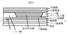
実施例1〜11で適用する画素の例を図18〜21に示す。図18の平面図のA−A’,B−B’,C−C’部の模式断面図をそれぞれ図19,20,21に示す。
【0083】
図18は自発光素子の例であり、有機EL素子の例である。
図に有機EL素子の画素構造の一例を示す。
【0084】
基板の上に直接あるいは絶縁膜を介してポリシリコン層が形成されている。その上にはゲート絶縁膜があり、該ゲート絶縁膜上にゲート電極が構成されている。ゲート電極形成後、イオンが打ち込まれることで、ポリシリコン層がゲート電極下以外の部分が低抵抗化されている。
【0085】
ポリシリコン層の一端はDLと一体のドレイン電極が、スルーホールによりポリシリコン層と接続している。ポリシリコン層の他端はソース電極が、スルーホールによりポリシリコン層と接続している。ソース電極は、下層電極と接続されている。
【0086】
図21から明らかなように、発光材料は画素に構成された穴の中に形成され、かつ上下をホール注入層を介在して下層電極と上層電極で挟まれている。
【0087】
ホール注入層は、発光材料層への電流の供給を円滑にする上で設けたものである。また穴は、バンク膜の非形成領域を設けることにより構成した物である。有機材料の発光材料層は、膜厚が必要である。また、低コスト化のためには、印刷法、熱転写法、あるいはインクジェット法で形成することが望ましい。むろんマスク蒸着でも良い。
【0088】
発光材料層は、その中を電流が通ることで、その電気エネルギーを光エネルギーに変換することにより発光する。そのメカニズムの一例は、電気エネルギーにより励起した発光中心が、光エネルギーとしてエネルギーを放出しその励起状態から基底状態に戻ることにより実現する。したがって、発光材料層は導電性であるため、隣接する他の画素と発光材料層が接触すると短絡するため、これを防ぐことを容易とするため設けるものであり、また同時に発光材料層の形成部と非形成部の段差を低減するものでもある。
【0089】
次に、動作を説明する。ゲートがON状態になると、DLからの電流はゲート電極下にチャネル層が形成されることにより、ソース電極へと流れる。これは、ソース電極に接続された下層電極からホール注入層を介して発光材料層を通り、上層電極へと流れる。これにより、発光が行われる。
【0090】
そして上層電極及び下層電極の少なくとも一方を透明電極としておくことで、その光を外部に放射し、表示装置が実現できる。透明電極としてはITO(Indium−Tin−Oxide)、IZO(Indium−Zinc−Oxide)、ITZO(Inzium−Tin−Zinc−Oxide),In2O3、SnO2などが知られている。
【0091】
有機EL素子は、液晶表示素子のような電圧駆動型と異なり、電流駆動型である。すなわち、電流量により発光を制御する。このため、明るい画像表示装置を得るには電流を多く流す必要がある。
【0092】
実施例1〜11の構成では各色間の電流を平均化でき、色むら、輝度むらの低減が実現する。またDummy期間以外にもGLのON状態を設けることで、電流の書込み時間が長くなり、より大電流が画素に供給できるようになり、明るく、色むらのない、辞発光型の画像表示装置が実現する。
【0093】
【発明の効果】
以上詳述したように、本発明の画像表示装置により、隣接画素間で極性を反転させ、かつ有効表示領域外寸法を縮小し、低消費電力で、色むらが少なく、輝度むらが少なく、書込み特性に優れた画像装置を提供することができる。特に、液晶表示装置、有機EL表示装置を提供できる。
【図面の簡単な説明】
【図1】本発明の一実施例による画像表示装置の模式回路図である。
【図2】本発明の一実施例による画像表示装置の信号極性を示す説明図である。
【図3】本発明の他の実施例による画像表示装置の信号極性を示す説明図である。
【図4】本発明の他の実施例による画像表示装置の信号極性を示す説明図である。
【図5】本発明の他の実施例による画像表示装置の模式回路図である。
【図6】本発明の他の実施例による画像表示装置の信号極性を示す説明図である。
【図7】本発明の他の実施例による画像表示装置の信号極性を示す説明図である。
【図8】本発明の他の実施例による画像表示装置の構成図である。
【図9】本発明の他の実施例による画像表示装置の構成図である。
【図10】本発明の他の実施例による画像表示装置の構成図である。
【図11】本発明の他の実施例による画像表示装置の構成図である。
【図12】本発明の他の実施例による画像表示装置の構成図である。
【図13】本発明の他の実施例による画像表示装置の構成図である。
【図14】本発明の他の実施例による画像表示装置の断面構成図である。
【図15】本発明の他の実施例による画像表示装置の断面構成図である。
【図16】本発明の画像表示装置に用いる液晶表示素子の画素の模式説明図である。
【図17】本発明の画像表示装置に用いる液晶表示素子の画素の模式説明図である。
【図18】本発明の画像表示装置に用いる自発光素子の画素の模式説明図である。
【図19】本発明の画像表示装置に用いる自発光素子の画素の断面説明図である。
【図20】本発明の画像表示装置に用いる自発光素子の画素の断面説明図である。
【図21】本発明の画像表示装置に用いる自発光素子の画素の断面説明図である。
【符号の説明】
TH…スルーホール、TCON…TFTコントローラ、FPC…フレキシブルプリント基板、PCB…プリント基板、TCP…テープキャリアパッケージ、PX…画素電極、CT…共通電極、CL…基準信号線。
Claims (4)
- 映像信号生成回路後に分配回路を有する画像表示装置において、
前記映像信号生成回路からの第1の出力(D1)と第2の出力(D2)を有し、該第1の出力(D1)と第2の出力(D2)は極性が反転したものであり、
順に並設される複数の映像信号線R1、G1、B1、R2、G2、B2を有し、
前記分配回路により前記第1の出力(D1)が前記映像信号線R1、B1、G2に接続し、前記第2の出力(D2)が前記映像信号線G1、R2、B2に接続し、
順に併設する第1の配線と第2の配線と第3の配線を有し、前記選択回路は前記第1の配線にONかOFFの信号を供給する第1のSW回路(SL1)と、前記第2の配線にONかOFFの信号を供給する第2のSW回路(SL2)と、前記第3の配線にONかOFFの信号を供給する第3のSW回路(SL3)とを有し、
前記映像信号線R1は前記第1の配線により制御されるスイッチを介して前記第1の出力(D1)と接続し、
前記映像信号線G1は前記第2の配線により制御されるスイッチを介して前記第2の出力(D2)と接続し、
前記映像信号線B1は前記第3の配線により制御されるスイッチを介して前記第1の出力(D1)と接続し、
前記映像信号線R2は前記第1の配線により制御されるスイッチを介して前記第2の出力(D2)と接続し、
前記映像信号線G2は前記第2の配線により制御されるスイッチを介して前記第1の出力(D1)と接続し、
前記映像信号線B2は前記第3の配線により制御されるスイッチを介して前記第2の出力(D2)と接続することを特徴とする画像表示装置。 - 前記第1の出力(D1)へは、前記映像信号線R1に対応するデータ、前記映像信号線G2に対応するデータ、前記映像信号線B1に対応するデータの順に送られ、前記第2の出力(D2)には、前記映像信号線R2に対応するデータ、前記映像信号線G1に対応するデータ、前記映像信号線B2に対応するデータの順に送られることを特徴とする請求項1記載の画像表示装置。
- 映像信号生成回路後に分配回路を有する画像表示装置において、
前記映像信号生成回路からの第1の出力(D1)と第2の出力(D2)を有し、該第1の出力(D1)と第2の出力(D2)は極性が反転したものであり、
順に並設される複数の映像信号線R1、G1、B1、R2、G2、B2を有し、
前記分配回路により前記第1の出力(D1)が前記映像信号線R1、B1、R2に接続し、前記第2の出力(D2)が前記映像信号線G1、G2、B2に接続し、
順に併設する第1の配線と第2の配線と第3の配線を有し、前記選択回路は前記第1の配線にONかOFFの信号を供給する第1のSW回路(SL1)と、前記第2の配線にONかOFFの信号を供給する第2のSW回路(SL2)と、前記第3の配線にONかOFFの信号を供給する第3のSW回路(SL3)とを有し、
前記映像信号線R1は前記第1の配線により制御されるスイッチを介して前記第1の出力(D1)と接続し、
前記映像信号線G1は前記第2の配線により制御されるスイッチを介して前記第2の出力(D2)と接続し、
前記映像信号線B1は前記第3の配線により制御されるスイッチを介して前記第1の出力(D1)と接続し、
前記映像信号線R2は前記第2の配線により制御されるスイッチを介して前記第1の出力(D1)と接続し、
前記映像信号線G2は前記第3の配線により制御されるスイッチを介して前記第2の出力(D2)と接続し、
前記映像信号線B2は前記第1の配線により制御されるスイッチを介して前記第2の出力(D2)と接続することを特徴とする画像表示装置。 - 前記第1の出力(D1)へは、前記映像信号線R1に対応するデータ、前記映像信号線R2に対応するデータ、前記映像信号線B1に対応するデータの順に送られ、前記第2の出力(D2)には、前記映像信号線B2に対応するデータ、前記映像信号線G1に対応するデータ、前記映像信号線G2に対応するデータの順に送られることを特徴とする請求項3記載の画像表示装置。
Priority Applications (2)
| Application Number | Priority Date | Filing Date | Title |
|---|---|---|---|
| JP2001342657A JP3819760B2 (ja) | 2001-11-08 | 2001-11-08 | 画像表示装置 |
| US10/270,295 US6985130B2 (en) | 2001-11-08 | 2002-10-15 | Display device including a distribution circuit disposed after a video signal generation circuit |
Applications Claiming Priority (1)
| Application Number | Priority Date | Filing Date | Title |
|---|---|---|---|
| JP2001342657A JP3819760B2 (ja) | 2001-11-08 | 2001-11-08 | 画像表示装置 |
Publications (2)
| Publication Number | Publication Date |
|---|---|
| JP2003140626A JP2003140626A (ja) | 2003-05-16 |
| JP3819760B2 true JP3819760B2 (ja) | 2006-09-13 |
Family
ID=19156476
Family Applications (1)
| Application Number | Title | Priority Date | Filing Date |
|---|---|---|---|
| JP2001342657A Expired - Fee Related JP3819760B2 (ja) | 2001-11-08 | 2001-11-08 | 画像表示装置 |
Country Status (2)
| Country | Link |
|---|---|
| US (1) | US6985130B2 (ja) |
| JP (1) | JP3819760B2 (ja) |
Families Citing this family (58)
| Publication number | Priority date | Publication date | Assignee | Title |
|---|---|---|---|---|
| FR2803082B1 (fr) * | 1999-12-28 | 2002-03-22 | Trixell Sas | Procede de compensation en temperature de la sensibilite d'un detecteur d'image |
| JP2004037498A (ja) * | 2002-06-28 | 2004-02-05 | Seiko Epson Corp | 電気光学装置の駆動回路、電気光学装置、電子機器及び電気光学装置の駆動方法 |
| US7369111B2 (en) * | 2003-04-29 | 2008-05-06 | Samsung Electronics Co., Ltd. | Gate driving circuit and display apparatus having the same |
| JP4168339B2 (ja) | 2003-12-26 | 2008-10-22 | カシオ計算機株式会社 | 表示駆動装置及びその駆動制御方法並びに表示装置 |
| JP4694134B2 (ja) * | 2004-03-09 | 2011-06-08 | 株式会社 日立ディスプレイズ | 表示装置 |
| KR20050102385A (ko) * | 2004-04-22 | 2005-10-26 | 엘지.필립스 엘시디 주식회사 | 일렉트로-루미네센스 표시장치 |
| KR100649249B1 (ko) * | 2004-06-30 | 2006-11-24 | 삼성에스디아이 주식회사 | 역다중화 장치와, 이를 이용한 발광 표시 장치 및 그 표시패널 |
| KR101044920B1 (ko) * | 2004-07-28 | 2011-06-28 | 엘지디스플레이 주식회사 | 액정표시장치용 게이트 구동회로 및 이를 이용한액정표시장치 |
| US8199079B2 (en) * | 2004-08-25 | 2012-06-12 | Samsung Mobile Display Co., Ltd. | Demultiplexing circuit, light emitting display using the same, and driving method thereof |
| KR100662978B1 (ko) * | 2004-08-25 | 2006-12-28 | 삼성에스디아이 주식회사 | 발광 표시장치와 그의 구동방법 |
| AU2005203198A1 (en) * | 2004-08-27 | 2006-03-16 | Idc, Llc | Staggered column drive circuit systems and methods |
| US7499208B2 (en) * | 2004-08-27 | 2009-03-03 | Udc, Llc | Current mode display driver circuit realization feature |
| KR100583138B1 (ko) * | 2004-10-08 | 2006-05-23 | 삼성에스디아이 주식회사 | 발광 표시장치 |
| KR100604053B1 (ko) | 2004-10-13 | 2006-07-24 | 삼성에스디아이 주식회사 | 발광 표시장치 |
| JP4206087B2 (ja) * | 2004-10-13 | 2009-01-07 | 三星エスディアイ株式会社 | 発光表示装置 |
| JP4367386B2 (ja) | 2004-10-25 | 2009-11-18 | セイコーエプソン株式会社 | 電気光学装置、その駆動回路、駆動方法および電子機器 |
| CN100456353C (zh) * | 2004-10-25 | 2009-01-28 | 精工爱普生株式会社 | 电光装置、其驱动电路、驱动方法和电子设备 |
| KR100688800B1 (ko) * | 2004-11-17 | 2007-03-02 | 삼성에스디아이 주식회사 | 발광 표시장치와 그의 구동방법 |
| US20060114273A1 (en) * | 2004-11-29 | 2006-06-01 | Sanyo Electric Co., Ltd. | Display panel |
| US20060119557A1 (en) * | 2004-12-03 | 2006-06-08 | Toppoly Optoelectronics Corporation | System and method for driving an LCD |
| JP2006189806A (ja) * | 2004-12-06 | 2006-07-20 | Semiconductor Energy Lab Co Ltd | 表示装置及びその駆動方法 |
| JP2006267525A (ja) * | 2005-03-24 | 2006-10-05 | Renesas Technology Corp | 表示装置用駆動装置および表示装置用駆動方法 |
| WO2007013210A1 (ja) * | 2005-07-29 | 2007-02-01 | Sharp Kabushiki Kaisha | 表示装置 |
| KR100635509B1 (ko) * | 2005-08-16 | 2006-10-17 | 삼성에스디아이 주식회사 | 유기 전계발광 표시장치 |
| KR100666640B1 (ko) | 2005-09-15 | 2007-01-09 | 삼성에스디아이 주식회사 | 유기 전계발광 표시장치 |
| WO2007061863A2 (en) * | 2005-11-17 | 2007-05-31 | Mark Nelson | Electronic surveying method and system |
| US7633495B2 (en) * | 2006-02-14 | 2009-12-15 | Tpo Displays Corp. | Driving circuit with low power consumption multiplexer and a display panel and an electronic device using the same |
| JP2007241012A (ja) * | 2006-03-10 | 2007-09-20 | Casio Comput Co Ltd | 表示装置及びその駆動制御方法 |
| KR100784014B1 (ko) * | 2006-04-17 | 2007-12-07 | 삼성에스디아이 주식회사 | 유기전계발광 표시장치 및 그의 구동방법 |
| JP5233080B2 (ja) * | 2006-05-10 | 2013-07-10 | セイコーエプソン株式会社 | 電気光学装置及び電子機器 |
| JP2008292837A (ja) * | 2007-05-25 | 2008-12-04 | Hitachi Displays Ltd | 表示装置 |
| US8300032B2 (en) * | 2007-09-05 | 2012-10-30 | Himax Technologies Limited | Method for transmitting image data to driver of display |
| US20090115700A1 (en) * | 2007-11-02 | 2009-05-07 | Epson Imaging Devices Corporation | Liquid crystal display device |
| JP2009139774A (ja) * | 2007-12-10 | 2009-06-25 | Hitachi Displays Ltd | 表示装置 |
| JP2009168849A (ja) * | 2008-01-10 | 2009-07-30 | Seiko Epson Corp | 電気光学装置、電気光学装置の駆動方法、電子機器 |
| JP5359141B2 (ja) * | 2008-02-06 | 2013-12-04 | セイコーエプソン株式会社 | 電気光学装置、その駆動方法、電子機器 |
| JP2009198765A (ja) * | 2008-02-21 | 2009-09-03 | Seiko Epson Corp | 電気光学装置及びその駆動方法、電気光学装置用駆動回路並びに電子機器 |
| JP5285934B2 (ja) * | 2008-03-11 | 2013-09-11 | 株式会社ジャパンディスプレイ | 液晶表示装置 |
| TWI387956B (zh) * | 2008-03-12 | 2013-03-01 | Au Optronics Corp | 實現點反轉的資料多工器架構之液晶顯示裝置及其驅動方法 |
| JP5035165B2 (ja) * | 2008-07-28 | 2012-09-26 | カシオ計算機株式会社 | 表示駆動装置及び表示装置 |
| KR100983392B1 (ko) * | 2008-08-19 | 2010-09-20 | 매그나칩 반도체 유한회사 | 칼럼 데이터 구동회로, 이를 구비한 표시장치 및 그의 구동방법 |
| TWI404028B (zh) * | 2008-09-01 | 2013-08-01 | Au Optronics Corp | 一種液晶顯示裝置之影像優化方法 |
| KR100962921B1 (ko) * | 2008-11-07 | 2010-06-10 | 삼성모바일디스플레이주식회사 | 유기전계발광표시장치 |
| JP2010191444A (ja) * | 2010-03-18 | 2010-09-02 | Hitachi Displays Ltd | 表示装置 |
| KR101982716B1 (ko) * | 2012-02-28 | 2019-05-29 | 삼성디스플레이 주식회사 | 표시장치 |
| KR102035718B1 (ko) * | 2012-11-26 | 2019-10-24 | 삼성디스플레이 주식회사 | 유기전계발광 표시장치 및 그의 구동방법 |
| KR102298849B1 (ko) * | 2014-12-31 | 2021-09-09 | 엘지디스플레이 주식회사 | 표시장치 |
| US10896650B2 (en) * | 2016-06-01 | 2021-01-19 | Sharp Kabushiki Kaisha | Video signal line drive circuit, display device including same, and drive method for video signal line |
| CN105867040A (zh) * | 2016-06-23 | 2016-08-17 | 武汉华星光电技术有限公司 | 阵列基板及其液晶显示面板 |
| WO2018173280A1 (ja) | 2017-03-24 | 2018-09-27 | シャープ株式会社 | 表示装置およびその駆動方法 |
| US20200135110A1 (en) * | 2017-03-24 | 2020-04-30 | Sharp Kabushiki Kaisha | Display device and driving method therefor |
| US10996528B2 (en) * | 2017-06-22 | 2021-05-04 | Sakai Display Products Corporation | Display device |
| US10789873B2 (en) * | 2017-08-23 | 2020-09-29 | HKC Corporation Limited | Driving device and driving method of display device |
| TWI638216B (zh) | 2017-10-30 | 2018-10-11 | 友達光電股份有限公司 | 顯示裝置 |
| CN108630146B (zh) * | 2018-05-14 | 2019-11-12 | 上海天马有机发光显示技术有限公司 | 阵列基板的驱动方法、有机发光显示面板和显示装置 |
| CN109036292B (zh) * | 2018-09-21 | 2021-01-26 | 京东方科技集团股份有限公司 | 显示方法和显示装置 |
| CN109256081B (zh) * | 2018-11-16 | 2022-04-08 | 京东方科技集团股份有限公司 | 一种源极驱动电路、显示面板 |
| CN112885850B (zh) * | 2021-01-29 | 2024-04-05 | 合肥京东方卓印科技有限公司 | 显示面板、显示装置 |
Family Cites Families (5)
| Publication number | Priority date | Publication date | Assignee | Title |
|---|---|---|---|---|
| JP2850728B2 (ja) * | 1993-11-15 | 1999-01-27 | 株式会社デンソー | El表示装置の駆動装置及び駆動方法 |
| JPH11249627A (ja) | 1998-03-04 | 1999-09-17 | Sony Corp | 液晶表示装置 |
| JPH11327518A (ja) | 1998-03-19 | 1999-11-26 | Sony Corp | 液晶表示装置 |
| JPH11338423A (ja) * | 1998-05-15 | 1999-12-10 | Internatl Business Mach Corp <Ibm> | カラー表示方法、この表示方法に適するマトリックス駆動用液晶表示モジュール、及び、この液晶表示モジュールを含むpcシステム、並びに、プロジェクションタイプ表示装置 |
| JP2001109435A (ja) | 1999-10-05 | 2001-04-20 | Toshiba Corp | 表示装置 |
-
2001
- 2001-11-08 JP JP2001342657A patent/JP3819760B2/ja not_active Expired - Fee Related
-
2002
- 2002-10-15 US US10/270,295 patent/US6985130B2/en not_active Expired - Lifetime
Also Published As
| Publication number | Publication date |
|---|---|
| US6985130B2 (en) | 2006-01-10 |
| JP2003140626A (ja) | 2003-05-16 |
| US20030085885A1 (en) | 2003-05-08 |
Similar Documents
| Publication | Publication Date | Title |
|---|---|---|
| JP3819760B2 (ja) | 画像表示装置 | |
| KR101204365B1 (ko) | 액정 표시 패널 및 그 제조 방법 | |
| KR101196860B1 (ko) | 액정 표시 장치 | |
| US8416168B2 (en) | Liquid crystal display | |
| KR101400384B1 (ko) | 액정표시장치 | |
| US20090195492A1 (en) | Liquid crystal display device | |
| KR20140147932A (ko) | 액정 디스플레이 장치와 이의 구동방법 | |
| KR101931248B1 (ko) | 표시장치 및 그 제조방법 | |
| CN103926772B (zh) | Tft阵列基板、显示面板和显示装置 | |
| KR101100883B1 (ko) | 박막 트랜지스터 표시판 | |
| US7403193B2 (en) | Image display device | |
| JP4702114B2 (ja) | デマルチプレクサ、電気光学装置および電子機器 | |
| KR20060070346A (ko) | 표시 장치 | |
| KR20080002336A (ko) | 액정표시장치 | |
| KR20060085289A (ko) | 듀얼 표시 장치 | |
| JP4128045B2 (ja) | 有機elパネル | |
| KR102404392B1 (ko) | 협 베젤 구조를 갖는 대형 액정 표시장치 | |
| KR20060020174A (ko) | 가요성 인쇄 회로 기판, 테이프 캐리어 패키지 및 이를포함하는 표시 장치 | |
| KR101006441B1 (ko) | 액정 표시판 조립체 및 액정 표시 장치 | |
| KR20070070748A (ko) | 액정표시장치 | |
| KR20040015595A (ko) | 액정 표시 장치 | |
| KR20060060869A (ko) | 표시 장치 | |
| CN113707095A (zh) | 显示装置 | |
| US20110216103A1 (en) | Liquid crystal display device | |
| KR20060079698A (ko) | 액정 표시 장치 |
Legal Events
| Date | Code | Title | Description |
|---|---|---|---|
| A621 | Written request for application examination |
Free format text: JAPANESE INTERMEDIATE CODE: A621 Effective date: 20040310 |
|
| RD02 | Notification of acceptance of power of attorney |
Free format text: JAPANESE INTERMEDIATE CODE: A7422 Effective date: 20040310 |
|
| RD04 | Notification of resignation of power of attorney |
Free format text: JAPANESE INTERMEDIATE CODE: A7424 Effective date: 20040312 |
|
| A977 | Report on retrieval |
Free format text: JAPANESE INTERMEDIATE CODE: A971007 Effective date: 20050615 |
|
| A131 | Notification of reasons for refusal |
Free format text: JAPANESE INTERMEDIATE CODE: A131 Effective date: 20050621 |
|
| A521 | Request for written amendment filed |
Free format text: JAPANESE INTERMEDIATE CODE: A523 Effective date: 20050816 |
|
| A131 | Notification of reasons for refusal |
Free format text: JAPANESE INTERMEDIATE CODE: A131 Effective date: 20060322 |
|
| A521 | Request for written amendment filed |
Free format text: JAPANESE INTERMEDIATE CODE: A523 Effective date: 20060518 |
|
| TRDD | Decision of grant or rejection written | ||
| A01 | Written decision to grant a patent or to grant a registration (utility model) |
Free format text: JAPANESE INTERMEDIATE CODE: A01 Effective date: 20060613 |
|
| A61 | First payment of annual fees (during grant procedure) |
Free format text: JAPANESE INTERMEDIATE CODE: A61 Effective date: 20060615 |
|
| R150 | Certificate of patent or registration of utility model |
Ref document number: 3819760 Country of ref document: JP Free format text: JAPANESE INTERMEDIATE CODE: R150 |
|
| FPAY | Renewal fee payment (event date is renewal date of database) |
Free format text: PAYMENT UNTIL: 20090623 Year of fee payment: 3 |
|
| FPAY | Renewal fee payment (event date is renewal date of database) |
Free format text: PAYMENT UNTIL: 20100623 Year of fee payment: 4 |
|
| FPAY | Renewal fee payment (event date is renewal date of database) |
Free format text: PAYMENT UNTIL: 20100623 Year of fee payment: 4 |
|
| FPAY | Renewal fee payment (event date is renewal date of database) |
Free format text: PAYMENT UNTIL: 20110623 Year of fee payment: 5 |
|
| FPAY | Renewal fee payment (event date is renewal date of database) |
Free format text: PAYMENT UNTIL: 20110623 Year of fee payment: 5 |
|
| S531 | Written request for registration of change of domicile |
Free format text: JAPANESE INTERMEDIATE CODE: R313531 |
|
| FPAY | Renewal fee payment (event date is renewal date of database) |
Free format text: PAYMENT UNTIL: 20110623 Year of fee payment: 5 |
|
| R371 | Transfer withdrawn |
Free format text: JAPANESE INTERMEDIATE CODE: R371 |
|
| FPAY | Renewal fee payment (event date is renewal date of database) |
Free format text: PAYMENT UNTIL: 20110623 Year of fee payment: 5 |
|
| S111 | Request for change of ownership or part of ownership |
Free format text: JAPANESE INTERMEDIATE CODE: R313111 |
|
| S631 | Written request for registration of reclamation of domicile |
Free format text: JAPANESE INTERMEDIATE CODE: R313631 |
|
| FPAY | Renewal fee payment (event date is renewal date of database) |
Free format text: PAYMENT UNTIL: 20110623 Year of fee payment: 5 |
|
| R350 | Written notification of registration of transfer |
Free format text: JAPANESE INTERMEDIATE CODE: R350 |
|
| S111 | Request for change of ownership or part of ownership |
Free format text: JAPANESE INTERMEDIATE CODE: R313121 Free format text: JAPANESE INTERMEDIATE CODE: R313115 |
|
| FPAY | Renewal fee payment (event date is renewal date of database) |
Free format text: PAYMENT UNTIL: 20110623 Year of fee payment: 5 |
|
| R250 | Receipt of annual fees |
Free format text: JAPANESE INTERMEDIATE CODE: R250 |
|
| FPAY | Renewal fee payment (event date is renewal date of database) |
Free format text: PAYMENT UNTIL: 20120623 Year of fee payment: 6 |
|
| R350 | Written notification of registration of transfer |
Free format text: JAPANESE INTERMEDIATE CODE: R350 |
|
| FPAY | Renewal fee payment (event date is renewal date of database) |
Free format text: PAYMENT UNTIL: 20120623 Year of fee payment: 6 |
|
| FPAY | Renewal fee payment (event date is renewal date of database) |
Free format text: PAYMENT UNTIL: 20130623 Year of fee payment: 7 |
|
| R250 | Receipt of annual fees |
Free format text: JAPANESE INTERMEDIATE CODE: R250 |
|
| R250 | Receipt of annual fees |
Free format text: JAPANESE INTERMEDIATE CODE: R250 |
|
| R250 | Receipt of annual fees |
Free format text: JAPANESE INTERMEDIATE CODE: R250 |
|
| R250 | Receipt of annual fees |
Free format text: JAPANESE INTERMEDIATE CODE: R250 |
|
| R250 | Receipt of annual fees |
Free format text: JAPANESE INTERMEDIATE CODE: R250 |
|
| R250 | Receipt of annual fees |
Free format text: JAPANESE INTERMEDIATE CODE: R250 |
|
| R250 | Receipt of annual fees |
Free format text: JAPANESE INTERMEDIATE CODE: R250 |
|
| R250 | Receipt of annual fees |
Free format text: JAPANESE INTERMEDIATE CODE: R250 |
|
| R250 | Receipt of annual fees |
Free format text: JAPANESE INTERMEDIATE CODE: R250 |
|
| S531 | Written request for registration of change of domicile |
Free format text: JAPANESE INTERMEDIATE CODE: R313531 |
|
| S533 | Written request for registration of change of name |
Free format text: JAPANESE INTERMEDIATE CODE: R313533 |
|
| LAPS | Cancellation because of no payment of annual fees | ||
| R350 | Written notification of registration of transfer |
Free format text: JAPANESE INTERMEDIATE CODE: R350 |