JP3707765B2 - Field effect semiconductor device - Google Patents
Field effect semiconductor device Download PDFInfo
- Publication number
- JP3707765B2 JP3707765B2 JP25605199A JP25605199A JP3707765B2 JP 3707765 B2 JP3707765 B2 JP 3707765B2 JP 25605199 A JP25605199 A JP 25605199A JP 25605199 A JP25605199 A JP 25605199A JP 3707765 B2 JP3707765 B2 JP 3707765B2
- Authority
- JP
- Japan
- Prior art keywords
- layer
- impurity concentration
- barrier layer
- algaas
- barrier
- Prior art date
- Legal status (The legal status is an assumption and is not a legal conclusion. Google has not performed a legal analysis and makes no representation as to the accuracy of the status listed.)
- Expired - Lifetime
Links
- 239000004065 semiconductor Substances 0.000 title claims description 21
- 230000005669 field effect Effects 0.000 title claims description 14
- 230000004888 barrier function Effects 0.000 claims description 102
- 229910000980 Aluminium gallium arsenide Inorganic materials 0.000 claims description 70
- 239000012535 impurity Substances 0.000 claims description 47
- 238000009792 diffusion process Methods 0.000 claims description 4
- 235000018936 Vitellaria paradoxa Nutrition 0.000 claims description 2
- 108091006146 Channels Proteins 0.000 description 39
- 238000011979 disease modifying therapy Methods 0.000 description 30
- 229910001218 Gallium arsenide Inorganic materials 0.000 description 14
- 125000002103 4,4'-dimethoxytriphenylmethyl group Chemical group [H]C1=C([H])C([H])=C(C([H])=C1[H])C(*)(C1=C([H])C([H])=C(OC([H])([H])[H])C([H])=C1[H])C1=C([H])C([H])=C(OC([H])([H])[H])C([H])=C1[H] 0.000 description 12
- 238000010586 diagram Methods 0.000 description 12
- 229910000530 Gallium indium arsenide Inorganic materials 0.000 description 9
- 238000005530 etching Methods 0.000 description 7
- 239000000758 substrate Substances 0.000 description 7
- 239000000463 material Substances 0.000 description 6
- 230000000903 blocking effect Effects 0.000 description 4
- 238000000034 method Methods 0.000 description 4
- 230000001681 protective effect Effects 0.000 description 4
- 230000000694 effects Effects 0.000 description 2
- 238000010438 heat treatment Methods 0.000 description 2
- 238000002488 metal-organic chemical vapour deposition Methods 0.000 description 2
- 102000004129 N-Type Calcium Channels Human genes 0.000 description 1
- 108090000699 N-Type Calcium Channels Proteins 0.000 description 1
- 239000000969 carrier Substances 0.000 description 1
- 230000015556 catabolic process Effects 0.000 description 1
- 238000010030 laminating Methods 0.000 description 1
- 230000005533 two-dimensional electron gas Effects 0.000 description 1
Images


Classifications
-
- H—ELECTRICITY
- H10—SEMICONDUCTOR DEVICES; ELECTRIC SOLID-STATE DEVICES NOT OTHERWISE PROVIDED FOR
- H10D—INORGANIC ELECTRIC SEMICONDUCTOR DEVICES
- H10D30/00—Field-effect transistors [FET]
- H10D30/80—FETs having rectifying junction gate electrodes
- H10D30/801—FETs having heterojunction gate electrodes
-
- H—ELECTRICITY
- H10—SEMICONDUCTOR DEVICES; ELECTRIC SOLID-STATE DEVICES NOT OTHERWISE PROVIDED FOR
- H10D—INORGANIC ELECTRIC SEMICONDUCTOR DEVICES
- H10D30/00—Field-effect transistors [FET]
- H10D30/40—FETs having zero-dimensional [0D], one-dimensional [1D] or two-dimensional [2D] charge carrier gas channels
- H10D30/47—FETs having zero-dimensional [0D], one-dimensional [1D] or two-dimensional [2D] charge carrier gas channels having 2D charge carrier gas channels, e.g. nanoribbon FETs or high electron mobility transistors [HEMT]
- H10D30/471—High electron mobility transistors [HEMT] or high hole mobility transistors [HHMT]
- H10D30/473—High electron mobility transistors [HEMT] or high hole mobility transistors [HHMT] having confinement of carriers by multiple heterojunctions, e.g. quantum well HEMT
- H10D30/4732—High electron mobility transistors [HEMT] or high hole mobility transistors [HHMT] having confinement of carriers by multiple heterojunctions, e.g. quantum well HEMT using Group III-V semiconductor material
- H10D30/4738—High electron mobility transistors [HEMT] or high hole mobility transistors [HHMT] having confinement of carriers by multiple heterojunctions, e.g. quantum well HEMT using Group III-V semiconductor material having multiple donor layers
-
- H—ELECTRICITY
- H10—SEMICONDUCTOR DEVICES; ELECTRIC SOLID-STATE DEVICES NOT OTHERWISE PROVIDED FOR
- H10D—INORGANIC ELECTRIC SEMICONDUCTOR DEVICES
- H10D30/00—Field-effect transistors [FET]
- H10D30/40—FETs having zero-dimensional [0D], one-dimensional [1D] or two-dimensional [2D] charge carrier gas channels
- H10D30/47—FETs having zero-dimensional [0D], one-dimensional [1D] or two-dimensional [2D] charge carrier gas channels having 2D charge carrier gas channels, e.g. nanoribbon FETs or high electron mobility transistors [HEMT]
- H10D30/471—High electron mobility transistors [HEMT] or high hole mobility transistors [HHMT]
- H10D30/475—High electron mobility transistors [HEMT] or high hole mobility transistors [HHMT] having wider bandgap layer formed on top of lower bandgap active layer, e.g. undoped barrier HEMTs such as i-AlGaN/GaN HEMTs
- H10D30/4755—High electron mobility transistors [HEMT] or high hole mobility transistors [HHMT] having wider bandgap layer formed on top of lower bandgap active layer, e.g. undoped barrier HEMTs such as i-AlGaN/GaN HEMTs having wide bandgap charge-carrier supplying layers, e.g. modulation doped HEMTs such as n-AlGaAs/GaAs HEMTs
Landscapes
- Junction Field-Effect Transistors (AREA)
Description
【0001】
【発明の属する技術分野】
本発明は半導体装置に関し、特にHEMT構造やDCHFET構造等のヘテロ接合構造を有する電界効果型半導体装置に関する。
【0002】
【従来の技術】
従来からマイクロ波帯〜ミリ波帯の領域で動作するトランジスタ素子としては、ヘテロ接合構造の電界効果トランジスタ(以下、ヘテロ接合FETという)が用いられている。このヘテロ接合FETは、そのドーピング構造によって、変調ドープ構造を用いたHEMT(高電子移動度トランジスタ)と、チャネルドープ構造を用いたDCHFET(ドープチャネルヘテロFET)とに大別される。なお、後者のDCHFETは、別称としてDMT、MISFET、HIGFETなどと呼ばれる。
【0003】
図1は従来のHEMTの積層構造を模式的に示す断面図である。このHEMT1においては、GaAs基板2の上にバッファ層3が形成され、バッファ層3の上にノンドープInGaAsのチャネル層4が形成され、チャネル層4の上には障壁層5が積層されている。障壁層5は、図1ではn型AlGaAs層5aとノンドープAlGaAs層5bの2層構造となっているが、ノンドープAlGaAs層/n型AlGaAs層/ノンドープAlGaAs層などの多層構造の場合もあり、n型AlGaAs層のみの場合もある。障壁層5の上には、ソース電極8及びドレイン電極9と良好なオーミック接合を得るため、n型GaAsからなるコンタクト層6が形成されている。コンタクト層6の上面には、ソース電極8及びドレイン電極9が形成されており、熱処理によってコンタクト層6とオーミック接合されている。
【0004】
ソース電極8及びドレイン電極9間においては、コンタクト層6をリセスエッチングすることにより、リセス7内に障壁層5のノンドープAlGaAs層5bを露出させている。このリセスエッチングは、AlGaAsをエッチングしないが、GaAsをエッチングするエッチャントを用いてコンタクト層6を選択的にエッチング除去し、ノンドープAlGaAs層5bでエッチング停止させることにより行われる。ゲート電極10は、リセス7内においてコンタクト層6から露出したノンドープAlGaAs層5bの上面に形成され、ノンドープAlGaAs層5bとショットキー接合している。また、HEMT1の表面は、SiN保護膜11によって覆われる。
【0005】
このようなHEMT構造においては、ソース及びドレイン電極8、9の下方におけるエネルギーバンド構造(伝導帯の底)とゲート電極10の下方におけるエネルギーバンド構造(伝導帯の底)はそれぞれ図2(a)(b)に示すようになっており、n型AlGaAs層5aの電子はAlGaAsとInGaAsの間のヘテロ接合を越えてエネルギー的に低いチャネル層4側へ移動する。こうして障壁層5から高純度のチャネル層4へ供給された電子(2次元電子ガス)は、障壁層5のドナーによって散乱されることなくドリフトできるので、大きな移動度を持つことになる。すなわち、チャネル層4は電子が走行するチャネルとして働き、障壁層5はチャネル層に電子を供給する供給源として働き、ソース電極8とドレイン電極9の間に電位差が与えられると、チャネル層4にドレイン電流が流れる。
【0006】
図3は従来のDCHFETのうちのDMTの積層構造を模式的に示す断面図である。このDMT21においては、半絶縁性GaAs基板22の上にバッファ層23が形成され、バッファ層23の上にn型InGaAsのチャネル層24が形成され、チャネル層24の上には障壁層25が積層されている。障壁層25は、DMT構造では、ノンドープAlGaAsによって形成されている。障壁層25の上には、ソース電極28及びドレイン電極29と良好なオーミック接合を得るため、n型GaAsからなるコンタクト層26が形成されている。コンタクト層26の上面には、ソース電極28及びドレイン電極29が形成されており、熱処理によってコンタクト層26とオーミック接合されている。
【0007】
ソース電極28及びドレイン電極29の間においては、コンタクト層26を選択的にリセスエッチングすることにより、リセス27内に障壁層25を露出させている。ゲート電極30は、リセス27内においてコンタクト層26から露出した障壁層25の上面に形成され、障壁層25にショットキー接合している。また、DMT21の表面は、SiN保護膜31によって覆われる。
【0008】
このようなDMT構造では、ソース及びドレイン電極28、29の下方におけるエネルギーバンド構造(伝導帯の底)とゲート電極30の下方におけるエネルギーバンド構造(伝導帯の底)はそれぞれ図4(a)(b)に示すようになっている。ゲート電極30に電圧を印加しない状態では、n型のチャネル層24に電子が蓄積されており、この状態でソース電極28とドレイン電極29の間に電位差を与えると、キャリアである電子がソース電極28からドレイン電極29に移動してドレイン電流が流れる。
【0009】
【発明が解決しようとする課題】
上記のようなHEMT構造においても、またDMT構造においても、障壁層の機能の一つとしては、ゲート電極に対して障壁を形成することが挙げられる。すなわち、ゲート電極とチャネル層との間に高いエネルギー障壁が存在することによって(HEMTの場合を図2(b)に、DMTの場合を図4(b)に示す。)、電子が障壁層を越えて、あるいは障壁層をトンネルして移動しにくくなり、ゲート電極への電流リークが阻止される。よって、より高い電流値までチャネルを開口することができ、またより高いゲート耐圧が可能となり、高出力を達成することができる。
【0010】
障壁層のこのような電流阻止能力は、障壁層の障壁高さとその厚さにより決定される。ここで、障壁高さは、障壁層とゲート電極との仕事関数差によって決まる。また、障壁層の厚さは障壁層内の不純物濃度によって決まり、不純物濃度の低い層を障壁層とすることによって実効的な障壁層の厚さを増大させることができ、そのため障壁層の不純物濃度を低くすることによってゲート電極への電流阻止能力を大幅に高めることができる。
【0011】
しかし、その一方で、この障壁層はドレイン電極又はソース電極とチャネル層との間に電流を流すための経路となるから、ドレイン電流を流すうえでは大きな抵抗体となる。よって、ソース・ドレイン間の直列抵抗を低減しようとすれば、障壁層の不純物濃度を高くして低抵抗化しなければならない。
【0012】
従って、障壁層の電流阻止能力を高めるためには、障壁層の不純物濃度を低くしなければならないが、そうすると障壁層が高抵抗化してソース・ドレイン間の直列抵抗が大きくなる。逆に、ソース・ドレイン間の直列抵抗を小さくするためには、障壁層の不純物濃度を高くして低抵抗化しなければならないが、そうすると障壁層の電流阻止能力が低下し、ゲート電極への電流リークが増加する。
【0013】
このような技術的なトレードオフのため、高い障壁機能を有しつつも直列抵抗の低いヘテロ接合FET構造が求められているにもかかわらず、従来においては、このようなFETを作製することは困難であった。
【0014】
また、従来の構造では、コンタクト層を選択的にリセスエッチングする際、コンタクト層の横方向にもエッチングが進行することにより、ゲート電極の両脇に目あき部分(過剰エッチング部分)が発生する。DMTの場合を図5に示すように、この目空き領域32からは下方へ向けて空乏層33が長く延びるので、ソース及びドレイン電極28、29間における直列抵抗がより増大し、さらに素子のDC特性を悪化させている。
【0015】
本発明は上述の技術的問題点を解決するためになされたものであり、その目的とするところは、ゲート電極に対しては高い障壁機能を有しつつも、ソース及びドレイン電極に対しては直列抵抗の低い障壁層を有する電界効果型半導体装置を提供することにある。
【0016】
【課題を解決するための手段とその作用】
本発明に係る電界効果型半導体装置は、チャネル層の上に複数層からなる障壁層が形成され、該障壁層の上方に2つのオーミック電極が形成され、該オーミック電極間にショットキー電極が形成された電界効果型半導体装置において、前記障壁層は、前記チャネル層よりも電子親和力が小さく、AlGaAsからなる2層の高不純物濃度層とその間に挟まれたAlGaAsからなる低不純物濃度層とを含む3層構造であり、前記ショットキー電極は、前記高不純物濃度層の上に形成された後に熱拡散によってその下端部を前記高不純物濃度層に埋め込み、かつその底面を前記障壁層の低不純物濃度層に接触させているものである。ここでいう低不純物濃度層には、意図して不純物を注入していないノンドープ層も含む。
【0017】
このような構造の障壁層としては、特にn型障壁層、ノンドープ障壁層およびn型障壁層を順次積層して形成したものを挙げることができ、障壁層はAlGaAsによって構成する。また、チャネル層はノンドープの半導体層でもよく、高不純物濃度の半導体層としてもよい。
【0018】
このように障壁層が高抵抗の低不純物濃度層とその上層及び下層に位置する低抵抗の高不純物濃度層とからなっているので、オーミック電極の下方においては、低不純物濃度層において障壁が疑似的に低くなるので、障壁層の通過抵抗すなわちオーミック電極間の直列抵抗が低くなる。
【0019】
特に、このような効果は、高不純物濃度層の間に挟まれた低不純物濃度層の膜厚を2.5nm以上10nm以下にした時に著しい。
【0020】
また、本発明の電界効果型半導体装置において、前記ショットキー電極の底面を障壁層の低不純物濃度層に接触させているので、ショットキー電極の下方でショットキー障壁機能を高く保つことができるので、高い障壁機能を有しつつも直列抵抗の低いFET特性を実現することができる。
【0021】
さらに、ショットキー電極の下方に高濃度不純物濃度の障壁層が位置することにより、ショットキー電極の両側に目あき領域が発生した場合にも、空乏層の成長を抑制して直列抵抗の増大を抑えることができる。
【0022】
【発明の実施の形態】
(第1の実施形態)
図6は本発明の一実施形態によるHEMT41の構造を模式的に示す断面図である。このHEMT41においては、半絶縁性GaAs基板42の上にバッファ層43が形成され、バッファ層43の上にノンドープInGaAsのチャネル層44が10nmの膜厚に形成され、チャネル層44の上には複数層からなる障壁層(以下、多層障壁層という)45が形成されている。多層障壁層45は、図6では膜厚10nmのn型AlGaAs層45a(不純物濃度3×1018cm−3)、膜厚2.5〜5nmのノンドープAlGaAs層45b、膜厚10nmのn型AlGaAs層54c(不純物濃度3×1018cm−3)の3層構造となっている。多層障壁層45の上には、ソース電極48及びドレイン電極49と良好なオーミック接合を得るため、n+型GaAs(不純物濃度5×1018cm−3)からなる膜厚50nmのコンタクト層46が形成されており、コンタクト層46の上面にオーミック接触のソース電極48及びドレイン電極49が形成されている。これらバッファ層43、チャネル層44、多層障壁層45を構成する各半導体障壁層45a〜45c及びコンタクト層46は、MBE法、MOCVD法等を用いたエピタキシャル成長により、この順序で半絶縁性GaAs基板42上に形成される。
【0023】
コンタクト層46の上面には、コンタクト層46にオーミック接触するソース電極48及びドレイン電極49が形成されており、ソース及びドレイン電極48、49間でコンタクト層46は選択的にリセスエッチングされている。コンタクト層46を部分的に除去したリセス47内にはn型AlGaAs層45cが露出しており、ゲート電極50はこのn型AlGaAs層45cの上に形成された後、熱拡散によってその底面がノンドープAlGaAs層45bにショットキー接触させられる。この結果、ゲート電極50の下端部がn型AlGaAs層45c内に埋め込まれる。また、HEMT41は最終的には、SiN等の絶縁保護膜51で被覆される。
【0024】
このような構造のHEMT41におけるソース及びドレイン電極48、49の下方におけるエネルギーバンド構造(伝導帯の底)とゲート電極50の下方におけるエネルギーバンド構造(伝導帯の底)をそれぞれ図7(a)(b)に示す。ソース及びドレイン電極48、49の下方においては、多層障壁層45が高不純物濃度低抵抗のn型AlGaAs層45a、低不純物濃度高抵抗のノンドープAlGaAs層45b、高不純物濃度低抵抗のn型AlGaAs層45cから構成されているので、図7(a)に示すように、中央のノンドープAlGaAs層45bの障壁高さは、エネルギーバンド構造上電子に対して擬似的に低くなり、ソース及びドレイン電極48、49間における多層障壁層45の通過抵抗、すなわちソース及びドレイン電極48、49間の直列抵抗を低くすることができる。
【0025】
これに対し、ゲート電極50の下方においては、図7(b)に示すように、多層障壁層45はノンドープAlGaAs層45bとn型AlGaAs障壁層45aとからなり、従来例のHEMT1におけるゲート電極10の下方と同じ多層障壁層の構造となっている。
【0026】
従って、このHEMT41にあっては、n型AlGaAs層45aの不純物濃度を低くすることによってゲート電極50の下方におけるゲート障壁機能を高く保つことができ、しかも、ソース及びドレイン電極48、49の下方においては、ノンドープAlGaAs層45bによって障壁高さを実効的に低くすることができ、ソース及びドレイン電極48、49間における直列抵抗を小さくすることが可能になる。
【0027】
なお、図6の実施形態では、チャネル層44としてInGaAs層を用いているが、GaAsを用いてもよい。また、この実施形態では、チャネル層44にInGaAsを用い、多層障壁層45にAlGaAsを用いているが、チャネル層44の材料と多層障壁層45の材料とは、互いに電子親和力差が生じていればよく、InGaAg/InGaPなどの材料の組み合わせでもよい。また、チャネル層44上の多層障壁層45はノンドープAlGaAsから始めてもよく、例えばチャネル層の上にノンドープ(i)AlGaAs層/n型AlGaAs層/ノンドープ(i)AlGaAs層/n型AlGaAs層からなる多層障壁層を形成してもよい。なお、多層障壁層45を構成する半導体層の各膜厚に特に規定はないが、ノンドープAlGaAs層については膜厚10nm以下が好ましい。
【0028】
さらに、多層障壁層45は上記のような3層構造を繰り返した多層構造としてもよい。あるいは、チャネル層44の下面にも電子供給層を設けたダブルドープHEMT構造としてもよい。
【0030】
(第2の実施形態)
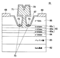
図8は本発明の別な実施形態によるDMTの構造を模式的に示す断面図である。このDMT61においては、半絶縁性GaAs基板62の上にバッファ層63が形成され、バッファ層63の上にn型InGaAs(不純物濃度2×1018cm−3)のチャネル層64が10nmの膜厚に形成され、チャネル層64の上には多層障壁層65が形成されている。多層障壁層65は、図8では膜厚10nmのn型AlGaAs層65a(不純物濃度3×1018cm−3)、膜厚2.5〜5nmのノンドープAlGaAs層65b、膜厚10nmのn型AlGaAs層65c(不純物濃度3×1018cm−3)の3層構造となっている。多層障壁層65の上には、ソース電極68及びドレイン電極69と良好なオーミック接合を得るため、n+型GaAs(不純物濃度5×1018cm−3)からなる膜厚50nmのコンタクト層66が形成されており、コンタクト層66の上面にオーミック接触のソース電極68及びドレイン電極69が形成されている。これらバッファ層63、チャネル64層、多層障壁層65を構成する各半導体層65a〜65c及びコンタクト66層は、MBE法、MOCVD法等を用いたエピタキシャル成長により、この順序で半絶縁性GaAs基板62上に形成される。
【0031】
コンタクト層66の上面には、コンタクト層66にオーミック接触するソース電極68及びドレイン電極69が形成されており、ソース及びドレイン電極68、69間のコンタクト層66はリセスエッチングによって選択的に除去されている。コンタクト層66を部分的に除去したリセス67内にはn型AlGaAs層65cが露出しており、ゲート電極70はこのn型AlGaAs層65cの上に形成された後、熱拡散によってその底面がノンドープAlGaAs層65bにショットキー接触させられる。この結果、ゲート電極70の下端部がn型AlGaAs層65c内に埋め込まれる。また、DMT61は最終的には、SiN等の絶縁保護膜71で被覆される。
【0032】
このような構造のDMT61におけるソース及びドレイン電極68、69の下方におけるエネルギーバンド構造(伝導帯の底)とゲート電極70の下方におけるエネルギーバンド構造(伝導帯の底)をそれぞれ図9(a)(b)に示す。ソース及びドレイン電極68、69の下方においては、多層障壁層65が高不純物濃度低抵抗のn型AlGaAs層65a、低不純物濃度高抵抗のノンドープAlGaAs層65b、高不純物濃度低抵抗のn型AlGaAs層65cから構成されているので、図9(a)に示すように、中央のノンドープAlGaAs層65bの障壁高さは、エネルギーバンド構造上電子に対して擬似的に低くなり、ソース及びドレイン電極68、69間における多層障壁層の通過抵抗、すなわちソース電極68及びドレイン電極69間の直列抵抗を低減することができる。
【0033】
これに対し、ゲート電極70の下方においては、図9(b)に示すように、多層障壁層65はノンドープAlGaAs層65bとn型AlGaAs層65aとからなり、n型AlGaAs層65aの不純物濃度を低くすることによってゲート障壁機能を高くすることができる。
【0034】
従って、このDMT61にあっても、n型AlGaAs層65a、65cの不純物濃度を低くすることによってゲート電極70の下方におけるゲート障壁機能を高く保つことができ、しかも、ソース及びドレイン電極68、69の下方においては、ノンドープAlGaAs層65bによって障壁高さを実効的に低くすることで直列抵抗を小さくすることが可能になる。
【0035】
また、従来のDMT21では、ゲート電極30とチャネル層24との間がノンドープAlGaAs層のみであったので、ゲート電極の両側に目あき領域が発生した場合には、図5に示したように空乏層33が下方へ長く延びていた。これに対し、このDMT61では、ゲート電極70とチャネル層64との間にn型AlGaAs層65a/ノンドープAlGaAs層65b/n型AlGaAs層65cからなる多層障壁層65が存在しているので、図10に示すように、ゲート電極70の両側に目あき領域72が発生しても空乏層73がn型AlGaAs層65cよりも下方へ延びにくく、目あき領域72によってソース及びドレイン電極68、69間の直流抵抗が増大するのを抑制できる。
【0036】
図11は上記のような構造の本発明実施例によるDMT(DCHFET)の電流電圧特性を従来例のDMTと比較して示した図である。この図においては、横軸はゲート電圧Vg[V]を表わしており、縦軸はドレイン電流(線電流密度)Id[mA/mm]及び相互コンダクタンスGm[mS/mm]を表わしている。また、実線は本発明のDMTの場合を示し、破線は従来例のDMTの場合を示している。この図から明らかなように、本発明実施例のDMTによれば、従来例に比べて高い電流値および高いGmを得られることが分かる。
【0037】
なお、図8のDMT61では、チャネル層64としてInGaAsを用いているが、GaAsを用いてもよい。また、この実施形態では、チャネル層64にInGaAsを用い、多層障壁層65にAlGaAsを用いているが、チャネル層64の材料と多層障壁層65の材料とは、互いに電子親和力差が生じていればよく、InGaAg/InGaPなどの材料の組み合わせでもよい。また、このDMTでも、チャネル層64上の多層障壁層65はノンドープAlGaAsから始めてもよく、例えばチャネル層の上にノンドープ(i)AlGaAs層/n型AlGaAs層/ノンドープ(i)AlGaAs層/n型AlGaAs層からなる多層障壁層を形成してもよい。なお、多層障壁層を構成する半導体障壁層の各膜厚に特に規定はないが、ノンドープAlGaAs障壁層については膜厚10nm以下が好ましい。
【0038】
さらに、多層障壁層は図8のような3層構造を繰り返した多層構造としてもよい。あるいは、チャネル層の下面にも電子供給層を設けた構造としてもよい。
【0040】
【発明の効果】
以上述べたように、本発明によれば、高いショットキー障壁機能を維持しつつ、低い直列抵抗を有する電界効果型半導体装置を実現することができるので、FET特性でいうところの高耐圧、最大ドレイン電流、高Gm、低オン抵抗を有する電界効果型半導体装置を実現することができる。
【図面の簡単な説明】
【図1】従来のHEMT構造を模式的に示す断面図である。
【図2】(a)は同上のHEMTのソース及びドレン電極下方における伝導帯のエネルギーバンド構造を示す図、(b)は同上のHEMTのゲート電極下方における伝導帯のエネルギーバンド構造を示す図である。
【図3】従来のDMT構造を模式的に示す断面図である。
【図4】(a)は同上のDMTのソース及びドレン電極下方における伝導帯のエネルギーバンド構造を示す図、(b)は同上のDMTのゲート電極下方における伝導帯のエネルギーバンド構造を示す図である。
【図5】従来のDMTにおいて、目あき領域の下方に生じる空乏層の様子を示す図である。
【図6】本発明の一実施形態によるHEMTの構造を模式的に示す断面図である。
【図7】(a)は同上のHEMTのソース及びドレン電極下方における伝導帯のエネルギーバンド構造を示す図、(b)は同上のHEMTのゲート電極下方における伝導帯のエネルギーバンド構造を示す図である。
【図8】本発明の別な実施形態によるDMTの構造を模式的に示す断面図である。
【図9】(a)は同上のDMTのソース及びドレン電極下方における伝導帯のエネルギーバンド構造を示す図、(b)は同上のDMTのゲート電極下方における伝導帯のエネルギーバンド構造を示す図である。
【図10】同上のDMTにおいて、目あき領域の下方に生じる空乏層の様子を示す図である。
【図11】本発明の実施例によるDMTと従来例によるDMTの電流電圧特性を比較して示す図である。
【符号の説明】
41 HEMT
61 DMT
42、62 半絶縁性GaAs基板
43、63 バッファ層
44、64 チャネル層
45、65 障壁層
45a、65a n型AlGaAs層
45b、65b ノンドープAlGaAs層
45c、65c n型AlGaAs層
46、66 コンタクト層
48、68 ソース電極
49、69 ドレイン電極
50、70 ゲート電極[0001]
BACKGROUND OF THE INVENTION
The present invention relates to a semiconductor device, and more particularly to a field effect semiconductor device having a heterojunction structure such as a HEMT structure or a DCHFET structure.
[0002]
[Prior art]
Conventionally, a field effect transistor (hereinafter referred to as a heterojunction FET) having a heterojunction structure has been used as a transistor element operating in a microwave band to a millimeter wave band region. This heterojunction FET is roughly classified into a HEMT (high electron mobility transistor) using a modulation doping structure and a DCHFET (doped channel heteroFET) using a channel doping structure, depending on its doping structure. The latter DCHFET is also called DMT, MISFET, HIGFET or the like as another name.
[0003]
FIG. 1 is a cross-sectional view schematically showing a laminated structure of a conventional HEMT. In this
[0004]
Between the
[0005]
In such a HEMT structure, the energy band structure (bottom of the conduction band) below the source and
[0006]
FIG. 3 is a cross-sectional view schematically showing a laminated structure of DMTs in a conventional DCHFET. In this
[0007]
Between the source electrode 28 and the
[0008]
In such a DMT structure, the energy band structure (bottom of the conduction band) below the source and
[0009]
[Problems to be solved by the invention]
In both the HEMT structure and the DMT structure as described above, one of the functions of the barrier layer is to form a barrier with respect to the gate electrode. That is, due to the existence of a high energy barrier between the gate electrode and the channel layer (the HEMT is shown in FIG. 2B and the DMT is shown in FIG. 4B), electrons pass through the barrier layer. It becomes difficult to move beyond the tunnel layer or through the barrier layer, and current leakage to the gate electrode is prevented. Therefore, the channel can be opened to a higher current value, a higher gate breakdown voltage can be achieved, and a high output can be achieved.
[0010]
The current blocking capability of the barrier layer is determined by the barrier height and the thickness of the barrier layer. Here, the barrier height is determined by a work function difference between the barrier layer and the gate electrode. In addition, the thickness of the barrier layer is determined by the impurity concentration in the barrier layer, and the effective barrier layer thickness can be increased by using a low impurity concentration layer as a barrier layer. By reducing the value, the current blocking ability to the gate electrode can be greatly increased.
[0011]
However, on the other hand, this barrier layer serves as a path for flowing current between the drain electrode or source electrode and the channel layer, so that it becomes a large resistor for flowing drain current. Therefore, in order to reduce the series resistance between the source and the drain, the impurity concentration of the barrier layer must be increased to reduce the resistance.
[0012]
Therefore, in order to increase the current blocking capability of the barrier layer, the impurity concentration of the barrier layer must be lowered. However, this increases the resistance of the barrier layer and increases the series resistance between the source and drain. Conversely, in order to reduce the series resistance between the source and drain, it is necessary to increase the impurity concentration of the barrier layer to reduce the resistance. However, if this is done, the current blocking capability of the barrier layer is reduced and the current to the gate electrode is reduced. Leakage increases.
[0013]
Despite the need for a heterojunction FET structure having a high barrier function and a low series resistance due to such a technical trade-off, it has been difficult to produce such an FET in the past. It was difficult.
[0014]
Further, in the conventional structure, when the contact layer is selectively recess-etched, the etching proceeds in the lateral direction of the contact layer, so that open portions (excess etching portions) are generated on both sides of the gate electrode. In the case of DMT, as shown in FIG. 5, since the
[0015]
The present invention has been made to solve the above-described technical problems, and the object of the present invention is to provide a high barrier function for the gate electrode but not for the source and drain electrodes. An object of the present invention is to provide a field effect semiconductor device having a barrier layer with low series resistance.
[0016]
[Means for solving the problems and their functions]
Field effect semiconductor device according to the present invention, a barrier layer composed of a plurality of layers on the channel layer is formed, the two ohmic electrodes are formed above the said barrier layer, shea Yottoki electrode between said ohmic electrodes In the formed field effect semiconductor device, the barrier layer has two high impurity concentration layers made of AlGaAs and a low impurity concentration layer made of AlGaAs sandwiched between the two high impurity concentration layers made of AlGaAs. an including 3-layer structure, the Schottky electrode, the lower end portion by thermal diffusion after being formed on the high impurity concentration layer buried in said high impurity concentration layer, and the low and the bottom surface of the barrier layer This is in contact with the impurity concentration layer. The low impurity concentration layer here includes a non-doped layer into which impurities are not intentionally implanted.
[0017]
The barrier layer of such a structure, in particular n-type barrier layer, can be mentioned those formed by sequentially laminating an undoped barrier layer and the n-type barrier layer, the barrier layer is composed of AlGaAs. The channel layer may be a non-doped semiconductor layer or a high impurity concentration semiconductor layer.
[0018]
Since the barrier layer is made of a low impurity concentration layer of high resistance with its upper and located under the low resistance of the high impurity concentration layer, in the lower ohmic electrode, a barrier in the low impurity concentration layer pseudo Therefore, the passage resistance of the barrier layer, that is, the series resistance between the ohmic electrodes is lowered.
[0019]
In particular, such an effect is remarkable when the film thickness of the low impurity concentration layer sandwiched between the high impurity concentration layers is 2.5 nm or more and 10 nm or less.
[0020]
Further, the field effect semiconductor device of the present invention, since the are the bottom surface of the Schottky electrode in contact with the low impurity concentration layer of the barrier layer, it is possible to maintain a high Schottky barrier function below the Schottky electrode Thus, FET characteristics with a low series resistance can be realized while having a high barrier function.
[0021]
In addition, since a barrier layer with a high impurity concentration is located below the Schottky electrode, even if open areas occur on both sides of the Schottky electrode, the growth of the depletion layer is suppressed and the series resistance is increased. Can be suppressed.
[0022]
DETAILED DESCRIPTION OF THE INVENTION
(First embodiment)
FIG. 6 is a cross-sectional view schematically showing the structure of the
[0023]
A
[0024]
The energy band structure (bottom of the conduction band) below the source and drain
[0025]
On the other hand, below the
[0026]
Therefore, in this
[0027]
In the embodiment of FIG. 6, an InGaAs layer is used as the
[0028]
Furthermore, the multilayer barrier layer 45 may have a multilayer structure in which the above three-layer structure is repeated. Alternatively, a double-doped HEMT structure in which an electron supply layer is also provided on the lower surface of the
[0030]
(Second Embodiment)
FIG. 8 is a cross-sectional view schematically showing the structure of a DMT according to another embodiment of the present invention. In this
[0031]
A
[0032]
The energy band structure (bottom of the conduction band) below the source and drain
[0033]
On the other hand, below the
[0034]
Therefore, even in this
[0035]
Further, in the
[0036]
FIG. 11 is a diagram showing the current-voltage characteristics of the DMT (DCHFET) according to the embodiment of the present invention having the above structure in comparison with the conventional DMT. In this figure, the horizontal axis represents the gate voltage Vg [V], and the vertical axis represents the drain current (linear current density) Id [mA / mm] and the mutual conductance Gm [mS / mm]. A solid line indicates the case of the DMT of the present invention, and a broken line indicates the case of the DMT of the conventional example. As is clear from this figure, according to the DMT of the embodiment of the present invention, it can be seen that a higher current value and a higher Gm can be obtained compared to the conventional example.
[0037]
In the
[0038]
Furthermore, the multilayer barrier layer may have a multilayer structure in which a three-layer structure as shown in FIG. 8 is repeated. Or it is good also as a structure which provided the electron supply layer also in the lower surface of the channel layer.
[0040]
【The invention's effect】
As described above, according to the present invention, it is possible to realize a field effect semiconductor device having a low series resistance while maintaining a high Schottky barrier function. A field effect semiconductor device having drain current, high Gm, and low on-resistance can be realized.
[Brief description of the drawings]
FIG. 1 is a cross-sectional view schematically showing a conventional HEMT structure.
2A is a diagram showing the energy band structure of the conduction band under the source and drain electrodes of the HEMT same as above, and FIG. 2B is a diagram showing the energy band structure of the conduction band under the gate electrode of the HEMT same as above. is there.
FIG. 3 is a cross-sectional view schematically showing a conventional DMT structure.
4A is a diagram showing the energy band structure of the conduction band under the source and drain electrodes of the DMT same as above, and FIG. 4B is a diagram showing the energy band structure of the conduction band under the gate electrode of the DMT same as above. is there.
FIG. 5 is a diagram showing a state of a depletion layer that is generated below an open area in a conventional DMT.
FIG. 6 is a cross-sectional view schematically showing the structure of a HEMT according to an embodiment of the present invention.
7A is a diagram showing the energy band structure of the conduction band under the source and drain electrodes of the HEMT same as above, and FIG. 7B is a diagram showing the energy band structure of the conduction band under the gate electrode of the HEMT same as above. is there.
FIG. 8 is a cross-sectional view schematically showing the structure of a DMT according to another embodiment of the present invention.
9A is a diagram showing the energy band structure of the conduction band under the source and drain electrodes of the DMT same as above, and FIG. 9B is a diagram showing the energy band structure of the conduction band under the gate electrode of the DMT same as above. is there.
FIG. 10 is a diagram showing a state of a depletion layer generated below the open area in the DMT same as above.
FIG. 11 is a diagram comparing current-voltage characteristics of a DMT according to an embodiment of the present invention and a DMT according to a conventional example.
[Explanation of symbols]
41 HEMT
61 DMT
42, 62
Claims (4)
前記障壁層は、前記チャネル層よりも電子親和力が小さく、AlGaAsからなる2層の高不純物濃度層とその間に挟まれたAlGaAsからなる低不純物濃度層とを含む3層構造であり、
前記ショットキー電極は、前記高不純物濃度層の上に形成された後に熱拡散によってその下端部を前記高不純物濃度層に埋め込み、かつその底面を前記障壁層の低不純物濃度層に接触させていることを特徴とする電界効果型半導体装置。Barrier layer composed of a plurality of layers on the channel layer is formed, the two ohmic electrodes are formed above the said barrier layer, in a field effect semiconductor device shea Yottoki electrode is formed between the ohmic electrodes,
The barrier layer, the channel layer smaller electron affinity than a high impurity concentration layer and including a three-layer structure and a low impurity concentration layer made of AlGaAs sandwiched therebetween two layers of AlGaAs,
The Schottky electrode is formed on the high impurity concentration layer, and then has its lower end buried in the high impurity concentration layer by thermal diffusion, and its bottom surface is in contact with the low impurity concentration layer of the barrier layer. A field effect semiconductor device.
Priority Applications (4)
| Application Number | Priority Date | Filing Date | Title |
|---|---|---|---|
| JP25605199A JP3707765B2 (en) | 1999-09-09 | 1999-09-09 | Field effect semiconductor device |
| US09/659,134 US6605831B1 (en) | 1999-09-09 | 2000-09-11 | Field-effect semiconductor device |
| EP00119780A EP1083606B1 (en) | 1999-09-09 | 2000-09-11 | Field-effect semiconductor device |
| DE60008047T DE60008047T2 (en) | 1999-09-09 | 2000-09-11 | Field effect semiconductor device |
Applications Claiming Priority (1)
| Application Number | Priority Date | Filing Date | Title |
|---|---|---|---|
| JP25605199A JP3707765B2 (en) | 1999-09-09 | 1999-09-09 | Field effect semiconductor device |
Related Child Applications (1)
| Application Number | Title | Priority Date | Filing Date |
|---|---|---|---|
| JP2003128041A Division JP2003289083A (en) | 2003-05-06 | 2003-05-06 | Field effect semiconductor device |
Publications (2)
| Publication Number | Publication Date |
|---|---|
| JP2001085671A JP2001085671A (en) | 2001-03-30 |
| JP3707765B2 true JP3707765B2 (en) | 2005-10-19 |
Family
ID=17287230
Family Applications (1)
| Application Number | Title | Priority Date | Filing Date |
|---|---|---|---|
| JP25605199A Expired - Lifetime JP3707765B2 (en) | 1999-09-09 | 1999-09-09 | Field effect semiconductor device |
Country Status (4)
| Country | Link |
|---|---|
| US (1) | US6605831B1 (en) |
| EP (1) | EP1083606B1 (en) |
| JP (1) | JP3707765B2 (en) |
| DE (1) | DE60008047T2 (en) |
Families Citing this family (13)
| Publication number | Priority date | Publication date | Assignee | Title |
|---|---|---|---|---|
| JP3707766B2 (en) | 1999-09-09 | 2005-10-19 | 株式会社村田製作所 | Field effect semiconductor device |
| JP2003133334A (en) * | 2001-10-25 | 2003-05-09 | Murata Mfg Co Ltd | Heterojunction field effect transistor |
| KR200274179Y1 (en) * | 2002-01-11 | 2002-05-06 | 이광호 | Cushion with vibration motor |
| US6740535B2 (en) * | 2002-07-29 | 2004-05-25 | International Business Machines Corporation | Enhanced T-gate structure for modulation doped field effect transistors |
| JP2004103656A (en) * | 2002-09-05 | 2004-04-02 | Sony Corp | Semiconductor device and method of manufacturing semiconductor device |
| JP2007027594A (en) * | 2005-07-21 | 2007-02-01 | Nec Electronics Corp | Field effect transistor |
| BRPI0619208A2 (en) | 2005-11-30 | 2011-09-20 | Astellas Pharma Inc | 2-aminobenzamide derivative c07d 307/14 c07d 307/22 c07d 309/14 c07d 319/12 c07d 401/12 c07d 405/12 c07d 413/12 c07d 417/12 |
| WO2007086008A1 (en) * | 2006-01-25 | 2007-08-02 | Nxp B.V. | Tunneling transistor with barrier |
| US20100072484A1 (en) * | 2008-09-23 | 2010-03-25 | Triquint Semiconductor, Inc. | Heteroepitaxial gallium nitride-based device formed on an off-cut substrate |
| US8344420B1 (en) * | 2009-07-24 | 2013-01-01 | Triquint Semiconductor, Inc. | Enhancement-mode gallium nitride high electron mobility transistor |
| US20150372096A1 (en) * | 2014-06-20 | 2015-12-24 | Ishiang Shih | High Electron Mobility Transistors and Integrated Circuits with Improved Feature Uniformity and Reduced defects for Microwave and Millimetre Wave Applications |
| CN106920844B (en) * | 2017-03-09 | 2019-11-29 | 电子科技大学 | A kind of RESURF HEMT device with N-type floating buried layer |
| TWI704674B (en) * | 2019-09-04 | 2020-09-11 | 華邦電子股份有限公司 | Semiconductor device and manufacturing method thereof |
Family Cites Families (9)
| Publication number | Priority date | Publication date | Assignee | Title |
|---|---|---|---|---|
| JP3069106B2 (en) | 1989-04-27 | 2000-07-24 | 株式会社日立製作所 | Semiconductor device |
| JPH07147395A (en) | 1991-11-27 | 1995-06-06 | Sanyo Electric Co Ltd | Field effect type semiconductor device |
| JPH06252175A (en) | 1993-02-24 | 1994-09-09 | Sony Corp | Transistor having high electron mobility |
| JPH06267994A (en) | 1993-03-12 | 1994-09-22 | Toshiba Corp | Compound semiconductor device |
| JP3058262B2 (en) * | 1996-11-28 | 2000-07-04 | 日本電気株式会社 | Heterojunction field effect transistor |
| JPH11177079A (en) | 1997-12-15 | 1999-07-02 | Nec Corp | Field-effect transistor |
| US6057566A (en) * | 1998-04-29 | 2000-05-02 | Motorola, Inc. | Semiconductor device |
| JP4507285B2 (en) * | 1998-09-18 | 2010-07-21 | ソニー株式会社 | Semiconductor device and manufacturing method thereof |
| JP2000349280A (en) | 1999-06-03 | 2000-12-15 | Nec Corp | Semiconductor device, method of manufacturing the same, and semiconductor substrate structure |
-
1999
- 1999-09-09 JP JP25605199A patent/JP3707765B2/en not_active Expired - Lifetime
-
2000
- 2000-09-11 DE DE60008047T patent/DE60008047T2/en not_active Expired - Lifetime
- 2000-09-11 EP EP00119780A patent/EP1083606B1/en not_active Expired - Lifetime
- 2000-09-11 US US09/659,134 patent/US6605831B1/en not_active Expired - Lifetime
Also Published As
| Publication number | Publication date |
|---|---|
| JP2001085671A (en) | 2001-03-30 |
| EP1083606B1 (en) | 2004-02-04 |
| US6605831B1 (en) | 2003-08-12 |
| EP1083606A1 (en) | 2001-03-14 |
| DE60008047D1 (en) | 2004-03-11 |
| DE60008047T2 (en) | 2004-12-30 |
Similar Documents
| Publication | Publication Date | Title |
|---|---|---|
| US6777278B2 (en) | Methods of fabricating aluminum gallium nitride/gallium nitride high electron mobility transistors having a gate contact on a gallium nitride based cap segment | |
| US7126169B2 (en) | Semiconductor element | |
| JP4705412B2 (en) | Field effect transistor and manufacturing method thereof | |
| JP3940699B2 (en) | Power semiconductor device | |
| EP0681332B1 (en) | Modulation doped field effect transistor | |
| JP3707765B2 (en) | Field effect semiconductor device | |
| JPH027532A (en) | Stacked channel field effect transistor | |
| JP7097708B2 (en) | Nitride semiconductor equipment | |
| US20050263788A1 (en) | Heterojunction field effect semiconductor device | |
| US4903091A (en) | Heterojunction transistor having bipolar characteristics | |
| JP3601649B2 (en) | Field effect transistor | |
| JP3707766B2 (en) | Field effect semiconductor device | |
| JP2003289083A (en) | Field effect semiconductor device | |
| JPH11214676A (en) | Semiconductor device | |
| JP2001127281A (en) | Semiconductor device | |
| JP2500459B2 (en) | Heterojunction field effect transistor | |
| JP3054216B2 (en) | Semiconductor device | |
| JPH0261149B2 (en) | ||
| JP2024069888A (en) | Semiconductor Device | |
| USH411H (en) | Quasi-accumulation mode FET | |
| JPH05251477A (en) | Speed modulation transistor | |
| JP2003133333A (en) | Heterojunction field effect transistor | |
| JPH04298051A (en) | Field effect transistor of high electron mobility | |
| JPS62293780A (en) | Semiconductor device | |
| JPH0763094B2 (en) | Semiconductor device and manufacturing method thereof |
Legal Events
| Date | Code | Title | Description |
|---|---|---|---|
| A521 | Request for written amendment filed |
Free format text: JAPANESE INTERMEDIATE CODE: A523 Effective date: 20050525 |
|
| A61 | First payment of annual fees (during grant procedure) |
Free format text: JAPANESE INTERMEDIATE CODE: A61 Effective date: 20050801 |
|
| R150 | Certificate of patent or registration of utility model |
Free format text: JAPANESE INTERMEDIATE CODE: R150 Ref document number: 3707765 Country of ref document: JP Free format text: JAPANESE INTERMEDIATE CODE: R150 |
|
| FPAY | Renewal fee payment (event date is renewal date of database) |
Free format text: PAYMENT UNTIL: 20080812 Year of fee payment: 3 |
|
| FPAY | Renewal fee payment (event date is renewal date of database) |
Free format text: PAYMENT UNTIL: 20090812 Year of fee payment: 4 |
|
| FPAY | Renewal fee payment (event date is renewal date of database) |
Free format text: PAYMENT UNTIL: 20090812 Year of fee payment: 4 |
|
| FPAY | Renewal fee payment (event date is renewal date of database) |
Free format text: PAYMENT UNTIL: 20100812 Year of fee payment: 5 |
|
| FPAY | Renewal fee payment (event date is renewal date of database) |
Free format text: PAYMENT UNTIL: 20100812 Year of fee payment: 5 |
|
| FPAY | Renewal fee payment (event date is renewal date of database) |
Free format text: PAYMENT UNTIL: 20110812 Year of fee payment: 6 |
|
| FPAY | Renewal fee payment (event date is renewal date of database) |
Free format text: PAYMENT UNTIL: 20120812 Year of fee payment: 7 |
|
| FPAY | Renewal fee payment (event date is renewal date of database) |
Free format text: PAYMENT UNTIL: 20120812 Year of fee payment: 7 |
|
| FPAY | Renewal fee payment (event date is renewal date of database) |
Free format text: PAYMENT UNTIL: 20130812 Year of fee payment: 8 |
|
| EXPY | Cancellation because of completion of term |