JP3675170B2 - Optical sheet and image display device using the same - Google Patents
Optical sheet and image display device using the same Download PDFInfo
- Publication number
- JP3675170B2 JP3675170B2 JP13509898A JP13509898A JP3675170B2 JP 3675170 B2 JP3675170 B2 JP 3675170B2 JP 13509898 A JP13509898 A JP 13509898A JP 13509898 A JP13509898 A JP 13509898A JP 3675170 B2 JP3675170 B2 JP 3675170B2
- Authority
- JP
- Japan
- Prior art keywords
- diffraction grating
- optical sheet
- image display
- display device
- optical
- Prior art date
- Legal status (The legal status is an assumption and is not a legal conclusion. Google has not performed a legal analysis and makes no representation as to the accuracy of the status listed.)
- Expired - Fee Related
Links
Images


Landscapes
- Diffracting Gratings Or Hologram Optical Elements (AREA)
- Devices For Indicating Variable Information By Combining Individual Elements (AREA)
Description
【0001】
【発明が属する技術分野】
本発明は、液晶表示装置・プラズマディスプレイ・CRTディスプレイなどに代表される各種の画像表示装置に適用した場合に、明るさ・コントラスト・視域の拡大などで、画質を向上させる上で好適な光学シートに関する。
【0002】
【従来の技術】
上記の光学シートとしては、以下に例示するものが公知である。
【0003】
(1)バックライトなどの照明装置を必要とする液晶表示装置向け
バックライトやエッジライトなどの照明装置による、液晶パネルの背面側からの照明光を、液晶パネルの全面に均一に照射したり、その方向を制御するために、拡散シートやプリズムシートなどが用いられている。
【0004】
(2)バックライトなどの照明装置を必要としない反射型液晶表示装置向け
観察者の視域をある程度の大きさとするために、表示光である反射光を散乱させる必要があり、液晶パネルの上面(観察者側)に拡散シートが配置される。
拡散シートとして、装置への入射光は拡散させず、反射して観察者側に表示光として出射する光を拡散させることが望ましい。
【0005】
また、上記(1)(2)の液晶表示装置に限らず、いかなるタイプの表示装置でも、装置の表面での照り返しによる反射光を観察者に視覚させないため、反射防止シート(ARシート)やアンチグレアシートなども用いられている。
【0006】
【発明が解決しようとする課題】
しかしながら、上記の光学シートは、シート全面で均一に、それぞれの機能を作用することを目的としたものが殆どであり、シートの領域毎に機能(程度)を変化させることは難しかった。
【0007】
ディスプレイ(画像表示装置)の大画面化に伴って、画面の位置に応じた光学機能の特性変化が要求される場合も生じている。
例えば、光拡散の場合、画面の中心では、画面に垂直な軸を中心として対称に拡がる拡散性が必要であり、画面の右(左)端では、左(右)に傾いた軸を中心とする拡散性が、ディスプレイの正面に位置する観察者にとっては望ましい。
【0008】
光学シートの領域毎に光学機能の特性を変化させる(または、複数の光学機能を持たせる)ために、ホログラムを用いることが考えられる。ホログラムでは、撮影条件に応じて、領域毎の回折特性を変えることが容易なためである。
【0009】
しかし、体積型ホログラムの場合には、ホログラム自体が感光材料であるため、コストが高く、耐久性にも問題を有する。
また、レリーフ型ホログラムの場合には、回折効率がせいぜい20%程度であり、光学シートとして充分な光学機能を奏することができない。
【0010】
本発明は、充分な光学機能(および、耐久性)を奏する光学シートを、低コストで提供することを目的とする。
【0011】
【課題を解決するための手段】
本発明は、上記の問題を解決するために為されたものであり、
基材表面に、ブレーズド型もしくはバイナリー型の回折格子を形成することにより、回折効率の向上した光学シートを採用する。その際、光学シートの全面に渡って均一な回折格子とはせず、光学シートの領域毎に回折格子による光学特性を変化させるものである。
【0012】
すなわち、請求項1の発明は、
透光性シートの表面に、ブレーズド型回折格子を構成してなる光学シートにおいて、
ブレーズド型回折格子の方向が、中心部と周辺部では異なることを特徴とする画像表示装置に用いられる光学シートである。
【0013】
請求項2の発明は、
透光性を持つシートの表面が、階段状に深さが変化したバイナリー型回折格子を構成してなる光学シートにおいて、
バイナリー型回折格子の格子周期,格子の深さの変化する度合い,格子の方向の少なくとも一つが、中心部と周辺部では異なることを特徴とする。
【0014】
請求項3の発明は、
回折格子の格子周期が、上下方向および/または左右方向での中心部では広く、周辺部では狭い分布であることを特徴とする。
【0015】
請求項4の発明は、
回折格子の表面に、蒸着・スパッタリングなどにより、光反射層を形成したことを特徴とする。
【0016】
請求項5の発明は、
セル状の回折格子が、シートの表面に配置されてなる構成であることを特徴とする。
【0017】
請求項6の発明は、
画像表示面に、請求項1〜5の何れかに記載の光学シートを配置してなる構成の画像表示装置である。
【0018】
請求項7の発明は、
画素単位で画像を表示する画像表示面に、請求項5記載の光学シートを、セル状の回折格子と前記画素とを対応させて配置してなる構成の画像表示装置である。
【0019】
<作用>
ブレーズド型もしくはバイナリー型の回折格子が形成されてなる光学シートを採用することにより、感光材料よりも安価な熱可塑性樹脂の表面に、簡易にエンボス成形できるため、低コストであると共に、レリーフ型ホログラムよりも回折効率が高く、光学機能の高い光学シートが得られる。
また、全面に渡って均一な回折格子とはせず、光学シートの領域毎に回折格子を変化させることができ、領域毎に所望の光学特性を奏するように設計することが容易である。
【0020】
例えば、光拡散の用途で光学シートを用いる際には、光学特性がシートの全面に渡って均一であると、図1に示すように、シート前方に均一に光が拡散するため、特定範囲の観察領域にのみ拡散光を到達させることはできない。
しかし、図2に示すように、光学シートの中央部と周辺部とで回折格子(周期および/または方向)を変化させることにより、同図に示すように、特定範囲の観察領域にのみ表示光を効率良く到達させることができる。中心付近に光を集めるには、周辺部の回折格子のピッチを細かくすることが有効である。
【0021】
特に、上記光学シートをプロジェクター用のスクリーンに適用した場合、従来のマイクロレンズやフレネルレンズと比較して、ピッチが細かいため画質が向上する。また、光線透過率・ノイズなどの点でも画質の向上が図れる。
【0022】
また、上記光学シートの回折格子の表面に、蒸着・スパッタリングなどにより、光反射層を形成することにより、「反射型」の光学シートとして用いることができ、特別な照明光源を必要とせず、室内光などの周辺光による画像表示が可能となり、表示電力が節減される。
また、光反射層を介して回折格子の表面に接着層を適用することができ、装置化が容易となる。(請求項4)
【0023】
画素単位で画像を表示する画像表示面に、ブレーズド型(または、バイナリー型)回折格子セルを構成単位とする光学シートを、セル状の回折格子と前記画素とを対応させて配置することにより、画素からの光を効率良く機能させることができる。(請求項5,7)
特に、液晶表示装置の場合には、液晶セルの周りの非画素であるブラック・マトリクスによる影響を避けることができ、表示画質の向上が図れる。
【0024】
尚、上述したように、上記の光学シートを、熱可塑性樹脂シートで形成することで低コスト化は図れるが、熱可塑性樹脂シートへのエンボス成形では、微細な回折格子を高精度に成形するには限界があり、一層、微細な回折格子を高精度に成形する上では、感光性樹脂(光硬化型樹脂)を用いるのが好ましい。
【0025】
【発明の実施の形態】
以下、本発明の実施形態を図面を用いて説明する。
本発明の回折格子は、正弦波状に近いランダムな断面形状の格子を持つレリーフ型ホログラムとは異なる断面形状を有する。
【0026】
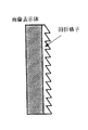
ブレーズド型回折格子とは、図3に示すように、鋸刃状の断面形状を持つ回折格子であり、その斜面での入射光の反射もしくは屈折の角度が、回折角度と一致した場合、非常に高い回折効率が得られることが知られている。
【0027】
バイナリー型回折格子とは、図4に示すように、階段状の断面形状を持つ回折格子であり、この回折格子も非常に高い回折効率を示すことが知られている。
【0028】
上記の回折格子の格子ピッチは、0.1〜20μm程度と非常に細かいため、投影型表示装置の表示面に適用した場合、プリズムシートやフレネルレンズに見られるような、表示画素と単位レンズのピッチの関係に起因するモアレの問題は生じない。
【0029】
上述したように、図2は、光学シートの中央部と周辺部とで回折格子(周期および/または方向)を変化させることにより、特定範囲の観察領域にのみ表示光を効率良く到達させることを示す説明図であり、前記観察領域に表示光を集めるために、周辺部の回折格子のピッチを細かくした場合に係る説明図である。
【0030】
回折格子は、波長によって回折角度が異なる(波長分散)ため、白色に近い光が必要な際には、回折格子の周期を比較的狭い領域内で変化させることで実現される。すなわち、波長の異なる回折光を混合することで、波長分散による影響が回避され、白色に近い回折光が得られることになる。
【0031】
上記の狭い領域の設定にあたっては、軸外し(照明光の中心光軸が、表示光の中心光軸とはずれる場合)で照明光を照射する場合には、0.1〜5μmの範囲より小さい範囲で変化させれば良く、同軸(照明光の中心光軸が、表示光の中心光軸と同じ場合)で照明光を照射する場合には、2〜20μmの範囲より小さい範囲で変化させれば良い。
【0032】
液晶やCRTのように、画素を構成単位とする表示装置では、その画素に対応したセル構造を持つ回折格子からなる光学シートを用いれば、画素から発する光を効率良く表示光に利用することができる。
【0033】
特に、画素毎に対応してR・G・Bの3原色が決まったフルカラー表示を行なう表示装置では、その画素に対応したピッチの回折格子セルからなる光学シートを用いることにより、明るいフルカラー表示が可能となる。
【0034】
また、フルカラー表示の場合、画素:回折格子セルが1:1に対応していなくても、R・G・Bの3画素で1組の集まりに対して1つの回折格子セルを対応させることで、回折格子の波長分散を利用したフルカラー表示も可能である。
【0035】
画像表示面に、回折格子からなる光学シートを配置して、画像表示装置とする場合は、図5〜図7に示す形態が挙げられる。
尚、図5〜図7は、ブレーズド型回折格子に係る説明図であるが、バイナリー型についても同様である。
【0036】
何れの形態でも、表示装置に対して、図の右側から観察することになる。
図5は、回折格子のレリーフ面が表面に露出する使用形態であり、回折格子と空気層との屈折率差が大きいと、回折効果が高くなるという利点がある。
【0037】
図6は、回折格子のレリーフ面に、アルミや銀などの金属反射層や誘電体などを、蒸着・スパッタリングなどにより形成した光学シートを用いた使用形態であり、光学シートは、観察者に対して表示装置の背面に位置する。
【0038】
図7は、回折格子のレリーフ面が表面に露出しない使用形態であり、光学シートは、接着剤により表示装置に接合される。接着剤の屈折率が回折格子と違わなければ、レリーフが埋められて回折格子による機能を奏することがなく、接着剤の屈折率には選定を要する。
同図の構成では、レリーフ面が表面に露出しないため、光学シート表面の汚れや傷が付きにくい。
【0039】
光学シートの領域毎に回折格子の設計を変更することにより、図2で説明した以外にも、例えば以下のことが実現される。
(1)シートに達した光を拡散させるには、図8に示すように、格子の周期をランダムに変化させる。(図8参照)
(2)所定領域のみに表示光を集光させる。図9は、集光範囲が四角形であり、図10は、四角形の集光範囲が2箇所となる状態を概念的に示す説明図である。
【0040】
ブレーズド型またはバイナリー型の回折格子は、以下のように作製される。
まず、目的とする光学機能を実現するような回折格子の形状を設計する。
設計された回折格子の形状となるように、感光材料上で電子線を走査する。
電子線の照射量(強度×走査時間または走査速度)に応じて、回折格子の深さ方向を制御することができる。
【0041】
感光材料を現像して原版を得た後、前記原版を基に、メッキなどにより原版のレリーフ形状が再現されたスタンパ(複製用版)を得ることで、回折格子が大量複製される。
【0042】
【発明の効果】
本発明によって、回折効率が高く充分な光学機能(および、耐久性)を奏する光学シートが、低コストで提供される。
また、光学シートの領域毎に回折格子の形状,ピッチ,深さなどを変化させることにより、領域毎に光学機能を変化させることが可能であるため、1枚の光学シートに複数の機能を持たせることができ、光学部材数の低減も実現でき、表示装置としての一層のコストダウンも図れる。
【0043】
【図面の簡単な説明】
【図1】光学特性が全面に渡って均一な、従来の光学シート(光拡散シート)の光学特性を示す説明図。
【図2】光学シートの中央部と周辺部とで回折格子(周期および/または方向)を変化させることにより、特定範囲の観察領域にのみ表示光を効率良く到達させるようにした、本発明の光学シートの光学特性を示す説明図。
【図3】ブレーズド型回折格子の断面形状を示す説明図。
【図4】バイナリー型回折格子の断面形状を示す説明図。
【図5】画像表示面に、本発明の光学シートを配置する一形態を示す説明図。
【図6】画像表示面に、本発明の光学シートを配置する一形態を示す説明図。
【図7】画像表示面に、本発明の光学シートを配置する一形態を示す説明図。
【図8】断面形状を変化させて、光学特性を変化させる場合に係る光学シートの変形例を示す説明図。
【図9】表示光の集光範囲を変えるように、光学特性を変化させる場合に係る光学シートの変形例を示す説明図。
【図10】表示光の集光範囲を変えるように、光学特性を変化させる場合に係る光学シートの変形例を示す説明図。[0001]
[Technical field to which the invention belongs]
The present invention is an optical that is suitable for improving image quality by increasing brightness, contrast, viewing area, and the like when applied to various image display devices represented by liquid crystal display devices, plasma displays, CRT displays, and the like. Regarding the sheet.
[0002]
[Prior art]
As the optical sheet, those exemplified below are known.
[0003]
(1) The illumination light from the back side of the liquid crystal panel is uniformly irradiated on the entire surface of the liquid crystal panel by an illumination device such as a backlight or an edge light for a liquid crystal display device that requires an illumination device such as a backlight, In order to control the direction, a diffusion sheet, a prism sheet, or the like is used.
[0004]
(2) In order to make the viewing area of an observer for a reflective liquid crystal display device that does not require an illumination device such as a backlight to a certain extent, it is necessary to scatter the reflected light as display light. A diffusion sheet is disposed on the (observer side).
As the diffusion sheet, it is desirable not to diffuse the incident light to the apparatus but to diffuse the light reflected and emitted as display light to the viewer side.
[0005]
In addition to the liquid crystal display devices of the above (1) and (2), any type of display device prevents the reflected light caused by reflection on the surface of the device from being viewed by an observer, so that an antireflection sheet (AR sheet) or antiglare Sheets are also used.
[0006]
[Problems to be solved by the invention]
However, most of the optical sheets described above are intended to perform each function uniformly over the entire surface of the sheet, and it is difficult to change the function (degree) for each region of the sheet.
[0007]
As the display (image display device) has a larger screen, there is a case where a change in characteristics of the optical function according to the position of the screen is required.
For example, in the case of light diffusion, the center of the screen needs to have a diffusibility that spreads symmetrically about an axis perpendicular to the screen, and the right (left) end of the screen is centered on the axis tilted to the left (right). This diffusivity is desirable for an observer located in front of the display.
[0008]
In order to change the characteristics of the optical function for each region of the optical sheet (or to have a plurality of optical functions), it is conceivable to use a hologram. This is because in the hologram, it is easy to change the diffraction characteristics for each region in accordance with the imaging conditions.
[0009]
However, in the case of a volume hologram, since the hologram itself is a photosensitive material, the cost is high and there is a problem in durability.
In the case of a relief hologram, the diffraction efficiency is at most about 20%, and a sufficient optical function as an optical sheet cannot be achieved.
[0010]
An object of the present invention is to provide an optical sheet having a sufficient optical function (and durability) at low cost.
[0011]
[Means for Solving the Problems]
The present invention has been made to solve the above problems,
An optical sheet with improved diffraction efficiency is adopted by forming a blazed or binary diffraction grating on the substrate surface. At that time, the optical grating is not made uniform over the entire surface of the optical sheet, but the optical characteristics of the diffraction grating are changed for each region of the optical sheet.
[0012]
That is, the invention of claim 1
In the optical sheet comprising a blazed diffraction grating on the surface of the translucent sheet,
An optical sheet used for an image display device, characterized in that the direction of a blazed diffraction grating is different between a central portion and a peripheral portion.
[0013]
The invention of claim 2
In the optical sheet in which the surface of the translucent sheet forms a binary diffraction grating whose depth changes stepwise,
At least one of the grating period of the binary diffraction grating, the degree of change of the grating depth, and the direction of the grating is different between the central part and the peripheral part.
[0014]
The invention of claim 3
The grating period of the diffraction grating is characterized in that it has a wide distribution in the central part in the vertical direction and / or the horizontal direction and a narrow distribution in the peripheral part.
[0015]
The invention of claim 4
A light reflecting layer is formed on the surface of the diffraction grating by vapor deposition or sputtering.
[0016]
The invention of claim 5
The cell-like diffraction grating is arranged on the surface of the sheet.
[0017]
The invention of claim 6
It is an image display apparatus of the structure formed by arrange | positioning the optical sheet in any one of Claims 1-5 on an image display surface.
[0018]
The invention of claim 7
An image display device having a configuration in which an optical sheet according to claim 5 is arranged in correspondence with a cell-like diffraction grating and the pixel on an image display surface for displaying an image in pixel units.
[0019]
<Action>
Employing an optical sheet on which a blazed or binary diffraction grating is formed makes it possible to easily emboss the surface of a thermoplastic resin that is less expensive than a photosensitive material. An optical sheet having higher diffraction efficiency and higher optical function can be obtained.
In addition, the diffraction grating is not uniform over the entire surface, and the diffraction grating can be changed for each region of the optical sheet, so that it is easy to design so as to exhibit desired optical characteristics for each region.
[0020]
For example, when an optical sheet is used for light diffusion, if the optical characteristics are uniform over the entire surface of the sheet, as shown in FIG. Diffuse light cannot reach only the observation region.
However, as shown in FIG. 2, by changing the diffraction grating (period and / or direction) between the central part and the peripheral part of the optical sheet, as shown in FIG. Can be achieved efficiently. In order to collect light near the center, it is effective to make the pitch of the diffraction grating in the peripheral part fine.
[0021]
In particular, when the optical sheet is applied to a projector screen, the image quality is improved because the pitch is fine compared to conventional microlenses and Fresnel lenses. In addition, the image quality can be improved in terms of light transmittance and noise.
[0022]
Moreover, by forming a light reflecting layer on the surface of the diffraction grating of the optical sheet by vapor deposition / sputtering, etc., it can be used as a “reflective” optical sheet, and does not require a special illumination light source. Image display by ambient light such as light becomes possible, and display power is saved.
In addition, an adhesive layer can be applied to the surface of the diffraction grating via the light reflecting layer, facilitating device formation. (Claim 4)
[0023]
By disposing an optical sheet having a blazed (or binary) diffraction grating cell as a structural unit on an image display surface that displays an image in pixel units, the cell-like diffraction grating and the pixels are associated with each other, Light from the pixel can be functioned efficiently. (Claims 5 and 7)
In particular, in the case of a liquid crystal display device, the influence of a black matrix, which is a non-pixel around the liquid crystal cell, can be avoided, and display image quality can be improved.
[0024]
As described above, the cost can be reduced by forming the optical sheet using a thermoplastic resin sheet. However, in embossing the thermoplastic resin sheet, a fine diffraction grating is formed with high accuracy. However, it is preferable to use a photosensitive resin (photo-curing resin) for forming a fine diffraction grating with high accuracy.
[0025]
DETAILED DESCRIPTION OF THE INVENTION
Hereinafter, embodiments of the present invention will be described with reference to the drawings.
The diffraction grating of the present invention has a cross-sectional shape different from a relief hologram having a grating having a random cross-sectional shape close to a sine wave shape.
[0026]
As shown in FIG. 3, a blazed diffraction grating is a diffraction grating having a saw-tooth cross-sectional shape. When the angle of reflection or refraction of incident light on the inclined surface coincides with the diffraction angle, It is known that high diffraction efficiency can be obtained.
[0027]
As shown in FIG. 4, the binary diffraction grating is a diffraction grating having a step-like cross-sectional shape, and this diffraction grating is also known to exhibit very high diffraction efficiency.
[0028]
Since the grating pitch of the diffraction grating is as very small as about 0.1 to 20 μm, when applied to the display surface of a projection display device, the display pixels and unit lenses, which are found in prism sheets and Fresnel lenses, are used. The moire problem caused by the pitch relationship does not occur.
[0029]
As described above, FIG. 2 shows that the display light can efficiently reach only the observation region in a specific range by changing the diffraction grating (period and / or direction) between the central portion and the peripheral portion of the optical sheet. It is explanatory drawing shown, and is explanatory drawing which concerns on the case where the pitch of the diffraction grating of a peripheral part is made fine in order to collect display light in the said observation area | region.
[0030]
Since the diffraction grating has a diffraction angle different depending on the wavelength (wavelength dispersion), when light close to white is required, it is realized by changing the period of the diffraction grating within a relatively narrow region. That is, by mixing diffracted light having different wavelengths, the influence of wavelength dispersion is avoided and diffracted light close to white is obtained.
[0031]
In setting the narrow area, when the illumination light is irradiated off-axis (when the central optical axis of the illumination light deviates from the central optical axis of the display light), the range is smaller than the range of 0.1 to 5 μm. If the illumination light is irradiated on the same axis (when the central optical axis of the illumination light is the same as the central optical axis of the display light), it may be changed in a range smaller than the range of 2 to 20 μm. good.
[0032]
As the liquid crystal, a CRT, or a display device as a constituent unit pixel, by using the optical sheet composed of a diffraction grating having a cell structure corresponding to the pixel, be utilized light emanating from pixel to efficiently display light it can.
[0033]
In particular, in a display device that performs full-color display in which the three primary colors R, G, and B are determined corresponding to each pixel, a bright full-color display can be achieved by using an optical sheet composed of diffraction grating cells having a pitch corresponding to the pixel. It becomes possible.
[0034]
In the case of full-color display, even if the pixel: diffraction grating cell does not correspond to 1: 1, one diffraction grating cell is made to correspond to a set of three pixels of R, G, and B. Also, full-color display using the wavelength dispersion of the diffraction grating is possible.
[0035]
In the case where an optical sheet made of a diffraction grating is disposed on the image display surface to form an image display device, the forms shown in FIGS.
5 to 7 are explanatory diagrams relating to the blazed diffraction grating, the same applies to the binary type.
[0036]
In any form, the display device is observed from the right side of the figure.
FIG. 5 shows a usage pattern in which the relief surface of the diffraction grating is exposed on the surface. If the refractive index difference between the diffraction grating and the air layer is large, there is an advantage that the diffraction effect is enhanced.
[0037]
FIG. 6 shows a usage form using an optical sheet in which a metal reflective layer such as aluminum or silver or a dielectric is formed on the relief surface of the diffraction grating by vapor deposition / sputtering, etc. Located on the back of the display.
[0038]
FIG. 7 shows a usage pattern in which the relief surface of the diffraction grating is not exposed on the surface, and the optical sheet is bonded to the display device by an adhesive. If the refractive index of the adhesive is not different from that of the diffraction grating, the relief is buried and the function of the diffraction grating is not exhibited, and the refractive index of the adhesive needs to be selected.
In the configuration shown in the figure, since the relief surface is not exposed on the surface, the surface of the optical sheet is hardly stained or scratched.
[0039]
By changing the design of the diffraction grating for each region of the optical sheet, for example, the following can be realized in addition to that described with reference to FIG.
(1) To diffuse the light that reaches the sheet, the period of the grating is randomly changed as shown in FIG. (See Figure 8)
(2) Condensing display light only in a predetermined area. FIG. 9 is an explanatory diagram conceptually showing a state where the light collection range is a quadrangle, and FIG. 10 is a state where the quadrangular light collection range is two places.
[0040]
The blazed or binary type diffraction grating is manufactured as follows.
First, the shape of the diffraction grating that realizes the target optical function is designed.
An electron beam is scanned on the photosensitive material so as to have the shape of the designed diffraction grating.
The depth direction of the diffraction grating can be controlled according to the electron beam irradiation amount (intensity × scanning time or scanning speed).
[0041]
After developing the photosensitive material to obtain the original plate, a large amount of the diffraction grating is replicated by obtaining a stamper (reproduction plate) in which the relief shape of the original plate is reproduced by plating or the like based on the original plate.
[0042]
【The invention's effect】
According to the present invention, an optical sheet having a high diffraction efficiency and a sufficient optical function (and durability) is provided at low cost.
In addition, since the optical function can be changed for each region by changing the shape, pitch, depth, and the like of the diffraction grating for each region of the optical sheet, one optical sheet has a plurality of functions. The number of optical members can be reduced, and the cost of the display device can be further reduced.
[0043]
[Brief description of the drawings]
FIG. 1 is an explanatory diagram showing optical characteristics of a conventional optical sheet (light diffusion sheet) in which the optical characteristics are uniform over the entire surface.
FIG. 2 shows that the display light can efficiently reach only the observation region in a specific range by changing the diffraction grating (period and / or direction) between the central portion and the peripheral portion of the optical sheet. Explanatory drawing which shows the optical characteristic of an optical sheet.
FIG. 3 is an explanatory diagram showing a cross-sectional shape of a blazed diffraction grating.
FIG. 4 is an explanatory diagram showing a cross-sectional shape of a binary diffraction grating.
FIG. 5 is an explanatory view showing an embodiment in which the optical sheet of the present invention is arranged on the image display surface.
FIG. 6 is an explanatory view showing an embodiment in which the optical sheet of the present invention is arranged on the image display surface.
FIG. 7 is an explanatory view showing an embodiment in which the optical sheet of the present invention is arranged on the image display surface.
FIG. 8 is an explanatory diagram showing a modification of the optical sheet according to the case where the optical characteristics are changed by changing the cross-sectional shape.
FIG. 9 is an explanatory view showing a modification of the optical sheet according to the case where the optical characteristics are changed so as to change the light collection range of the display light.
FIG. 10 is an explanatory diagram illustrating a modification of the optical sheet according to the case where the optical characteristics are changed so as to change the light collection range of the display light.
Claims (7)
ブレーズド型回折格子の方向が、中心部と周辺部では異なることを特徴とする画像表示装置に用いられる光学シート。In the optical sheet comprising a blazed diffraction grating on the surface of the translucent sheet,
An optical sheet used in an image display device, characterized in that the direction of a blazed diffraction grating is different between a central portion and a peripheral portion.
バイナリー型回折格子の格子周期,格子の深さの変化する度合い,格子の方向の少なくとも一つが、中心部と周辺部では異なることを特徴とする画像表示装置に用いられる光学シート。In the optical sheet comprising a binary diffraction grating whose depth changes stepwise on the surface of the translucent sheet,
An optical sheet for use in an image display device, wherein at least one of a grating period of a binary diffraction grating, a degree of change in grating depth, and a grating direction is different between a central part and a peripheral part.
Priority Applications (1)
| Application Number | Priority Date | Filing Date | Title |
|---|---|---|---|
| JP13509898A JP3675170B2 (en) | 1998-05-18 | 1998-05-18 | Optical sheet and image display device using the same |
Applications Claiming Priority (1)
| Application Number | Priority Date | Filing Date | Title |
|---|---|---|---|
| JP13509898A JP3675170B2 (en) | 1998-05-18 | 1998-05-18 | Optical sheet and image display device using the same |
Publications (2)
| Publication Number | Publication Date |
|---|---|
| JPH11326618A JPH11326618A (en) | 1999-11-26 |
| JP3675170B2 true JP3675170B2 (en) | 2005-07-27 |
Family
ID=15143799
Family Applications (1)
| Application Number | Title | Priority Date | Filing Date |
|---|---|---|---|
| JP13509898A Expired - Fee Related JP3675170B2 (en) | 1998-05-18 | 1998-05-18 | Optical sheet and image display device using the same |
Country Status (1)
| Country | Link |
|---|---|
| JP (1) | JP3675170B2 (en) |
Families Citing this family (6)
| Publication number | Priority date | Publication date | Assignee | Title |
|---|---|---|---|---|
| JP4830188B2 (en) | 2000-08-31 | 2011-12-07 | 凸版印刷株式会社 | Light diffuser and display device using the same |
| US7164224B2 (en) | 2000-12-14 | 2007-01-16 | Sharp Kabushiki Kaisha | Backlight having discharge tube, reflector and heat conduction member contacting discharge tube |
| JP4352741B2 (en) * | 2003-03-31 | 2009-10-28 | 凸版印刷株式会社 | Image display body having diffraction grating pattern |
| JP2008083599A (en) * | 2006-09-28 | 2008-04-10 | Toppan Printing Co Ltd | Optical element and display body using the same |
| JP4968234B2 (en) * | 2008-10-21 | 2012-07-04 | セイコーエプソン株式会社 | Optical element and display device |
| AU2011100725B4 (en) * | 2011-06-17 | 2011-09-22 | Innovia Security Pty Ltd | Diffraction grating |
-
1998
- 1998-05-18 JP JP13509898A patent/JP3675170B2/en not_active Expired - Fee Related
Also Published As
| Publication number | Publication date |
|---|---|
| JPH11326618A (en) | 1999-11-26 |
Similar Documents
| Publication | Publication Date | Title |
|---|---|---|
| JP3649145B2 (en) | REFLECTIVE DISPLAY DEVICE, ITS MANUFACTURING METHOD, AND DEVICE USING THE SAME | |
| KR100854223B1 (en) | Optical sheet, rear projection display and liquid crystal display | |
| JP3587852B2 (en) | Backlight assembly for electro-optic display | |
| KR100352732B1 (en) | Rear projection screen | |
| EP0640850A2 (en) | Microlens array sheet for a liquid crystal display, method for attaching the same and liquid crystal display equipped with the same | |
| JP2002107519A (en) | Reflection type display unit, retroreflector | |
| JP3933053B2 (en) | Screen, optical film, and optical film manufacturing method | |
| KR100893903B1 (en) | Optical sheet using a diffraction grating, and display device using the optical sheet | |
| US7703972B2 (en) | Back light unit | |
| JPH10301110A (en) | Picture display device | |
| JP3675170B2 (en) | Optical sheet and image display device using the same | |
| JP2000039515A (en) | Light diffusing plate and liquid crystal display device using it | |
| JPH11202112A (en) | Diffraction optical element | |
| JP2010002913A (en) | Passive matrix liquid crystal display | |
| JPH09120060A (en) | Display device with back light illumination system that supplies collimated light | |
| JP2003021726A (en) | Light guide body and surface light source device and liquid crystal display device both usnig the body | |
| JP2001116908A (en) | Optical sheet and display using same | |
| JP3713993B2 (en) | Reflective liquid crystal display | |
| JP4270412B2 (en) | Light diffusing element composite and image display system using the same | |
| JPH10253801A (en) | Optical element, liquid crystal display unit and liquid crystal projector | |
| JP3669637B2 (en) | Liquid crystal projection display device using hologram color filter | |
| JPH11305677A (en) | Reflection type liquid crystal display device | |
| JP4232918B2 (en) | Diffuse reflection type holographic optical member | |
| JP2000221309A (en) | Light diffuser and liquid crystal display device using the same | |
| JP2001124906A (en) | Off-axis anisotropic light-scattering film and display device using the same |
Legal Events
| Date | Code | Title | Description |
|---|---|---|---|
| A131 | Notification of reasons for refusal |
Free format text: JAPANESE INTERMEDIATE CODE: A131 Effective date: 20040210 |
|
| A521 | Written amendment |
Free format text: JAPANESE INTERMEDIATE CODE: A523 Effective date: 20040412 |
|
| TRDD | Decision of grant or rejection written | ||
| A01 | Written decision to grant a patent or to grant a registration (utility model) |
Free format text: JAPANESE INTERMEDIATE CODE: A01 Effective date: 20050412 |
|
| A61 | First payment of annual fees (during grant procedure) |
Free format text: JAPANESE INTERMEDIATE CODE: A61 Effective date: 20050425 |
|
| R150 | Certificate of patent (=grant) or registration of utility model |
Free format text: JAPANESE INTERMEDIATE CODE: R150 |
|
| FPAY | Renewal fee payment (prs date is renewal date of database) |
Free format text: PAYMENT UNTIL: 20080513 Year of fee payment: 3 |
|
| FPAY | Renewal fee payment (prs date is renewal date of database) |
Free format text: PAYMENT UNTIL: 20090513 Year of fee payment: 4 |
|
| FPAY | Renewal fee payment (prs date is renewal date of database) |
Free format text: PAYMENT UNTIL: 20100513 Year of fee payment: 5 |
|
| FPAY | Renewal fee payment (prs date is renewal date of database) |
Free format text: PAYMENT UNTIL: 20110513 Year of fee payment: 6 |
|
| FPAY | Renewal fee payment (prs date is renewal date of database) |
Free format text: PAYMENT UNTIL: 20110513 Year of fee payment: 6 |
|
| FPAY | Renewal fee payment (prs date is renewal date of database) |
Free format text: PAYMENT UNTIL: 20120513 Year of fee payment: 7 |
|
| FPAY | Renewal fee payment (prs date is renewal date of database) |
Free format text: PAYMENT UNTIL: 20120513 Year of fee payment: 7 |
|
| FPAY | Renewal fee payment (prs date is renewal date of database) |
Free format text: PAYMENT UNTIL: 20130513 Year of fee payment: 8 |
|
| FPAY | Renewal fee payment (prs date is renewal date of database) |
Free format text: PAYMENT UNTIL: 20140513 Year of fee payment: 9 |
|
| LAPS | Cancellation because of no payment of annual fees |