JP3616514B2 - Semiconductor integrated circuit and manufacturing method thereof - Google Patents
Semiconductor integrated circuit and manufacturing method thereof Download PDFInfo
- Publication number
- JP3616514B2 JP3616514B2 JP32697398A JP32697398A JP3616514B2 JP 3616514 B2 JP3616514 B2 JP 3616514B2 JP 32697398 A JP32697398 A JP 32697398A JP 32697398 A JP32697398 A JP 32697398A JP 3616514 B2 JP3616514 B2 JP 3616514B2
- Authority
- JP
- Japan
- Prior art keywords
- electrode
- region
- gate
- gate electrode
- integrated circuit
- Prior art date
- Legal status (The legal status is an assumption and is not a legal conclusion. Google has not performed a legal analysis and makes no representation as to the accuracy of the status listed.)
- Expired - Fee Related
Links
- 239000004065 semiconductor Substances 0.000 title claims description 331
- 238000004519 manufacturing process Methods 0.000 title claims description 93
- 229910021332 silicide Inorganic materials 0.000 claims description 209
- FVBUAEGBCNSCDD-UHFFFAOYSA-N silicide(4-) Chemical compound [Si-4] FVBUAEGBCNSCDD-UHFFFAOYSA-N 0.000 claims description 209
- 239000012535 impurity Substances 0.000 claims description 174
- 238000000034 method Methods 0.000 claims description 82
- 239000000203 mixture Substances 0.000 claims description 67
- 239000000758 substrate Substances 0.000 claims description 48
- 230000008569 process Effects 0.000 claims description 42
- 229910019001 CoSi Inorganic materials 0.000 claims description 24
- 230000005669 field effect Effects 0.000 claims description 15
- 229910052710 silicon Inorganic materials 0.000 claims description 13
- 150000001875 compounds Chemical class 0.000 claims description 7
- 229910008484 TiSi Inorganic materials 0.000 claims description 6
- 230000003247 decreasing effect Effects 0.000 claims description 5
- 238000009413 insulation Methods 0.000 claims description 4
- 229910052751 metal Inorganic materials 0.000 claims description 4
- 239000002184 metal Substances 0.000 claims description 4
- 230000015572 biosynthetic process Effects 0.000 description 94
- 229910021480 group 4 element Inorganic materials 0.000 description 80
- 239000010410 layer Substances 0.000 description 75
- 239000007789 gas Substances 0.000 description 60
- 238000009792 diffusion process Methods 0.000 description 47
- 230000000295 complement effect Effects 0.000 description 40
- 229910000577 Silicon-germanium Inorganic materials 0.000 description 39
- 230000000694 effects Effects 0.000 description 29
- 238000005468 ion implantation Methods 0.000 description 28
- 230000009977 dual effect Effects 0.000 description 26
- 238000000137 annealing Methods 0.000 description 23
- 238000002513 implantation Methods 0.000 description 23
- 238000002955 isolation Methods 0.000 description 23
- 239000011229 interlayer Substances 0.000 description 19
- 238000010586 diagram Methods 0.000 description 17
- 238000005229 chemical vapour deposition Methods 0.000 description 14
- 238000009826 distribution Methods 0.000 description 13
- ATJFFYVFTNAWJD-UHFFFAOYSA-N Tin Chemical compound [Sn] ATJFFYVFTNAWJD-UHFFFAOYSA-N 0.000 description 11
- 238000004544 sputter deposition Methods 0.000 description 11
- 230000010354 integration Effects 0.000 description 10
- 239000012528 membrane Substances 0.000 description 10
- 229910021421 monocrystalline silicon Inorganic materials 0.000 description 9
- 230000007423 decrease Effects 0.000 description 8
- 150000002500 ions Chemical class 0.000 description 8
- 230000004913 activation Effects 0.000 description 7
- 238000005530 etching Methods 0.000 description 7
- 238000000206 photolithography Methods 0.000 description 7
- 238000004151 rapid thermal annealing Methods 0.000 description 7
- QAOWNCQODCNURD-UHFFFAOYSA-N Sulfuric acid Chemical compound OS(O)(=O)=O QAOWNCQODCNURD-UHFFFAOYSA-N 0.000 description 6
- 230000003647 oxidation Effects 0.000 description 6
- 238000007254 oxidation reaction Methods 0.000 description 6
- 230000001590 oxidative effect Effects 0.000 description 6
- 230000004888 barrier function Effects 0.000 description 5
- 239000002131 composite material Substances 0.000 description 5
- 238000001451 molecular beam epitaxy Methods 0.000 description 5
- 230000035515 penetration Effects 0.000 description 5
- 229910004298 SiO 2 Inorganic materials 0.000 description 4
- 238000000151 deposition Methods 0.000 description 4
- 230000008021 deposition Effects 0.000 description 4
- 238000005498 polishing Methods 0.000 description 4
- MHAJPDPJQMAIIY-UHFFFAOYSA-N Hydrogen peroxide Chemical compound OO MHAJPDPJQMAIIY-UHFFFAOYSA-N 0.000 description 3
- 230000008859 change Effects 0.000 description 3
- 150000001793 charged compounds Chemical class 0.000 description 3
- 239000002019 doping agent Substances 0.000 description 3
- 239000011259 mixed solution Substances 0.000 description 3
- 238000011084 recovery Methods 0.000 description 3
- 230000009467 reduction Effects 0.000 description 3
- 238000009751 slip forming Methods 0.000 description 3
- 239000000126 substance Substances 0.000 description 3
- 229910016570 AlCu Inorganic materials 0.000 description 2
- NBIIXXVUZAFLBC-UHFFFAOYSA-N Phosphoric acid Chemical compound OP(O)(O)=O NBIIXXVUZAFLBC-UHFFFAOYSA-N 0.000 description 2
- VYPSYNLAJGMNEJ-UHFFFAOYSA-N Silicium dioxide Chemical compound O=[Si]=O VYPSYNLAJGMNEJ-UHFFFAOYSA-N 0.000 description 2
- BOTDANWDWHJENH-UHFFFAOYSA-N Tetraethyl orthosilicate Chemical compound CCO[Si](OCC)(OCC)OCC BOTDANWDWHJENH-UHFFFAOYSA-N 0.000 description 2
- 239000005380 borophosphosilicate glass Substances 0.000 description 2
- 239000004020 conductor Substances 0.000 description 2
- 238000011109 contamination Methods 0.000 description 2
- 239000013078 crystal Substances 0.000 description 2
- 239000012212 insulator Substances 0.000 description 2
- 238000010030 laminating Methods 0.000 description 2
- 150000004767 nitrides Chemical class 0.000 description 2
- 238000000059 patterning Methods 0.000 description 2
- 229910021420 polycrystalline silicon Inorganic materials 0.000 description 2
- 238000005204 segregation Methods 0.000 description 2
- 229910015900 BF3 Inorganic materials 0.000 description 1
- ZOXJGFHDIHLPTG-UHFFFAOYSA-N Boron Chemical compound [B] ZOXJGFHDIHLPTG-UHFFFAOYSA-N 0.000 description 1
- PXGOKWXKJXAPGV-UHFFFAOYSA-N Fluorine Chemical compound FF PXGOKWXKJXAPGV-UHFFFAOYSA-N 0.000 description 1
- 229910003811 SiGeC Inorganic materials 0.000 description 1
- BLRPTPMANUNPDV-UHFFFAOYSA-N Silane Chemical compound [SiH4] BLRPTPMANUNPDV-UHFFFAOYSA-N 0.000 description 1
- XUIMIQQOPSSXEZ-UHFFFAOYSA-N Silicon Chemical compound [Si] XUIMIQQOPSSXEZ-UHFFFAOYSA-N 0.000 description 1
- 229910000147 aluminium phosphate Inorganic materials 0.000 description 1
- 229910052785 arsenic Inorganic materials 0.000 description 1
- RQNWIZPPADIBDY-UHFFFAOYSA-N arsenic atom Chemical compound [As] RQNWIZPPADIBDY-UHFFFAOYSA-N 0.000 description 1
- 229910052796 boron Inorganic materials 0.000 description 1
- WTEOIRVLGSZEPR-UHFFFAOYSA-N boron trifluoride Chemical compound FB(F)F WTEOIRVLGSZEPR-UHFFFAOYSA-N 0.000 description 1
- 230000015556 catabolic process Effects 0.000 description 1
- 229910052681 coesite Inorganic materials 0.000 description 1
- 229910052906 cristobalite Inorganic materials 0.000 description 1
- 238000006731 degradation reaction Methods 0.000 description 1
- 230000000593 degrading effect Effects 0.000 description 1
- 238000000407 epitaxy Methods 0.000 description 1
- 229910052731 fluorine Inorganic materials 0.000 description 1
- 239000011737 fluorine Substances 0.000 description 1
- 229910000078 germane Inorganic materials 0.000 description 1
- 238000007373 indentation Methods 0.000 description 1
- 238000004518 low pressure chemical vapour deposition Methods 0.000 description 1
- 239000000463 material Substances 0.000 description 1
- 229910044991 metal oxide Inorganic materials 0.000 description 1
- 150000004706 metal oxides Chemical class 0.000 description 1
- 238000005268 plasma chemical vapour deposition Methods 0.000 description 1
- 238000012827 research and development Methods 0.000 description 1
- 229910000077 silane Inorganic materials 0.000 description 1
- 239000010703 silicon Substances 0.000 description 1
- 239000000377 silicon dioxide Substances 0.000 description 1
- 235000012239 silicon dioxide Nutrition 0.000 description 1
- 239000007787 solid Substances 0.000 description 1
- 229910052682 stishovite Inorganic materials 0.000 description 1
- 230000007704 transition Effects 0.000 description 1
- 229910052905 tridymite Inorganic materials 0.000 description 1
Images


Classifications
-
- H—ELECTRICITY
- H01—ELECTRIC ELEMENTS
- H01L—SEMICONDUCTOR DEVICES NOT COVERED BY CLASS H10
- H01L21/00—Processes or apparatus adapted for the manufacture or treatment of semiconductor or solid state devices or of parts thereof
- H01L21/02—Manufacture or treatment of semiconductor devices or of parts thereof
- H01L21/04—Manufacture or treatment of semiconductor devices or of parts thereof the devices having potential barriers, e.g. a PN junction, depletion layer or carrier concentration layer
- H01L21/18—Manufacture or treatment of semiconductor devices or of parts thereof the devices having potential barriers, e.g. a PN junction, depletion layer or carrier concentration layer the devices having semiconductor bodies comprising elements of Group IV of the Periodic Table or AIIIBV compounds with or without impurities, e.g. doping materials
- H01L21/28—Manufacture of electrodes on semiconductor bodies using processes or apparatus not provided for in groups H01L21/20 - H01L21/268
- H01L21/28008—Making conductor-insulator-semiconductor electrodes
- H01L21/28017—Making conductor-insulator-semiconductor electrodes the insulator being formed after the semiconductor body, the semiconductor being silicon
- H01L21/28026—Making conductor-insulator-semiconductor electrodes the insulator being formed after the semiconductor body, the semiconductor being silicon characterised by the conductor
- H01L21/2807—Making conductor-insulator-semiconductor electrodes the insulator being formed after the semiconductor body, the semiconductor being silicon characterised by the conductor the final conductor layer next to the insulator being Si or Ge or C and their alloys except Si
-
- H—ELECTRICITY
- H10—SEMICONDUCTOR DEVICES; ELECTRIC SOLID-STATE DEVICES NOT OTHERWISE PROVIDED FOR
- H10D—INORGANIC ELECTRIC SEMICONDUCTOR DEVICES
- H10D30/00—Field-effect transistors [FET]
- H10D30/80—FETs having rectifying junction gate electrodes
- H10D30/801—FETs having heterojunction gate electrodes
-
- H—ELECTRICITY
- H10—SEMICONDUCTOR DEVICES; ELECTRIC SOLID-STATE DEVICES NOT OTHERWISE PROVIDED FOR
- H10D—INORGANIC ELECTRIC SEMICONDUCTOR DEVICES
- H10D84/00—Integrated devices formed in or on semiconductor substrates that comprise only semiconducting layers, e.g. on Si wafers or on GaAs-on-Si wafers
- H10D84/01—Manufacture or treatment
- H10D84/0123—Integrating together multiple components covered by H10D12/00 or H10D30/00, e.g. integrating multiple IGBTs
- H10D84/0126—Integrating together multiple components covered by H10D12/00 or H10D30/00, e.g. integrating multiple IGBTs the components including insulated gates, e.g. IGFETs
- H10D84/0165—Integrating together multiple components covered by H10D12/00 or H10D30/00, e.g. integrating multiple IGBTs the components including insulated gates, e.g. IGFETs the components including complementary IGFETs, e.g. CMOS devices
- H10D84/0172—Manufacturing their gate conductors
- H10D84/0174—Manufacturing their gate conductors the gate conductors being silicided
-
- H—ELECTRICITY
- H10—SEMICONDUCTOR DEVICES; ELECTRIC SOLID-STATE DEVICES NOT OTHERWISE PROVIDED FOR
- H10D—INORGANIC ELECTRIC SEMICONDUCTOR DEVICES
- H10D84/00—Integrated devices formed in or on semiconductor substrates that comprise only semiconducting layers, e.g. on Si wafers or on GaAs-on-Si wafers
- H10D84/01—Manufacture or treatment
- H10D84/0123—Integrating together multiple components covered by H10D12/00 or H10D30/00, e.g. integrating multiple IGBTs
- H10D84/0126—Integrating together multiple components covered by H10D12/00 or H10D30/00, e.g. integrating multiple IGBTs the components including insulated gates, e.g. IGFETs
- H10D84/0165—Integrating together multiple components covered by H10D12/00 or H10D30/00, e.g. integrating multiple IGBTs the components including insulated gates, e.g. IGFETs the components including complementary IGFETs, e.g. CMOS devices
- H10D84/0172—Manufacturing their gate conductors
- H10D84/0177—Manufacturing their gate conductors the gate conductors having different materials or different implants
-
- H—ELECTRICITY
- H10—SEMICONDUCTOR DEVICES; ELECTRIC SOLID-STATE DEVICES NOT OTHERWISE PROVIDED FOR
- H10D—INORGANIC ELECTRIC SEMICONDUCTOR DEVICES
- H10D84/00—Integrated devices formed in or on semiconductor substrates that comprise only semiconducting layers, e.g. on Si wafers or on GaAs-on-Si wafers
- H10D84/01—Manufacture or treatment
- H10D84/02—Manufacture or treatment characterised by using material-based technologies
- H10D84/03—Manufacture or treatment characterised by using material-based technologies using Group IV technology, e.g. silicon technology or silicon-carbide [SiC] technology
- H10D84/038—Manufacture or treatment characterised by using material-based technologies using Group IV technology, e.g. silicon technology or silicon-carbide [SiC] technology using silicon technology, e.g. SiGe
-
- H—ELECTRICITY
- H01—ELECTRIC ELEMENTS
- H01L—SEMICONDUCTOR DEVICES NOT COVERED BY CLASS H10
- H01L2924/00—Indexing scheme for arrangements or methods for connecting or disconnecting semiconductor or solid-state bodies as covered by H01L24/00
- H01L2924/0001—Technical content checked by a classifier
- H01L2924/0002—Not covered by any one of groups H01L24/00, H01L24/00 and H01L2224/00
Landscapes
- Engineering & Computer Science (AREA)
- Physics & Mathematics (AREA)
- Condensed Matter Physics & Semiconductors (AREA)
- General Physics & Mathematics (AREA)
- Manufacturing & Machinery (AREA)
- Computer Hardware Design (AREA)
- Microelectronics & Electronic Packaging (AREA)
- Power Engineering (AREA)
- Metal-Oxide And Bipolar Metal-Oxide Semiconductor Integrated Circuits (AREA)
- Insulated Gate Type Field-Effect Transistor (AREA)
- Electrodes Of Semiconductors (AREA)
Description
【0001】
【発明の属する技術分野】
本発明は半導体集積回路及びその製造方法に関する。特に本発明は、種類の異なる少なくとも2種類以上の四族元素(IV族元素)の領域を有するゲート電極で絶縁ゲート型電界効果トランジスタを構築した半導体集積回路及びその製造方法に関する。さらに、本発明は、絶縁ゲート型電界効果トランジスタのソース電極又はドレイン電極として使用される主電極にエレベーテッド電極を備えた半導体集積回路及びその製造方法に関する。
【0002】
【従来の技術】
半導体集積回路を構築するMOSFET(Metal Oxide Simeconductor Field Effect Transistor)の微細化に伴い、MOSFETのゲート絶縁膜は薄膜化される傾向にある。さらに、微細化に伴う短チャネル効果を抑制するために、相補型MOSFETにおいてはデュアルゲート(dual gate)電極構造が採用される傾向にある。デュアルゲート電極構造とは、nチャネルMOSFETのゲート電極をn型に設定し、pチャネルMOSFETのゲート電極をp型に設定した構造である。
【0003】
デュアルゲート電極構造は、一般的に通常の相補型MOSFETの製造プロセスを利用し、製造工程数を増加させることなく形成される。すなわち、まず、nチャネルMOSFETにおいては、n型半導体領域のソース電極及びドレイン電極を形成するn型不純物のドーピングと同時に同一のn型不純物がゲート電極にドーピングされる。pチャネルMOSFETにおいては、p型半導体領域のソース電極及びドレイン電極を形成するp型不純物のドーピングと同時に同一のp型不純物がゲート電極にドーピングされる。ドーピングにはイオン注入法が使用される。そして、アニールが行われ、ドーピングされた不純物が拡散されるとともに活性化される。n型不純物がドーピングされたゲート電極はn型に設定され、p型不純物がドーピングされたゲート電極はp型に設定される。
【0004】
さらに、MOSFETの微細化に伴い、MOSFETのソース電極及びドレイン電極のシャロー化並びに低抵抗化が要求されている。このシャロー化並びに低抵抗化にはエレベーテッド(elevated source drain又はraised source drain)電極構造を採用することが最適である。エレベーテッド電極構造は、単結晶Si基板表面部に形成したソース電極(半導体領域)上、ドレイン電極(半導体領域)上のそれぞれにエレベーテッド電極を積み重ねた電極構造である。エレベーテッド電極は単結晶Si基板上に成長させたエピタキシャル成長層で形成され、ソース電極及びドレイン電極はエレベーテッド電極の形成後にエレベーテッド電極を固体拡散源として単結晶Si基板表面部に不純物を拡散することにより形成される。エレベーテッド電極構造においては、ソース電極及びドレイン電極が単結晶Si基板表面からの拡散で形成されるので、浅い接合が形成できる。さらに、エレベーテッド電極構造においては、ソース電極上にエレベーテッド電極が、同様にドレイン電極上にエレベーテッド電極が各々重ね合わされているので、電極の抵抗値を低減させることができる。
【0005】
【発明が解決しようとする課題】
しかしながら、前述のMOSFETを備えた半導体集積回路においては、以下の点について配慮がなされていない。
【0006】
(1)デュアルゲート電極構造の採用によりnチャネルMOSFET、pチャネルMOSFETのそれぞれに個別の問題が発生する。pチャネルMOSFETにおいては、浅い接合のソース電極及びドレイン電極を形成するために、イオン注入にはイオン注入分布を浅くできるBF2(弗化硼素)イオンが使用される。この場合、B(硼素)と同時にイオン注入されるF(弗素)がゲート絶縁膜(ゲート酸化膜)中に侵入し、このFがゲート絶縁膜中のBの拡散を促進させてしまうので、ゲート電極から基板(チャネル形成領域)にBが突き抜けてしまう。微細化に伴うゲート絶縁膜の薄膜化はこのようなBの突き抜けを助長してしまう。仮にFが存在しなくてもゲート絶縁膜の薄膜化によりBの突き抜けが発生する。このため、pチャネルMOSFETの閾値電圧を変動させてしまうので、半導体集積回路の電気的信頼性を低下させてしまうという問題があった。
【0007】
一方、nチャネルMOSFETにおいては、同様に浅い接合のソース電極及びドレイン電極を形成するために、イオン注入には拡散速度が遅いAs(砒素)イオンが使用される。製造工程数の増加を避けるためにはソース電極及びドレイン電極と同様にゲート電極にドーピングされるn型不純物にはAsイオンが使用される。このAsイオンは、浅い接合のソース電極及びドレイン電極を形成するには(ソース電極及びドレイン電極のシャロー化を図るには)適しているが、逆に拡散速度が遅いのでゲート電極全体に高濃度に拡散させることが難しく、ゲート電極のゲート絶縁膜側においてAs濃度が不充分になる。特に、ソース電極及びドレイン電極のシャロー化のためにアニール温度が低温化される傾向にあり、またアニール時間が短時間化される傾向にあり、ゲート電極のゲート絶縁膜側のAs濃度不足はより一層助長されてしまう。このため、実動作でゲート電極にゲートバイアスを印加するとゲート電極内に空乏層が発生し、nチャネルMOSFETの閾値電圧を変動させてしまうので、半導体集積回路の電気的信頼性を低下させてしまうという問題があった。
【0008】
(2)このように、半導体集積回路の電気的信頼性を低下させてしまうので、MOSFETの微細化の障害になり、半導体集積回路の集積化を実現することができないという問題があった。
【0009】
(3)特開平4−25176号公報には、pチャネルMOSFETにおいてBの突き抜けを防止する発明が開示されている。この公報に開示された発明によれば、多結晶SiにGe等の不純物を含むゲート電極を形成し、このゲート電極にBをイオン注入法でドーピングすることにより、熱工程における多結晶Siのグレイン成長を抑制することができ、グレインに沿うBの拡散を抑えることができる。しかしながら、最近のゲート電極には低抵抗化のためにゲート電極上部をシリサイド化したシリサイド電極を形成する傾向にあり、このシリサイド電極にゲート電極のGe等の不純物が含まれるとシリサイド電極の抵抗値が高くなってしまう。このため、MOSFETのスイッチング動作速度の高速化や低電源電圧化が実現できないという問題があった。
【0010】
(4)エレベーテッド電極構造において、特にpチャネルMOSFETのソース電極及びドレイン電極を形成するp型不純物にはBが使用されており、このBは拡散速度がn型不純物としてのAsに比べて速い。このため、pチャネルMOSFETにおいて充分なシャロー化が得られないので、半導体集積回路の集積化を実現することができないという問題があった。
【0011】
(5)エレベーテッド電極構造において、エレベーテッド電極中のBの活性濃度を充分に得ることができないので、エレベーテッド電極の抵抗値が増加してしまう。このため、pチャネルMOSFETのスイッチング動作速度の高速化や低電源電圧化が実現できないという問題があった。
【0012】
(6)エレベーテッド電極構造において、低抵抗化のためにエレベーテッド電極にシリサイド電極を形成する研究開発が進められている。しかしながら、エレベーテッド電極とシリサイド電極との間の接触抵抗値を充分に小さくすることができないので、MOSFETのスイッチング動作速度の高速化や低電源電圧化が実現できないという問題があった。
【0013】
本発明は上記課題を解決するためになされたものである。従って、本発明の第1の目的は、ゲート電極にドーピングされた不純物のチャネル領域側への漏れを防止することにより、安定した閾値電圧を得ることができ、電気的信頼性を向上させることができる絶縁ゲート型電界効果トランジスタ(MISFET:Metal Insulator Semiconductor Field Effect Transistor)を備えた半導体集積回路を提供することである。
本発明の第2の目的は、ゲート電極にドーピングされた不純物の濃度を全域にわたって充分に確保し、ゲート電極の空乏層化を防止することにより、安定した閾値電圧を得ることができ、電気的信頼性を向上させることができるMISFETを備えた半導体集積回路を提供することである。
本発明の第3の目的は、第1の目的並びに第2の目的を同時に達成することができる半導体集積回路を提供することである。特に、本発明の第3の目的は、相補型MISFETのいずれのチャネル導電型のMISFETにおいても安定した閾値電圧を得ることができ、電気的信頼性を向上させることができる半導体集積回路を提供することである。
本発明の第4の目的は、第1乃至第3の目的の少なくともいずれか1つの目的を達成しつつ、MISFETの微細化を図り、集積度を向上させることができる半導体集積回路を提供することである。
本発明の第5の目的は、第1乃至第3の目的の少なくともいずれか1つの目的を達成しつつ、MISFETのスイッチング動作速度の高速化並びに低電源電圧化を実現することができ、回路動作速度の高速化並びに低消費電力化を実現することができる半導体集積回路を提供することである。特に本発明の第5の目的は、MISFETのゲート電極に備えたシリサイド電極の抵抗値を減少させることにより、MISFETのスイッチング動作速度の高速化並びに低電源電圧化を実現することができ、回路動作速度の高速化並びに低消費電力化を実現することができる半導体集積回路を提供することである。
本発明の第6の目的は、第1乃至第5の目的の少なくともいずれか1つの目的を達成しつつ、製造工程数を低減させることができる半導体集積回路の製造方法を提供することである。特に、本発明の第6の目的は、相補型MISFETの製造工程数を低減させることができる半導体集積回路の製造方法を提供することである。
【0014】
本発明の第7の目的は、エレベーテッド電極を備えたMISFETのソース電極及びドレイン電極(主電極)のシャロー化を図り、MISFETの微細化を実現することにより、集積度を向上させることができる半導体集積回路を提供することである。本発明の第8の目的は、第7の目的を達成しつつ、エレベーテッド電極の低抵抗化並びに低電源電圧化を実現し、回路動作速度の高速化並びに低消費電力化を実現することができる半導体集積回路を提供することである。
本発明の第9の目的は、第7又は第8の目的を達成しつつ、エレベーテッド電極とシリサイド電極との接触抵抗値を減少させ、回路動作速度の高速化並びに低消費電力化を実現することができる半導体集積回路を提供することである。
本発明の第10の目的は、第7乃至第9の目的を達成しつつ、製造工程数を低減させることができる半導体集積回路の製造方法を提供することである。
本発明の第11の目的は、第1乃至第10の目的の少なくとも2以上の目的を同時に達成することができる半導体集積回路又は半導体集積回路の製造方法を提供することである。
【0015】
【課題を解決するための手段】
上記課題を解決するために、この発明の第1の特徴は、半導体集積回路において、MISFETのゲート電極のゲート絶縁膜側の第1領域が種類の異なる少なくとも第1四族元素及び第2四族元素で形成され、ゲート電極のゲート絶縁膜から離間された第2領域が第1四族元素で形成されたことである。
ゲート電極の第1領域は第2四族元素の組成比をゲート絶縁膜からの距離に応じて連続的に、又は第2四族元素の組成比をゲート絶縁膜からの距離に応じて段階的に減少させることが好ましい。
ゲート電極の第1四族元素にはSi、第2四族元素にはGe又はCが実用的に使用できる。ゲート電極の第1領域はSiで形成されたゲート電極の場合に発生するゲート空乏層の幅よりも厚く形成されることが好ましい。第1領域のGeの組成比は実用的に少なくとも0.1以上に設定される。ゲート絶縁膜とゲート電極の第1領域との間には第1領域の厚さよりも薄い膜厚例えば1nm以下の膜厚の第1四族元素の層すなわちGeが実質的に含まれないSi層又は第2四族元素の層すなわちSiが実質的に含まれないGe層が存在してもよい。
pチャネルMISFETのゲート電極には少なくともBが含まれる。nチャネルMISFETのゲート電極には少なくともAsが含まれる。
このように構成される半導体集積回路においては、pチャネルMISFETの場合、ゲート電極のゲート絶縁膜側に第2四族元素であるGe又はCが含まれるので、p型不純物であるBの拡散速度を減少させ、Bのチャネル領域側への漏れを防止することができる。従って、pチャネルMISFETの閾値電圧を安定化させることができ、半導体集積回路の電気的信頼性を向上させることができる。さらに、nチャネルMISFETの場合、ゲート電極のゲート絶縁膜側に第2四族元素であるGe又はCが含まれるので、n型不純物であるAsの拡散速度を促進し、ゲート電極全域にわたってAsの不純物濃度を充分に確保することができる。従って、ゲート電極の空乏層化を防止することができ、nチャネルMISFETの閾値電圧を安定化させることができるので、半導体集積回路の電気的信頼性を向上させることができる。特に、デュアルゲート電極構造の相補型MISFETを備えた半導体集積回路においては、第1及び第2四族元素を含む同一ゲート電極の使用でpチャネルMISFET、nチャネルMISFETのそれぞれの閾値電圧を同時に安定化させることができる。この結果、MISFETの微細化を実現することができ、半導体集積回路の集積度を向上させることができる。
【0016】
この発明の第2の特徴は、第1の特徴の半導体集積回路において、MISFETのゲート電極の第2領域に接して形成され、第2四族元素が実質的に含まれないシリサイド電極を備えたことである。シリサイド電極は第2四族元素であるGe又はCが実質的に含まれないシリサイド電極であり、シリサイド電極にはCoSiy層又はTiSiy層が実用的に使用できる。
このように構成される半導体集積回路においては、シリサイド電極に第2四族元素が実質的に含まれないことでシリサイド電極の抵抗値を減少させることができ、MISFETのスイッチング動作速度の高速化並びに低電源電圧化を実現することができる。従って、半導体集積回路の回路動作速度の高速化並びに低消費電力化を実現することができる。
【0017】
この発明の第3の特徴は、MISFETを備えた半導体集積回路において、ゲート電極のゲート絶縁膜側の第1領域が種類の異なる少なくとも第1四族元素及び第2四族元素で形成され、ゲート電極のゲート絶縁膜から離間された第2領域が少なくとも第1四族元素、第2四族元素及び金属を含む多元化合物で形成されたMISFETと、ゲート電極の第2領域に接して形成され、第1四族元素及び金属を含み、第2四族元素が実質的に含まれないシリサイド電極と、を備えたことである。 このように構成される半導体集積回路においては、MISFETのゲート電極の第2領域が多元化合物であってもこの発明の第2の特徴の半導体集積回路と同様の効果が得られる。
【0018】
この発明の第4の特徴は、MISFETを備えた半導体集積回路の製造方法において、下記工程を備えたことである。
(1)種類の異なる少なくとも第1四族元素及び第2四族元素でゲート絶縁膜側に形成された第1領域と、第1四族元素でゲート絶縁膜から離間されて形成された第2領域とを有する、MISFETのゲート電極を形成する工程。
(2)ゲート電極の第2領域の少なくとも一部をシリサイド化してシリサイド電極を形成する工程。
このような半導体集積回路の製造方法においては、第1四族元素で形成された第2領域の範囲内でシリサイド化を行いシリサイド電極を形成したので、シリサイド電極には実質的に第2四族元素(例えばGe又はC)が含まれないシリサイド電極を形成することができる。従って、製造工程数を増加することなく、容易にシリサイド電極の抵抗値を減少させることができる。なお、ゲート電極の第2領域のすべてをシリサイド化し、シリサイド電極が直接ゲート電極の第1領域に接触してもよい。この場合のシリサイド電極は、同様に実質的に第2四族元素を含まない。
【0019】
この発明の第5の特徴は、MISFETを備えた半導体集積回路の製造方法において、下記工程を備えたことである。
(1)種類の異なる少なくとも第1四族元素及び第2四族元素でゲート絶縁膜側に形成された第1領域と、第1四族元素でゲート絶縁膜から離間されて形成された第2領域とを有する、第1チャネル導電型のMISFETの第1ゲート電極、及び第1チャネル導電型とは反対導電型の第2チャネル導電型のMISFETの第2ゲート電極を形成する工程。
(2)第1ゲート電極に第1導電型不純物を導入し、第2ゲート電極に第2導電型不純物を導入する工程。第1ゲート電極に第1導電型不純物を導入する工程は、製造工程数を減少させるために第1チャネル導電型のMISFETにおいてソース電極又はドレイン電極である主電極を形成する第1導電型不純物の導入工程と同一工程であることが好ましい。同様に、第2ゲート電極に第2導電型不純物を導入する工程は第2チャネル導電型のMISFETにおいてソース電極及びドレイン電極である主電極を形成する第2導電型不純物の導入工程と同一工程であることが好ましい。
(3)第1ゲート電極、第2ゲート電極のそれぞれの第2領域の少なくとも一部をシリサイド化してシリサイド電極を形成する工程。
このような半導体集積回路の製造方法においては、第1領域及び第2領域を有するゲート電極を相補型MISFETのそれぞれにおいて同一製造工程で形成し、デュアルゲート電極構造の相補型MISFETを形成することができるので、ゲート電極を相補型MISFETのそれぞれで別々に形成する場合に比べて製造工程数を減少させることができる。さらに、相補型MISFETのそれぞれにおいては、第1の特徴の半導体集積回路で得られる効果並びに第4の特徴の半導体集積回路の製造方法で得られる効果と同一の効果を得ることができる。
【0020】
この発明の第6の特徴は、半導体集積回路において、第1導電型の半導体領域と、半導体領域上の第1領域が種類の異なる少なくとも第1四族元素及び第2四族元素で形成され、半導体領域から離間された第2領域が第1四族元素で形成されたエピタキシャル成長層と、エピタキシャル成長層の第2領域上のシリサイド電極と、を備えたことである。
半導体領域はMISFETのソース電極又はドレイン電極として使用される主電極であり、エピタキシャル成長層はエレベーテッドソース電極又はエレベーテッドドレイン電極として使用されるエレベーテッド電極である。エレベーテッド電極の第1四族元素にはSiが、エレベーテッド電極の第2四族元素にはGe又はCが実用的に使用できる。好ましくは、エレベーテッド電極の第1領域はGeの組成比を少なくとも0.1以上に設定し、第1領域の半導体領域からの厚さは少なくとも2nmに設定される。
シリサイド電極はGe又はCが実質的に含まれないCoSiy層又はTiSiy層であることが好ましい。相補型MISFETの場合、pチャネルMISFETの主電極上に形成されるエレベーテッド電極には少なくともBが含まれる。nチャネルMISFETの主電極上に形成されるエレベーテッド電極には少なくともAsが含まれる。
このように構成される半導体集積回路においては、エピタキシャル成長層すなわちエレベーテッド電極の第1領域に含まれる第2四族元素によりエレベーテッド電極内にドーピングされた不純物の拡散速度、特にp型不純物であるBの拡散速度を減少させることができる。従って、エレベーテッド電極から拡散により形成される半導体領域の接合深さを浅くすることができるので、ソース電極及びドレイン電極(主電極)のシャロー化を実現することができ、半導体集積回路の集積度を向上させることができる。さらに、エレベーテッド電極内でのp型不純物の活性濃度がSi中に比べて高くなり、エレベーテッド電極内のキャリア濃度(ホール濃度)を高くすることができる。従って、エレベーテッド電極の低抵抗化並びに低電源電圧化を実現し、半導体集積回路の回路動作速度の高速化並びに低消費電力化を実現することができる。さらに、シリサイド電極に第2四族元素が実質的に含まれないことでシリサイド電極の抵抗値を減少させることができ、MISFETのスイッチング動作速度の高速化並びに低電源電圧化を実現することができる。従って、半導体集積回路の回路動作速度の高速化並びに低消費電力化を実現することができる。さらに、エレベーテッド電極のシリサイド電極との接触部分に第2四族元素が含まれる場合には、エレベーテッド電極とシリサイド電極との間のエネルギギャップを減少させ、ショットキー障壁の高さを減少させることができるので、エレベーテッド電極とシリサイド電極との間の接触抵抗値を減少させることができる。従って、半導体集積回路の回路動作速度の高速化並びに低消費電力化を実現することができる。
【0021】
この発明の第7の特徴は、半導体集積回路の製造方法において、下記工程を備えたことである。
(1)半導体基板主面部に半導体領域を形成する工程。
(2)半導体領域上に種類の異なる少なくとも第1四族元素及び第2四族元素で形成された第1領域と、半導体領域から離間されて第1四族元素で形成された第2領域とを有するエピタキシャル成長層を形成する工程。
(3)エピタキシャル成長層の第2領域の少なくとも一部をシリサイド化してシリサイド電極を形成する工程。
このような半導体集積回路の製造方法においては、第1四族元素で形成された第2領域の範囲内でシリサイド化を行いシリサイド電極を形成したので、シリサイド電極には実質的に第2四族元素(例えばGe又はC)が含まれないシリサイド電極を形成することができる。従って、製造工程数を増加することなく、容易にシリサイド電極の抵抗値を減少させることができる。なお、エピタキシャル成長層の第2領域のすべてをシリサイド化し、シリサイド電極が直接エピタキシャル成長層の第1領域に接触してもよい。この場合のシリサイド電極は、同様に実質的に第2四族元素を含まない。
【0022】
この発明の第8の特徴は、半導体集積回路の製造方法において、下記工程を備えたことである。
(1)MISFETのソース電極又はドレイン電極である主電極を形成する工程。
(2)主電極上に種類の異なる少なくとも第1四族元素及び第2四族元素で形成された第1領域と、主電極から離間されて第1四族元素で形成された第2領域とを有するエレベーテッド電極(エピタキシャル成長層)を形成する工程。
(3)エレベーテッド電極の第2領域の少なくとも一部をシリサイド化してシリサイド電極を形成する工程。
このような半導体集積回路の製造方法においては、第7の特徴の半導体集積回路の製造方法で得られる効果と同様の効果を得ることができる。
【0023】
この発明の第9の特徴は、半導体集積回路において、ゲート電極のゲート絶縁膜側の第1領域が種類の異なる少なくとも第1四族元素及び第2四族元素で形成され、ゲート電極のゲート絶縁膜から離間された第2領域が第1四族元素で形成されたMISFETと、MISFETのソース電極又はドレイン電極である主電極上の第1領域が種類の異なる少なくとも第1四族元素及び第2四族元素で形成され、主電極から離間された第2領域が第1四族元素で形成されたエピタキシャル成長層のエレベーテッド電極と、ゲート電極の第2領域に接して形成され、第2四族元素が実質的に含まれない第1シリサイド電極と、エレベーテッド電極の第2領域に接して形成され、第2四族元素が実質的に含まれない第2シリサイド電極と、を備えたことである。
このように構成される半導体集積回路においては、第1、第2、第6の特徴の半導体集積回路のそれぞれで得られる効果を組み合わせた効果を得ることができる。
【0024】
この発明の第10の特徴は、半導体集積回路の製造方法において、下記工程を備えたことである。
(1)種類の異なる少なくとも第1四族元素及び第2四族元素でゲート絶縁膜側に形成された第1領域と、第1四族元素でゲート絶縁膜から離間されて形成された第2領域とを有する、MISFETのゲート電極、MISFETのソース電極又はドレイン電極である主電極上に種類の異なる少なくとも第1四族元素及び第2四族元素で形成された第1領域と、主電極から離間されて第1四族元素で形成された第2領域とを有するエレベーテッド電極のそれぞれを形成する工程。
(2)ゲート電極の第2領域の少なくとも一部をシリサイド化して第1シリサイド電極を形成するとともに、エレベーテッド電極の第2領域の少なくとも一部をシリサイド化して第2シリサイド電極を形成する工程。
このような半導体集積回路の製造方法においては、第4、第7の特徴の半導体集積回路の製造方法のそれぞれで得られる効果を組み合わせた効果を得ることができる。
【0025】
【発明の実施の形態】
以下、本発明の実施の形態を図面を参照し説明する。
【0026】
(第1の実施の形態)
<デバイス構造>
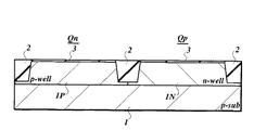
図1は本発明の第1の実施の形態に係る半導体集積回路の相補型MISFET部分を示す断面構造図、図2は相補型MISFETの平面図である。図1及び図2に示すように、本実施の形態において半導体集積回路は単結晶Siからなる低不純物濃度のp型半導体基板1を主体に構成され、この半導体集積回路には論理回路や記憶回路を構築する相補型MISFETが搭載される。
【0027】
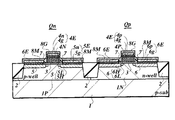
相補型MISFETのnチャネルMISFETQnは、素子分離領域2で周囲を囲まれた領域内においてp型ウェル領域1Pの主面に形成される。このnチャネルMISFETQnはチャネル形成領域として使用されるp型ウェル領域1P、ゲート絶縁膜3、ゲート電極(制御電極)4N、ソース電極、ドレイン電極のそれぞれとして使用される一対の主電極5を備える。
【0028】
p型ウェル領域1Pは、半導体基板1の主面部に形成され、低い不純物濃度に設定される。素子分離領域2は、本実施の形態において、微細化に好適なSTI(Shallow Trench Isolation)で形成される。すなわち、素子分離領域2は、半導体基板1主面から深さ方向に向かって形成された溝と、この溝内に埋設され表面が平坦化された絶縁膜(例えば、SiO2膜)で形成される。なお、素子分離領域2は、フィールド絶縁膜(LOCOS:Local Oxidation of Silicon)で形成してもよい。
【0029】
図3(A)はnチャネルMISFETQnの詳細な要部断面構造図である。nチャネルMISFETQnのゲート絶縁膜3には例えば5nmの膜厚で形成されたSiO2膜が使用される。ゲート絶縁膜3は、必ずしもSiO2膜には限定されず、窒化膜やオキシナイトライド膜等を使用することができる。
【0030】
本実施の形態において、ゲート電極4Nは、ゲート絶縁膜3側にこのゲート絶縁膜3に接して形成された下層の第1領域4gと、ゲート絶縁膜3とは離間され第1領域4g上に形成された上層の第2領域4nとを備えて形成される。第1領域4gは、種類が異なる少なくもと2種類の四族元素で形成された領域である。本実施の形態において、第1領域4gは、四族元素であるSiと、このSiとは異なる四族元素であるGeとを有するSi1−xGexで形成された領域である。第2領域4nは1種類の四族元素であるSiで形成された領域である。本実施の形態に係る相補型MISFETにおいてはデュアルゲート電極構造が採用されているので、nチャネルMISFETQnのゲート電極4Nにはn型不純物がドーピングされる。n型不純物にはAsが実用的に使用できる。
【0031】
図1に示すように、nチャネルMISFETQnはエクステンデッドソース・ドレイン構造で形成され、主電極5は、高不純物濃度のn型半導体領域5Hと、この半導体領域5Hとチャネル形成領域との間に配設された低不純物濃度のn型半導体領域5Lとで形成される。半導体領域5Lはゲート電極4Nに対して自己整合で形成される。半導体領域5Hはゲート電極4N及びその側壁に配設されたゲート側壁7に対して自己整合で形成される。
【0032】
このように構成されるnチャネルMISFETQnにおいては、低抵抗化を図るために、ゲート電極4Nにシリサイド電極8Gが、主電極5にシリサイド電極8Mがそれぞれ電気的に接続される。シリサイド電極8Gは、図1及び図3(A)に示すように、ゲート電極4Nの第2領域4n上に形成される。シリサイド電極8Gは、ゲート電極4Nの第2領域4nのシリサイド化、詳細には主電極5上のシリサイド電極8Mと同一製造工程で行われるサリサイド化により形成され、第2領域4nの少なくとも一部分をシリサイド化することにより形成される。本実施の形態において、シリサイド電極8GはCoSiy膜で形成される。なお、シリサイド電極8Gには他にTiSiy膜が実用的に使用できる。シリサイド電極8Mは、図1に示すように、主電極5、詳細には高不純物濃度の半導体領域5H上に形成され、半導体領域5Hのシリサイド化(サリサイド化)により形成される。シリサイド電極8Mは、シリサイド電極8Gと基本的には同一製造工程で同一導電層に形成されるので、シリサイド電極8Gと同様にCoSiy膜で形成される。
【0033】
一方、相補型MISFETのpチャネルMISFETQpは、図1及び図2に示すように、素子分離領域2で周囲を囲まれた領域内においてn型ウェル領域1Nの主面に形成される。このpチャネルMISFETQpはチャネル形成領域として使用されるn型ウェル領域1N、ゲート絶縁膜3、ゲート電極(制御電極)4P、ソース電極、ドレイン電極のそれぞれとして使用される一対の主電極6を備える。
【0034】
n型ウェル領域1Nは、p型ウェル領域1Pとは別の領域において半導体基板1の主面部に形成され、比較的低い不純物濃度に設定される。
【0035】
図3(B)はpチャネルMISFETQpの詳細な要部断面構造図である。pチャネルMISFETQpのゲート絶縁膜3は、nチャネルMISFETQnのゲート電極3と同一製造工程で同一絶縁層に形成され、例えばSiO2膜で形成される。
【0036】
nチャネルMISFETQnのゲート電極4Nと同様にpチャネルMISFETQpのゲート電極4Pは、ゲート絶縁膜3側にこのゲート絶縁膜3に接して形成された下層の第1領域4gと、ゲート絶縁膜3とは離間され第1領域4g上に形成された上層の第2領域4pとを備えて形成される。第1領域4gは本実施の形態においてSi1−xGexで形成された領域であり、第2領域4pはSiで形成された領域である。デュアルゲート電極構造により、pチャネルMISFETQpのゲート電極4Pにはp型不純物がドーピングされる。p型不純物にはBが実用的に使用できる。
【0037】
図1に示すように、pチャネルMISFETQpはエクステンデッドソース・ドレイン構造で形成され、主電極6は、高不純物濃度のp型半導体領域6Hと、この半導体領域6Hとチャネル形成領域との間に配設された低不純物濃度のp型半導体領域6Lとで形成される。半導体領域6Lはゲート電極4Pに対して自己整合で形成される。半導体領域6Hはゲート電極4P及びその側壁に配設されたゲート側壁7に対して自己整合で形成される。
【0038】
このように構成されるpチャネルMISFETQpにおいては、nチャネルMISFETQnと同様に低抵抗化を図るために、ゲート電極4Pにシリサイド電極8Gが、主電極6にシリサイド電極8Mがそれぞれ電気的に接続される。シリサイド電極8Gは、図1及び図3(A)に示すように、ゲート電極4Pの第2領域4p上に形成される。シリサイド電極8Gは、ゲート電極4Pの第2領域4pのシリサイド化により形成され、第2領域4pの少なくとも一部分をシリサイド化(サリサイド化)することにより形成される。シリサイド電極8Mは、図1に示すように、主電極6の高不純物濃度の半導体領域6H上に形成され、半導体領域6Hのシリサイド化(サリサイド化)により形成される。シリサイド電極8G、シリサイド電極8MはいずれもCoSiy膜で形成される。
【0039】
図4はゲート電極4N、4Pのそれぞれの表面(サリサイド化前の表面)からの深さ(μm)とSiGe組成比との関係を示す図である。本実施の形態において、ゲート電極4N、4Pはいずれも0.15μmの膜厚で形成される。第1領域4gの厚さは0.05μmに設定され、第1領域4gのSiの組成比は0.84に、Geの組成比は0.16にそれぞれ設定される。すなわち、第1領域4gはSi0.86Ge0.16で形成される。第2領域4n、4pのそれぞれの厚さは0.10μmに設定され、第2領域4n、4pのそれぞれのSiの組成比は1.0に設定される。
【0040】
図5はnチャネルMISFETQnのゲート電極4Nの表面(サリサイド化前の表面)からの深さ(μm)とSiGe組成比とAs濃度との関係を示す図である。同図5に示すn型不純物(ドナー)としてのAs濃度分布は、主電極5の高不純物濃度の半導体領域5Hを形成するためのAsをイオン注入により同一製造工程でゲート電極4Nにドーピングした後に、主電極5の活性化アニールを行った場合のAs濃度分布である。図中、実線は本実施の形態に係るSiGeで形成された第1領域4gを有するゲート電極4NのAs濃度を示し、破線はSiゲート電極のAs濃度を示す。Siゲート電極においては、Asの拡散速度が遅いために、ゲート電極表面側からドーピングされたAsがゲート絶縁膜近傍に充分に拡散されていないので、ゲート絶縁膜近傍のAs濃度が低下してしまう。このようなAs濃度の低下はゲートバイアス印加時にゲート絶縁膜近傍において空乏層化を生じ、MOSFETの閾値電圧の制御性を悪化させたり、MOSFETの動作速度を低下させてしまう。
【0041】
これに対して、本実施の形態に係るnチャネルMISFETQnにおいては、ゲート電極4Nのゲート絶縁膜3近傍にSiGeで形成した第1領域4gを配設しており、Geの添加でゲート絶縁膜3近傍のAsの拡散速度を促進させることができるので、第1領域4gの全域にわたってすなわちゲート絶縁膜3近傍の全域にわたって充分なAs濃度を確保することができる。Si0.86Ge0.16中におけるAsの拡散係数は、1000℃の温度環境下において、Si中のAsの拡散係数に比べて2.5倍程度大きくなる。Geの組成比の上昇に伴うAsの拡散係数の増加に関しては、例えばA.Nylandsted,S.Yu.Shiryaev,P.Gaiduk,and V.S.Tishkov,Nucl.Instru.Method.B120 161−164(1996)に述べられている。なお、図5に示すAs濃度分布はSi中とSi0.86Ge0.16中とでのAs偏析係数を1とした場合を示す。従って、ゲート電極4Nにおいて、第1領域4gはSiゲート電極の場合に形成される空乏層化される領域よりも基本的に厚く形成される必要がある。Siゲート電極の場合、通常、5nmの膜厚のゲート絶縁膜に対してゲート電極中に0.5nmの厚さで空乏層が発生するので、第1領域4gの厚さは少なくとも2nm以上に設定されることが好ましい。さらに、第1領域4gのGeの組成比は充分にAsの拡散係数を高めるために0.1以上に設定されることが好ましい。
【0042】
ゲート電極4Nの第2領域4nには図1及び図3(A)に示すようにシリサイド電極8Gが形成されており、第2領域4nは図4及び図5に示すように少なくともその上側の一部をシリサイド電極8Gを形成するためのシリサイド化(又はサリサイド化)領域として使用する。すなわち、シリサイド化は第2領域4nの範囲内で行われ、シリサイド層8Gには抵抗値を増加してしまうGe(又はC)が実質的に含まれない。例えば40nmの膜厚のCoSi2膜でシリサイド電極8Gを形成する場合、1nmの膜厚のCoに対して3.63nmの膜厚のSiが反応し、3.49nmの膜厚のCoSi2膜が生成されるので、41.6nmの膜厚のSiが必要になる。本実施の形態に係るゲート電極4Nにおいては、シリサイド化によりSiが消費される41.6nm以上の膜厚を有する第2領域4nが第1領域4g上に形成される。例えば、Z.Wang,Y.L.Chen,H.Ying,R.J.Nemanich, and D.E.Sayers,Mat.Res.Soc.Symp.Proc.Vol.320,397−402(1994)にはSiを含むシリサイド層に比べてSi及びGeを含むシリサイド層において抵抗値が高くなることが述べられている。
【0043】
図6はpチャネルMISFETQpのゲート電極4Pの表面(サリサイド化前の表面)からの深さ(μm)とSiGe組成比とB濃度との関係を示す図である。同図6に示すp型不純物(アクセプター)としてのB濃度分布は、主電極6の高不純物濃度の半導体領域6Hを形成するためのBF2をイオン注入により同一製造工程でゲート電極4Pにドーピングした後に、主電極6の活性化アニールを行った場合のB濃度分布である。図中、実線は本実施の形態に係るSiGeで形成された第1領域4gを有するゲート電極4PのB濃度を示し、破線はSiゲート電極のB濃度を示す。Siゲート電極においては、Bの拡散速度がAsの拡散速度に比べて速く、しかもドーピングされたBF2のFがゲート絶縁膜中でのBの拡散を助長してしまうために、ゲート電極にドーピングされたBがチャネル形成領域に漏れてしまう。このようなB漏れはMOSFETの閾値電圧の制御性を悪化させてしまう。
【0044】
これに対して、本実施の形態に係るpチャネルMISFETQpにおいては、ゲート電極4Pのゲート絶縁膜3近傍にSiGeで形成した第1領域4gを配設しており、Geの添加でゲート絶縁膜3近傍のBの拡散速度を減速させることができるので、ゲート電極4Pからゲート絶縁膜3を通してチャネル形成領域にB漏れ(Bのゲート絶縁膜3の突き抜け)を生じることがない。Si0.86Ge0.16中におけるBの拡散係数は、1000℃の温度環境下において、Si中のBの拡散係数に比べて0.5〜0.1倍程度に小さくなるので、Bのゲート絶縁膜3中への拡散量を減少させ、チャネル形成領域へのBの突き抜けを効果的に抑制することができる。このGeの組成比の上昇に伴うBの拡散係数の減少に関しては、例えばP.Kuo,J.L.Hoyt,and J.F.Gibbons,Appl.Phys.Lett.66 580−582(1995)に述べられている。なお、図6に示すB濃度分布はSi中とSi0.86Ge0.16中とでのB偏析係数を1とした場合を示す。従って、ゲート電極4Pにおいて、第1領域4gはSiゲート電極の場合に発生するB漏れを防止する厚さで形成される必要があり、本実施の形態において第1領域4gの厚さは少なくとも2nm以上に設定され、第1領域4gのGeの組成比は0.1以上に設定される。
【0045】
前述のnチャネルMISFETQnのゲート電極4Nと同様に、ゲート電極4Pの第2領域4pには図1及び図3(B)に示すようにシリサイド電極8Gが形成されており、第2領域4pは図4及び図6に示すように少なくともその上側の一部をシリサイド電極8Gを形成するためのシリサイド化領域として使用する。すなわち、シリサイド化は第2領域4pの範囲内で行われ、シリサイド層8Gには抵抗値を増加してしまうGe(又はC)が実質的に含まれない。ゲート電極4Pにおいては、シリサイド化によりSiが消費される41.6nm以上の膜厚を有する第2領域4pが第1領域4g上に形成される。
【0046】
図1に示すように、nチャネルMISFETQnの主電極5には、シリサイド電極8M、コンタクトプラグ電極(埋込み電極)12のそれぞれを介在して配線15が電気的に接続される。同様に、pチャネルMISFETQpの主電極6には、シリサイド電極8M、コンタクトプラグ電極12のそれぞれを介在して配線15が電気的に接続される。
【0047】
コンタクトプラグ電極12は、nチャネルMISFETQn、pチャネルMISFETQpのそれぞれを覆う層間絶縁膜10に形成された接続孔11内に埋設され、nチャネルMISFETQn、pチャネルMISFETQpのそれぞれにおいて同一導電層に配設され同一導電性材料で形成される。本実施の形態において、コンタクトプラグ電極12は、Ti膜12A及びこのTi膜12A上に積層したW膜12Bの複合膜で形成される。層間絶縁膜10は例えばSi3N4膜10A及びBPSG膜10Bの複合膜で形成される。
【0048】
配線15はコンタクトプラグ電極12を覆う層間絶縁膜13上に形成され、この層間絶縁膜13に形成された接続孔14を通して配線15とコンタクトプラグ電極12との間が接続される。配線15は、nチャネルMISFETQn、pチャネルMISFETQpのそれぞれにおいて同一導電層に配設され同一導電性材料で形成される。本実施の形態において、配線15はTi膜、TiN膜、AlCu膜、Ti膜、TiN膜のそれぞれを順次重ね合わせた複合膜で形成される。層間絶縁膜13は例えばSi3N4膜13A及びTEOS膜13Bの複合膜で形成される。
【0049】
なお、図1には示していないが、図2に接続孔11の領域を示すように、nチャネルMISFETQnのゲート電極4N、pチャネルMISFETQpのゲート電極4Pのそれぞれにも前述のシリサイド層8G、コンタクトプラグ電極12のそれぞれを介在して配線15が電気的に接続される。
【0050】
<製造プロセス>
次に、前述のMISFETを備えた半導体集積回路の製造プロセスを説明する。図7乃至図19は製造プロセスを各製造工程毎に示す半導体集積回路の工程断面図である。
【0051】
(1)まず、単結晶Siからなる低不純物濃度のp型半導体基板1を準備する。そして、nチャネルMISFETQnの形成領域において半導体基板1の主面部にp型ウェル領域1Pを形成し、pチャネルMISFETQpの形成領域において半導体基板1の主面部にn型ウェル領域1Nを形成する(図7参照)。
【0052】
(2)MISFET間を含む素子形成領域間において半導体基板1に溝を形成し、この溝に絶縁体を埋設することにより素子分離領域2を形成する(図7参照)。溝は好ましくは異方性エッチングで半導体基板1表面から深さ方向にエッチングを行うことにより形成する。絶縁体にはCVD法又はスパッタリング法で成膜したSiO2膜を実用的に使用することができ、成膜後にエッチバック法、ケミカルメカニカルポリッシング(CMP)法等によりSiO2膜の表面には平坦化処理がなされる。
【0053】
なお、素子分離領域2はnチャネルMISFETQn、pチャネルMISFETQp等の半導体素子を形成した後に形成してもよい。また、素子分離領域2はフィールド酸化膜を主体として形成してもよい。
【0054】
(3)図7に示すように、nチャネルMISFETQn、pチャネルMISFETQpのそれぞれの形成領域において、半導体基板1の主面上にゲート絶縁膜3を形成する。本実施の形態においてゲート絶縁膜3には酸化性雰囲気中で半導体基板1表面を加熱する熱酸化法で形成したSiO2膜が使用される。ゲート絶縁膜3の膜厚は、必要とする閾値電圧値により適宜設定できるが、本実施の形態においては2.5nmで形成される。なお、詳細な説明は省略するが、ゲート絶縁膜3の形成前に閾値電圧を調節するためのドーパントをチャネル形成領域にドーピングしてあることが好ましい。
【0055】
(4)図8に示すように、ゲート絶縁膜3上を含む半導体基板1全面にゲート電極形成層40を形成する。本実施の形態において、ゲート電極形成層40はシラン(Si2H6)ガスとゲルマン(GeH4)ガスとの混合ガスをソースガスとするCVD法で成膜される。このCVD法においては、Si2H6ガスとGeH4ガスのそれぞれのガス分圧及び成膜温度を適宜制御することにより、ゲート電極形成層40は、ゲート絶縁膜3からの距離に応じてGeの組成比を任意に変化させ、Si1−xGexからなる第1領域4g、Siからなる第2領域4mのそれぞれを有するゲート電極形成層40を形成することができる。この時点において第2領域4mはn型不純物、p型不純物のいずれもドーピングされていない状態にある。
【0056】
第1領域4gは、Si2H6ガスの流量が5sccm、GeH4ガスの流量が1sccm、成膜圧力が1.3×10²Pa、成膜温度が500℃、成膜時間が10分間の条件において成膜される。この条件下において、第1領域4gは前述の図4に示すようにGeの組成比が0.16のSi0.86Ge0.16で形成することができ、第1領域4gの厚さは0.05μmになる。第2領域4mは、第1領域4gに引き続き連続的に成膜され、Si2H6ガスの流量、成膜圧力、成膜温度のそれぞれの条件はいずれも変えずにGeH4ガスの流量を0sccm、成膜時間を28分間にそれぞれ調節する。この条件下において、第2領域4mはGeの組成比が0でSiの組成比が1.0すなわち実質的にGeを含まないSiを成膜することができる。第2領域4mは0.10μmの膜厚で成膜される。本実施の形態においては、GeH4ガスの流量が1sccmから急減に0sccmに変化させているので、図4に示すようにGeの組成比はゲート絶縁膜3から0.05μmの距離において急激に減少する。第2領域4mにおいては、少なくともシリサイド化(salicide)によりシリサイド電極8Gの形成に消費される部分が少なくともGeの組成比を0に設定してあればよい。
【0057】
なお、第1領域4gはSiH4ガスとGe2H6ガスとの混合ガスをソースガスとするCVD法で形成することもできる。さらに、第1領域4gはMBE(Molecular Beam Epitaxy)法で形成することもできる。
【0058】
(5)図9に示すように、ゲート電極形成層40にパターンニングを行い、nチャネルMISFETQn、pチャネルMISFETQpのそれぞれの形成領域にゲート電極4を形成する。ゲート電極4のゲート幅寸法及びゲート長寸法は製作するMISFETサイズや電気特性に応じて任意に決定される。パターンニングは、フォトリソグラフィ技術で形成されたマスクを使用し、RIE等の異方性エッチングで行われる。
【0059】
(6)図10に示すように、ゲート電極4の表面を覆う絶縁膜4Aを形成する。絶縁膜4Aには例えば熱酸化法で成膜されたSiO2膜やCVD法で成膜されたSiO2膜が実用的に使用できる。
【0060】
(7)次に、エクステンデッドソース・ドレインプロセスを開始する。まず、図11に示すように、nチャネルMISFETQnの形成領域においてソース電極及びドレイン電極として使用する一対の主電極5を形成するために、低不純物濃度のn型半導体領域5Lを形成する。半導体領域5Lは、ゲート電極4、素子分離領域2及びpチャネルMISFETQpの形成領域を覆うマスク20を耐不純物注入マスクとして使用し、イオン注入法によりp型ウェル領域1Pの主面部にn型不純物をドーピングすることにより形成される。マスク20にはフォトリソグラフィ技術で形成されたレジストマスクが使用される。n型不純物には拡散速度が遅くシャロー化に好適なAsが使用される。Asに対してイオン注入法における注入エネルギ量は10〜50keV、ドーズ量は1014〜1015atoms/cm2に設定することが一般的であるが、本実施の形態においてAsの注入エネルギ量は15keV、ドーズ量は1014atoms/cm2の条件が使用される。
【0061】
(8)図12に示すように、pチャネルMISFETQpの形成領域においてソース電極及びドレイン電極として使用する一対の主電極6を形成するために、低不純物濃度のp型半導体領域6Lを形成する。半導体領域6Lは、ゲート電極4、素子分離領域2及びnチャネルMISFETQnの形成領域を覆うマスク21を耐不純物注入マスクとして使用し、イオン注入法によりn型ウェル領域1Nの主面部にp型不純物をドーピングすることにより形成される。マスク21にはマスク20と同様にフォトリソグラフィ技術で形成されたレジストマスクが使用される。p型不純物にはイオン注入分布を浅くすることができシャロー化に好適なBF2が使用される。本実施の形態においてBF2の注入エネルギ量は10keV、ドーズ量は1014atoms/cm2の条件が使用される。また、p型不純物にはBイオンやB分子イオンが実用的に使用できる。
【0062】
なお、前述のAs、BF2のそれぞれのイオン注入後には、イオン注入に伴う半導体基板1表面のダメージの回復や不純物の活性化を目的としてアニールを行うことが好ましい。
【0063】
(9)図13に示すように、nチャネルMISFETQn、pチャネルMISFETQpのそれぞれの形成領域においてゲート電極4の側壁に絶縁膜4Aを介してゲート側壁7を形成する。ゲート側壁7は本実施の形態においてSi3N4膜で形成される。ゲート側壁7は、例えば低圧CVD法、スパッタ法等の成膜技術で半導体基板1上の全面に形成されたSi3N4膜に成膜した膜厚分に相当するRIE等の異方性エッチングを行うことにより形成される。
【0064】
(10)図14に示すように、nチャネルMISFETQnの形成領域において一対の主電極5を形成するために、高低不純物濃度のn型半導体領域5Hを形成する。半導体領域5Hは、ゲート電極4、ゲート側壁7、素子分離領域2及びpチャネルMISFETQpの形成領域を覆うマスク22を耐不純物注入マスクとして使用し、イオン注入法によりp型ウェル領域1Pの主面部にn型不純物をドーピングすることにより形成される。本実施の形態に係る相補型MISFETはデュアルゲート電極構造を採用するので、n型不純物はゲート電極4にもドーピングされ、それぞれn型不純物がドーピングされた第1領域4g及び第2領域4nを有するゲート電極4Nが形成される。マスク22にはフォトリソグラフィ技術で形成されたレジストマスクが使用される。n型不純物には拡散速度が遅くシャロー化に好適なAsが使用される。本実施の形態においてAsの注入エネルギ量は50keV、ドーズ量は3×10¹⁵atoms/cm2の条件が使用される。
【0065】
(11)図15に示すように、pチャネルMISFETQpの形成領域において一対の主電極6を形成するために、高低不純物濃度のp型半導体領域6Hを形成する。半導体領域6Hは、ゲート電極4、ゲート側壁7、素子分離領域2及びnチャネルMISFETQnの形成領域を覆うマスク23を耐不純物注入マスクとして使用し、イオン注入法によりn型ウェル領域1Nの主面部にp型不純物をドーピングすることにより形成される。デュアルゲート電極構造を採用するので、p型不純物はゲート電極4にもドーピングされ、それぞれp型不純物がドーピングされた第1領域4g及び第2領域4pを有するゲート電極4Pが形成される。マスク23にはフォトリソグラフィ技術で形成されたレジストマスクが使用される。p型不純物にはイオン注入分布を浅くすることができシャロー化に好適なBF2が使用される。本実施の形態においてBF2の注入エネルギ量は40keV、ドーズ量は3×10¹⁵atoms/cm2の条件が使用される。
【0066】
(12)アニールを行い、イオン注入された不純物の活性化を行う。本実施の形態において、アニールは、RTA(Rapid Thermal Annealing)法で行われ、N2ガス雰囲気中、1000℃の温度で10秒間行われる。このアニールにより、半導体領域5L及び5Hからなる主電極5が形成され、nチャネルMISFETQnがほぼ完成する。本実施の形態において、nチャネルMISFETQnのチャネル形成領域のアクセプター濃度は1017〜1018atoms/cm3程度、主電極5のドナー濃度は1019〜1021atoms/cm3程度、主電極5の接合深さは50〜200nm程度で形成される。nチャネルMISFETQnのゲート電極4Nはデュアルゲート電極構造でn型に設定され、nチャネルMISFETQnは表面チャネル型になるので、nチャネルMISFETQnは短チャネル効果の抑制及び動作速度の高速化に好適で微細化を実現することができる。同様に、アニールにより、半導体領域6L及び6Hからなる主電極6が形成され、pチャネルMISFETQpがほぼ完成する。pチャネルMISFETQpのチャネル形成領域のドナー濃度は1017〜1018atoms/cm3程度、主電極6のアクセプター濃度は1019〜1021atoms/cm3程度、主電極5の接合深さは50〜200nm程度で形成される。pチャネルMISFETQpのゲート電極4Pはデュアルゲート電極構造でp型に設定され、pチャネルMISFETQpは表面チャネル型になるので、pチャネルMISFETQpは短チャネル効果の抑制及び動作速度の高速化に好適で微細化を実現することができる。
【0067】
(13)図16に示すように、nチャネルMISFETQnのゲート電極4N上にシリサイド電極8G、主電極5上にシリサイド電極8M、pチャネルMISFETQpのゲート電極4P上にシリサイド電極8G、主電極6上にシリサイド電極8Mのそれぞれを同一製造工程で形成する。本実施の形態においてシリサイド電極8G、8Mのそれぞれはサリサイド化によるCoSiy膜で形成される。CoSiy膜は、まずゲート電極4N上、4P上、主電極5上、6上のそれぞれに存在する絶縁膜を除去し、ゲート電極4Nの第2領域4n、ゲート電極4Pの第2領域4p、主電極5の半導体領域5H、主電極6の半導体領域6Hのそれぞれの表面を露出させる。引き続き、半導体基板1上の全面にCo膜、キャップ層としてのTiN膜を順次成膜する。Co膜、TiN膜はいずれも例えばスパッタリング法で成膜し、Co膜は例えば11.5nmの膜厚で形成される。このCo膜は非酸化性雰囲気中、500℃の温度で60秒間のアニールを行った後、TiN膜及び未反応のCo膜を除去し、引き続き750℃の温度で30秒間のアニールを行う2段階アニール法によりシリサイド化され、40nmの膜厚を有するシリサイド電極8G、8Mのそれぞれを形成することができる。2段階アニール法は、CoSiからCoSi2への相転移を目的として、さらに1回目のアニール直後に未反応のCo膜を除去してゲート側壁7上におけるシリサイド電極8Gと8Mとの間のブリッジングの防止を目的として行われる。いずれのアニールもRTA法で行われ、前述の未反応のCo膜の除去には例えば硫酸と過酸化水素水との混合溶液が実用的に使用できる。
【0068】
前述のように、nチャネルMISFETQnにおいて、シリサイド電極8GはGeを含まないSiで形成された第2領域4nの一部を第2領域4nの範囲内でシリサイド化することにより形成されるので、シリサイド電極8GにはGeが含まれない。同様に、pチャネルMISFETQpにおいて、シリサイド電極8GはGeを含まないSiで形成された第2領域4pの一部を第2領域4pの範囲内でシリサイド化することにより形成されるので、シリサイド電極8GにはGeが含まれない。従って、シリサイド電極8Gの抵抗値を減少させることができる。しかも、相補型MISFETにおいては、nチャネルMISFETQnの第1領域4g及び第2領域4nを有するゲート電極4N、pチャネルMISFETQpの第1領域4g及び第2領域4pを有するゲート電極4Pのそれぞれが同一製造工程で形成することができる。
【0069】
(14)図17に示すように、半導体基板1上の全面に層間絶縁膜10を形成する。層間絶縁膜10は、本実施の形態において、スパッタリング法で成膜されたSi3N4膜10A、CVD法で成膜されたBPSG膜10Bのそれぞれを順次積層することにより形成される。層間絶縁膜10の表面はケミカルメカニカルポリッシング法により平坦化される。
【0070】
(15)nチャネルMISFETQnのシリサイド電極8G上、8M上、pチャネルMISFETQpのシリサイド電極8G上、8M上において層間絶縁膜10に接続孔11を形成し、図18に示すように接続孔11内にコンタクトプラグ電極12を埋設する。コンタクトプラグ電極12は、本実施の形態においてスパッタリング法で成膜されたTi膜12A、選択CVD法で成膜されたW膜12Bのそれぞれを順次積層し、W膜12Bの表面側からケミカルメカニカルポリッシングで研磨することにより接続孔11内に埋設することができる。
【0071】
(16)図19に示すように、層間絶縁膜10上の全面に層間絶縁膜13を形成する。層間絶縁膜13は、本実施の形態において、スパッタリング法で成膜されたSi3N4膜13A、プラズマCVD法で成膜されたTEOS膜13Bのそれぞれを順次積層することにより形成される。
【0072】
(17)コンタクトプラグ電極12上において層間絶縁膜13に接続孔14を形成し(図1参照)、前述の図1に示すように、層間絶縁膜13上に接続孔14を通してコンタクトプラグ電極12に電気的に接続される配線15を形成する。本実施の形態において、配線15はスパッタリング法によりTi膜、TiN膜、AlCu膜、Ti膜、TiN膜のそれぞれを順次積層した複合膜で形成される。また、配線15はダマシンプロセスで形成されたダマシン配線を使用してもよい。これら一連の製造工程が終了すると、本実施の形態に係る半導体集積回路が完成する。
【0073】
このように構成される本実施の形態に係る半導体集積回路においては、pチャネルMISFETQpのゲート電極4Pのゲート絶縁膜3側に配設された第1領域4gに第2四族元素であるGeが含まれる(又はCが含まれ、第1領域4gはSiGe又はSiCで形成される)ので、第1領域4g中のp型不純物であるBの拡散速度を減少させ、Bのチャネル形成領域側への漏れを防止することができる。従って、pチャネルMISFETQpの閾値電圧を安定化させることができ、半導体集積回路の電気的信頼性を向上させることができる。さらに、nチャネルMISFETQnのゲート電極4Nのゲート絶縁膜3側に配設された第1領域4gに第2四族元素であるGeが含まれる(同様に又はCが含まれ、第1領域4gはSiGe又はSiCで形成される)ので、第1領域4g中のn型不純物であるAsの拡散速度を促進し、ゲート電極4Nの全域にわたって特にゲート絶縁膜3近傍でAsの不純物濃度を充分に確保することができる。従って、ゲート電極4N内の空乏層化を防止することができ、nチャネルMISFETQnの閾値電圧を安定化させることができるので、半導体集積回路の電気的信頼性を向上させることができる。特に、デュアルゲート電極構造の相補型MISFETを備えた半導体集積回路においては、第1及び第2四族元素を含む同一構造のゲート電極4(下層の第1領域4g及び上層の第2領域4mで形成される。)の使用でpチャネルMISFETQp、nチャネルMISFETQnのそれぞれの閾値電圧を同時に安定化させることができる。この結果、MISFETの微細化を実現することができ、半導体集積回路の集積度を向上させることができる。
【0074】
さらに、半導体集積回路においては、pチャネルMISFETQpのゲート電極4Pの実質的に第2四族元素であるGeを含まない第2領域4p、nチャネルMISFETQnのゲート電極4Nの実質的に第2四族元素であるGeを含まない第2領域4nのそれぞれをシリサイド化(サリサイド化)することによりシリサイド電極8Gを形成しているので、シリサイド電極8Gには第2四族元素が含まれない。従って、シリサイド電極8Gの抵抗値を減少させることができ、pチャネルMISFETQp、nチャネルMISFETQnのそれぞれのスイッチング動作速度の高速化並びに低電源電圧化を実現することができ、半導体集積回路の回路動作速度の高速化並びに低消費電力化を実現することができる。
【0075】
さらに、半導体集積回路の製造方法においては、ソースガスの調節だけで第2四族元素を実質的に含まない第2領域4pを有するpチャネルMISFETQpのゲート電極4P、第2領域4nを有するnチャネルMISFETQnのゲート電極4Nのそれぞれを形成し、第2領域4p、4nのそれぞれの少なくとも一部をシリサイド化するだけで第2四族元素が実質的に含まれないシリサイド電極8Gを形成することができる。従って、製造工程数を増加することなく、容易にシリサイド電極8Gの抵抗値を減少させることができる。
【0076】
さらに、半導体集積回路の製造方法においては、第1領域4g及び第2領域4mを有するゲート電極4を相補型MISFETのそれぞれにおいて同一製造工程で形成し、デュアルゲート電極構造の相補型MISFETを形成することができるので、ゲート電極を相補型MISFETのそれぞれで別々に形成する場合に比べて製造工程数を減少させることができる。
【0077】
(第2の実施の形態)
本実施の形態は、MISFETのゲート電極の四族元素の組成比をゲート絶縁膜からの距離に応じて変化させた構造例を説明するものである。図20、図21はそれぞれ本発明の第2の実施の形態に係るnチャネルMISFETQnのゲート電極4N、pチャネルMISFETQpのゲート電極4Pのそれぞれの表面(サリサイド化前の表面)からの深さ(μm)とSiGe組成比との関係を示す図である。
【0078】
図20に示すゲート電極4N、4Pは第1の実施の形態に係る半導体集積回路と同様にいずれも0.15μmの膜厚で形成される。第1領域4gの厚さは0.05μmに設定される。第1領域4gのSiの組成比はゲート絶縁膜3側から所定距離まで一定に維持され、さらにゲート絶縁膜3から離れるに従い連続的にかつ緩やかに増加する。ゲート絶縁膜3側においてSiの組成比は0.60、第2領域4n又は4p側においてSiの組成比は1.0に設定される。このSiの組成比の変化に従い、第1領域4gのGeの組成比はゲート絶縁膜3側から離れるに従い連続的にかつ緩やかに減少し、ゲート絶縁膜3側においてGeの組成比は0.40、第2領域4n又は4p側においてGeの組成比は0に設定される。このようなSiGeの組成比が連続的に変化する第1領域4gは、CVD法におけるGeH4ガスの流量を徐々に減少させることにより容易に形成することができる。
【0079】
図21に示すゲート電極4N、4Pは第1の実施の形態に係る半導体集積回路と同様にいずれも0.15μmの膜厚で形成される。第1領域4gの厚さは0.05μmに設定される。第1領域4gのSiの組成比はゲート絶縁膜3側から所定距離まで一定に維持され、さらにゲート絶縁膜3から離れると段階的に増加する。ゲート絶縁膜3側においてSiの組成比は0.60、段階的に増加して最終的には第2領域4n又は4p側においてSiの組成比は1.0に設定される。このSiの組成比の変化に従い、第1領域4gのGeの組成比はゲート絶縁膜3側から離れるに従い段階的に減少し、ゲート絶縁膜3側においてGeの組成比は0.40、第2領域4n又は4p側においてGeの組成比は0に設定される。このようなSiGeの組成比が段階的に変化する第1領域4gは、CVD法におけるGeH4ガスの流量を段階的に減少させることにより容易に形成することができる。
【0080】
なお、本実施の形態においては、ゲート絶縁膜3の直上にSiGeの第1領域4gを形成しているが、本発明においては、ゲート絶縁膜3と第1領域4gとの間に第1領域4gの厚さよりも非常に薄い膜厚、詳細には1nm以下の膜厚でGeを実質的に含まないSi層又はSiを実質的に含まないGe層が形成されていてもよい。このSi層又はGe層が実際に存在していても、ゲート電極4PにドーピングされたBの拡散は上層の第1領域4g中で抑制することができ、ゲート電極4NにドーピングされたAsの拡散は第1領域4g中で促進させることができる。さらに、ゲート絶縁膜3がSiO2膜で形成される場合、Si層は第1領域4gに含まれたGeによるSiO2膜の膜質の劣化を防ぐことができる。さらに、Ge層が形成される場合には、このGe層はゲート電極4PにドーピングされたBの拡散を抑制することができる。Ge層は特にゲート絶縁膜3を窒化膜で形成する場合に有効である。
【0081】
このように構成される半導体集積回路においては、前述の第1の実施の形態に係る半導体集積回路で得られる効果と同様の効果を得ることができる。
【0082】
(第3の実施の形態)
本実施の形態は、MISFETのゲート電極の他の構造例を説明するものである。図22(A)、図22(B)、図22(C)、図22(D)、図22(E)はいずれも本発明の第3の実施の形態に係る半導体集積回路のnチャネルMISFETQnの詳細な要部断面構造図である。
【0083】
図22(A)に示すnチャネルMISFETQnはシリサイド電極8Gを形成した後の構造であり、ゲート電極4NはSiGeからなる第1領域4gだけで形成され、このゲート電極4N上にはシリサイド電極8Gが形成される。シリサイド電極8Gの形成前(シリサイド化前)においては破線で示すようにゲート電極4NにSiからなる第2領域4nが形成されており、シリサイド電極8Gはこの第2領域4nを丁度すべて消費することにより形成される。従って、シリサイド電極8Gには実質的にGeが含まれないので、第1の実施の形態に係る半導体集積回路と同様にシリサイド電極8Gの抵抗値を減少させることができる。
【0084】
図22(B)に示すnチャネルMISFETQnは同様にシリサイド電極8Gを形成した後の構造である。ゲート電極4Nは、SiGeからなる第1領域4gと、この第1領域4g上のCoSizGez’からなる3元化合物(多元化合物)の第2領域4tとで形成される。シリサイド電極8Gはゲート電極4Nの第2領域4t上に形成される。第2領域4tは、シリサイド化前は前述の第1の実施の形態に係る半導体集積回路のnチャネルMISFETQnと同様にSiからなる第2領域4nであったものが、シリサイド化により下層の第1領域4gのSiGe、上層に形成されたCoのそれぞれと化合し生成されたものである。CoSizGez’からなる3元化合物は化学的に安定しており、シリサイド電極8GにはGeが実質的に含まれないので、第1の実施の形態に係る半導体集積回路と同様にシリサイド電極8Gの抵抗値を減少させることができる。
【0085】
図22(C)に示すnチャネルMISFETQnは、SiGeからなる第1領域4g、Siからなる第2領域4nのそれぞれを交互に複数積層してゲート電極4Nが形成される。ゲート電極4Nは、基本的にはゲート絶縁膜3側(最下層)に第1領域4gが配設され、ゲート絶縁膜3から離間されシリサイド化される領域(最上層)に第2領域4nが配設されていればよい。シリサイド電極8Gは最上層の第2領域4nの一部をシリサイド化することにより形成されるので、シリサイド電極8GにはGeが実質的に含まれず、シリサイド電極8Gの抵抗値を減少させることができる。
【0086】
図22(D)に示すnチャネルMISFETQnは、図22(A)に示すnチャネルMISFETQnと図22(C)に示すnチャネルMISFETQnとを組み合わせたものである。すなわち、nチャネルMISFETQnのゲート電極4NはSiGeからなる第1領域4g、Siからなる第2領域4n、SiGeからなる第1領域4gのそれぞれを順次積層して形成され、シリサイド電極8Gは最上層の第1領域4g上に形成される。シリサイド化前においてはゲート電極4Nの最上層はSiからなる第2領域4nであり、シリサイド化によりこの最上層の第2領域4nを丁度すべて消費してシリサイド電極8Gが形成される。従って、シリサイド電極8GにはGeが実質的に含まれないので、シリサイド電極8Gの抵抗値を減少させることができる。
【0087】
図22(E)に示すnチャネルMISFETQnは、図22(B)に示すnチャネルMISFETQnと図22(C)に示すnチャネルMISFETQnとを組み合わせたものである。すなわち、nチャネルMISFETQnのゲート電極4NはSiGeからなる第1領域4g、Siからなる第2領域4n、SiGeからなる第1領域4g、CoSizGez’からなる3元化合物の第2領域4tのそれぞれを順次積層して形成され、シリサイド電極8Gは最上層の第2領域4t上に形成される。このシリサイド電極8GにはGeが実質的に含まれないので、シリサイド電極8Gの抵抗値を減少させることができる。
【0088】
なお、図22(A)、図22(B)、図22(C)、図22(D)、図22(E)のそれぞれに示すゲート電極構造はpチャネルMISFETQpにおいても同一構造になる。さらに、第2四族元素であるGeに代えてCが使用できる。
【0089】
本実施の形態に係る半導体集積回路においては、前述の第1の実施の形態に係る半導体集積回路で得られる効果と同様の効果を得ることができる。
【0090】
(第4の実施の形態)
本実施の形態は、エレベーテッド電極を有するMISFETを備えた半導体集積回路に本発明を適用した例を説明するものである。
【0091】
<デバイス構造>
図23は本発明の第4の実施の形態に係る半導体集積回路の相補型MISFET部分を示す断面構造図である。図23に示すように、本実施の形態に係る半導体集積回路は、前述の第1の実施の形態に係る半導体集積回路と同様に、単結晶Siからなる低不純物濃度のp型半導体基板1を主体に構成され、この半導体集積回路には論理回路や記憶回路を構築する相補型MISFETが搭載される。
【0092】
相補型MISFETの基本的な構造は第1の実施の形態に係る半導体集積回路に搭載された相補型MISFETの構造と同一である。すなわち、相補型MISFETのnチャネルMISFETQnは、素子分離領域2で周囲を囲まれた領域内においてp型ウェル領域1Pの主面に形成され、チャネル形成領域として使用されるp型ウェル領域1P、ゲート絶縁膜3、ゲート電極4N、ソース電極、ドレイン電極のそれぞれとして使用される一対の主電極5を備える。
【0093】
p型ウェル領域1Pは、半導体基板1の主面部に形成され、低い不純物濃度に設定される。素子分離領域2は、第1の実施の形態に係る半導体集積回路と同様に、微細化に好適なSTIで形成される。
【0094】
nチャネルMISFETQnのゲート絶縁膜3には例えば5nmの膜厚で形成されたSiO2膜が使用される。ゲート電極4Nは、前述の第1の実施の形態に係る半導体集積回路のゲート電極4Nの第1領域4gに相当する領域で、種類が異なる少なくもと2種類の四族元素で全域を形成した領域である。本実施の形態において、ゲート電極4Nは、四族元素であるSiと、このSiとは異なる四族元素であるGeとを有するSi1−xGexで形成される。相補型MISFETはデュアルゲート電極構造を採用しているので、nチャネルMISFETQnのゲート電極4Nにはn型不純物がドーピングされる。n型不純物にはAsが実用的に使用できる。
【0095】
nチャネルMISFETQnはエクステンデッドソース・ドレイン構造で形成され、主電極5は、高不純物濃度のn型半導体領域5Hと、この半導体領域5Hとチャネル形成領域との間に配設された低不純物濃度のn型半導体領域5Lとで形成される。半導体領域5Lはゲート電極4Nに対して自己整合で形成される。半導体領域5Hはゲート電極4N及びその側壁に配設されたゲート側壁7に対して自己整合で形成される。
【0096】
このように構成されるnチャネルMISFETQnにおいては、ゲート電極4Nにエレベーテッド電極(エレベーテッドゲート電極)4Eが電気的に接続され、このエレベーテッド電極4Eにはシリサイド電極8Gが電気的に接続されるとともに、シャロー化並びに低抵抗化を図るために主電極5にエレベーテッド電極(エレベーテッドソース電極又はエレベーテッドドレイン電極)5Eが電気的に接続され、このエレベーテッド電極5Eにはシリサイド電極8Mが電気的に接続される。
【0097】
ゲート電極4N上のエレベーテッド電極4Eは、前述の第1の実施の形態に係る半導体集積回路のゲート電極4Nと同様の構造で形成され、ゲート電極4N側にこのゲート電極4Nに接して形成された下層の第1領域4gと、ゲート電極4Nとは離間され第1領域4g上に形成された上層の第2領域4nとを備えて形成される。第1領域4g、第2領域4nはいずれもエピタキャル成長層で形成される。第1領域4gは、種類が異なる少なくもと2種類の四族元素で形成された領域である。本実施の形態において、第1領域4gは、四族元素であるSiと、このSiとは異なる四族元素であるGeとを有するSi1−xGexで形成された領域である。第2領域4nは1種類の四族元素であるSiで形成された領域である。デュアルゲート電極構造が採用されているので、エレベーテッド電極4Eにはn型不純物であるAsがドーピングされる。
【0098】
シリサイド電極8Gは、エレベーテッド電極4Eの第2領域4n上に形成される。本実施の形態において、シリサイド電極8Gは第2領域4nの上面及び側面に形成される。シリサイド電極8Gは、エレベーテッド電極4Eの第2領域4nのシリサイド化、詳細には主電極5上のシリサイド電極8Mと同一製造工程で行われるサリサイド化により形成され、第2領域4nの少なくとも一部分をシリサイド化することにより形成される。本実施の形態において、シリサイド電極8GはCoSiy膜で形成される。なお、シリサイド電極8Gには他にTiSiy膜が実用的に使用できる。
【0099】
主電極5上のエレベーテッド電極5Eは、エレベーテッド電極4Eと同様に、主電極5側にこの主電極5に接して形成された下層の第1領域5gと、主電極5とは離間され第1領域5g上に形成された上層の第2領域5nとを備えて形成される。第1領域5g、第2領域5nはいずれもエピタキャル成長層で形成される。第1領域5gはエレベーテッド電極4Eの第1領域4gと同様に本実施の形態においてSi1−xGexで形成され、第2領域5nはSiで形成される。エレベーテッド電極5Eにはn型不純物であるAsがドーピングされる。
【0100】
シリサイド電極8Mは、シリサイド電極8Gと同様にエレベーテッド電極5E上に形成され、エレベーテッド電極5Eの第2領域5nの少なくとも一部のシリサイド化(サリサイド化)により形成される。シリサイド電極8Mは、シリサイド電極8Gと基本的には同一製造工程で同一導電層に形成されるので、シリサイド電極8Gと同様にCoSiy膜で形成される。
【0101】
一方、相補型MISFETのpチャネルMISFETQpは、図23に示すように、素子分離領域2で周囲を囲まれた領域内においてn型ウェル領域1Nの主面に形成される。このpチャネルMISFETQpはチャネル形成領域として使用されるn型ウェル領域1N、ゲート絶縁膜3、ゲート電極4P、ソース電極、ドレイン電極のそれぞれとして使用される一対の主電極6を備える。
【0102】
pチャネルMISFETQpのゲート絶縁膜3は、nチャネルMISFETQnのゲート電極3と同一製造工程で同一絶縁層に形成され、例えばSiO2膜で形成される。
【0103】
ゲート電極4Pはゲート電極4Nと同様にSi1−xGexで形成され、相補型MISFETにはデュアルゲート電極構造が採用されるので、pチャネルMISFETQpのゲート電極4Pにはp型不純物がドーピングされる。p型不純物にはBF2が実用的に使用できる。
【0104】
pチャネルMISFETQpはエクステンデッドソース・ドレイン構造で形成され、主電極6は、高不純物濃度のp型半導体領域6Hと、この半導体領域6Hとチャネル形成領域との間に配設された低不純物濃度のp型半導体領域6Lとで形成される。半導体領域6Lはゲート電極4Pに対して自己整合で形成される。半導体領域6Hはゲート電極4P及びその側壁に配設されたゲート側壁7に対して自己整合で形成される。
【0105】
このように構成されるpチャネルMISFETQpにおいては、ゲート電極4Pにエレベーテッド電極(エレベーテッドゲート電極)4Eが電気的に接続され、このエレベーテッド電極4Eにはシリサイド電極8Gが電気的に接続されるとともに、シャロー化並びに低抵抗化を図るために主電極6にエレベーテッド電極(エレベーテッドソース電極又はエレベーテッドドレイン電極)6Eが電気的に接続され、このエレベーテッド電極6Eにはシリサイド電極8Mが電気的に接続される。
【0106】
ゲート電極4P上のエレベーテッド電極4Eは、ゲート電極4N上のエレベーテッド電極4Eと同様の構造で形成され、ゲート電極4P側にこのゲート電極4Pに接して形成された下層の第1領域4gと、ゲート電極4Pとは離間され第1領域4g上に形成された上層の第2領域4pとを備えて形成される。第1領域4g、第2領域4pはいずれもエピタキャル成長層で形成される。第1領域4gは本実施の形態においてSi1−xGexで形成され、第2領域4pはSiで形成されたる。デュアルゲート電極構造が採用されているので、エレベーテッド電極4Eにはp型不純物であるBF2がドーピングされる。
【0107】
シリサイド電極8Gは、エレベーテッド電極4Eの第2領域4p上に形成される。本実施の形態において、シリサイド電極8Gは第2領域4pの上面及び側面に形成される。シリサイド電極8Gは、エレベーテッド電極4Eの第2領域4pのシリサイド化(サリサイド化)により形成され、第2領域4pの少なくとも一部分をシリサイド化することにより形成される。本実施の形態において、シリサイド電極8Gは、nチャネルMISFETQnのシリサイド電極8Gと同一製造工程で同一導電層に形成されるので、CoSiy膜で形成される。
【0108】
主電極6上のエレベーテッド電極6Eは、エレベーテッド電極5Eと同様に、主電極6側にこの主電極6に接して形成された下層の第1領域6gと、主電極6とは離間され第1領域6g上に形成された上層の第2領域6pとを備えて形成される。第1領域6g、第2領域6pはいずれもエピタキャル成長層で形成される。第1領域6gはエレベーテッド電極5Eの第1領域5gと同様に本実施の形態においてSi1−xGexで形成され、第2領域6pはSiで形成される。エレベーテッド電極6Eにはp型不純物であるBF2がドーピングされる。
【0109】
シリサイド電極8Mは、シリサイド電極8Gと同様にエレベーテッド電極6E上に形成され、エレベーテッド電極6Eの第2領域6pの少なくとも一部のシリサイド化(サリサイド化)により形成される。シリサイド電極8Mは、シリサイド電極8Gと基本的には同一製造工程で同一導電層に形成されるので、シリサイド電極8Gと同様にCoSiy膜で形成される。
【0110】
図24、図25はいずれもエレベーテッド電極5E、6Eのそれぞれの表面(サリサイド化前の表面)からの深さ(nm)とSiGe組成比との関係を示す図である。図24に示すエレベーテッド電極5E、6Eのそれぞれは51.6nmの膜厚で形成される。第1領域5g、6gはそれぞれ10nmの膜厚で形成され、第1領域5g、6gのそれぞれのSiの組成比は0.84に、Geの組成比は0.16に設定される。すなわち、第1領域5g、6gはいずれもSi0.86Ge0.16で形成される。Geの組成比は0.1以上に設定されることが好ましい。第2領域5n、6pのそれぞれの厚さは、前述の第1の実施の形態に係る半導体集積回路のシリサイド電極8Mと同様に40nmの膜厚のCoSiy膜で形成されるので、シリサイド化での消費を考慮して41.6nmに設定される。図24に示す第2領域5n、6pは、いずれもすべてのSiをシリサイド電極8Mに消費されるものとして膜厚を設定しているが、Si領域を残しておく場合には41.6nmを越える膜厚で形成する。
【0111】
また、図25に示すエレベーテッド電極5E、6Eのそれぞれは、前述の第2の実施の形態に係る半導体集積回路のゲート電極4N、4Pのそれぞれと同様に、第1領域5gのGeの組成比を主電極5からの距離に応じて連続的に減少させ、第1領域6gのGeの組成比を主電極6からの距離に応じて連続的に減少させた場合を示す。すなわち、第1領域5gにおいては、主電極5から厚さ3nmまでのGeの組成比が0.4に設定され、さらに主電極5から離れるに従いGeの組成比は連続的に減少される。第1領域5gのSiの組成比はこのGeの減少に従い増加する。同様に、第1領域6gにおいては、主電極6から厚さ3nmまでのGeの組成比が0.4に設定され、さらに主電極6から離れるに従いGeの組成比は連続的に減少される。第1領域6gのSiの組成比はこのGeの減少に従い増加する。
【0112】
なお、詳細に説明しないが、エレベーテッド電極5E及び6Eを形成する工程と同一製造工程においてnチャネルMISFETQnのゲート電極4N上にエレベーテッド電極4Eが、pチャネルMISFETQpのゲート電極4P上にエレベーテッド電極4Eがそれぞれ形成されるので、このエレベーテッド電極4Eの構造はエレベーテッド電極5E、6Eのそれぞれの構造と実質的に同一になる。
【0113】
エレベーテッド電極5Eは基本的に主電極5の接合深さを浅くしてシャロー化を実現することができ、同様にエレベーテッド電極6Eは主電極6の接合深さを浅くしてシャロー化を実現することができる。図24又は図25に示すように、特にpチャネルMISFETQpのエレベーテッド電極6Eの主電極6側にSi0.86Ge0.16からなる第1領域6gを配設することにより、主電極6の高不純物濃度のp型半導体領域6Hを形成するためにエレベーテッド電極6Eにドーピングされるp型不純物例えばBの拡散速度を減少させることができるので、より一層主電極6のシャロー化を実現することができる。第1領域6g中、すなわちSi0.86Ge0.16中におけるBの拡散係数は、第1の実施の形態に係る半導体集積回路において説明したように、1000℃の温度環境下において、Si中のBの拡散係数に比べて0.5〜0.1倍程度に小さくなる。
【0114】
さらに、SiGe中でのBの活性濃度はSiでのBの活性濃度に比べて高くなり、エレベーテッド電極6E中のホール濃度がSi中のホール濃度に比べて大きくなるので、主電極6のp型半導体領域6Hの拡散層抵抗をより一層減少させることができる。
【0115】
さらに、エレベーテッド電極5Eの第2領域5n、エレベーテッド電極6Eの第2領域6pはいずれもSiで形成されているので、シリサイド化(サリサイド化)により形成されたシリサイド電極8Mには実質的にGeが含まれない。従って、前述の第1の実施の形態に係る半導体集積回路で説明したように、シリサイド電極8Mの抵抗値を減少させることができる。
【0116】
さらに、SiGeの場合にはエネルギギャップがSiのエネルギギャップに比べて高くなるが、これは主にSiGeの伝導帯のレベルがSiの伝導帯のレベルに比べて高くなるためである。本実施の形態においてエレベーテッド電極5Eの第1領域5g、エレベーテッド電極6Eの第1領域6gのそれぞれにはSi0.86Ge0.16が使用され、第2領域5n、6pのそれぞれのSiがすべて消費されシリサイド電極8Mが形成された場合には、第1領域5g、6gのそれぞれのSi0.86Ge0.16とシリサイド電極8MのCoSi2とのショットキー接合が形成される。このショットキー接合の障壁高さはSiとCoSi2とのショットキー接合の障壁高さに比べて0.1〜0.2eV程度小さくなる。従って、エレベーテッド電極5Eとシリサイド電極8Mとの間の接続抵抗、エレベーテッド電極6Eとシリサイド電極8Mとの接続抵抗のいずれも減少させることができる。
【0117】
そして、nチャネルMISFETQnのゲート電極4N、pチャネルMISFETQpのゲート電極4Pのそれぞれにはエレベーテッド電極4Eが形成され、このエレベーテッド電極4Eは前述の第1の実施の形態に係る半導体集積回路のnチャネルMISFETQnのゲート電極4N、pチャネルMISFETQpのゲート電極4Pのそれぞれと実質的に同一構造で形成されるので、第1の実施の形態に係る半導体集積回路で得られる効果と同様の効果を得ることができる。すなわち、nチャネルMISFETQnにおいては、ゲート電極4Nの空乏層化を防止することができ、閾値電圧の安定化を実現することができる。特に、エレベーテッド電極構造を採用するnチャネルMISFETQnにおいては、ゲート電極4N上にエレベーテッド電極4Eが形成され、デュアルゲート電極構造を形成するためのn型不純物の実効的な拡散距離が長くなってしまう。本実施の形態においてはゲート電極4N自体をSiGeで形成しているので、ゲート絶縁膜3近傍を含むゲート電極4N全域に充分にn型不純物を拡散させることができる。pチャネルMISFETQpにおいては、ゲート電極4Pからチャネル形成領域へのp型不純物の漏れを防止することができ、閾値電圧の安定化を実現することができる。
【0118】
図23に示すように、nチャネルMISFETQnの主電極5には、エレベーテッド電極4E、シリサイド電極8M、コンタクトプラグ電極12のそれぞれを介在して配線15が電気的に接続される。同様に、pチャネルMISFETQpの主電極6には、エレベーテッド電極6E、シリサイド電極8M、コンタクトプラグ電極12のそれぞれを介在して配線15が電気的に接続される。
【0119】
なお、図23には示していないが、nチャネルMISFETQnのゲート電極4Nにはエレベーテッド電極4E、シリサイド層8G、コンタクトプラグ電極12のそれぞれを介在して配線15が電気的に接続される。pチャネルMISFETQpのゲート電極4Pにはエレベーテッド電極4E、シリサイド層8G、コンタクトプラグ電極12のそれぞれを介在して配線15が電気的に接続される。
【0120】
<製造プロセス>
次に、前述のMISFETを備えた半導体集積回路の製造プロセスを説明する。図26乃至図32は製造プロセスを各製造工程毎に示す半導体集積回路の工程断面図である。
【0121】
(1)まず、単結晶Siからなる低不純物濃度のp型半導体基板1を準備する。そして、nチャネルMISFETQnの形成領域において半導体基板1の主面部にp型ウェル領域1Pを形成し、pチャネルMISFETQpの形成領域において半導体基板1の主面部にn型ウェル領域1Nを形成する(図26参照)。
【0122】
(2)前述の第1の実施の形態に係る半導体集積回路の製造プロセスと同様に、MISFET間を含む素子形成領域間に素子分離領域2を形成する(図26参照)。
【0123】
(3)図26に示すように、nチャネルMISFETQn、pチャネルMISFETQpのそれぞれの形成領域において、半導体基板1の主面上にゲート絶縁膜3を形成する。本実施の形態においてゲート絶縁膜3には酸化性雰囲気中で半導体基板1表面を加熱する熱酸化法で形成したSiO2膜が使用される。ゲート絶縁膜3の膜厚は、必要とする閾値電圧値により適宜設定できるが、本実施の形態においては5nmで形成される。なお、詳細な説明は省略するが、ゲート絶縁膜3の形成前に閾値電圧を調節するためのドーパントをチャネル形成領域にドーピングしてあることが好ましい。
【0124】
(4)図27に示すように、nチャネルMISFETQn、pチャネルMISFETQpのそれぞれの形成領域においてゲート絶縁膜3上にゲート電極4を形成する。本実施の形態において、ゲート電極4はSi2H6ガスとGeH4ガスとの混合ガスをソースガスとするCVD法で成膜される。このCVD法においては、Si2H6ガスとGeH4ガスのそれぞれのガス分圧及び成膜温度を適正に制御することにより、ゲート電極4はゲート絶縁膜3からの距離に応じてGeの組成比を任意に変化させることができる。ゲート電極4は例えば0.15μmの膜厚で形成され、本実施の形態においてゲート電極4上にはエレベーテッド電極4Eが形成されるので、ゲート電極4の全域がSi1−xGexで形成される。第1の実施の形態に係る半導体集積回路におけるゲート電極4N、4Pのそれぞれの第1領域4gと同様に、ゲート電極4は、Si2H6ガスの流量が5sccm、GeH4ガスの流量が1sccm、成膜圧力が1.3×10²Pa、成膜温度が500℃、成膜時間が38分間の条件において成膜され、この条件下においてゲート電極4はSiの組成比を0.84、Geの組成比を0.16としたSi0.86Ge0.16で形成される。ゲート電極4は、成膜後にフォトリソグラフィ技術で形成されたマスクを使用し、RIE等の異方性エッチングでパターンニングされる。この時点において、ゲート電極4にはn型不純物、p型不純物のいずれもドーピングされていない状態にある。
【0125】
なお、ゲート電極4は、第1の実施の形態に係る半導体集積回路の製造プロセスで説明したように、SiH4ガスとGe2H6ガスとの混合ガスをソースガスとするCVD法で形成することもできる。さらに、ゲート電極4はMBE法で形成することもできる。さらに、ゲート電極4は、第1の実施の形態に係る半導体集積回路のゲート電極4N、4Pのそれぞれと同一構造、すなわちSiGeからなる第1領域4gとSiからなる第2領域4mとで形成することもできる。
【0126】
ゲート電極4の形成後にはゲート電極4の表面を覆う絶縁膜4Aが形成される。絶縁膜4Aには例えば熱酸化法で成膜されたSiO2膜が実用的に使用できる。
【0127】
(5)次に、エクステンデッドソース・ドレインプロセスを開始する。まず、図28に示すように、nチャネルMISFETQnの形成領域においてソース電極及びドレイン電極として使用する一対の主電極5を形成するために、低不純物濃度のn型半導体領域5Lを形成し、引き続きpチャネルMISFETQpの形成領域においてソース電極及びドレイン電極として使用する一対の主電極6を形成するために、低不純物濃度のp型半導体領域6Lを形成する。
【0128】
半導体領域5Lは、ゲート電極4、素子分離領域2及びpチャネルMISFETQpの形成領域を覆うマスク(前述の図11参照)を耐不純物注入マスクとして使用し、イオン注入法によりp型ウェル領域1Pの主面部にn型不純物をドーピングすることにより形成される。n型不純物には拡散速度が遅くシャロー化に好適なAsが使用される。Asに対してイオン注入法における注入エネルギ量は10〜50keV、ドーズ量は1014〜1015atoms/cm2に設定することが一般的であるが、本実施の形態においてAsの注入エネルギ量は15keV、ドーズ量は1014atoms/cm2の条件が使用される。
【0129】
半導体領域6Lは、ゲート電極4、素子分離領域2及びnチャネルMISFETQnの形成領域を覆うマスク(前述の図12参照)を耐不純物注入マスクとして使用し、イオン注入法によりn型ウェル領域1Nの主面部にp型不純物をドーピングすることにより形成される。p型不純物にはイオン注入分布を浅くすることができシャロー化に好適なBF2が使用される。本実施の形態においてBF2の注入エネルギ量は10keV、ドーズ量は1014atoms/cm2の条件が使用される。また、p型不純物にはBイオンやB分子イオンが実用的に使用できる。
【0130】
前述のAs、BF2のそれぞれのイオン注入後には、イオン注入に伴う半導体基板1表面のダメージの回復や不純物の活性化を目的としてアニールを行うことが好ましい。
【0131】
(6)図29に示すように、nチャネルMISFETQn、pチャネルMISFETQpのそれぞれの形成領域においてゲート電極4の側壁に絶縁膜4Aを介してゲート側壁7を形成する。ゲート側壁7は本実施の形態においてSi3N4膜で形成される。
【0132】
(7)図30に示すように、エレベーテッド電極を形成するために、nチャネルMISFETQnの形成領域において半導体領域5L上に第1領域5g、第2領域5mのそれぞれを順次積層し、ゲート電極4上に第1領域4g、第2領域4mのそれぞれを順次積層するとともに、pチャネルMISFETQpの形成領域において半導体領域6L上に第1領域6g、第2領域6mのそれぞれを順次積層し、ゲート電極4上に第1領域4g、第2領域4mのそれぞれを順次積層する。これらの第1領域4g、5g、6g、第2領域4m、5m、6mのそれぞれは本実施の形態においてMBE法で成膜したエピタキャル成長層で形成される。第1領域4g、5g、6gのそれぞれは、Si2H6ガスとGeH4ガスとの混合ガスをソースガスとして使用し、前述の図24に示すようにSi0.86Ge0.16を10nmの膜厚で成長させることにより形成される。勿論、Si2H6ガスとGeH4ガスのそれぞれのガス分圧及び成長温度を適宜制御することにより、第1領域4g、5g、6gのそれぞれは図25に示すように下地表面からの距離に応じてGeの組成比を任意に変化させることができる。第2領域4m、5m、6mのそれぞれは、第1領域4g、5g、6gのそれぞれの成膜後に引き続き連続的に成膜され、41.6nm又はそれ以上の膜厚のSiで形成される。第2領域4m、5m、6mのそれぞれはGeH4ガスの流量を0にし引き続きSi2H6ガスをソースガスとしてエピタキャル成長を行うことにより形成することができる。
【0133】
なお、本実施の形態に係るエレベーテッド電極はエピタキャル成長層させた単結晶のSiGe膜及びSi膜で形成されるが、基本的には単結晶に限定されず、多結晶や非晶質でエレベーテッド電極を形成してもよい。また、エレベーテッド電極のSiGeに代えて、異なる2種類の四族元素で形成されたSiCや異なる3種類の四族元素で形成されたSiGeCを使用することができる。
【0134】
(8)図31に示すように、nチャネルMISFETQnの形成領域において一対の主電極5を形成するために、高低不純物濃度のn型半導体領域5Hを形成するとともに、pチャネルMISFETQpの形成領域において一対の主電極6を形成するために、高低不純物濃度のp型半導体領域6Hを形成する。
【0135】
n型の半導体領域5Hは、主にnチャネルMISFETQnの形成領域においてエレベーテッド電極5Eとして形成される第1領域5g及び第2領域5mにその内部にピークを持つようにn型不純物がイオン注入によりドーピングされ、このドーピングされたn型不純物をp型ウェル領域1P表面部分に拡散させることにより形成される。本実施の形態に係る相補型MISFETはデュアルゲート電極構造を採用するので、n型不純物はゲート電極4上のエレベーテッド電極4Eとして形成される第1領域4g及び第2領域4mにもドーピングされ、このドーピングされたn型不純物はゲート電極4にも拡散され、n型のゲート電極4Nが形成される。さらに、第1領域4g、第2領域4mのそれぞれにもn型不純物がドーピングされこのn型不純物が活性化されるので、エレベーテッド電極4Eが形成され、同様に第1領域5g、第2領域5mのそれぞれにもn型不純物がドーピングされこのn型不純物が活性化されるので、エレベーテッド電極5Eが形成される。n型不純物には拡散速度が遅くシャロー化に好適なAsが使用され、本実施の形態においてAsの注入エネルギ量は50keV、ドーズ量は3×10¹⁵atoms/cm2の条件が使用される。
【0136】
p型の半導体領域6Hは、主にpチャネルMISFETQpの形成領域においてエレベーテッド電極6Eとして形成される第1領域6g及び第2領域6mにその内部にピークを持つようにp型不純物がイオン注入によりドーピングされ、このドーピングされたp型不純物をn型ウェル領域1N表面部分に拡散させることにより形成される。同様にデュアルゲート電極構造の採用により、p型不純物はゲート電極4上のエレベーテッド電極4Eとして形成される第1領域4g及び第2領域4mにもドーピングされ、このドーピングされたp型不純物はゲート電極4にも拡散され、p型のゲート電極4Pが形成される。さらに、第1領域4g、第2領域4mのそれぞれにもp型不純物がドーピングされこのp型不純物が活性化されるので、エレベーテッド電極4Eが形成され、同様に第1領域6g、第2領域6mのそれぞれにもp型不純物がドーピングされこのp型不純物が活性化されるので、エレベーテッド電極6Eが形成される。p型不純物にはイオン注入分布を浅くすることができシャロー化に好適なBF2が使用され、本実施の形態においてBF2の注入エネルギ量は40keV、ドーズ量は3×10¹⁵atoms/cm2の条件が使用される。
【0137】
n型不純物、p型不純物の拡散並びに活性化はRTA等のアニールで行われる。アニールは、例えばN2ガス雰囲気中、1000℃の温度で10秒間行われる。
【0138】
同図31に示す工程が終了した時点で、半導体領域5L及び5Hからなる主電極5が形成され、nチャネルMISFETQnがほぼ完成する。本実施の形態において、nチャネルMISFETQnのチャネル形成領域のアクセプター濃度は1017〜1018atoms/cm3程度、主電極5のドナー濃度は1019〜1021atoms/cm3程度、主電極5の接合深さは50〜200nm程度で形成される。nチャネルMISFETQnのゲート電極4Nはデュアルゲート電極構造でn型に設定され、nチャネルMISFETQnは表面チャネル型になるので、nチャネルMISFETQnは短チャネル効果の抑制及び動作速度の高速化に好適で微細化を実現することができる。同様に、半導体領域6L及び6Hからなる主電極6が形成され、pチャネルMISFETQpがほぼ完成する。pチャネルMISFETQpのチャネル形成領域のドナー濃度は1017〜1018atoms/cm3程度、主電極6のアクセプター濃度は1019〜1021atoms/cm3程度、主電極5の接合深さは50〜200nm程度で形成される。pチャネルMISFETQpのゲート電極4Pはデュアルゲート電極構造でp型に設定され、pチャネルMISFETQpは表面チャネル型になるので、pチャネルMISFETQpは短チャネル効果の抑制及び動作速度の高速化に好適で微細化を実現することができる。
【0139】
なお、n型不純物、p型不純物のそれぞれのイオン注入に際してはエレベーテッド電極4E、5E、6Eのそれぞれの表面のダメージを防止しまた汚染を防止するためにバッファ膜として例えばSiO2膜を形成することが好ましい。
【0140】
(9)図32に示すように、nチャネルMISFETQnのエレベーテッド電極4E上にシリサイド電極8G、エレベーテッド電極5E上にシリサイド電極8M、pチャネルMISFETQpのエレベーテッド電極4E上にシリサイド電極8G、エレベーテッド電極6E上にシリサイド電極8Mのそれぞれを同一製造工程で形成する。本実施の形態においてシリサイド電極8G、8Mのそれぞれはサリサイド化によるCoSiy膜で形成される。CoSiy膜は、まずエレベーテッド電極4E、5E、6Eのそれぞれの表面を露出させた後、これらの表面上含む半導体基板1上の全面にCo膜、キャップ層としてのTiN膜を順次成膜する。Co膜、TiN膜はいずれも例えばスパッタリング法で成膜し、Co膜は例えば11.5nmの膜厚で形成される。このCo膜は非酸化性雰囲気中、500℃の温度で60秒間のアニールを行った後、未反応のCo膜を除去し、引き続き750℃の温度で30秒間のアニールを行う2段階アニール法によりシリサイド化され、40nmの膜厚を有するシリサイド電極8G、8Mのそれぞれを形成することができる。前述の第1の実施の形態に係る半導体集積回路の製造プロセスで説明したように、アニールにはRTA法が使用され、前述の未反応のCo膜の除去には例えば硫酸と過酸化水素水との混合溶液が使用される。
【0141】
nチャネルMISFETQnにおいて、シリサイド電極8Gはエレベーテッド電極4EのGeを含まないSiで形成された第2領域4nの少なくとも一部を第2領域4nの範囲内でシリサイド化することにより形成されるので、シリサイド電極8GにはGeが含まれない。さらに、シリサイド電極8Mはエレベーテッド電極5EのGeを含まないSiで形成された第2領域5nの少なくとも一部を第2領域5nの範囲内でシリサイド化することにより形成されるので、シリサイド電極8MにはGeが含まれない。同様に、pチャネルMISFETQpにおいて、シリサイド電極8Gはエレベーテッド電極4EのGeを含まないSiで形成された第2領域4pの少なくとも一部を第2領域4pの範囲内でシリサイド化することにより形成されるので、シリサイド電極8GにはGeが含まれない。さらに、シリサイド電極8Mはエレベーテッド電極6EのGeを含まないSiで形成された第2領域6pの少なくとも一部を第2領域6pの範囲内でシリサイド化することにより形成されるので、シリサイド電極8MにはGeが含まれない。
【0142】
図32には(図23も同様)エレベーテッド電極4E、5E、6Eのそれぞれの第2領域4n、4p、5n、6pの一部を残した状態を示しているが、エレベーテッド電極4Eとシリサイド電極8Gとの間の接続抵抗、エレベーテッド電極5Eとシリサイド電極8Mとの接続抵抗、エレベーテッド電極6Eとシリサイド電極8Mとの接続抵抗をいずれも減少させる場合には、前述の図24及び図25で説明したように、第2領域4n、4p、5n、6pのそれぞれはすべてシリサイド化されることが好ましい。
【0143】
(10)前述の第1の実施の形態に係る半導体集積回路の製造プロセスと同様に、層間絶縁膜10、接続孔11、コンタクトプラグ電極12、層間絶縁膜13、接続孔14、配線15のそれぞれを順次形成することにより、前述の図23に示す本実施の形態に係る半導体集積回路が完成する。
【0144】
このように構成される半導体集積回路においては、前述の第1の実施の形態に係る半導体集積回路で得られる効果に加えて、エピタキシャル成長層すなわちpチャネルMISFETQpのエレベーテッド電極6Eの第1領域6gに含まれる第2四族元素であるGeによりエレベーテッド電極6E内にドーピングされたp型不純物であるBの拡散速度を減少させることができる。従って、エレベーテッド電極6Eから拡散により形成される主電極6の高不純物濃度のp型半導体領域6Hの接合深さを浅くすることができるので、主電極(ソース電極及びドレイン電極)6のシャロー化を実現することができ、半導体集積回路の集積度を向上することができる。
【0145】
さらに、エレベーテッド電極6E内でのp型不純物の活性濃度がSi中に比べて高くなり、エレベーテッド電極6E内のキャリア濃度を高くすることができる。従って、エレベーテッド電極6Eの低抵抗化並びに低電源電圧化を実現し、半導体集積回路の回路動作速度の高速化並びに低消費電力化を実現することができる。
【0146】
さらに、シリサイド電極8G、8Mのそれぞれに第2四族元素であるGeが実質的に含まれないことでシリサイド電極8G、8Mのそれぞれの抵抗値を減少させることができ、nチャネルMISFETQn、pチャネルMISFETQpのそれぞれのスイッチング動作速度の高速化並びに低電源電圧化を実現することができる。従って、半導体集積回路の回路動作速度の高速化並びに低消費電力化を実現することができる。
【0147】
さらに、主電極5上のエレベーテッド電極5Eの第2領域5nをすべて消費しシリサイド電極8Mを形成した場合には、エレベーテッド電極5EのSiGeからなる第1領域5gとシリサイド電極8Mとの間のエネルギギャップを減少させ、ショットキー障壁の高さを減少させることができるので、エレベーテッド電極5Eとシリサイド電極8Mとの間の接触抵抗値を減少させることができる。同様に、主電極6上のエレベーテッド電極6Eの第2領域6pをすべて消費しシリサイド電極8Mを形成した場合には、エレベーテッド電極6EのSiGeからなる第1領域5gとシリサイド電極8Mとの間のエネルギギャップを減少させ、ショットキー障壁の高さを減少させることができるので、エレベーテッド電極6Eとシリサイド電極8Mとの間の接触抵抗値を減少させることができる。従って、半導体集積回路の回路動作速度の高速化並びに低消費電力化を実現することができる。
【0148】
(第5の実施の形態)
本実施の形態は、前述の第4の実施の形態に係るエレベーテッド電極を有するMISFETを備えた半導体集積回路の変形例を説明するものである。
【0149】
<デバイス構造>
図33は本発明の第5の実施の形態に係る半導体集積回路の相補型MISFET部分を示す断面構造図である。図33に示す本実施の形態に係る半導体集積回路のnチャネルMISFETQnにおいては、前述の第4の実施の形態に係る半導体集積回路のnチャネルMISFETQnと基本的には同一構造で形成されるが、ゲート電極4N上のエレベーテッド電極4Eの上面にのみシリサイド電極8Gが形成される。エレベーテッド電極4Eの側面、特に第1領域4gの側面はゲート側壁7により覆われる。同様に、pチャネルMISFETQpにおいては、ゲート電極4P上のエレベーテッド電極4Eの上面にのみシリサイド電極8Gが形成され、エレベーテッド電極4Eの側面はゲート側壁7により覆われる。すなわち、シリサイド電極8Gは、エレベーテッド電極4EのSiGeで形成された第1領域4gをシリサイド化することなく、第2領域4n又は4pのSiの消費のみで形成される。従って、シリサイド電極8GにはGeが実質的に含まれないので、シリサイド電極8Gの抵抗値を減少させることができる。
【0150】
<製造プロセス>
次に、前述のMISFETを備えた半導体集積回路の製造プロセスを説明する。図34乃至図41は製造プロセスを各製造工程毎に示す半導体集積回路の工程断面図である。
【0151】
(1)まず、単結晶Siからなる低不純物濃度のp型半導体基板1を準備する。そして、nチャネルMISFETQnの形成領域において半導体基板1の主面部にp型ウェル領域1Pを形成し、pチャネルMISFETQpの形成領域において半導体基板1の主面部にn型ウェル領域1Nを形成する(図34参照)。
【0152】
(2)前述の第1の実施の形態に係る半導体集積回路の製造プロセスと同様に、MISFET間を含む素子形成領域間に素子分離領域2を形成する(図34参照)。
【0153】
(3)図34に示すように、nチャネルMISFETQn、pチャネルMISFETQpのそれぞれの形成領域において、半導体基板1の主面上にゲート絶縁膜3を形成する。本実施の形態においてゲート絶縁膜3には酸化性雰囲気中で半導体基板1表面を加熱する熱酸化法で形成したSiO2膜が使用される。ゲート絶縁膜3の膜厚は、必要とする閾値電圧値により適宜設定できるが、本実施の形態においては5nmで形成される。なお、詳細な説明は省略するが、ゲート絶縁膜3の形成前に閾値電圧を調節するためのドーパントをチャネル形成領域にドーピングしてあることが好ましい。
【0154】
(4)図35に示すように、nチャネルMISFETQn、pチャネルMISFETQpのそれぞれの形成領域においてゲート絶縁膜3上にゲート電極4を形成するとともに、ゲート電極4上にダミー電極膜25を形成する。
【0155】
本実施の形態において、ゲート電極4は、前述の第4の実施の形態に係る半導体集積回路の製造プロセスと同様に、Si2H6ガスとGeH4ガスとの混合ガスをソースガスとするCVD法で成膜される。このCVD法においては、Si2H6ガスとGeH4ガスのそれぞれのガス分圧及び成膜温度を適宜制御することにより、ゲート電極4はゲート絶縁膜3からの距離に応じてGeの組成比を任意に変化させることができる。ゲート電極4は例えば0.15μmの膜厚で形成され、本実施の形態においてゲート電極4上にはエレベーテッド電極4Eが形成されるので、ゲート電極4の全域がSi1−xGexで形成される。ゲート電極4は、Si2H6ガスの流量が5sccm、GeH4ガスの流量が1sccm、成膜圧力が1.3×10²Pa、成膜温度が500℃、成膜時間が38分間の条件において成膜され、この条件下においてゲート電極4はSiの組成比を0.84、Geの組成比を0.16としたSi0.86Ge0.16で形成される。ゲート電極4は、ダミー電極膜25とともにフォトリソグラフィ技術で形成されたマスクを使用し、RIE等の異方性エッチングでパターンニングされる。この時点において、ゲート電極4はn型不純物、p型不純物のいずれもドーピングされていない状態にある。
【0156】
ダミー電極膜25は、エレベーテッド電極4Eの側面をゲート側壁7で被覆できるように、エレベーテッド電極4Eと同等の膜厚で形成される。本実施の形態において、ダミー電極膜25にはCVD法、スパッタリング法等で成膜されたSi3N4膜が使用され、このSi3N4膜は50nmの膜厚で形成される。ダミー電極膜25にはSi3N4膜に限定されずSiO2膜を使用することができるダミー電極膜25は基本的にはゲート側壁7に対して選択的な除去ができる材料で形成されていればよい。
【0157】
ゲート電極4の形成後にはゲート電極4の表面を覆う絶縁膜4Aが形成される。絶縁膜4Aには例えば熱酸化法で成膜されたSiO2膜が実用的に使用できる。
【0158】
(5)次に、エクステンデッドソース・ドレインプロセスを開始する。まず、図36に示すように、nチャネルMISFETQnの形成領域においてソース電極及びドレイン電極として使用する一対の主電極5を形成するために、低不純物濃度のn型半導体領域5Lを形成し、引き続きpチャネルMISFETQpの形成領域においてソース電極及びドレイン電極として使用する一対の主電極6を形成するために、低不純物濃度のp型半導体領域6Lを形成する。
【0159】
半導体領域5Lは、ダミー電極膜25、素子分離領域2及びpチャネルMISFETQpの形成領域を覆うマスク(前述の図11参照)を耐不純物注入マスクとして使用し、イオン注入法によりp型ウェル領域1Pの主面部にn型不純物をドーピングすることにより形成される。n型不純物には拡散速度が遅くシャロー化に好適なAsが使用される。Asに対してイオン注入法における注入エネルギ量は10〜50keV、ドーズ量は1014〜1015atoms/cm2に設定することが一般的であるが、本実施の形態においてAsの注入エネルギ量は15keV、ドーズ量は1014atoms/cm2の条件が使用される。
【0160】
半導体領域6Lは、ダミー電極膜25、素子分離領域2及びnチャネルMISFETQnの形成領域を覆うマスク(前述の図12参照)を耐不純物注入マスクとして使用し、イオン注入法によりn型ウェル領域1Nの主面部にp型不純物をドーピングすることにより形成される。p型不純物にはイオン注入分布を浅くすることができシャロー化に好適なBF2が使用される。本実施の形態においてBF2の注入エネルギ量は10keV、ドーズ量は1014atoms/cm2の条件が使用される。また、p型不純物にはBイオンやB分子イオンが実用的に使用できる。
【0161】
前述のAs、BF2のそれぞれのイオン注入後には、イオン注入に伴う半導体基板1表面のダメージの回復や不純物の活性化を目的としてアニールを行うことが好ましい。
【0162】
(6)図37に示すように、nチャネルMISFETQn、pチャネルMISFETQpのそれぞれの形成領域においてゲート電極4の側壁に絶縁膜4Aを介して及びダミー電極膜25の側壁にゲート側壁7を形成する。ゲート側壁7は、本実施の形態において、ダミー電極膜25との間でエッチング選択比を有するSiO2膜で形成される。SiO2膜はCVD法、スパッタリング法等により成膜され、成膜後にRIE等の異方性エッチングにより平坦部分のSiO2膜を除去することによりゲート側壁7を形成することができる。
【0163】
(7)図38に示すように、ゲート電極4上のダミー電極膜25を選択的に除去する。ダミー電極膜25の除去には例えばホット燐酸が実用的に使用できる。ダミー電極膜25の除去により、ゲート電極4上には、エレベーテッド電極8Gを収納しかつこのエレベーテッド電極8Gの側面を覆うための、ゲート側壁7で周囲を囲まれたくぼみ4Dが形成される。
【0164】
(8)前述の第4の実施の形態に係る半導体集積回路の製造プロセスと同様に、図39に示すように、エレベーテッド電極を形成するために、nチャネルMISFETQnの形成領域において半導体領域5L上に第1領域5g、第2領域5mのそれぞれを順次積層し、ゲート電極4上に第1領域4g、第2領域4mのそれぞれを順次積層するとともに、pチャネルMISFETQpの形成領域において半導体領域6L上に第1領域6g、第2領域6mのそれぞれを順次積層し、ゲート電極4上に第1領域4g、第2領域4mのそれぞれを順次積層する。これらの第1領域4g、5g、6g、第2領域4m、5m、6mのそれぞれは本実施の形態においてMBE法で成膜したエピタキャル成長層で形成される。第1領域4g、5g、6gのそれぞれは、Si2H6ガスとGeH4ガスとの混合ガスをソースガスとして使用し、Si0.86Ge0.16を10nmの膜厚で成長させることにより形成される。第2領域4m、5m、6mのそれぞれは、第1領域4g、5g、6gのそれぞれの成膜後に引き続き連続的に成膜され、41.6nm又はそれ以上の膜厚のSiで形成される。第2領域4m、5m、6mのそれぞれはGeH4ガスの流量を0にし引き続きSi2H6ガスをソースガスとしてエピタキャル成長を行うことにより形成することができる。ゲート電極4上に形成された第1領域4g、第2領域4mのそれぞれは前述の図38に示すくぼみ4D内に形成され、第1領域4g、第2領域4mのそれぞれの側面はゲート側壁7で覆われる。
【0165】
(9)図40に示すように、nチャネルMISFETQnの形成領域において一対の主電極5を形成するために、高低不純物濃度のn型半導体領域5Hを形成するとともに、pチャネルMISFETQpの形成領域において一対の主電極6を形成するために、高低不純物濃度のp型半導体領域6Hを形成する。
【0166】
n型の半導体領域5Hは、主にnチャネルMISFETQnの形成領域においてエレベーテッド電極5Eとして形成される第1領域5g及び第2領域5mにその内部にピークを持つようにn型不純物がイオン注入によりドーピングされ、このドーピングされたn型不純物をp型ウェル領域1P表面部分に拡散させることにより形成される。本実施の形態に係る相補型MISFETはデュアルゲート電極構造を採用するので、n型不純物はゲート電極4上のエレベーテッド電極4Eとして形成される第1領域4g及び第2領域4mにもドーピングされ、このドーピングされたn型不純物はゲート電極4にも拡散され、n型のゲート電極4Nが形成される。さらに、第1領域4g、第2領域4mのそれぞれにもn型不純物がドーピングされこのn型不純物が活性化されるので、エレベーテッド電極4Eが形成され、同様に第1領域5g、第2領域5mのそれぞれにもn型不純物がドーピングされこのn型不純物が活性化されるので、エレベーテッド電極5Eが形成される。n型不純物には拡散速度が遅くシャロー化に好適なAsが使用され、本実施の形態においてAsの注入エネルギ量は50keV、ドーズ量は3×10¹⁵atoms/cm2の条件が使用される。
【0167】
p型の半導体領域6Hは、主にpチャネルMISFETQpの形成領域においてエレベーテッド電極6Eとして形成される第1領域6g及び第2領域6mにその内部にピークを持つようにp型不純物がイオン注入によりドーピングされ、このドーピングされたp型不純物をn型ウェル領域1N表面部分に拡散させることにより形成される。同様にデュアルゲート電極構造の採用により、p型不純物はゲート電極4上のエレベーテッド電極4Eとして形成される第1領域4g及び第2領域4mにもドーピングされ、このドーピングされたp型不純物はゲート電極4にも拡散され、p型のゲート電極4Pが形成される。さらに、第1領域4g、第2領域4mのそれぞれにもp型不純物がドーピングされこのp型不純物が活性化されるので、エレベーテッド電極4Eが形成され、同様に第1領域6g、第2領域6mのそれぞれにもp型不純物がドーピングされこのp型不純物が活性化されるので、エレベーテッド電極6Eが形成される。p型不純物にはイオン注入分布を浅くすることができシャロー化に好適なBF2が使用され、本実施の形態においてBF2の注入エネルギ量は40keV、ドーズ量は3×10¹⁵atoms/cm2の条件が使用される。
【0168】
n型不純物、p型不純物の拡散並びに活性化はRTA等のアニールで行われる。アニールは、例えばN2ガス雰囲気中、1000℃の温度で10秒間行われる。
【0169】
同図40に示す工程が終了した時点で、半導体領域5L及び5Hからなる主電極5が形成され、nチャネルMISFETQnがほぼ完成する。本実施の形態において、nチャネルMISFETQnのチャネル形成領域のアクセプター濃度は1017〜1018atoms/cm3程度、主電極5のドナー濃度は1019〜1021atoms/cm3程度、主電極5の接合深さは50〜200nm程度で形成される。nチャネルMISFETQnのゲート電極4Nはデュアルゲート電極構造でn型に設定され、nチャネルMISFETQnは表面チャネル型になるので、nチャネルMISFETQnは短チャネル効果の抑制及び動作速度の高速化に好適で微細化を実現することができる。同様に、半導体領域6L及び6Hからなる主電極6が形成され、pチャネルMISFETQpがほぼ完成する。pチャネルMISFETQpのチャネル形成領域のドナー濃度は1017〜1018atoms/cm3程度、主電極6のアクセプター濃度は1019〜1021atoms/cm3程度、主電極5の接合深さは50〜200nm程度で形成される。pチャネルMISFETQpのゲート電極4Pはデュアルゲート電極構造でp型に設定され、pチャネルMISFETQpは表面チャネル型になるので、pチャネルMISFETQpは短チャネル効果の抑制及び動作速度の高速化に好適で微細化を実現することができる。
【0170】
なお、n型不純物、p型不純物のそれぞれのイオン注入に際してはエレベーテッド電極4E、5E、6Eのそれぞれの表面のダメージを防止しまた汚染を防止するためにバッファ膜として例えばSiO2膜を形成することが好ましい。
【0171】
(10)図41に示すように、nチャネルMISFETQnのエレベーテッド電極4E上にシリサイド電極8G、エレベーテッド電極5E上にシリサイド電極8M、pチャネルMISFETQpのエレベーテッド電極4E上にシリサイド電極8G、エレベーテッド電極6E上にシリサイド電極8Mのそれぞれを同一製造工程で形成する。本実施の形態においてシリサイド電極8G、8Mのそれぞれはサリサイド化によるCoSiy膜で形成される。CoSiy膜は、まずエレベーテッド電極4E、5E、6Eのそれぞれの表面を露出させた後、これらの表面上含む半導体基板1上の全面にCo膜、キャップ層としてのTiN膜を順次成膜する。Co膜、TiN膜はいずれも例えばスパッタリング法で成膜し、Co膜は例えば12nmの膜厚で形成される。このCo膜は非酸化性雰囲気中、500℃の温度で60秒間のアニールを行った後、未反応のCo膜を除去し、引き続き750℃の温度で30秒間のアニールを行う2段階アニール法によりシリサイド化され、40nmの膜厚を有するシリサイド電極8G、8Mのそれぞれを形成することができる。前述の第1の実施の形態に係る半導体集積回路の製造プロセスで説明したように、アニールにはRTA法が使用され、前述の未反応のCo膜の除去には例えば硫酸と過酸化水素水との混合溶液が使用される。
【0172】
nチャネルMISFETQnにおいて、シリサイド電極8Gはエレベーテッド電極4EのGeを含まないSiで形成された第2領域4nの少なくとも一部を第2領域4nの範囲内でシリサイド化することにより形成されるので、シリサイド電極8GにはGeが含まれない。特に、エレベーテッド電極4Eの第1領域4gの側面はシリサイド化の際にゲート側壁7で覆われているので、シリサイド電極8Gには第1領域4gのGeは含まれることがない。さらに、シリサイド電極8Mはエレベーテッド電極5EのGeを含まないSiで形成された第2領域5nの少なくとも一部を第2領域5nの範囲内でシリサイド化することにより形成されるので、シリサイド電極8MにはGeが含まれない。同様に、pチャネルMISFETQpにおいて、シリサイド電極8Gはエレベーテッド電極4EのGeを含まないSiで形成された第2領域4pの少なくとも一部を第2領域4pの範囲内でシリサイド化することにより形成されるので、シリサイド電極8GにはGeが含まれない。特に、エレベーテッド電極4Eの第1領域4gの側面はシリサイド化の際にゲート側壁7で覆われているので、シリサイド電極8Gには第1領域4gのGeは含まれることがない。さらに、シリサイド電極8Mはエレベーテッド電極6EのGeを含まないSiで形成された第2領域6pnの少なくとも一部を第2領域6pの範囲内でシリサイド化することにより形成されるので、シリサイド電極8MにはGeが含まれない。
【0173】
なお、前述の第4の実施の形態に係る半導体集積回路の製造プロセスで説明したように、図41には(図33も同様)エレベーテッド電極4E、5E、6Eのそれぞれの第2領域4n、4p、5n、6pは一部を残した状態を示しているが、エレベーテッド電極4Eとシリサイド電極8Gとの間の接続抵抗、エレベーテッド電極5Eとシリサイド電極8Mとの接続抵抗、エレベーテッド電極6Eとシリサイド電極8Mとの接続抵抗をいずれも減少させる場合には、第2領域4n、4p、5n、6pのそれぞれはすべてシリサイド化されることが好ましい。
【0174】
(11)前述の第1の実施の形態に係る半導体集積回路の製造プロセスと同様に、層間絶縁膜10、接続孔11、コンタクトプラグ電極12、層間絶縁膜13、接続孔14、配線15のそれぞれを順次形成することにより、前述の図33に示す本実施の形態に係る半導体集積回路が完成する。
【0175】
このように構成される半導体集積回路においては、前述の第4の実施の形態に係る半導体集積回路で得られる効果に加えて、エレベーテッド電極4EのSiGeで形成された第1領域4gの側面がゲート側壁7で覆われた状態でシリサイド化によりシリサイド電極8Gが形成されるので、シリサイド電極8Gにはより一層Geが含まれない。従って、シリサイド電極8Gの抵抗値を減少させることができる。
【0176】
なお、本発明は前述の実施の形態に限定されない。例えば、本発明は、半導体領域で形成されたエミッタ電極(主電極)上にエピタキシャル成長層で形成されたエレベーテッドエミッタ電極を形成するバイポーラトランジスタを備えた半導体集積回路に適用することができる。さらに、本発明は、半導体領域で形成されたアノード電極又はカソード電極(主電極)上にエピタキシャル成長層で形成されたエレベーテッドアノード電極又はエレベーテッドカソード電極を形成するダイオード素子を備えた半導体集積回路に適用することができる。
【0177】
【発明の効果】
本発明は、第1に、ゲート電極にドーピングされた不純物のチャネル領域側への漏れを防止することにより、安定した閾値電圧を得ることができ、電気的信頼性を向上させることができるMISFETを備えた半導体集積回路を提供することができる。
【0178】
本発明は、第2に、ゲート電極にドーピングされた不純物の濃度を全域にわたって充分に確保し、ゲート電極の空乏層化を防止することにより、安定した閾値電圧を得ることができ、電気的信頼性を向上させることができるMISFETを備えた半導体集積回路を提供することができる。
【0179】
本発明は、第3に、第1並びに第2の効果を同時に得ることができる半導体集積回路を提供することができる。特に、本発明は、相補型MISFETのいずれのチャネル導電型のMISFETにおいても安定した閾値電圧を得ることができ、電気的信頼性を向上させることができる半導体集積回路を提供することができる。
【0180】
本発明は、第4に、第1乃至第3の効果の少なくともいずれか1つの効果を得ることができ、さらにMISFETの微細化を図り、集積度を向上させることができる半導体集積回路を提供することができる。
【0181】
本発明は、第5に、第1乃至第3の効果の少なくともいずれか1つの効果を得ることができ、さらにMISFETのスイッチング動作速度の高速化並びに低電源電圧化を実現することができ、回路動作速度の高速化並びに低消費電力化を実現することができる半導体集積回路を提供することができる。特に本発明は、MISFETのゲート電極に備えたシリサイド電極の抵抗値を減少させることにより、MISFETのスイッチング動作速度の高速化並びに低電源電圧化を実現することができ、回路動作速度の高速化並びに低消費電力化を実現することができる半導体集積回路を提供することができる。
【0182】
本発明は、第6に、第1乃至第5の効果の少なくともいずれか1つの効果を得ることができ、さらに製造工程数を低減させることができる半導体集積回路の製造方法を提供することができる。特に、本発明は、相補型MISFETの製造工程数を低減させることができる半導体集積回路の製造方法を提供することができる。
【0183】
本発明は、第7に、エレベーテッド電極を備えたMISFETのソース電極及びドレイン電極(主電極)のシャロー化を図り、MISFETの微細化を実現することにより、集積度を向上させることができる半導体集積回路を提供することができる。
【0184】
本発明は、第8に、第7の効果を得ることができ、さらにエレベーテッド電極の低抵抗化並びに低電源電圧化を実現し、回路動作速度の高速化並びに低消費電力化を実現することができる半導体集積回路を提供することができる。
【0185】
本発明は、第9に、第7又は第8の効果を得ることができ、さらにエレベーテッド電極とシリサイド電極との接触抵抗値を減少させ、回路動作速度の高速化並びに低消費電力化を実現することができる半導体集積回路を提供することができる。
【0186】
本発明は、第10に、第7乃至第9の効果を得ることができ、さらに製造工程数を低減させることができる半導体集積回路の製造方法を提供することができる。
【0187】
本発明は、第11に、第1乃至第10の効果の少なくとも2以上の効果を同時に得ることができる半導体集積回路又は半導体集積回路の製造方法を提供することができる。
【図面の簡単な説明】
【図1】本発明の第1の実施の形態に係る半導体集積回路の相補型MISFET部分を示す断面構造図である。
【図2】本発明の第1の実施の形態に係る相補型MISFETの平面図である。
【図3】(A)は本発明の第1の実施の形態に係るnチャネルMISFETの詳細な要部断面構造図、(B)は本発明の第1の実施の形態に係るpチャネルMISFETの詳細な要部断面構造図である。
【図4】本発明の第1の実施の形態に係るゲート電極表面からの深さとSiGe組成比との関係を示す図である。
【図5】本発明の第1の実施の形態に係るゲート電極表面からの深さとSiGe組成比とAs濃度との関係を示す図である。
【図6】本発明の第1の実施の形態に係るゲート電極表面からの深さとSiGe組成比とB濃度との関係を示す図である。
【図7】本発明の第1の実施の形態に係る製造プロセスを各製造工程毎に示す半導体集積回路の工程断面図である。
【図8】本発明の第1の実施の形態に係る半導体集積回路の工程断面図である。
【図9】本発明の第1の実施の形態に係る半導体集積回路の工程断面図である。
【図10】本発明の第1の実施の形態に係る半導体集積回路の工程断面図である。
【図11】本発明の第1の実施の形態に係る半導体集積回路の工程断面図である。
【図12】本発明の第1の実施の形態に係る半導体集積回路の工程断面図である。
【図13】本発明の第1の実施の形態に係る半導体集積回路の工程断面図である。
【図14】本発明の第1の実施の形態に係る半導体集積回路の工程断面図である。
【図15】本発明の第1の実施の形態に係る半導体集積回路の工程断面図である。
【図16】本発明の第1の実施の形態に係る半導体集積回路の工程断面図である。
【図17】本発明の第1の実施の形態に係る半導体集積回路の工程断面図である。
【図18】本発明の第1の実施の形態に係る半導体集積回路の工程断面図である。
【図19】本発明の第1の実施の形態に係る半導体集積回路の工程断面図である。
【図20】本発明の第2の実施の形態に係るゲート電極の表面からの深さとSiGe組成比との関係を示す図である。
【図21】本発明の第2の実施の形態に係るゲート電極の表面からの深さとSiGe組成比との関係を示す図である。
【図22】(A)、(B)、(C)、(D)、(E)はいずれも本発明の第3の実施の形態に係る半導体集積回路のnチャネルMISFETの詳細な要部断面構造図である。
【図23】本発明の第4の実施の形態に係る半導体集積回路の相補型MISFET部分を示す断面構造図である。
【図24】本発明の第4の実施の形態に係るエレベーテッド電極の表面からの深さとSiGe組成比との関係を示す図である。
【図25】本発明の第4の実施の形態に係るエレベーテッド電極の表面からの深さとSiGe組成比との関係を示す図である。
【図26】本発明の第4の実施の形態に係る製造プロセスを各製造工程毎に示す半導体集積回路の工程断面図である。
【図27】本発明の第4の実施の形態に係る半導体集積回路の工程断面図である。
【図28】本発明の第4の実施の形態に係る半導体集積回路の工程断面図である。
【図29】本発明の第4の実施の形態に係る半導体集積回路の工程断面図である。
【図30】本発明の第4の実施の形態に係る半導体集積回路の工程断面図である。
【図31】本発明の第4の実施の形態に係る半導体集積回路の工程断面図である。
【図32】本発明の第4の実施の形態に係る半導体集積回路の工程断面図である。
【図33】本発明の第5の実施の形態に係る半導体集積回路の相補型MISFET部分を示す断面構造図である。
【図34】本発明の第5の実施の形態に係る製造プロセスを各製造工程毎に示す半導体集積回路の工程断面図である。
【図35】本発明の第5の実施の形態に係る半導体集積回路の工程断面図である。
【図36】本発明の第5の実施の形態に係る半導体集積回路の工程断面図である。
【図37】本発明の第5の実施の形態に係る半導体集積回路の工程断面図である。
【図38】本発明の第5の実施の形態に係る半導体集積回路の工程断面図である。
【図39】本発明の第5の実施の形態に係る半導体集積回路の工程断面図である。
【図40】本発明の第5の実施の形態に係る半導体集積回路の工程断面図である。
【図41】本発明の第5の実施の形態に係る半導体集積回路の工程断面図である。
【符号の説明】
1 半導体基板
1P,1N ウェル領域
2 素子分離領域
3 ゲート絶縁膜
4P,4N ゲート電極
4p,4n,5n,6p 第2領域
4g,5g,6g 第1領域
5,6 主電極
5L,5H,6L,6H 半導体領域
4E,5E,6E エレベーテッド電極
7 ゲート側壁
8G,8M シリサイド電極
10,13 層間絶縁膜
11,14 接続孔
12 コンタクトプラグ電極
15 配線
Qn,Qp MISFET[0001]
BACKGROUND OF THE INVENTION
The present invention relates to a semiconductor integrated circuit and a manufacturing method thereof. In particular, the present invention relates to a semiconductor integrated circuit in which an insulated gate field effect transistor is constructed with a gate electrode having regions of at least two different types of
[0002]
[Prior art]
With the miniaturization of MOSFET (Metal Oxide Field Effect Effect Transistor) that constructs a semiconductor integrated circuit, the gate insulating film of the MOSFET tends to be thinned. Further, in order to suppress the short channel effect accompanying the miniaturization, a complementary gate electrode structure tends to be employed in the complementary MOSFET. The dual gate electrode structure is a structure in which the gate electrode of the n-channel MOSFET is set to n-type and the gate electrode of the p-channel MOSFET is set to p-type.
[0003]
The dual gate electrode structure is generally formed by using a normal complementary MOSFET manufacturing process without increasing the number of manufacturing steps. That is, first, in the n-channel MOSFET, the gate electrode is doped with the same n-type impurity simultaneously with the doping of the n-type impurity forming the source electrode and the drain electrode of the n-type semiconductor region. In the p-channel MOSFET, the gate electrode is doped with the same p-type impurity simultaneously with the p-type impurity doping that forms the source electrode and the drain electrode of the p-type semiconductor region. An ion implantation method is used for doping. Then, annealing is performed, and the doped impurities are diffused and activated. The gate electrode doped with n-type impurities is set to n-type, and the gate electrode doped with p-type impurities is set to p-type.
[0004]
Furthermore, with the miniaturization of MOSFETs, there is a demand for shallow and low resistance source and drain electrodes of MOSFETs. For this shallowing and low resistance, it is optimal to adopt an elevated source drain or raised source drain electrode structure. The elevated electrode structure is an electrode structure in which elevated electrodes are stacked on the source electrode (semiconductor region) and the drain electrode (semiconductor region) formed on the surface of the single crystal Si substrate. The elevated electrode is formed of an epitaxial growth layer grown on a single crystal Si substrate, and the source electrode and the drain electrode diffuse impurities on the surface of the single crystal Si substrate using the elevated electrode as a solid diffusion source after the elevated electrode is formed. Is formed. In the elevated electrode structure, since the source electrode and the drain electrode are formed by diffusion from the surface of the single crystal Si substrate, a shallow junction can be formed. Furthermore, in the elevated electrode structure, since the elevated electrode is superimposed on the source electrode and the elevated electrode is similarly superimposed on the drain electrode, the resistance value of the electrode can be reduced.
[0005]
[Problems to be solved by the invention]
However, in the semiconductor integrated circuit including the above-described MOSFET, the following points are not considered.
[0006]
(1) The adoption of the dual gate electrode structure causes separate problems for each of the n-channel MOSFET and the p-channel MOSFET. In a p-channel MOSFET, a BF that can have a shallow ion implantation distribution for ion implantation in order to form a shallow junction source electrode and drain electrode. 2 (Boron fluoride) ions are used. In this case, F (fluorine) ion-implanted simultaneously with B (boron) enters the gate insulating film (gate oxide film), and this F promotes the diffusion of B in the gate insulating film. B penetrates from the electrode to the substrate (channel formation region). The thinning of the gate insulating film accompanying the miniaturization promotes such B penetration. Even if F is not present, the penetration of B occurs due to the thinning of the gate insulating film. For this reason, since the threshold voltage of the p-channel MOSFET is changed, there is a problem that the electrical reliability of the semiconductor integrated circuit is lowered.
[0007]
On the other hand, in the n-channel MOSFET, As (arsenic) ions having a low diffusion rate are used for ion implantation in order to form source and drain electrodes having shallow junctions. In order to avoid an increase in the number of manufacturing steps, As ions are used as n-type impurities doped in the gate electrode as well as the source electrode and the drain electrode. This As ion is suitable for forming a shallow junction source electrode and drain electrode (to make the source electrode and drain electrode shallow). However, since the diffusion rate is slow, the As ion is highly concentrated in the entire gate electrode. Difficult to diffuse into the gate electrode, the As concentration becomes insufficient on the gate insulating film side of the gate electrode. In particular, the annealing temperature tends to be lowered due to the shallowing of the source electrode and the drain electrode, and the annealing time tends to be shortened, and the As concentration on the gate insulating film side of the gate electrode is more insufficient. It will be further encouraged. For this reason, when a gate bias is applied to the gate electrode in actual operation, a depletion layer is generated in the gate electrode, and the threshold voltage of the n-channel MOSFET is fluctuated, thereby reducing the electrical reliability of the semiconductor integrated circuit. There was a problem.
[0008]
(2) As described above, since the electrical reliability of the semiconductor integrated circuit is lowered, there is a problem that the miniaturization of the MOSFET is hindered and the integration of the semiconductor integrated circuit cannot be realized.
[0009]
(3) Japanese Patent Laid-Open No. 4-25176 discloses an invention for preventing the penetration of B in a p-channel MOSFET. According to the invention disclosed in this publication, a polycrystalline silicon grain in a thermal process is formed by forming a gate electrode containing impurities such as Ge in polycrystalline Si and doping the gate electrode with B by ion implantation. Growth can be suppressed and diffusion of B along the grain can be suppressed. However, in recent gate electrodes, there is a tendency to form a silicide electrode in which the upper portion of the gate electrode is silicided in order to reduce the resistance. If the silicide electrode contains impurities such as Ge of the gate electrode, the resistance value of the silicide electrode Becomes higher. For this reason, there has been a problem that the switching operation speed of the MOSFET cannot be increased and the power supply voltage cannot be reduced.
[0010]
(4) In the elevated electrode structure, B is used for the p-type impurity forming the source electrode and the drain electrode of the p-channel MOSFET, and the diffusion rate of B is faster than that of As as the n-type impurity. . For this reason, the p-channel MOSFET cannot be made sufficiently shallow, and thus there is a problem that the integration of the semiconductor integrated circuit cannot be realized.
[0011]
(5) In the elevated electrode structure, since the active concentration of B in the elevated electrode cannot be sufficiently obtained, the resistance value of the elevated electrode increases. For this reason, there has been a problem that the switching operation speed of the p-channel MOSFET cannot be increased and the power supply voltage cannot be reduced.
[0012]
(6) In the elevated electrode structure, research and development for forming a silicide electrode on the elevated electrode is under way to reduce resistance. However, since the contact resistance value between the elevated electrode and the silicide electrode cannot be made sufficiently small, there is a problem that the switching operation speed of the MOSFET and the power supply voltage cannot be reduced.
[0013]
The present invention has been made to solve the above problems. Therefore, a first object of the present invention is to prevent the impurity doped in the gate electrode from leaking to the channel region side, thereby obtaining a stable threshold voltage and improving the electrical reliability. A semiconductor integrated circuit including an insulated gate field effect transistor (MISFET) that can be formed is provided.
The second object of the present invention is to ensure a sufficient concentration of impurities doped in the gate electrode over the entire region and prevent depletion of the gate electrode, thereby obtaining a stable threshold voltage, and To provide a semiconductor integrated circuit including a MISFET capable of improving reliability.
A third object of the present invention is to provide a semiconductor integrated circuit capable of simultaneously achieving the first object and the second object. In particular, a third object of the present invention is to provide a semiconductor integrated circuit capable of obtaining a stable threshold voltage and improving electrical reliability in any channel conductivity type MISFET of complementary MISFETs. That is.
A fourth object of the present invention is to provide a semiconductor integrated circuit capable of miniaturizing a MISFET and improving the degree of integration while achieving at least one of the first to third objects. It is.
The fifth object of the present invention is to achieve at least one of the first to third objects while realizing an increase in the switching operation speed of the MISFET and a reduction in the power supply voltage. A semiconductor integrated circuit capable of realizing high speed and low power consumption is provided. In particular, the fifth object of the present invention is to reduce the resistance value of the silicide electrode provided in the gate electrode of the MISFET, thereby realizing an increase in the switching operation speed of the MISFET and a reduction in the power supply voltage. A semiconductor integrated circuit capable of realizing high speed and low power consumption is provided.
A sixth object of the present invention is to provide a semiconductor integrated circuit manufacturing method capable of reducing the number of manufacturing steps while achieving at least one of the first to fifth objects. In particular, a sixth object of the present invention is to provide a method of manufacturing a semiconductor integrated circuit that can reduce the number of manufacturing steps of a complementary MISFET.
[0014]
The seventh object of the present invention is to improve the degree of integration by reducing the size of the MISFET by reducing the size of the source electrode and the drain electrode (main electrode) of the MISFET having an elevated electrode. A semiconductor integrated circuit is provided. The eighth object of the present invention is to achieve the seventh object while realizing the lowered resistance of the elevated electrode and the lower power supply voltage, the higher circuit operation speed and the lower power consumption. It is to provide a semiconductor integrated circuit that can be used.
The ninth object of the present invention is to reduce the contact resistance value between the elevated electrode and the silicide electrode while achieving the seventh or eighth object, thereby realizing an increase in circuit operation speed and a reduction in power consumption. An object of the present invention is to provide a semiconductor integrated circuit that can be used.
A tenth object of the present invention is to provide a method of manufacturing a semiconductor integrated circuit capable of reducing the number of manufacturing steps while achieving the seventh to ninth objects.
An eleventh object of the present invention is to provide a semiconductor integrated circuit or a method of manufacturing a semiconductor integrated circuit that can simultaneously achieve at least two of the first to tenth objects.
[0015]
[Means for Solving the Problems]
In order to solve the above-described problems, a first feature of the present invention is that in a semiconductor integrated circuit, the first region on the gate insulating film side of the gate electrode of the MISFET has at least a
In the first region of the gate electrode, the composition ratio of the
Si can be practically used for the
The gate electrode of the p-channel MISFET contains at least B. The gate electrode of the n-channel MISFET contains at least As.
In the semiconductor integrated circuit configured as described above, in the case of a p-channel MISFET, since the second group IV element Ge or C is included on the gate insulating film side of the gate electrode, the diffusion rate of B, which is a p-type impurity, is increased. And the leakage of B to the channel region side can be prevented. Therefore, the threshold voltage of the p-channel MISFET can be stabilized, and the electrical reliability of the semiconductor integrated circuit can be improved. Further, in the case of an n-channel MISFET, Ge or C, which is a
[0016]
According to a second aspect of the present invention, in the semiconductor integrated circuit according to the first aspect, a silicide electrode that is formed in contact with the second region of the gate electrode of the MISFET and substantially does not contain the
In the semiconductor integrated circuit configured as described above, since the silicide electrode is substantially free of the
[0017]
According to a third aspect of the present invention, in a semiconductor integrated circuit including a MISFET, the first region on the gate insulating film side of the gate electrode is formed of at least a
[0018]
A fourth feature of the present invention is that a method for manufacturing a semiconductor integrated circuit including a MISFET includes the following steps.
(1) A first region formed on the gate insulating film side with at least a
(2) A step of forming a silicide electrode by siliciding at least a part of the second region of the gate electrode.
In such a method of manufacturing a semiconductor integrated circuit, since the silicide electrode is formed by silicidation within the range of the second region formed of the
[0019]
A fifth feature of the present invention is that a method for manufacturing a semiconductor integrated circuit including a MISFET includes the following steps.
(1) A first region formed on the gate insulating film side with at least a
(2) introducing a first conductivity type impurity into the first gate electrode and introducing a second conductivity type impurity into the second gate electrode; The step of introducing the first conductivity type impurity into the first gate electrode includes the step of introducing a first conductivity type impurity that forms a main electrode that is a source electrode or a drain electrode in the first channel conductivity type MISFET in order to reduce the number of manufacturing steps. It is preferable that it is the same process as the introduction process. Similarly, the step of introducing the second conductivity type impurity into the second gate electrode is the same as the step of introducing the second conductivity type impurity for forming the main electrode as the source electrode and the drain electrode in the second channel conductivity type MISFET. Preferably there is.
(3) A step of forming a silicide electrode by siliciding at least a part of the second region of each of the first gate electrode and the second gate electrode.
In such a semiconductor integrated circuit manufacturing method, the gate electrode having the first region and the second region is formed in the same manufacturing process in each of the complementary MISFETs to form a complementary MISFET having a dual gate electrode structure. Therefore, the number of manufacturing steps can be reduced as compared with the case where the gate electrode is formed separately for each complementary MISFET. Further, in each of the complementary MISFETs, the same effect as that obtained by the semiconductor integrated circuit having the first characteristic and the effect obtained by the manufacturing method of the semiconductor integrated circuit having the fourth characteristic can be obtained.
[0020]
According to a sixth aspect of the present invention, in the semiconductor integrated circuit, the first conductivity type semiconductor region and the first region on the semiconductor region are formed of at least a
The semiconductor region is a main electrode used as a source electrode or a drain electrode of the MISFET, and the epitaxial growth layer is an elevated electrode used as an elevated source electrode or an elevated drain electrode. Si can be used practically for the
The silicide electrode is CoSi substantially free of Ge or C. y Layer or TiSi y A layer is preferred. In the case of a complementary MISFET, at least B is contained in the elevated electrode formed on the main electrode of the p-channel MISFET. The elevated electrode formed on the main electrode of the n-channel MISFET contains at least As.
In the semiconductor integrated circuit configured as described above, the diffusion rate of impurities doped in the elevated electrode by the
[0021]
A seventh feature of the present invention is that a manufacturing method of a semiconductor integrated circuit includes the following steps.
(1) A step of forming a semiconductor region on the main surface portion of the semiconductor substrate.
(2) a first region formed of at least a
(3) A step of siliciding at least part of the second region of the epitaxial growth layer to form a silicide electrode.
In such a method of manufacturing a semiconductor integrated circuit, since the silicide electrode is formed by silicidation within the range of the second region formed of the
[0022]
An eighth feature of the present invention is that a method for manufacturing a semiconductor integrated circuit includes the following steps.
(1) A step of forming a main electrode which is a source electrode or a drain electrode of a MISFET.
(2) a first region formed of at least a
(3) A step of siliciding at least a part of the second region of the elevated electrode to form a silicide electrode.
In such a semiconductor integrated circuit manufacturing method, the same effect as that obtained by the semiconductor integrated circuit manufacturing method of the seventh feature can be obtained.
[0023]
According to a ninth feature of the present invention, in the semiconductor integrated circuit, the first region on the gate insulating film side of the gate electrode is formed of at least the
In the semiconductor integrated circuit configured as described above, it is possible to obtain an effect obtained by combining the effects obtained in each of the semiconductor integrated circuits having the first, second, and sixth characteristics.
[0024]
A tenth feature of the present invention is that a manufacturing method of a semiconductor integrated circuit includes the following steps.
(1) A first region formed on the gate insulating film side with at least a
(2) forming a first silicide electrode by siliciding at least a part of the second region of the gate electrode, and forming a second silicide electrode by siliciding at least a part of the second region of the elevated electrode;
In such a method of manufacturing a semiconductor integrated circuit, it is possible to obtain an effect obtained by combining the effects obtained by each of the methods of manufacturing a semiconductor integrated circuit having the fourth and seventh characteristics.
[0025]
DETAILED DESCRIPTION OF THE INVENTION
Hereinafter, embodiments of the present invention will be described with reference to the drawings.
[0026]
(First embodiment)
<Device structure>
FIG. 1 is a sectional structural view showing a complementary MISFET portion of a semiconductor integrated circuit according to the first embodiment of the present invention, and FIG. 2 is a plan view of the complementary MISFET. As shown in FIGS. 1 and 2, in this embodiment, a semiconductor integrated circuit is mainly composed of a p-
[0027]
The n-channel MISFET Qn of the complementary MISFET is formed on the main surface of the p-type well region 1P in the region surrounded by the
[0028]
The p-type well region 1P is formed in the main surface portion of the
[0029]
FIG. 3A is a detailed cross-sectional structural view of the main part of the n-channel MISFET Qn. The
[0030]
In the present embodiment, the
[0031]
As shown in FIG. 1, the n-channel MISFET Qn is formed with an extended source / drain structure, and the
[0032]
In the n-channel MISFET Qn configured as described above, the
[0033]
On the other hand, the p-channel MISFET Qp of the complementary MISFET is formed on the main surface of the n-type well region 1N in the region surrounded by the
[0034]
The n-type well region 1N is formed in the main surface portion of the
[0035]
FIG. 3B is a detailed cross-sectional view of the principal part of the p-channel MISFET Qp. The
[0036]
Similarly to the
[0037]
As shown in FIG. 1, the p-channel MISFET Qp is formed with an extended source / drain structure, and the
[0038]
In the p-channel MISFET Qp configured as described above, the
[0039]
FIG. 4 is a diagram showing the relationship between the depth (μm) from the respective surfaces (surfaces before salicide formation) and the SiGe composition ratio of the
[0040]
FIG. 5 is a diagram showing the relationship between the depth (μm) from the surface (the surface before salicide formation) of the
[0041]
In contrast, in the n-channel MISFET Qn according to the present embodiment, the
[0042]
A
[0043]
FIG. 6 is a diagram showing the relationship between the depth (μm) from the surface (the surface before salicide formation) of the
[0044]
On the other hand, in the p-channel MISFET Qp according to the present embodiment, the
[0045]
Like the
[0046]
As shown in FIG. 1, a
[0047]
The
[0048]
The
[0049]
Although not shown in FIG. 1, as shown in FIG. 2, the
[0050]
<Manufacturing process>
Next, a manufacturing process of a semiconductor integrated circuit having the above-described MISFET will be described. 7 to 19 are process sectional views of the semiconductor integrated circuit showing the manufacturing process for each manufacturing process.
[0051]
(1) First, a low impurity concentration p-
[0052]
(2) A trench is formed in the
[0053]
The
[0054]
(3) As shown in FIG. 7, the
[0055]
(4) As shown in FIG. 8, a gate
[0056]
The
[0057]
The
[0058]
(5) As shown in FIG. 9, patterning is performed on the gate
[0059]
(6) As shown in FIG. 10, an insulating
[0060]
(7) Next, an extended source / drain process is started. First, as shown in FIG. 11, a low impurity concentration n-
[0061]
(8) As shown in FIG. 12, a low impurity concentration p-
[0062]
In addition, As mentioned above, BF 2 After each ion implantation, annealing is preferably performed for the purpose of recovery of damage on the surface of the
[0063]
(9) As shown in FIG. 13, the
[0064]
(10) As shown in FIG. 14, in order to form the pair of
[0065]
(11) As shown in FIG. 15, in order to form the pair of
[0066]
(12) Annealing is performed to activate the implanted impurities. In the present embodiment, annealing is performed by an RTA (Rapid Thermal Annealing) method, and N 2 It is carried out at a temperature of 1000 ° C. for 10 seconds in a gas atmosphere. By this annealing, the
[0067]
(13) As shown in FIG. 16, a
[0068]
As described above, in the n-channel MISFET Qn, the
[0069]
(14) As shown in FIG. 17, an
[0070]
(15) A
[0071]
(16) As shown in FIG. 19, an
[0072]
(17) A
[0073]
In the semiconductor integrated circuit according to the present embodiment configured as described above, the second group IV element Ge is present in the
[0074]
Further, in the semiconductor integrated circuit, the
[0075]
Further, in the method of manufacturing a semiconductor integrated circuit, the
[0076]
Further, in the method of manufacturing a semiconductor integrated circuit, the
[0077]
(Second Embodiment)
In the present embodiment, a structural example in which the composition ratio of the
[0078]
The
[0079]
The
[0080]
In the present embodiment, the
[0081]
In the semiconductor integrated circuit configured as described above, the same effect as that obtained by the semiconductor integrated circuit according to the first embodiment described above can be obtained.
[0082]
(Third embodiment)
In the present embodiment, another structural example of the gate electrode of the MISFET will be described. 22A, 22B, 22C, 22D, and 22E are all n-channel MISFETs Qn of the semiconductor integrated circuit according to the third embodiment of the present invention. FIG.
[0083]
The n-channel MISFET Qn shown in FIG. 22A has a structure after the
[0084]
Similarly, the n-channel MISFET Qn shown in FIG. 22B has a structure after the
[0085]
In the n-channel MISFET Qn shown in FIG. 22C, a
[0086]
An n-channel MISFET Qn shown in FIG. 22D is a combination of the n-channel MISFET Qn shown in FIG. 22A and the n-channel MISFET Qn shown in FIG. That is, the
[0087]
An n-channel MISFET Qn shown in FIG. 22E is a combination of the n-channel MISFET Qn shown in FIG. 22B and the n-channel MISFET Qn shown in FIG. That is, the
[0088]
Note that the gate electrode structures shown in FIGS. 22A, 22B, 22C, 22D, and 22E are the same in the p-channel MISFET Qp. Furthermore, C can be used in place of Ge, which is a
[0089]
In the semiconductor integrated circuit according to the present embodiment, the same effect as that obtained by the semiconductor integrated circuit according to the first embodiment described above can be obtained.
[0090]
(Fourth embodiment)
In the present embodiment, an example in which the present invention is applied to a semiconductor integrated circuit including a MISFET having an elevated electrode will be described.
[0091]
<Device structure>
FIG. 23 is a cross-sectional structure diagram showing a complementary MISFET portion of a semiconductor integrated circuit according to the fourth embodiment of the present invention. As shown in FIG. 23, in the semiconductor integrated circuit according to the present embodiment, a low impurity concentration p-
[0092]
The basic structure of the complementary MISFET is the same as that of the complementary MISFET mounted on the semiconductor integrated circuit according to the first embodiment. That is, the n-channel MISFET Qn of the complementary MISFET is formed on the main surface of the p-type well region 1P in the region surrounded by the
[0093]
The p-type well region 1P is formed in the main surface portion of the
[0094]
The
[0095]
The n-channel MISFET Qn is formed with an extended source / drain structure, and the
[0096]
In the n-channel MISFET Qn configured as described above, an elevated electrode (elevated gate electrode) 4E is electrically connected to the
[0097]
The
[0098]
The
[0099]
Like the
[0100]
The
[0101]
On the other hand, the p-channel MISFET Qp of the complementary MISFET is formed on the main surface of the n-type well region 1N in the region surrounded by the
[0102]
The
[0103]
As with the
[0104]
The p-channel MISFET Qp is formed with an extended source / drain structure, and the
[0105]
In the p-channel MISFET Qp configured as described above, an elevated electrode (elevated gate electrode) 4E is electrically connected to the
[0106]
The
[0107]
The
[0108]
Similarly to the
[0109]
The
[0110]
24 and 25 are diagrams showing the relationship between the depth (nm) from the respective surfaces (surfaces before salicide formation) of the
[0111]
Each of the
[0112]
Although not described in detail, the
[0113]
The
[0114]
Furthermore, the active concentration of B in SiGe is higher than the active concentration of B in Si, and the hole concentration in the
[0115]
Further, since the
[0116]
Furthermore, in the case of SiGe, the energy gap is higher than that of Si, mainly because the level of the conduction band of SiGe is higher than the level of the conduction band of Si. In the present embodiment, each of the
[0117]
Then, an
[0118]
As shown in FIG. 23, the
[0119]
Although not shown in FIG. 23, the
[0120]
<Manufacturing process>
Next, a manufacturing process of a semiconductor integrated circuit having the above-described MISFET will be described. 26 to 32 are process cross-sectional views of the semiconductor integrated circuit showing the manufacturing process for each manufacturing process.
[0121]
(1) First, a low impurity concentration p-
[0122]
(2) As in the semiconductor integrated circuit manufacturing process according to the first embodiment described above, the
[0123]
(3) As shown in FIG. 26, the
[0124]
(4) As shown in FIG. 27, the
[0125]
The
[0126]
After the formation of the
[0127]
(5) Next, an extended source / drain process is started. First, as shown in FIG. 28, in order to form a pair of
[0128]
The
[0129]
The
[0130]
As and BF mentioned above 2 After each ion implantation, annealing is preferably performed for the purpose of recovery of damage on the surface of the
[0131]
(6) As shown in FIG. 29, the
[0132]
(7) As shown in FIG. 30, in order to form an elevated electrode, the
[0133]
Note that the elevated electrode according to the present embodiment is formed of a single-crystal SiGe film and an Si film with an epitaxial growth layer. However, the elevated electrode is not limited to a single crystal, but may be a polycrystalline or amorphous elevator. Ted electrodes may be formed. Further, instead of SiGe as an elevated electrode, SiC formed of two different types of
[0134]
(8) As shown in FIG. 31, in order to form a pair of
[0135]
In the n-
[0136]
In the p-
[0137]
The diffusion and activation of the n-type impurity and the p-type impurity are performed by annealing such as RTA. Annealing is, for example, N 2 It is carried out at a temperature of 1000 ° C. for 10 seconds in a gas atmosphere.
[0138]
When the process shown in FIG. 31 is completed, the
[0139]
When each of the n-type impurity and the p-type impurity is ion-implanted, for example,
[0140]
(9) As shown in FIG. 32, the
[0141]
In the n-channel MISFET Qn, the
[0142]
FIG. 32 (similar to FIG. 23) shows a state in which part of the
[0143]
(10) Each of the
[0144]
In the semiconductor integrated circuit configured as described above, in addition to the effects obtained in the semiconductor integrated circuit according to the first embodiment described above, the epitaxial growth layer, that is, the
[0145]
Furthermore, the active concentration of the p-type impurity in the
[0146]
Further, since each of the
[0147]
Further, when the
[0148]
(Fifth embodiment)
In the present embodiment, a modified example of the semiconductor integrated circuit including the MISFET having the elevated electrode according to the above-described fourth embodiment will be described.
[0149]
<Device structure>
FIG. 33 is a cross-sectional structure diagram showing a complementary MISFET portion of a semiconductor integrated circuit according to the fifth embodiment of the present invention. The n-channel MISFET Qn of the semiconductor integrated circuit according to the present embodiment shown in FIG. 33 is basically formed in the same structure as the n-channel MISFET Qn of the semiconductor integrated circuit according to the fourth embodiment described above.
[0150]
<Manufacturing process>
Next, a manufacturing process of the semiconductor integrated circuit having the above-described MISFET will be described. 34 to 41 are process sectional views of the semiconductor integrated circuit showing the manufacturing process for each manufacturing process.
[0151]
(1) First, a low impurity concentration p-
[0152]
(2) As in the semiconductor integrated circuit manufacturing process according to the first embodiment described above, the
[0153]
(3) As shown in FIG. 34, the
[0154]
(4) As shown in FIG. 35, the
[0155]
In the present embodiment, the
[0156]
The
[0157]
After the formation of the
[0158]
(5) Next, an extended source / drain process is started. First, as shown in FIG. 36, in order to form a pair of
[0159]
The
[0160]
The
[0161]
As and BF mentioned above 2 After each ion implantation, annealing is preferably performed for the purpose of recovery of damage on the surface of the
[0162]
(6) As shown in FIG. 37, gate sidewalls 7 are formed on the sidewalls of the
[0163]
(7) As shown in FIG. 38, the
[0164]
(8) Similar to the manufacturing process of the semiconductor integrated circuit according to the fourth embodiment described above, as shown in FIG. 39, in order to form the elevated electrode, in the formation region of the n-channel MISFET Qn, The
[0165]
(9) As shown in FIG. 40, in order to form a pair of
[0166]
In the n-
[0167]
In the p-
[0168]
The diffusion and activation of the n-type impurity and the p-type impurity are performed by annealing such as RTA. Annealing is, for example, N 2 It is carried out at a temperature of 1000 ° C. for 10 seconds in a gas atmosphere.
[0169]
When the process shown in FIG. 40 is completed, the
[0170]
When each of the n-type impurity and the p-type impurity is ion-implanted, for example,
[0171]
(10) As shown in FIG. 41, a
[0172]
In the n-channel MISFET Qn, the
[0173]
As described in the semiconductor integrated circuit manufacturing process according to the fourth embodiment described above, FIG. 41 (same as FIG. 33) shows the
[0174]
(11) Each of the
[0175]
In the semiconductor integrated circuit configured as described above, in addition to the effect obtained in the semiconductor integrated circuit according to the fourth embodiment described above, the side surface of the
[0176]
The present invention is not limited to the embodiment described above. For example, the present invention can be applied to a semiconductor integrated circuit including a bipolar transistor that forms an elevated emitter electrode formed of an epitaxial growth layer on an emitter electrode (main electrode) formed of a semiconductor region. Furthermore, the present invention provides a semiconductor integrated circuit comprising a diode element for forming an elevated anode electrode or an elevated cathode electrode formed of an epitaxial growth layer on an anode electrode or a cathode electrode (main electrode) formed in a semiconductor region. Can be applied.
[0177]
【The invention's effect】
First, the present invention provides a MISFET capable of obtaining a stable threshold voltage and improving electrical reliability by preventing leakage of impurities doped in the gate electrode to the channel region side. A semiconductor integrated circuit can be provided.
[0178]
Secondly, according to the present invention, a stable threshold voltage can be obtained by sufficiently ensuring the concentration of the impurity doped in the gate electrode over the entire region and preventing the gate electrode from being depleted. It is possible to provide a semiconductor integrated circuit including a MISFET capable of improving the performance.
[0179]
Thirdly, the present invention can provide a semiconductor integrated circuit capable of simultaneously obtaining the first and second effects. In particular, the present invention can provide a semiconductor integrated circuit capable of obtaining a stable threshold voltage in any channel conductivity type MISFET of complementary MISFETs and improving electrical reliability.
[0180]
Fourthly, the present invention provides a semiconductor integrated circuit capable of obtaining at least one of the first to third effects, further miniaturizing the MISFET, and improving the degree of integration. be able to.
[0181]
Fifthly, according to the present invention, at least one of the first to third effects can be obtained, the switching operation speed of the MISFET can be increased, and the power supply voltage can be reduced. It is possible to provide a semiconductor integrated circuit capable of realizing high-speed operation and low power consumption. In particular, according to the present invention, by reducing the resistance value of the silicide electrode provided in the gate electrode of the MISFET, the switching operation speed of the MISFET can be increased and the power supply voltage can be reduced. A semiconductor integrated circuit capable of realizing low power consumption can be provided.
[0182]
Sixthly, the present invention can provide a method for manufacturing a semiconductor integrated circuit, which can obtain at least one of the first to fifth effects and can further reduce the number of manufacturing steps. . In particular, the present invention can provide a method of manufacturing a semiconductor integrated circuit that can reduce the number of manufacturing steps of a complementary MISFET.
[0183]
Seventhly, in the present invention, the source and drain electrodes (main electrodes) of the MISFET provided with the elevated electrode are made shallow, and the miniaturization of the MISFET is realized, whereby the degree of integration can be improved. An integrated circuit can be provided.
[0184]
Eighth, according to the present invention, the seventh effect can be obtained, and further, the resistance of the elevated electrode and the power supply voltage can be reduced, the circuit operation speed can be increased, and the power consumption can be reduced. A semiconductor integrated circuit capable of achieving the above can be provided.
[0185]
Ninth, according to the present invention, the seventh or eighth effect can be obtained, and further, the contact resistance value between the elevated electrode and the silicide electrode is reduced, and the circuit operation speed is increased and the power consumption is reduced. A semiconductor integrated circuit that can be provided can be provided.
[0186]
Tenth, the present invention can provide a method of manufacturing a semiconductor integrated circuit that can obtain the seventh to ninth effects and can further reduce the number of manufacturing steps.
[0187]
11thly, this invention can provide the semiconductor integrated circuit which can obtain the effect of at least 2 of the 1st thru | or 10th effect simultaneously, or the manufacturing method of a semiconductor integrated circuit.
[Brief description of the drawings]
FIG. 1 is a cross-sectional structure diagram showing a complementary MISFET portion of a semiconductor integrated circuit according to a first embodiment of the present invention.
FIG. 2 is a plan view of a complementary MISFET according to the first embodiment of the present invention.
3A is a detailed cross-sectional view of a principal part of an n-channel MISFET according to the first embodiment of the present invention, and FIG. 3B is a diagram of a p-channel MISFET according to the first embodiment of the present invention. It is a detailed principal part sectional drawing.
FIG. 4 is a diagram showing a relationship between a depth from a gate electrode surface and a SiGe composition ratio according to the first embodiment of the present invention.
FIG. 5 is a diagram showing a relationship among a depth from a gate electrode surface, a SiGe composition ratio, and an As concentration according to the first embodiment of the present invention.
FIG. 6 is a diagram showing the relationship between the depth from the gate electrode surface, the SiGe composition ratio, and the B concentration according to the first embodiment of the present invention.
FIG. 7 is a process sectional view of the semiconductor integrated circuit showing a manufacturing process according to the first embodiment of the present invention for each manufacturing process;
FIG. 8 is a process sectional view of the semiconductor integrated circuit according to the first embodiment of the present invention.
FIG. 9 is a process sectional view of the semiconductor integrated circuit according to the first embodiment of the present invention.
FIG. 10 is a process sectional view of the semiconductor integrated circuit according to the first embodiment of the invention.
FIG. 11 is a process sectional view of the semiconductor integrated circuit according to the first embodiment of the invention.
FIG. 12 is a process sectional view of the semiconductor integrated circuit according to the first embodiment of the present invention.
FIG. 13 is a process sectional view of the semiconductor integrated circuit according to the first embodiment of the present invention.
FIG. 14 is a process sectional view of the semiconductor integrated circuit according to the first embodiment of the present invention.
FIG. 15 is a process sectional view of the semiconductor integrated circuit according to the first embodiment of the present invention.
FIG. 16 is a process sectional view of the semiconductor integrated circuit according to the first embodiment of the present invention.
FIG. 17 is a process sectional view of the semiconductor integrated circuit according to the first embodiment of the present invention.
FIG. 18 is a process sectional view of the semiconductor integrated circuit according to the first embodiment of the present invention.
FIG. 19 is a process sectional view of the semiconductor integrated circuit according to the first embodiment of the present invention.
FIG. 20 is a diagram showing the relationship between the depth from the surface of the gate electrode and the SiGe composition ratio according to the second embodiment of the present invention.
FIG. 21 is a diagram showing the relationship between the depth from the surface of the gate electrode and the SiGe composition ratio according to the second embodiment of the present invention.
22 (A), (B), (C), (D), and (E) are detailed cross-sectional views of essential parts of an n-channel MISFET of a semiconductor integrated circuit according to a third embodiment of the present invention. FIG.
FIG. 23 is a cross-sectional structure diagram showing a complementary MISFET portion of a semiconductor integrated circuit according to a fourth embodiment of the present invention.
FIG. 24 is a diagram showing the relationship between the depth from the surface of an elevated electrode and the SiGe composition ratio according to the fourth embodiment of the present invention.
FIG. 25 is a diagram showing the relationship between the depth from the surface of the elevated electrode and the SiGe composition ratio according to the fourth embodiment of the present invention.
FIG. 26 is a process sectional view of the semiconductor integrated circuit, showing a manufacturing process according to the fourth embodiment of the present invention for each manufacturing process;
FIG. 27 is a process sectional view of the semiconductor integrated circuit according to the fourth embodiment of the present invention.
FIG. 28 is a process sectional view of the semiconductor integrated circuit according to the fourth embodiment of the present invention.
FIG. 29 is a process sectional view of the semiconductor integrated circuit according to the fourth embodiment of the present invention.
FIG. 30 is a process sectional view of the semiconductor integrated circuit according to the fourth embodiment of the present invention.
FIG. 31 is a process sectional view of a semiconductor integrated circuit according to the fourth embodiment of the present invention;
FIG. 32 is a process sectional view of the semiconductor integrated circuit according to the fourth embodiment of the present invention.
FIG. 33 is a cross-sectional structure diagram showing a complementary MISFET portion of a semiconductor integrated circuit according to a fifth embodiment of the present invention.
FIG. 34 is a process sectional view of a semiconductor integrated circuit, showing a manufacturing process according to the fifth embodiment of the present invention for each manufacturing process;
FIG. 35 is a process sectional view of a semiconductor integrated circuit according to the fifth embodiment of the present invention.
FIG. 36 is a process sectional view of the semiconductor integrated circuit according to the fifth embodiment of the present invention.
FIG. 37 is a process sectional view of the semiconductor integrated circuit according to the fifth embodiment of the present invention.
FIG. 38 is a process sectional view of the semiconductor integrated circuit according to the fifth embodiment of the present invention.
FIG. 39 is a process sectional view of the semiconductor integrated circuit according to the fifth embodiment of the present invention.
FIG. 40 is a process sectional view of the semiconductor integrated circuit according to the fifth embodiment of the present invention.
FIG. 41 is a process sectional view of a semiconductor integrated circuit according to the fifth embodiment of the present invention.
[Explanation of symbols]
1 Semiconductor substrate
1P, 1N well region
2 Device isolation region
3 Gate insulation film
4P, 4N gate electrode
4p, 4n, 5n, 6p second region
4g, 5g, 6g 1st area
5,6 Main electrode
5L, 5H, 6L, 6H Semiconductor region
4E, 5E, 6E elevated electrode
7 Gate sidewall
8G, 8M silicide electrode
10,13 Interlayer insulation film
11, 14 connection hole
12 Contact plug electrode
15 Wiring
Qn, Qp MISFET
Claims (22)
前記ゲート電極の第2領域上にこの第2領域に接して形成され、Geを含まないシリサイド電極と
を備えたことを特徴とする半導体集積回路。A first region under a gate insulating film side of a gate electrode provided on a semiconductor substrate via a gate insulating film is formed of Si 1-x Ge x having at least Si and Ge, and the gate insulating film of the gate electrode An insulated gate field effect transistor in which the second region of the upper layer separated from the gate electrode is formed of Si not containing Ge;
A semiconductor integrated circuit, comprising: a silicide electrode formed on and in contact with the second region of the gate electrode and not containing Ge.
前記ゲート電極の第2領域に接して形成され、Si及び金属を含み、Geが含まれないシリサイド電極と
を備えたことを特徴とする半導体集積回路。A first region under a gate insulating film side of a gate electrode provided on a semiconductor substrate via a gate insulating film is formed of Si 1-x Ge x having at least Si and Ge, and the gate insulating film of the gate electrode An insulated gate field effect transistor in which the second region of the upper layer separated from the gate electrode is formed of a multicomponent compound containing at least Si, Ge, and a metal;
A semiconductor integrated circuit, comprising: a silicide electrode formed in contact with the second region of the gate electrode and containing Si and metal and not containing Ge.
少なくともSi及びGeを有するSi1-xGexでゲート絶縁膜上に形成された第1領域と、前記第1領域上にGeを含まずにSiで形成された第2領域とを有するゲート電極を形成する工程と、
前記ゲート電極の第2領域の上側の一部を下側の他部を残してシリサイド化してシリサイド電極を形成する工程と
を備えたことを特徴とする半導体集積回路の製造方法。Semiconductor integrated circuit comprising an insulated gate field effect transistor having a gate electrode provided on a semiconductor substrate through a gate insulating film, and a source electrode and a drain electrode provided on the semiconductor substrate on both sides of the gate electrode In the manufacturing method of
A gate electrode having a first region formed on a gate insulating film of Si 1-x Ge x containing at least Si and Ge, and a second region formed of Si on the first region without containing Ge Forming a step;
And forming a silicide electrode by siliciding a part of the upper side of the second region of the gate electrode while leaving the other part of the lower side.
少なくともSi及びGeを有するSi1-xGexでゲート絶縁膜上に形成された第1領域と、前記第1領域上にGeを含まずにSiで形成された第2領域とを有する、第1チャネル導電型の第1ゲート電極と、前記第1チャネル導電型とは反対導電型の第2チャネル導電型の第2ゲート電極とを形成する工程と、
前記第1ゲート電極に第1導電型不純物を導入し、前記第2導電型不純物を導入する工程と、
前記第1ゲート電極、第2ゲート電極のそれぞれの第2領域の上側の一部を下側の他部を残してシリサイド化してシリサイド電極を形成する工程と
を備えたことを特徴とする半導体集積回路の製造方法。Manufacturing of a semiconductor integrated circuit comprising an insulated gate field effect transistor having a gate electrode provided on a semiconductor substrate via a gate insulating film and a source electrode and a drain electrode provided on the semiconductor substrate of the gate electrode In the method
A first region formed on the gate insulating film with Si 1-x Ge x having at least Si and Ge, and a second region formed on the first region with Si and not containing Ge; Forming a first gate electrode of one channel conductivity type and a second gate electrode of a second channel conductivity type opposite to the first channel conductivity type;
Introducing a first conductivity type impurity into the first gate electrode and introducing the second conductivity type impurity;
A step of forming a silicide electrode by silicidizing a part of the upper side of the second region of each of the first gate electrode and the second gate electrode while leaving the other part of the lower side. Circuit manufacturing method.
前記第2ゲート電極に第2導電型不純物を導入する工程は第2チャネル導電型の絶縁ゲート型電界効果トランジスタにおいてソース電極及びドレイン電極である主電極を形成する第2導電型不純物の導入工程と同一工程であることを特徴とする請求項11に記載の半導体集積回路の製造方法。The step of introducing the first conductive type impurity into the first gate electrode is the same as the first conductive type impurity introducing step of forming the main electrode which is the source electrode or the drain electrode in the first channel conductive type insulated gate field effect transistor. Process,
The step of introducing a second conductivity type impurity into the second gate electrode includes a step of introducing a second conductivity type impurity for forming a main electrode as a source electrode and a drain electrode in a second channel conductivity type insulated gate field effect transistor; 12. The method of manufacturing a semiconductor integrated circuit according to claim 11, wherein the steps are the same.
前記半導体領域上の下層の第1領域が少なくともSi及びGeを有するSi1-xGexで形成され、前記半導体領域から離間された上層の第2領域がGeを含まないSiで形成されたエピタキシャル成長層と、
前記エピタキシャル成長層の第2領域上に形成され、Geを含まないシリサイド電極と、
を備えたことを特徴とする半導体集積回路。A first conductivity type semiconductor region;
Epitaxial growth in which a lower first region on the semiconductor region is formed of Si 1-x Ge x containing at least Si and Ge, and an upper second region separated from the semiconductor region is formed of Si containing no Ge Layers,
A silicide electrode formed on the second region of the epitaxial growth layer and not containing Ge;
A semiconductor integrated circuit comprising:
前記主電極上に少なくともSi及びGeを有するSi1-xGexで形成された第1領域と、前記第1領域上にGeを含まずにSiで形成された第2領域とを有するエレベーテッド電極を形成する工程と、
前記エレベーテッド電極の第2領域の上側の一部を下側の他部を残してシリサイド化し、Geを含まないシリサイド電極を形成する工程と、
を備えたことを特徴とする半導体集積回路の製造方法。Forming a main electrode which is a source electrode or a drain electrode of an insulated gate field effect transistor;
An elevated having a first region formed of Si 1-x Ge x having at least Si and Ge on the main electrode, and a second region formed of Si without containing Ge on the first region. Forming an electrode;
Forming a silicide electrode not containing Ge by siliciding a part of the upper side of the second region of the elevated electrode while leaving the other part of the lower side;
A method for manufacturing a semiconductor integrated circuit, comprising:
前記絶縁ゲート型電界効果トランジスタのソース電極又はドレイン電極である主電極上の下層の第1領域が少なくともSi及びGeを有するSi1-xGexで形成され、前記主電極から離間された上層の第2領域がGeを含まないSiで形成されたエレベーテッド電極と、
前記ゲート電極の第2領域に接して形成され、Geが含まれない第1シリサイド電極と、
前記エレベーテッド電極の第2領域に接して形成され、Geが含まれない第2シリサイド電極と
を備えたことを特徴とする半導体集積回路。A first region under a gate insulating film side of a gate electrode provided on a semiconductor substrate via a gate insulating film is formed of Si 1-x Ge x containing at least Si and Ge, and the gate insulation of the gate electrode An insulated gate field effect transistor in which the upper second region separated from the film is formed of Si containing no Ge;
A first region of a lower layer on a main electrode that is a source electrode or a drain electrode of the insulated gate field effect transistor is formed of Si 1-x Ge x having at least Si and Ge, and is formed on an upper layer separated from the main electrode. An elevated electrode formed of Si not containing Ge in the second region;
A first silicide electrode formed in contact with the second region of the gate electrode and not including Ge;
A semiconductor integrated circuit comprising: a second silicide electrode formed in contact with the second region of the elevated electrode and not containing Ge.
少なくともSi及びGeを有するSi1-xGexでゲート絶縁膜上に形成された第1領域と、この第1領域上にGeを含まずにSiで形成された第2領域を有するゲート電極を形成する工程と、
前記ソース電極又はドレイン電極である主電極上に少なくともSi及びGeを有するSi1-xGexで形成された第1領域と、この第1領域上にGeを含まずにSiで形成された第2領域とを有するエレベーテッド電極を形成する工程と、
前記ゲート電極の第2領域の上側の一部を下側の他部を残してシリサイド化して第1シリサイド電極を形成するとともに、前記エレベーテッド電極の第2領域の上側の一部を下部の他部を残してシリサイド化して第2シリサイド電極を形成する工程と
を備えたことを特徴とする半導体集積回路の製造方法。Semiconductor integrated circuit comprising an insulated gate field effect transistor having a gate electrode provided on a semiconductor substrate via a gate insulating film, and a source electrode and a drain electrode provided on the semiconductor substrate on both sides of the gate electrode In the manufacturing method of
A gate electrode having a first region formed on a gate insulating film with Si 1-x Ge x having at least Si and Ge, and a second region formed with Si without containing Ge on the first region. Forming, and
A first region formed of Si 1-x Ge x having at least Si and Ge on the main electrode that is the source electrode or the drain electrode, and a first region formed of Si without containing Ge on the first region. Forming an elevated electrode having two regions;
A part of the upper side of the second region of the gate electrode is silicided leaving the other part of the lower side to form a first silicide electrode, and a part of the upper side of the second region of the elevated electrode is changed to the other part of the lower side. And a step of forming a second silicide electrode by silicidation leaving a portion.
Priority Applications (2)
| Application Number | Priority Date | Filing Date | Title |
|---|---|---|---|
| JP32697398A JP3616514B2 (en) | 1998-11-17 | 1998-11-17 | Semiconductor integrated circuit and manufacturing method thereof |
| US09/440,928 US6744104B1 (en) | 1998-11-17 | 1999-11-16 | Semiconductor integrated circuit including insulated gate field effect transistor and method of manufacturing the same |
Applications Claiming Priority (1)
| Application Number | Priority Date | Filing Date | Title |
|---|---|---|---|
| JP32697398A JP3616514B2 (en) | 1998-11-17 | 1998-11-17 | Semiconductor integrated circuit and manufacturing method thereof |
Publications (2)
| Publication Number | Publication Date |
|---|---|
| JP2000150669A JP2000150669A (en) | 2000-05-30 |
| JP3616514B2 true JP3616514B2 (en) | 2005-02-02 |
Family
ID=18193880
Family Applications (1)
| Application Number | Title | Priority Date | Filing Date |
|---|---|---|---|
| JP32697398A Expired - Fee Related JP3616514B2 (en) | 1998-11-17 | 1998-11-17 | Semiconductor integrated circuit and manufacturing method thereof |
Country Status (2)
| Country | Link |
|---|---|
| US (1) | US6744104B1 (en) |
| JP (1) | JP3616514B2 (en) |
Families Citing this family (26)
| Publication number | Priority date | Publication date | Assignee | Title |
|---|---|---|---|---|
| US6613695B2 (en) * | 2000-11-24 | 2003-09-02 | Asm America, Inc. | Surface preparation prior to deposition |
| KR100354438B1 (en) * | 2000-12-12 | 2002-09-28 | 삼성전자 주식회사 | Method of forming germanium doped polycrystaline silicon gate of mos transistor and method of forming cmos transistor using the same |
| US6812092B2 (en) * | 2000-12-19 | 2004-11-02 | Infineon Technologies | Method for fabricating transistors having damascene formed gate contacts and self-aligned borderless bit line contacts |
| KR100402381B1 (en) * | 2001-02-09 | 2003-10-17 | 삼성전자주식회사 | Cmos transistor having germanium-contained policrystalline silicon gate and method of forming the same |
| JP2003046001A (en) * | 2001-08-02 | 2003-02-14 | Hitachi Ltd | Method of manufacturing semiconductor integrated circuit device |
| JP2003086798A (en) * | 2001-09-13 | 2003-03-20 | Nec Corp | Semiconductor device and method of manufacturing the same |
| FR2834575B1 (en) * | 2002-01-09 | 2004-07-09 | St Microelectronics Sa | METHOD FOR MODELING AND PRODUCING AN INTEGRATED CIRCUIT COMPRISING AT LEAST ONE ISOLATED GRID FIELD EFFECT TRANSISTOR, AND CORRESPONDING INTEGRATED CIRCUIT |
| KR100438788B1 (en) * | 2002-06-12 | 2004-07-05 | 삼성전자주식회사 | Semiconductor device and Method for fabricating the same |
| JP4063050B2 (en) * | 2002-10-31 | 2008-03-19 | 豊田合成株式会社 | Electrode of p-type group III nitride compound semiconductor and method for producing the same |
| JP3840198B2 (en) | 2003-04-28 | 2006-11-01 | 株式会社東芝 | Semiconductor device and manufacturing method thereof |
| JP3742906B2 (en) | 2003-05-08 | 2006-02-08 | シャープ株式会社 | Manufacturing method of semiconductor device |
| JP2005005406A (en) * | 2003-06-10 | 2005-01-06 | Semiconductor Leading Edge Technologies Inc | Manufacturing method of semiconductor device |
| JP4008860B2 (en) | 2003-07-11 | 2007-11-14 | 株式会社東芝 | Manufacturing method of semiconductor device |
| JP2005079310A (en) * | 2003-08-29 | 2005-03-24 | Semiconductor Leading Edge Technologies Inc | Semiconductor device and manufacturing method thereof |
| WO2005101477A1 (en) | 2004-04-14 | 2005-10-27 | Fujitsu Limited | Semiconductor device and its manufacturing method |
| JP4945072B2 (en) * | 2004-11-09 | 2012-06-06 | 株式会社東芝 | Semiconductor device and manufacturing method thereof |
| JP4664760B2 (en) * | 2005-07-12 | 2011-04-06 | 株式会社東芝 | Semiconductor device and manufacturing method thereof |
| US7718500B2 (en) * | 2005-12-16 | 2010-05-18 | Chartered Semiconductor Manufacturing, Ltd | Formation of raised source/drain structures in NFET with embedded SiGe in PFET |
| US20080073751A1 (en) * | 2006-09-21 | 2008-03-27 | Rainer Bruchhaus | Memory cell and method of manufacturing thereof |
| US7893475B2 (en) * | 2007-01-24 | 2011-02-22 | Macronix International Co., Ltd. | Dynamic random access memory cell and manufacturing method thereof |
| JP2008198935A (en) * | 2007-02-15 | 2008-08-28 | Sony Corp | A method of manufacturing an insulated gate field effect transistor. |
| US20080283926A1 (en) * | 2007-05-18 | 2008-11-20 | Texas Instruments Incorporated | Method for integrating silicon germanium and carbon doped silicon within a strained cmos flow |
| US8574979B2 (en) * | 2007-05-18 | 2013-11-05 | Texas Instruments Incorporated | Method for integrating silicon germanium and carbon doped silicon with source/drain regions in a strained CMOS process flow |
| JP2011029610A (en) * | 2009-06-26 | 2011-02-10 | Semiconductor Energy Lab Co Ltd | Semiconductor device, and method for manufacturing the same |
| JP5658916B2 (en) * | 2009-06-26 | 2015-01-28 | 株式会社半導体エネルギー研究所 | Semiconductor device |
| JP2011238844A (en) * | 2010-05-12 | 2011-11-24 | Renesas Electronics Corp | Semiconductor device |
Family Cites Families (22)
| Publication number | Priority date | Publication date | Assignee | Title |
|---|---|---|---|---|
| US4394749A (en) * | 1979-06-08 | 1983-07-19 | Hitachi, Ltd. | Photoelectric device and method of producing the same |
| US4839702A (en) * | 1987-11-20 | 1989-06-13 | Bell Communications Research, Inc. | Semiconductor device based on charge emission from a quantum well |
| US5019882A (en) * | 1989-05-15 | 1991-05-28 | International Business Machines Corporation | Germanium channel silicon MOSFET |
| US5250452A (en) * | 1990-04-27 | 1993-10-05 | North Carolina State University | Deposition of germanium thin films on silicon dioxide employing interposed polysilicon layer |
| JPH0425176A (en) | 1990-05-18 | 1992-01-28 | Seiko Instr Inc | Manufacture of semiconductor device |
| US5168072A (en) | 1990-10-12 | 1992-12-01 | Texas Instruments Incorporated | Method of fabricating an high-performance insulated-gate field-effect transistor |
| US5241214A (en) * | 1991-04-29 | 1993-08-31 | Massachusetts Institute Of Technology | Oxides and nitrides of metastabale group iv alloys and nitrides of group iv elements and semiconductor devices formed thereof |
| JPH05183160A (en) | 1991-12-26 | 1993-07-23 | Toshiba Corp | Semiconductor device and fabrication thereof |
| JP2876866B2 (en) | 1992-02-19 | 1999-03-31 | 日本電気株式会社 | Semiconductor device |
| US5461250A (en) * | 1992-08-10 | 1995-10-24 | International Business Machines Corporation | SiGe thin film or SOI MOSFET and method for making the same |
| JP2740087B2 (en) | 1992-08-15 | 1998-04-15 | 株式会社東芝 | Method for manufacturing semiconductor integrated circuit device |
| US5357119A (en) * | 1993-02-19 | 1994-10-18 | Board Of Regents Of The University Of California | Field effect devices having short period superlattice structures using Si and Ge |
| US5354700A (en) * | 1993-07-26 | 1994-10-11 | United Microelectronics Corporation | Method of manufacturing super channel TFT structure |
| US5583059A (en) * | 1994-06-01 | 1996-12-10 | International Business Machines Corporation | Fabrication of vertical SiGe base HBT with lateral collector contact on thin SOI |
| US5985703A (en) * | 1994-10-24 | 1999-11-16 | Banerjee; Sanjay | Method of making thin film transistors |
| AU4695096A (en) * | 1995-01-06 | 1996-07-24 | National Aeronautics And Space Administration - Nasa | Minority carrier device |
| JPH1027854A (en) | 1996-07-10 | 1998-01-27 | Sony Corp | Semiconductor device and manufacturing method thereof |
| JP3612157B2 (en) | 1996-11-27 | 2005-01-19 | 株式会社ルネサステクノロジ | Manufacturing method of semiconductor device |
| JPH113999A (en) | 1997-06-13 | 1999-01-06 | Sony Corp | Manufacture of semiconductor device |
| FR2765394B1 (en) * | 1997-06-25 | 1999-09-24 | France Telecom | PROCESS FOR OBTAINING A SILICON-GERMANIUM GRID TRANSISTOR |
| US5952701A (en) * | 1997-08-18 | 1999-09-14 | National Semiconductor Corporation | Design and fabrication of semiconductor structure having complementary channel-junction insulated-gate field-effect transistors whose gate electrodes have work functions close to mid-gap semiconductor value |
| FR2775119B1 (en) * | 1998-02-19 | 2000-04-07 | France Telecom | METHOD FOR LIMITING INTERDIFFUSION IN A SEMICONDUCTOR DEVICE WITH A COMPOSITE GRID SI / SI 1-X GE X, O LESS THAN X LESS THAN OR EQUAL TO 1. |
-
1998
- 1998-11-17 JP JP32697398A patent/JP3616514B2/en not_active Expired - Fee Related
-
1999
- 1999-11-16 US US09/440,928 patent/US6744104B1/en not_active Expired - Fee Related
Also Published As
| Publication number | Publication date |
|---|---|
| US6744104B1 (en) | 2004-06-01 |
| JP2000150669A (en) | 2000-05-30 |
Similar Documents
| Publication | Publication Date | Title |
|---|---|---|
| JP3616514B2 (en) | Semiconductor integrated circuit and manufacturing method thereof | |
| JP2816353B2 (en) | Method of manufacturing integrated circuit having MOS field effect transistor | |
| US20070298558A1 (en) | Method of fabricating semiconductor device and semiconductor device | |
| WO2008024655A2 (en) | Complementary silicon-on- insulator (sod junction field effect transistor and method of manufacturing | |
| US20060038229A1 (en) | Semiconductor device | |
| JP2000243967A (en) | Method for manufacturing semiconductor device | |
| KR100388073B1 (en) | BiCMOS semiconductor device and manufacturing method thereof | |
| US8816448B2 (en) | Semiconductor device and manufacturing method thereof | |
| KR20120133652A (en) | Method for manufacturing semiconductor device | |
| US20040113209A1 (en) | MOSFET formed by using salicide process and method of manufacturing the same | |
| JP3998665B2 (en) | Semiconductor device and manufacturing method thereof | |
| US7816760B2 (en) | Semiconductor structure including laminated isolation region | |
| JP2007189193A (en) | Semiconductor device and manufacturing method of semiconductor device | |
| US20100200935A1 (en) | Semiconductor device comprising gate electrode having arsenic and phosphorus | |
| US20110281411A1 (en) | Method for manufacturing semiconductor device | |
| JP4745187B2 (en) | Manufacturing method of semiconductor device | |
| US7416934B2 (en) | Semiconductor device | |
| JP2004200335A (en) | Semiconductor device including insulated gate field-effect transistor and its manufacturing method | |
| KR100370128B1 (en) | Method for manufacturing of semiconductor device | |
| JP5185061B2 (en) | MIS field effect transistor and method of manufacturing semiconductor substrate | |
| JP2005026707A (en) | Semiconductor device and manufacturing method therefor | |
| JPH0590517A (en) | Semiconductor device and manufacture thereof | |
| JP2005123604A (en) | Semiconductor device and manufacturing method therefor | |
| JP3918218B2 (en) | Manufacturing method of semiconductor device | |
| KR100580795B1 (en) | Manufacturing Method of Semiconductor Device |
Legal Events
| Date | Code | Title | Description |
|---|---|---|---|
| A02 | Decision of refusal |
Free format text: JAPANESE INTERMEDIATE CODE: A02 Effective date: 20040406 |
|
| A521 | Request for written amendment filed |
Free format text: JAPANESE INTERMEDIATE CODE: A523 Effective date: 20040604 |
|
| A911 | Transfer to examiner for re-examination before appeal (zenchi) |
Free format text: JAPANESE INTERMEDIATE CODE: A911 Effective date: 20040715 |
|
| A131 | Notification of reasons for refusal |
Free format text: JAPANESE INTERMEDIATE CODE: A131 Effective date: 20040803 |
|
| A521 | Request for written amendment filed |
Free format text: JAPANESE INTERMEDIATE CODE: A523 Effective date: 20040929 |
|
| TRDD | Decision of grant or rejection written | ||
| A01 | Written decision to grant a patent or to grant a registration (utility model) |
Free format text: JAPANESE INTERMEDIATE CODE: A01 Effective date: 20041026 |
|
| A61 | First payment of annual fees (during grant procedure) |
Free format text: JAPANESE INTERMEDIATE CODE: A61 Effective date: 20041105 |
|
| FPAY | Renewal fee payment (event date is renewal date of database) |
Free format text: PAYMENT UNTIL: 20071112 Year of fee payment: 3 |
|
| FPAY | Renewal fee payment (event date is renewal date of database) |
Free format text: PAYMENT UNTIL: 20081112 Year of fee payment: 4 |
|
| FPAY | Renewal fee payment (event date is renewal date of database) |
Free format text: PAYMENT UNTIL: 20091112 Year of fee payment: 5 |
|
| FPAY | Renewal fee payment (event date is renewal date of database) |
Free format text: PAYMENT UNTIL: 20101112 Year of fee payment: 6 |
|
| FPAY | Renewal fee payment (event date is renewal date of database) |
Free format text: PAYMENT UNTIL: 20101112 Year of fee payment: 6 |
|
| FPAY | Renewal fee payment (event date is renewal date of database) |
Free format text: PAYMENT UNTIL: 20111112 Year of fee payment: 7 |
|
| FPAY | Renewal fee payment (event date is renewal date of database) |
Free format text: PAYMENT UNTIL: 20121112 Year of fee payment: 8 |
|
| LAPS | Cancellation because of no payment of annual fees |