JP3601324B2 - Silicon single crystal wafer with few crystal defects and method of manufacturing the same - Google Patents
Silicon single crystal wafer with few crystal defects and method of manufacturing the same Download PDFInfo
- Publication number
- JP3601324B2 JP3601324B2 JP32930998A JP32930998A JP3601324B2 JP 3601324 B2 JP3601324 B2 JP 3601324B2 JP 32930998 A JP32930998 A JP 32930998A JP 32930998 A JP32930998 A JP 32930998A JP 3601324 B2 JP3601324 B2 JP 3601324B2
- Authority
- JP
- Japan
- Prior art keywords
- crystal
- single crystal
- region
- osf
- silicon single
- Prior art date
- Legal status (The legal status is an assumption and is not a legal conclusion. Google has not performed a legal analysis and makes no representation as to the accuracy of the status listed.)
- Expired - Fee Related
Links
Images


Classifications
-
- C—CHEMISTRY; METALLURGY
- C30—CRYSTAL GROWTH
- C30B—SINGLE-CRYSTAL GROWTH; UNIDIRECTIONAL SOLIDIFICATION OF EUTECTIC MATERIAL OR UNIDIRECTIONAL DEMIXING OF EUTECTOID MATERIAL; REFINING BY ZONE-MELTING OF MATERIAL; PRODUCTION OF A HOMOGENEOUS POLYCRYSTALLINE MATERIAL WITH DEFINED STRUCTURE; SINGLE CRYSTALS OR HOMOGENEOUS POLYCRYSTALLINE MATERIAL WITH DEFINED STRUCTURE; AFTER-TREATMENT OF SINGLE CRYSTALS OR A HOMOGENEOUS POLYCRYSTALLINE MATERIAL WITH DEFINED STRUCTURE; APPARATUS THEREFOR
- C30B29/00—Single crystals or homogeneous polycrystalline material with defined structure characterised by the material or by their shape
- C30B29/02—Elements
- C30B29/06—Silicon
-
- C—CHEMISTRY; METALLURGY
- C30—CRYSTAL GROWTH
- C30B—SINGLE-CRYSTAL GROWTH; UNIDIRECTIONAL SOLIDIFICATION OF EUTECTIC MATERIAL OR UNIDIRECTIONAL DEMIXING OF EUTECTOID MATERIAL; REFINING BY ZONE-MELTING OF MATERIAL; PRODUCTION OF A HOMOGENEOUS POLYCRYSTALLINE MATERIAL WITH DEFINED STRUCTURE; SINGLE CRYSTALS OR HOMOGENEOUS POLYCRYSTALLINE MATERIAL WITH DEFINED STRUCTURE; AFTER-TREATMENT OF SINGLE CRYSTALS OR A HOMOGENEOUS POLYCRYSTALLINE MATERIAL WITH DEFINED STRUCTURE; APPARATUS THEREFOR
- C30B15/00—Single-crystal growth by pulling from a melt, e.g. Czochralski method
- C30B15/14—Heating of the melt or the crystallised materials
-
- C—CHEMISTRY; METALLURGY
- C30—CRYSTAL GROWTH
- C30B—SINGLE-CRYSTAL GROWTH; UNIDIRECTIONAL SOLIDIFICATION OF EUTECTIC MATERIAL OR UNIDIRECTIONAL DEMIXING OF EUTECTOID MATERIAL; REFINING BY ZONE-MELTING OF MATERIAL; PRODUCTION OF A HOMOGENEOUS POLYCRYSTALLINE MATERIAL WITH DEFINED STRUCTURE; SINGLE CRYSTALS OR HOMOGENEOUS POLYCRYSTALLINE MATERIAL WITH DEFINED STRUCTURE; AFTER-TREATMENT OF SINGLE CRYSTALS OR A HOMOGENEOUS POLYCRYSTALLINE MATERIAL WITH DEFINED STRUCTURE; APPARATUS THEREFOR
- C30B15/00—Single-crystal growth by pulling from a melt, e.g. Czochralski method
- C30B15/20—Controlling or regulating
- C30B15/203—Controlling or regulating the relationship of pull rate (v) to axial thermal gradient (G)
-
- C—CHEMISTRY; METALLURGY
- C30—CRYSTAL GROWTH
- C30B—SINGLE-CRYSTAL GROWTH; UNIDIRECTIONAL SOLIDIFICATION OF EUTECTIC MATERIAL OR UNIDIRECTIONAL DEMIXING OF EUTECTOID MATERIAL; REFINING BY ZONE-MELTING OF MATERIAL; PRODUCTION OF A HOMOGENEOUS POLYCRYSTALLINE MATERIAL WITH DEFINED STRUCTURE; SINGLE CRYSTALS OR HOMOGENEOUS POLYCRYSTALLINE MATERIAL WITH DEFINED STRUCTURE; AFTER-TREATMENT OF SINGLE CRYSTALS OR A HOMOGENEOUS POLYCRYSTALLINE MATERIAL WITH DEFINED STRUCTURE; APPARATUS THEREFOR
- C30B15/00—Single-crystal growth by pulling from a melt, e.g. Czochralski method
- C30B15/20—Controlling or regulating
- C30B15/206—Controlling or regulating the thermal history of growing the ingot
Landscapes
- Chemical & Material Sciences (AREA)
- Engineering & Computer Science (AREA)
- Crystallography & Structural Chemistry (AREA)
- Materials Engineering (AREA)
- Metallurgy (AREA)
- Organic Chemistry (AREA)
- Crystals, And After-Treatments Of Crystals (AREA)
- Liquid Deposition Of Substances Of Which Semiconductor Devices Are Composed (AREA)
Description
【0001】
【発明の属する技術分野】
本発明は、結晶欠陥が少ない、特にOSFリングが存在しない全面N領域から成るシリコン単結晶ウエーハ及びその製造方法に関するものである。
【0002】
【従来の技術】
近年は、半導体回路の高集積化に伴う素子の微細化に伴い、その基板となるチョクラルスキー法(以下、CZ法と略記する)で作製されたシリコン単結晶に対する品質要求が高まってきている。特に、FPD、LSTD、COP等のグローンイン(Grown−in)欠陥と呼ばれる酸化膜耐圧特性やデバイスの特性を悪化させる、単結晶成長起因の欠陥が存在しその密度とサイズの低減が重要視されている。
【0003】
これらの欠陥を説明するに当たって、先ず、シリコン単結晶に取り込まれるベイカンシイ(Vacancy、以下Vと略記することがある)と呼ばれる空孔型の点欠陥と、インタースティシアル−シリコン(Interstitial−Si、以下Iと略記することがある)と呼ばれる格子間型シリコン点欠陥のそれぞれの取り込まれる濃度を決定する因子について、一般的に知られていることを説明する。
【0004】
シリコン単結晶において、V領域とは、Vacancy、つまりシリコン原子の不足から発生する凹部、穴のようなものが多い領域であり、I領域とは、シリコン原子が余分に存在することにより発生する転位や余分なシリコン原子の塊が多い領域のことであり、そしてV領域とI領域の間には、原子の不足や余分が無い(少ない)ニュートラル(Neutral、以下Nと略記することがある)領域が存在していることになる。そして、前記グローンイン欠陥(FPD、LSTD、COP等)というのは、あくまでもVやIが過飽和な状態の時に発生するものであり、多少の原子の偏りがあっても、飽和以下であれば、欠陥としては存在しないことが判ってきた。
【0005】
この両点欠陥の濃度は、CZ法における結晶の引上げ速度(成長速度)と結晶中の固液界面近傍の温度勾配Gとの関係から決まり、V領域とI領域との境界近辺にはOSF(酸化誘起積層欠陥、Oxidation Indused Stacking Fault)と呼ばれる欠陥が、結晶成長軸に対する垂直方向の断面で見た時に、リング状に分布(以下、OSFリングということがある)していることが確認されており、酸化膜耐圧特性やデバイスの特性を悪化させる単結晶成長起因の欠陥としてその密度とサイズの低減が重要視されている。
【0006】
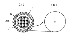
これら結晶成長起因の欠陥を分類すると、成長速度が0.6mm/min前後以上と比較的高速の場合には、空孔タイプの点欠陥が集合したボイド起因とされているFPD、LSTD、COP等のグローンイン欠陥が結晶径方向全域に高密度に存在し、これら欠陥が存在する領域はVリッチ領域と呼ばれている(図5(a)参照)。また、成長速度が0.6mm/min以下の場合は、成長速度の低下に伴い、上記したOSFリングが結晶の周辺から発生し、このリングの外側に転位ループ起因と考えられているL/D(Large Dislocation:格子間転位ループの略号、LSEPD、LFPD等)の欠陥が低密度に存在し、これらの欠陥が存在する領域はIリッチ領域と呼ばれている(図5(b)参照)。さらに、成長速度を0.4mm/min前後と低速にすると、OSFリングがウエーハの中心に凝集して消滅し、全面がIリッチ領域となる(図5(c))。
【0007】
また、最近Vリッチ領域とIリッチ領域の中間でOSFリングの外側に、N領域と呼ばれる、空孔起因のFPD、LSTD、COP等のグローンイン欠陥も、転位ループ起因のLSEPD、LFPDも存在しない領域の存在が発見されている(特開平8−330316号参照)。この領域はOSFリングの外側にあり、そして、酸素析出熱処理を施し、X−ray観察等で析出のコントラストを確認した場合に、酸素析出がほとんどなく、かつ、LSEPD、LFPDが形成されるほどリッチではないIリッチ領域側であると報告している(図4(a)参照)。そして、従来のCZ引上げ機ではウエーハの極一部にしか存在しないN領域を、引上げ機の炉内温度分布を改良し、引上げ速度を調節して、F/G値(単結晶引上げ速度をF[mm/min]とし、シリコンの融点から1300℃の間の引上げ軸方向の結晶内温度勾配の平均値をG[℃/mm]とするとき、F/Gで表わされる比)を0.20〜0.22mm2 /℃・minとしてウエーハ全面及び結晶全長に対して制御すれば、N領域をウエーハ全面に広げることが可能であると提案している(図4(b)参照)。
【0008】
【発明が解決しようとする課題】
しかしながら、このような極低欠陥領域を結晶全体に広げて製造しようとすると、この領域がIリッチ領域側のN領域のみに限定されるため、製造条件の上で制御範囲が極めて狭く、実験機ならともかく生産機では精密制御が難しく、生産性に難点があって実用的でない。
さらに、この発明に開示されていた欠陥分布図は、本発明者らが実験・調査して求めたデータや、データを基にした作成した欠陥分布図(図1参照)とは大幅に異なることが判明した。
【0009】
本発明は、このような問題点に鑑みなされたもので、制御幅が広く、制御し易い製造条件の下で、Vリッチ領域、Iリッチ領域、OSFリングのいずれも存在しない、結晶全面に亙ってN領域で極低欠陥密度であるCZ法によるシリコン単結晶ウエーハを、高生産性を維持しながら得ることを目的とする。
【0010】
【課題を解決するための手段】
本発明は、前記目的を達成するために為されたもので、本発明は、チョクラルスキー法によってシリコン単結晶を育成する際に、引上げ速度をF[mm/min]とし、シリコンの融点から1400℃の間の引上げ軸方向の結晶内温度勾配の平均値をG[℃/mm]で表した時、結晶中心から結晶周辺までの距離D[mm]を横軸とし、F/G[mm2 /℃・min]の値を縦軸として欠陥分布を示した欠陥分布図において、Vリッチ領域とN領域の境界線ならびにN領域とIリッチ領域の境界線で囲繞された領域内で、結晶を引上げ、かつ、結晶中の900℃から600℃までの温度域を通過する時間が700分以下となるように制御することを特徴とするシリコン単結晶の製造方法である。
【0011】
このように、実験・調査の結果を解析して求めた図1の欠陥分布図を基に、Vリッチ領域とN領域の境界線ならびにN領域とIリッチ領域の境界線で囲繞された領域内に収まるように、結晶の引上げ速度Fとシリコンの融点から1400℃の間の引上げ軸方向の結晶内温度勾配の平均値Gを制御して結晶を引上げれば、面内には熱酸化処理をした際にリング状に発生するOSFが存在し、OSFリングの内外が全てN領域である成長単結晶が得られる(図3(b)参照)ことになるが、さらに結晶中の900℃から600℃までの温度域を通過する時間を700分以下となるように熱履歴を制御すれば、OSF核の発生、成長を阻害することができ、ウエーハをOSF熱酸化処理をした際に、OSFリングの核は潜在しているが、OSFリングを発生することはなく、かつウエーハ全面にVリッチ領域、Iリッチ領域も、害を及ぼすようなOSFリングも存在しない全面がN領域である(図3(c)参照)極低欠陥密度なウエーハを得ることができる。
【0012】
そしてこの場合、チョクラルスキー法によってシリコン単結晶を育成する際に、成長結晶中の酸素濃度を24.0ppma以下に制御することが望ましい。
このように、成長結晶中の酸素濃度を24.0ppma(ASTM’79値)以下に制御して引上げれば、OSF核の発生、成長を確実に抑制することができ、OSFリングの潜在核が存在するが、熱酸化処理した際にリング状に発生するOSFは存在しない結晶欠陥の極めて少ないシリコン単結晶ウエーハを得ることができる。
【0013】
本発明は、上記に記載の製造方法により製造されたシリコン単結晶から作製されたシリコン単結晶ウエーハである。本発明で得られるシリコンウエーハは、OSFリングの潜在核が存在し、OSF熱酸化処理をした際にリング状に発生するOSFは存在しない全面がN領域である結晶欠陥の極めて少ないシリコン単結晶ウエーハとなる。
【0014】
そして本発明は、チョクラルスキー法により育成されたシリコン単結晶ウエーハにおいて、単段の熱酸化処理ではOSFは発生しないが、二段の熱酸化処理によりOSFを発生する全面N領域であることを特徴とするシリコン単結晶ウエーハである。
すなわち、本発明のウエーハは、ウエーハ面内にOSFの潜在核はもともと存在するが、通常の一段の熱酸化処理ではOSFは発生せず、二段の熱酸化処理によりOSFの潜在核が成長してOSFを発生する全面N領域である極低欠陥のシリコン単結晶ウエーハである。この二段の熱酸化処理によってのみ発生するOSFは、実際のプロセスでは酸化膜耐圧特性やデバイス特性を悪化させる欠陥にはならない。
【0015】
また、本発明は、酸素析出熱処理により酸素が析出する結晶部分の中に、酸素が析出しない結晶部分が存在するものであることを特徴とするシリコン単結晶ウエーハである。
これは、本発明のウエーハは、OSFの潜在核を有するため、酸素析出熱処理によりOSFリングの潜在核の存在する部分では酸素が析出せず、その周辺で酸素が析出するからである。
【0016】
以下、本発明につき詳細に説明するが、本発明はこれらに限定されるものではない。説明に先立ち各用語につき予め解説しておく。
1)FPD(Flow Pattern Defect)とは、成長後のシリコン単結晶棒からウェーハを切り出し、表面の歪み層を弗酸と硝酸の混合液でエッチングして取り除いた後、K2 Cr2 O7 と弗酸と水の混合液で表面をエッチング(Seccoエッチング)することによりピットおよび流れ模様が生じる。この流れ模様をFPDと称し、ウェーハ面内のFPD密度が高いほど酸化膜耐圧の不良が増える(特開平4−192345号公報参照)。
【0017】
2)SEPD(Secco Etch Pit Defect)とは、FPDと同一のSeccoエッチングを施した時に、流れ模様(flow pattern)を伴うものをFPDと呼び、流れ模様を伴わないものをSEPDと呼ぶ。この中で10μm以上の大きいSEPD(LSEPD)は転位クラスターに起因すると考えられ、デバイスに転位クラスターが存在する場合、この転位を通じて電流がリークし、P−Nジャンクションとしての機能を果たさなくなる。
【0018】
3)LSTD(Laser Scattering Tomography Defect)とは、成長後のシリコン単結晶棒からウエーハを切り出し、表面の歪み層を弗酸と硝酸の混合液でエッチングして取り除いた後、ウエーハを劈開する。この劈開面より赤外光を入射し、ウエーハ表面から出た光を検出することでウエーハ内に存在する欠陥による散乱光を検出することができる。ここで観察される散乱体については学会等ですでに報告があり、酸素析出物とみなされている(J.J.A.P. Vol.32,P3679,1993参照)。また、最近の研究では、八面体のボイド(穴)であるという結果も報告されている。
【0019】
4)COP(Crystal Originated Particle)とは、ウエーハの中心部の酸化膜耐圧を劣化させる原因となる欠陥で、Secco エッチではFPDになる欠陥が、SC−1洗浄(NH4 OH:H2 O2 :H2 O=1:1:10の混合液による洗浄)では選択エッチング液として働き、COPになる。このピットの直径は1μm以下で光散乱法で調べる。
【0020】
5)L/D(Large Dislocation:格子間転位ループの略号)には、LSEPD、LFPD等があり、転位ループ起因と考えられている欠陥である。LSEPDは、上記したようにSEPDの中でも10μm以上の大きいものをいう。また、LFPDは、上記したFPDの中でも先端ピットの大きさが10μm以上の大きいものをいい、こちらも転位ループ起因と考えられている。
【0021】
本発明者らは、先に特願平9−199415号で提案したように、CZ法によるシリコン単結晶成長に関し、V領域とI領域の境界近辺について、詳細に調査したところ、この境界近辺の極く狭い領域にFPD、LSTD、COP等のグローンイン欠陥の数が著しく少なく、LSEPD、LFPD等のL/Dも存在しないニュートラルな領域があることを発見した。
【0022】
そこで、このニュートラルな領域をウエーハ全面に広げることができれば、点欠陥を大幅に減らせると発想し、成長(引上げ)速度と温度勾配の関係の中で、結晶のウエーハ面内では、引上げ速度はほぼ一定であるから、面内の点欠陥の濃度分布を決定する主な因子は温度勾配である。つまり、ウエーハ面内で、軸方向の温度勾配に差があることが問題で、この差を減らすことが出来れば、ウエーハ面内の点欠陥の濃度差も減らせることを見出し、結晶中心部の温度勾配Gcと結晶周辺部分の温度勾配Geとの差を△G=(Ge−Gc)≦5℃/cmとなるように炉内温度を制御して引上げ速度を調節すれば、ウエーハ全面がN領域からなる欠陥のないウエーハが得られるようになった。
【0023】
次いで、特願平9−325428号で提案したように、上記のような温度勾配の差△Gが小さいCZ法による結晶引上げ装置を使用し、引上げ速度を変えて結晶面内を調査した結果、新たに次のような知見を得た。
V−リッチ領域とI−リッチ領域の間に存在するN領域は、従来はOSFリング(核)の外側のみと考えられていたが、OSFリングの内側にも、N領域が存在することを確認した(図3(a)参照)。すなわち、上記特願平9−199415号の場合、OSFリングは、V−リッチ領域とN領域の境界領域となっていた(図4(a)参照)が、この二つは必ずしも一致しないことがわかった。このことは従来の△Gの大きい結晶引上げ装置で実験した場合には発見されず、上記の△Gの小さい結晶引上げ装置を使用した結晶を調査した結果、発見したものである。
【0024】
この調査における引上げ装置の炉内温度を、総合伝熱解析ソフトFEMAG(F.Dupret,P.Nicodeme,Y.Ryckmans,P.Wouters,and M.J.Crochet,Int.J.Heat MassTransfer,33,1849(1990))を使用して鋭意解析を行った。その結果、引上げ速度をF[mm/min]とし、シリコンの融点から1400℃の間の引上げ軸方向の結晶内温度勾配の平均値をG[℃/mm]で表した時、F/Gの値を結晶中心で、0.112〜0.142mm2 /℃・minの範囲内となるように引上げ速度Fと温度勾配平均値Gとを制御すれば、OSF熱酸化処理をした際にリング状に発生するOSFリングあるいはOSFリングの核が存在するものの、グローンイン欠陥及びL/Dがウエーハ全面内に存在しないシリコン単結晶ウエーハが得られることが判った。
【0025】
図1は、直径6インチのシリコン単結晶を例とした場合であるが、結晶の径方向位置を横軸とし、F/G値を縦軸とした場合の諸欠陥分布を表している。図1から明らかなように、OSFリングを含むそのウエーハ内のN領域を最大限に利用するには、結晶中心位置でF/G値を0.112〜0.142mm2 /℃・minとなるようにすればよい。
【0026】
これをウエーハの面で説明すると、従来は、図4(a)に示したように、通常の引上げ速度と結晶引上げ装置におけるOSFリングの外側に存在するN領域を結晶全面に拡大すべく(図4(b)参照)、特別な結晶引上げ装置を用いて引上げ速度と△Gを制御し、無欠陥結晶を製造しようとしていたが、引上げ速度、温度勾配等製造条件の制御幅が極めて狭く、制御が困難で生産性に難点があり、実用的でなかった。
【0027】
そこで、OSFリングの外側のN領域だけに限定せず、OSFリングの内側にも存在するN領域(図3(a)参照)をも使用してN領域を最大限拡大することにした。すなわち、図3(b)に示したようにOSFリングを含んだままN領域を最大限ウエーハ全面に拡大することができる引上げ速度と△G及び結晶引上げ装置を選択して引上げた。その結果、上記したようなF/G値の範囲内に収まるように引上げ速度と結晶内温度勾配を調整して引上げれば、従来よりも拡大された制御幅をもつ製造条件下で容易に低欠陥のウエーハを製造することができる。
【0028】
一方、OSFリングについては、最近の研究からウエーハ全面内で低酸素濃度の場合には、OSFリングの核が存在しても熱酸化処理によりOSFリングを発生することはなく、デバイスに影響を与えないということが判ってきている。
この酸素濃度の限界値は、同一の結晶引上げ装置を使用して、数種類の酸素濃度レベルの結晶を引上げた結果、ウエーハ全面内の酸素濃度が24.0ppma(ASTM’79値)以下であれば、ウエーハの熱酸化処理を行った時にOSFリングが発生しないことが確認されている。
【0029】
すなわち、一本の結晶を引上げ中に徐々に酸素濃度を下げていった時に、結晶全長にわたってOSFとなる核は存在するが、ウエーハの熱酸化処理を行った時にOSFリングが観察されるのは24.0ppmaまでで、24.0ppma以下ではOSFリングの潜在核は存在するが、熱酸化処理によるOSFリングは発生していない。
【0030】
ちなみに、成長結晶中の酸素濃度を24.0ppma以下にするには、従来から一般に用いられている方法で行えばよく、例えば、ルツボの回転数あるいは融液内温度分布等を調整して融液の対流を制御する等の手段により簡単に行うことができる。
【0031】
なお、OSFリングは発生しなくても、その核の存在するところでは酸素析出が少なくなるという傾向があるが、デバイスの低温下プロセスにおいては、強いゲッタリングも要求されないので、OSF領域での酸素析出の少なさは問題にならない。
【0032】
次いでOSFリング核の成長を阻害する結晶成長条件を検討した。炉内温度分布の異なる結晶引上げ装置(炉内構成を変更したもの)を数種類使用して、OSF熱酸化処理時にOSFリングが発生するように、引上げ速度を制御して結晶を引上げた結果、900〜600℃の温度域を645分で通過する熱履歴を与えた結晶には、その後OSFリング発生の有無を確認するOSF熱酸化処理を施してもOSFリングは確認されなかった。
しかしながら、900〜600℃の温度域を770分で通過する熱履歴を与えた結晶には、その後OSFリング発生の有無を確認するOSF熱酸化処理を施したところ、OSFリングが発生した。
【0033】
図2に結晶温度域を100℃毎に区切った時の、その帯域を通過する時間を制御した場合(曲線A)と制御なしで成長させた場合(曲線B)を比較して示した。
図2において、曲線Bの黒丸プロット上の通過時間(三点積算770分)では明らかにOSFリングが発生しており、曲線Aの黒四角プロット上の通過時間(三点積算645分)ではOSFリングの発生はなかった。従って、この900℃から600℃までの温度領域内はOSFリングの潜在核の成長領域と考えられる。従って、この温度帯域をできるだけ短くした方がよい。そして、1100〜900℃の温度域で潜在核が発生するものと考えられている。
【0034】
そこで、F/G値制御による結晶引上げに続いて成長結晶の900℃から600℃までの温度域を通過する熱履歴を700分以下となるように制御してOSFリング核の成長を阻害すれば、OSFの潜在核は存在するが、OSF熱酸化処理をした際にはOSFリングの発生はなく、かつ、グローンイン欠陥及びL/Dが存在せず、結晶全面がN領域で使用可能な領域で占められ、無欠陥の結晶を広い条件範囲で作製することができる。さらに成長結晶中の酸素濃度を24.0ppma以下に抑えれば、OSFリングの発生を確実に抑制することができる。
【0035】
すなわち、CZ法によってシリコン単結晶を育成する際に、引上げ速度をF[mm/min]とし、シリコンの融点から1400℃の間の引上げ軸方向の結晶内温度勾配の平均値をG[℃/mm]で表した時、F/Gの値を結晶中心で、0.112〜0.142mm2 /℃・minに制御し、かつ、前記結晶中の900℃から600℃までの温度域を通過する時間が700分以下となるように制御することによって、全面N領域を持つと共にOSFの潜在核は存在するが、熱酸化処理をしてもOSFリングが発生しない、全面使用可能な無欠陥ウエーハを制御幅の広い条件下で容易に製造することができる。この際、さらに成長結晶中の酸素濃度を24.0ppma以下に制御すれば、OSF潜在核の成長を抑制することができ、OSFリングの発生を確実に抑えることができる。
【0036】
そして、チョクラルスキー法により育成されたシリコン単結晶ウエーハにおいて、例えば、上記のような本発明の製造方法で製造したウエーハは、単段の熱酸化処理ではOSFは発生しないが、二段の熱酸化処理によりOSFを発生する全面N領域から成るシリコン単結晶ウエーハとなる。
ここで、単段の熱酸化処理とは、通常のOSFテストであって、ウエット酸素雰囲気下、昇温して、1150℃で100分間保持した後、降温する方法であり、このテストでOSFが発生する場合は、デバイス特性に悪影響を与えることになる。
また、二段の熱酸化処理とは、特開平6−97251号公報に開示されているシリコン単結晶の品質評価方法であって、一段目は、酸素雰囲気下、1000℃で3時間保持し、続いて二段目ではウエット酸素雰囲気下、1000℃から1150℃に昇温して、1150℃で100分間保持した後、降温する方法である。この方法は、OSF核の存在を明らかにするため、より加速したテストであり、この二段の熱酸化処理によってのみ発生するOSFは、酸化膜耐圧特性やデバイス特性を悪化させる欠陥にはならない。
この二段の強制的な熱酸化処理により発生したOSFの密度は、核の存在を明らかにするため、加速してやっと発生したものであり、通常、デバイス製造においてはこうした条件になることはない。
【0037】
そして、このようなシリコン単結晶ウエーハは、酸素析出熱処理によって酸素が析出する結晶部分の中に、酸素が析出しない結晶部分が存在するというものである。
これは、酸素析出熱処理によりOSFリングの潜在核の存在する部分では酸素が析出し難いためで、その周辺では酸素が析出することになる。
【0038】
【発明の実施の形態】
以下、本発明の実施の形態について、図面を参照しながら詳細に説明する。
まず、本発明で使用するCZ法による単結晶引上げ装置の構成例を図6により説明する。図6に示すように、この単結晶引上げ装置30は、引上げ室31と、引上げ室31中に設けられたルツボ32と、ルツボ32の周囲に配置されたヒータ34と、ルツボ32を回転させるルツボ保持軸33及びその回転機構(図示せず)と、シリコンの種子結晶5を保持するシードチャック6と、シードチャック6を引上げるワイヤ7と、ワイヤ7を回転又は巻き取る巻取機構(図示せず)を備えて構成されている。ルツボ32は、その内側のシリコン融液(湯)2を収容する側には石英ルツボが設けられ、その外側には黒鉛ルツボが設けられている。また、ヒータ34の外側周囲には断熱材35が配置されている。
【0039】
また、本発明の製造方法に関わる製造条件を設定するために、結晶の固液界面の外周に環状の固液界面断熱材8を設け、その上に上部囲繞断熱材9が配置されている。この固液界面断熱材8は、その下端とシリコン融液2の湯面との間に3〜5cmの隙間10を設けて設置されている。上部囲繞断熱材9は条件によっては使用しないこともある。さらに、冷却ガスを吹き付けたり、輻射熱を遮って単結晶を冷却する筒状の冷却装置36を設けてもよい。
別に、最近では引上げ室31の水平方向の外側に、図示しない磁石を設置し、シリコン融液2に水平方向あるいは垂直方向等の磁場を印加することによって、融液の対流を抑制し、単結晶の安定成長をはかる、いわゆるMCZ法が用いられることも多い。
【0040】
次に、上記の単結晶引上げ装置30による単結晶育成方法について説明する。まず、ルツボ32内でシリコンの高純度多結晶原料を融点(約1420°C)以上に加熱して融解する。次に、ワイヤ7を巻き出すことにより融液2の表面略中心部に種結晶5の先端を接触又は浸漬させる。その後、ルツボ保持軸33を適宜の方向に回転させるとともに、ワイヤ7を回転させながら巻き取り種結晶5を引上げることにより、単結晶育成が開始される。以後、引上げ速度と温度を適切に調節することにより略円柱形状の単結晶棒1を得ることができる。
【0041】
この場合、本発明では、温度制御のために特に重要であるのは、図6に示したように、引上げ室31の湯面上の単結晶棒1中の液状部分の外周空間において、湯面近傍の結晶の温度が1420℃から1400℃までの温度域に環状の固液界面断熱材8を設けたことと、その上に上部囲繞断熱材9を配置したことである。さらに、必要に応じてこの断熱材の上部に結晶を冷却する装置、例えば冷却装置36を設けて、これに上部より冷却ガスを吹きつけて結晶を冷却できるものとし、筒下部に輻射熱反射板を取り付けた構造としてもよい。
【0042】
このように液面の直上の位置に所定の隙間を設けて断熱材を配置し、さらにこの断熱材の上部に結晶を冷却する装置を設けた構造とすることによって、結晶成長界面近傍では輻射熱により保温効果が得られ、結晶上部の所定温度帯域では冷却することができるので、本発明の製造条件を満足させることができる。
この結晶の冷却装置としては、前記筒状の冷却装置36とは別に、結晶の周囲を囲繞する空冷ダクトや水冷蛇管等を設けて所望の温度勾配を確保するようにしても良い。
【0043】
【実施例】
以下、本発明の具体的な実施の形態を実施例を挙げて説明するが、本発明はこれらに限定されるものではない。
(実施例1)
図6に示した引上げ装置30で、20インチ石英ルツボに原料多結晶シリコンを60Kgチャージし、直径6インチ、方位<100>のシリコン単結晶棒を平均引上げ速度を0.60mm/minで引上げを行った(単結晶棒の直胴長さ約85cm)。
シリコン融液の湯温は約1420℃、湯面から環状の固液界面断熱材の下端までは、4cmの空間とし、その上に10cm高さの環状固液界面断熱材を配置し、湯面から引上げ室天井までの高さをルツボ保持軸を調整して30cmに設定し、上部囲繞断熱材を配備した。
そして、結晶中心部でのF/G値を0.135mm2 ・℃/minで引上げた。
【0044】
単結晶引上げ中に、図2の曲線A(黒四角プロット)で示したように、結晶中の900〜600℃までの温度域を通過する時間を645分(結晶温度域各100℃当たり通過時間の積算値:900〜800℃/210分、800〜700℃/210分、700〜600℃/225分、計645分)とした熱履歴を与えて引上げ、得られた単結晶棒から、ウエーハを切り出し、鏡面加工を施してシリコン単結晶の鏡面ウエーハを作製し、グローンイン欠陥の測定を行った。また、単段と二段の熱酸化処理を施してOSFリング発生の有無を確認した。
ここで、単段の熱酸化処理とは、通常のOSFテストであって、ウエット酸素雰囲気下、昇温して、1150℃で100分間保持した後、降温する方法であり、このテストでOSFが発生する場合は、デバイス特性に悪影響を与えることになる。
また、二段の熱酸化処理とは、一段目は、酸素雰囲気下、1000℃で3時間保持し、続いて二段目ではウエット酸素雰囲気下、1000℃から1150℃に昇温して、1150℃で100分間保持した後、降温する方法である。
【0045】
その結果、全面グローンイン欠陥の存在しないN領域で、単段の熱酸化処理によっては、OSFリングを発生しない無欠陥ウエーハであった。二段の熱酸化処理によっては、OSFリングが発生したが、この場合のOSFは、デバイス特性に悪影響を及ぼすものではない。
なお、このウエーハの酸化膜耐圧特性は、C−モード良品率100%となった。
ここで、C−モード測定条件は、次の通りである。
1)酸化膜厚:25nm、 2)測定電極:リンドープ・ポリシリコン、
3)電極面積:8mm2 、 4)判定電流:1mA/cm2 、
5)良品判定:絶縁破壊電界が8MV/cm以上のものを良品と判定した。
【0046】
(実施例2)
単結晶引上げ中に成長結晶中の酸素濃度を27.5ppmaから20.0ppmaまで徐々に下げた以外は実施例1と同一条件で引上げ、得られた単結晶棒から、ウエーハを切り出し、鏡面加工を施してシリコン単結晶の鏡面ウエーハを作製し、グローンイン欠陥の測定を行った。また、熱酸化処理を施してOSFリング発生の有無を確認した。
【0047】
その結果、酸素濃度が24.0ppma以上のウエーハであっても、OSF潜在核は存在するが、熱酸化処理時にOSFリングの発生はなく、全面にグローンイン欠陥の存在しないN領域を最大限拡大した極低欠陥ウエーハを得た。なお、このウエーハの酸化膜耐圧特性は、C−モード良品率100%となった。
【0048】
(比較例)
単結晶引上げ中に、図2の曲線B(黒丸プロット)で示したように、結晶中の900〜600℃までの温度域を通過する時間を770分(結晶温度帯各100℃当たり通過時間の積算値:900〜800℃/240分、800〜700℃/250分、700〜600℃/280分、計770分)とした熱履歴を与えた以外は、実施例1と同様の条件で引上げ、得られた単結晶棒から、ウエーハを切り出し、鏡面加工を施してシリコン単結晶の鏡面ウエーハを作製し、グローンイン欠陥の測定を行った。また、熱酸化処理を施してOSFリング発生の有無を確認した。
【0049】
その結果、熱酸化処理によってOSFリングを発生した。OSFリングの内外は、全面グローンイン欠陥の存在しないN領域であった。
【0050】
なお、本発明は、上記実施形態に限定されるものではない。上記実施形態は、例示であり、本発明の特許請求の範囲に記載された技術的思想と実質的に同一な構成を有し、同様な作用効果を奏するものは、いかなるものであっても本発明の技術的範囲に包含される。
【0051】
例えば、上記実施形態においては、直径6インチのシリコン単結晶を育成する場合につき例を挙げて説明したが、本発明はこれには限定されず、直径8〜16インチあるいはそれ以上のシリコン単結晶にも適用できる。
また、本発明は、シリコン融液に水平磁場、縦磁場、カスプ磁場等を印加するいわゆるMCZ法にも適用できることは言うまでもない。
【0052】
【発明の効果】
以上説明したように、本発明によれば、適切なF/G値により単結晶育成条件の制御幅が広くなり、低温域の熱履歴あるいは低酸素化の制御を併用すれば、OSF潜在核は存在するが、熱酸化処理によりOSFリングは発生せず、面内にグローイン欠陥もL/Dも存在しない全面がN領域の無欠陥シリコン単結晶ウエーハを製造することができる。
【図面の簡単な説明】
【図1】シリコン単結晶ウエーハ面内における、結晶の径方向位置を横軸とし、F/G値を縦軸とした場合の諸欠陥分布図である。
【図2】成長結晶の温度域100℃当りの通過時間の変動状況を、実施例1と比較例について表わした説明図である。
【図3】本発明の製造方法における結晶面内諸欠陥分布を説明する説明図である。
(a)通常の引上げ条件で引上げた場合、
(b)V−リッチ領域とI−リッチ領域の間で引上げた場合、
(c)本発明の引上げ条件で引上げた場合。
【図4】従来の引上げ方法における結晶面内諸欠陥分布を表した説明図である。
(a)通常の引上げ条件で引上げた場合、
(b)引上げ速度と結晶内温度勾配を精密制御して引上げた場合。
【図5】従来の引上げ方法における引上げ速度と結晶面内欠陥分布との関係を表した説明図である。
(a)高速引上げの場合、(b)中速引上げの場合、(c)低速引上げの場合。
【図6】本発明で使用したCZ法による単結晶引上げ装置の概略説明図である。
【符号の説明】
1…成長単結晶棒、2…シリコン融液、3…湯面、4…固液界面、
5…種結晶、6…シードチャック、7…ワイヤ、8…固液界面断熱材、
9…上部囲繞断熱材、10…湯面と固液界面断熱材下端との隙間、
30…単結晶引上げ装置、31…引上げ室、32…ルツボ、
33…ルツボ保持軸、34…ヒータ、35…断熱材、36…冷却装置。
V …Vリッチ領域、N…N領域、I…Iリッチ領域、OR…OSFリング。[0001]
TECHNICAL FIELD OF THE INVENTION
The present invention relates to a silicon single crystal wafer having a small number of crystal defects, in particular, a silicon single crystal wafer including an entire N region without an OSF ring, and a method for manufacturing the same.
[0002]
[Prior art]
In recent years, with the miniaturization of elements accompanying the high integration of semiconductor circuits, quality requirements for silicon single crystals produced by the Czochralski method (hereinafter abbreviated as CZ method) as substrates thereof have been increasing. . In particular, there is a defect due to single crystal growth, such as a grown-in defect such as FPD, LSTD, and COP, which deteriorates the withstand voltage characteristic of an oxide film and the characteristics of a device. I have.
[0003]
In describing these defects, first, a vacancy-type point defect called vacancy (hereinafter may be abbreviated as V) incorporated into a silicon single crystal and an interstitial-silicon (Interstitial-Si, hereinafter). The factors that determine the concentration of each of the interstitial silicon point defects, which are sometimes referred to as "I", are generally known.
[0004]
In a silicon single crystal, the V region is a vacancy, that is, a region having many concave portions and holes generated due to a shortage of silicon atoms, and the I region is a dislocation generated due to extra silicon atoms. Neutral (neutral, hereinafter sometimes abbreviated as N) region between the V region and the I region, where there is no shortage or lack of atoms (small). Will exist. The above-mentioned grown-in defects (FPD, LSTD, COP, etc.) are generated only when V and I are supersaturated. It has been found that it does not exist.
[0005]
The concentration of these two-point defects is determined by the relationship between the crystal pulling rate (growth rate) in the CZ method and the temperature gradient G near the solid-liquid interface in the crystal, and the OSF ( It has been confirmed that a defect called an oxidation induced stacking fault (Oxidation Induced Stacking Fault) is distributed in a ring shape (hereinafter sometimes referred to as an OSF ring) when viewed in a cross section perpendicular to the crystal growth axis. Therefore, reduction in the density and size of a defect caused by single crystal growth that deteriorates the withstand voltage characteristic of the oxide film and the characteristics of the device is regarded as important.
[0006]
When these defects caused by crystal growth are classified, when the growth rate is relatively high, about 0.6 mm / min or more, FPD, LSTD, COP, etc., which are considered to be caused by voids in which vacancy-type point defects are gathered. Are present at a high density throughout the crystal diameter direction, and the region where these defects are present is called a V-rich region (see FIG. 5A). When the growth rate is 0.6 mm / min or less, the OSF ring described above is generated from the periphery of the crystal as the growth rate decreases, and the L / D is considered to be caused by dislocation loops outside the ring. (Large Dislocation: abbreviation for interstitial dislocation loop, LSEPD, LFPD, etc.) defects are present at low density, and the region where these defects are present is called an I-rich region (see FIG. 5B). Further, when the growth rate is reduced to about 0.4 mm / min, the OSF ring is agglomerated at the center of the wafer and disappears, and the entire surface becomes an I-rich region (FIG. 5C).
[0007]
In addition, a region called a N region, which is a region between the V-rich region and the I-rich region, which is outside the OSF ring and in which neither a void-based defect such as FPD, LSTD, or COP due to vacancies nor a LSEPD or LFPD due to a dislocation loop exists. Has been found (see JP-A-8-330316). This region is outside the OSF ring, and when oxygen precipitation heat treatment is performed and the contrast of the deposition is confirmed by X-ray observation or the like, there is almost no oxygen precipitation, and the region is rich enough to form LSEPD and LFPD. (See FIG. 4 (a)). Then, in the conventional CZ pulling machine, the N region existing only in a very small part of the wafer is improved by improving the temperature distribution in the furnace of the pulling machine, adjusting the pulling speed, and adjusting the F / G value (the single crystal pulling speed to F [Mm / min], and the average value of the temperature gradient in the crystal in the direction of the pulling axis between the melting point of silicon and 1300 ° C. is G [° C./mm]. ~ 0.22mm 2 It has been proposed that the N region can be extended over the entire surface of the wafer by controlling the entire surface of the wafer and the entire length of the crystal at / ° C. · min (see FIG. 4B).
[0008]
[Problems to be solved by the invention]
However, when such an extremely low defect region is to be manufactured by extending the entire crystal, this region is limited to only the N region on the side of the I-rich region, so that the control range is extremely narrow under the manufacturing conditions. Anyway, precision control is difficult with a production machine, and there is a difficulty in productivity, which is not practical.
Further, the defect distribution diagram disclosed in the present invention is significantly different from the data obtained by experiments and investigations by the present inventors and the defect distribution diagram created based on the data (see FIG. 1). There was found.
[0009]
SUMMARY OF THE INVENTION The present invention has been made in view of the above problems, and has a wide control range, under a manufacturing condition that is easy to control, and over a whole surface of a crystal where neither a V-rich region, an I-rich region, nor an OSF ring exists. Accordingly, it is an object of the present invention to obtain a silicon single crystal wafer by the CZ method having an extremely low defect density in the N region while maintaining high productivity.
[0010]
[Means for Solving the Problems]
The present invention has been made to achieve the above object, and the present invention Is When growing a silicon single crystal by the Czochralski method, the pulling rate is set to F [mm / min], and the average value of the temperature gradient in the crystal in the pulling axis direction from the melting point of silicon to 1400 ° C. is G [° C.]. / Mm], the horizontal axis represents the distance D [mm] from the center of the crystal to the periphery of the crystal, and F / G [mm Two /°C.min] in the defect distribution diagram showing the defect distribution with the ordinate as the vertical axis, the crystal is formed within the region surrounded by the boundary between the V-rich region and the N region and the boundary between the N region and the I-rich region. A method for producing a silicon single crystal, characterized in that the time required for pulling and passing through a temperature range from 900 ° C. to 600 ° C. in the crystal is controlled to be 700 minutes or less.
[0011]
As described above, based on the defect distribution diagram of FIG. 1 obtained by analyzing the results of the experiment and investigation, the region surrounded by the boundary line between the V-rich region and the N region and the boundary line between the N region and the I-rich region When the crystal is pulled by controlling the crystal pulling speed F and the average value G of the temperature gradient in the crystal in the direction of the pulling axis between 1400 ° C. and the melting point of silicon so as to be within the range, the thermal oxidation treatment is performed in the plane. Then, a ring-shaped OSF is present, and a grown single crystal in which the inside and outside of the OSF ring are all N regions is obtained (see FIG. 3B). If the thermal history is controlled so that the time required to pass through the temperature range up to 700 ° C. is 700 minutes or less, the generation and growth of OSF nuclei can be inhibited. When the wafer is subjected to the OSF thermal oxidation treatment, the OSF ring Nucleus is latent, but OSF phosphorus And a V-rich region and an I-rich region on the entire surface of the wafer, and an N region on the entire surface where there is no harmful OSF ring (see FIG. 3C). Can be obtained.
[0012]
And in this case , When growing a silicon single crystal by the Czochralski method, it is desirable to control the oxygen concentration in the grown crystal to 24.0 ppma or less.
As described above, if the oxygen concentration in the grown crystal is controlled to be 24.0 ppma (ASTM '79 value) or less, the generation and growth of the OSF nucleus can be surely suppressed, and the latent nucleus of the OSF ring is reduced. Although it is present, a silicon single crystal wafer having very few crystal defects can be obtained without the presence of OSF generated in a ring shape when subjected to thermal oxidation treatment.
[0013]
The present invention Is , Above It is a silicon single crystal wafer manufactured from the silicon single crystal manufactured by the manufacturing method described. The silicon wafer obtained by the present invention is a silicon single crystal wafer having an extremely small number of crystal defects in which the entire surface is an N region where there is a latent nucleus of an OSF ring and there is no OSF generated in a ring shape during the OSF thermal oxidation treatment. It becomes.
[0014]
And the present invention Is In a silicon single crystal wafer grown by the Czochralski method, an OSF is not generated by a single-stage thermal oxidation process, but is a whole N region where an OSF is generated by a two-stage thermal oxidation process. It is a single crystal wafer.
That is, in the wafer of the present invention, latent OSF nuclei originally exist in the wafer surface, but no OSF is generated by ordinary one-stage thermal oxidation treatment, and latent nuclei of OSF grow by two-stage thermal oxidation treatment. This is an extremely low defect silicon single crystal wafer which is an entire N region where OSF is generated. The OSF generated only by the two-stage thermal oxidation process does not become a defect that deteriorates oxide film breakdown voltage characteristics and device characteristics in an actual process.
[0015]
Also, Book The present invention is a silicon single crystal wafer characterized in that a crystal part where oxygen does not precipitate exists in a crystal part where oxygen is precipitated by the oxygen precipitation heat treatment.
This is because the wafer of the present invention has a latent nucleus of OSF, so that oxygen precipitation heat treatment does not precipitate oxygen in a portion where the latent nucleus of the OSF ring exists, but precipitates oxygen around the portion.
[0016]
Hereinafter, the present invention will be described in detail, but the present invention is not limited thereto. Prior to the explanation, each term will be explained in advance.
1) FPD (Flow Pattern Defect) means that a wafer is cut out from a silicon single crystal rod after growth, and a strained layer on the surface is removed by etching with a mixed solution of hydrofluoric acid and nitric acid. 2 Cr 2 O 7 When the surface is etched (Secco etching) with a mixed solution of water, hydrofluoric acid and water, pits and flow patterns are generated. This flow pattern is called FPD, and the higher the FPD density in the wafer surface, the more the failure of the oxide film breakdown voltage increases (see Japanese Patent Application Laid-Open No. 4-192345).
[0017]
2) SEPD (Secco Etch Pitch Defect) refers to a material with a flow pattern (flow pattern) when subjected to the same Secco etching as the FPD, and a material without a flow pattern is referred to as an SEPD. Among them, a large SEPD (LSEPD) of 10 μm or more is considered to be caused by a dislocation cluster. When a dislocation cluster exists in a device, a current leaks through the dislocation, and the device does not function as a PN junction.
[0018]
3) LSTD (Laser Scattering Tomography Defect) is a method in which a wafer is cut out from a silicon single crystal rod after growth, a strained layer on the surface is removed by etching with a mixed solution of hydrofluoric acid and nitric acid, and then the wafer is cleaved. By irradiating infrared light from this cleavage plane and detecting light emitted from the wafer surface, scattered light due to defects existing in the wafer can be detected. The scatterers observed here have already been reported at academic conferences and the like, and are regarded as oxygen precipitates (see JJAP Vol. 32, P3679, 1993). Recent studies have also reported that it is an octahedral void.
[0019]
4) A COP (Crystal Originated Particle) is a defect that causes deterioration of the oxide film breakdown voltage at the center of the wafer. The defect that becomes an FPD in the Secco etch is SC-1 cleaning (NH 4 OH: H 2 O 2 : H 2 In the case of cleaning with a mixed solution of O = 1: 1: 10), it works as a selective etching solution and becomes COP. The diameter of the pit is 1 μm or less and is examined by a light scattering method.
[0020]
5) L / D (Large Dislocation: abbreviation for interstitial dislocation loop) includes LSEPD, LFPD, and the like, and is a defect considered to be caused by a dislocation loop. LSEPD refers to a large SEPD of 10 μm or more among SEPDs as described above. The LFPD refers to the above-mentioned FPD having a tip pit having a size of 10 μm or more, which is also considered to be caused by a dislocation loop.
[0021]
As previously proposed in Japanese Patent Application No. 9-199415, the present inventors have conducted detailed investigations on the vicinity of the boundary between the V region and the I region with respect to silicon single crystal growth by the CZ method. It has been found that a very small area has a very small number of grown-in defects such as FPD, LSTD and COP, and a neutral area such as LSEPD and LFPD where no L / D exists.
[0022]
The idea is that if this neutral region can be spread over the entire surface of the wafer, point defects can be greatly reduced, and within the relationship between the growth (pulling) speed and the temperature gradient, the pulling speed is within the crystal wafer surface. Since it is almost constant, the main factor that determines the concentration distribution of in-plane point defects is the temperature gradient. In other words, it is a problem that there is a difference in the temperature gradient in the axial direction in the wafer plane, and it is found that if this difference can be reduced, the difference in the concentration of point defects in the wafer plane can also be reduced. If the pulling speed is adjusted by controlling the furnace temperature so that the difference between the temperature gradient Gc and the temperature gradient Ge around the crystal becomes ΔG = (Ge−Gc) ≦ 5 ° C./cm, the entire surface of the wafer becomes N A defect-free wafer consisting of regions can be obtained.
[0023]
Next, as proposed in Japanese Patent Application No. 9-325428, as a result of using a crystal pulling apparatus based on the CZ method with a small difference in temperature gradient ΔG as described above and changing the pulling speed, the in-plane crystal was investigated. The following new knowledge was obtained.
Conventionally, the N region existing between the V-rich region and the I-rich region was considered only outside the OSF ring (nucleus). However, it was confirmed that the N region also exists inside the OSF ring. (See FIG. 3A). That is, in the case of Japanese Patent Application No. 9-199415, the OSF ring is a boundary region between the V-rich region and the N region (see FIG. 4A). all right. This is not found in an experiment with a conventional crystal pulling apparatus having a large ΔG, but was found as a result of investigating crystals using the crystal pulling apparatus having a small ΔG.
[0024]
In this investigation, the furnace temperature of the pulling apparatus was measured using integrated heat transfer analysis software FEMAG (F. Duprep, P. Nicodeme, Y. Ryckmans, P. Wouters, and MJ Crochet, Int. J. Heat Mass Transfer, 33, 1849 (1990)). As a result, when the pulling rate is F [mm / min] and the average value of the temperature gradient in the crystal in the pulling axis direction between the melting point of silicon and 1400 ° C. is represented by G [° C./mm], the F / G The value is 0.112 to 0.142 mm at the crystal center. 2 If the pulling speed F and the average temperature gradient G are controlled so as to be within the range of / ° C. · min, the OSF ring or the nucleus of the OSF ring generated in a ring shape during the OSF thermal oxidation treatment exists. It was found that a silicon single crystal wafer having no grown-in defect and no L / D on the entire surface of the wafer was obtained.
[0025]
FIG. 1 shows a case where a silicon single crystal having a diameter of 6 inches is used as an example, and shows a distribution of various defects when the abscissa represents the radial position of the crystal and the ordinate represents the F / G value. As is apparent from FIG. 1, in order to make the most of the N region in the wafer including the OSF ring, the F / G value should be 0.112 to 0.142 mm at the crystal center position. 2 / ° C. · min.
[0026]
Explaining this in terms of a wafer, conventionally, as shown in FIG. 4A, in order to expand the N region existing outside the OSF ring in the normal pulling speed and crystal pulling apparatus to the entire crystal surface, as shown in FIG. 4 (b)), a defect-free crystal was manufactured by controlling the pulling speed and ΔG using a special crystal pulling apparatus. However, it was not practical due to difficulties in productivity.
[0027]
Therefore, the N region is expanded to the maximum by using not only the N region outside the OSF ring but also the N region (see FIG. 3A) that exists inside the OSF ring. That is, as shown in FIG. 3 (b), the pulling speed, ΔG and crystal pulling device capable of maximizing the N region over the entire surface of the wafer while including the OSF ring were selected and pulled. As a result, if the pulling rate and the temperature gradient in the crystal are adjusted so as to be within the above-mentioned range of the F / G value, the pulling rate can be easily reduced under the manufacturing conditions having a wider control width than before. Defective wafers can be manufactured.
[0028]
On the other hand, in the case of the OSF ring, when the oxygen concentration is low in the entire surface of the wafer from the recent research, the OSF ring is not generated by the thermal oxidation process even if the core of the OSF ring exists, and the device is affected. It turns out that there isn't.
The limit value of this oxygen concentration is determined as follows. As a result of pulling up crystals of several kinds of oxygen concentration levels using the same crystal pulling apparatus, if the oxygen concentration in the entire surface of the wafer is 24.0 ppma (ASTM '79 value) or less. It has been confirmed that the OSF ring does not occur when the wafer is subjected to the thermal oxidation treatment.
[0029]
That is, when the oxygen concentration is gradually lowered while pulling up one crystal, there is a nucleus that becomes OSF over the entire length of the crystal, but the OSF ring is observed when the wafer is subjected to thermal oxidation treatment. At 24.0 ppma or less, at 24.0 ppma or less, latent nuclei of the OSF ring exist, but no OSF ring due to the thermal oxidation treatment occurs.
[0030]
Incidentally, the oxygen concentration in the grown crystal can be reduced to 24.0 ppma or less by a method generally used conventionally, for example, by adjusting the rotation speed of the crucible or the temperature distribution in the melt. Can be easily performed by means such as controlling the convection.
[0031]
Even if the OSF ring does not occur, oxygen precipitation tends to be reduced where the nucleus is present. However, in the low temperature process of the device, strong gettering is not required. Low precipitation does not matter.
[0032]
Next, crystal growth conditions that inhibit the growth of OSF ring nuclei were examined. As a result of using several types of crystal pulling apparatuses (with different furnace configuration) with different temperature distributions in the furnace and controlling the pulling speed to generate an OSF ring during the OSF thermal oxidation treatment, the crystal was pulled. The crystal having a thermal history of passing through the temperature range of -600 ° C for 645 minutes was not subjected to the OSF thermal oxidation treatment for confirming the occurrence of the OSF ring, but the OSF ring was not confirmed.
However, the crystal having a thermal history of passing through a temperature range of 900 to 600 ° C. in 770 minutes was subjected to an OSF thermal oxidation treatment for confirming whether or not an OSF ring was generated. As a result, an OSF ring was generated.
[0033]
FIG. 2 shows a comparison between the case where the time required to pass through the crystal temperature range divided at every 100 ° C. is controlled (curve A) and the case where the growth is performed without control (curve B).
In FIG. 2, the OSF ring is clearly generated at the passage time on the black circle plot of the curve B (770 minutes of three-point integration), and the OSF ring is generated at the passage time on the black square plot of the curve A (645 minutes of three-point integration). No ring occurred. Therefore, the temperature range from 900 ° C. to 600 ° C. is considered to be a growth region for latent nuclei of the OSF ring. Therefore, it is better to make this temperature zone as short as possible. It is considered that latent nuclei are generated in a temperature range of 1100 to 900 ° C.
[0034]
Therefore, following the crystal pulling by controlling the F / G value, the heat history of the grown crystal passing through the temperature range from 900 ° C. to 600 ° C. is controlled to be 700 minutes or less to inhibit the growth of OSF ring nuclei. Although the OSF latent nucleus exists, the OSF ring does not occur when the OSF thermal oxidation treatment is performed, and there is no grown-in defect and L / D. Occupied, defect-free crystals can be produced in a wide range of conditions. Furthermore, if the oxygen concentration in the grown crystal is suppressed to 24.0 ppma or less, the occurrence of the OSF ring can be surely suppressed.
[0035]
That is, when growing a silicon single crystal by the CZ method, the pulling rate is F [mm / min], and the average value of the temperature gradient in the crystal in the pulling axis direction from the melting point of silicon to 1400 ° C. is G [° C. / mm], the value of F / G is 0.112 to 0.142 mm at the center of the crystal. 2 / ° C./min, and by controlling the time required to pass through the temperature range of 900 ° C. to 600 ° C. in the crystal to be 700 minutes or less, to have an N region over the entire surface and a latent nucleus of OSF. Exists, but it is possible to easily manufacture a defect-free wafer that can be used entirely without causing an OSF ring even when subjected to a thermal oxidation treatment under a condition having a wide control width. At this time, if the oxygen concentration in the grown crystal is further controlled to 24.0 ppma or less, the growth of the OSF latent nucleus can be suppressed, and the generation of the OSF ring can be surely suppressed.
[0036]
In a silicon single crystal wafer grown by the Czochralski method, for example, a wafer manufactured by the manufacturing method of the present invention as described above does not generate OSF in a single-stage thermal oxidation treatment, but has a two-stage thermal oxidation process. A silicon single crystal wafer composed of N regions on the entire surface where OSF is generated by the oxidation process.
Here, the single-stage thermal oxidation treatment is a normal OSF test, which is a method of raising the temperature in a wet oxygen atmosphere, maintaining the temperature at 1150 ° C. for 100 minutes, and then lowering the temperature. If it occurs, it will adversely affect device characteristics.
The two-stage thermal oxidation treatment is a method for evaluating the quality of a silicon single crystal disclosed in Japanese Patent Application Laid-Open No. 6-97251, and the first stage is performed by holding at 1000 ° C. for 3 hours in an oxygen atmosphere. Subsequently, in the second stage, the temperature is raised from 1000 ° C. to 1150 ° C. in a wet oxygen atmosphere, kept at 1150 ° C. for 100 minutes, and then lowered. This method is a more accelerated test to clarify the existence of OSF nuclei, and the OSF generated only by this two-stage thermal oxidation treatment does not become a defect that deteriorates oxide film breakdown voltage characteristics and device characteristics.
The density of OSF generated by the two-step forced thermal oxidation treatment is generated only at an accelerated rate to clarify the existence of nuclei, and this condition is not usually satisfied in device manufacture.
[0037]
And in such a silicon single crystal wafer, a crystal part where oxygen does not precipitate exists in a crystal part where oxygen is precipitated by the oxygen precipitation heat treatment.
This is because oxygen hardly precipitates in the portion where the latent nucleus of the OSF ring exists due to the oxygen precipitation heat treatment, and oxygen precipitates around the portion.
[0038]
BEST MODE FOR CARRYING OUT THE INVENTION
Hereinafter, embodiments of the present invention will be described in detail with reference to the drawings.
First, a configuration example of a single crystal pulling apparatus using the CZ method used in the present invention will be described with reference to FIG. As shown in FIG. 6, the single
[0039]
Further, in order to set the manufacturing conditions related to the manufacturing method of the present invention, an annular solid-liquid
Separately, recently, a magnet (not shown) is installed outside the pulling
[0040]
Next, a method for growing a single crystal by the above-described single
[0041]
In this case, in the present invention, what is particularly important for temperature control is that, as shown in FIG. 6, in the outer peripheral space of the liquid portion in the
[0042]
In this way, by providing a predetermined gap at a position immediately above the liquid surface and arranging the heat insulating material, and further by providing a device for cooling the crystal above the heat insulating material, the radiant heat is generated in the vicinity of the crystal growth interface. Since a heat retaining effect is obtained and cooling can be performed in a predetermined temperature zone above the crystal, the production conditions of the present invention can be satisfied.
As a cooling device for the crystal, an air-cooled duct or a water-cooled snake tube surrounding the crystal may be provided separately from the
[0043]
【Example】
Hereinafter, specific embodiments of the present invention will be described with reference to Examples, but the present invention is not limited thereto.
(Example 1)
6 kg of raw material polycrystalline silicon is charged into a 20-inch quartz crucible with a pulling
The temperature of the silicon melt is about 1420 ° C. The space from the surface to the lower end of the ring-shaped solid-liquid interfacial insulation is 4 cm, and a 10 cm-high annular solid-liquid interfacial insulation is placed on top of it. The height from the ceiling to the pulling room ceiling was set to 30 cm by adjusting the crucible holding shaft, and the upper surrounding insulating material was provided.
The F / G value at the center of the crystal is 0.135 mm. 2 -Pulled up at ° C / min.
[0044]
During the pulling of the single crystal, as shown by the curve A (black square plot) in FIG. 2, the time required to pass through the temperature range of 900 to 600 ° C. in the crystal was 645 minutes (the passing time per 100 ° C. for each crystal temperature range). Integrated value: 900 to 800 ° C./210 minutes, 800 to 700 ° C./210 minutes, 700 to 600 ° C./225 minutes, 645 minutes in total), and pulled up. Was cut out and mirror-finished to produce a mirror-finished silicon single crystal wafer, and the measurement of the grown-in defect was performed. In addition, single-stage and two-stage thermal oxidation treatments were performed to check for the occurrence of OSF rings.
Here, the single-stage thermal oxidation treatment is a normal OSF test, which is a method of raising the temperature in a wet oxygen atmosphere, maintaining the temperature at 1150 ° C. for 100 minutes, and then lowering the temperature. If it occurs, it will adversely affect device characteristics.
In the two-stage thermal oxidation treatment, the first stage is performed by holding at 1000 ° C. for 3 hours in an oxygen atmosphere, and then the second stage is performed by increasing the temperature from 1000 ° C. to 1150 ° C. in a wet oxygen atmosphere. This is a method of keeping the temperature at 100 ° C. for 100 minutes and then lowering the temperature.
[0045]
As a result, the wafer was a defect-free wafer in which the OSF ring was not generated by the single-stage thermal oxidation treatment in the N region where there was no grown-in defect. Although the OSF ring is generated by the two-stage thermal oxidation process, the OSF in this case does not adversely affect the device characteristics.
Incidentally, the oxide film breakdown voltage characteristic of this wafer was 100% in the C-mode non-defective rate.
Here, the C-mode measurement conditions are as follows.
1) oxide film thickness: 25 nm, 2) measuring electrode: phosphorus-doped polysilicon,
3) Electrode area: 8 mm 2 4) Judgment current: 1 mA / cm 2 ,
5) Non-defective product: A non-defective product having a dielectric breakdown electric field of 8 MV / cm or more was judged.
[0046]
(Example 2)
Except that the oxygen concentration in the grown crystal was gradually lowered from 27.5 ppma to 20.0 ppma during pulling of the single crystal, the wafer was cut out from the obtained single crystal rod under the same conditions as in Example 1 and mirror-finished. Then, a mirror-finished wafer of silicon single crystal was prepared, and the measurement of a grown-in defect was performed. In addition, thermal oxidation treatment was performed to check for the occurrence of an OSF ring.
[0047]
As a result, even if the wafer had an oxygen concentration of 24.0 ppma or more, latent OSF nuclei were present, but no OSF ring was generated during the thermal oxidation treatment, and the N region in which no grown-in defect was present on the entire surface was maximized. An extremely low defect wafer was obtained. Incidentally, the oxide film breakdown voltage characteristic of this wafer was 100% in the C-mode non-defective rate.
[0048]
(Comparative example)
During the pulling of the single crystal, as shown by a curve B (black circle plot) in FIG. 2, the time required to pass through the temperature range of 900 to 600 ° C. in the crystal was 770 minutes (the passing time per 100 ° C. for each crystal temperature zone). (Integrated value: 900-800 ° C / 240 minutes, 800-700 ° C / 250 minutes, 700-600 ° C / 280 minutes; total 770 minutes) Then, a wafer was cut out from the obtained single crystal rod, mirror-finished, and a silicon single crystal mirror-finished wafer was prepared, and a grown-in defect was measured. In addition, thermal oxidation treatment was performed to check for the occurrence of an OSF ring.
[0049]
As a result, an OSF ring was generated by the thermal oxidation treatment. The inside and outside of the OSF ring were N regions where there was no grown-in defect.
[0050]
Note that the present invention is not limited to the above embodiment. The above-described embodiment is an exemplification, and has substantially the same configuration as the technical idea described in the claims of the present invention, and any device having the same operation and effect can be realized by the present invention. It is included in the technical scope of the invention.
[0051]
For example, in the above embodiment, the case of growing a silicon single crystal having a diameter of 6 inches has been described by way of example. However, the present invention is not limited to this, and a silicon single crystal having a diameter of 8 to 16 inches or more is provided. Also applicable to
Needless to say, the present invention can also be applied to a so-called MCZ method in which a horizontal magnetic field, a vertical magnetic field, a cusp magnetic field, or the like is applied to a silicon melt.
[0052]
【The invention's effect】
As described above, according to the present invention, the control range of the single crystal growing condition is widened by an appropriate F / G value, and the OSF latent nucleus can be controlled by using the heat history in a low temperature region or the control of oxygen reduction. Although it is present, no OSF ring is generated by the thermal oxidation process, and a defect-free silicon single crystal wafer having an entire N region without a glow-in defect or L / D in the surface can be manufactured.
[Brief description of the drawings]
FIG. 1 is a diagram showing various defect distributions in a case where a horizontal axis represents a radial position of a crystal and a vertical axis represents an F / G value in a plane of a silicon single crystal wafer.
FIG. 2 is an explanatory diagram showing a variation of a transit time per 100 ° C. of a temperature range of a grown crystal in Example 1 and Comparative Example.
FIG. 3 is an explanatory view illustrating the distribution of various defects in a crystal plane in the manufacturing method of the present invention.
(A) When raising under normal lifting conditions,
(B) When pulled between the V-rich region and the I-rich region,
(C) When pulled under the pulling conditions of the present invention.
FIG. 4 is an explanatory view showing the distribution of various defects in a crystal plane in a conventional pulling method.
(A) When raising under normal lifting conditions,
(B) The case where the pulling speed and the temperature gradient in the crystal are precisely controlled and pulled.
FIG. 5 is an explanatory diagram showing a relationship between a pulling speed and a defect distribution in a crystal plane in a conventional pulling method.
(A) For high-speed pulling, (b) For medium-speed pulling, and (c) For low-speed pulling.
FIG. 6 is a schematic explanatory view of a single crystal pulling apparatus by a CZ method used in the present invention.
[Explanation of symbols]
1 ... grown single crystal rod, 2 ... silicon melt, 3 ... hot surface, 4 ... solid-liquid interface,
5: seed crystal, 6: seed chuck, 7: wire, 8: solid-liquid interface heat insulator,
9: Upper surrounding insulating material, 10: Gap between the hot water surface and the lower end of the solid-liquid interface insulating material,
30: single crystal pulling apparatus, 31: pulling chamber, 32: crucible,
33: crucible holding shaft, 34: heater, 35: heat insulating material, 36: cooling device.
V: V rich area, N: N area, I: I rich area, OR: OSF ring.
Claims (6)
Priority Applications (6)
| Application Number | Priority Date | Filing Date | Title |
|---|---|---|---|
| JP32930998A JP3601324B2 (en) | 1998-11-19 | 1998-11-19 | Silicon single crystal wafer with few crystal defects and method of manufacturing the same |
| PCT/JP1999/006287 WO2000031324A1 (en) | 1998-11-19 | 1999-11-11 | Single-crystal silicon wafer having few crystal defects and method for manufacturing the same |
| US09/600,033 US6334896B1 (en) | 1998-11-19 | 1999-11-11 | Single-crystal silicon wafer having few crystal defects and method for manufacturing the same |
| DE69939376T DE69939376D1 (en) | 1998-11-19 | 1999-11-11 | CRYSTAL SILICON WAFERS WITH LITTLE CRYSTAL DEFECTS AND METHOD FOR THE PRODUCTION THEREOF |
| EP99972699A EP1074643B1 (en) | 1998-11-19 | 1999-11-11 | Single-crystal silicon wafer having few crystal defects and method for manufacturing the same |
| KR1020007007897A KR100725671B1 (en) | 1998-11-19 | 1999-11-11 | Silicon single crystal wafer with less crystal defect and manufacturing method thereof |
Applications Claiming Priority (1)
| Application Number | Priority Date | Filing Date | Title |
|---|---|---|---|
| JP32930998A JP3601324B2 (en) | 1998-11-19 | 1998-11-19 | Silicon single crystal wafer with few crystal defects and method of manufacturing the same |
Publications (2)
| Publication Number | Publication Date |
|---|---|
| JP2000154093A JP2000154093A (en) | 2000-06-06 |
| JP3601324B2 true JP3601324B2 (en) | 2004-12-15 |
Family
ID=18220028
Family Applications (1)
| Application Number | Title | Priority Date | Filing Date |
|---|---|---|---|
| JP32930998A Expired - Fee Related JP3601324B2 (en) | 1998-11-19 | 1998-11-19 | Silicon single crystal wafer with few crystal defects and method of manufacturing the same |
Country Status (6)
| Country | Link |
|---|---|
| US (1) | US6334896B1 (en) |
| EP (1) | EP1074643B1 (en) |
| JP (1) | JP3601324B2 (en) |
| KR (1) | KR100725671B1 (en) |
| DE (1) | DE69939376D1 (en) |
| WO (1) | WO2000031324A1 (en) |
Families Citing this family (17)
| Publication number | Priority date | Publication date | Assignee | Title |
|---|---|---|---|---|
| JP3943717B2 (en) * | 1998-06-11 | 2007-07-11 | 信越半導体株式会社 | Silicon single crystal wafer and manufacturing method thereof |
| KR100622884B1 (en) * | 1998-10-14 | 2006-09-12 | 엠이엠씨 일렉트로닉 머티리얼즈 인코포레이티드 | Thermally Annealed Low Defect Density Monocrystalline Silicon |
| TW593798B (en) * | 1998-11-20 | 2004-06-21 | Komatsu Denshi Kinzoku Kk | Production of silicon single crystal wafer |
| JP3601340B2 (en) * | 1999-02-01 | 2004-12-15 | 信越半導体株式会社 | Epitaxial silicon wafer, method for manufacturing the same, and substrate for epitaxial silicon wafer |
| JP2001068420A (en) * | 1999-08-30 | 2001-03-16 | Komatsu Electronic Metals Co Ltd | Manufacture of epitaxial silicon wafer |
| DE60144416D1 (en) * | 2000-01-25 | 2011-05-26 | Shinetsu Handotai Kk | METHOD FOR DETERMINING UNDER THE CONDITIONS OF THE SILICON INCREDIENT MADE AND METHOD FOR PRODUCING THE SILICON WAFERS |
| JP4092946B2 (en) | 2002-05-09 | 2008-05-28 | 信越半導体株式会社 | Silicon single crystal wafer, epitaxial wafer, and method for producing silicon single crystal |
| CN100472001C (en) * | 2003-02-25 | 2009-03-25 | 株式会社上睦可 | Silicon wafer, process for producing the same and method of growing silicon single crystal |
| JP4151474B2 (en) * | 2003-05-13 | 2008-09-17 | 信越半導体株式会社 | Method for producing single crystal and single crystal |
| US7326395B2 (en) * | 2003-08-20 | 2008-02-05 | Shin-Etsu Handotai Co., Ltd. | Method for producing a single crystal and silicon single crystal wafer |
| JP4483729B2 (en) | 2005-07-25 | 2010-06-16 | 株式会社Sumco | Silicon single crystal manufacturing method |
| JP4853237B2 (en) * | 2006-11-06 | 2012-01-11 | 株式会社Sumco | Epitaxial wafer manufacturing method |
| JP6052189B2 (en) * | 2014-01-16 | 2016-12-27 | 信越半導体株式会社 | Heat treatment method for silicon single crystal wafer |
| EP3953504B1 (en) | 2019-04-11 | 2023-07-12 | GlobalWafers Co., Ltd. | Process for preparing ingot having reduced distortion at late body length |
| JP2022529451A (en) | 2019-04-18 | 2022-06-22 | グローバルウェーハズ カンパニー リミテッド | Growth method of single crystal silicon ingot using continuous Czochralski method |
| US11111596B2 (en) | 2019-09-13 | 2021-09-07 | Globalwafers Co., Ltd. | Single crystal silicon ingot having axial uniformity |
| US11111597B2 (en) | 2019-09-13 | 2021-09-07 | Globalwafers Co., Ltd. | Methods for growing a nitrogen doped single crystal silicon ingot using continuous Czochralski method |
Family Cites Families (7)
| Publication number | Priority date | Publication date | Assignee | Title |
|---|---|---|---|---|
| JP2758093B2 (en) * | 1991-10-07 | 1998-05-25 | 信越半導体株式会社 | Manufacturing method of semiconductor wafer |
| JP3274246B2 (en) * | 1993-08-23 | 2002-04-15 | コマツ電子金属株式会社 | Manufacturing method of epitaxial wafer |
| JP3085146B2 (en) * | 1995-05-31 | 2000-09-04 | 住友金属工業株式会社 | Silicon single crystal wafer and method of manufacturing the same |
| DE69806369T2 (en) * | 1997-04-09 | 2003-07-10 | Memc Electronic Materials, Inc. | LOW ERROR-TIGHT SILICUM AND IDEAL OXYGEN DEPTH |
| JP3460551B2 (en) | 1997-11-11 | 2003-10-27 | 信越半導体株式会社 | Silicon single crystal wafer with few crystal defects and method of manufacturing the same |
| US6077343A (en) * | 1998-06-04 | 2000-06-20 | Shin-Etsu Handotai Co., Ltd. | Silicon single crystal wafer having few defects wherein nitrogen is doped and a method for producing it |
| JP3943717B2 (en) * | 1998-06-11 | 2007-07-11 | 信越半導体株式会社 | Silicon single crystal wafer and manufacturing method thereof |
-
1998
- 1998-11-19 JP JP32930998A patent/JP3601324B2/en not_active Expired - Fee Related
-
1999
- 1999-11-11 WO PCT/JP1999/006287 patent/WO2000031324A1/en active IP Right Grant
- 1999-11-11 DE DE69939376T patent/DE69939376D1/en not_active Expired - Lifetime
- 1999-11-11 KR KR1020007007897A patent/KR100725671B1/en not_active IP Right Cessation
- 1999-11-11 EP EP99972699A patent/EP1074643B1/en not_active Expired - Lifetime
- 1999-11-11 US US09/600,033 patent/US6334896B1/en not_active Expired - Lifetime
Also Published As
| Publication number | Publication date |
|---|---|
| EP1074643A4 (en) | 2006-04-12 |
| DE69939376D1 (en) | 2008-10-02 |
| EP1074643B1 (en) | 2008-08-20 |
| EP1074643A1 (en) | 2001-02-07 |
| KR100725671B1 (en) | 2007-06-08 |
| WO2000031324A1 (en) | 2000-06-02 |
| US6334896B1 (en) | 2002-01-01 |
| JP2000154093A (en) | 2000-06-06 |
| KR20010034231A (en) | 2001-04-25 |
Similar Documents
| Publication | Publication Date | Title |
|---|---|---|
| JP3747123B2 (en) | Method for producing silicon single crystal with few crystal defects and silicon single crystal wafer | |
| JP3943717B2 (en) | Silicon single crystal wafer and manufacturing method thereof | |
| JP3460551B2 (en) | Silicon single crystal wafer with few crystal defects and method of manufacturing the same | |
| JP3994665B2 (en) | Silicon single crystal wafer and method for producing silicon single crystal | |
| EP0890662B1 (en) | Method and apparatus for manufacturing a silicon single crystal having few crystal defects, and a silicon single crystal and silicon wafers manufactured by the same | |
| US6893499B2 (en) | Silicon single crystal wafer and method for manufacturing the same | |
| JP3601324B2 (en) | Silicon single crystal wafer with few crystal defects and method of manufacturing the same | |
| JP3692812B2 (en) | Nitrogen-doped low-defect silicon single crystal wafer and manufacturing method thereof | |
| JP3919308B2 (en) | Method for producing silicon single crystal with few crystal defects and silicon single crystal and silicon wafer produced by this method | |
| JP4020987B2 (en) | Silicon single crystal having no crystal defects around the wafer and its manufacturing method | |
| JP4699675B2 (en) | Annealed wafer manufacturing method | |
| JP3627498B2 (en) | Method for producing silicon single crystal | |
| EP1502972B1 (en) | A silicon single crystal wafer, an epitaxial wafer and method for producing silicon single crystal | |
| JP3634133B2 (en) | Method for producing silicon single crystal with few crystal defects and silicon single crystal wafer | |
| JP4218080B2 (en) | Silicon single crystal wafer and manufacturing method thereof | |
| JPH11349394A (en) | Nitrogen-doped silicon single crystal wafer having low defect density and it production | |
| JP2005119964A (en) | Nitrogen-doped silicon single crystal wafer having few defects and method for producing the same |
Legal Events
| Date | Code | Title | Description |
|---|---|---|---|
| A131 | Notification of reasons for refusal |
Free format text: JAPANESE INTERMEDIATE CODE: A131 Effective date: 20040106 |
|
| A521 | Request for written amendment filed |
Free format text: JAPANESE INTERMEDIATE CODE: A523 Effective date: 20040305 |
|
| A131 | Notification of reasons for refusal |
Free format text: JAPANESE INTERMEDIATE CODE: A131 Effective date: 20040518 |
|
| A521 | Request for written amendment filed |
Free format text: JAPANESE INTERMEDIATE CODE: A523 Effective date: 20040720 |
|
| TRDD | Decision of grant or rejection written | ||
| A01 | Written decision to grant a patent or to grant a registration (utility model) |
Free format text: JAPANESE INTERMEDIATE CODE: A01 Effective date: 20040831 |
|
| A61 | First payment of annual fees (during grant procedure) |
Free format text: JAPANESE INTERMEDIATE CODE: A61 Effective date: 20040913 |
|
| R150 | Certificate of patent or registration of utility model |
Free format text: JAPANESE INTERMEDIATE CODE: R150 |
|
| FPAY | Renewal fee payment (event date is renewal date of database) |
Free format text: PAYMENT UNTIL: 20071001 Year of fee payment: 3 |
|
| FPAY | Renewal fee payment (event date is renewal date of database) |
Free format text: PAYMENT UNTIL: 20081001 Year of fee payment: 4 |
|
| FPAY | Renewal fee payment (event date is renewal date of database) |
Free format text: PAYMENT UNTIL: 20081001 Year of fee payment: 4 |
|
| S531 | Written request for registration of change of domicile |
Free format text: JAPANESE INTERMEDIATE CODE: R313531 |
|
| FPAY | Renewal fee payment (event date is renewal date of database) |
Free format text: PAYMENT UNTIL: 20081001 Year of fee payment: 4 |
|
| R350 | Written notification of registration of transfer |
Free format text: JAPANESE INTERMEDIATE CODE: R350 |
|
| FPAY | Renewal fee payment (event date is renewal date of database) |
Free format text: PAYMENT UNTIL: 20091001 Year of fee payment: 5 |
|
| FPAY | Renewal fee payment (event date is renewal date of database) |
Free format text: PAYMENT UNTIL: 20101001 Year of fee payment: 6 |
|
| FPAY | Renewal fee payment (event date is renewal date of database) |
Free format text: PAYMENT UNTIL: 20111001 Year of fee payment: 7 |
|
| FPAY | Renewal fee payment (event date is renewal date of database) |
Free format text: PAYMENT UNTIL: 20121001 Year of fee payment: 8 |
|
| FPAY | Renewal fee payment (event date is renewal date of database) |
Free format text: PAYMENT UNTIL: 20131001 Year of fee payment: 9 |
|
| R250 | Receipt of annual fees |
Free format text: JAPANESE INTERMEDIATE CODE: R250 |
|
| R250 | Receipt of annual fees |
Free format text: JAPANESE INTERMEDIATE CODE: R250 |
|
| R250 | Receipt of annual fees |
Free format text: JAPANESE INTERMEDIATE CODE: R250 |
|
| S531 | Written request for registration of change of domicile |
Free format text: JAPANESE INTERMEDIATE CODE: R313531 |
|
| R350 | Written notification of registration of transfer |
Free format text: JAPANESE INTERMEDIATE CODE: R350 |
|
| R250 | Receipt of annual fees |
Free format text: JAPANESE INTERMEDIATE CODE: R250 |
|
| R250 | Receipt of annual fees |
Free format text: JAPANESE INTERMEDIATE CODE: R250 |
|
| LAPS | Cancellation because of no payment of annual fees |