JP2020202010A - Connector device - Google Patents
Connector device Download PDFInfo
- Publication number
- JP2020202010A JP2020202010A JP2019105729A JP2019105729A JP2020202010A JP 2020202010 A JP2020202010 A JP 2020202010A JP 2019105729 A JP2019105729 A JP 2019105729A JP 2019105729 A JP2019105729 A JP 2019105729A JP 2020202010 A JP2020202010 A JP 2020202010A
- Authority
- JP
- Japan
- Prior art keywords
- housing
- mold resin
- resin portion
- connector
- connector device
- Prior art date
- Legal status (The legal status is an assumption and is not a legal conclusion. Google has not performed a legal analysis and makes no representation as to the accuracy of the status listed.)
- Pending
Links
- 239000011347 resin Substances 0.000 claims abstract description 126
- 229920005989 resin Polymers 0.000 claims abstract description 126
- 239000000463 material Substances 0.000 claims abstract description 60
- 239000004020 conductor Substances 0.000 claims abstract description 36
- 239000000470 constituent Substances 0.000 claims abstract description 34
- 238000003466 welding Methods 0.000 claims abstract description 18
- 238000012360 testing method Methods 0.000 claims description 50
- 238000002834 transmittance Methods 0.000 claims description 34
- 229920000728 polyester Polymers 0.000 claims description 18
- 238000002347 injection Methods 0.000 claims description 10
- 239000007924 injection Substances 0.000 claims description 10
- 229920006122 polyamide resin Polymers 0.000 claims description 7
- 238000004519 manufacturing process Methods 0.000 abstract description 6
- 238000010586 diagram Methods 0.000 abstract 1
- XLYOFNOQVPJJNP-UHFFFAOYSA-N water Substances O XLYOFNOQVPJJNP-UHFFFAOYSA-N 0.000 description 17
- 238000001746 injection moulding Methods 0.000 description 13
- 230000002093 peripheral effect Effects 0.000 description 12
- 238000000465 moulding Methods 0.000 description 11
- 239000000853 adhesive Substances 0.000 description 9
- 230000001070 adhesive effect Effects 0.000 description 9
- 239000003566 sealing material Substances 0.000 description 9
- 239000007788 liquid Substances 0.000 description 6
- 230000015572 biosynthetic process Effects 0.000 description 5
- 239000003086 colorant Substances 0.000 description 5
- 230000013011 mating Effects 0.000 description 5
- 238000005266 casting Methods 0.000 description 4
- 230000006378 damage Effects 0.000 description 4
- 238000011156 evaluation Methods 0.000 description 4
- 229920001707 polybutylene terephthalate Polymers 0.000 description 4
- 238000010292 electrical insulation Methods 0.000 description 3
- 229910000679 solder Inorganic materials 0.000 description 3
- 238000009864 tensile test Methods 0.000 description 3
- 239000004952 Polyamide Substances 0.000 description 2
- 239000006229 carbon black Substances 0.000 description 2
- 238000005520 cutting process Methods 0.000 description 2
- 230000000694 effects Effects 0.000 description 2
- 239000000446 fuel Substances 0.000 description 2
- 230000001678 irradiating effect Effects 0.000 description 2
- 238000005259 measurement Methods 0.000 description 2
- 239000000155 melt Substances 0.000 description 2
- 238000002844 melting Methods 0.000 description 2
- 230000008018 melting Effects 0.000 description 2
- 229920002647 polyamide Polymers 0.000 description 2
- 238000002360 preparation method Methods 0.000 description 2
- 238000003825 pressing Methods 0.000 description 2
- 239000004065 semiconductor Substances 0.000 description 2
- 229920006346 thermoplastic polyester elastomer Polymers 0.000 description 2
- 238000010521 absorption reaction Methods 0.000 description 1
- 229920001971 elastomer Polymers 0.000 description 1
- 239000000806 elastomer Substances 0.000 description 1
- 239000000835 fiber Substances 0.000 description 1
- 230000008595 infiltration Effects 0.000 description 1
- 238000001764 infiltration Methods 0.000 description 1
- 238000003780 insertion Methods 0.000 description 1
- 230000037431 insertion Effects 0.000 description 1
- 239000002184 metal Substances 0.000 description 1
- 238000000034 method Methods 0.000 description 1
- 238000012986 modification Methods 0.000 description 1
- 230000004048 modification Effects 0.000 description 1
- 230000000149 penetrating effect Effects 0.000 description 1
- -1 polybutylene terephthalate Polymers 0.000 description 1
- 238000010008 shearing Methods 0.000 description 1
- 229920001169 thermoplastic Polymers 0.000 description 1
- 239000004416 thermosoftening plastic Substances 0.000 description 1
Images


Classifications
-
- H—ELECTRICITY
- H01—ELECTRIC ELEMENTS
- H01R—ELECTRICALLY-CONDUCTIVE CONNECTIONS; STRUCTURAL ASSOCIATIONS OF A PLURALITY OF MUTUALLY-INSULATED ELECTRICAL CONNECTING ELEMENTS; COUPLING DEVICES; CURRENT COLLECTORS
- H01R12/00—Structural associations of a plurality of mutually-insulated electrical connecting elements, specially adapted for printed circuits, e.g. printed circuit boards [PCB], flat or ribbon cables, or like generally planar structures, e.g. terminal strips, terminal blocks; Coupling devices specially adapted for printed circuits, flat or ribbon cables, or like generally planar structures; Terminals specially adapted for contact with, or insertion into, printed circuits, flat or ribbon cables, or like generally planar structures
- H01R12/70—Coupling devices
- H01R12/71—Coupling devices for rigid printing circuits or like structures
- H01R12/72—Coupling devices for rigid printing circuits or like structures coupling with the edge of the rigid printed circuits or like structures
- H01R12/722—Coupling devices for rigid printing circuits or like structures coupling with the edge of the rigid printed circuits or like structures coupling devices mounted on the edge of the printed circuits
- H01R12/724—Coupling devices for rigid printing circuits or like structures coupling with the edge of the rigid printed circuits or like structures coupling devices mounted on the edge of the printed circuits containing contact members forming a right angle
-
- H—ELECTRICITY
- H01—ELECTRIC ELEMENTS
- H01R—ELECTRICALLY-CONDUCTIVE CONNECTIONS; STRUCTURAL ASSOCIATIONS OF A PLURALITY OF MUTUALLY-INSULATED ELECTRICAL CONNECTING ELEMENTS; COUPLING DEVICES; CURRENT COLLECTORS
- H01R12/00—Structural associations of a plurality of mutually-insulated electrical connecting elements, specially adapted for printed circuits, e.g. printed circuit boards [PCB], flat or ribbon cables, or like generally planar structures, e.g. terminal strips, terminal blocks; Coupling devices specially adapted for printed circuits, flat or ribbon cables, or like generally planar structures; Terminals specially adapted for contact with, or insertion into, printed circuits, flat or ribbon cables, or like generally planar structures
- H01R12/50—Fixed connections
- H01R12/51—Fixed connections for rigid printed circuits or like structures
-
- H—ELECTRICITY
- H01—ELECTRIC ELEMENTS
- H01R—ELECTRICALLY-CONDUCTIVE CONNECTIONS; STRUCTURAL ASSOCIATIONS OF A PLURALITY OF MUTUALLY-INSULATED ELECTRICAL CONNECTING ELEMENTS; COUPLING DEVICES; CURRENT COLLECTORS
- H01R13/00—Details of coupling devices of the kinds covered by groups H01R12/70 or H01R24/00 - H01R33/00
- H01R13/46—Bases; Cases
- H01R13/52—Dustproof, splashproof, drip-proof, waterproof, or flameproof cases
- H01R13/5216—Dustproof, splashproof, drip-proof, waterproof, or flameproof cases characterised by the sealing material, e.g. gels or resins
-
- H—ELECTRICITY
- H01—ELECTRIC ELEMENTS
- H01R—ELECTRICALLY-CONDUCTIVE CONNECTIONS; STRUCTURAL ASSOCIATIONS OF A PLURALITY OF MUTUALLY-INSULATED ELECTRICAL CONNECTING ELEMENTS; COUPLING DEVICES; CURRENT COLLECTORS
- H01R13/00—Details of coupling devices of the kinds covered by groups H01R12/70 or H01R24/00 - H01R33/00
- H01R13/46—Bases; Cases
- H01R13/52—Dustproof, splashproof, drip-proof, waterproof, or flameproof cases
- H01R13/5219—Sealing means between coupling parts, e.g. interfacial seal
-
- H—ELECTRICITY
- H05—ELECTRIC TECHNIQUES NOT OTHERWISE PROVIDED FOR
- H05K—PRINTED CIRCUITS; CASINGS OR CONSTRUCTIONAL DETAILS OF ELECTRIC APPARATUS; MANUFACTURE OF ASSEMBLAGES OF ELECTRICAL COMPONENTS
- H05K1/00—Printed circuits
- H05K1/18—Printed circuits structurally associated with non-printed electric components
- H05K1/181—Printed circuits structurally associated with non-printed electric components associated with surface mounted components
-
- H—ELECTRICITY
- H01—ELECTRIC ELEMENTS
- H01R—ELECTRICALLY-CONDUCTIVE CONNECTIONS; STRUCTURAL ASSOCIATIONS OF A PLURALITY OF MUTUALLY-INSULATED ELECTRICAL CONNECTING ELEMENTS; COUPLING DEVICES; CURRENT COLLECTORS
- H01R4/00—Electrically-conductive connections between two or more conductive members in direct contact, i.e. touching one another; Means for effecting or maintaining such contact; Electrically-conductive connections having two or more spaced connecting locations for conductors and using contact members penetrating insulation
- H01R4/02—Soldered or welded connections
- H01R4/029—Welded connections
-
- H—ELECTRICITY
- H01—ELECTRIC ELEMENTS
- H01R—ELECTRICALLY-CONDUCTIVE CONNECTIONS; STRUCTURAL ASSOCIATIONS OF A PLURALITY OF MUTUALLY-INSULATED ELECTRICAL CONNECTING ELEMENTS; COUPLING DEVICES; CURRENT COLLECTORS
- H01R43/00—Apparatus or processes specially adapted for manufacturing, assembling, maintaining, or repairing of line connectors or current collectors or for joining electric conductors
- H01R43/02—Apparatus or processes specially adapted for manufacturing, assembling, maintaining, or repairing of line connectors or current collectors or for joining electric conductors for soldered or welded connections
- H01R43/0221—Laser welding
Landscapes
- Engineering & Computer Science (AREA)
- Microelectronics & Electronic Packaging (AREA)
- Chemical & Material Sciences (AREA)
- Dispersion Chemistry (AREA)
- Connector Housings Or Holding Contact Members (AREA)
- Casings For Electric Apparatus (AREA)
- Coupling Device And Connection With Printed Circuit (AREA)
Abstract
【課題】小型で製造し易い上に、防水性能に優れるコネクタ装置を提供する。【解決手段】回路基板と、コネクタと、モールド樹脂部とを備え、前記回路基板は、導体路を有し、前記コネクタは、樹脂を含むハウジングと、前記ハウジングから突出して前記導体路に接続される端子とを有し、前記モールド樹脂部は、前記導体路と、前記ハウジングから突出された端子と、前記ハウジングの一部とをまとめて覆い、前記ハウジングと前記モールド樹脂部とは、互いの構成材料が溶着されてなる溶着部を有する、コネクタ装置。【選択図】図1PROBLEM TO BE SOLVED: To provide a connector device which is small in size, easy to manufacture, and has excellent waterproof performance. A circuit board, a connector, and a molded resin portion are provided, the circuit board has a conductor path, and the connector is connected to a housing containing resin and projecting from the housing to the conductor path. The mold resin portion covers the conductor path, the terminal protruding from the housing, and a part of the housing together, and the housing and the mold resin portion are mutually covered. A connector device having a welded portion formed by welding a constituent material. [Selection diagram] Fig. 1
Description
本開示は、コネクタ装置に関する。 The present disclosure relates to a connector device.
特許文献1には、回路基板とコネクタと筐体とシール材とを備える電子装置(コネクタ装置)が開示されている。回路基板の全体とコネクタの一部とが筐体内に収納されている。筐体は、上面が開口する箱状のケースと、ケースの上面開口部を閉鎖するカバーとを備える。シール材は、筐体のケースとカバーとの間に介在されている。
上述のコネクタ装置は、筐体を備えることで大型化する。また、筐体のケースとカバーとの間に別途シール材を介在させるため、部品点数が多く製造作業が煩雑になり易い。 The connector device described above is increased in size by including a housing. Further, since a sealing material is separately interposed between the case and the cover of the housing, the number of parts is large and the manufacturing work tends to be complicated.
そこで、本開示は、小型で製造し易い上に、防水性能に優れるコネクタ装置を提供することを目的の一つとする。 Therefore, one of the purposes of the present disclosure is to provide a connector device which is small in size, easy to manufacture, and has excellent waterproof performance.
本開示に係るコネクタ装置は、
回路基板と、
コネクタと、
モールド樹脂部とを備え、
前記回路基板は、導体路を有し、
前記コネクタは、
樹脂を含むハウジングと、
前記ハウジングから突出して前記導体路に接続される端子とを有し、
前記モールド樹脂部は、前記導体路と、前記ハウジングから突出された端子と、前記ハウジングの一部とをまとめて覆い、
前記ハウジングと前記モールド樹脂部とは、互いの構成材料が溶着されてなる溶着部を有する。
The connector device according to the present disclosure is
With the circuit board
With the connector
Equipped with a mold resin part,
The circuit board has a conductor path and has a conductor path.
The connector is
With a housing containing resin
It has a terminal that protrudes from the housing and is connected to the conductor path.
The mold resin portion collectively covers the conductor path, the terminal protruding from the housing, and a part of the housing.
The housing and the mold resin portion have a welded portion formed by welding each other's constituent materials.
本開示に係るコネクタ装置は、小型で製造し易い上に、防水性能に優れる。 The connector device according to the present disclosure is small in size, easy to manufacture, and has excellent waterproof performance.
《本開示の実施形態の説明》
最初に本開示の実施態様を列記して説明する。
<< Explanation of Embodiments of the present disclosure >>
First, embodiments of the present disclosure will be listed and described.
(1)本開示の一態様に係るコネクタ装置は、
回路基板と、
コネクタと、
モールド樹脂部とを備え、
前記回路基板は、導体路を有し、
前記コネクタは、
樹脂を含むハウジングと、
前記ハウジングから突出して前記導体路に接続される端子とを有し、
前記モールド樹脂部は、前記導体路と、前記ハウジングから突出された端子と、前記ハウジングの一部とをまとめて覆い、
前記ハウジングと前記モールド樹脂部とは、互いの構成材料が溶着されてなる溶着部を有する。
(1) The connector device according to one aspect of the present disclosure is
With the circuit board
With the connector
Equipped with a mold resin part,
The circuit board has a conductor path and has a conductor path.
The connector is
With a housing containing resin
It has a terminal that protrudes from the housing and is connected to the conductor path.
The mold resin portion collectively covers the conductor path, the terminal protruding from the housing, and a part of the housing.
The housing and the mold resin portion have a welded portion formed by welding each other's constituent materials.
上記の構成は、防水性能に優れる。コネクタのハウジングとモールド樹脂部とが溶着部を有することで、ハウジングとモールド樹脂部との密着性が高いからである。そのため、ハウジングとモールド樹脂部との隙間から水などの液体の浸入を抑制し易い。よって、モールド樹脂部で覆われる導体路やコネクタの端子などの導電部材に液体が付着することを抑制できる。 The above configuration is excellent in waterproof performance. This is because the housing of the connector and the mold resin portion have a welded portion, so that the housing and the mold resin portion have high adhesion. Therefore, it is easy to suppress the intrusion of liquid such as water from the gap between the housing and the mold resin portion. Therefore, it is possible to prevent the liquid from adhering to the conductive member such as the conductor path covered with the mold resin portion and the terminal of the connector.
また、上記の構成は、小型化し易い。モールド樹脂部が回路基板などをまとめて覆っていることで、回路基板などを収納する筐体(ケースとカバー)を別途備えなくてもよいからである。 Further, the above configuration is easy to miniaturize. This is because the mold resin portion covers the circuit board and the like together, so that it is not necessary to separately provide a housing (case and cover) for accommodating the circuit board and the like.
更に、上記の構成は、製造し易い。上記筐体とシール材とが不要なため、部品点数が少ないからである。その上、筐体にシール材を配置する作業や筐体を組み立てる作業が不要だからである。筐体が不要なのは、上述したようにモールド樹脂部で回路基板などをまとめて覆っているからである。シール材が不要なのは、上述したように溶着部により十分な防水性能を備えているからである。 Further, the above configuration is easy to manufacture. This is because the number of parts is small because the housing and the sealing material are not required. Moreover, there is no need to place the sealing material on the housing or assemble the housing. The reason why the housing is unnecessary is that the circuit board and the like are collectively covered with the mold resin portion as described above. The reason why the sealing material is unnecessary is that the welded portion has sufficient waterproof performance as described above.
(2)上記コネクタ装置の一形態として、
波長が940nmのレーザの光量a1と、前記モールド樹脂部の構成材料からなる厚さ2mmの試験片を前記レーザが透過した光量b1との比率(b1/a1)×100を、前記モールド樹脂部の透過率とするとき、
前記モールド樹脂部の透過率が40%以上であることが挙げられる。
(2) As one form of the connector device,
The ratio (b1 / a1) x 100 of the amount of light a1 of the laser having a wavelength of 940 nm and the amount of light b1 transmitted by the laser through the test piece having a thickness of 2 mm made of the constituent material of the mold resin portion is determined by the mold resin portion. When it comes to transmittance
The transmittance of the mold resin portion is 40% or more.
上記の構成は、溶着部を形成し易い。溶着部はレーザ溶着により形成できる。透過率の高いモールド樹脂部は、レーザを吸収し難くハウジングに到達させ易い。そのため、ハウジングが溶け易い。モールド樹脂部は、ハウジングが溶けた熱によって溶け易い。よって、ハウジングの構成材料とモールド樹脂部の構成材料とが混ぜ合わさり易い。 The above configuration makes it easy to form a welded portion. The welded portion can be formed by laser welding. The molded resin portion having high transmittance is difficult to absorb the laser and easily reaches the housing. Therefore, the housing is easily melted. The mold resin portion is easily melted by the heat of melting the housing. Therefore, the constituent material of the housing and the constituent material of the mold resin portion are easily mixed.
(3)上記コネクタ装置の一形態として、
波長が940nmのレーザの光量a2と、前記ハウジングの構成材料からなる厚さ2mmの試験片を前記レーザが透過した光量b2との比率(b2/a2)×100を、前記ハウジングの透過率とするとき、
前記ハウジングの透過率が10%以下であることが挙げられる。
(3) As one form of the connector device,
The transmittance (b2 / a2) × 100 of the light amount a2 of the laser having a wavelength of 940 nm and the light amount b2 transmitted by the laser through the test piece having a thickness of 2 mm made of the constituent material of the housing is defined as the transmittance of the housing. When
The transmittance of the housing is 10% or less.
上記の構成は、溶着部を形成し易い。透過率の低いハウジングは、レーザを吸収し易く、レーザによって溶け易いからである。 The above configuration makes it easy to form a welded portion. This is because a housing having a low transmittance easily absorbs the laser and is easily melted by the laser.
(4)上記コネクタ装置の一形態として、
前記モールド樹脂部は、ポリアミド樹脂、又はポリエステルを含むことが挙げられる。
(4) As one form of the connector device,
The mold resin portion may contain a polyamide resin or polyester.
ポリアミド樹脂は、機械的強度などに優れる。そのため、ポリアミド樹脂を含むモールド樹脂部は、モールド樹脂部で覆われる部材を機械的に保護し易い。ポリエステルは、電気絶縁性、耐水性などに優れる。そのため、ポリエステルを含むモールド樹脂部は、モールド樹脂部で覆われる部材を電気的かつ化学的に保護し易い。 Polyamide resin is excellent in mechanical strength and the like. Therefore, the mold resin portion containing the polyamide resin can easily mechanically protect the member covered with the mold resin portion. Polyester has excellent electrical insulation and water resistance. Therefore, the mold resin portion containing polyester can easily electrically and chemically protect the member covered with the mold resin portion.
(5)上記コネクタ装置の一形態として、
前記ハウジングは、ポリエステルを含むことが挙げられる。
(5) As one form of the connector device,
The housing may include polyester.
上記の構成は、端子などを電気的かつ化学的に保護し易い。 The above configuration makes it easy to electrically and chemically protect terminals and the like.
(6)上記コネクタ装置の一形態として、
前記モールド樹脂部と前記ハウジングとはいずれも、ポリエステルを含むことが挙げられる。
(6) As one form of the connector device,
It can be mentioned that both the mold resin portion and the housing contain polyester.
上記の構成は、防水性能により一層優れる。モールド樹脂部とハウジングとが同種の樹脂を含むことで、モールド樹脂部とハウジングとの溶解度パラメータ(SP値)を近くし易い。そのため、モールド樹脂部とハウジングとは互いになじみ性が良い。その上、溶着部が同種の樹脂を含み易いことで、溶着部自体の強度が高くなり易い。よって、モールド樹脂部とハウジングとの密着性がより一層高い。 The above configuration is further excellent in waterproof performance. Since the mold resin portion and the housing contain the same type of resin, the solubility parameter (SP value) between the mold resin portion and the housing can be easily brought close to each other. Therefore, the mold resin portion and the housing have good compatibility with each other. Moreover, since the welded portion tends to contain the same type of resin, the strength of the welded portion itself tends to increase. Therefore, the adhesion between the mold resin portion and the housing is even higher.
(7)上記コネクタ装置の一形態として、
前記モールド樹脂部は、大気に接する表面を有することが挙げられる。
(7) As one form of the connector device,
The mold resin portion may have a surface in contact with the atmosphere.
上記の構成は、モールド樹脂部の表面が最外層に位置する。即ち、回路基板などを収納する筐体(ケースとカバー)が備わっていない。よって、上記の構成は、小型化し易い。 In the above configuration, the surface of the mold resin portion is located on the outermost layer. That is, there is no housing (case and cover) for accommodating a circuit board or the like. Therefore, the above configuration is easy to miniaturize.
(8)上記コネクタ装置の一形態として、
前記モールド樹脂部は、射出成形体であることが挙げられる。
(8) As one form of the connector device,
The mold resin portion may be an injection molded product.
上記の構成は、回路基板の導体路などとモールド樹脂部との間に隙間が形成され難い。射出成形体は、射出成形により作製できる。射出成形は、圧力をかけながらモールド樹脂部の構成材料を成形金型内に充填して回路基板の導体路などを覆う。そのため、射出成形は、注型成形に比べて、モールド樹脂部の構成材料を成形金型の隅々まで充填し易いからである。隙間が形成され難いことで、隙間内の水蒸気が結露して水滴が生成され難い。 With the above configuration, it is difficult for a gap to be formed between the conductor path of the circuit board and the mold resin portion. The injection molded product can be manufactured by injection molding. In injection molding, the constituent material of the mold resin portion is filled in the molding die while applying pressure to cover the conductor path of the circuit board. Therefore, in injection molding, it is easier to fill every corner of the molding die with the constituent material of the mold resin portion as compared with casting molding. Since it is difficult to form a gap, it is difficult for water vapor in the gap to condense and generate water droplets.
また、上記の構成は、モールド樹脂部の形状の自由度が高い。上述したように射出成形は、注型成形に比べて、モールド樹脂部の構成材料を成形金型の隅々まで充填し易いからである。 Further, in the above configuration, the degree of freedom in the shape of the mold resin portion is high. This is because, as described above, injection molding makes it easier to fill every corner of the molding die with the constituent material of the mold resin portion as compared with casting molding.
(9)上記コネクタ装置の一形態として、
前記回路基板と前記コネクタとは、コントロールユニットを構成することが挙げられる。
(9) As one form of the connector device,
The circuit board and the connector may form a control unit.
上記の構成は、ハウジングとモールド樹脂部との間の防水性能が高いことで長期にわたって使用できるため、コントロールユニットに好適に利用できる。また、上記の構成は、小型であることからも、コントロールユニットに好適に利用できる。 Since the above configuration can be used for a long period of time due to the high waterproof performance between the housing and the mold resin portion, it can be suitably used for the control unit. Further, since the above configuration is small, it can be suitably used for a control unit.
《本開示の実施形態の詳細》
本開示の実施形態の詳細を、以下に説明する。図中の同一符号は同一名称物を示す。
<< Details of Embodiments of the present disclosure >>
Details of the embodiments of the present disclosure will be described below. The same reference numerals in the figures indicate the same names.
《実施形態1》
〔コネクタ装置〕
図1〜図3を参照して、実施形態1に係るコネクタ装置1を説明する。本形態のコネクタ装置1は、回路基板2とコネクタ3とを備える(図1、図2)。回路基板2は、導体路20を有する。コネクタ3は、樹脂を含むハウジング31と、ハウジング31から突出して導体路20に接続される端子32とを有する。本形態のコネクタ装置1の特徴の一つは、導体路20と端子32とハウジング31の一部とをまとめて覆うモールド樹脂部4と、ハウジング31とモールド樹脂部4とが溶着されてなる溶着部5とを有する点にある。以下、各構成を詳細に説明する。以下の説明では、コネクタ装置1における回路基板2側を下、コネクタ3側を上とする。また、上下方向と直交する方向であって、コネクタ3が配置される側を前、その反対側を後ろとする。更に、上下方向と前後方向の両方向に直交する方向を左右とする。
<<
[Connector device]
The
[回路基板]
回路基板2は、半導体リレー等の電子部品(図示略)やコネクタ3などを実装させる。回路基板2は、プリント基板を用いることができる。回路基板2は、導体路20を有する。導体路20は、回路基板2の電気回路を構成する導電部材のうち、表面に露出している箇所をいう。導体路20は、例えば、回路基板2の導体パターン21、回路基板2に実装された電子部品の端子(図示略)、電子部品の端子やコネクタ3の端子32と導体パターン21とを接続する半田22、などを含む。本形態では、回路基板2の全体がモールド樹脂部4に埋設されている。
[Circuit board]
An electronic component (not shown) such as a semiconductor relay, a
[コネクタ]
コネクタ3は、コネクタ装置1に相手側コネクタ(図示略)を接続する。相手側コネクタはワイヤーハーネスを介して車載電装品などと接続されている。コネクタ3は、回路基板2に実装される。コネクタ3は、ハウジング31と端子32と取付部33と固定部材34(図2)とを備える。
[connector]
The
(ハウジング)
ハウジング31は、相手側コネクタが嵌合される。ハウジング31の形状は、フード状(筒状)である。ハウジング31の開口部(図示略)は、回路基板2の前縁よりも外方に開口している。本形態では、ハウジング31の開口部と反対側(後側)の一部がモールド樹脂部4に埋設されている。
(housing)
The
〈透過率〉
ハウジング31の透過率は、低いことが好ましい。透過率とは、波長が940nmのレーザの光量a2と、ハウジング31の構成材料からなる厚さ2mmの試験片を上記レーザが透過した光量b2との比率(b2/a2)×100をいう。透過率の低いハウジング31は、上記レーザを吸収し易い。即ち、透過率の低いハウジング31は、上記レーザによって溶け易い。そのため、後述する溶着部5が形成され易い。ハウジング31の透過率は、例えば、10%以下が好ましい。透過率が10%以下のハウジング31は、上記レーザを吸収し易く溶け易いため、溶着部5を形成し易い。ハウジング31の透過率は、更に7%以下が好ましく、特に5%以下が好ましい。ハウジング31の色は、不透明な黒色や灰色などであることが好ましい。これらの色は、上記レーザを吸収し易いからである。
<Transmittance>
The transmittance of the
〈材質〉
ハウジング31は、例えば、ポリエステルを含むことが好ましい。ポリエステルは、電気絶縁性、耐水性などに優れる。そのため、ポリエステルを含むハウジング31は、モールド樹脂部4で覆われる部材を電気的かつ化学的に保護し易い。ポリエステルとしては、代表的には、ポリブチレンテレフタレート(PBT)が挙げられる。ハウジング31は、更に、着色剤を含んでいることが好ましい。着色剤は、ハウジング31の透過率が低くなるものが挙げられる。着色剤としては、例えば、カーボンブラックが挙げられる。カーボンブラックを含むことで、ハウジング31の色を黒色にし易い。
<Material>
The
(端子)
端子32は、相手側コネクタと回路基板2とを電気的に接続する。端子32は、ハウジング31の開口と反対側の奥壁を貫通して設けられている。端子32は、ハウジング31の内部からハウジング31の後側に引き出されると共に回路基板2側(下側)に延びている。端子32の一端は、ハウジング31内に配置される。端子32の一端は、ハウジング31の内部で相手側コネクタ部に電気的に接続される。端子32の他端は、回路基板2を貫通する。即ち、端子32の他端は、回路基板2の下面からその下方に突出している。端子32の他端は、回路基板2の導体パターン21に電気的に接続されている。端子32の他端と導体パターン21との電気的な接続は、半田22が利用できる。本形態では、端子32は実質的に直角に屈曲された金属線で構成されている。この端子32の全てがモールド樹脂部4に埋設されている。
(Terminal)
The terminal 32 electrically connects the mating connector and the
(取付部)
取付部33は、固定部材34が取り付けられる。本形態では、2つの取付部33が、ハウジング31の後端の左右に一体に設けられている。各取付部33は、ハウジング31の後端から後方及び下方に延びるL字状に形成されている。各取付部33の下面は、固定部材34(後述するネジ)が締め付けられるネジ孔が設けられている。このネジの締め付けにより、各取付部33の下面は回路基板2に固定されている。各取付部33の回路基板2への固定により、ハウジング31が回路基板2に固定される。本形態では、各取付部33は、実質的に直角に屈曲された丸棒部材で構成されている。この各取付部33の全体がモールド樹脂部4に埋設されている。
(Mounting part)
A fixing
(固定部材)
固定部材34は、ハウジング31を回路基板2に固定する。固定部材34は、例えばネジを用いることができる。本形態では、固定部材34が樹脂製のネジで構成されている。ここでは、2つの固定部材34がそれぞれ、回路基板2の挿通孔(図示略)に下側から挿通してハウジング31の各取付部33に取り付けられる。固定部材34の取付部33に対する取り付けによって、ハウジング31が回路基板2に固定される。固定部材34(ネジの頭部)は、回路基板2の下面から下側に突出している。本形態では、固定部材34の全体がモールド樹脂部4に埋設されている(図2)。
(Fixing member)
The fixing
[モールド樹脂部]
モールド樹脂部4は、回路基板2の導体路20と、コネクタ3のハウジング31から突出された端子32とを外部環境から機械的、電気的、化学的に保護する。モールド樹脂部4は、回路基板2の導体路20と、コネクタ3のハウジング31から突出された端子32と、ハウジング31の一部(後端側)とをまとめて覆う。本形態では、モールド樹脂部4は、回路基板2の全体と、コネクタ3におけるハウジング31の開口部側を除く領域(ハウジング31の後側、端子32、取付部33、固定部材34)とを覆っている。
[Mold resin part]
The mold resin portion 4 mechanically, electrically, and chemically protects the
モールド樹脂部4は、大気に接する表面を有する。大気に接するとは、ケースなどで覆われておらず露出されていて、コネクタ装置1における最外面を構成することをいう。本形態のモールド樹脂部4の表面は、全域にわたって大気に接する。即ち、コネクタ装置1は、ケースレスである。そのため、コネクタ装置1は小型である。
The mold resin portion 4 has a surface in contact with the atmosphere. The term "in contact with the atmosphere" means that it is not covered with a case or the like and is exposed to form the outermost surface of the
(透過率)
モールド樹脂部4の透過率は、高いことが好ましい。透過率とは、波長が940nmのレーザの光量a1と、モールド樹脂部4の構成材料からなる厚さ2mmの試験片を上記レーザが透過した光量b1との比率(b1/a1)×100をいう。透過率の高いモールド樹脂部4は、上記レーザを吸収し難くハウジング31に達させ易い。よって、後述する溶着部5が形成され易い。モールド樹脂部4の透過率は、例えば、40%以上が好ましい。透過率が40%以上のモールド樹脂部4は、上記レーザを透過させ易いため、溶着部5を形成し易い。モールド樹脂部4の透過率は、更に45%以上が好ましく、特に50%以上が好ましい。モールド樹脂部4の色は、無色透明や白色透明、不透明な白色などであることが好ましい。これらの色は、上記レーザを透過させ易いからである。
(Transmittance)
The transmittance of the mold resin portion 4 is preferably high. The transmittance refers to the ratio (b1 / a1) × 100 of the amount of light a1 of a laser having a wavelength of 940 nm and the amount of light b1 transmitted by the laser through a test piece having a thickness of 2 mm made of a constituent material of the mold resin portion 4. .. The molded resin portion 4 having a high transmittance does not easily absorb the laser and easily reaches the
(材質)
モールド樹脂部4は、例えば、ポリアミド樹脂、又はポリエステルを含むことが好ましい。ポリアミド樹脂は、機械的強度などに優れる。そのため、ポリアミド樹脂を含むモールド樹脂部4は、モールド樹脂部4で覆われる部材を機械的に保護し易い。ポリエステルは、電気絶縁性、耐水性などに優れる。そのため、ポリエステルを含むモールド樹脂部4は、モールド樹脂部4で覆われる部材を電気的かつ化学的に保護し易い。
(Material)
The mold resin portion 4 preferably contains, for example, a polyamide resin or polyester. Polyamide resin is excellent in mechanical strength and the like. Therefore, the mold resin portion 4 containing the polyamide resin can easily mechanically protect the member covered by the mold resin portion 4. Polyester has excellent electrical insulation and water resistance. Therefore, the mold resin portion 4 containing polyester can easily electrically and chemically protect the member covered with the mold resin portion 4.
ハウジング31とモールド樹脂部4とは同種の樹脂を含むことが好ましい。ハウジング31とモールド樹脂部4とが同種の樹脂を含むことで、ハウジング31とモールド樹脂部4との溶解度パラメータ(SP値)を近くし易い。そのため、ハウジング31とモールド樹脂部4とは互いになじみ性が良い。その上、溶着部5が同種の樹脂を含み易いことで、溶着部5自体の強度が高くなり易い。よって、ハウジング31とモールド樹脂部4との密着性がより一層高い。例えば、ハウジング31がポリエステルを含む場合、モールド樹脂部4はポリエステルを含むことが好ましい。
It is preferable that the
モールド樹脂部4は、射出成形体であることが好ましい。射出成形体は、注型成形体に比べて、回路基板2の導体路20などとモールド樹脂部4との間に隙間が形成され難い。射出成形体は、射出成形により作製できる。射出成形は、圧力をかけながらモールド樹脂部4の構成材料を成形金型内に充填して回路基板2の導体路20などを覆う。そのため、射出成形は、注型成形に比べて、モールド樹脂部4の構成材料を成形金型の隅々まで充填し易い。隙間が形成され難いことで、隙間内の水蒸気が結露して水滴が生成され難い。また、射出成形体は、モールド樹脂部4の形状の自由度が高い。上述したように射出成形は、注型成形に比べて、モールド樹脂部4の構成材料を成形金型の隅々まで充填し易いからである。
The mold resin portion 4 is preferably an injection molded product. In the injection molded product, a gap is less likely to be formed between the
モールド樹脂部4は、射出成形体であるため、ゲートの痕跡部40が設けられている。痕跡部40は、モールド樹脂部4の成形時に金型のキャビティにモールド樹脂部4の構成材料を充填するためのゲートに対応する箇所である。射出成形により作製されたモールド樹脂部4には、ゲートに対応する部分を有する付属部が形成される。この付属部を除去することで、モールド樹脂部4にはゲートの痕跡部40が形成される。この付属部は、ゲートに対応する部分の他、スプルーに対応する部分を有することがあり、更にはランナーに対応する部分を有することもある。付属部の除去は、例えば、付属部を折り取ることで行える。
Since the mold resin portion 4 is an injection molded product, a
[溶着部]
溶着部5は、ハウジング31とモールド樹脂部4の互いの構成材料が溶着されてなる(図3)。溶着とは、互いの構成材料が混ざり合っていること、互いの構成材料が相溶していること、せん断力によって界面破壊ではなく材料破壊が生じること、コネクタ3の表面が粗面になっていること、の少なくとも一つを満たすことをいう。界面破壊とは、ハウジング31とモールド樹脂部4との界面で破壊が生じることをいう。そのため、ハウジング31とモールド樹脂部4とが互いの界面に沿って剥離する。ハウジング31及びモールド樹脂部4の一方の部材に他方の部材の構成材料が付着しない。材料破壊とは、ハウジング31とモールド樹脂部4の一方の部材の内部で破壊が生じることをいう。そのため、他方の部材における一方の部材との対向面に一方の部材の構成材料が付着した状態で両部材が分離する。この溶着部5は、ハウジング31とモールド樹脂部4との密着性を高められる。
[Welding part]
The welded
溶着部5の形成領域は、ハウジング31の外周面とその外周面に接触するモールド樹脂部4の内周面との間における筒状領域である(図1,図2)。本形態では、上記筒状領域の全周にわたって溶着部5が設けられている。そのため、ハウジング31とモールド樹脂部4との間から水などの液体の浸入を抑制できる。よって、回路基板2の導体路20やコネクタ3の端子32などに液体が付着することを抑制できる。
The forming region of the welded
溶着部5の形成方法は、レーザ溶着が挙げられる。レーザは、ハウジング31の外周面のうちモールド樹脂部4と重複(接触)する重複領域(接触領域)に対して照射する。レーザの照射は、ハウジング31の外周面の法線方向におけるモールド樹脂部4の外側から行うことが挙げられる。モールド樹脂部4は、上述のようにレーザの透過率が高いため、レーザを透過させ易い。ハウジング31は、上述のように透過率が低いため、レーザを吸収し易い。レーザの吸収によってハウジング31の外周面の上記重複領域が溶ける。ハウジング31の上記接触面が溶ける熱によってモールド樹脂部4が溶ける。ハウジング31とモールド樹脂部4の各構成材料が溶けることで互いの構成材料が混ざり合う。互いの構成材料が混ざり合った状態で硬化することで、溶着部5が形成される。
Examples of the method for forming the welded
レーザ溶着の照射条件は、適宜選択できる。レーザの種類は、固体レーザ、半導体レーザ、ファイバーレーザなどが挙げられる。レーザの波長は、例えば、800nm以上990nm以下、更に850nm以上990nm以下、特に930nm以上950nm以下が挙げられる。レーザの波長は、940nmが好適である。レーザの出力は、ハウジング31及びモールド樹脂部4の材質にもよるものの、例えば、10W以上100W以下、更に20W以上90W以下、特に30W以上60W以下が挙げられる。レーザの走査速度は、ハウジング31及びモールド樹脂部4の材質、厚み、形状にもよるものの、例えば、5mm/min以上50mm/min以下、更に10mm/min以上40mm/min以下、特に20mm/min以上30mm/min以下が挙げられる。
The irradiation conditions for laser welding can be appropriately selected. Examples of the laser include a solid-state laser, a semiconductor laser, and a fiber laser. Examples of the wavelength of the laser include 800 nm or more and 990 nm or less, further 850 nm or more and 990 nm or less, and particularly 930 nm or more and 950 nm or less. The wavelength of the laser is preferably 940 nm. The output of the laser depends on the materials of the
[用途]
本形態のコネクタ装置1は、自動車のエンジンコントロールユニットや自動車の電動ブレーキシステムのモジュールなどに好適に利用できる。エンジンコントロールユニットとしては、例えば、燃料噴射制御のエンジンコントロールユニット(Fuel Injection Engine Control Unit:FI−ECU)が挙げられる。電動ブレーキシステムのモジュールとしては、電動機械ブレーキ(Electro Mechanical Brake:EMB)や電動パーキングブレーキ(Electronic Parking Brake:EPB)のモジュールが挙げられる。
[Use]
The
〔作用効果〕
本形態のコネクタ装置1は、以下の効果を奏することができる。
[Action effect]
The
(1)防水性能に優れる。溶着部5によりハウジング31とモールド樹脂部4との密着性を高められるため、ハウジング31とモールド樹脂部4との隙間から液体の浸入を抑制し易いからである。よって、モールド樹脂部4で覆われる導体路20や端子32などの導電部材に液体が付着することを抑制できる。
(1) Excellent waterproof performance. This is because the
(2)小型化し易い。モールド樹脂部4で回路基板2などをまとめて覆っていることで、回路基板2などを収納する筐体(ケースとカバー)を別途備えなくてもよいからである。
(2) Easy to miniaturize. This is because the
(3)製造し易い。上記筐体とシール材とが不要なため、部品点数が少ないからである。その上、筐体にシール材を配置する作業や筐体を組み立てる作業が不要だからである。筐体が不要なのは、上述したようにモールド樹脂部4で回路基板2などをまとめて覆っているからである。シール材が不要なのは、溶着部5により十分な防水性能を備えているからである。
(3) Easy to manufacture. This is because the number of parts is small because the housing and the sealing material are not required. Moreover, there is no need to place the sealing material on the housing or assemble the housing. The reason why the housing is unnecessary is that the
《試験例1》
溶着部の有無による防水性能の違いと接着性能の違いとを調べた。防水性能の評価は、図4A、図4Bに示す第一試験片100を用いて行った。接着性能の評価は、図5に示す第二試験片200を用いて行った。各試験片100,200は、コネクタとモールド樹脂部との接合箇所を模擬した部材である。
<< Test Example 1 >>
We investigated the difference in waterproof performance and the difference in adhesive performance depending on the presence or absence of welded parts. The evaluation of the waterproof performance was performed using the
〔試料No.1〜3〕
[第一試験片]
試料No.1〜3の第一試験片100(図4A、図4B)は、円環部材101を準備する工程、円環部材101の上面の所定位置に円板部材102を形成する工程、円環部材101と円板部材102との重複領域に溶着部103を形成する工程、の順に各工程を経ることで作製した。ここでは、第一試験片100における円環部材101側を下、円板部材102側を上とする。
[Sample No. 1-3]
[First test piece]
Sample No. The first test pieces 100 (FIGS. 4A and 4B) 1 to 3 are a step of preparing the
(円環部材の準備)
準備した円環部材101の材質は、表1に示すように、透過率が1%のPBTとした。円環部材101は、その中央に上下面に貫通する貫通孔101hが設けられている。貫通孔101hの内周形状は円筒状である。円環部材101の内径(貫通孔101hの直径)は20mmである。円環部材101の外径は50mmである。円環部材101の厚みは1mmである。
(Preparation of ring member)
As shown in Table 1, the prepared material of the
(円板部材の形成)
円板部材102の形成は、射出成形により行った。第二部材の材質は、表1に示すように、透過率が40%の熱可塑性ポリエステルエラストマー(東レ・デュポン社製のハイトレル4767N(ハイトレルは登録商標))、透過率が45%の熱可塑性ポリエステルエラストマー(東レ・デュポン社製のハイトレル4047N(ハイトレルは登録商標))、透過率が90%のポリアミド(軟化点188℃)のいずれかとした。
(Formation of disk member)
The
円板部材102は、円環部材101の上方に同心状に配置される。円板部材102の外周縁部は、円環部材101の上面における内周縁部に重ねられる。この配置により、円環部材101の貫通孔101hにおける上方側の開口(図4Aの紙面手前側、図4Bの紙面上側)は、円板部材102によって塞がれる。円板部材102の直径は30mmとした。円板部材102の厚みは2mmとした。円環部材101と円板部材102との重複領域(接触領域)の平面形状は、円環状である。円環状の重複領域(接触領域)の幅(内外径差)は、周方向に一様である。その幅は、5mmである。
The
(溶着部の形成)
溶着部103の形成は、レーザ溶着により行った。レーザのスポット径は、1.2μmとした。レーザの波長は、940nmとした。レーザの出力は、表1に示すように、45W、35W、30Wとした。レーザの走査速度は、表1に示すように、50mm/min、10mm/minのいずれかとした。レーザは、円環部材101の上面における上記重複領域に対して、円環部材101の上面の法線方向における円板部材102の上方から照射した。レーザの照射は、円環部材101の上面における上記重複領域の全周にわたって行った。レーザの照射により、上記重複領域の全周にわたって溶着部103を形成した。径方向に沿った溶着部103の長さL1は、実質的に4mmとした。
(Formation of welded part)
The welded
[第二試験片]
試料No.1〜3の第二試験片200(図5)は、主として構成部材の形状が第一試験片100と異なる点を除いて、第一試験片100と同様の工程を経て作製した。ここでは、第二試験片200における第一矩形板材201側を下、第二矩形板材202側を上とする。
[Second test piece]
Sample No. The second test pieces 200 (FIG. 5) 1 to 3 were produced through the same steps as the
(第一矩形板材の準備)
準備した第一矩形板材201の材質は、表2に示すように、第一試験片100の円環部材101と同じPBTとした。第一矩形板材201の幅は25mmである。第一矩形板材201の長さは80mmである。第一矩形板材201の厚さは1mmである。
(Preparation of the first rectangular plate material)
As shown in Table 2, the prepared first
(第二矩形板材の形成)
第二矩形板材202の形成は、射出成形によって行った。第二矩形板材202の材質は、表2に示すように、第一試験片100の円板部材102と同じ熱可塑性ポリエステルエラストマー(ハイトレル4767N、ハイトレル4047N)、ポリアミドのいずれかとした。第二矩形板材202は、第一矩形板材201の上面の一端側に第二矩形板材202の下面の一端側が接するように形成した。第二矩形板材202の幅と長さは、第一矩形板材201と同じとした。第二矩形板材202の厚さは2mmとした。第一矩形板材201と第二矩形板材202の重複領域の長さは10mmとした。
(Formation of second rectangular plate material)
The formation of the second
(溶着部の形成)
溶着部203の形成は、レーザ溶着により行った。レーザのスポット径、波長、出力、及び走査速度は、表2に示すように第一試験片100と同じとした。レーザは、第一矩形板材201の上面における上記重複領域に対して、第一矩形板材201の上面の法線方向における第二矩形板材202の上方から照射した。レーザの照射は、第一矩形板材201の上面における上記重複領域の幅方向の全長にわたって行った。レーザの照射により、上記重複領域の幅方向の全長にわたって溶着部203を形成した。各板材の長手方向に沿った溶着部203の長さL2は、実質的に2mmとした。
(Formation of welded part)
The
〔防水性能の評価〕
各試料の第一試験片100の防水性能は、次のようにして評価した。円環部材101の上面の外周縁部に、円板部材102の外周を囲む筒状部材(図示略)を設けた。円環部材101の上面の外周縁部と筒状部材との隙間から水が漏れないように円環部材101と筒状部材とを接合した。また、円環部材101の下面に、貫通孔101hの開口の周囲を囲む容器状部材(図示略)を設けた。円環部材101の下面と容器状部材との隙間からエアが漏れないように円環部材101と容器状部材とを接合し、円環部材101と容器状部材との間に密閉空間を形成した。第一試験片100の上面と筒状部材の内周面とで囲まれる空間内に水を充填した。そして、上記密閉空間内の圧力(ゲージ圧)を、表1に示すように、200kPa〜500kPaまで変化させた。各圧力において、円環部材101の上面と円板部材102の下面との隙間からのエアの漏れ具合を調べた。エアの漏れ具合は、上記水中に気泡が発生したか否かを目視にて観察した。各試料の測定数(N数)は5とした。各試料において、5つの第一試験片100の全てで、水中に気泡が発生しなかったものを「A」とした。5つの第一試験片100のうち1つでも、水中に気泡が発生したものを「B」とした。その結果を表1に示す。
[Evaluation of waterproof performance]
The waterproof performance of the
〔接着性能の評価〕
各試料の第二試験片200の接着強度は、せん断引張試験を行って評価した。せん断引張試験には、島津製作所製のオートグラフ(AGS−Xシリーズ)を用いた。図5の白抜き矢印に示すように、第一矩形板材201と第二矩形板材202とを長さ方向に沿って互いが離れる方向へ、互いが分離するまで引っ張った。そのときの最大引張応力を求めた。各試料の測定数(N数)は5とした。最大引張応力の平均値を表2に示す。また、分離した第一矩形板材201と第二矩形板材202の対向面を目視にて観察し、破壊の形態を調べた。その結果を表2に併せて示す。表2の「材料破壊」とは、第一矩形板材201及び第二矩形板材202の一方の板材の内部で破壊が生じたことを示す。即ち、分離した他方の板材の表面に一方の板材の構成材料が付着した。また、「界面破壊」とは、第一矩形板材201と第二矩形板材202との界面で破壊が生じたことを示す。即ち、分離した他方の板材の表面に一方の板材の構成材料が付着することなく両板材が互いの界面に沿って剥離した。
[Evaluation of adhesive performance]
The adhesive strength of the
〔試料No.101〜No.103〕
[第一試験片・第二試験片]
試料No.101〜No.103の第一試験片及び第二試験片はそれぞれ、溶着部を形成しない点を除いて、試料No.1〜No.3の第一試験片及び第二試験片と同様にして作製した。即ち、試料No.101〜No.103の第一試験片は、円環部材と円板部材の互いの構成材料が溶着してない。この第一試験片は、円板部材の構成材料の射出成形によって、円環部材と円板部材とが単に接着しているだけである。また、試料No.101〜No.103の第二試験片は、第一矩形板材と第二矩形板材の互いの構成材料が溶着していない。この第二試験片は、第二矩形板材の構成材料の射出成形によって、第一矩形板材と第二矩形板材とが単に接着しているだけである。この第一試験片と第二試験片とを用いて、試料No.1などと同様にして防水性能と接着性能とを評価した。その結果を表1、表2に示す。
[Sample No. 101-No. 103]
[First test piece / second test piece]
Sample No. 101-No. The first test piece and the second test piece of 103 had sample No. 1 except that they did not form a welded portion. 1-No. It was prepared in the same manner as the first test piece and the second test piece of 3. That is, the sample No. 101-No. In the first test piece of 103, the constituent materials of the ring member and the disk member are not welded to each other. In this first test piece, the ring member and the disk member are simply adhered by injection molding of the constituent material of the disk member. In addition, sample No. 101-No. In the second test piece of 103, the constituent materials of the first rectangular plate material and the second rectangular plate material are not welded to each other. In this second test piece, the first rectangular plate material and the second rectangular plate material are simply adhered by injection molding of the constituent material of the second rectangular plate material. Using this first test piece and the second test piece, sample No. The waterproof performance and the adhesive performance were evaluated in the same manner as in 1. The results are shown in Tables 1 and 2.
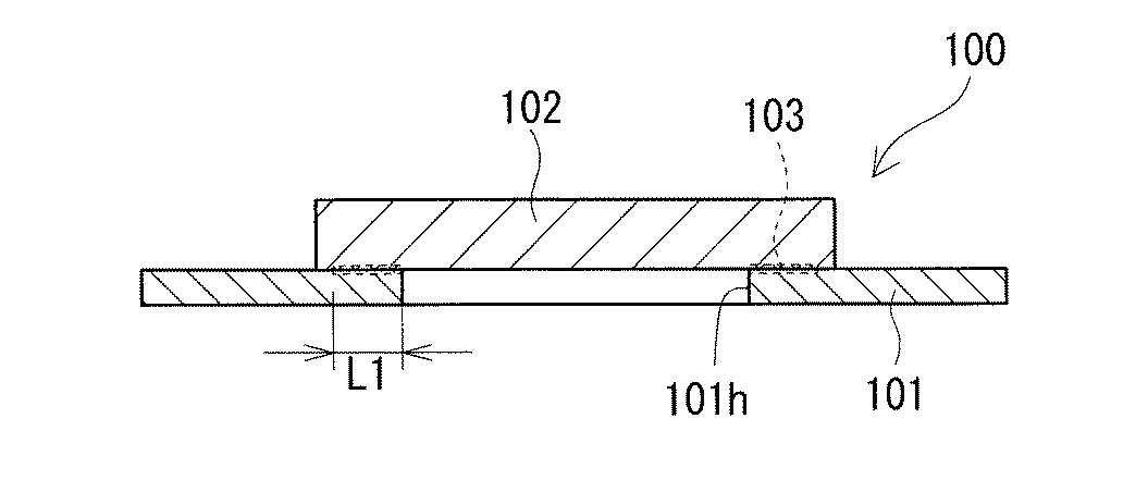
表1に示すように、試料No.1、No.2の第一試験片100は、エアの圧力が200kPa〜500kPaのいずれであっても水中に気泡が発生しなかった。試料No.3の第一試験片100は、エアの圧力が200kPaと300kPaでは水中に気泡が発生しなかった。試料No.101〜No.103の第一試験片100は、エアの圧力が200kPa〜500kPaのいずれであっても水中に気泡が発生した。これらの結果から、試料No.1〜No.3の防水性能が高いこと、特に、試料No.1、No.2の防水性能が高いことがわかる。即ち、溶着部を備えることで、防水性能に優れることがわかる。
As shown in Table 1, the sample No. 1, No. In the
表2に示すように、試料No.1〜No.3の第二試験片200の最大引張応力は、2.5MPa以上であった。また、試料No.2の第二試験片200の最大引張応力は、4.5MPa以上であり、試料No.3の1.8倍程度であった。試料No.1の第二試験片200の最大引張応力は、6.5MPa以上であり、試料No.3の2.5倍程度であった。これらの結果から、試料No.1〜No.3の接着性能が高いこと、特に、試料No.1,No.2の接着性能が高いことがわかる。即ち、溶着部を備えることで、接着性能に優れることがわかる。
As shown in Table 2, the sample No. 1-No. The maximum tensile stress of the
本発明は、これらの例示に限定されるものではなく、特許請求の範囲によって示され、特許請求の範囲と均等の意味および範囲内でのすべての変更が含まれることが意図される。 The present invention is not limited to these examples, and is indicated by the scope of claims, and is intended to include all modifications within the meaning and scope equivalent to the scope of claims.
1 コネクタ装置
2 回路基板
20 導体路
21 導体パターン
22 半田
3 コネクタ
31 ハウジング
32 端子
33 取付部
34 固定部材
4 モールド樹脂部
40 痕跡部
5 溶着部
100 第一試験片
101 円環部材
101h 貫通孔
102 円板部材
103 溶着部
200 第二試験片
201 第一矩形板材
202 第二矩形板材
203 溶着部
1
Claims (9)
コネクタと、
モールド樹脂部とを備え、
前記回路基板は、導体路を有し、
前記コネクタは、
樹脂を含むハウジングと、
前記ハウジングから突出して前記導体路に接続される端子とを有し、
前記モールド樹脂部は、前記導体路と、前記ハウジングから突出された端子と、前記ハウジングの一部とをまとめて覆い、
前記ハウジングと前記モールド樹脂部とは、互いの構成材料が溶着されてなる溶着部を有する、
コネクタ装置。 With the circuit board
With the connector
Equipped with a mold resin part,
The circuit board has a conductor path and has a conductor path.
The connector is
With a housing containing resin
It has a terminal that protrudes from the housing and is connected to the conductor path.
The mold resin portion collectively covers the conductor path, the terminal protruding from the housing, and a part of the housing.
The housing and the mold resin portion have a welded portion formed by welding each other's constituent materials.
Connector device.
前記モールド樹脂部の透過率が40%以上である請求項1に記載のコネクタ装置。 The ratio (b1 / a1) x 100 of the amount of light a1 of the laser having a wavelength of 940 nm and the amount of light b1 transmitted by the laser through the test piece having a thickness of 2 mm made of the constituent material of the mold resin portion is determined by the mold resin portion. When it comes to transmittance
The connector device according to claim 1, wherein the transmittance of the molded resin portion is 40% or more.
前記ハウジングの透過率が10%以下である請求項1又は請求項2に記載のコネクタ装置。 The transmittance (b2 / a2) × 100 of the light amount a2 of the laser having a wavelength of 940 nm and the light amount b2 transmitted by the laser through the test piece having a thickness of 2 mm made of the constituent material of the housing is defined as the transmittance of the housing. When
The connector device according to claim 1 or 2, wherein the transmittance of the housing is 10% or less.
Priority Applications (3)
| Application Number | Priority Date | Filing Date | Title |
|---|---|---|---|
| JP2019105729A JP2020202010A (en) | 2019-06-05 | 2019-06-05 | Connector device |
| CN202010418856.6A CN112054321A (en) | 2019-06-05 | 2020-05-18 | connector device |
| US16/882,578 US11251553B2 (en) | 2019-06-05 | 2020-05-25 | Connector device that includes welded portion |
Applications Claiming Priority (1)
| Application Number | Priority Date | Filing Date | Title |
|---|---|---|---|
| JP2019105729A JP2020202010A (en) | 2019-06-05 | 2019-06-05 | Connector device |
Publications (1)
| Publication Number | Publication Date |
|---|---|
| JP2020202010A true JP2020202010A (en) | 2020-12-17 |
Family
ID=73609447
Family Applications (1)
| Application Number | Title | Priority Date | Filing Date |
|---|---|---|---|
| JP2019105729A Pending JP2020202010A (en) | 2019-06-05 | 2019-06-05 | Connector device |
Country Status (3)
| Country | Link |
|---|---|
| US (1) | US11251553B2 (en) |
| JP (1) | JP2020202010A (en) |
| CN (1) | CN112054321A (en) |
Families Citing this family (2)
| Publication number | Priority date | Publication date | Assignee | Title |
|---|---|---|---|---|
| JP6930500B2 (en) * | 2018-06-22 | 2021-09-01 | 株式会社オートネットワーク技術研究所 | Circuit board equipment |
| JP7319594B2 (en) * | 2020-03-06 | 2023-08-02 | 株式会社オートネットワーク技術研究所 | connector device |
Citations (5)
| Publication number | Priority date | Publication date | Assignee | Title |
|---|---|---|---|---|
| JP2006185885A (en) * | 2004-12-01 | 2006-07-13 | Hitachi Ltd | Controller unit |
| JP2009143217A (en) * | 2007-11-20 | 2009-07-02 | Ube Ind Ltd | Laser light irradiation condition control method and laser welding processing method |
| JP2010040992A (en) * | 2008-08-08 | 2010-02-18 | Hitachi Ltd | Method of manufacturing electronic control device, its transfer molding equipment and electronic control device |
| JP2019003779A (en) * | 2017-06-13 | 2019-01-10 | 株式会社エクセル電子 | Waterproof connector and manufacturing method thereof, and electronic apparatus |
| WO2019039244A1 (en) * | 2017-08-25 | 2019-02-28 | 日立オートモティブシステムズ株式会社 | Resin-sealed on-board electronic control device |
Family Cites Families (31)
| Publication number | Priority date | Publication date | Assignee | Title |
|---|---|---|---|---|
| US4775333A (en) * | 1985-12-23 | 1988-10-04 | Ford Motor Company | Method of assembling an improved electrical connector |
| US5244409A (en) * | 1990-07-12 | 1993-09-14 | Woodhead Industries, Inc. | Molded connector with embedded indicators |
| US5567175A (en) * | 1995-05-01 | 1996-10-22 | Woods Industries, Inc. | Premold insert for a transparent plug |
| DE19755497C1 (en) * | 1997-12-13 | 1999-07-08 | Hella Kg Hueck & Co | Vehicle circuit board housing |
| EP1075713A1 (en) * | 1998-05-01 | 2001-02-14 | Vehicle Enhancement Systems, Inc | Modular connector |
| US6139365A (en) * | 1998-11-10 | 2000-10-31 | Hon Hai Precision Ind. Co., Ltd. | Centronic connector assembly |
| DE10013218C2 (en) * | 2000-03-17 | 2003-06-05 | Balluff Gmbh | Method for producing a position sensor and position sensor |
| CN2585308Y (en) * | 2002-10-25 | 2003-11-05 | 互亿科技股份有限公司 | An information device with both waterproof and light-guiding properties |
| JP2004157258A (en) * | 2002-11-05 | 2004-06-03 | Mitsubishi Cable Ind Ltd | Optical connector and locking method for plastic optical fiber |
| US6655975B1 (en) * | 2002-12-13 | 2003-12-02 | Delta Systems, Inc. | Sealed housing assembly |
| JP4207753B2 (en) * | 2003-10-31 | 2009-01-14 | 株式会社デンソー | Resin housing structure for electrical circuit equipment |
| JP2006328993A (en) * | 2005-05-24 | 2006-12-07 | Kokusan Denki Co Ltd | Waterproof electronic circuit unit |
| US7722362B2 (en) * | 2006-06-22 | 2010-05-25 | Watlow Electric Manufacturing Company | Sensor adaptor circuit housing incapsulating connection of an input connector with a wire |
| CN102648500B (en) * | 2009-11-25 | 2013-12-18 | 株式会社自动网络技术研究所 | Process for producing wire harness, and wire harness |
| JP5648362B2 (en) * | 2010-08-10 | 2015-01-07 | 住友電気工業株式会社 | Method for producing mold for nanoimprint, method for producing resin pattern by nanoimprint method, and mold for nanoimprint |
| JP2012231004A (en) * | 2011-04-26 | 2012-11-22 | Honda Elesys Co Ltd | Conduction terminal solder stress prevention structure |
| US9039442B2 (en) * | 2011-11-10 | 2015-05-26 | Carmen Rapisarda | Solder-less electrical assembly |
| JP5829559B2 (en) * | 2012-03-21 | 2015-12-09 | 矢崎総業株式会社 | Wire protection structure |
| JP5975209B2 (en) * | 2012-03-21 | 2016-08-23 | 矢崎総業株式会社 | Wire drawer partial structure |
| KR101393927B1 (en) * | 2012-08-16 | 2014-05-12 | 기아자동차주식회사 | Multimedia Jack For Vehicle With Lighting Apparatus |
| KR101428933B1 (en) * | 2013-07-05 | 2014-08-08 | 현대오트론 주식회사 | Electronic control apparatus for vehicle using radiation board and manufacturing method thereof |
| WO2015005557A1 (en) * | 2013-07-12 | 2015-01-15 | 주식회사 코리아하이텍 | Terminal connection device having light source module |
| US9379477B2 (en) * | 2013-12-20 | 2016-06-28 | Dai-Ichi Seiko Co., Ltd. | Seal having a packing portion extending from a flat portion with a step |
| JP6295100B2 (en) * | 2014-02-28 | 2018-03-14 | 日立オートモティブシステムズ株式会社 | Electronic control unit |
| US9293870B1 (en) * | 2015-03-10 | 2016-03-22 | Continental Automotive Systems, Inc. | Electronic control module having a cover allowing for inspection of right angle press-fit pins |
| CN104852176B (en) * | 2015-05-05 | 2024-03-29 | 连展科技(深圳)有限公司 | Socket electric connector |
| JP6524808B2 (en) | 2015-06-08 | 2019-06-05 | 株式会社デンソー | Electronic device |
| US10050371B2 (en) * | 2015-08-19 | 2018-08-14 | Pei-Lun Wang | Composite connection socket |
| TWI569529B (en) * | 2015-10-06 | 2017-02-01 | 飛宏科技股份有限公司 | Power plug device and the manufacturing method thereof |
| EP3462820B1 (en) * | 2017-09-29 | 2021-08-04 | Hosiden Corporation | Connector box and method of its assembly |
| DE102018100780A1 (en) * | 2018-01-15 | 2019-07-18 | Endress+Hauser SE+Co. KG | Protective device for a plug connection |
-
2019
- 2019-06-05 JP JP2019105729A patent/JP2020202010A/en active Pending
-
2020
- 2020-05-18 CN CN202010418856.6A patent/CN112054321A/en active Pending
- 2020-05-25 US US16/882,578 patent/US11251553B2/en active Active
Patent Citations (5)
| Publication number | Priority date | Publication date | Assignee | Title |
|---|---|---|---|---|
| JP2006185885A (en) * | 2004-12-01 | 2006-07-13 | Hitachi Ltd | Controller unit |
| JP2009143217A (en) * | 2007-11-20 | 2009-07-02 | Ube Ind Ltd | Laser light irradiation condition control method and laser welding processing method |
| JP2010040992A (en) * | 2008-08-08 | 2010-02-18 | Hitachi Ltd | Method of manufacturing electronic control device, its transfer molding equipment and electronic control device |
| JP2019003779A (en) * | 2017-06-13 | 2019-01-10 | 株式会社エクセル電子 | Waterproof connector and manufacturing method thereof, and electronic apparatus |
| WO2019039244A1 (en) * | 2017-08-25 | 2019-02-28 | 日立オートモティブシステムズ株式会社 | Resin-sealed on-board electronic control device |
Also Published As
| Publication number | Publication date |
|---|---|
| US11251553B2 (en) | 2022-02-15 |
| US20200388945A1 (en) | 2020-12-10 |
| CN112054321A (en) | 2020-12-08 |
Similar Documents
| Publication | Publication Date | Title |
|---|---|---|
| JP2020202010A (en) | Connector device | |
| JP5380749B2 (en) | Wire harness and manufacturing method thereof | |
| WO2021177426A1 (en) | Connector device | |
| JP2011028853A (en) | Molded connector | |
| CN102377069B (en) | Waterproof electrical connector and waterproof electrical connector assembly method | |
| JP7565153B2 (en) | VEHICLE RADOME AND METHOD FOR MANUFACTURING SAME | |
| US20090275227A1 (en) | Packing Protection Cap and Connector | |
| US10638595B2 (en) | Electric device with a housing with pressing elements | |
| TWM317660U (en) | Connecting structure for electric wires | |
| JP2018181522A (en) | Electrical connector | |
| JP2015026443A (en) | Connector fixing structure and manufacturing method of the same | |
| JP7319595B2 (en) | CONNECTOR DEVICE AND METHOD FOR MANUFACTURING CONNECTOR DEVICE | |
| JP2008215959A (en) | Radio equipment for water meter | |
| JP5814172B2 (en) | Method for manufacturing intraoral sensor | |
| JP6323066B2 (en) | Electronics | |
| JP5835143B2 (en) | Manufacturing method of resin case | |
| JP4110383B2 (en) | Proximity sensor | |
| JP3732657B2 (en) | Covered wire connection method and connection structure | |
| WO2006068229A1 (en) | Connector for electric fuse igniter | |
| US7172469B2 (en) | Structure of bonding plastic part insert-molded with wiring board and method of bonding the same | |
| US20230155317A1 (en) | Moisture-protected electrical connection | |
| JP2019071253A (en) | Sensor device and method for manufacturing the same | |
| JP2004103306A (en) | Discharge lamp base for automobile and discharge lamp for automobile | |
| JP7052682B2 (en) | Proximity sensor | |
| WO2025142795A1 (en) | Capacitor and method for manufacturing capacitor |
Legal Events
| Date | Code | Title | Description |
|---|---|---|---|
| A621 | Written request for application examination |
Free format text: JAPANESE INTERMEDIATE CODE: A621 Effective date: 20210928 |
|
| A977 | Report on retrieval |
Free format text: JAPANESE INTERMEDIATE CODE: A971007 Effective date: 20220627 |
|
| A131 | Notification of reasons for refusal |
Free format text: JAPANESE INTERMEDIATE CODE: A131 Effective date: 20220630 |
|
| A521 | Request for written amendment filed |
Free format text: JAPANESE INTERMEDIATE CODE: A523 Effective date: 20220824 |
|
| A131 | Notification of reasons for refusal |
Free format text: JAPANESE INTERMEDIATE CODE: A131 Effective date: 20221222 |
|
| A02 | Decision of refusal |
Free format text: JAPANESE INTERMEDIATE CODE: A02 Effective date: 20230622 |