JP2019153766A - Light emitting device and manufacturing method thereof - Google Patents
Light emitting device and manufacturing method thereof Download PDFInfo
- Publication number
- JP2019153766A JP2019153766A JP2018106395A JP2018106395A JP2019153766A JP 2019153766 A JP2019153766 A JP 2019153766A JP 2018106395 A JP2018106395 A JP 2018106395A JP 2018106395 A JP2018106395 A JP 2018106395A JP 2019153766 A JP2019153766 A JP 2019153766A
- Authority
- JP
- Japan
- Prior art keywords
- light emitting
- resin body
- emitting device
- extending
- extending portion
- Prior art date
- Legal status (The legal status is an assumption and is not a legal conclusion. Google has not performed a legal analysis and makes no representation as to the accuracy of the status listed.)
- Granted
Links
Images


Classifications
-
- H10W90/753—
-
- H10W90/756—
Landscapes
- Structures Or Materials For Encapsulating Or Coating Semiconductor Devices Or Solid State Devices (AREA)
- Encapsulation Of And Coatings For Semiconductor Or Solid State Devices (AREA)
- Led Device Packages (AREA)
Abstract
【課題】小型の発光装置およびその製造方法を提供する。【解決手段】発光装置100は、複数の発光素子5と、発光素子5が載置される2つの金属部2と、2つの金属部2を固定すると共に上面視において直交して隣り合う2つの辺を接続する4つの接続部7を形成した樹脂体1と、を有するパッケージ10と、を備え、金属部2のそれぞれは、発光素子5が1つ以上載置されるダイパッド3と、ダイパッド3から延伸した2つの延伸部4と、を備え、上面視において、樹脂体1に形成された接続部7から延伸部4の先端4aが露出し、延伸部4の先端4aが、樹脂体1の接続部7に隣接する辺の延長線よりも接続部7側に配置されている。【選択図】図1PROBLEM TO BE SOLVED: To provide a small light emitting device and a method for manufacturing the same. SOLUTION: A light emitting device 100 fixes a plurality of light emitting elements 5, two metal parts 2 on which the light emitting elements 5 are placed, and two metal parts 2 and two adjacent metal parts 2 orthogonally in a top view. A package 10 having a resin body 1 forming four connecting portions 7 connecting sides thereof is provided, and each of the metal portions 2 includes a die pad 3 on which one or more light emitting elements 5 are placed, and a die pad 3. The tip 4a of the stretched portion 4 is exposed from the connecting portion 7 formed in the resin body 1 and the tip 4a of the stretched portion 4 is the resin body 1. It is arranged on the connection portion 7 side with respect to the extension line of the side adjacent to the connection portion 7. [Selection diagram] Fig. 1
Description
本開示は、発光装置およびその製造方法に関する。 The present disclosure relates to a light emitting device and a manufacturing method thereof.
従来、リード端子と樹脂体とを含むパッケージと、パッケージの凹部に載置された発光素子と、を備える発光装置が知られている(特許文献1参照)。この発光装置は、リード端子をパッケージの四隅から側方に露出させている。パッケージから側方に露出したリード端子の長さは、隣り合う発光装置において対向するリード端子が、それぞれ、同一の電極に接続するのに十分な長さである。 2. Description of the Related Art Conventionally, a light emitting device including a package including a lead terminal and a resin body and a light emitting element placed in a recess of the package is known (see Patent Document 1). In this light emitting device, lead terminals are exposed to the side from the four corners of the package. The length of the lead terminal exposed to the side from the package is long enough for the lead terminals facing each other in adjacent light emitting devices to be connected to the same electrode.
発光装置が、パッケージから側方にリード端子を露出させた構造では、発光装置の外形サイズが大きくなってしまうという問題がある。 If the light emitting device has a structure in which the lead terminals are exposed laterally from the package, there is a problem that the outer size of the light emitting device becomes large.
そこで、本開示に係る実施形態は、小型の発光装置およびその製造方法を提供する。 Therefore, an embodiment according to the present disclosure provides a small light emitting device and a manufacturing method thereof.
本開示の実施形態に係る発光装置は、複数の発光素子と、前記発光素子が載置される2つの金属部と、前記2つの金属部を固定すると共に上面視において直交して隣り合う2つの辺を接続する4つの接続部を形成した樹脂体と、を有するパッケージと、を備え、前記金属部のそれぞれは、前記発光素子が1つ以上載置されるダイパッドと、前記ダイパッドから延伸した2つの延伸部と、を備え、上面視において、前記樹脂体に形成された前記接続部から前記延伸部の先端が露出し、前記延伸部の先端が、前記樹脂体の前記接続部に隣接する辺の延長線よりも前記接続部側に配置されている。 A light-emitting device according to an embodiment of the present disclosure includes a plurality of light-emitting elements, two metal parts on which the light-emitting elements are mounted, two two metal parts fixed to each other and orthogonally adjacent in a top view. Each of the metal parts, a die pad on which one or more of the light-emitting elements are mounted, and 2 extending from the die pad. Two extending portions, and the top end of the extending portion is exposed from the connecting portion formed on the resin body in a top view, and the leading end of the extending portion is adjacent to the connecting portion of the resin body. It is arrange | positioned rather than the extended line of the said connection part side.
本開示の実施形態に係る発光装置の製造方法は、金属フレームと、2つのダイパッドと、各ダイパッドから前記金属フレームの側に延伸した2つの延伸部と、を備えるリードフレームを準備する工程と、前記2つのダイパッドを固定すると共に上面視において直交して隣り合う2つの辺を接続する4つの接続部を形成した樹脂体を成形する工程と、前記ダイパッドに発光素子を載置する工程と、前記発光素子を封止する工程と、前記リードフレームを切断する工程と、を有し、前記樹脂体を成形する工程において、前記樹脂体に形成された前記接続部から前記延伸部の先端が露出するように前記樹脂体を成形し、前記リードフレームを切断する工程は、前記樹脂体を切断することなく、上面視において、前記延伸部の先端が、前記樹脂体の前記接続部に隣接する辺の延長線よりも前記接続部側に配置されるように前記延伸部を前記金属フレームから切り離す。 A method of manufacturing a light emitting device according to an embodiment of the present disclosure includes a step of preparing a lead frame including a metal frame, two die pads, and two extending portions extending from the die pads to the metal frame. Fixing the two die pads and forming a resin body in which four connection portions that connect two adjacent sides orthogonal to each other when viewed from above are formed; placing a light emitting element on the die pad; and A step of sealing the light emitting element and a step of cutting the lead frame, and in the step of molding the resin body, a tip of the extending portion is exposed from the connection portion formed in the resin body. The step of forming the resin body and cutting the lead frame in the above manner is such that the front end of the extending portion is in front of the resin body in a top view without cutting the resin body. Said extending portion so as to be disposed on the connecting portion side from the extension of the side adjacent to the connecting portion disconnected from the metal frame.
本開示に係る実施形態によれば、小型の発光装置を提供することができる。 According to the embodiment according to the present disclosure, a small light emitting device can be provided.
以下、実施形態に係る発光装置、及びその製造方法について説明する。なお、以下の説明において参照する図面は、実施形態を概略的に示したものであるため、各部材のスケールや間隔、位置関係などが誇張、あるいは、部材の一部の図示が省略されている場合がある。また、平面図とその断面図において、各部材のスケールや間隔が一致しない場合もある。また、以下の説明では、同一の名称及び符号については原則として同一又は同質の部材を示しており、詳細な説明を適宜省略することとする。また、本明細書において、「上」、「下」などは構成要素間の相対的な位置を示すものであって、絶対的な位置を示すことを意図したものではない。 Hereinafter, the light emitting device according to the embodiment and the manufacturing method thereof will be described. The drawings referred to in the following description schematically show the embodiment, and therefore, the scale, interval, positional relationship, etc. of each member are exaggerated, or some of the members are not shown. There is a case. In addition, the scale and interval of each member may not match in the plan view and the cross-sectional view thereof. Moreover, in the following description, the same name and the code | symbol are showing the same or the same member in principle, and suppose that detailed description is abbreviate | omitted suitably. Further, in this specification, “upper”, “lower” and the like indicate relative positions between components, and are not intended to indicate absolute positions.
<第1実施形態>
[発光装置の構成]
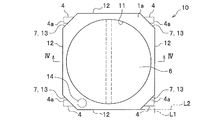
図面を用いて説明する。図1は、第1実施形態に係る発光装置の概略を示す図であり、発光装置の上面図である。図2は、第1実施形態に係る発光装置のパッケージの上面図である。図3は、第1実施形態に係る発光装置のパッケージの下面図である。図4は、第1実施形態に係る発光装置のパッケージの断面図であり、図2のIV−IV断面矢視図である。
<First Embodiment>
[Configuration of light emitting device]
This will be described with reference to the drawings. FIG. 1 is a diagram schematically illustrating the light emitting device according to the first embodiment, and is a top view of the light emitting device. FIG. 2 is a top view of the package of the light emitting device according to the first embodiment. FIG. 3 is a bottom view of the package of the light emitting device according to the first embodiment. 4 is a cross-sectional view of the package of the light emitting device according to the first embodiment, and is a cross-sectional view taken along the line IV-IV in FIG.
発光装置100は、パッケージ10と、このパッケージ10に設けた複数の発光素子5と、を備えている。パッケージ10は、樹脂体1と、2つの金属部2と、を有しており、発光素子5を金属部2に実装して収容する凹部11が形成されている。樹脂体1は、2つの金属部2を固定するものである。樹脂体1は、上面視において樹脂体1を内包する最小の矩形を構成する4辺と、これら4辺間に位置する4つの接続部7を備える。つまり、樹脂体1には、上面視において直交して隣り合う2つの辺を接続する4つの接続部7が形成されている。金属部2は、発光素子5が1つ以上載置されるダイパッド3と、ダイパッド3から延伸した2つの延伸部4と、を備えている。上面視において、樹脂体1に形成された接続部7から延伸部4の先端4aが露出している。上面視において、延伸部4の先端4aは、樹脂体1の接続部7に隣接する辺の延長線L1、L2よりも接続部7側に配置されている。
The
上面視で、発光装置100は、リードとしての延伸部4が、樹脂体1を矩形枠に当てはめた場合に矩形枠の中に収まっているので、発光装置の外形サイズを小型化することができる。
また、複数の発光装置100をマトリクス状に配置して使用する場合、発光装置100の樹脂体1の各長辺を、他の発光装置100の樹脂体1の各長辺と密接させた状態で配置することができる。つまり、上面視において、複数の発光装置100を隙間を空けることなく並設することが可能となる。
また、従来のパッケージから側方にリード端子を露出させた発光装置では、リードを切断する個片化の精度によって、発光装置の外形寸法が変わってしまう。これに対して、本実施形態の発光装置100は、樹脂の成形精度によって、発光装置の外形寸法を精度よく決定することができ、信頼性も高めることができる。
When viewed from above, the
When a plurality of
Further, in the light emitting device in which the lead terminals are exposed to the side from the conventional package, the outer dimensions of the light emitting device are changed depending on the accuracy of singulation of the leads. On the other hand, the light-emitting
<樹脂体1の構成>
上面視において、樹脂体1の外縁形状は八角形である。この八角形は、4つの長辺12と、4つの接続部7としての傾斜短辺13と、を有している。傾斜短辺13は、長辺12よりも短く長辺12に対して傾斜している。傾斜短辺13の傾斜角は、図示した45度に限定されるものではない。樹脂体1に形成された接続部7は、上面視において、傾斜短辺13に相当する。接続部7としての傾斜短辺13から延伸部4の先端4aが露出している。
<Configuration of
In the top view, the outer edge shape of the
一般に、発光装置を搬送するためにエンボスキャリアテープが用いられている。通常のエンボスキャリアテープは、上面視した形状が正方形または長方形で断面視において凹状の収容部を備えており、この収容部に発光装置を収容する。上面視した形状が正方形または長方形の発光装置であれば、凹状の収容部の側面と発光装置の側面との接触面積は、比較的大きい。一方、八角形の発光装置の場合、凹状の収容部の側面と発光装置の側面との接触面積が、小さくなるため、エンボスキャリアテープを用いて搬送すると、搬送により生ずる振動等のために、発光装置が回転する虞がある。しかしながら、発光装置100は、上面視で樹脂体1が八角形であったとしても、傾斜短辺13から延伸部4の先端4aが露出して矩形と同等な構造となっているので、搬送中の発光装置の回転を防止することができる。
In general, an embossed carrier tape is used to transport the light emitting device. A typical embossed carrier tape has a square or rectangular shape in a top view and has a concave accommodating portion in a sectional view, and a light emitting device is accommodated in the accommodating portion. If the top view shape is a square or rectangular light emitting device, the contact area between the side surface of the concave housing portion and the side surface of the light emitting device is relatively large. On the other hand, in the case of an octagonal light-emitting device, the contact area between the side surface of the concave housing portion and the side surface of the light-emitting device is small, so when transported using an embossed carrier tape, light emission occurs due to vibrations etc. caused by transport. The device may rotate. However, even if the
上面視において、複数の発光素子5を取り囲む樹脂体1の内縁形状(つまりパッケージ10の凹部11の内側面形状)は、円形であることが好ましい。このようにすることで、発光装置100の発光面形状を円形にすることができる。また、樹脂体1における環状の壁部15の内側面は、樹脂体1の下面1bから上面1aに向かって広がるように傾斜していることが好ましい。
また、上面視において、樹脂体1の内縁形状が円形の場合、樹脂体1の外縁形状が八角形であれば、樹脂体の外縁形状が正方形または長方形であるときに比べて、環状の壁部15の厚みをより均一にすることができる。壁部15の厚みを均一に近づけることで、熱による膨張や収縮を均一にすることができ、熱応力を均等に分散することができる。
When viewed from above, the inner edge shape of the
Further, when the inner edge shape of the
樹脂体1の側面1cは、図4に示すように、樹脂体1の上面1aに連続するように形成されると共に、樹脂体1の下面1bにも連続するように形成されている。なお、凹部11の底面において、中央に露出する樹脂体1の一部は、2つのダイパッド3を正負一対の電極として隔てるための絶縁部となっている。
As shown in FIG. 4, the
樹脂体1は、2つのダイパッド3の一方の側に、極性を示すマーク14が形成されている。マーク14は、カソードマークまたはアノードマークである。マーク14は、樹脂体1の上面1aに形成されることが好ましい。
The
樹脂体1は、2つの金属部2を固定すると共に壁部15を構成している。樹脂体1は、壁部15から、一対のダイパッド3間に連続的に形成されている。樹脂体1を構成する樹脂としては、例えば熱可塑性樹脂や熱硬化性樹脂を挙げることができる。
熱可塑性樹脂の場合、例えば、ポリフタルアミド樹脂、液晶ポリマー、ポリブチレンテレフタレート(PBT)、不飽和ポリエステル等を用いることができる。
熱硬化性樹脂の場合、例えば、エポキシ樹脂、変性エポキシ樹脂、シリコーン樹脂、変性シリコーン樹脂、ウレタン樹脂、アクリレート樹脂等を用いることができる。
The
In the case of a thermoplastic resin, for example, polyphthalamide resin, liquid crystal polymer, polybutylene terephthalate (PBT), unsaturated polyester, or the like can be used.
In the case of a thermosetting resin, for example, an epoxy resin, a modified epoxy resin, a silicone resin, a modified silicone resin, a urethane resin, an acrylate resin, or the like can be used.
壁部15の内側面において光を効率よく反射するために、樹脂体1を構成する樹脂に光反射部材が含有されていても構わない。例えば酸化チタン、酸化亜鉛、酸化ジルコニウム、酸化アルミニウム、酸化ケイ素、ガラスフィラー、シリカ、酸化マグネシウム、酸化アンチモン、水酸化アルミニウム、硫酸バリウム、炭酸マグネシウム、炭酸バリウムは、水分等に対して比較的安定でかつ高屈折率であり、また熱伝導性にも優れるため好ましい。
In order to reflect light efficiently on the inner surface of the
<金属部2の構成>
金属部2の材質は、例えば銅、鉄、アルミニウム、又はそれらを含む合金が好ましい。金属部2のうち、凹部11の底面に露出した表面にはメッキが施されている。これにより、発光素子5からの光の反射率を高めることができる。メッキとしては、例えば、金、銀、ニッケル、パラジウム、アルミニウムなどを用いることができ、単層メッキまたは、積層メッキとすることができる。また、金属部2のうちパッケージ10の下面から露出した表面にもメッキを施すことが好ましい。これにより、半田等の導電性部材との接合強度を上げることができる。
<Configuration of
The material of the
2つのダイパッド3は、上面視で対称に形成されることが好ましい。このようにすることで、発光装置裏面に対称な電極形状が形成され、発光装置100を外部の実装基板に例えば半田で実装(2次実装)する際に、非対称の場合と比べて、位置合わせを精度よく行うことができる。ここで対称とは、一部を変形させた略対称な形状も含む。このように一部を変形させることで、位置合わせを精度よく行う効果は維持したまま、2つのダイパッドの判別が可能となる。
The two die
図3に示すように、パッケージ10の下面には、2つのダイパッド3の裏面が露出している。2つのダイパッド3が対称に形成されていると、放熱性が左右均等になり易く放熱バランスがよい。また、発光装置100は、放熱バランスが良好なので、多数の発光素子5を載置して出力を高めることができる。
As shown in FIG. 3, the back surfaces of the two die
ダイパッド3のそれぞれには、同数の発光素子5が載置されることが好ましい。ここでは、ダイパッド3のそれぞれに、4個の発光素子5が載置されており、高出力の発光装置とすることができる。なお、発光素子5の個数は、これに限定されない。また、ダイパッド3に載置された発光素子5の配置も左右対称であることが好ましい。このようにすることで、例えば、屋外の照明装置を製造する場合に、発光装置100と組み合わせて用いるレンズの設計を、非対称の場合と比べて容易化することができる。
It is preferable that the same number of
ダイパッド3は、厚みが一様な板状でもよいが、図4に示すように、側方に突出する凸部3aを設けてもよい。凸部3aは、ダイパッド3の周縁に連続してまたは断続して設けられている。凸部3aは、ダイパッド3の周縁を中央付近の厚みより薄くすることで形成
されている。この凸部3aにより、ダイパッド3と樹脂体1との密着性を向上させることができる。
The
ダイパッド3は、凹部11の底面の一部を構成している。2つのダイパッド3は、正負一対となるように離間させて配置されている。一対のダイパッド3は、アノード電極、カソード電極にそれぞれ相当し、それぞれ導電性が異なることを意味する。ダイパッド3は、略矩形に形成された樹脂体の一側の角部分の2箇所にある接続部から露出し延伸する延伸部4が形成されている。
The
延伸部4は、上面視において、例えば、樹脂体1の長辺12に平行な端面を有している。本実施形態では、延伸部4は、ダイパッド3から、樹脂体1の長辺12に沿って外側に延伸して形成されている。延伸部4は、2つのダイパッド3が並んでいる方向に延伸している。また、延伸部4が延伸している方向と直交する方向も、樹脂体1の長辺12に沿っている。図2に示すように、延伸部4の先端4aは、樹脂体1の長辺12の延長線L1と、他の長辺の延長線L2とで囲んだ領域内となる樹脂体1の側に配置されている。
The extending
延伸部4は、上面視において、発光装置100の角部に配置されているので、樹脂体1の角部の強度を向上させることができる。また、発光装置100は、上面視において、樹脂体1から延伸部4が露出している。そのため、発光装置100を外部の実装基板に例えば半田で実装(2次実装)する際に、延伸部4において、半田のフィレットの状態を観察することができる。
Since the extending | stretching
<発光素子5の構成>
発光素子5は、パッケージ10の凹部11の底面においてダイパッド3のそれぞれに配置される。発光素子5のp電極は、ワイヤ9を介してカソード側のダイパッド3または他の発光素子5のn電極と電気的に接続している。発光素子5のn電極は、ワイヤ9を介してアノード側のダイパッド3または他の発光素子5のp電極と電気的に接続している。
<Configuration of Light-Emitting
The
ここで用いられる発光素子5は形状や大きさ等が特に限定されない。発光素子5の発光色としては、用途に応じて任意の波長のものを選択することができる。例えば、青色(波長430〜490nmの光)の発光素子としては、GaN系やInGaN系を用いることができる。InGaN系としては、InXAlYGa1-X-YN(0≦X≦1、0≦Y≦1、X+Y<1)等を用いることができる。なお、発光素子5は、同一面側に正負(p,n)電極を有するものを使用することができる他、正負電極を互いに反対の面に有する対向電極構造のものも使用することができる。
The
<その他の構成>
発光装置100は、さらに、封止部材6と、保護素子8と、ワイヤ9と、を備えている。
封止部材6は、パッケージ10の凹部11内に実装された発光素子5等を覆うものである。封止部材6は、発光素子5等を、外力、埃、水分等から保護すると共に、発光素子5等の耐熱性、耐候性、耐光性を良好なものとするために設けられている。
封止部材6を構成する樹脂としては、熱硬化性樹脂、例えば、シリコーン樹脂、エポキシ樹脂、ユリア樹脂等の透明な材料を挙げることができる。このような材料に加えて、所定の機能を持たせるために、蛍光体や光反射率が高い物質等のフィラーを含有させることもできる。
<Other configurations>
The
The sealing
As resin which comprises the sealing
封止部材6を構成する樹脂は、例えば蛍光体を混合することで、発光装置100の色調調整を容易にすることができる。封止部材6を構成する樹脂に含有させるフィラーとしては、例えば、SiO2、TiO2、Al2O3、ZrO2、MgO等の光反射率が高い物
質を好適に用いることができる。また、所望外の波長をカットする目的で、例えば、有機や無機の着色染料や着色顔料を用いることができる。
The resin constituting the sealing
保護素子8としては、例えばツェナーダイオードを用いることができる。ツェナーダイオードは、発光素子5から離してダイパッド3に載置することができる。具体的には、ツェナーダイオードは、ダイパッド3において、2つのダイパッド3を絶縁する中央部の近傍で、凹部11の内側面の近傍に載置されることが好ましい。
For example, a Zener diode can be used as the
ワイヤ9は、発光素子5同士を電気的に接続したり、発光素子5や保護素子等の電子部品とダイパッド3とを電気的に接続したりするための導電性の配線である。ワイヤ9の材質としては、Au(金)、Ag(銀)、Cu(銅)、Pt(白金)、Al(アルミニウム)等の金属、及び、それらの合金を好適に用いることができる。なお、ワイヤ9の太さは特に限定されず、目的及び用途に応じて適宜選択することができる。
The
[発光装置の製造方法]
図5は、第1実施形態に係る発光装置の製造工程の概略を示す図であり、リードフレームの上面図である。図6は、リードフレームの上面図であって、図5の部分拡大図である。図7は、リードフレームの下面図であって、図5の部分拡大図である。図8は、リードフレームの断面図であって、図5のVIII−VIII断面矢視図である。図9は、第1実施形態に係る発光装置の製造工程の概略を示す図であり、樹脂体を形成した後のリードフレームの上面図である。図10は、第1実施形態に係る発光装置の製造工程の概略を示す図であり、発光素子を封止樹脂で封止した後のリードフレームの部分拡大図である。図11は、第1実施形態に係る発光装置の製造工程の概略を示す図であり、切断予定線を付したリードフレームの部分拡大図である。図6および図7は、図5にAで示す領域の部分拡大図である。図10および図11は、図9にBで示す領域の部分拡大図である。
[Method for Manufacturing Light Emitting Device]
FIG. 5 is a diagram schematically showing the manufacturing process of the light emitting device according to the first embodiment, and is a top view of the lead frame. FIG. 6 is a top view of the lead frame, and is a partially enlarged view of FIG. FIG. 7 is a bottom view of the lead frame, and is a partially enlarged view of FIG. FIG. 8 is a cross-sectional view of the lead frame, and is a cross-sectional view taken along the line VIII-VIII in FIG. FIG. 9 is a diagram schematically illustrating the manufacturing process of the light emitting device according to the first embodiment, and is a top view of the lead frame after the resin body is formed. FIG. 10 is a diagram illustrating an outline of the manufacturing process of the light emitting device according to the first embodiment, and is a partially enlarged view of the lead frame after the light emitting element is sealed with a sealing resin. FIG. 11 is a diagram showing an outline of the manufacturing process of the light emitting device according to the first embodiment, and is a partially enlarged view of the lead frame with a cut line. 6 and 7 are partially enlarged views of a region indicated by A in FIG. 10 and 11 are partially enlarged views of a region indicated by B in FIG.
第1実施形態に係る発光装置の製造方法は、準備工程と、成形工程と、素子載置工程と、封止工程と、切断工程と、を有する。
準備工程では、リードフレーム20を準備する。リードフレーム20は、平板状の金属板に打ち抜き加工やエッチング加工等を行ったものである。
図5〜図8に示すリードフレーム20は、金属フレーム21と、吊りリード22と、2つのダイパッド23と、各ダイパッド23から金属フレーム21の側に延伸した2つの延伸部24と、を備える。ここで、リードフレーム20におけるダイパッド23とは、成形後のダイパッド3に相当する部分を意味し、個片化する前の状態をいう。2つのダイパッド23は、上面視で対称に形成されている。また、リードフレーム20における延伸部24とは、成形後の延伸部4に相当する部分を意味し、個片化する前の状態をいう。
The manufacturing method of the light-emitting device according to the first embodiment includes a preparation process, a molding process, an element mounting process, a sealing process, and a cutting process.
In the preparation step, the
The
リードフレーム20は、個片化後に発光装置となる発光装置部がマトリクス状に配置されており、複数のスリット31が形成されている。ここでは、スリット31は、列方向(縦)に並ぶ3個の発光装置部を行ごと(横)に分離するような形状である。スリット31は、列方向(縦)に隣接する複数の発光装置部を離間させるための貫通孔として機能する。このスリット31は、各発光装置部において、個片化後のリードを正負一対の電極とする絶縁部を設けるための貫通孔としての役割も果たしている。
The
また、リードフレーム20には、行方向に複数の貫通孔32が形成されている。貫通孔32は、発光装置部を区分するために設けられ、ここでは、発光装置部の左右それぞれに形成されている。スリット31や貫通孔32は、樹脂で完全に埋められるのではなく、樹脂は、スリット31の一部分や貫通孔32の一部分に充填される。また、金属フレーム21において、スリット31や貫通孔32の開口周縁部で樹脂を充填される部分には、個片化後に、図4の凸部3aとなる凸部を形成してもよい。
さらに、リードフレーム20の金属フレーム21の適所には、樹脂が全く充填されない貫通孔33〜35が形成されている。貫通孔33〜35は、例えば位置合わせや軽量化のために形成されており、目的に適した形状で形成されている。
The
Furthermore, through
このような貫通孔や凸部は、エッチング加工やプレス加工等によって形成することができる。例えば、リードフレーム厚みの半分程度が加工される条件で、上面および下面側からそれぞれエッチング加工することで、貫通孔や凸部を形成することができる。このとき、貫通孔は、上面および下面の両方から加工することで形成でき、凸部は、いずれか一方の面のみから加工することで形成できる。このような加工は、上面と底面とで異なるマスクパターンを用いることで行うことができる。また、エッチング加工による加工面は曲面となることから、エッチング加工によって凸部を形成することで、曲面で構成された凸部を容易に得ることができるが、エッチング加工に限定されるものではなく、目的及び用途に応じて適宜選択することができる。 Such a through-hole and a convex part can be formed by etching or pressing. For example, through holes and protrusions can be formed by etching from the upper surface and the lower surface under conditions where about half the lead frame thickness is processed. At this time, the through hole can be formed by processing from both the upper surface and the lower surface, and the convex portion can be formed by processing from only one of the surfaces. Such processing can be performed by using different mask patterns for the top and bottom surfaces. In addition, since the processed surface by the etching process is a curved surface, by forming the convex part by the etching process, the convex part constituted by the curved surface can be easily obtained, but is not limited to the etching process. Depending on the purpose and application, it can be appropriately selected.
成形工程では、図9に示すように、2つのダイパッド23を固定する樹脂体1を成形する。樹脂体1は、例えば、リードフレーム20を上金型と下金型とで挟み込み、樹脂をトランスファ・モールドして形成する。
成形工程では、上面視において、樹脂体1の外縁形状が例えば八角形になるように、また、樹脂体1の内縁形状が例えば円形になるような金型を用いて成形する。
樹脂体1は、上面視において直交して隣り合う2つの辺を接続する4つの接続部7が形成される。また、成形工程では、樹脂体1に形成された接続部7から延伸部24の先端4aが露出するように樹脂体1を成形する。
In the molding step, as shown in FIG. 9, the
In the molding step, the
The
なお、金属部2のメッキ処理は、樹脂体1の形成前または形成後に行うことができる。樹脂体1の形成前にリードフレームにメッキ処理を施す場合、製造方法を簡略化することができ好ましい。樹脂体1の形成後に行った場合は、リードフレーム20の表面状態は、メッキ処理前の方が粗面であるため、メッキ処理前に樹脂体1を形成することで、リードフレーム20と樹脂体1との密着性を向上することができる。
The plating treatment of the
素子載置工程では、各ダイパッド23に発光素子5を載置する。各ダイパッド23には複数の発光素子5を載置することが好ましい。本実施形態では、ダイパッド23のそれぞれに、同数の発光素子5を載置する。これにより、放熱バランスが良好となる。
発光素子5と、ダイパッド23と、を接合する接合部材は、例えばダイパッド23の上面に塗布法等で形成される。なお、ダイパッド23の所定位置に保護素子8を載置してもよい。そして、発光素子5は、ワイヤ9によって、隣接する発光素子5と電気的に接続される。また、発光素子5等の所定の電子部品は、ワイヤ9によって、ダイパッド3と電気的に接続される。
In the element placing step, the
A joining member that joins the
封止工程では、発光素子5を封止する。例えば樹脂塗布装置が、複数の発光素子5の上から、封止部材6を構成する樹脂を塗布する。塗布された樹脂は、その後、硬化される。なお、この樹脂としては、例えば熱硬化性樹脂を用いることができる。また、樹脂には、蛍光体、無機フィラー、有機フィラーの少なくとも、1つを含有させることができる。樹脂の充填量を必要最小限にする場合には、封止部材6の表面を平坦な形状とする。ここでいう平坦な形状とは、樹脂のひけによる凹状も含む。なお、封止部材6にレンズ機能を持たせる場合には、表面を盛り上がらせて凸レンズ形状としてもよい。
In the sealing step, the
切断工程では、樹脂体1を切断することなく、リードフレーム20のみを切断する。
切断工程は、上面視において、延伸部24の先端4aが、樹脂体1の接続部7に隣接する辺の延長線L1、L2で囲んだ領域よりも接続部7側に配置されるように延伸部24を金属フレーム21から切り離す。切断は、延伸部24に対して切断刃が直角に当たるよう
にして切断を行うことが好ましい。切断刃が直角に近い角度で当たることで、切断時の位置ずれを生じにくくすることができる。また、斜めではなく垂直方向に切断することで、切断面の幅を小さくすることができ、切断の精度を上げることができる。ここで、樹脂体1は八角形であるが、切断方向は、樹脂体1の傾斜短辺13と平行の関係にはない。切断予定線は、図11において、延伸部24と吊りリード22との境界として示されている。この切断予定線は、樹脂体1の長辺と平行の関係にある。切断予定線に沿って切断することにより、図1に示す発光装置100を得ることができる。
In the cutting step, only the
In the cutting process, the
リードフレーム20における発光装置部には、4隅に延伸部24がそれぞれ配置されている。切断工程では、これら4か所の延伸部24と吊りリード22との境界をすべて同じ方向に切断する。これにより、延伸部24における切断面はただ1つとなる。したがって、延伸部24を2つの方向から切断して金属フレームから切り離す場合よりも延伸部24に掛かる応力を低減することができる。
The light emitting device portion in the
また、リードフレーム20は、発光装置部の4隅に延伸部24を有することから、発光装置部の左右にそれぞれ延伸部を有する形態に比べて、成形後の個片化時に、成形樹脂が割れを引き起こすような応力を、分散できる効果を奏する。つまり、切断工程において、左右のリードの端を切断して外枠のフレームから切り離す形態に比べて、四隅のリードの端を切断する方が、切断箇所ごとの応力が緩和され、成形樹脂の割れを防止することができる。
In addition, since the
また、図9に示すように、樹脂体1の形成後にも、スリット31によって複数の発光装置部を予め行ごとに分離しているため、リードフレーム20を列方向に切断するのみで個片化でき、工程数を低減できる。
Further, as shown in FIG. 9, even after the formation of the
<第1実施形態の変形例>
図12は、第1実施形態の変形例に係る発光装置の概略を示す図であり、発光装置の上面図である。発光装置100Aは、上面視において、樹脂体1の外縁形状が第1実施形態に係る発光装置100と相違している。以下では、第1実施形態に係る発光装置100と同じ構成には同じ符号を付して説明を省略する。
<Modification of First Embodiment>
FIG. 12 is a diagram schematically showing a light emitting device according to a modification of the first embodiment, and is a top view of the light emitting device. The
上面視において、樹脂体1の外縁形状は、4つの互いに対向する長辺12と、4つの接続部7としての円弧と、を有している。接続部7Aとしての円弧は、直交する2つの長辺12に連続している。接続部7Aとしての円弧は、4つの長辺12の両端を頂点として形成される八角形の内部を通過するように形成されている。接続部7Aとしての円弧から延伸部4の先端4aが露出している。この発光装置100Aも、上面視で、リードとしての延伸部4が、樹脂体1の長辺12の延長線L1、L2で囲まれる領域内に収まっているので、発光装置の外形サイズを小型化することができる。
When viewed from above, the outer edge shape of the
第1実施形態の変形例に係る発光装置の製造方法は、第1実施形態に係る発光装置の製造方法と同様である。ただし、成形工程において、金型が相違する。この場合、成形工程では、上面視において、樹脂体1の外縁形状が、八角形の4斜辺が内側に凹んだ4つの円弧を有するように、また、樹脂体1の内縁形状が例えば円形になるような金型を用いて成形する。
The manufacturing method of the light emitting device according to the modification of the first embodiment is the same as the manufacturing method of the light emitting device according to the first embodiment. However, the mold is different in the molding process. In this case, in the molding process, when viewed from above, the outer edge shape of the
<第2実施形態>
[発光装置の構成]
図13は、第2実施形態に係る発光装置の概略を示す図であり、発光装置の上面図である。発光装置100Bは、上面視において、樹脂体1の外縁形状および延伸部4Bの形状が第1実施形態に係る発光装置100と相違している。また、ここでは、ダイパッド3の
それぞれに、3個の発光素子5が載置されている。以下では、第1実施形態に係る発光装置100と同じ構成には同じ符号を付して説明を省略する。
Second Embodiment
[Configuration of light emitting device]
FIG. 13 is a diagram schematically illustrating the light emitting device according to the second embodiment, and is a top view of the light emitting device. The
発光装置100Bは、上面視において、樹脂体1の外縁形状が、4つの互いに対向する長辺12と、4つの接続部7としての折れ線部分と、を有している。折れ線部分は、直交する2つの長辺12に連続しており、折れ曲がった3本の直線で形成されている。接続部7Bとしての折れ線部分から延伸部4Bの先端4aが露出している。
In the
図13に示すように、上面視において、延伸部4Bの先端4aは、樹脂体1の接続部7Bに隣接する辺の延長線L3、L4により囲まれる領域内となる接続部7B側に配置されている。この発光装置100Bも、上面視で、リードとしての延伸部4Bが、樹脂体1を矩形にした場合の矩形枠の中に収まっているので、発光装置の外形サイズを小型化することができる。
発光装置100Bは、上面視において、延伸部4Bの先端4a側の幅W1が、延伸部4Bの基端4b側の幅W2よりも大きく形成されている。したがって、例えば発光装置100Bを実装基板へ接合するときに延伸部4Bを押え易く、作業がし易くなる。
As shown in FIG. 13, the
In the
<発光装置の製造方法>
図14は、第2実施形態に係る発光装置の製造工程の概略を示す図であり、発光素子を封止樹脂で封止した後のリードフレームの部分拡大図である。図15は、第2実施形態に係る発光装置の製造工程の概略を示す図であり、切断予定線を付したリードフレームの部分拡大図である。
<Method for manufacturing light emitting device>
FIG. 14 is a diagram schematically illustrating a manufacturing process of the light emitting device according to the second embodiment, and is a partially enlarged view of the lead frame after sealing the light emitting element with a sealing resin. FIG. 15 is a diagram showing an outline of a manufacturing process of the light emitting device according to the second embodiment, and is a partially enlarged view of the lead frame with a cutting line.
第2実施形態に係る発光装置の製造方法は、第1実施形態に係る発光装置の製造方法と同様である。ただし、準備するリードフレーム200の形状と、成形工程において使用する金型が相違する。金型については、上面視において、樹脂体1の外縁形状が、八角形の4斜辺が内側に凹んだ4つの折れ線部分を有するように、また、樹脂体1の内縁形状が例えば円形になるような形状の金型を用いる。
The manufacturing method of the light emitting device according to the second embodiment is the same as the manufacturing method of the light emitting device according to the first embodiment. However, the shape of the lead frame 200 to be prepared is different from the mold used in the molding process. As for the mold, the outer edge shape of the
図14および図15は、準備するリードフレーム200の一例の拡大図を示している。図14と図15とを対比して分かるように、切断工程では、図15において、延伸部24Bと吊りリード22との境界として示す切断予定線に沿って切断する。これにより、図13に示す発光装置100Bを得ることができる。
14 and 15 show enlarged views of an example of the lead frame 200 to be prepared. As can be seen by comparing FIG. 14 and FIG. 15, in the cutting process, cutting is performed along a planned cutting line shown as a boundary between the extending
本実施形態においても、リードフレーム20における発光装置部には、4隅に延伸部24Bがそれぞれ配置されている。切断工程では、これら4か所の延伸部24Bと吊りリード22との境界をすべて同じ方向に切断する。これにより、延伸部24Bにおける切断面はただ1つとなる。したがって、延伸部24Bを2つの方向から切断して金属フレームから切り離す場合よりも延伸部24Bに掛かる応力を低減することができる。
Also in the present embodiment, the light emitting device portion in the
また、延伸部24Bは、図1の延伸部24よりも面積が大きいので、例えば、製造時に、延伸部24Bを保持した状態で金型によって挟み易くなる。そのため、治具で延伸部24Bを保持することで成形樹脂を離型することも可能である。これにより、成形樹脂を離型するためのピンの痕跡としての凹みが形成されず、美観の優れた発光装置100Bとすることができる。加えて、マーク14を目立たせる必要がないので、マークを浅く形成することができ、樹脂体1の強度を高めることができる。
Moreover, since the extending
以上、発明を実施するための形態により具体的に説明したが、本発明の趣旨はこれらの記載に限定されるものではなく、特許請求の範囲の記載に基づいて広く解釈されなければならない。また、これらの記載に基づいて種々変更、改変などしたものも本発明の趣旨に
含まれることはいうまでもない。
The embodiments of the present invention have been specifically described above, but the gist of the present invention is not limited to these descriptions and should be widely interpreted based on the description of the scope of claims. Needless to say, various changes and modifications based on these descriptions are also included in the spirit of the present invention.
発光装置の製造方法は、リードフレームを切断する工程により得られた発光装置をエンボスキャリアテープに収納する工程をさらに有するようにしてもよい。この収納工程は、例えば、発光装置の検査工程の前後に行うことができる。または、発光装置を外部の実装基板に例えば半田で実装(2次実装)する工程の前に行うことができる。この2次実装する工程では、例えば自動挿入装置等を用いて、エンボスキャリアテープから発光装置を取り出して、例えば実装基板に2次実装する。例えば八角形の発光装置の場合、通常のエンボスキャリアテープを用いて搬送すると、搬送により生ずる振動等のために、発光装置が回転する虞がある。回転してしまった発光装置を、例えば自動挿入装置等を用いて取り出して実装基板に2次実装すると、発光装置の下面の配線パターンと実装基板の上面に設けた配線パターンとが所定の位置で接続されないこととなる。この場合、発光装置を導通させることができないこととなってしまう。
しかしながら、発光装置100、100A、100Bは、上面視において、接続部7、7A、7Bから延伸部の先端が露出しているので、エンボスキャリアテープの搬送中における発光装置の回転を防止することができる。
The manufacturing method of the light emitting device may further include a step of storing the light emitting device obtained by the step of cutting the lead frame in an embossed carrier tape. This storing step can be performed, for example, before or after the light emitting device inspection step. Alternatively, it can be performed before the step of mounting the light emitting device on an external mounting substrate with, for example, solder (secondary mounting). In this secondary mounting step, the light emitting device is taken out from the embossed carrier tape using, for example, an automatic insertion device, and then secondarily mounted on a mounting substrate, for example. For example, in the case of an octagonal light-emitting device, when a normal embossed carrier tape is used for transport, the light-emitting device may rotate due to vibrations caused by the transport. When the rotated light-emitting device is taken out using, for example, an automatic insertion device and secondarily mounted on the mounting substrate, the wiring pattern on the lower surface of the light-emitting device and the wiring pattern provided on the upper surface of the mounting substrate are placed at predetermined positions. It will not be connected. In this case, the light emitting device cannot be made conductive.
However, in the
<第3実施形態>
[発光装置の構成]
図16A〜図16Cは、第3実施形態に係る発光装置の構成を説明するための図である。なお、既に説明した発光装置の構成については同じ符号を付して説明を省略する。また、第3実施形態では、ダイパッドの所定位置に貫通孔あるいは貫通溝が形成されている構成が他の実施形態とは異なる。そのため、ここでは、主に第1実施形態に係る発光装置において、ダイパッドに形成される貫通孔あるいは貫通溝について、その形状、位置等を主として説明する。
発光装置100Cは、パッケージ10(図1参照)と、このパッケージ10に設けた複数の発光素子5(図1参照)と、を備えている。パッケージ10は、樹脂体1と、2つの金属部2と、を有しており、発光素子5を金属部2に実装して収容する凹部11(図1参照)が形成されている。樹脂体1は、2つの金属部2を固定するものである。金属部2は、発光素子5(図1参照)が1つ以上載置されるダイパッド3と、ダイパッド3から延伸した2つの延伸部4と、延伸部4の基端に隣接するダイパッド3の領域E1に板厚方向に貫通して形成された貫通孔40とを備えている。
<Third Embodiment>
[Configuration of light emitting device]
16A to 16C are diagrams for explaining the configuration of the light-emitting device according to the third embodiment. In addition, about the structure of the light-emitting device already demonstrated, the same code | symbol is attached | subjected and description is abbreviate | omitted. In the third embodiment, a configuration in which a through hole or a through groove is formed at a predetermined position of the die pad is different from the other embodiments. Therefore, here, mainly in the light emitting device according to the first embodiment, the shape, position, and the like of the through hole or the through groove formed in the die pad will be mainly described.
The
貫通孔40は、接合部材である例えばハンダHdを介して発光装置100Cが配線パターンPTに設置されるときに、発光装置100Cの位置ズレを防止する機能を有するものである。貫通孔40は、ダイパッド3の金属板面と略同一平面となるように、その孔内に樹脂が充填されている。貫通孔40の形成される位置は、延伸部4の基端に隣接するダイパッド3の領域として、予め設定された設定領域内でありここでは略矩形の領域E1内に形成されている。貫通孔40が形成される領域E1は、例えば、延伸部4の基端に隣接して延伸部4の面積の略4倍の広さとなる領域として設定されている。貫通孔40が延伸部4の基端に隣接するダイパッド3の位置に形成されることで、ハンダHdの塗布量が、発光装置100Cのダイパッド3の全体に対して偏った場合に、リフロー時に貫通孔40に充填されている樹脂がハンダHdの移動を抑制して位置ズレを防止することができる。ハンダHdは、図16A及び図16Bに示すように、例えば、一つのダイパッド3(図16C参照)に対して4カ所に塗布され、中央の2箇所のハンダh2,h3の塗布量が両端の2箇所のハンダh1,h4の塗布量よりも多くなるようになっている。ハンダHdは、ダイパッド3及び延伸部4の金属面に対しては、リフロー時に濡れ広がることで、その金属面に沿って移動する。その場合、リフロー前のハンダHdの塗布量が均等でなかった場合には、塗布量の多い側に発光装置100Cが流動性のあるハンダHdによって引っ張られてしまい予め設定された正しい位置からずれてしまうことがある。
The through-
そこで、ダイパッド3の延伸部4の基端に隣接する略矩形の領域E1に貫通孔40を形成して樹脂体1の樹脂が貫通孔40内に充填されるようにすると、ハンダHdは、樹脂の部分には濡れない。そのため、発光装置100Cは、貫通孔40の樹脂によりリフロー時のハンダHdによる延伸部4側に向かう流動の少なくとも一部又は全部が抑制されて、予め設定されている位置に接合することができるようになる。
つまり、ハンダHdは、ダイパッド3及び延伸部4の金属面に沿ってリフローにより延伸部4側に向かって、ハンダh1,h2あるいはハンダh3,h4が移動しようとする。しかし、ハンダh1,h2あるいはハンダh3,h4が、延伸部4に向かって濡れ広がろうとする経路上に貫通孔40により樹脂が金属面から露出していることで、濡れ広がろうとするハンダh1,h2あるいはハンダh3,h4の少なくとも一部の流動性を抑制することになる。ハンダHdの塗布量が、ハンダh1,h2とハンダh3,h4とにおいて略均等であれば、貫通孔40の有無にかかわらず発光装置100Cは、所定の位置にリフローにより接合される。また、ハンダHdの塗布量が、ハンダh1,h2とハンダh3,h4とにおいてある程度ばらついていても、貫通孔40により金属面から樹脂が露出していることで、ハンダHdの濡れ広がりの少なくとも一部を抑制して、発光装置100Cのリフローによる位置ズレを防止することができる。
Therefore, when the through
In other words, the solder Hd tends to move along the metal surfaces of the
そのため、貫通孔40の位置は、ダイパッド3の延伸部4の基端に隣接して、延伸部4に向かって濡れ広がるハンダHdの経路上であれば、ハンダHdの濡れ広がりを抑制することができる位置となる。貫通孔40は、延伸部4の基端に隣接して延伸部4の面積の4倍の広さの面積となるダイパッド3の領域E1内の位置に形成されていれば、前記した効果を奏することになる。
また、貫通孔40の位置は、さらに、対向する延伸部4の幅を対角線上で結んだ幅線内に全部又は少なくとも一部が重なるように形成されていることがより好ましい。貫通孔40が前記した幅線内にあることで、延伸部4の基端に対向する位置に貫通孔40が位置することとなる。そのため、ハンダHDの濡れ広がりによる発光装置100Cの位置ずれをより確実に防止することができ、かつ、貫通孔40の位置がダイパッド3の外縁からより内側になることでダイパッド3の強度を保ち易くなる。なお、発光装置100Cのリフローを行うときに仮止めする際に、貫通孔40は、配線パターンPTに塗布されるハンダHdに少なくとも一部が重ならない位置であることが、より好ましい。
Therefore, if the position of the through
Further, it is more preferable that the positions of the through
また、貫通孔40の形状は、図16A及び図16Cに示すように、円形であることや、他の形状であっても構わない。すなわち、図17Aに示すように、貫通孔41として、楕円形あるいは長丸形状であってもよい。このような円形に比べて範囲が広がることで、ハンダHdの少なくとも一部の濡れ広がりを抑制し易くなる。また、図17B及び図17Cに示すように貫通溝42あるいは貫通溝43であってもよい。貫通溝42あるいは貫通溝43にも樹脂体1の樹脂が入り込んでダイパッド3の金属面と略同一平面となるように形成されている。貫通溝42あるいは貫通溝43においても、対向する延伸部4の幅を対角線上で結んだ幅線内に少なくとも一部が重なるように形成されていることがより好ましい。貫通孔40,41及び貫通溝42,43を設けた形状においても、金属部2の二つの形状が対称となることは、リフロー時の位置ズレが抑制され好ましい。なお、貫通孔40,41及び貫通溝42,43は、延伸部4の面積よりも小さく形成されていることが、強度上からも好ましい。
Further, the shape of the through
さらに、図17Dに示すように、第2実施形態で説明した発光装置100Bのダイパッド3に形成される延伸部4Bであっても、ダイパッド3に前記したと同様の所定位置に貫通孔40(あるいは貫通孔41、貫通溝42,43)を形成する発光装置100B1としてもよい。
発光装置100B1では、延伸部4Bの基端に隣接するダイパッド3の略矩形の領域、あるいは、対向する延伸部4Bの基端の幅線内に貫通孔40の少なくとも一部が重なるように形成されている。この貫通孔40(貫通孔41、貫通溝42,43)は、既に説明したような構成及び位置とすることで、発光装置100B1のリフロー時の位置ズレを防止することができる。
Furthermore, as shown in FIG. 17D, even in the extending
The light emitting device 100B1 is formed so that at least a part of the through
図16C、図17A〜図17Dに示す、貫通孔40,41及び貫通溝42,43は、準備工程におおいて、リードフレーム20を準備するときに、平板状の金属板に打ち抜き加工等を行うときに、併せて形成されることとなる。また、貫通孔40,41及び貫通溝42,43は、成形工程において、樹脂体1を形成するときに、樹脂が孔内あるいは溝内に金属板平面と略同一平面となるように形成される。なお、製造方法では、他の工程は既に説明した工程と同じ作業を行うことで発光装置100C(100C1〜100C3、100B1)を製造することができる。
The through holes 40 and 41 and the through
1 樹脂体
2 金属部
3 ダイパッド
4、4B 延伸部
4a 先端
4b 基端
5 発光素子
6 封止部材
7、7A、7B 接続部
10 パッケージ
12 長辺
13 傾斜短辺
14 マーク
20 リードフレーム
21 金属フレーム
23 ダイパッド
24,24B 延伸部
40,41 貫通孔
42,43 貫通溝
100、100A、100B、100C、100B1、100C1、100C2、100C3 発光装置
DESCRIPTION OF
Claims (20)
前記発光素子が載置される2つの金属部と、前記2つの金属部を固定すると共に上面視において直交して隣り合う2つの辺を接続する4つの接続部を形成した樹脂体と、を有するパッケージと、を備え、
前記金属部のそれぞれは、前記発光素子が1つ以上載置されるダイパッドと、前記ダイパッドから延伸した2つの延伸部と、を備え、
上面視において、前記樹脂体に形成された前記接続部から前記延伸部の先端が露出し、前記延伸部の先端が、前記樹脂体の前記接続部に隣接する辺の延長線よりも前記接続部側に配置されている、発光装置。 A plurality of light emitting elements;
Two metal parts on which the light emitting element is placed, and a resin body that fixes the two metal parts and forms four connection parts that connect two adjacent sides orthogonal to each other when viewed from above. A package, and
Each of the metal parts includes a die pad on which one or more of the light emitting elements are placed, and two extending parts extending from the die pad,
When viewed from above, the leading end of the extending portion is exposed from the connecting portion formed in the resin body, and the leading end of the extending portion is more than the extension line of the side adjacent to the connecting portion of the resin body. A light emitting device disposed on the side.
前記八角形は、4つの長辺と、前記長辺よりも短く前記長辺に対して傾斜する4つの傾斜短辺と、を有し、
前記接続部としての前記傾斜短辺から前記延伸部の先端が露出している請求項1から請求項3のいずれか一項に記載の発光装置。 In top view, the outer edge shape of the resin body is an octagon,
The octagon has four long sides and four inclined short sides that are shorter than the long sides and inclined with respect to the long sides,
The light emitting device according to any one of claims 1 to 3, wherein a tip end of the extending portion is exposed from the inclined short side as the connecting portion.
前記接続部としての前記円弧から前記延伸部の先端が露出している請求項1から請求項3のいずれか一項に記載の発光装置。 When viewed from the top, the outer edge shape of the resin body passes through the inside of an octagon that is continuous with the four long sides facing each other and the two long sides that are orthogonal to each other and has apexes at both ends of the four long sides. Two arcs, and
The light emitting device according to any one of claims 1 to 3, wherein a tip end of the extending portion is exposed from the arc as the connecting portion.
前記2つのダイパッドを固定すると共に上面視において直交して隣り合う2つの辺を接続する4つの接続部を形成した樹脂体を成形する工程と、
前記ダイパッドに発光素子を載置する工程と、
前記発光素子を封止する工程と、
前記リードフレームを切断する工程と、を有し、
前記樹脂体を成形する工程において、前記樹脂体に形成された前記接続部から前記延伸部の先端が露出するように前記樹脂体を成形し、
前記リードフレームを切断する工程は、前記樹脂体を切断することなく、上面視において、前記延伸部の先端が、前記樹脂体の前記接続部に隣接する辺の延長線よりも前記接続部側に配置されるように前記延伸部を前記金属フレームから切り離す発光装置の製造方法。 Preparing a lead frame comprising a metal frame, two die pads, and two extending portions extending from each die pad toward the metal frame;
Fixing the two die pads and molding a resin body in which four connection portions that connect two adjacent sides orthogonal to each other in a top view are formed;
Placing a light emitting element on the die pad;
Sealing the light emitting element;
Cutting the lead frame,
In the step of molding the resin body, the resin body is molded so that a tip of the extending portion is exposed from the connection portion formed in the resin body,
In the step of cutting the lead frame, the top end of the extending portion is closer to the connecting portion than the extension line of the side adjacent to the connecting portion of the resin body in a top view without cutting the resin body. The manufacturing method of the light-emitting device which cut | disconnects the said extending | stretching part from the said metal frame so that it may arrange | position.
前記発光素子が載置される2つの金属部と、前記2つの金属部を固定すると共に上面視において直交して隣り合う2つの辺を接続する4つの接続部を形成した樹脂体と、を有するパッケージと、を備え、
前記金属部のそれぞれは、前記発光素子が1つ以上載置されるダイパッドと、前記ダイパッドから延伸した2つの延伸部と、
前記延伸部の基端に隣接する前記ダイパッドの領域に、当該ダイパッドの板厚方向に貫通して形成した貫通孔又は貫通溝と、を備え、
上面視において、前記樹脂体に形成された前記接続部から前記延伸部の先端が露出し、前記延伸部の先端が、前記樹脂体の前記接続部に隣接する辺の延長線よりも前記接続部側に配置され、
前記ダイパッドの貫通孔又は貫通溝には、前記樹脂体の樹脂が充填されている、発光装置。 A plurality of light emitting elements;
Two metal parts on which the light emitting element is placed, and a resin body that fixes the two metal parts and forms four connection parts that connect two adjacent sides orthogonal to each other when viewed from above. A package, and
Each of the metal parts includes a die pad on which one or more light emitting elements are mounted, two extending parts extending from the die pad,
A through-hole or a through-groove formed in the die pad region adjacent to the base end of the extending portion in the thickness direction of the die pad;
When viewed from above, the leading end of the extending portion is exposed from the connecting portion formed in the resin body, and the leading end of the extending portion is more than the extension line of the side adjacent to the connecting portion of the resin body. Placed on the side
The light emitting device, wherein a through hole or a through groove of the die pad is filled with a resin of the resin body.
前記2つのダイパッドを固定すると共に上面視において直交して隣り合う2つの辺を接続する4つの接続部を形成した樹脂体を成形する工程と、
前記ダイパッドに発光素子を載置する工程と、
前記発光素子を封止する工程と、
前記リードフレームを切断する工程と、を有し、
前記樹脂体を成形する工程において、前記樹脂体に形成された前記接続部から前記延伸部の先端が露出すると共に、前記貫通孔又は前記貫通溝に前記樹脂体の樹脂が充填するように前記樹脂体を成形し、
前記リードフレームを切断する工程は、前記樹脂体を切断することなく、上面視において、前記延伸部の先端が、前記樹脂体の前記接続部に隣接する辺の延長線よりも前記接続部側に配置されるように前記延伸部を前記金属フレームから切り離す発光装置の製造方法。 A lead frame having a metal frame, two die pads, two extending portions extending from each die pad toward the metal frame, and a through hole or a groove in the die pad region adjacent to the base end of the extending portion is prepared. And a process of
Fixing the two die pads and molding a resin body in which four connection portions that connect two adjacent sides orthogonal to each other in a top view are formed;
Placing a light emitting element on the die pad;
Sealing the light emitting element;
Cutting the lead frame,
In the step of molding the resin body, the resin body is exposed so that a tip of the extending portion is exposed from the connection portion formed in the resin body, and the resin of the resin body is filled in the through hole or the through groove. Shape the body,
In the step of cutting the lead frame, the top end of the extending portion is closer to the connecting portion than the extension line of the side adjacent to the connecting portion of the resin body in a top view without cutting the resin body. The manufacturing method of the light-emitting device which cut | disconnects the said extending | stretching part from the said metal frame so that it may arrange | position.
Priority Applications (1)
| Application Number | Priority Date | Filing Date | Title |
|---|---|---|---|
| US16/288,464 US10873015B2 (en) | 2018-03-01 | 2019-02-28 | Light emitting device and method of manufacturing the light emitting device |
Applications Claiming Priority (2)
| Application Number | Priority Date | Filing Date | Title |
|---|---|---|---|
| JP2018036791 | 2018-03-01 | ||
| JP2018036791 | 2018-03-01 |
Publications (2)
| Publication Number | Publication Date |
|---|---|
| JP2019153766A true JP2019153766A (en) | 2019-09-12 |
| JP6822442B2 JP6822442B2 (en) | 2021-01-27 |
Family
ID=67947018
Family Applications (1)
| Application Number | Title | Priority Date | Filing Date |
|---|---|---|---|
| JP2018106395A Active JP6822442B2 (en) | 2018-03-01 | 2018-06-01 | Light emitting device and its manufacturing method |
Country Status (1)
| Country | Link |
|---|---|
| JP (1) | JP6822442B2 (en) |
Cited By (2)
| Publication number | Priority date | Publication date | Assignee | Title |
|---|---|---|---|---|
| JP2023046654A (en) * | 2021-09-24 | 2023-04-05 | スタンレー電気株式会社 | Light-emitting device and manufacturing method of light-emitting device |
| JP7471033B1 (en) | 2023-06-29 | 2024-04-19 | 厦門普為光電科技有限公司 | High light efficiency light emitting diode light source |
Citations (13)
| Publication number | Priority date | Publication date | Assignee | Title |
|---|---|---|---|---|
| JP2002223005A (en) * | 2001-01-26 | 2002-08-09 | Toyoda Gosei Co Ltd | Light emitting diode and display device |
| JP2002314138A (en) * | 2001-04-09 | 2002-10-25 | Toshiba Corp | Light emitting device |
| JP2002314143A (en) * | 2001-04-09 | 2002-10-25 | Toshiba Corp | Light emitting device |
| WO2007135764A1 (en) * | 2006-05-24 | 2007-11-29 | Sharp Kabushiki Kaisha | Light emitting device, illuminating apparatus having it, and liquid crystal display |
| JP2008512867A (en) * | 2004-09-10 | 2008-04-24 | ソウル セミコンダクター カンパニー リミテッド | Light emitting diode package with multiple mold resin |
| JP3142406U (en) * | 2008-03-31 | 2008-06-12 | サンケン電気株式会社 | Semiconductor light emitting device and semiconductor light emitting unit |
| JP2010003877A (en) * | 2008-06-20 | 2010-01-07 | Panasonic Corp | Lead frame, optical semiconductor package, optical semiconductor device, and method of manufacturing optical semiconductor package |
| JP2011134902A (en) * | 2009-12-24 | 2011-07-07 | Toyoda Gosei Co Ltd | Led light-emitting device |
| US20120275181A1 (en) * | 2011-04-28 | 2012-11-01 | Min Bong Kul | Light emitting device and display device including the same |
| JP2012529176A (en) * | 2009-06-05 | 2012-11-15 | クリー インコーポレイテッド | Solid state light emitting device |
| JP2016021446A (en) * | 2014-07-11 | 2016-02-04 | 日亜化学工業株式会社 | Semiconductor light emitting device and manufacturing method of the same |
| JP2017076765A (en) * | 2015-10-17 | 2017-04-20 | 日亜化学工業株式会社 | Light emitting device and manufacturing method for the same |
| JP2017183578A (en) * | 2016-03-31 | 2017-10-05 | 日亜化学工業株式会社 | Light emitting device |
-
2018
- 2018-06-01 JP JP2018106395A patent/JP6822442B2/en active Active
Patent Citations (13)
| Publication number | Priority date | Publication date | Assignee | Title |
|---|---|---|---|---|
| JP2002223005A (en) * | 2001-01-26 | 2002-08-09 | Toyoda Gosei Co Ltd | Light emitting diode and display device |
| JP2002314138A (en) * | 2001-04-09 | 2002-10-25 | Toshiba Corp | Light emitting device |
| JP2002314143A (en) * | 2001-04-09 | 2002-10-25 | Toshiba Corp | Light emitting device |
| JP2008512867A (en) * | 2004-09-10 | 2008-04-24 | ソウル セミコンダクター カンパニー リミテッド | Light emitting diode package with multiple mold resin |
| WO2007135764A1 (en) * | 2006-05-24 | 2007-11-29 | Sharp Kabushiki Kaisha | Light emitting device, illuminating apparatus having it, and liquid crystal display |
| JP3142406U (en) * | 2008-03-31 | 2008-06-12 | サンケン電気株式会社 | Semiconductor light emitting device and semiconductor light emitting unit |
| JP2010003877A (en) * | 2008-06-20 | 2010-01-07 | Panasonic Corp | Lead frame, optical semiconductor package, optical semiconductor device, and method of manufacturing optical semiconductor package |
| JP2012529176A (en) * | 2009-06-05 | 2012-11-15 | クリー インコーポレイテッド | Solid state light emitting device |
| JP2011134902A (en) * | 2009-12-24 | 2011-07-07 | Toyoda Gosei Co Ltd | Led light-emitting device |
| US20120275181A1 (en) * | 2011-04-28 | 2012-11-01 | Min Bong Kul | Light emitting device and display device including the same |
| JP2016021446A (en) * | 2014-07-11 | 2016-02-04 | 日亜化学工業株式会社 | Semiconductor light emitting device and manufacturing method of the same |
| JP2017076765A (en) * | 2015-10-17 | 2017-04-20 | 日亜化学工業株式会社 | Light emitting device and manufacturing method for the same |
| JP2017183578A (en) * | 2016-03-31 | 2017-10-05 | 日亜化学工業株式会社 | Light emitting device |
Cited By (4)
| Publication number | Priority date | Publication date | Assignee | Title |
|---|---|---|---|---|
| JP2023046654A (en) * | 2021-09-24 | 2023-04-05 | スタンレー電気株式会社 | Light-emitting device and manufacturing method of light-emitting device |
| JP7752009B2 (en) | 2021-09-24 | 2025-10-09 | スタンレー電気株式会社 | Light emitting device and method for manufacturing the same |
| JP7471033B1 (en) | 2023-06-29 | 2024-04-19 | 厦門普為光電科技有限公司 | High light efficiency light emitting diode light source |
| JP2025009690A (en) * | 2023-06-29 | 2025-01-20 | 厦門普為光電科技有限公司 | High-efficiency LED light source |
Also Published As
| Publication number | Publication date |
|---|---|
| JP6822442B2 (en) | 2021-01-27 |
Similar Documents
| Publication | Publication Date | Title |
|---|---|---|
| JP6323217B2 (en) | Light emitting device | |
| JP5587625B2 (en) | Lead frame and substrate for LED package | |
| JP5383611B2 (en) | LED package | |
| US20180123002A1 (en) | Semiconductor light-emitting device | |
| CN111223977B (en) | Lead frame, package and light emitting device | |
| JP6167619B2 (en) | Package molded body for light emitting device and light emitting device using the same | |
| JP4857791B2 (en) | Manufacturing method of semiconductor device | |
| JP6394634B2 (en) | Lead frame, package, light emitting device, and manufacturing method thereof | |
| JP6337873B2 (en) | Package, package intermediate, light emitting device, and manufacturing method thereof | |
| JP2007207986A5 (en) | ||
| US9490184B2 (en) | Light emitting device and manufacturing method thereof | |
| TWI536617B (en) | Light-emitting diode light bar and manufacturing method thereof | |
| CN103210512B (en) | Light-emitting device and manufacturing method of circuit board | |
| JP6107229B2 (en) | Light emitting device | |
| JP6822442B2 (en) | Light emitting device and its manufacturing method | |
| US10873015B2 (en) | Light emitting device and method of manufacturing the light emitting device | |
| KR20160106153A (en) | Deep molded reflector cup used as complete led package | |
| US20180182695A1 (en) | Package for semiconductor device and semiconductor device | |
| JP2011171345A (en) | Light emitting device and method of manufacturing the same | |
| JP2016119464A (en) | Light emitting device | |
| JP6547875B2 (en) | Method of manufacturing package, method of manufacturing package intermediate, and method of manufacturing light emitting device | |
| JP5998716B2 (en) | Light emitting device | |
| US20230178699A1 (en) | Semiconductor light emitting device | |
| US20250006880A1 (en) | Semiconductor light-emitting device | |
| JP6735545B2 (en) | Light emitting device |
Legal Events
| Date | Code | Title | Description |
|---|---|---|---|
| A621 | Written request for application examination |
Free format text: JAPANESE INTERMEDIATE CODE: A621 Effective date: 20190507 |
|
| A977 | Report on retrieval |
Free format text: JAPANESE INTERMEDIATE CODE: A971007 Effective date: 20200331 |
|
| A131 | Notification of reasons for refusal |
Free format text: JAPANESE INTERMEDIATE CODE: A131 Effective date: 20200512 |
|
| A521 | Request for written amendment filed |
Free format text: JAPANESE INTERMEDIATE CODE: A523 Effective date: 20200710 |
|
| TRDD | Decision of grant or rejection written | ||
| A01 | Written decision to grant a patent or to grant a registration (utility model) |
Free format text: JAPANESE INTERMEDIATE CODE: A01 Effective date: 20201208 |
|
| A61 | First payment of annual fees (during grant procedure) |
Free format text: JAPANESE INTERMEDIATE CODE: A61 Effective date: 20201221 |
|
| R150 | Certificate of patent or registration of utility model |
Ref document number: 6822442 Country of ref document: JP Free format text: JAPANESE INTERMEDIATE CODE: R150 |
|
| R250 | Receipt of annual fees |
Free format text: JAPANESE INTERMEDIATE CODE: R250 |
|
| R250 | Receipt of annual fees |
Free format text: JAPANESE INTERMEDIATE CODE: R250 |
|
| R250 | Receipt of annual fees |
Free format text: JAPANESE INTERMEDIATE CODE: R250 |