JP2016042407A - Semiconductor device - Google Patents
Semiconductor device Download PDFInfo
- Publication number
- JP2016042407A JP2016042407A JP2015222100A JP2015222100A JP2016042407A JP 2016042407 A JP2016042407 A JP 2016042407A JP 2015222100 A JP2015222100 A JP 2015222100A JP 2015222100 A JP2015222100 A JP 2015222100A JP 2016042407 A JP2016042407 A JP 2016042407A
- Authority
- JP
- Japan
- Prior art keywords
- transistor
- layer
- oxide semiconductor
- oxide
- potential
- Prior art date
- Legal status (The legal status is an assumption and is not a legal conclusion. Google has not performed a legal analysis and makes no representation as to the accuracy of the status listed.)
- Granted
Links
Images


Classifications
-
- G—PHYSICS
- G11—INFORMATION STORAGE
- G11C—STATIC STORES
- G11C16/00—Erasable programmable read-only memories
- G11C16/02—Erasable programmable read-only memories electrically programmable
- G11C16/04—Erasable programmable read-only memories electrically programmable using variable threshold transistors, e.g. FAMOS
- G11C16/0466—Erasable programmable read-only memories electrically programmable using variable threshold transistors, e.g. FAMOS comprising cells with charge storage in an insulating layer, e.g. metal-nitride-oxide-silicon [MNOS], silicon-oxide-nitride-oxide-silicon [SONOS]
-
- H—ELECTRICITY
- H10—SEMICONDUCTOR DEVICES; ELECTRIC SOLID-STATE DEVICES NOT OTHERWISE PROVIDED FOR
- H10B—ELECTRONIC MEMORY DEVICES
- H10B41/00—Electrically erasable-and-programmable ROM [EEPROM] devices comprising floating gates
-
- H—ELECTRICITY
- H10—SEMICONDUCTOR DEVICES; ELECTRIC SOLID-STATE DEVICES NOT OTHERWISE PROVIDED FOR
- H10D—INORGANIC ELECTRIC SEMICONDUCTOR DEVICES
- H10D86/00—Integrated devices formed in or on insulating or conducting substrates, e.g. formed in silicon-on-insulator [SOI] substrates or on stainless steel or glass substrates
- H10D86/40—Integrated devices formed in or on insulating or conducting substrates, e.g. formed in silicon-on-insulator [SOI] substrates or on stainless steel or glass substrates characterised by multiple TFTs
- H10D86/421—Integrated devices formed in or on insulating or conducting substrates, e.g. formed in silicon-on-insulator [SOI] substrates or on stainless steel or glass substrates characterised by multiple TFTs having a particular composition, shape or crystalline structure of the active layer
- H10D86/423—Integrated devices formed in or on insulating or conducting substrates, e.g. formed in silicon-on-insulator [SOI] substrates or on stainless steel or glass substrates characterised by multiple TFTs having a particular composition, shape or crystalline structure of the active layer comprising semiconductor materials not belonging to the Group IV, e.g. InGaZnO
-
- H—ELECTRICITY
- H10—SEMICONDUCTOR DEVICES; ELECTRIC SOLID-STATE DEVICES NOT OTHERWISE PROVIDED FOR
- H10D—INORGANIC ELECTRIC SEMICONDUCTOR DEVICES
- H10D86/00—Integrated devices formed in or on insulating or conducting substrates, e.g. formed in silicon-on-insulator [SOI] substrates or on stainless steel or glass substrates
- H10D86/40—Integrated devices formed in or on insulating or conducting substrates, e.g. formed in silicon-on-insulator [SOI] substrates or on stainless steel or glass substrates characterised by multiple TFTs
- H10D86/60—Integrated devices formed in or on insulating or conducting substrates, e.g. formed in silicon-on-insulator [SOI] substrates or on stainless steel or glass substrates characterised by multiple TFTs wherein the TFTs are in active matrices
-
- H—ELECTRICITY
- H10—SEMICONDUCTOR DEVICES; ELECTRIC SOLID-STATE DEVICES NOT OTHERWISE PROVIDED FOR
- H10D—INORGANIC ELECTRIC SEMICONDUCTOR DEVICES
- H10D87/00—Integrated devices comprising both bulk components and either SOI or SOS components on the same substrate
Landscapes
- Engineering & Computer Science (AREA)
- Microelectronics & Electronic Packaging (AREA)
- Semiconductor Memories (AREA)
- Dram (AREA)
- Non-Volatile Memory (AREA)
- Metal-Oxide And Bipolar Metal-Oxide Semiconductor Integrated Circuits (AREA)
- Thin Film Transistor (AREA)
Abstract
【課題】電力が供給されない状況でも記憶内容の保持が可能で、かつ、書き込み回数にも
制限が無い、新たな半導体装置を提供する。また、回路規模を縮小し、書き込み、読み出
しに対する信頼性を向上させる。
【解決手段】酸化物半導体層を含むトランジスタを用いたメモリセルに対して、ベリファ
イ動作と、読み出しを行う際に、異なるしきい値電圧を示すデュアルゲート駆動のトラン
ジスタを抵抗素子として用いることで、一系統の基準電位回路のみで安定したベリファイ
動作、及び読み出し動作が可能となる。
【選択図】図1There is provided a new semiconductor device capable of holding stored contents even when power is not supplied and having no limit on the number of times of writing. In addition, the circuit scale is reduced and the reliability for writing and reading is improved.
A dual gate drive transistor having different threshold voltages is used as a resistance element in a verify operation and a read operation for a memory cell using a transistor including an oxide semiconductor layer. A stable verify operation and read operation can be performed with only one reference potential circuit.
[Selection] Figure 1
Description
開示する発明は、半導体素子を利用した半導体装置に関するものである。 The disclosed invention relates to a semiconductor device using a semiconductor element.
半導体素子を利用した半導体装置の一つである記憶装置は、電力の供給がなくなると記憶
内容が失われる揮発性のものと、電力の供給がなくなっても記憶内容は保持される不揮発
性のものとに大別される。
Memory devices that are one type of semiconductor device using semiconductor elements are volatile that loses stored content when power is lost, and non-volatile that retains stored content even when power is lost It is roughly divided into
揮発性記憶装置の代表的な例としては、DRAM(Dynamic Random Ac
cess Memory)がある。DRAMは、記憶素子を構成するトランジスタを選択
してキャパシタに電荷を蓄積することで、情報を記憶する。
A typical example of a volatile storage device is a DRAM (Dynamic Random Ac).
cess memory). A DRAM stores information by selecting a transistor constituting a memory element and accumulating electric charge in a capacitor.
上述の原理から、DRAMでは、情報を読み出すとキャパシタの電荷は失われるため、情
報の読み出しの度に、再度の書き込み動作が必要となる。また、記憶素子を構成するトラ
ンジスタにはオフ状態でのソースとドレイン間のリーク電流(オフ電流)等によって、ト
ランジスタが選択されていない状況でも電荷が流出、または流入するため、データの保持
期間が短い。このため、所定の周期で再度の書き込み動作(リフレッシュ動作)が必要で
あり、消費電力を十分に低減することは困難である。また、電力の供給がなくなると記憶
内容が失われるため、長期間の記憶内容の保持には、磁性材料や光学材料を利用した別の
記憶装置が必要となる。
Based on the above-described principle, in the DRAM, when information is read, the charge of the capacitor is lost. Therefore, every time information is read, a write operation is required again. In addition, since a transistor that forms a memory element has a leakage current (off current) between a source and a drain in an off state, charge flows out or flows in even when the transistor is not selected. short. For this reason, a re-writing operation (refresh operation) is necessary at a predetermined cycle, and it is difficult to sufficiently reduce power consumption. In addition, since the stored contents are lost when power supply is stopped, another storage device using a magnetic material or an optical material is required to maintain the stored contents for a long period of time.
揮発性記憶装置の別の例としてはSRAM(Static Random Access
Memory)がある。SRAMは、フリップフロップなどの回路を用いて記憶内容を
保持するため、リフレッシュ動作が不要であり、この点においてはDRAMより有利であ
る。しかし、フリップフロップなどの回路を用いているため、記憶容量あたりの単価が高
くなるという問題がある。また、電力の供給がなくなると記憶内容が失われるという点に
ついては、DRAMと変わるところはない。
Another example of a volatile storage device is SRAM (Static Random Access).
Memory). An SRAM uses a circuit such as a flip-flop to hold stored contents, and therefore does not require a refresh operation. In this respect, the SRAM is more advantageous than a DRAM. However, since a circuit such as a flip-flop is used, there is a problem that the unit price per storage capacity increases. Further, there is no difference from DRAM in that the stored contents are lost when power supply is lost.
不揮発性記憶装置の代表例としては、フラッシュメモリがある。フラッシュメモリは、ト
ランジスタのゲート電極とチャネル形成領域との間にフローティングゲートを有し、当該
フローティングゲートに電荷を保持させることで記憶を行うため、データの保持期間は極
めて長く(半永久的)、揮発性記憶装置で必要なリフレッシュ動作が不要であるという利
点を有している(例えば、特許文献1参照)。
A typical example of the nonvolatile memory device is a flash memory. A flash memory has a floating gate between a gate electrode of a transistor and a channel formation region, and stores data by holding electric charge in the floating gate. Therefore, a data holding period is extremely long (semi-permanent) and volatile This has the advantage that the refresh operation necessary for the volatile memory device is not required (see, for example, Patent Document 1).
しかし、書き込みの際に生じるトンネル電流によって記憶素子を構成するゲート絶縁層が
劣化するため、所定回数の書き込みによって記憶素子が機能しなくなるという劣化の問題
が生じる。この問題を緩和するために、例えば、各記憶素子の書き込み回数を均一化する
手法が採られるが、これを実現するためには、複雑な周辺回路が必要になってしまう。そ
して、このような手法を採用しても、根本的な寿命の問題が解消するわけではない。つま
り、フラッシュメモリは、情報の書き換え頻度が高い用途には不向きである。
However, since the gate insulating layer constituting the memory element is deteriorated by a tunnel current generated at the time of writing, there arises a problem of deterioration that the memory element does not function after a predetermined number of writings. In order to alleviate this problem, for example, a method of equalizing the number of times of writing in each memory element is employed, but in order to realize this, a complicated peripheral circuit is required. And even if such a method is adopted, the fundamental problem of lifetime is not solved. That is, the flash memory is not suitable for applications where the information rewriting frequency is high.
また、上記フラッシュメモリにおいては、記憶容量を増大させるために、1つのメモリセ
ル中に2段階より大きいデータを記憶させる、「多値」のフラッシュメモリが提案されて
いる(例えば、特許文献2参照。)。
In addition, in the above flash memory, a “multi-value” flash memory in which data larger than two levels is stored in one memory cell has been proposed in order to increase the storage capacity (see, for example, Patent Document 2). .)
しかし、多値メモリでは、記憶の大容量化に伴い、多種の異なる電位値を用いるため、必
要とする回路も増加し、半導体装置の大型化やコスト高を招くという問題がある。
However, in a multi-value memory, since various potential values are used with an increase in storage capacity, there is a problem that the number of necessary circuits increases, resulting in an increase in size and cost of a semiconductor device.
また、多値メモリでは、一般的には複数のトランジスタを用いた回路にて構成しており、
同一の電位であっても各トランジスタのばらつきにより、メモリセル毎に電位値のばらつ
きが発生してしまう。場合によっては、これらのばらつきにより、データの正確な書き込
み、及び読み出しが出来ないという問題がある。このような問題を解決する手法の一つと
して、通常はベリファイ動作が行われる。しかしながら、ベリファイ動作の判定は、情報
の書き込み後のしきい値電位が所定の範囲内にあることを確かめるために、しきい値電位
を超えたところで電位が保持される。この時にデータを読み出す際のしきい値電位が書き
込み時と同等であった場合、書き込み時に保持された電位と読み出し時の電位とのマージ
ンが少ない。すなわち、このような状態で判定を行うと、少しの電荷の抜けでしきい値電
位を下回り、誤った読み出しをしてしまう。また、外部からのノイズ等により、しきい値
電位が変動する現象、所謂チャタリング現象が生じると正確な読み出しを行うことができ
ないという問題がある。
In addition, in a multi-level memory, it is generally configured by a circuit using a plurality of transistors.
Even if the potential is the same, variation in potential value occurs in each memory cell due to variation in each transistor. In some cases, due to these variations, there is a problem that accurate writing and reading of data cannot be performed. As one method for solving such a problem, a verify operation is usually performed. However, in verifying the verify operation, the potential is held when the threshold potential is exceeded in order to confirm that the threshold potential after writing the information is within a predetermined range. At this time, when the threshold potential at the time of reading data is equal to that at the time of writing, the margin between the potential held at the time of writing and the potential at the time of reading is small. That is, if the determination is made in such a state, a slight loss of charge will cause the voltage to fall below the threshold potential, resulting in erroneous reading. Further, there is a problem that accurate reading cannot be performed when a phenomenon in which the threshold potential fluctuates due to external noise or the like, that is, a so-called chattering phenomenon occurs.
上記課題に対して、ベリファイ動作の電位と、読み出し時の基準電位を2種類用意し制御
する方法や、スイッチ等の周辺回路により基準電位を制御する方法が考えられる。しかし
ながら、これらの方法では回路規模が大きくなり、消費電力も増加するという問題がある
。
In order to solve the above problems, there are a method of preparing and controlling two kinds of potentials for verify operation and reference potential at the time of reading, and a method of controlling the reference potential by a peripheral circuit such as a switch. However, these methods have a problem that the circuit scale increases and the power consumption increases.
上記の問題に顧み、開示する発明の一形態では、電力が供給されない状況でも記憶内容の
保持が可能で、かつ、書き込み回数にも制限が無い、新たな半導体装置を提供することを
目的の一つとする。
In view of the above problems, an object of one embodiment of the disclosed invention is to provide a new semiconductor device in which stored contents can be held even when power is not supplied and the number of writings is not limited. I will.
また、開示する発明の一形態では、新たな半導体装置により、回路規模を縮小し、書き込
み、読み出しに対する信頼性を向上させることを目的の一つとする。
Another object of one embodiment of the disclosed invention is to reduce the circuit scale and improve the reliability of writing and reading with a new semiconductor device.
本明細書に開示する発明の一形態は、酸化物半導体層を含むトランジスタを用いたメモリ
セルに対して、ベリファイ動作と、読み出しを行う際に、異なるしきい値電圧を示すデュ
アルゲート駆動のトランジスタを抵抗素子として用いることで、一系統の基準電位回路の
みで安定したベリファイ動作、及び読み出し動作が可能となる。
One embodiment of the invention disclosed in this specification is a dual-gate transistor that has different threshold voltages when performing a verify operation and a read operation on a memory cell including a transistor including an oxide semiconductor layer. As a resistance element, a stable verify operation and a read operation can be performed with only one system of reference potential circuits.
また、本明細書に開示する発明の一形態は、酸化物半導体層を含むトランジスタを用いた
メモリセルに書き込みを行う際に、書き込み電位を段階的に上昇させて、同時に読み出し
電流を確認し、読み出し電流の結果を書き込み電位に利用して多値書き込みを行う。つま
り、書き込みとベリファイ動作を同時に行い、信頼性の高い書き込みが可能となる。
Further, according to one embodiment of the invention disclosed in this specification, when writing into a memory cell including a transistor including an oxide semiconductor layer, a writing potential is increased in steps and a reading current is confirmed at the same time, Multi-value writing is performed using the result of the read current as a write potential. That is, writing and verify operations are performed simultaneously, and highly reliable writing is possible.
メモリセルに用いるトランジスタは、オフ電流を十分に小さくすることができる材料、例
えば、ワイドギャップ材料(より具体的には、例えば、エネルギーギャップEgが3eV
より大きい半導体材料)を半導体層として有するトランジスタを用いる。酸化物半導体材
料がワイドギャップ材料なので、半導体装置のトランジスタが含む酸化物半導体として用
いる。トランジスタのオフ電流を十分に小さくすることができる半導体材料を用いること
で、長期間にわたって情報を保持することが可能となる。
A transistor used for a memory cell is formed using a material capable of sufficiently reducing off-state current, for example, a wide gap material (more specifically, for example, an energy gap Eg of 3 eV
A transistor having a larger semiconductor material) as a semiconductor layer is used. Since the oxide semiconductor material is a wide gap material, it is used as an oxide semiconductor included in a transistor of a semiconductor device. By using a semiconductor material capable of sufficiently reducing the off-state current of the transistor, information can be retained for a long time.
本明細書に開示する半導体装置の一形態は、第1のゲート端子がワード線に電気的に接続
され、第1のソース端子がビット線に電気的に接続され、第1のドレイン端子がソース線
に電気的に接続され、半導体材料を含んだ基板により構成された第1のトランジスタと、
第2のゲート端子が酸化物半導体用のワード線に電気的に接続され、第2のソース端子が
酸化物半導体用ビット線と電気的に接続され、第2のドレイン端子が第1のトランジスタ
の第1のゲートに電気的に接続され、酸化物半導体層を含んで構成された第2のトランジ
スタと、第1のトランジスタの第1のゲート端子とワード線に電気的に接続された容量素
子と、を有するメモリセルと、第3のソース端子と、第3のドレイン端子と、第3のゲー
ト端子と、第4のゲート端子からなるデュアルゲート駆動のトランジスタにより構成され
、第3のソース端子及び第3のゲート端子が、電源電圧が入力される端子に電気的に接続
され、第3のドレイン端子が、ビット線に電気的に接続される抵抗素子と、基準電位を出
力する基準電位回路と、基準電位回路及びビット線と電気的に接続され、基準電位回路が
出力する基準電位とビット線の電位を比較する電位比較回路と、電位比較回路と電気的に
接続され、電位比較回路の出力電位が電源制御回路部及び状態遷移回路部に与えられる制
御回路と、を有し、制御回路において、状態遷移回路部は、電源制御回路部の入力部及び
抵抗素子の第4のゲート端子と電気的に接続されて第4のゲート端子に電位を与え、電源
制御回路部は、酸化物半導体用のビット線と電気的に接続され、酸化物半導体用のビット
線に電位を与えることを特徴とする半導体装置である。
In one embodiment of the semiconductor device disclosed in this specification, a first gate terminal is electrically connected to a word line, a first source terminal is electrically connected to a bit line, and a first drain terminal is a source A first transistor electrically connected to the line and constituted by a substrate comprising a semiconductor material;
The second gate terminal is electrically connected to the oxide semiconductor word line, the second source terminal is electrically connected to the oxide semiconductor bit line, and the second drain terminal is connected to the first transistor. A second transistor which is electrically connected to the first gate and includes an oxide semiconductor layer; a capacitor element which is electrically connected to the first gate terminal of the first transistor and the word line; , A third source terminal, a third drain terminal, a third gate terminal, and a fourth gate terminal, a dual gate drive transistor, and a third source terminal and A third gate terminal is electrically connected to a terminal to which a power supply voltage is input, a third drain terminal is electrically connected to the bit line, and a reference potential circuit that outputs a reference potential , Standard A potential comparison circuit that is electrically connected to the potential circuit and the bit line and compares the reference potential output from the reference potential circuit with the potential of the bit line, and is electrically connected to the potential comparison circuit, and the output potential of the potential comparison circuit is A control circuit applied to the power supply control circuit unit and the state transition circuit unit. In the control circuit, the state transition circuit unit is electrically connected to the input unit of the power supply control circuit unit and the fourth gate terminal of the resistance element. A semiconductor which is connected and applies a potential to the fourth gate terminal, and the power supply control circuit portion is electrically connected to the bit line for the oxide semiconductor and applies a potential to the bit line for the oxide semiconductor Device.
また、上記構成において、基準電位回路は、異なる電位を出力する複数の基準電位回路で
ある構成としてもよい。
In the above structure, the reference potential circuit may be a plurality of reference potential circuits that output different potentials.
また、上記構成において、半導体材料は、単結晶半導体基板である構成としてもよい。 In the above structure, the semiconductor material may be a single crystal semiconductor substrate.
また、上記構成において、半導体材料は、シリコンである構成としてもよい。 In the above structure, the semiconductor material may be silicon.
また、上記構成において、酸化物半導体層は、In、GaおよびZnを含んでなる酸化物
半導体材料である構成としてもよい。
In the above structure, the oxide semiconductor layer may be an oxide semiconductor material containing In, Ga, and Zn.
なお、上記においては、酸化物半導体材料を用いて第2のトランジスタを構成しているが
、開示する発明はこれに限定されない。酸化物半導体材料をはじめとするワイドギャップ
材料(より具体的には、例えば、エネルギーギャップEgが3eVより大きい半導体材料
)などを適用しても良い。
Note that although the second transistor is formed using an oxide semiconductor material in the above, the disclosed invention is not limited thereto. A wide gap material such as an oxide semiconductor material (more specifically, for example, a semiconductor material having an energy gap Eg larger than 3 eV) may be used.
なお、本明細書等において「上」や「下」の用語は、構成要素の位置関係が「直上」また
は「直下」であることを限定するものではない。例えば、「ゲート絶縁層上のゲート電極
」の表現であれば、ゲート絶縁層とゲート電極との間に他の構成要素を含むものを除外し
ない。
In the present specification and the like, the terms “upper” and “lower” do not limit that the positional relationship between the constituent elements is “directly above” or “directly below”. For example, the expression “a gate electrode over a gate insulating layer” does not exclude the case where another component is included between the gate insulating layer and the gate electrode.
また、本明細書等において「電極」や「配線」の用語は、これらの構成要素を機能的に限
定するものではない。例えば、「電極」は「配線」の一部として用いられることがあり、
その逆もまた同様である。さらに、「電極」や「配線」の用語は、複数の「電極」や「配
線」が一体となって形成されている場合なども含む。
Further, in this specification and the like, the terms “electrode” and “wiring” do not functionally limit these components. For example, an “electrode” may be used as part of a “wiring”
The reverse is also true. Furthermore, the terms “electrode” and “wiring” include a case where a plurality of “electrodes” and “wirings” are integrally formed.
また、「ソース」や「ドレイン」の機能は、異なる極性のトランジスタを採用する場合や
、回路動作において電流の方向が変化する場合などには入れ替わることがある。このため
、本明細書においては、「ソース」や「ドレイン」の用語は、入れ替えて用いることがで
きるものとする。
In addition, the functions of “source” and “drain” may be switched when transistors having different polarities are employed or when the direction of current changes in circuit operation. Therefore, in this specification, the terms “source” and “drain” can be used interchangeably.
なお、本明細書等において、「電気的に接続」には、「何らかの電気的作用を有するもの
」を介して接続されている場合が含まれる。ここで、「何らかの電気的作用を有するもの
」は、接続対象間での電気信号の授受を可能とするものであれば、特に制限を受けない。
Note that in this specification and the like, “electrically connected” includes a case of being connected via “something having an electric action”. Here, the “thing having some electric action” is not particularly limited as long as it can exchange electric signals between connection targets.
例えば、「何らかの電気的作用を有するもの」には、電極や配線をはじめ、トランジスタ
などのスイッチング素子、抵抗素子、インダクタ、キャパシタ、その他の各種機能を有す
る素子などが含まれる。
For example, “thing having some electric action” includes electrodes, wiring, switching elements such as transistors, resistance elements, inductors, capacitors, and other elements having various functions.
酸化物半導体を用いたトランジスタはオフ電流が極めて小さいため、これを用いることに
より極めて長期にわたり記憶内容を保持することが可能である。つまり、リフレッシュ動
作が不要となるか、または、リフレッシュ動作の頻度を極めて低くすることが可能となる
ため、消費電力を十分に低減することができる。また、電力の供給がない場合であっても
、長期にわたって記憶内容を保持することが可能である。
A transistor including an oxide semiconductor has extremely low off-state current, so that stored data can be held for a very long time by using the transistor. That is, the refresh operation is not necessary or the frequency of the refresh operation can be extremely low, so that power consumption can be sufficiently reduced. Further, stored data can be retained for a long time even when power is not supplied.
また、開示する発明に係る半導体装置では、情報の書き込みに高い電圧を必要とせず、素
子の劣化の問題もない。例えば、従来の不揮発性メモリのように、浮遊ゲートへの電子の
注入や、浮遊ゲートからの電子の引き抜きを行う必要がないため、ゲート絶縁層の劣化と
いった問題が全く生じない。すなわち、開示する発明に係る半導体装置では、従来の不揮
発性メモリで問題となっている書き換え可能回数に制限はなく、信頼性が飛躍的に向上す
る。さらに、トランジスタのオン状態、オフ状態によって、情報の書き込みが行われるた
め、高速な動作も容易に実現しうる。また、情報を消去するための動作が不要であるとい
うメリットもある。
Further, in the semiconductor device according to the disclosed invention, a high voltage is not required for writing information and there is no problem of deterioration of elements. For example, unlike the conventional nonvolatile memory, it is not necessary to inject electrons into the floating gate or extract electrons from the floating gate, so that the problem of deterioration of the gate insulating layer does not occur at all. That is, in the semiconductor device according to the disclosed invention, the number of rewritable times that is a problem in the conventional nonvolatile memory is not limited, and the reliability is dramatically improved. Further, since data is written depending on the on / off state of the transistor, high-speed operation can be easily realized. In addition, there is an advantage that an operation for erasing information is unnecessary.
また、酸化物半導体以外の材料を用いたトランジスタは、十分な高速動作が可能であるた
め、これを、酸化物半導体を用いたトランジスタと組み合わせて用いることにより、半導
体装置の動作(例えば、情報の読み出し動作)の高速性を十分に確保することができる。
また、酸化物半導体以外の材料を用いたトランジスタにより、高速動作が要求される各種
回路(論理回路、駆動回路など)を好適に実現することが可能である。
In addition, since a transistor including a material other than an oxide semiconductor can operate at a sufficiently high speed, operation of the semiconductor device (for example, information storage) can be performed by using the transistor in combination with a transistor including an oxide semiconductor. It is possible to sufficiently ensure the high speed of the read operation.
In addition, a transistor including a material other than an oxide semiconductor can favorably realize various circuits (such as a logic circuit and a driver circuit) that are required to operate at high speed.
このように、酸化物半導体以外の材料を用いたトランジスタ(より広義には、十分な高速
動作が可能なトランジスタ)と、酸化物半導体を用いたトランジスタ(より広義には、十
分にオフ電流が小さいトランジスタ)とを一体に備えることで、これまでにない特徴を有
する半導体装置を実現することができる。
Thus, a transistor using a material other than an oxide semiconductor (a transistor that can operate at a sufficiently high speed in a broad sense) and a transistor using an oxide semiconductor (in a broader sense, a sufficiently low off-state current) A transistor having an unprecedented characteristic can be realized.
また、開示する発明の一形態では、書き込み時において、書き込み電位を段階的に上昇さ
せ、同時に読み出し電流を確認し、読み出し電流の結果を書き込み電位に利用することに
より、メモリセルでのトランジスタのばらつきの影響を低減し、安定した書き込みをする
ことができる。
Further, according to one embodiment of the disclosed invention, the variation in transistors in a memory cell can be obtained by gradually increasing a writing potential at the time of writing, simultaneously checking a reading current, and using a result of the reading current as a writing potential. Thus, stable writing can be performed.
さらに、開示する発明の一形態では、ベリファイ動作時と読み出し時において、異なるし
きい値電圧を示すデュアルゲート駆動のトランジスタを抵抗素子として用いることで、ベ
リファイ動作用の電位と、読み出し用の電位にマージンを設けることができ、一系統の基
準電位回路のみで、安定した読み出しを行うことができる。したがって、回路規模を縮小
することが可能となる。
Further, according to one embodiment of the disclosed invention, a dual gate driving transistor having different threshold voltages is used as a resistance element in a verify operation and a read operation, so that a verify operation potential and a read potential can be obtained. A margin can be provided, and stable reading can be performed with only one system of reference potential circuits. Therefore, the circuit scale can be reduced.
本発明の実施の形態の一例について、図面を用いて以下に説明する。但し、本発明は以下
の説明に限定されず、本発明の趣旨およびその範囲から逸脱することなくその形態および
詳細を様々に変更し得ることは当業者であれば容易に理解される。従って、本発明は以下
に示す実施の形態の記載内容に限定して解釈されるものではない。
An example of an embodiment of the present invention will be described below with reference to the drawings. However, the present invention is not limited to the following description, and it is easily understood by those skilled in the art that modes and details can be variously changed without departing from the spirit and scope of the present invention. Therefore, the present invention should not be construed as being limited to the description of the embodiments below.
なお、図面等において示す各構成の、位置、大きさ、範囲などは、理解の簡単のため、実
際の位置、大きさ、範囲などを表していない場合がある。このため、開示する発明は、必
ずしも、図面等に開示された位置、大きさ、範囲などに限定されない。
Note that the position, size, range, and the like of each component illustrated in the drawings and the like may not represent the actual position, size, range, or the like for easy understanding. Therefore, the disclosed invention is not necessarily limited to the position, size, range, or the like disclosed in the drawings and the like.
なお、本明細書等における「第1」、「第2」、「第3」などの序数は、構成要素の混同
を避けるために付すものであり、数的に限定するものではないことを付記する。
Note that ordinal numbers such as “first”, “second”, and “third” in this specification and the like are added to avoid confusion between components and are not limited numerically. To do.
(実施の形態1)
本実施の形態では、開示する発明の一態様に係る半導体装置について、図1乃至図3を参
照して説明する。なお、回路図においては、酸化物半導体を用いたトランジスタであるこ
とを示すために、OSの符号を併せて付す場合がある。
(Embodiment 1)
In this embodiment, a semiconductor device according to one embodiment of the disclosed invention will be described with reference to FIGS. Note that in the circuit diagrams, an OS symbol may be added to indicate a transistor including an oxide semiconductor.
<回路構成>
はじめに回路構成について、図1を参照して説明する。図1に示す回路構成は、NOR型
のメモリ(1bit/cell)であり、複数のメモリセルがマトリクス状に配置された
メモリセルアレイ253と、基準電位回路250と、電位比較回路254と、駆動の制御
を行う制御回路259と、トランジスタにより形成された抵抗素子260により構成され
ている。
<Circuit configuration>
First, the circuit configuration will be described with reference to FIG. The circuit configuration shown in FIG. 1 is a NOR type memory (1 bit / cell), a
また、上記回路構成に、ワード線選択回路251(Row Decoder)または、ビ
ット線選択回路252(Column Decoder)などの周辺回路を適宜設けても
良い。
Further, in the above circuit configuration, a peripheral circuit such as a word line selection circuit 251 (Row Decoder) or a bit line selection circuit 252 (Column Decoder) may be provided as appropriate.
メモリセルアレイ253は、一つのメモリセルが半導体材料を含む基板に設けられた第1
のトランジスタ211と、酸化物半導体層を含んで構成された第2のトランジスタ212
と、容量素子213と、により構成されており、第1のトランジスタ211は、ワード線
217に電気的に接続された第1のゲート端子と、ビット線214に電気的に接続された
第1のソース端子と、ソース線に電気的に接続された第1のドレイン端子により形成され
、第2のトランジスタ212は、酸化物半導体用ワード線216に電気的に接続された第
2のゲート端子と、酸化物半導体用ビット線215に電気的に接続された第2のソース端
子と、第1のトランジスタ211の第1のゲート端子に電気的に接続された第2のドレイ
ン端子により形成され、第1のトランジスタ211の第1のゲート端子とワード線217
の間には、容量素子213が電気的に接続されている。
The
The
The
上記一つのメモリセルの構成が、縦m行×横n列(mおよびnは1以上の自然数)に複数
配置されている。
A plurality of configurations of the one memory cell are arranged in vertical m rows × horizontal n columns (m and n are natural numbers of 1 or more).
ここで、第2のトランジスタ212には、例えば、酸化物半導体を用いたトランジスタが
適用される。酸化物半導体を用いたトランジスタは、オフ電流が極めて小さいという特徴
を有している。このため、第2のトランジスタ212をオフ状態とすることで、第1のト
ランジスタ211の第1のゲート電極の電位を極めて長時間にわたって保持することが可
能である。そして、容量素子213を有することにより、第1のトランジスタ211の第
1のゲート電極に与えられた電荷の保持が容易になり、また、保持された情報の読み出し
が容易になる。
Here, for example, a transistor including an oxide semiconductor is used as the
なお、第1のトランジスタ211については特に限定されない。情報の読み出し速度を向
上させるという観点からは、例えば、単結晶シリコンを用いたトランジスタなど、スイッ
チング速度の高いトランジスタを適用するのが好適である。
Note that there is no particular limitation on the
次に、電位比較回路254は、ベリファイ動作時に基準電位回路250からの基準電位と
、メモリセルアレイ253からの電位との比較を行い、制御回路259へ出力を与える。
Next, the
制御回路259は、段階的に電位を上昇させる機能を有する電源制御回路257(Bia
s Controller)と、各種関連回路(ワード線選択回路251、ビット線選択
回路252、電位比較回路254、電源制御回路257など)に信号を送り、書き込み動
作、ベリファイ動作、及び読み出し動作を制御する状態遷移回路258(FSM:Fin
ite State Machine)と、を有する。
The
s Controller) and various related circuits (a word
it State Machine).
また、制御回路259は、電位比較回路254からの出力255(Output(VER
IFY_OUT、READ_OUT含む。))と、情報の保持が可能なラッチ回路256
と、電源制御回路257と、を有する。電源制御回路257は、ラッチ回路256からの
信号により、電源電圧VDDの制御を行う。
In addition, the
Includes IFY_OUT and READ_OUT. )) And a
And a power
次に、抵抗素子260は、状態遷移回路258(FSM)より信号を与えられて機能し、
電源電圧VDDが与えられる第3のゲート電極および第3のソース電極と、状態遷移回路
258(FSM)と電気的に接続された第4のゲート電極と、メモリセルアレイ253の
ビット線214に電気的に接続された第3のドレイン電極により構成されている。
Next, the
The third gate electrode and the third source electrode to which the power supply voltage VDD is applied, the fourth gate electrode electrically connected to the state transition circuit 258 (FSM), and the
なお、抵抗素子260は、第3のゲート電極、及び第4のゲート電極と2つのゲート電極
を備えている構成から、所謂デュアルゲート駆動トランジスタとも言う。
Note that the
以上により図1に示す回路構成が形成され、メモリセルアレイ253に情報の格納を行う
ことが可能である。具体的には、第1のトランジスタ211の第1のゲート電極の電位が
保持可能という特徴を生かすことで、次のように、情報の書き込み、ベリファイ、保持、
読み出しを行うことが出来る。また、抵抗素子260のデュアルゲート駆動トランジスタ
を生かすことで、回路規模を縮小した、ベリファイ動作、及び読み出しを行うことができ
る。
Thus, the circuit configuration illustrated in FIG. 1 is formed, and information can be stored in the
Reading can be performed. Further, by utilizing the dual gate drive transistor of the
<駆動方法>
次に、図1の回路構成を用いて具体的な駆動方法について、以下説明を行う。
<Driving method>
Next, a specific driving method will be described below using the circuit configuration of FIG.
まず、情報の書き込みとベリファイ動作について説明する。書き込みとベリファイ動作は
同時に行い、それぞれ状態遷移回路258からの信号により機能する。
First, information writing and verify operations will be described. Write and verify operations are performed at the same time, and each function by a signal from the
書き込みは、酸化物半導体用ワード線216に電位を与え、第2のトランジスタ212を
オン状態とする。これにより、酸化物半導体用ビット線215の電位が第1のトランジス
タ211の第1のゲート電極、及び容量素子213に与えられる。なお、酸化物半導体用
ビット線215の電位は、電源制御回路257(Bias Controller)より
段階的に上昇させる。このようにすることで、第1のトランジスタ211の第1のゲート
電極と接続されたノード203(すなわちノードFG。記憶ノードともいう。)の電位も
段階的に上昇し、第1のトランジスタ211に流れる電流も段階的に上昇する。
In writing, a potential is applied to the oxide
ベリファイ動作は、状態遷移回路258からの信号により、抵抗素子260の第4のゲー
ト電極に正の電位を与え、ビット線214に電源電圧VDDの電位が与えられる。その後
、ビット線214より第1のトランジスタ211に流れる電流をモニタし、基準電位回路
250から出力される基準電位に達するまで酸化物半導体用ビット線215の電位を段階
的に上昇させ続ける。また、基準電位との比較は電位比較回路254にて行われる。
In the verify operation, a positive potential is applied to the fourth gate electrode of the
なお、抵抗素子260は、第4のゲート電極に正の電位が与えられることにより、トラン
ジスタのしきい値(Vth)がマイナスシフトし、電源電圧VDDからの電流を流しやす
くなる。すなわちトランジスタを抵抗素子としてみた場合、低抵抗となる。抵抗素子はス
イッチを用いた回路にて形成することも可能であるが、回路規模が大きくなり好ましくな
い。
Note that in the
ここで、抵抗素子260として用いているデュアルゲート駆動トランジスタの動作につい
て図2を用いて説明を行う。
Here, the operation of the dual gate drive transistor used as the
図2は、デュアルゲート駆動トランジスタの計算結果になる。縦軸はトランジスタに流れ
る電流IDをログスケールで示し、横軸は第3のゲート電極の電圧をリニアスケールで示
している。(ID−VGカーブともいう。)実線280は第4のゲート電極に正の電位を
与えたときのトランジスタ特性であり、実線282は第4のゲート電極に電位を与えてい
ないときのトランジスタ特性である。第4のゲート電極に正の電位を与えることで、トラ
ンジスタのしきい値(Vth)がマイナスシフトする。すなわち、電源電圧VDDが固定
の際、第4のゲート電極に電位を与えていない時よりも正の電位を与えたときの方が、よ
り多くの電流が流れる。
FIG. 2 shows the calculation result of the dual gate drive transistor. The vertical axis represents the current ID flowing through the transistor on a log scale, and the horizontal axis represents the voltage on the third gate electrode on a linear scale. (Also referred to as an ID-VG curve.) A
なお、書き込み時に第1のトランジスタ211に流れる電流をベリファイしているため、
非選択のワード線への誤書き込み、及び誤ベリファイ動作の防止として、非選択のワード
線に負の電位を与えることが好ましい。具体的には、非選択のワード線の書き込み用電圧
、及び非選択のワード線の読み出し用電圧は、それぞれ−3Vの電位を用いることができ
る。
Note that since the current flowing through the
In order to prevent erroneous writing to an unselected word line and erroneous verify operation, it is preferable to apply a negative potential to the unselected word line. Specifically, a potential of −3 V can be used as the writing voltage for the non-selected word line and the reading voltage for the non-selected word line.
次に、情報の保持について説明する。状態遷移回路258は、第1のトランジスタ211
に流れる電流が基準電位に達した段階(すなわちベリファイ動作で正しい判定がされた段
階)で、酸化物半導体用ビット線215をオフ状態とする信号を送る。これにより、第1
のトランジスタ211の第1のゲート電極に与えられた電荷が保持される。
Next, information holding will be described. The
At the stage when the current flowing through the transistor reaches the reference potential (that is, when the correct determination is made in the verify operation), a signal for turning off the oxide
The charge applied to the first gate electrode of the
次に、情報の読み出しについて説明する。状態遷移回路258の信号により読み出しの動
作を行う。状態遷移回路258は、抵抗素子260の第4のゲート電極には電位を与えな
い。すなわち、抵抗素子260は、図2に示す実線282のトランジスタ特性となり、高
抵抗となる。
Next, reading of information will be described. A read operation is performed by a signal from the
その後、ビット線214に所定の電位(定電位)を与えた状態で、容量素子213の一端
に接続されたワード線217に適切な電位(読み出し電位)を与えると、第1のトランジ
スタ211の第1のゲート電極に保持された電荷量に応じて、第1のトランジスタ211
のソース電流、またはドレイン電流は異なる電位をとる。例えば、保持された電荷量が多
い場合は、第1のトランジスタ211に流れる電流が大きいため、電位比較回路254に
入力される電位のノード204(V_MEM)は小さくなる。
After that, when an appropriate potential (read potential) is applied to the
The source current or drain current of the transistor takes different potentials. For example, when the amount of stored charge is large, the current flowing through the
なお、読み出し時の抵抗素子260は、第4のゲート電極に電荷を与えられていないため
高抵抗となり、ベリファイ時と比較し低い電位で読み出しが可能となる。
Note that the
以上により、メモリセルアレイ253への情報の書き込み、ベリファイ動作、保持、読み
出しを行うことが可能となる。
As described above, writing, verifying operation, holding, and reading of information to the
ここで、図3に書き込み時、ベリファイ時、及び読み出し時の各出力のタイミングチャー
トを示す。
Here, FIG. 3 shows a timing chart of respective outputs at the time of writing, verifying, and reading.
図3は、書き込み、及びベリファイ動作を示すタイミングチャート300と、読み出し時
の動作を示すタイミングチャート302である。ここで、図3に示すタイミングチャート
において、V_RAMPは書き込み電圧(電位)、V_KEEPはノード203(ノード
FG)の電位、V_REFは基準電位、V_MEM(VERIFY)はベリファイ時のノ
ード204の電位(メモリセルアレイ253の電位)、V_MEM(READ)は読み出
し時のノード204の電位(メモリセルアレイ253の電位)、VERIFY_OUTは
ベリファイ時の判定結果、READ_OUTは読み出し時の判定結果をそれぞれ示してい
る。
FIG. 3 is a
書き込み時は、書き込み電圧(V_RAMP)が段階的に上昇し、それに伴いノード20
3に保持される電位(V_KEEP)も段階的に上昇する。また、書き込み時と同時に開
始するベリファイ動作は、まず抵抗素子260の第4のゲート電極に正の電位が与えられ
低抵抗となる。その後、ノード203に保持される電位(V_KEEP)の上昇に伴い、
第1のトランジスタ211に流れる電流が上昇するため、ノード204の電位(V_ME
M(VERIFY))は、段階的に下降し、基準電位(V_REF)を満たした段階で書
き込み電位は一定の値になる。その後、書き込み電圧(V_RAMP)の供給は停止する
。一方、ノード203の電位V_KEEPは、書き込み電圧(V_RAMP)の供給停止
後も、そのまま一定の値を保持している。
At the time of writing, the writing voltage (V_RAMP) increases stepwise, and accordingly, the node 20
The potential (V_KEEP) held at 3 also increases stepwise. In addition, in the verify operation started simultaneously with writing, first, a positive potential is applied to the fourth gate electrode of the
Since the current flowing through the
M (VERIFY)) decreases stepwise, and the write potential becomes a constant value when the reference potential (V_REF) is satisfied. Thereafter, the supply of the write voltage (V_RAMP) is stopped. On the other hand, the potential V_KEEP of the
なお、基準電位(V_REF)を満たした段階で、判定結果(VERIFY_OUT、出
力255に相当)は正しい書き込みが行われた判定(correct)を返す。
When the reference potential (V_REF) is satisfied, the determination result (VERIFY_OUT, corresponding to the output 255) returns a determination that correct writing has been performed (correct).
一方、読み出し時は、書き込み電圧(V_RAMP)の供給は停止した状態であり、第1
のトランジスタ211のノード203の電位(V_KEEP)に保持された電荷量を読み
出す。この時の電源電圧VDDは、ベリファイ動作時と同電位である。しかし、抵抗素子
260の第4のゲート電極は、正の電位が与えられていない。すなわち、抵抗素子260
は高抵抗となる。したがって、読み出し時のノード204の電位(V_MEM(READ
))は、ベリファイ時と比較し、低い電位で読み出しを行うことができる。
On the other hand, at the time of reading, the supply of the write voltage (V_RAMP) is stopped, and the first
The amount of charge held at the potential (V_KEEP) of the
Becomes high resistance. Therefore, the potential of the
)) Can be read out at a lower potential than in the verification.
なお、ノード204の電位(V_MEM(READ))が基準電位(V_REF)を満た
している場合においては、読み出し時の判定結果(READ_OUT)は、正しく読み出
される。
Note that when the potential of the node 204 (V_MEM (READ)) satisfies the reference potential (V_REF), the determination result (READ_OUT) at the time of reading is read correctly.
このようにベリファイ時と読み出し時において、電源電圧VDDは、抵抗素子260によ
り、異なる値をとる。すなわち、一系統の基準電位回路250のみで、みかけ上2種類の
基準電位回路250を有する構造と同等の機能を有する。従って、基準電位回路250を
増加させることがないため、回路規模を小さくすることが可能となる。
As described above, the power supply voltage VDD varies depending on the
なお、抵抗素子260に使用するトランジスタについては、特に限定されない。ただし、
半導体基板上に作製する第1のトランジスタ、または、酸化物半導体を含む第2のトラン
ジスタのどちらか一方のトランジスタの作製工程で同時に作製することで、工程を増加さ
せることなく形成できるため好適である。
Note that there is no particular limitation on the transistor used for the
It is preferable that the first transistor formed over the semiconductor substrate or the second transistor including an oxide semiconductor be manufactured at the same time in the manufacturing process of the transistor so that the number of steps can be increased without increasing the number of steps. .
次に、情報の書き換えについて説明する。情報の書き換えは、上記情報の書き込みおよび
保持と同様に行われる。つまり、酸化物半導体用ワード線216の電位を、第2のトラン
ジスタ212がオン状態となる電位にして、第2のトランジスタ212をオン状態とする
。これにより、酸化物半導体用ビット線215の電位(新たな情報に係る電位)が、第1
のトランジスタ211の第1のゲート電極および容量素子213に与えられる。また、書
き込み時と同様に、酸化物半導体用ビット線215の電位も段階的に上昇させ、第1のト
ランジスタ211に流れる電流をモニタし、あらかじめ設定した電位に達するまで、酸化
物半導体用ビット線215の電位を段階的に上昇させ続ける。基準電位になった後、酸化
物半導体用ワード線216の電位を、第2のトランジスタ212がオフ状態となる電位に
して、第1のトランジスタ211の第1のゲート電極は、新たな情報に係る電荷が与えら
れた状態となることで情報が書き換えられる。
Next, information rewriting will be described. Information rewriting is performed in the same manner as the above information writing and holding. That is, the potential of the oxide
The
このように、開示する発明に係る半導体装置は、再度の情報の書き込みによって直接的に
情報を書き換えることが可能である。このためフラッシュメモリなどにおいて必要とされ
る高電圧を用いてのフローティングゲートからの電荷の引き抜きが不要であり、消去動作
に起因する動作速度の低下を抑制することができる。つまり、半導体装置の高速動作が実
現される。また、書き込み動作中に読み出し電位をベリファイし、読み出し電位が基準電
位に達するまで、書き込み電位を段階的に上昇させることにより、誤書き込みの防止が可
能であり、且つベリファイ時と読み出し時においては、基準電位に対し異なる電源電圧を
用いることにより、安定した読み出しを行うことが可能となる。
As described above, the semiconductor device according to the disclosed invention can directly rewrite information by writing information again. For this reason, it is not necessary to extract charges from the floating gate using a high voltage required in a flash memory or the like, and it is possible to suppress a decrease in operation speed due to the erase operation. That is, high-speed operation of the semiconductor device is realized. Further, by verifying the read potential during the write operation and gradually increasing the write potential until the read potential reaches the reference potential, it is possible to prevent erroneous writing, and at the time of verify and read, By using different power supply voltages with respect to the reference potential, stable reading can be performed.
なお、第2のトランジスタ212の第2のドレイン電極は、第1のトランジスタ211の
第1のゲート電極と電気的に接続されることにより、不揮発性メモリ素子として用いられ
るフローティングゲート型トランジスタのフローティングゲートと同等の作用を奏する。
このため、図1に示す第2のトランジスタ212の第2のドレイン電極と、第1のトラン
ジスタ211の第1のゲート電極が電気的に接続されたノード203をフローティングゲ
ート(FG)と呼ぶ場合がある。第2のトランジスタ212がオフ状態の場合、当該フロ
ーティングゲート(FG)は絶縁体中に埋設されたと見ることができ、フローティングゲ
ート(FG)には電荷が保持される。酸化物半導体を用いた第2のトランジスタ212の
オフ電流は、シリコン半導体などで形成されるトランジスタの10万分の1以下であるた
め、第2のトランジスタ212のリークによる、フローティングゲート(FG)に蓄積さ
れる電荷の消失を無視することが可能である。つまり、酸化物半導体を用いた第2のトラ
ンジスタ212により、電力の供給が無くても情報の保持が可能な不揮発性の記憶装置を
実現することが可能である。
Note that the second drain electrode of the
Therefore, the
例えば、第2のトランジスタ212の室温(25℃)でのオフ電流が10zA(1zA(
ゼプトアンペア)は1×10⁻²¹A)以下であり、容量素子213の容量値が10fF
程度である場合には、少なくとも104秒以上のデータ保持が可能である。なお、当該保
持時間が、トランジスタ特性や容量値によって変動することはいうまでもない。
For example, the off-state current of the
Zept ampere) is 1 × 10 −21 A) or less, and the capacitance value of the
If this is the case, the data can be retained for at least 10 4 seconds. Needless to say, the retention time varies depending on transistor characteristics and capacitance values.
また、この場合、従来のフローティングゲート型トランジスタにおいて指摘されているゲ
ート絶縁膜(トンネル絶縁膜)の劣化という問題が存在しない。つまり、従来問題とされ
ていた、電子をフローティングゲートに注入する際のゲート絶縁膜の劣化という問題を解
消することができる。これは、原理的な書き込み回数の制限が存在しないことを意味する
ものである。また、従来のフローティングゲート型トランジスタにおいて書き込みや消去
の際に必要であった高電圧も不要である。
In this case, there is no problem of deterioration of the gate insulating film (tunnel insulating film) pointed out in the conventional floating gate type transistor. That is, the problem of deterioration of the gate insulating film when electrons are injected into the floating gate, which has been a problem in the past, can be solved. This means that there is no limit on the number of times of writing in principle. Further, the high voltage required for writing and erasing in the conventional floating gate type transistor is not necessary.
本実施の形態で示す半導体装置においては、フローティングゲート(FG)が、フラッシ
ュメモリ等のフローティングゲート型トランジスタのフローティングゲートと同等の作用
をするが、本実施の形態のフローティングゲート(FG)は、フラッシュメモリ等のフロ
ーティングゲートと本質的に異なる特徴を有する。フラッシュメモリでは、コントロール
ゲートに印加される電圧が高いため、その電位の影響が、隣接するセルのフローティング
ゲートにおよぶことを防ぐために、セルとセルとの間隔をある程度保つ必要が生じる。こ
のことは、半導体装置の高集積化を阻害する要因の一つである。そして、当該要因は、高
電界をかけてトンネル電流を発生させるというフラッシュメモリの根本的な原理に起因す
るものである。
In the semiconductor device shown in this embodiment mode, the floating gate (FG) operates in the same manner as the floating gate of a floating gate type transistor such as a flash memory. It has characteristics that are essentially different from those of floating gates such as memories. In the flash memory, since the voltage applied to the control gate is high, it is necessary to maintain a certain distance between the cells in order to prevent the influence of the potential from reaching the floating gate of the adjacent cell. This is one of the factors that hinder the high integration of semiconductor devices. This factor is due to the fundamental principle of flash memory in which a tunneling current is generated by applying a high electric field.
一方、本実施の形態に係る半導体装置は、酸化物半導体を用いたトランジスタのスイッチ
ングによって動作し、上述のようなトンネル電流による電荷注入の原理を用いない。すな
わち、フラッシュメモリのような、電荷を注入するための高電界が不要である。これによ
り、隣接セルに対する、コントロールゲートによる高電界の影響を考慮する必要がないた
め、高集積化が容易になる。
On the other hand, the semiconductor device according to this embodiment operates by switching of a transistor including an oxide semiconductor and does not use the principle of charge injection by a tunnel current as described above. That is, a high electric field for injecting charges as in a flash memory is not necessary. As a result, it is not necessary to consider the influence of a high electric field due to the control gate on the adjacent cells, so that high integration is facilitated.
また、高電界が不要であり、大型の周辺回路(昇圧回路など)が不要である点も、フラッ
シュメモリに対するアドバンテージである。例えば、本実施の形態に係るメモリセルに印
加される電圧(メモリセルの各端子に同時に印加される電位の最大のものと最小のものの
差)の最大値は、2段階(1ビット)の情報を書き込む場合、一つのメモリセルにおいて
、5V以下、好ましくは3V以下とすることができる。
Another advantage over the flash memory is that a high electric field is unnecessary and a large peripheral circuit (such as a booster circuit) is unnecessary. For example, the maximum value of the voltage applied to the memory cell according to the present embodiment (the difference between the maximum potential and the minimum potential applied simultaneously to each terminal of the memory cell) is two-stage (1 bit) information. Can be set to 5 V or less, preferably 3 V or less in one memory cell.
このような構成を併せて用いることで、開示する発明に係る半導体装置での、より一層の
高集積化が可能である。
By using such a structure in combination with the semiconductor device according to the disclosed invention, further higher integration can be achieved.
また、本実施の形態に係る半導体装置は、電源電圧VDDとメモリ回路との間に抵抗素子
としてデュアルゲート駆動トランジスタを用いている。これにより、ベリファイ時と読み
出し時に抵抗素子を使い分け、基準電位に対して異なる電源電圧VDDを持たせることが
可能となる。このような構成とすることで、ベリファイ用と読み出し用と2種類の基準電
位回路を設ける必要が無く、回路規模を縮小することが可能である。
Further, the semiconductor device according to the present embodiment uses a dual gate drive transistor as a resistance element between the power supply voltage VDD and the memory circuit. As a result, it is possible to use different resistance elements at the time of verification and at the time of reading and to have different power supply voltages VDD with respect to the reference potential. With such a configuration, it is not necessary to provide two types of reference potential circuits for verifying and reading, and the circuit scale can be reduced.
なお、上記説明は、電子を多数キャリアとするn型トランジスタ(nチャネル型トランジ
スタ)を用いる場合についてのものであるが、n型トランジスタに代えて、正孔を多数キ
ャリアとするp型トランジスタを用いることができるのはいうまでもない。
Although the above description is about the case of using an n-type transistor (n-channel transistor) having electrons as majority carriers, a p-type transistor having holes as majority carriers is used instead of the n-type transistor. Needless to say, you can.
以上のように、セル毎に、所望のデータが得られるように、保持電位が調整されているた
め、セル毎のトランジスタ特性のばらつきを吸収した書き込み、ベリファイ、及び読み出
しを行うことができる。従って、メモリとしての書き込み、読み出しに対する信頼性が大
幅に向上する。
As described above, since the holding potential is adjusted so that desired data can be obtained for each cell, writing, verifying, and reading in which variation in transistor characteristics for each cell is absorbed can be performed. Therefore, the reliability of writing and reading as a memory is greatly improved.
本実施の形態に示す構成、方法などは、他の実施の形態に示す構成、方法などと適宜組み
合わせて用いることができる。
The structures, methods, and the like described in this embodiment can be combined as appropriate with any of the structures, methods, and the like described in the other embodiments.
(実施の形態2)
次に、図1に示した回路構成と異なる回路構成及び駆動方法について、図4乃至図8を参
照して説明する。
(Embodiment 2)
Next, a circuit configuration and a driving method different from the circuit configuration illustrated in FIG. 1 will be described with reference to FIGS.
<応用例>
図1と図4の相違点は、図1に示した回路構成は1bit/cellであったのに対し、
図4に示す回路構成は2bit/cellの多値メモリ回路となる。
<Application example>
The difference between FIG. 1 and FIG. 4 is that the circuit configuration shown in FIG. 1 is 1 bit / cell,
The circuit configuration shown in FIG. 4 is a 2-bit / cell multilevel memory circuit.
図4に示す多値メモリ回路は、基準電位の信号を送る基準電位回路350(Refere
nce Bias1)、基準電位回路360(Reference Bias2)、及び
基準電位回路370(Reference Bias3)と、ワード線のアドレスを選択
/制御するワード線選択回路351(Row Decoder)と、ビット線のアドレス
を選択/制御するビット線選択回路352(Column Decoder)と、データ
を格納するメモリセルアレイ353と、基準電位回路350、基準電位回路360、及び
基準電位回路370から出力された基準電位とメモリセルアレイ353との電位を比較す
る電位比較回路354a、電位比較回路354b、及び電位比較回路354cと、制御と
確認を可能とする制御回路359と、電源電圧VDDからの電位を変える抵抗素子380
により形成されている。
The multilevel memory circuit shown in FIG. 4 includes a reference potential circuit 350 (Refere) that transmits a signal of a reference potential.
nce Bias1), a reference potential circuit 360 (Reference Bias2), a reference potential circuit 370 (Reference Bias3), a word line selection circuit 351 (Row Decoder) for selecting / controlling the address of the word line, and a bit line address selection A bit line selection circuit 352 (Column Decoder) to be controlled, a
It is formed by.
制御回路359は、電位比較回路354a、電位比較回路354b、電位比較回路354
cから論理和に相当する出力355(Output)の保持が可能なラッチ回路356(
LAT)と、ラッチ回路356からの信号により電位を制御する電位制御回路357(B
ias Controller)と、制御を実現する状態遷移回路358(FSM)によ
り構成されている。
The
a latch circuit 356 (c) capable of holding an output 355 (Output) corresponding to a logical sum from c.
LAT) and a potential control circuit 357 (B) for controlling the potential by a signal from the
ias Controller) and a state transition circuit 358 (FSM) for realizing control.
抵抗素子380は、図1に示した抵抗素子260と同様の機能を有しており、電源電圧V
DDが与えられる第3のゲート電極および第3のソース電極と、状態遷移回路358(F
SM)と電気的に接続された第4のゲート電極と、メモリセルアレイ353の第1のビッ
ト線314と電気的に接続された第3のドレイン電極により構成されたデュアルゲート駆
動トランジスタである。
The
A third gate electrode and a third source electrode to which DD is applied; and a state transition circuit 358 (F
SM) is a dual gate driving transistor including a fourth gate electrode electrically connected to SM) and a third drain electrode electrically connected to the
また、メモリセルアレイ353は、第1のトランジスタ311と、第2のトランジスタ3
12と、容量素子313と、第1のビット線314と、第1の酸化物半導体用ビット線3
15と、第1の酸化物半導体用ワード線316と、第1のワード線317により一つのメ
モリセルが構成され、複数のメモリセルが形成されている。また、第2のトランジスタ3
12のドレイン電極と、第1のトランジスタ311のゲート電極と、容量素子313の一
方の電極の接続箇所には、ノード303(ノードFG)を付記している。
The
12, the
15, the first oxide
A node 303 (node FG) is appended to a connection location of the 12 drain electrodes, the gate electrode of the
図4に示す多値メモリ回路の構成は、保持電圧を4値に分ける必要があるため、基準電位
の信号を送る基準電位回路が3種類必要である。また、同時に各基準電位回路から出力さ
れる基準電位と比較する電位比較回路も基準電位回路に合わせて必要となる。
The configuration of the multi-level memory circuit shown in FIG. 4 needs to divide the holding voltage into four values, and therefore requires three types of reference potential circuits for sending a reference potential signal. At the same time, a potential comparison circuit that compares the reference potential output from each reference potential circuit is also required in accordance with the reference potential circuit.
図4に示す回路構成の駆動方法について、図5乃至図8のタイミングチャートを用いて説
明を行う。なお、図5乃至図8のタイミングチャートは、図3に示すタイミングチャート
と同一の符号については、同様の機能を有し、その繰り返しの説明は省略する。
A driving method of the circuit configuration shown in FIG. 4 will be described with reference to timing charts of FIGS. Note that the timing charts in FIG. 5 to FIG. 8 have the same functions with respect to the same reference numerals as those in the timing chart shown in FIG.
また、図5乃至図8において、V_RAMPは書き込み電圧、V_KEEPはノード30
3(ノードFG)の電位、V_REFは基準電位、V_MEM(VERIFY)はベリフ
ァイ時のメモリセルアレイ353の電位、V_MEM(READ)は読み出し時のメモリ
セルアレイ353の電位、VERIFY_OUTはベリファイ時の判定結果、READ_
OUTは読み出し時の判定結果をそれぞれ示している。
5 to 8, V_RAMP is a write voltage, and V_KEEP is a node 30.
3 (node FG), V_REF is the reference potential, V_MEM (VERIFY) is the potential of the
OUT indicates a determination result at the time of reading.
なお、判定結果(VERIFY_OUT)が”1”を満たす基準電位は、各基準電位回路
で異なる電位とする。よって、判定結果(VERIFY_OUT)は、3種類設けた基準
電位回路350(Reference Bias1)、基準電位回路360(Refer
ence Bias2)、および基準電位回路370(Reference Bias3
)の、いずれかの基準電位に対して、確認/判定するかによって決まる。
Note that the reference potential satisfying the determination result (VERIFY_OUT) of “1” is set to a different potential in each reference potential circuit. Therefore, the determination result (VERIFY_OUT) includes three types of reference potential circuit 350 (Reference Bias 1) and reference potential circuit 360 (Reference
ence Bias2) and the reference potential circuit 370 (Reference Bias3)
) Depending on whether the reference potential is confirmed / determined.
図5に示すタイミングチャートは基準電位がdata=”00”の場合のタイミングチャ
ートである。なお、図5(A)は、書き込み、及びベリファイ動作のタイミングチャート
を示し、図5(B)は、読み出し動作を示すタイミングチャートを示している。
The timing chart shown in FIG. 5 is a timing chart when the reference potential is data = “00”. Note that FIG. 5A shows a timing chart of write and verify operations, and FIG. 5B shows a timing chart of read operations.
図5(A)の時刻Aにおいて、書き込み電圧(V_RAMP)が上昇する前に、V_ME
M(VERIFY)は、既に基準電位(V_REF)を満たしているので、判定結果(V
ERIFY_OUT)は、基準電位(V_REF)に対し一致した信号(correct
)が電位制御回路357(Bias Controller)に送られ、書き込み電圧は
保持される。つまり書き込み電圧(V_RAMP)が上昇する前に、一致(correc
t)した信号を出力するため、書き込み電圧(V_RAMP)が上昇しない。
At time A in FIG. 5A, before the write voltage (V_RAMP) increases, V_ME
Since M (VERIFY) already satisfies the reference potential (V_REF), the determination result (V
ERIFY_OUT) is a signal (correct) that matches the reference potential (V_REF).
) Is sent to the potential control circuit 357 (Bias Controller), and the write voltage is held. That is, before the write voltage (V_RAMP) rises, the match (correc)
Since the signal t) is output, the write voltage (V_RAMP) does not increase.
また、図5(B)に示す読み出し時において、V_MEM(READ)は、V_MEM(
VERIFY)よりも低い電位で読み出している。これは、抵抗素子380の抵抗をベリ
ファイ時と、読み出し時に低抵抗と高抵抗とを使い分けている。すなわち、抵抗素子38
0として機能するデュアルゲート駆動トランジスタは、状態遷移回路358からの信号に
より、ベリファイ時においては第4のゲート電極に正の電位が与えられ、読み出し時にお
いては第4のゲート電極に電位が与えられない。
At the time of reading shown in FIG. 5B, V_MEM (READ) is equal to V_MEM (
Reading is performed at a potential lower than (VERIFY). In this case, the resistance of the
In the dual gate drive transistor functioning as 0, a positive potential is applied to the fourth gate electrode at the time of verification and a potential is applied to the fourth gate electrode at the time of reading by a signal from the
次に、図6に示すタイミングチャートは基準電位がdata=”01”の場合のタイミン
グチャートである。なお、図6(A)は、書き込み、及びベリファイ動作のタイミングチ
ャートを示し、図6(B)は、読み出し動作を示すタイミングチャートを示している。
Next, the timing chart shown in FIG. 6 is a timing chart when the reference potential is data = “01”. Note that FIG. 6A shows a timing chart of write and verify operations, and FIG. 6B shows a timing chart of read operations.
図6(A)の時刻Bにおいて、書き込み電圧(V_RAMP)が段階的に上昇し、V_M
EM(VERIFY)が、基準電位(V_REF)を満たした時点で、判定結果(VER
IFY_OUT)は、基準電位(V_REF)に対し一致した信号(correct)を
電位制御回路357(Bias Controller)に送り、V_KEEP(ノード
303(ノードFG))の電位は、保持される。
At time B in FIG. 6A, the write voltage (V_RAMP) increases stepwise and V_M
When EM (VERIFY) satisfies the reference potential (V_REF), the determination result (VER
IFY_OUT) sends a signal (correct) that matches the reference potential (V_REF) to the potential control circuit 357 (Bias Controller), and the potential of V_KEEP (node 303 (node FG)) is held.
また、図6(B)に示す読み出し時において、V_MEM(READ)は、V_MEM(
VERIFY)よりも低い電位で読み出している。これは、抵抗素子380の抵抗をベリ
ファイ時と、読み出し時に低抵抗と高抵抗とを使い分けている。すなわち、抵抗素子38
0として機能するデュアルゲート駆動トランジスタは、状態遷移回路358からの信号に
より、ベリファイ時においては第4のゲート電極に正の電位が与えられ、読み出し時にお
いては第4のゲート電極に電位が与えられない。
At the time of reading shown in FIG. 6B, V_MEM (READ) is equal to V_MEM (
Reading is performed at a potential lower than (VERIFY). In this case, the resistance of the
In the dual gate drive transistor functioning as 0, a positive potential is applied to the fourth gate electrode at the time of verification and a potential is applied to the fourth gate electrode at the time of reading by a signal from the
次に、図7に示すタイミングチャートは基準電位がdata=”10”の場合のタイミン
グチャートである。なお、図7(A)は、書き込み、及びベリファイ動作のタイミングチ
ャートを示し、図7(B)は、読み出し動作を示すタイミングチャートを示している。
Next, the timing chart shown in FIG. 7 is a timing chart when the reference potential is data = “10”. Note that FIG. 7A shows a timing chart of write and verify operations, and FIG. 7B shows a timing chart of read operations.
図7(A)の時刻Cにおいて、書き込み電圧(V_RAMP)が段階的に上昇し、V_M
EM(VERIFY)が、基準電位(V_REF)を満たした時点で、判定結果(VER
IFY_OUT)は、基準電位(V_REF)に対し一致した信号(correct)を
電位制御回路357(Bias Controller)に送り、V_KEEP(ノード
303(ノードFG))の電位は、保持される。
At time C in FIG. 7A, the write voltage (V_RAMP) increases stepwise and V_M
When EM (VERIFY) satisfies the reference potential (V_REF), the determination result (VER
IFY_OUT) sends a signal (correct) that matches the reference potential (V_REF) to the potential control circuit 357 (Bias Controller), and the potential of V_KEEP (node 303 (node FG)) is held.
また、図7(B)に示す読み出し時において、V_MEM(READ)は、V_MEM(
VERIFY)よりも低い電位で読み出している。これは、抵抗素子380の抵抗をベリ
ファイ時と、読み出し時に低抵抗と高抵抗とを使い分けている。すなわち、抵抗素子38
0として機能するデュアルゲート駆動トランジスタは、状態遷移回路358からの信号に
より、ベリファイ時においては第4のゲート電極に正の電位が与えられ、読み出し時にお
いては第4のゲート電極に電位が与えられない。
At the time of reading shown in FIG. 7B, V_MEM (READ) is equal to V_MEM (
Reading is performed at a potential lower than (VERIFY). In this case, the resistance of the
In the dual gate drive transistor functioning as 0, a positive potential is applied to the fourth gate electrode at the time of verification and a potential is applied to the fourth gate electrode at the time of reading by a signal from the
次に、図8に示すタイミングチャートは基準電位がdata=”11”の場合のタイミン
グチャートである。なお、図8(A)は、書き込み、及びベリファイ動作のタイミングチ
ャートを示し、図8(B)は、読み出し動作を示すタイミングチャートを示している。
Next, the timing chart shown in FIG. 8 is a timing chart when the reference potential is data = “11”. Note that FIG. 8A shows a timing chart of the write and verify operations, and FIG. 8B shows a timing chart of the read operation.
図8(A)の時刻Dにおいて、書き込み電圧(V_RAMP)が段階的に上昇し、V_M
EM(VERIFY)が、基準電位(V_REF)を満たした時点で、判定結果(VER
IFY_OUT)は、基準電位(V_REF)に対し一致した信号(correct)を
電位制御回路357(Bias Controller)に送り、V_KEEP(ノード
303(ノードFG))の電位は、保持される。
At time D in FIG. 8A, the write voltage (V_RAMP) increases stepwise and V_M
When EM (VERIFY) satisfies the reference potential (V_REF), the determination result (VER
IFY_OUT) sends a signal (correct) that matches the reference potential (V_REF) to the potential control circuit 357 (Bias Controller), and the potential of V_KEEP (node 303 (node FG)) is held.
また、図8(B)に示す読み出し時において、V_MEM(READ)は、V_MEM(
VERIFY)よりも低い電位で読み出している。これは、抵抗素子380の抵抗をベリ
ファイ時と、読み出し時に低抵抗と高抵抗とを使い分けている。すなわち、抵抗素子38
0として機能するデュアルゲート駆動トランジスタは、状態遷移回路358からの信号に
より、ベリファイ時においては第4のゲート電極に正の電位が与えられ、読み出し時にお
いては第4のゲート電極に電位が与えられない。
At the time of reading shown in FIG. 8B, V_MEM (READ) is equal to V_MEM (
Reading is performed at a potential lower than (VERIFY). In this case, the resistance of the
In the dual gate drive transistor functioning as 0, a positive potential is applied to the fourth gate electrode at the time of verification and a potential is applied to the fourth gate electrode at the time of reading by a signal from the
以上のように、書き込み電圧(V_RAMP)を上昇させながら、読み出しも行うことで
、読み出し用トランジスタである第1のトランジスタ311、及び書き込み用トランジス
タである第2のトランジスタ312に特性のばらつきがあった場合においても、設定した
電位で書き込むことが可能である。
As described above, when reading is performed while the writing voltage (V_RAMP) is increased, the
また、本実施の形態に係る半導体装置は、メモリセル毎に、所望のデータが得られるよう
に、保持電位が調整されているため、メモリセル毎のトランジスタ特性の、ばらつきを吸
収した書き込みを行うことができる。
In addition, since the holding potential is adjusted so that desired data can be obtained for each memory cell, the semiconductor device according to this embodiment performs writing that absorbs variations in transistor characteristics for each memory cell. be able to.
また、本実施の形態に係る半導体装置は、電源電圧VDDとメモリ回路との間に抵抗素子
としてデュアルゲート駆動トランジスタを用いている。これにより、ベリファイ時と読み
出し時に抵抗素子を使い分け、基準電位に対して異なる電源電圧VDDを持たせることが
可能となる。このような構成とすることで、ベリファイ用と読み出し用と2種類の基準電
位回路を設ける必要が無く、回路規模を縮小し、マージンのある読み出しを行うことが可
能となる。
Further, the semiconductor device according to the present embodiment uses a dual gate drive transistor as a resistance element between the power supply voltage VDD and the memory circuit. As a result, it is possible to use different resistance elements at the time of verification and at the time of reading and to have different power supply voltages VDD with respect to the reference potential. With such a configuration, there is no need to provide two types of reference potential circuits for verifying and reading, and the circuit scale can be reduced and reading with a margin can be performed.
以上、本実施の形態に示す構成、方法などは、他の実施の形態に示す構成、方法などと適
宜組み合わせて用いることができる。
The structures, methods, and the like described in this embodiment can be combined as appropriate with any of the structures, methods, and the like described in the other embodiments.
(実施の形態3)
本実施の形態では、開示する発明の一態様に係る半導体装置の構成およびその作製方法に
ついて、図9乃至図13を参照して説明する。
(Embodiment 3)
In this embodiment, a structure and a manufacturing method of a semiconductor device according to one embodiment of the disclosed invention will be described with reference to FIGS.
〈半導体装置の断面構成および平面構成〉
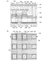
図9は、図1に示すメモリセルアレイ253が有する第1のトランジスタ211、及び第
2のトランジスタ212、または図4に示すメモリセルアレイ353が有する第1のトラ
ンジスタ311、及び第2のトランジスタ312に対応する半導体装置の構成の一例であ
る。図9(A)には、半導体装置の断面を、図9(B)には、半導体装置の平面を、それ
ぞれ示す。ここで、図9(A)は、図9(B)のA1−A2における断面に相当する。な
お、図9(B)では、煩雑になることを避けるため、当該半導体装置の構成要素の一部(
絶縁層154、絶縁層172、配線171、及び配線158)を省略している。図9(A
)および図9(B)に示される半導体装置は、下部に第1の半導体材料を用いたトランジ
スタ160を有し、上部に第2の半導体材料を用いたトランジスタ162を有するもので
ある。
<Cross-sectional configuration and planar configuration of semiconductor device>
9 corresponds to the
The insulating
The semiconductor device shown in FIG. 9B includes a
なお、トランジスタ160が、第1のトランジスタ211、及び第1のトランジスタ31
1と対応し、トランジスタ162が、第2のトランジスタ212、及び第2のトランジス
タ312と対応する。また、トランジスタ160、トランジスタ162、及び容量素子1
64により、メモリセル190が構成されている。
Note that the
1, the
64 constitutes a
ここで、第1の半導体材料と第2の半導体材料とは異なる材料とすることが望ましい。例
えば、第1の半導体材料を酸化物半導体以外の半導体材料(シリコンなど)とし、第2の
半導体材料を酸化物半導体とすることができる。酸化物半導体以外の材料を用いたトラン
ジスタは、高速動作が容易である。一方で、酸化物半導体を用いたトランジスタは、その
特性により長時間の電荷保持を可能とする。
Here, the first semiconductor material and the second semiconductor material are preferably different materials. For example, the first semiconductor material can be a semiconductor material other than an oxide semiconductor (such as silicon), and the second semiconductor material can be an oxide semiconductor. A transistor including a material other than an oxide semiconductor can easily operate at high speed. On the other hand, a transistor including an oxide semiconductor can hold charge for a long time due to its characteristics.
なお、上記トランジスタは、いずれもnチャネル型トランジスタであるものとして説明す
るが、pチャネル型トランジスタを用いることができるのはいうまでもない。また、開示
する発明の技術的な本質は、情報を保持するために酸化物半導体のようなオフ電流を十分
に低減することが可能な半導体材料をトランジスタ162に用いる点にあるから、半導体
装置に用いられる材料や半導体装置の構造など、半導体装置の具体的な構成をここで示す
ものに限定する必要はない。
Note that although all the above transistors are described as n-channel transistors, it goes without saying that p-channel transistors can be used. The technical essence of the disclosed invention is that a semiconductor material such as an oxide semiconductor that can sufficiently reduce off-state current is used for the
図9(A)および図9(B)におけるトランジスタ160は、半導体材料(例えば、シリ
コンなど)を含む基板100に設けられたチャネル形成領域116を挟むように設けられ
た不純物領域120aおよび不純物領域120bと、不純物領域120aおよび不純物領
域120bに接する金属化合物領域124aおよび金属化合物領域124bと、チャネル
形成領域116上に設けられたゲート絶縁層108と、ゲート絶縁層108上に設けられ
たゲート電極110と、を有する。なお、図9(A)のように、明示的にはソース電極や
ドレイン電極を有しない場合があるが、便宜上、このような状態を含めてトランジスタと
呼ぶ場合がある。また、この場合、トランジスタの接続関係を説明するために、ソース領
域やドレイン領域を含めてソース電極やドレイン電極と表現することがある。つまり、本
明細書において、ソース電極との記載には、ソース領域が、ドレイン電極との記載にはド
レイン領域が、含まれうる。
The
また、基板100上にはトランジスタ160を囲むように素子分離絶縁層106が設けら
れており、トランジスタ160を覆うように絶縁層128が設けられている。なお、高集
積化を実現するためには、図9(A)および図9(B)に示すようにトランジスタ160
がサイドウォール絶縁層を有しない構成とすることが望ましい。一方で、トランジスタ1
60の特性を重視する場合には、ゲート電極110の側面にサイドウォール絶縁層を設け
、不純物濃度が異なる領域を設けても良い。
An element
However, it is desirable that the structure does not have a sidewall insulating layer. On the other hand,
When importance is attached to the characteristics of 60, a sidewall insulating layer may be provided on the side surface of the
ここで、絶縁層128は、平坦性の良好な表面を有しているのが好ましく、例えば、絶縁
層128の表面は、二乗平均平方根(RMS)粗さを1nm以下とすることが好ましい。
Here, the insulating
図9(A)および図9(B)におけるトランジスタ162は、絶縁層128上に形成され
た絶縁層140に埋め込まれたソース電極142aおよびドレイン電極142bと、絶縁
層140、ソース電極142aおよびドレイン電極142bの一部と接する酸化物半導体
層144と、酸化物半導体層144を覆うゲート絶縁層146と、ゲート絶縁層146上
に酸化物半導体層144と重畳するように設けられたゲート電極148と、を有する。
A
ここで、酸化物半導体層144は水素などの不純物が十分に除去されることにより、また
は、十分な酸素が供給されることにより、高純度化されたものであることが望ましい。具
体的には、例えば、酸化物半導体層144の水素濃度は5×10¹⁹atoms/cm3
以下、望ましくは5×10¹⁸atoms/cm3以下、より望ましくは5×1017a
toms/cm3以下とする。なお、上述の酸化物半導体層144中の水素濃度は、二次
イオン質量分析法(SIMS:Secondary Ion Mass Spectro
scopy)で測定されるものである。このように、水素濃度が十分に低減されて高純度
化され、十分な酸素の供給により酸素欠損に起因するエネルギーギャップ中の欠陥準位が
低減された酸化物半導体層144では、水素等のドナーに起因するキャリア密度が1×1
012/cm3未満、望ましくは、1×1011/cm3未満、より望ましくは1.45
×1010/cm3未満となる。また、例えば、室温(25℃)でのオフ電流(ここでは
、単位チャネル幅(1μm)あたりの値)は100zA(1zA(ゼプトアンペア)は1
×10−21A)以下、望ましくは10zA以下となる。このように、i型化(真性化)
または実質的にi型化された酸化物半導体を用いることで、極めて優れたオフ電流特性の
トランジスタ162を得ることができる。
Here, it is preferable that the
Hereinafter, preferably 5 × 10 18 atoms / cm 3 or less, more preferably 5 × 10 17 a
toms / cm 3 or less. Note that the hydrogen concentration in the above-described
(scope). As described above, in the
Less than 0 12 / cm 3 , desirably less than 1 × 10 11 / cm 3 , more desirably 1.45
× 10 10 / cm 3 Further, for example, an off-current at room temperature (25 ° C.) (here, a value per unit channel width (1 μm)) is 100 zA (1 zA (zeptoampere) is 1.
× 10 −21 A) or less, preferably 10 zA or less. In this way, i-type (intrinsic)
Alternatively, by using a substantially i-type oxide semiconductor, the
また、絶縁層140の表面であって酸化物半導体層144と接する領域は、その二乗平均
平方根(RMS)粗さを1nm以下とすることが好ましい。このように、二乗平均平方根
(RMS)粗さが1nm以下という極めて平坦な領域にトランジスタ162のチャネル形
成領域を設けることにより、トランジスタ162が微細化される状況においても、短チャ
ネル効果などの不具合を防止し、良好な特性を有するトランジスタ162を提供すること
が可能である。
Further, it is preferable that the surface of the insulating
トランジスタ162の上には、絶縁層150が設けられており、絶縁層150および容量
素子164の電極152上には絶縁層154が設けられている。絶縁層150及び絶縁層
154にはゲート電極148に達する開口が形成され、該開口には電極170が形成され
ている。絶縁層154上に、絶縁層154に埋め込まれるように形成された電極170に
接して配線171を形成することで、ゲート電極148と配線171とが電気的に接続し
ている。絶縁層154及び配線171上には絶縁層172が設けられている。
An insulating
ゲート絶縁層146、絶縁層150、絶縁層154、及び絶縁層172に形成された開口
には、電極156が設けられ、絶縁層172上には電極156と接続する配線158が形
成される。ゲート絶縁層146、絶縁層150、絶縁層154、及び絶縁層172に形成
された開口に設けられた電極156と、絶縁層140に埋め込まれたドレイン電極142
bと、絶縁層128に埋め込まれた電極126と、を介して配線158とトランジスタ1
60のドレイン領域として機能する金属化合物領域124bとが電気的に接続される。
An
b and the
The
なお、開示する発明に係る半導体装置の構成は、図9(A)および図9(B)に示される
ものに限定されない。開示する発明の一態様の技術的思想は、酸化物半導体と、酸化物半
導体以外の材料と、を用いた積層構造を形成する点にあるから、電極の接続関係等の詳細
については、適宜変更することができる。
Note that the structure of the semiconductor device according to the disclosed invention is not limited to that illustrated in FIGS. 9A and 9B. Since the technical idea of one embodiment of the disclosed invention is to form a stacked structure using an oxide semiconductor and a material other than the oxide semiconductor, details of electrode connection relations and the like are changed as appropriate. can do.
次に、上記半導体装置の作製方法の一例について説明する。以下では、はじめに下部のト
ランジスタ160の作製方法について図10および図11を参照して説明し、その後、上
部のトランジスタ162および容量素子164の作製方法について図12および図13を
参照して説明する。
Next, an example of a method for manufacturing the semiconductor device will be described. In the following, a method for manufacturing the
まず、半導体材料を含む基板100を用意する(図10(A)参照)。半導体材料を含む
基板100としては、シリコンや炭化シリコンなどの単結晶半導体基板、多結晶半導体基
板、シリコンゲルマニウムなどの化合物半導体基板、SOI基板などを適用することがで
きる。なお、一般に「SOI基板」は、絶縁表面上にシリコン半導体層が設けられた構成
の基板をいうが、本明細書等においては、絶縁表面上にシリコン以外の材料からなる半導
体層が設けられた構成の基板も含む概念として用いる。つまり、「SOI基板」が有する
半導体層は、シリコン半導体層に限定されない。また、SOI基板には、ガラス基板など
の絶縁基板上に絶縁層を介して半導体層が設けられた構成のものが含まれるものとする。
First, the
ここでは、半導体材料を含む基板100として、単結晶シリコン基板を用いる場合の一例
について示すものとする。半導体材料を含む基板100として、特に、シリコンなどの単
結晶半導体基板を用いる場合には、半導体装置の読み出し動作を高速化することができる
ため好適である。
Here, an example in which a single crystal silicon substrate is used as the
なお、トランジスタのしきい値電圧を制御するために、後にトランジスタ160のチャネ
ル形成領域116となる領域に、不純物元素を添加しても良い。ここでは、トランジスタ
160のしきい値電圧が正となるように導電性を付与する不純物元素を添加する。半導体
材料がシリコンの場合、該導電性を付与する不純物には、例えば、硼素、アルミニウム、
ガリウムなどがある。なお、不純物元素の添加後には、加熱処理を行い、不純物元素の活
性化や不純物元素の添加時に生じる欠陥の改善等を図るのが望ましい。
Note that an impurity element may be added to a region which later becomes the
There is gallium. Note that after the impurity element is added, heat treatment is preferably performed to activate the impurity element or improve defects generated when the impurity element is added.
基板100上には、素子分離絶縁層を形成するためのマスクとなる保護層102を形成す
る(図10(A)参照)。保護層102としては、例えば、酸化シリコンや窒化シリコン
、酸窒化シリコンなどを材料とする絶縁層を用いることができる。
A
次に、上記の保護層102をマスクとしてエッチングを行い、保護層102に覆われてい
ない領域(露出している領域)の、基板100の一部を除去する。これにより他の半導体
領域と分離された半導体領域104が形成される(図10(B)参照)。当該エッチング
には、ドライエッチングを用いるのが好適であるが、ウェットエッチングを用いても良い
。エッチングガスやエッチング液については被エッチング材料に応じて適宜選択すること
ができる。
Next, etching is performed using the
次に、半導体領域104を覆うように絶縁層を形成し、半導体領域104に重畳する領域
の絶縁層を選択的に除去することで、素子分離絶縁層106を形成する(図10(C)参
照)。当該絶縁層は、酸化シリコンや窒化シリコン、酸窒化シリコンなどを用いて形成さ
れる。絶縁層の除去方法としては、CMP(化学的機械的研磨)処理などの研磨処理やエ
ッチング処理などがあるが、そのいずれを用いても良い。なお、半導体領域104の形成
後、または、素子分離絶縁層106の形成後には、上記保護層102を除去する。
Next, an insulating layer is formed so as to cover the
次に、半導体領域104の表面に絶縁層を形成し、当該絶縁層上に導電材料を含む層を形
成する。
Next, an insulating layer is formed on the surface of the
絶縁層は後のゲート絶縁層となるものであり、例えば、半導体領域104表面の熱処理(
熱酸化処理や熱窒化処理など)によって形成することができる。熱処理に代えて、高密度
プラズマ処理を適用しても良い。高密度プラズマ処理は、例えば、He、Ar、Kr、X
eなどの希ガス、酸素、酸化窒素、アンモニア、窒素、水素などの混合ガスを用いて行う
ことができる。もちろん、CVD法やスパッタリング法等を用いて絶縁層を形成しても良
い。当該絶縁層は、酸化シリコン、酸窒化シリコン、窒化シリコン、酸化ハフニウム、酸
化アルミニウム、酸化タンタル、酸化イットリウム、ハフニウムシリケート(HfSix
Oy(x>0、y>0))、窒素が添加されたハフニウムシリケート(HfSixOy(
x>0、y>0))、窒素が添加されたハフニウムアルミネート(HfAlxOy(x>
0、y>0))等を含む単層構造または積層構造とすることが望ましい。また、絶縁層の
厚さは、例えば、1nm以上100nm以下、好ましくは10nm以上50nm以下とす
ることができる。
The insulating layer will be a gate insulating layer later. For example, the surface of the
For example, thermal oxidation treatment or thermal nitridation treatment. Instead of heat treatment, high-density plasma treatment may be applied. For example, the high density plasma treatment may be He, Ar, Kr, X
This can be performed using a rare gas such as e, or a mixed gas of oxygen, nitrogen oxide, ammonia, nitrogen, hydrogen, or the like. Needless to say, the insulating layer may be formed by a CVD method, a sputtering method, or the like. The insulating layer includes silicon oxide, silicon oxynitride, silicon nitride, hafnium oxide, aluminum oxide, tantalum oxide, yttrium oxide, and hafnium silicate (HfSix
Oy (x> 0, y> 0)), hafnium silicate with nitrogen added (HfSixOy (
x> 0, y> 0)), nitrogen-added hafnium aluminate (HfAlxOy (x>
It is desirable to have a single layer structure or a stacked structure including 0, y> 0)). The insulating layer can have a thickness of, for example, 1 nm to 100 nm, preferably 10 nm to 50 nm.
導電材料を含む層は、アルミニウムや銅、チタン、タンタル、タングステン等の金属材料
を用いて形成することができる。また、多結晶シリコンなどの半導体材料を用いて、導電
材料を含む層を形成しても良い。形成方法も特に限定されず、蒸着法、CVD法、スパッ
タリング法、スピンコート法などの各種成膜方法を用いることができる。なお、本実施の
形態では、導電材料を含む層を、金属材料を用いて形成する場合の一例について示すもの
とする。
The layer including a conductive material can be formed using a metal material such as aluminum, copper, titanium, tantalum, or tungsten. Alternatively, a layer including a conductive material may be formed using a semiconductor material such as polycrystalline silicon. There is no particular limitation on the formation method, and various film formation methods such as an evaporation method, a CVD method, a sputtering method, and a spin coating method can be used. Note that in this embodiment, an example of the case where the layer including a conductive material is formed using a metal material is described.
その後、絶縁層および導電材料を含む層を選択的にエッチングして、ゲート絶縁層108
およびゲート電極110を形成する(図10(C)参照)。
After that, the
Then, the
次に、半導体領域104にリン(P)やヒ素(As)などを添加して、チャネル形成領域
116、不純物領域120a、及び不純物領域120bを形成する(図10(D)参照)
。なお、ここではn型トランジスタを形成するためにリンやヒ素を添加しているが、p型
トランジスタを形成する場合には、硼素(B)やアルミニウム(Al)などの不純物元素
を添加すればよい。ここで、添加する不純物の濃度は適宜設定することができるが、半導
体素子が高度に微細化される場合には、その濃度を高くすることが望ましい。
Next, phosphorus (P), arsenic (As), or the like is added to the
. Here, phosphorus or arsenic is added to form an n-type transistor. However, when a p-type transistor is formed, an impurity element such as boron (B) or aluminum (Al) may be added. . Here, the concentration of the impurity to be added can be set as appropriate. However, when the semiconductor element is highly miniaturized, it is desirable to increase the concentration.
なお、ゲート電極110の周囲にサイドウォール絶縁層を形成して、不純物元素が異なる
濃度で添加された不純物領域を形成しても良い。
Note that a sidewall insulating layer may be formed around the
次に、ゲート電極110、不純物領域120a、及び不純物領域120bを覆うように金
属層122を形成する(図11(A)参照)。当該金属層122は、真空蒸着法やスパッ
タリング法、スピンコート法などの各種成膜方法を用いて形成することができる。金属層
122は、半導体領域104を構成する半導体材料と反応することによって低抵抗な金属
化合物となる金属材料を用いて形成することが望ましい。このような金属材料としては、
例えば、チタン、タンタル、タングステン、ニッケル、コバルト、白金等がある。
Next, a
For example, there are titanium, tantalum, tungsten, nickel, cobalt, platinum, and the like.
次に、熱処理を施して、上記金属層122と半導体材料とを反応させる。これにより、不
純物領域120a、不純物領域120bに接する金属化合物領域124a、及び金属化合
物領域124bが形成される(図11(A)参照)。なお、ゲート電極110として多結
晶シリコンなどを用いる場合には、ゲート電極110の金属層122と接触する部分にも
、金属化合物領域が形成されることになる。
Next, heat treatment is performed to react the
上記熱処理としては、例えば、フラッシュランプの照射による熱処理を用いることができ
る。もちろん、その他の熱処理方法を用いても良いが、金属化合物の形成に係る化学反応
の制御性を向上させるためには、ごく短時間の熱処理を実現できる方法を用いることが望
ましい。なお、上記の金属化合物領域は、金属材料と半導体材料との反応により形成され
るものであり、十分に導電性が高められた領域である。当該金属化合物領域を形成するこ
とで、電気抵抗を十分に低減し、素子特性を向上させることができる。なお、金属化合物
領域124a、及び金属化合物領域124bを形成した後には、金属層122は除去する
。
As the heat treatment, for example, heat treatment by flash lamp irradiation can be used. Of course, other heat treatment methods may be used, but in order to improve the controllability of the chemical reaction related to the formation of the metal compound, it is desirable to use a method capable of realizing a heat treatment for a very short time. Note that the metal compound region is formed by a reaction between a metal material and a semiconductor material, and is a region in which conductivity is sufficiently increased. By forming the metal compound region, the electrical resistance can be sufficiently reduced and the device characteristics can be improved. Note that the
次に、トランジスタ160の金属化合物領域124b上に接するように電極126を形成
する(図11(B)参照)。電極126は、スパッタリング法をはじめとするPVD法や
、プラズマCVD法などのCVD法を用いて導電層を形成した後、当該導電層を所望の形
状にエッチング加工することによって形成される。また、導電層の材料としては、アルミ
ニウム、クロム、銅、タンタル、チタン、モリブデン、タングステンから選ばれた元素や
、上述した元素を成分とする合金等を用いることができる。マンガン、マグネシウム、ジ
ルコニウム、ベリリウム、ネオジム、スカンジウムのいずれか、またはこれらを複数組み
合わせた材料を用いてもよい。
Next, the
以上により、半導体材料を含む基板100を用いたトランジスタ160が形成される(図
11(B)参照)。このようなトランジスタ160は、高速動作が可能であるという特徴
を有する。このため、当該トランジスタを読み出し用のトランジスタとして用いることで
、情報の読み出しを高速に行うことができる。
Through the above steps, the
次に、上述の工程により形成された各構成を覆うように、絶縁層128を形成する(図1
1(C)参照)。絶縁層128は、酸化シリコン、酸窒化シリコン、窒化シリコン、酸化
アルミニウム等の無機絶縁材料を含む材料を用いて形成することができる。特に、絶縁層
128に誘電率の低い(low−k)材料を用いることで、各種電極や配線の重なりに起
因する容量を十分に低減することが可能になるため好ましい。なお、絶縁層128には、
これらの材料を用いた多孔性の絶縁層を適用しても良い。多孔性の絶縁層では、密度の高
い絶縁層と比較して誘電率が低下するため、電極や配線に起因する容量をさらに低減する
ことが可能である。また、絶縁層128は、ポリイミド、アクリル樹脂等の有機絶縁材料
を用いて形成することも可能である。なお、ここでは、絶縁層128を単層構造としてい
るが、開示する発明の一態様はこれに限定されない。絶縁層128を2層以上の積層構造
としても良い。
Next, an insulating
1 (C)). The insulating
A porous insulating layer using these materials may be applied. A porous insulating layer has a lower dielectric constant than an insulating layer having a high density, and thus it is possible to further reduce capacitance caused by electrodes and wiring. The insulating
その後、トランジスタ162および容量素子164の形成前の処理として、絶縁層128
にCMP処理を施して、ゲート電極110および電極126の上面を露出させる(図11
(D)参照)。ゲート電極110の上面を露出させる処理としては、CMP処理の他にエ
ッチング処理などを適用することも可能であるが、トランジスタ162の特性を向上させ
るために、絶縁層128の表面は可能な限り平坦にしておくことが望ましく、例えば、絶
縁層128の表面は、二乗平均平方根(RMS)粗さを1nm以下とすることが好ましい
。
After that, as a treatment before formation of the
CMP processing is performed to expose the upper surfaces of the
(See (D)). As a process for exposing the upper surface of the
なお、上記の各工程の前後には、さらに電極や配線、半導体層、絶縁層などを形成する工
程を含んでいても良い。例えば、配線の構造として、絶縁層および導電層の積層構造でな
る多層配線構造を採用して、高度に集積化した半導体装置を実現することも可能である。
Note that before and after each of the above steps, a step of forming an electrode, a wiring, a semiconductor layer, an insulating layer, or the like may be further included. For example, a highly integrated semiconductor device can be realized by adopting a multilayer wiring structure including a laminated structure of an insulating layer and a conductive layer as a wiring structure.
〈上部のトランジスタの作製方法〉
次に、ゲート電極110、電極126、絶縁層128などの上に導電層を形成し、該導電
層を選択的にエッチングして、ソース電極142a、ドレイン電極142bを形成する(
図12(A)参照)。
<Method for manufacturing upper transistor>
Next, a conductive layer is formed over the
(See FIG. 12A).
導電層は、スパッタリング法をはじめとするPVD法や、プラズマCVD法などのCVD
法を用いて形成することができる。また、導電層の材料としては、アルミニウム、クロム
、銅、タンタル、チタン、モリブデン、タングステンからから選ばれた元素や、上述した
元素を成分とする合金等を用いることができる。マンガン、マグネシウム、ジルコニウム
、ベリリウム、ネオジム、スカンジウムのいずれか、またはこれらを複数組み合わせた材
料を用いてもよい。
The conductive layer is formed by CVD such as PVD method such as sputtering method or plasma CVD method.
It can be formed using a method. As a material for the conductive layer, an element selected from aluminum, chromium, copper, tantalum, titanium, molybdenum, and tungsten, an alloy containing the above-described element as a component, or the like can be used. Any of manganese, magnesium, zirconium, beryllium, neodymium, scandium, or a combination of these may be used.
導電層は、単層構造であっても良いし、2層以上の積層構造としてもよい。例えば、チタ
ン膜や窒化チタン膜の単層構造、シリコンを含むアルミニウム膜の単層構造、アルミニウ
ム膜上にチタン膜が積層された2層構造、窒化チタン膜上にチタン膜が積層された2層構
造、チタン膜とアルミニウム膜とチタン膜とが積層された3層構造などが挙げられる。な
お、導電層を、チタン膜や窒化チタン膜の単層構造とする場合には、テーパー形状を有す
るソース電極142aおよびドレイン電極142bへの加工が容易であるというメリット
がある。
The conductive layer may have a single layer structure or a stacked structure of two or more layers. For example, a single-layer structure of a titanium film or a titanium nitride film, a single-layer structure of an aluminum film containing silicon, a two-layer structure in which a titanium film is laminated on an aluminum film, or a two-layer structure in which a titanium film is laminated on a titanium nitride film Examples of the structure include a three-layer structure in which a titanium film, an aluminum film, and a titanium film are stacked. Note that when the conductive layer has a single-layer structure of a titanium film or a titanium nitride film, there is an advantage that processing into the
また、導電層は、導電性の金属酸化物を用いて形成しても良い。導電性の金属酸化物とし
ては酸化インジウム(In2O3)、酸化スズ(SnO2)、酸化亜鉛(ZnO)、酸化
インジウム酸化スズ合金(In2O3−SnO2、ITOと略記する場合がある)、酸化
インジウム酸化亜鉛合金(In2O3−ZnO)、または、これらの金属酸化物材料にシ
リコン若しくは酸化シリコンを含有させたものを用いることができる。
The conductive layer may be formed using a conductive metal oxide. The conductive metal oxide may be abbreviated as indium oxide (In 2 O 3 ), tin oxide (SnO 2 ), zinc oxide (ZnO), indium oxide tin oxide alloy (In 2 O 3 —SnO 2 , ITO). Indium oxide zinc oxide alloy (In 2 O 3 —ZnO), or a metal oxide material containing silicon or silicon oxide can be used.
なお、導電層のエッチングは、ドライエッチング、ウェットエッチングのいずれを用いて
行っても良いが、微細化のためには、制御性の良いドライエッチングを用いるのが好適で
ある。また、形成されるソース電極142aおよびドレイン電極142bがテーパー形状
となるように行っても良い。テーパー角は、例えば、30°以上60°以下とすることが
できる。
Note that the etching of the conductive layer may be performed using either dry etching or wet etching, but it is preferable to use dry etching with good controllability for miniaturization. Alternatively, the
上部のトランジスタ162のチャネル長(L)は、ソース電極142a、およびドレイン
電極142bの上端部の間隔によって決定される。なお、チャネル長(L)が25nm未
満のトランジスタを形成する場合に用いるマスク形成の露光を行う際には、数nm〜数1
0nmと波長の短い超紫外線(Extreme Ultraviolet)を用いるのが
望ましい。超紫外線による露光は、解像度が高く焦点深度も大きい。従って、後に形成さ
れるトランジスタのチャネル長(L)を、2μm未満、好ましくは10nm以上350n
m(0.35μm)以下とすることも可能であり、回路の動作速度を高めることが可能で
ある。また、微細化によって、半導体装置の消費電力を低減することも可能である。
The channel length (L) of the
It is desirable to use Extreme Ultraviolet with a short wavelength of 0 nm. Exposure by extreme ultraviolet light has a high resolution and a large depth of focus. Therefore, the channel length (L) of a transistor to be formed later is less than 2 μm, preferably 10 nm or more and 350 n
m (0.35 μm) or less can be achieved, and the operation speed of the circuit can be increased. In addition, power consumption of the semiconductor device can be reduced by miniaturization.
なお、絶縁層128の上には、下地として機能する絶縁層を設けても良い。当該絶縁層は
、PVD法やCVD法などを用いて形成することができる。
Note that an insulating layer functioning as a base may be provided over the insulating
次に、ソース電極142a、およびドレイン電極142bを覆うように絶縁層140を形
成した後、ソース電極142aおよびドレイン電極142bが露出されるように、CMP
(化学的機械的研磨)処理によって絶縁層140を平坦化する(図12(A)参照)。
Next, after the insulating
The insulating
絶縁層140は、酸化シリコン、酸窒化シリコン、窒化シリコン、酸化アルミニウム等の
無機絶縁材料を含む材料を用いて形成することができる。絶縁層140には、後に酸化物
半導体層144が接することになるから、特に、酸化シリコンを用いたものにするのが好
適である。絶縁層140の形成方法に特に限定はないが、酸化物半導体層144と接する
ことを考慮すれば、水素が十分に低減された方法によって形成するのが望ましい。このよ
うな方法としては、例えば、スパッタリング法がある。もちろん、プラズマCVD法をは
じめとする他の成膜法を用いても良い。
The insulating
またCMP(化学的機械的研磨)処理は、ソース電極142aおよびドレイン電極142
bの表面の少なくとも一部が露出する条件で行う。また、当該CMP処理は、絶縁層14
0表面の二乗平均平方根(RMS)粗さが1nm以下(好ましくは0.5nm以下)とな
る条件で行うのが好ましい。このような条件でCMP処理を行うことにより、後に酸化物
半導体層144が形成される表面の平坦性を向上させ、トランジスタ162の特性を向上
させることができる。
In addition, the CMP (chemical mechanical polishing) process is performed using a
It is performed under the condition that at least a part of the surface of b is exposed. In addition, the CMP treatment is performed on the insulating layer 14.
It is preferable to carry out under the condition that the root mean square (RMS) roughness of the 0 surface is 1 nm or less (preferably 0.5 nm or less). By performing CMP treatment under such conditions, planarity of a surface over which the
なお、CMP処理は、1回のみ行ってもよいし、複数回行ってもよい。複数回に分けてC
MP処理を行う場合は、高い研磨レートの一次研磨を行った後、低い研磨レートの仕上げ
研磨を行うのが好ましい。このように研磨レートの異なる研磨を組み合わせることによっ
て、絶縁層140の表面の平坦性をさらに向上させることができる。
The CMP process may be performed only once or a plurality of times. C divided into multiple times
When performing MP treatment, it is preferable to perform final polishing at a low polishing rate after performing primary polishing at a high polishing rate. By combining polishing with different polishing rates in this way, the flatness of the surface of the insulating
次に、ソース電極142aの上面、ドレイン電極142bの上面、および絶縁層140の
上面に接するように酸化物半導体層を形成した後、当該酸化物半導体層を選択的にエッチ
ングして酸化物半導体層144を形成する。
Next, an oxide semiconductor layer is formed so as to be in contact with the upper surface of the
酸化物半導体層144は、四元系金属酸化物であるIn−Sn−Ga−Zn−O系や、三
元系金属酸化物であるIn−Ga−Zn−O系、In−Sn−Zn−O系、In−Al−
Zn−O系、Sn−Ga−Zn−O系、Al−Ga−Zn−O系、Sn−Al−Zn−O
系や、二元系金属酸化物であるIn−Zn−O系、Sn−Zn−O系、Al−Zn−O系
、Zn−Mg−O系、Sn−Mg−O系、In−Mg−O系や、In−O系、Sn−O系
、Zn−O系などを用いて形成することができる。また、上記酸化物半導体にSiO2を
含んでもよい。
The
Zn-O, Sn-Ga-Zn-O, Al-Ga-Zn-O, Sn-Al-Zn-O
In-Zn-O-based, Sn-Zn-O-based, Al-Zn-O-based, Zn-Mg-O-based, Sn-Mg-O-based, In-Mg--, which are binary metal oxides It can be formed using an O-based, In-O-based, Sn-O-based, Zn-O-based, or the like. Further, the oxide semiconductor may contain SiO 2 .
中でも、In−Ga−Zn−O系の酸化物半導体材料は、無電界時の抵抗が十分に高くオ
フ電流を十分に小さくすることが可能であり、また、電界効果移動度も高いため、半導体
装置に用いる半導体材料としては好適である。
Among them, an In—Ga—Zn—O-based oxide semiconductor material has a sufficiently high resistance when no electric field is applied and can have a sufficiently small off-state current. It is suitable as a semiconductor material used for the apparatus.
In−Ga−Zn−O系の酸化物半導体材料の代表例としては、InGaO3(ZnO)
m(m>0)で表記されるものがある。また、Gaに代えてMの表記を用い、InMO3
(ZnO)m(m>0)のように表記される酸化物半導体材料がある。ここで、Mは、ガ
リウム(Ga)、アルミニウム(Al)、鉄(Fe)、ニッケル(Ni)、マンガン(M
n)、コバルト(Co)などから選ばれた一の金属元素または複数の金属元素を示す。例
えば、Mとしては、Ga、GaおよびAl、GaおよびFe、GaおよびNi、Gaおよ
びMn、GaおよびCoなどを適用することができる。なお、上述の組成は結晶構造から
導き出されるものであり、あくまでも一例に過ぎないことを付記する。
As a typical example of the In—Ga—Zn—O-based oxide semiconductor material, InGaO 3 (ZnO)
Some are represented by m (m> 0). In addition, M is used instead of Ga, and InMO 3
There is an oxide semiconductor material represented as (ZnO) m (m> 0). Here, M is gallium (Ga), aluminum (Al), iron (Fe), nickel (Ni), manganese (M
n) One metal element or a plurality of metal elements selected from cobalt (Co) and the like. For example, as M, Ga, Ga and Al, Ga and Fe, Ga and Ni, Ga and Mn, Ga and Co, and the like can be applied. It should be noted that the above composition is derived from the crystal structure and is merely an example.
また、用いる酸化物半導体材料としては、少なくともインジウム(In)あるいは亜鉛(
Zn)とを含むことが好ましい。特にInとZnを含むことが好ましい。また、該酸化物
半導体材料を用いたトランジスタの電気特性のばらつきを減らすためのスタビライザーと
して、それらに加えてガリウム(Ga)を有することが好ましい。また、スタビライザー
としてスズ(Sn)を有することが好ましい。また、スタビライザーとしてハフニウム(
Hf)を有することが好ましい。また、スタビライザーとしてアルミニウム(Al)を有
することが好ましい。
As an oxide semiconductor material to be used, at least indium (In) or zinc (
Zn). In particular, In and Zn are preferably included. In addition to the stabilizer, gallium (Ga) is preferably used as a stabilizer for reducing variation in electrical characteristics of the transistor including the oxide semiconductor material. Moreover, it is preferable to have tin (Sn) as a stabilizer. Also, as a stabilizer, hafnium (
Hf) is preferred. Moreover, it is preferable to have aluminum (Al) as a stabilizer.
また、他のスタビライザーとして、ランタノイドである、ランタン(La)、セリウム(
Ce)、プラセオジム(Pr)、ネオジム(Nd)、サマリウム(Sm)、ユウロピウム
(Eu)、ガドリニウム(Gd)、テルビウム(Tb)、ジスプロシウム(Dy)、ホル
ミウム(Ho)、エルビウム(Er)、ツリウム(Tm)、イッテルビウム(Yb)、ル
テチウム(Lu)のいずれか一種あるいは複数種を有してもよい。
In addition, as other stabilizers, lanthanoids such as lanthanum (La), cerium (
Ce), praseodymium (Pr), neodymium (Nd), samarium (Sm), europium (Eu), gadolinium (Gd), terbium (Tb), dysprosium (Dy), holmium (Ho), erbium (Er), thulium ( Tm), ytterbium (Yb), or lutetium (Lu) may be used alone or in combination.
例えば、酸化物半導体として、酸化インジウム、酸化スズ、酸化亜鉛、二元系金属の酸化
物であるIn−Zn系酸化物、Sn−Zn系酸化物、Al−Zn系酸化物、Zn−Mg系
酸化物、Sn−Mg系酸化物、In−Mg系酸化物、In−Ga系酸化物、三元系金属の
酸化物であるIn−Ga−Zn系酸化物(IGZOとも表記する)、In−Al−Zn系
酸化物、In−Sn−Zn系酸化物、Sn−Ga−Zn系酸化物、Al−Ga−Zn系酸
化物、Sn−Al−Zn系酸化物、In−Hf−Zn系酸化物、In−La−Zn系酸化
物、In−Ce−Zn系酸化物、In−Pr−Zn系酸化物、In−Nd−Zn系酸化物
、In−Sm−Zn系酸化物、In−Eu−Zn系酸化物、In−Gd−Zn系酸化物、
In−Tb−Zn系酸化物、In−Dy−Zn系酸化物、In−Ho−Zn系酸化物、I
n−Er−Zn系酸化物、In−Tm−Zn系酸化物、In−Yb−Zn系酸化物、In
−Lu−Zn系酸化物、四元系金属の酸化物であるIn−Sn−Ga−Zn系酸化物、I
n−Hf−Ga−Zn系酸化物、In−Al−Ga−Zn系酸化物、In−Sn−Al−
Zn系酸化物、In−Sn−Hf−Zn系酸化物、In−Hf−Al−Zn系酸化物を用
いることができる。
For example, as an oxide semiconductor, indium oxide, tin oxide, zinc oxide, binary metal oxides such as In—Zn oxide, Sn—Zn oxide, Al—Zn oxide, Zn—Mg oxide Oxides, Sn—Mg oxides, In—Mg oxides, In—Ga oxides, In—Ga—Zn oxides (also referred to as IGZO) which are oxides of ternary metals, In— Al-Zn oxide, In-Sn-Zn oxide, Sn-Ga-Zn oxide, Al-Ga-Zn oxide, Sn-Al-Zn oxide, In-Hf-Zn oxide In-La-Zn-based oxide, In-Ce-Zn-based oxide, In-Pr-Zn-based oxide, In-Nd-Zn-based oxide, In-Sm-Zn-based oxide, In-Eu -Zn-based oxide, In-Gd-Zn-based oxide,
In-Tb-Zn-based oxide, In-Dy-Zn-based oxide, In-Ho-Zn-based oxide, I
n-Er-Zn-based oxide, In-Tm-Zn-based oxide, In-Yb-Zn-based oxide, In
-Lu-Zn-based oxide, In-Sn-Ga-Zn-based oxide which is an oxide of a quaternary metal, I
n-Hf-Ga-Zn-based oxide, In-Al-Ga-Zn-based oxide, In-Sn-Al-
A Zn-based oxide, an In-Sn-Hf-Zn-based oxide, or an In-Hf-Al-Zn-based oxide can be used.
なお、ここで、例えば、In−Ga−Zn系酸化物とは、InとGaとZnを有する酸化
物という意味であり、InとGaとZnの比率は問わない。また、InとGaとZn以外
の金属元素が入っていてもよい。
Note that here, for example, an In—Ga—Zn-based oxide means an oxide containing In, Ga, and Zn, and there is no limitation on the ratio of In, Ga, and Zn. Moreover, metal elements other than In, Ga, and Zn may be contained.
例えば、In:Ga:Zn=1:1:1(=1/3:1/3:1/3)あるいはIn:G
a:Zn=2:2:1(=2/5:2/5:1/5)の原子比のIn−Ga−Zn系酸化
物やその組成の近傍の酸化物を用いることができる。あるいは、In:Sn:Zn=1:
1:1(=1/3:1/3:1/3)、In:Sn:Zn=2:1:3(=1/3:1/
6:1/2)あるいはIn:Sn:Zn=2:1:5(=1/4:1/8:5/8)の原
子比のIn−Sn−Zn系酸化物やその組成の近傍の酸化物を用いるとよい。
For example, In: Ga: Zn = 1: 1: 1 (= 1/3: 1/3: 1/3) or In: G
An In—Ga—Zn-based oxide having an atomic ratio of a: Zn = 2: 2: 1 (= 2/5: 2/5: 1/5) or an oxide in the vicinity of the composition can be used. Alternatively, In: Sn: Zn = 1:
1: 1 (= 1/3: 1/3: 1/3), In: Sn: Zn = 2: 1: 3 (= 1/3: 1 /
6: 1/2) or In: Sn: Zn = 2: 1: 5 (= 1/4: 1/8: 5/8) atomic ratio of In—Sn—Zn-based oxide and the vicinity of its composition An oxide may be used.
しかし、これらに限られず、必要とする半導体特性(移動度、しきい値、ばらつき等)に
応じて適切な組成のものを用いればよい。また、必要とする半導体特性を得るために、キ
ャリア濃度や不純物濃度、欠陥密度、金属元素と酸素の原子数比、原子間結合距離、密度
等を適切なものとすることが好ましい。
However, the composition is not limited thereto, and a material having an appropriate composition may be used depending on required semiconductor characteristics (mobility, threshold value, variation, etc.). In order to obtain the required semiconductor characteristics, it is preferable that the carrier concentration, impurity concentration, defect density, atomic ratio of metal element to oxygen, interatomic bond distance, density, and the like are appropriate.
酸化物半導体層144をスパッタリング法で作製するための酸化物ターゲットとしては、
In:Ga:Zn=1:x:y(xは0以上、yは0.5以上5以下)の組成比で表され
るものを用いるのが好適である。例えば、In:Ga:Zn=1:1:1[atom比]
(x=1、y=1)、(すなわち、In2O3:Ga2O3:ZnO=1:1:2[mo
l数比])の組成比を有するターゲットなどを用いることができる。また、In:Ga:
Zn=1:1:0.5[atom比](x=1、y=0.5)の組成比を有するターゲッ
トや、In:Ga:Zn=1:1:2[atom比](x=1、y=2)の組成比を有す
るターゲットや、In:Ga:Zn=1:0:1[atom比](x=0、y=1)の組
成比を有するターゲットを用いることもできる。
As an oxide target for forming the
It is preferable to use one represented by a composition ratio of In: Ga: Zn = 1: x: y (x is 0 or more and y is 0.5 or more and 5 or less). For example, In: Ga: Zn = 1: 1: 1 [atom ratio]
(X = 1, y = 1) (that is, In 2 O 3 : Ga 2 O 3 : ZnO = 1: 1: 2 [mo
A target having a composition ratio of l number ratio]) can be used. In: Ga:
A target having a composition ratio of Zn = 1: 1: 0.5 [atom ratio] (x = 1, y = 0.5), In: Ga: Zn = 1: 1: 2 [atom ratio] (x = 1 and a target having a composition ratio of y = 2) and a target having a composition ratio of In: Ga: Zn = 1: 0: 1 [atom ratio] (x = 0, y = 1) can also be used.
本実施の形態では、非晶質構造の酸化物半導体層144を、In−Ga−Zn−O系の金
属酸化物ターゲットを用いるスパッタリング法により形成することとする。また、その膜
厚は、1nm以上50nm以下、好ましくは2nm以上20nm以下、より好ましくは3
nm以上15nm以下とする。
In this embodiment, the
It is set to not less than 15 nm and not more than 15 nm.
金属酸化物ターゲット中の金属酸化物の相対密度は80%以上、好ましくは95%以上、
さらに好ましくは99.9%以上である。相対密度の高い金属酸化物ターゲットを用いる
ことにより、緻密な構造の酸化物半導体層を形成することが可能である。
The relative density of the metal oxide in the metal oxide target is 80% or more, preferably 95% or more,
More preferably, it is 99.9% or more. By using a metal oxide target with a high relative density, an oxide semiconductor layer with a dense structure can be formed.
酸化物半導体層144の形成雰囲気は、希ガス(代表的にはアルゴン)雰囲気、酸素雰囲
気、または、希ガス(代表的にはアルゴン)と酸素との混合雰囲気とするのが好適である
。具体的には、例えば、水素、水、水酸基、水素化物などの不純物が、濃度1ppm以下
(望ましくは濃度10ppb以下)にまで除去された高純度ガス雰囲気を用いるのが好適
である。
The atmosphere in which the
酸化物半導体層144の形成の際には、例えば、減圧状態に保たれた処理室内に被処理物
を保持し、被処理物の温度が100℃以上550℃未満、好ましくは200℃以上400
℃以下となるように被処理物を熱する。または、酸化物半導体層144の形成の際の被処
理物の温度は、室温(25℃±10℃)としてもよい。そして、処理室内の水分を除去し
つつ、水素や水などが除去されたスパッタリングガスを導入し、上記ターゲットを用いて
酸化物半導体層144を形成する。被処理物を熱しながら酸化物半導体層144を形成す
ることにより、酸化物半導体層144に含まれる不純物を低減することができる。また、
スパッタリングによる損傷を軽減することができる。処理室内の水分を除去するためには
、吸着型の真空ポンプを用いることが好ましい。例えば、クライオポンプ、イオンポンプ
、チタンサブリメーションポンプなどを用いることができる。また、ターボ分子ポンプに
コールドトラップを加えたものを用いてもよい。クライオポンプなどを用いて排気するこ
とで、処理室から水素や水などを除去することができるため、酸化物半導体層中の不純物
濃度を低減できる。
When the
The object to be processed is heated so that the temperature is not higher than ° C. Alternatively, the temperature of the object to be processed when the
Damage due to sputtering can be reduced. In order to remove moisture in the processing chamber, an adsorption-type vacuum pump is preferably used. For example, a cryopump, an ion pump, a titanium sublimation pump, or the like can be used. Further, a turbo molecular pump provided with a cold trap may be used. By exhausting using a cryopump or the like, hydrogen, water, or the like can be removed from the treatment chamber, so that the impurity concentration in the oxide semiconductor layer can be reduced.
また、酸化物半導体層144は、上記水素や水などの不純物濃度の低減とともに、アルカ
リ金属、及びアルカリ土類金属の不純物濃度も低減させる必要がある。
The
なお、アルカリ金属は酸化物半導体を構成する元素ではないため、不純物である。アルカ
リ土類金属も、酸化物半導体を構成する元素ではない場合において、不純物となる。特に
、アルカリ金属のうちNaは、酸化物半導体膜に接する絶縁膜が酸化物である場合、当該
絶縁膜中に拡散してNa+となる。また、Naは、酸化物半導体膜内において、酸化物半
導体を構成する金属と酸素の結合を分断する、或いは、その結合中に割り込む。その結果
、例えば、閾値電圧がマイナス方向にシフトすることによるノーマリオン化、移動度の低
下等の、トランジスタの特性の劣化が起こり、加えて、特性のばらつきも生じる。この不
純物によりもたらされるトランジスタの特性の劣化と、特性のばらつきは、酸化物半導体
膜中の水素の濃度が十分に低い場合において顕著に現れる。従って、酸化物半導体膜中の
水素の濃度が5×1019cm−3以下、特に5×1018cm−3以下である場合には
、上記不純物の濃度を低減することが望ましい。具体的に、二次イオン質量分析法による
Na濃度の測定値は、5×10¹⁶/cm3以下、好ましくは1×1016/cm3以下
、更に好ましくは1×10¹⁵/cm3以下とするとよい。同様に、Li濃度の測定値は
、5×10¹⁵/cm3以下、好ましくは1×1015/cm3以下とするとよい。同様
に、K濃度の測定値は、5×10¹⁵/cm3以下、好ましくは1×1015/cm3以
下とするとよい。
Note that an alkali metal is an impurity because it is not an element included in an oxide semiconductor. Alkaline earth metal is also an impurity when it is not an element constituting an oxide semiconductor. In particular, Na in the alkali metal diffuses into the insulating film and becomes Na + when the insulating film in contact with the oxide semiconductor film is an oxide. In the oxide semiconductor film, Na breaks or interrupts the bond between the metal constituting the oxide semiconductor and oxygen. As a result, for example, the transistor characteristics are deteriorated such as normally-on due to the shift of the threshold voltage in the negative direction and the mobility is lowered. In addition, the characteristics are also varied. The deterioration of the characteristics of the transistor and the variation in characteristics caused by the impurities are conspicuous when the concentration of hydrogen in the oxide semiconductor film is sufficiently low. Therefore, when the concentration of hydrogen in the oxide semiconductor film is 5 × 10 19 cm −3 or less, particularly 5 × 10 18 cm −3 or less, it is desirable to reduce the concentration of the impurity. Specifically, the measured value of Na concentration by secondary ion mass spectrometry is 5 × 10 16 / cm 3 or less, preferably 1 × 10 16 / cm 3 or less, more preferably 1 × 10 15 / cm 3 or less. Good. Similarly, the measured value of the Li concentration is 5 × 10 15 / cm 3 or less, preferably 1 × 10 15 / cm 3 or less. Similarly, the measured value of the K concentration is 5 × 10 15 / cm 3 or less, preferably 1 × 10 15 / cm 3 or less.
次に、酸化物半導体層144の形成条件としては、例えば、被処理物とターゲットの間と
の距離が170mm、圧力が0.4Pa、直流(DC)電力が0.5kW、雰囲気が酸素
(酸素100%)雰囲気、またはアルゴン(アルゴン100%)雰囲気、または酸素とア
ルゴンの混合雰囲気、といった条件を適用することができる。なお、パルス直流(DC)
電源を用いると、ごみ(成膜時に形成される粉状の物質など)を低減でき、膜厚分布も均
一となるため好ましい。酸化物半導体層144の厚さは、前記の通り1nm以上50nm
以下、好ましくは2nm以上20nm以下、より好ましくは3nm以上15nm以下とす
る。開示する発明に係る構成を採用することで、このような厚さの酸化物半導体層144
を用いる場合であっても、微細化に伴う短チャネル効果を抑制することが可能である。た
だし、適用する酸化物半導体材料や、半導体装置の用途などにより適切な厚さは異なるか
ら、その厚さは、用いる材料や用途などに応じて選択することもできる。なお、上記のよ
うに絶縁層140を形成することにより、酸化物半導体層144のチャネル形成領域に相
当する部分の形成表面を十分に平坦化することができるので、厚みの小さい酸化物半導体
層であっても、好適に形成することが可能である。また、図12(B)に示すように、酸
化物半導体層144のチャネル形成領域に相当する部分の断面形状を、平坦な形状とする
ことが好ましい。酸化物半導体層144のチャネル形成領域に相当する部分の断面形状を
平坦な形状とすることすることにより、酸化物半導体層144の断面形状が平坦でない場
合と比較して、リーク電流を低減することができる。
Next, as a formation condition of the
It is preferable to use a power supply because dust (such as a powdery substance formed during film formation) can be reduced and the film thickness can be uniform. As described above, the thickness of the
Hereinafter, it is preferably 2 nm to 20 nm, more preferably 3 nm to 15 nm. By employing the structure according to the disclosed invention, the
Even in the case of using, it is possible to suppress the short channel effect associated with miniaturization. However, since the appropriate thickness differs depending on the oxide semiconductor material to be applied, the use of the semiconductor device, and the like, the thickness can also be selected according to the material, the use, and the like. Note that by forming the insulating
なお、酸化物半導体層144をスパッタリング法により形成する前には、アルゴンガスを
導入してプラズマを発生させる逆スパッタリングを行い、形成表面(例えば絶縁層140
の表面)の付着物を除去しても良い。ここで、逆スパッタリングとは、通常のスパッタリ
ングにおいては、スパッタターゲットにイオンを衝突させるところを、逆に、処理表面に
イオンを衝突させることによってその表面を改質する方法のことをいう。処理表面にイオ
ンを衝突させる方法としては、アルゴン雰囲気下で処理表面側に高周波電圧を印加して、
被処理物付近にプラズマを生成する方法などがある。なお、アルゴン雰囲気に代えて窒素
、ヘリウム、酸素などによる雰囲気を適用してもよい。
Note that before the
The surface adhering material may be removed. Here, the reverse sputtering refers to a method of modifying the surface by causing ions to collide with the treatment surface, instead of colliding ions with the sputtering target in normal sputtering. As a method of colliding ions with the treatment surface, a high frequency voltage is applied to the treatment surface side in an argon atmosphere,
There is a method of generating plasma in the vicinity of an object to be processed. Note that an atmosphere of nitrogen, helium, oxygen, or the like may be used instead of the argon atmosphere.
酸化物半導体層144の形成後には、酸化物半導体層144に対して熱処理(第1の熱処
理)を行うことが望ましい。この第1の熱処理によって酸化物半導体層144中の、過剰
な水素(水や水酸基を含む)を除去し、酸化物半導体層144の構造を整え、エネルギー
ギャップ中の欠陥準位を低減することができる。第1の熱処理の温度は、例えば、300
℃以上550℃未満、好ましくは400℃以上500℃以下とする。
After the
℃ ≧ 550 ℃, preferably ≧ 400 ℃.
熱処理は、例えば、抵抗発熱体などを用いた電気炉に被処理物を導入し、窒素雰囲気下、
450℃、1時間の条件で行うことができる。この間、酸化物半導体層は大気に触れさせ
ず、水や水素の混入が生じないようにする。
In the heat treatment, for example, an object to be processed is introduced into an electric furnace using a resistance heating element, and under a nitrogen atmosphere,
It can be performed at 450 ° C. for 1 hour. During this time, the oxide semiconductor layer is not exposed to the air so that water and hydrogen are not mixed.
熱処理装置は電気炉に限られず、加熱されたガスなどの媒体からの熱伝導、または熱輻射
によって、被処理物を加熱する装置を用いても良い。例えば、GRTA(Gas Rap
id Thermal Anneal)装置、LRTA(Lamp Rapid The
rmal Anneal)装置等のRTA(Rapid Thermal Anneal
)装置を用いることができる。LRTA装置は、ハロゲンランプ、メタルハライドランプ
、キセノンアークランプ、カーボンアークランプ、高圧ナトリウムランプ、高圧水銀ラン
プなどのランプから発する光(電磁波)の輻射により、被処理物を加熱する装置である。
GRTA装置は、高温のガスを用いて熱処理を行う装置である。ガスとしては、アルゴン
などの希ガス、または窒素のような、熱処理によって被処理物と反応しない不活性気体が
用いられる。
The heat treatment apparatus is not limited to an electric furnace, and an apparatus for heating an object to be processed by heat conduction or heat radiation from a medium such as a heated gas may be used. For example, GRTA (Gas Rap
id Thermal Anneal) device, LRTA (Lamp Rapid The
RTA (Rapid Thermal Anneal) equipment, etc.
) Device can be used. The LRTA apparatus is an apparatus that heats an object to be processed by radiation of light (electromagnetic waves) emitted from a lamp such as a halogen lamp, a metal halide lamp, a xenon arc lamp, a carbon arc lamp, a high pressure sodium lamp, or a high pressure mercury lamp.
The GRTA apparatus is an apparatus that performs heat treatment using a high-temperature gas. As the gas, an inert gas that does not react with an object to be processed by heat treatment, such as nitrogen or a rare gas such as argon, is used.
例えば、第1の熱処理として、熱せられた不活性ガス雰囲気中に被処理物を投入し、数分
間熱した後、当該不活性ガス雰囲気から被処理物を取り出すGRTA処理を行ってもよい
。GRTA処理を用いると短時間での高温熱処理が可能となる。また、被処理物の耐熱温
度を超える温度条件であっても適用が可能となる。なお、処理中に、不活性ガスを、酸素
を含むガスに切り替えても良い。酸素を含む雰囲気において第1の熱処理を行うことで、
酸素欠損に起因するエネルギーギャップ中の欠陥準位を低減することができるためである
。
For example, as the first heat treatment, a GRTA process may be performed in which an object to be processed is put in a heated inert gas atmosphere and heated for several minutes, and then the object to be processed is extracted from the inert gas atmosphere. When GRTA treatment is used, high-temperature heat treatment can be performed in a short time. In addition, application is possible even under temperature conditions exceeding the heat resistance temperature of the object to be processed. Note that the inert gas may be switched to a gas containing oxygen during the treatment. By performing the first heat treatment in an atmosphere containing oxygen,
This is because defect levels in the energy gap due to oxygen vacancies can be reduced.
なお、不活性ガス雰囲気としては、窒素、または希ガス(ヘリウム、ネオン、アルゴン等
)を主成分とする雰囲気であって、水、水素などが含まれない雰囲気を適用するのが望ま
しい。例えば、熱処理装置に導入する窒素や、ヘリウム、ネオン、アルゴン等の希ガスの
純度を、6N(99.9999%)以上、好ましくは7N(99.99999%)以上(
すなわち、不純物濃度が1ppm以下、好ましくは0.1ppm以下)とする。
Note that as the inert gas atmosphere, an atmosphere containing nitrogen or a rare gas (such as helium, neon, or argon) as a main component and not including water, hydrogen, or the like is preferably used. For example, the purity of nitrogen or a rare gas such as helium, neon, or argon introduced into the heat treatment apparatus is 6N (99.9999%) or more, preferably 7N (99.99999%) or more (
That is, the impurity concentration is 1 ppm or less, preferably 0.1 ppm or less.
いずれにしても、第1の熱処理によって不純物を低減し、酸素を供給し酸素欠損を補填し
て、i型(真性半導体)またはi型に限りなく近い酸化物半導体層を形成することで、極
めて優れた特性のトランジスタを実現することができる。
In any case, the first heat treatment reduces impurities, supplies oxygen, and compensates for oxygen vacancies, thereby forming an i-type (intrinsic semiconductor) or an oxide semiconductor layer that is almost as close to i-type as possible. A transistor with excellent characteristics can be realized.
ところで、上述の熱処理(第1の熱処理)には水素や水などを除去する効果があるから、
当該熱処理を、脱水化処理や、脱水素化処理などと呼ぶこともできる。当該脱水化処理や
、脱水素化処理は、酸化物半導体層144の形成後やゲート絶縁層146の形成後、ゲー
ト電極の形成後、などのタイミングにおいて行うことも可能である。また、このような脱
水化処理、脱水素化処理は、一回に限らず複数回行っても良い。
By the way, the above heat treatment (first heat treatment) has an effect of removing hydrogen, water, and the like.
This heat treatment can also be referred to as dehydration treatment, dehydrogenation treatment, or the like. The dehydration treatment or dehydrogenation treatment can be performed at the timing after the
酸化物半導体層144のエッチングは、上記熱処理の前、または上記熱処理の後のいずれ
において行っても良い。また、素子の微細化という観点からはドライエッチングを用いる
のが好適であるが、ウェットエッチングを用いても良い。エッチングガスやエッチング液
については被エッチング材料に応じて適宜選択することができる。なお、素子におけるリ
ークなどが問題とならない場合には、酸化物半導体層を島状に加工しないで用いても良い
。
The etching of the
酸化物半導体層144とソース電極142a、ドレイン電極142bとの間に、ソース領
域及びドレイン領域として機能する酸化物導電層をバッファ層として設けてもよい。
An oxide conductive layer functioning as a source region and a drain region may be provided as a buffer layer between the
酸化物導電層の成膜方法は、スパッタリング法や真空蒸着法(電子ビーム蒸着法など)や
、アーク放電イオンプレーティング法や、スプレー法を用いる。酸化物導電層の材料とし
ては、酸化亜鉛、酸化亜鉛アルミニウム、酸窒化亜鉛アルミニウム、酸化亜鉛ガリウムな
どを適用することができる。膜厚は50nm以上300nm以下の範囲内で適宜選択する
。また、上記材料に酸化珪素を含ませてもよい。
As a method for forming the oxide conductive layer, a sputtering method, a vacuum evaporation method (such as an electron beam evaporation method), an arc discharge ion plating method, or a spray method is used. As a material for the oxide conductive layer, zinc oxide, zinc aluminum oxide, zinc aluminum oxynitride, zinc gallium oxide, or the like can be used. The film thickness is appropriately selected within the range of 50 nm to 300 nm. Further, silicon oxide may be included in the above material.
酸化物導電層はソース電極142a、ドレイン電極142bと同じフォトリソグラフィ工
程によって形状を加工することができる。また、該酸化物導電層を、酸化物半導体層14
4を形成するためのフォトリソグラフィ工程においてさらに同じマスクによって形状を加
工してもよい。
The shape of the oxide conductive layer can be processed by the same photolithography process as that of the
In the photolithography process for forming 4, the shape may be further processed with the same mask.
ソース領域及びドレイン領域として、酸化物導電層を酸化物半導体層144とソース電極
142a、ドレイン電極142bとの間に設けることで、ソース領域及びドレイン領域の
低抵抗化を図ることができ、トランジスタ162の高速動作をすることができる。
By providing an oxide conductive layer as the source region and the drain region between the
また、酸化物半導体層144、酸化物導電層、ドレイン電極142bの構成とすることに
よって、トランジスタ162の耐圧を向上させることができる。
In addition, with the structure of the
ソース領域及びドレイン領域として酸化物導電層を用いることは、周辺回路(駆動回路)
の周波数特性を向上させるためにも有効である。金属電極(モリブデンやタングステン等
)と酸化物半導体層との接触に比べ、金属電極(モリブデンやタングステン等)と酸化物
導電層との接触は、接触抵抗を下げることができるからである。酸化物半導体層とソース
電極層及びドレイン電極層との間に酸化物導電層を介在させることで接触抵抗を低減でき
、周辺回路(駆動回路)の周波数特性を向上させることができる。
Using an oxide conductive layer as a source region and a drain region is a peripheral circuit (driving circuit).
It is also effective for improving the frequency characteristics of the. This is because contact resistance between the metal electrode (molybdenum, tungsten, or the like) and the oxide conductive layer can be reduced as compared with contact between the metal electrode (molybdenum, tungsten, or the like) and the oxide semiconductor layer. By interposing an oxide conductive layer between the oxide semiconductor layer and the source and drain electrode layers, contact resistance can be reduced, and frequency characteristics of the peripheral circuit (drive circuit) can be improved.
次に、酸化物半導体層144を覆うようにゲート絶縁層146を形成する(図12(B)
参照)。
Next, the
reference).
ゲート絶縁層146は、CVD法やスパッタリング法等を用いて形成することができる。
また、ゲート絶縁層146は、酸化シリコン、窒化シリコン、酸窒化シリコン、酸化アル
ミニウム、酸化タンタル、酸化ハフニウム、酸化イットリウム、ハフニウムシリケート(
HfSixOy(x>0、y>0))、窒素が添加されたハフニウムシリケート(HfS
ixOy(x>0、y>0))、窒素が添加されたハフニウムアルミネート(HfAlx
Oy(x>0、y>0))などを含むように形成するのが好適である。また、ゲート絶縁
層146は、単層構造としても良いし、積層構造としても良い。また、その厚さは特に限
定されないが、半導体装置を微細化する場合には、トランジスタの動作を確保するために
薄くするのが望ましい。例えば、酸化シリコンを用いる場合には、1nm以上100nm
以下、好ましくは10nm以上50nm以下とすることができる。
The
The
HfSixOy (x> 0, y> 0)), hafnium silicate added with nitrogen (HfS
ixOy (x> 0, y> 0)), nitrogen-added hafnium aluminate (HfAlx
Oy (x> 0, y> 0)) and the like are preferable. The
In the following, it is preferably 10 nm or more and 50 nm or less.
上述のように、ゲート絶縁層を薄くすると、トンネル効果などに起因するゲートリークが
問題となる。ゲートリークの問題を解消するには、ゲート絶縁層146に、酸化ハフニウ
ム、酸化タンタル、酸化イットリウム、ハフニウムシリケート(HfSixOy(x>0
、y>0))、窒素が添加されたハフニウムシリケート(HfSixOy(x>0、y>
0))、窒素が添加されたハフニウムアルミネート(HfAlxOy(x>0、y>0)
)、などの高誘電率(high−k)材料を用いると良い。high−k材料をゲート絶
縁層146に用いることで、電気的特性を確保しつつ、ゲートリークを抑制するために膜
厚を大きくすることが可能になる。例えば、酸化ハフニウムは比誘電率が15程度であり
、酸化シリコンの比誘電率の3〜4と比較して非常に大きな値を有している。このような
材料を用いることにより、酸化シリコン換算で15nm未満、好ましくは2nm以上10
nm以下のゲート絶縁層を実現することも容易になる。なお、high−k材料を含む膜
と、酸化シリコン、窒化シリコン、酸化窒化シリコン、窒化酸化シリコン、酸化アルミニ
ウムなどのいずれかを含む膜との積層構造としてもよい。
As described above, when the gate insulating layer is thin, gate leakage due to the tunnel effect or the like becomes a problem. In order to solve the problem of gate leakage, the
, Y> 0)), hafnium silicate doped with nitrogen (HfSixOy (x> 0, y>
0)), hafnium aluminate added with nitrogen (HfAlxOy (x> 0, y> 0)
), Etc., and a high dielectric constant (high-k) material may be used. By using a high-k material for the
It becomes easy to realize a gate insulating layer of nm or less. Note that a stacked structure of a film containing a high-k material and a film containing any of silicon oxide, silicon nitride, silicon oxynitride, silicon nitride oxide, aluminum oxide, and the like may be employed.
また、ゲート絶縁層146のように、酸化物半導体層144と接する膜には、酸化膜、窒
化膜、または金属酸化物膜を用いることが好ましく、例えば、酸化シリコン、窒化シリコ
ン、酸化窒化シリコン、窒化酸化シリコンなどの材料を用いて形成する。また、13族元
素および酸素を含む材料を用いて形成することもできる。13族元素および酸素を含む材
料としては、例えば、酸化ガリウム、酸化アルミニウム、酸化アルミニウムガリウムおよ
び酸化ガリウムアルミニウムのいずれか一または複数を含む材料などがある。ここで、酸
化アルミニウムガリウムとは、ガリウムの含有量(原子%)よりアルミニウムの含有量(
原子%)が多いものを示し、酸化ガリウムアルミニウムとは、ガリウムの含有量(原子%
)がアルミニウムの含有量(原子%)以上のものを示す。金属酸化物膜は、上述の材料を
用いて、単層構造または積層構造で形成することができる。
In addition, an oxide film, a nitride film, or a metal oxide film is preferably used as the film in contact with the
Gallium aluminum oxide is the content of gallium (atomic%)
) Indicates the aluminum content (atomic%) or more. The metal oxide film can be formed with a single-layer structure or a stacked structure by using the above materials.
ゲート絶縁層146の形成後には、不活性ガス雰囲気下、または酸素雰囲気下で第2の熱
処理を行うのが望ましい。熱処理の温度は、200℃以上450℃以下、望ましくは25
0℃以上350℃以下である。例えば、窒素雰囲気下で250℃、1時間の熱処理を行え
ばよい。第2の熱処理を行うことによって、トランジスタの電気的特性のばらつきを軽減
することができる。また、ゲート絶縁層146が酸素を含む場合、酸化物半導体層144
に酸素を供給し、該酸化物半導体層144の酸素欠損を補填して、i型(真性半導体)ま
たはi型に限りなく近い酸化物半導体層を形成することもできる。
After the
It is 0 degreeC or more and 350 degrees C or less. For example, heat treatment may be performed at 250 ° C. for 1 hour in a nitrogen atmosphere. By performing the second heat treatment, variation in electrical characteristics of the transistor can be reduced. In the case where the
Further, oxygen is supplied to the
なお、本実施の形態では、ゲート絶縁層146の形成後に第2の熱処理を行っているが、
第2の熱処理のタイミングはこれに限定されない。例えば、ゲート電極の形成後に第2の
熱処理を行っても良い。また、第1の熱処理に続けて第2の熱処理を行っても良いし、第
1の熱処理に第2の熱処理を兼ねさせても良いし、第2の熱処理に第1の熱処理を兼ねさ
せても良い。
Note that in this embodiment, the second heat treatment is performed after the
The timing of the second heat treatment is not limited to this. For example, the second heat treatment may be performed after the gate electrode is formed. The second heat treatment may be performed after the first heat treatment, the first heat treatment may be combined with the second heat treatment, or the second heat treatment may be combined with the first heat treatment. Also good.
上述のように、第1の熱処理と第2の熱処理の少なくとも一方を適用することで、酸化物
半導体層144を、その主成分以外の不純物が極力含まれないように高純度化することが
できる。
As described above, by applying at least one of the first heat treatment and the second heat treatment, the
次に、ゲート絶縁層146上にゲート電極148を形成する。
Next, the
ゲート電極148は、ゲート絶縁層146上に導電層を形成した後に、当該導電層を選択
的にエッチングすることによって形成することができる。ゲート電極148となる導電層
は、スパッタリング法をはじめとするPVD法や、プラズマCVD法などのCVD法を用
いて形成することができる。詳細は、ソース電極142aまたはドレイン電極142bな
どの場合と同様であり、これらの記載を参酌できる。
The
以上により、高純度化された酸化物半導体層144を用いたトランジスタ162が完成す
る(図12(C)参照)。このようなトランジスタ162は、オフ電流が十分低減されて
いるという特徴を有する。このため、当該トランジスタを書き込み用のトランジスタとし
て用いることで、長時間の電荷保持を行うことができる。
Through the above steps, the
次に、ゲート絶縁層146およびゲート電極148上に、絶縁層150を形成する(図1
2(D)参照)。絶縁層150は、PVD法やCVD法などを用いて形成することができ
る。また、酸化シリコン、酸窒化シリコン、窒化シリコン、酸化ハフニウム、酸化アルミ
ニウム等の無機絶縁材料を含む材料を用いて、単層または積層で形成することができる。
Next, the insulating
2 (D)). The insulating
なお、絶縁層150には、誘電率の低い材料や、誘電率の低い構造(多孔性の構造など)
を用いることが望ましい。絶縁層150の誘電率を低くすることにより、配線や電極など
の間に生じる容量を低減し、動作の高速化を図ることができるためである。
Note that the insulating
It is desirable to use This is because by reducing the dielectric constant of the insulating
次に、ソース電極142aと重畳するように、絶縁層150上に電極152を形成する(
図13(A)参照)。電極152は、ゲート電極148と同様の方法および材料で形成す
ることができるので、詳細は、上記ゲート電極148の記載を参酌することができる。以
上により、容量素子164が完成する。
Next, the
(See FIG. 13A). Since the
次に、絶縁層150および電極152上に、絶縁層154を形成する。絶縁層150、絶
縁層154に、ゲート電極148にまで達する開口を形成した後、開口に電極170を形
成し、絶縁層154上に、電極170に接する配線171を形成する(図13(B)参照
)。当該開口の形成は、マスクなどを用いた選択的なエッチングにより行われる。
Next, the insulating
次に、絶縁層154および配線171上に、絶縁層172を形成する。次に、ゲート絶縁
層146、絶縁層150、絶縁層154、および絶縁層172に、ドレイン電極142b
にまで達する開口を形成した後、開口に電極156を形成し、絶縁層172上に、電極1
56に接する配線158を形成する(図13(C)参照)。当該開口の形成は、マスクな
どを用いた選択的なエッチングにより行われる。
Next, the insulating
After forming an opening reaching up to, an
A
絶縁層154および絶縁層172は、絶縁層150と同様に、PVD法やCVD法などを
用いて形成することができる。また、酸化シリコン、酸窒化シリコン、窒化シリコン、酸
化ハフニウム、酸化アルミニウム等の無機絶縁材料を含む材料を用いて、単層または積層
で形成することができる。
The insulating
なお、絶縁層154および絶縁層172には、誘電率の低い材料や、誘電率の低い構造(
多孔性の構造など)を用いることが望ましい。絶縁層154および絶縁層172の誘電率
を低くすることにより、配線や電極などの間に生じる容量を低減し、動作の高速化を図る
ことができるためである。
Note that the insulating
It is desirable to use a porous structure. This is because by reducing the dielectric constants of the insulating
なお、上記絶縁層154および絶縁層172は、その表面が平坦になるように形成するこ
とが望ましい。表面が平坦になるように絶縁層154および絶縁層172を形成すること
で、半導体装置を微細化した場合などにおいても、絶縁層154および絶縁層172上に
、電極や配線などを好適に形成することができるためである。なお、絶縁層154および
絶縁層172の平坦化は、CMP(化学的機械的研磨)などの方法を用いて行うことがで
きる。
Note that the insulating
電極170および電極156は、例えば、開口を含む領域にPVD法やCVD法などを用
いて導電層を形成した後、エッチング処理やCMPといった方法を用いて、上記導電層の
一部を除去することにより形成することができる。
For example, the
より具体的には、例えば、開口を含む領域にPVD法によりチタン膜を薄く形成し、CV
D法により窒化チタン膜を薄く形成した後に、開口に埋め込むようにタングステン膜を形
成する方法を適用することができる。ここで、PVD法により形成されるチタン膜は、被
形成面の酸化膜(自然酸化膜など)を還元し、下部電極など(ここではドレイン電極14
2b)との接触抵抗を低減させる機能を有する。また、その後に形成される窒化チタン膜
は、導電性材料の拡散を抑制するバリア機能を備える。また、チタンや窒化チタンなどに
よるバリア膜を形成した後に、メッキ法により銅膜を形成してもよい。
More specifically, for example, a thin titanium film is formed by PVD in a region including the opening, and CV
A method of forming a tungsten film so as to be embedded in the opening after forming a thin titanium nitride film by the D method can be applied. Here, the titanium film formed by the PVD method reduces the oxide film (natural oxide film etc.) on the surface to be formed, and lower electrode etc.
2b) has a function of reducing contact resistance. The titanium nitride film formed thereafter has a barrier function that suppresses diffusion of the conductive material. Further, after forming a barrier film made of titanium, titanium nitride, or the like, a copper film may be formed by a plating method.
配線171および配線158は、スパッタリング法をはじめとするPVD法や、プラズマ
CVD法などのCVD法を用いて導電層を形成した後、当該導電層を所望の形状にエッチ
ング加工することによって形成される。また、導電層の材料としては、アルミニウム、ク
ロム、銅、タンタル、チタン、モリブデン、タングステンから選ばれた元素や、上述した
元素を成分とする合金等を用いることができる。マンガン、マグネシウム、ジルコニウム
、ベリリウム、ネオジム、スカンジウムのいずれか、またはこれらを複数組み合わせた材
料を用いてもよい。詳細は、ソース電極142aなどと同様である。
The
なお、上記工程の後に、各種配線や電極などを形成しても良い。配線や電極は、いわゆる
ダマシン法や、デュアルダマシン法などの方法を用いて形成することができる。
Note that various wirings, electrodes, and the like may be formed after the above steps. The wiring and the electrode can be formed using a so-called damascene method or a dual damascene method.
以上の工程より、図9(A)、図9(B)に示すような構成の半導体装置を作製すること
ができる。
Through the above steps, a semiconductor device having a structure illustrated in FIGS. 9A and 9B can be manufactured.
本実施の形態において示すトランジスタ162では、酸化物半導体層144が高純度化さ
れているため、その水素濃度は、5×10¹⁹atoms/cm3以下、望ましくは5×
1018atoms/cm3以下、より望ましくは5×1017atoms/cm3以下
である。また、酸化物半導体層144のキャリア密度は、一般的なシリコンウェハにおけ
るキャリア密度(1×10¹⁴/cm3程度)と比較して、十分に小さい値(例えば、1
×1012/cm3未満、より好ましくは、1.45×1010/cm3未満)をとる。
そして、トランジスタ162のオフ電流も十分に小さくなる。例えば、トランジスタ16
2の室温(25℃)でのオフ電流(ここでは、単位チャネル幅(1μm)あたりの値)は
100zA(1zA(ゼプトアンペア)は1×10⁻²¹A)以下、望ましくは10zA
以下となる。
In the
10 18 atoms / cm 3 or less, more desirably 5 × 10 17 atoms / cm 3 or less. In addition, the carrier density of the
× 10 12 / cm 3 , more preferably less than 1.45 × 10 10 / cm 3 ).
Then, the off-state current of the
The off current at room temperature (25 ° C.) of 2 (here, the value per unit channel width (1 μm)) is 100 zA (1 zA (zeptoampere) is 1 × 10 −21 A) or less, preferably 10 zA
It becomes as follows.
このように高純度化され、真性化された酸化物半導体層144を用いることで、トランジ
スタ162のオフ電流を十分に低減することが容易になる。そして、このようなトランジ
スタ162を用いることで、極めて長期にわたり記憶内容を保持することが可能な半導体
装置が得られる。
By using the highly purified and intrinsic
以上、本実施の形態に示す構成、方法などは、他の実施の形態に示す構成、方法などと適
宜組み合わせて用いることができる。
The structures, methods, and the like described in this embodiment can be combined as appropriate with any of the structures, methods, and the like described in the other embodiments.
(実施の形態4)
本実施の形態では、本明細書に開示する半導体装置に適用できるトランジスタの例を示す
。本明細書に開示する半導体装置に適用できるトランジスタの構造は特に限定されず、例
えばトップゲート構造、又はボトムゲート構造のスタガ型及びプレーナ型などを用いるこ
とができる。また、トランジスタはチャネル形成領域が一つ形成されるシングルゲート構
造でも、2つ形成されるダブルゲート構造もしくは3つ形成されるトリプルゲート構造で
あっても良い。また、チャネル領域の上下にゲート絶縁層を介して配置された2つのゲー
ト電極層を有する、デュアルゲート型でもよい。
(Embodiment 4)
In this embodiment, an example of a transistor that can be applied to the semiconductor device disclosed in this specification will be described. There is no particular limitation on the structure of the transistor that can be applied to the semiconductor device disclosed in this specification. For example, a top-gate structure or a staggered type or a planar type with a bottom gate structure can be used. The transistor may have a single gate structure in which one channel formation region is formed, a double gate structure in which two channel formation regions are formed, or a triple gate structure in which three channel formation regions are formed. Alternatively, a dual gate type having two gate electrode layers arranged above and below the channel region with a gate insulating layer interposed therebetween may be used.
本明細書に開示する半導体装置(例えば、実施の形態1におけるトランジスタ212)に
適用できるトランジスタの断面構造の例を図14(A)乃至(D)に示す。図14(A)
乃至(D)に示すトランジスタは絶縁層400上に設ける例を示すが、ガラス基板などの
基板上に設けられてもよい。
Examples of a cross-sectional structure of a transistor that can be applied to the semiconductor device disclosed in this specification (eg, the
The transistors illustrated in FIGS. 1 to 3D are provided over the insulating
図14(A)に示すトランジスタ410は、ボトムゲート構造の薄膜トランジスタの一つ
であり、逆スタガ型薄膜トランジスタともいう。
A
トランジスタ410は、絶縁層400上に、ゲート電極層401、ゲート絶縁層402、
酸化物半導体層403、ソース電極層405a、及びドレイン電極層405bを含む。ま
た、トランジスタ410を覆い、酸化物半導体層403に積層する絶縁層407が設けら
れている。絶縁層407上にはさらに絶縁層409が形成されている。
The
An
図14(B)に示すトランジスタ420は、チャネル保護型(チャネルストップ型ともい
う)と呼ばれるボトムゲート構造の一つであり逆スタガ型薄膜トランジスタともいう。
A
トランジスタ420は、絶縁層400上に、ゲート電極層401、ゲート絶縁層402、
酸化物半導体層403、酸化物半導体層403のチャネル形成領域を覆うチャネル保護層
として機能する絶縁層427、ソース電極層405a、及びドレイン電極層405bを含
む。また、トランジスタ420を覆い、絶縁層409が形成されている。
The
The
図14(C)示すトランジスタ430はボトムゲート型の薄膜トランジスタであり、絶縁
表面を有する基板である絶縁層400上に、ゲート電極層401、ゲート絶縁層402、
ソース電極層405a、ドレイン電極層405b、及び酸化物半導体層403を含む。ま
た、トランジスタ430を覆い、酸化物半導体層403に接する絶縁層407が設けられ
ている。絶縁層407上にはさらに絶縁層409が形成されている。
A
A
トランジスタ430においては、ゲート絶縁層402は絶縁層400及びゲート電極層4
01上に接して設けられ、ゲート絶縁層402上にソース電極層405a、ドレイン電極
層405bが接して設けられている。そして、ゲート絶縁層402、及びソース電極層4
05a、ドレイン電極層405b上に酸化物半導体層403が設けられている。
In the
The
05a. An
図14(D)に示すトランジスタ440は、トップゲート構造の薄膜トランジスタの一つ
である。トランジスタ440は、絶縁層400上に、絶縁層437、酸化物半導体層40
3、ソース電極層405a、及びドレイン電極層405b、ゲート絶縁層402、ゲート
電極層401を含み、ソース電極層405a、ドレイン電極層405bにそれぞれ配線層
436a、配線層436bが接して設けられ電気的に接続している。
A
3, the
ボトムゲート構造のトランジスタ410、420、430を基板上に設ける場合、下地膜
となる絶縁膜を絶縁層400とゲート電極層の間に設けてもよい。下地膜は、絶縁層40
0からの不純物元素の拡散を防止する機能があり、窒化シリコン膜、酸化シリコン膜、窒
化酸化シリコン膜、又は酸化窒化シリコン膜から選ばれた一又は複数の膜による積層構造
により形成することができる。
In the case where the
It has a function of preventing diffusion of impurity elements from 0, and can be formed with a stacked structure of one or more films selected from a silicon nitride film, a silicon oxide film, a silicon nitride oxide film, and a silicon oxynitride film. .
ゲート電極層401の材料は、モリブデン、チタン、クロム、タンタル、タングステン、
アルミニウム、銅、ネオジム、スカンジウム等の金属材料またはこれらを主成分とする合
金材料を用いて、単層でまたは積層して形成することができる。
The material of the
A single layer or stacked layers can be formed using a metal material such as aluminum, copper, neodymium, or scandium or an alloy material containing any of these as a main component.
ゲート絶縁層402は、プラズマCVD法又はスパッタリング法等を用いて、酸化シリコ
ン層、窒化シリコン層、酸化窒化シリコン層、窒化酸化シリコン層、酸化アルミニウム層
、窒化アルミニウム層、酸化窒化アルミニウム層、窒化酸化アルミニウム層、又は酸化ハ
フニウム層を単層で又は積層して形成することができる。例えば、第1のゲート絶縁層と
してプラズマCVD法により膜厚50nm以上200nm以下の窒化シリコン層(SiN
y(y>0))を形成し、第1のゲート絶縁層上に第2のゲート絶縁層として膜厚5nm
以上300nm以下の酸化シリコン層(SiOx(x>0))を積層して、合計膜厚20
0nmのゲート絶縁層とする。
The
y (y> 0)), and a film thickness of 5 nm is formed on the first gate insulating layer as the second gate insulating layer.
A silicon oxide layer (SiO x (x> 0)) having a thickness of 300 nm or less is stacked, and a total film thickness of 20
The gate insulating layer is 0 nm.
ソース電極層405a、ドレイン電極層405bに用いる導電膜としては、例えば、Al
、Cr、Cu、Ta、Ti、Mo、Wからから選ばれた元素、または上述した元素を成分
とする合金か、上述した元素を組み合わせた合金膜等を用いることができる。また、Al
、Cuなどの金属層の下側又は上側の一方または双方にTi、Mo、Wなどの高融点金属
層を積層させた構成としても良い。また、Al膜に生ずるヒロックやウィスカーの発生を
防止する元素(Si、Nd、Scなど)が添加されているAl材料を用いることで耐熱性
を向上させることが可能となる。
As a conductive film used for the
, Cr, Cu, Ta, Ti, Mo, W, an alloy containing the above-described element as a component, an alloy film combining the above-described elements, or the like can be used. Al
Further, a configuration may be adopted in which a refractory metal layer such as Ti, Mo, or W is laminated on one or both of the lower side or the upper side of a metal layer such as Cu. In addition, heat resistance can be improved by using an Al material to which an element (Si, Nd, Sc, or the like) that prevents generation of hillocks and whiskers generated in the Al film is used.
ソース電極層405a、ドレイン電極層405bに接続する配線層436a、配線層43
6bのような導電膜も、ソース電極層405a、ドレイン電極層405bと同様な材料を
用いることができる。
A
For the conductive film such as 6b, a material similar to that of the
また、ソース電極層405a、ドレイン電極層405b(これと同じ層で形成される配線
層を含む)となる導電膜としては導電性の金属酸化物で形成しても良い。導電性の金属酸
化物としては酸化インジウム(In2O3)、酸化スズ(SnO2)、酸化亜鉛(ZnO
)、酸化インジウム酸化スズ合金(In2O3―SnO2、ITOと略記する)、酸化イ
ンジウム酸化亜鉛合金(In2O3―ZnO)またはこれらの金属酸化物材料に酸化シリ
コンを含ませたものを用いることができる。
Alternatively, the conductive film to be the
), Indium oxide-tin oxide alloy (In 2 O 3 —SnO 2 , abbreviated as ITO), indium zinc oxide alloy (In 2 O 3 —ZnO), or a metal oxide material containing silicon oxide Can be used.
絶縁層407、絶縁層427、及び絶縁層437は、代表的には酸化シリコン膜、酸化窒
化シリコン膜、酸化アルミニウム膜、または酸化窒化アルミニウム膜などの無機絶縁膜を
用いることができる。
As the insulating
絶縁層409は、窒化シリコン膜、窒化アルミニウム膜、窒化酸化シリコン膜、窒化酸化
アルミニウム膜などの無機絶縁膜を用いることができる。
As the insulating
また、絶縁層409上にトランジスタ起因の表面凹凸を低減するために平坦化絶縁膜を形
成してもよい。平坦化絶縁膜としては、ポリイミド、アクリル樹脂、ベンゾシクロブテン
系樹脂、等の有機材料を用いることができる。また上記有機材料の他に、低誘電率材料(
low−k材料)等を用いることができる。なお、これらの材料で形成される絶縁膜を複
数積層させることで、平坦化絶縁膜を形成してもよい。
Further, a planarization insulating film may be formed over the insulating
low-k material) or the like. Note that the planarization insulating film may be formed by stacking a plurality of insulating films formed using these materials.
また、酸化物半導体層403とソース電極層405a、ドレイン電極層405bとの間に
、ソース領域及びドレイン領域として機能する酸化物導電層をバッファ層として設けても
よい。図14(D)のトランジスタ440に酸化物導電層を設けたトランジスタ441、
及びトランジスタ442を図15(A)(B)に示す。
Further, an oxide conductive layer functioning as a source region and a drain region may be provided as a buffer layer between the
A
図15(A)、及び図15(B)のトランジスタ441、トランジスタ442は、酸化物
半導体層403とソース電極層405a、ドレイン電極層405bとの間に、ソース領域
及びドレイン領域として機能する酸化物導電層404a、及び酸化物導電層404bが形
成されている。図15(A)、及び図15(B)のトランジスタ441、及びトランジス
タ442は作製工程により酸化物導電層404a、酸化物導電層404bの形状が異なる
例である。
The
図15(A)のトランジスタ441では、酸化物半導体膜と酸化物導電膜の積層を形成し
、酸化物半導体膜と酸化物導電膜との積層を同じフォトリソグラフィ工程によって形状を
加工して島状の酸化物半導体層403と酸化物導電膜を形成する。酸化物半導体層及び酸
化物導電膜上にソース電極層405a、ドレイン電極層405bを形成した後、ソース電
極層405a、ドレイン電極層405bをマスクとして、島状の酸化物導電膜をエッチン
グし、ソース領域およびドレイン領域となる酸化物導電層404a、および酸化物導電層
404bを形成する。
In the
図15(B)のトランジスタ442では、酸化物半導体層403上に酸化物導電膜を形成
し、その上に金属導電膜を形成し、酸化物導電膜および金属導電膜を同じフォトリソグラ
フィ工程によって加工して、酸化物導電層404a、酸化物導電層404b、ソース電極
層405a、およびドレイン電極層405bを形成する。
In the
なお、酸化物導電層の形状を加工するためのエッチング処理の際、酸化物半導体層が過剰
にエッチングされないように、エッチング条件(エッチング材の種類、濃度、エッチング
時間等)を適宜調整する。
Note that etching conditions (such as the type of etching material, concentration, and etching time) are adjusted as appropriate so that the oxide semiconductor layer is not excessively etched in the etching treatment for processing the shape of the oxide conductive layer.
酸化物導電層404a、および酸化物導電層404bの成膜方法は、スパッタリング法や
真空蒸着法(電子ビーム蒸着法など)や、アーク放電イオンプレーティング法や、スプレ
ー法を用いる。酸化物導電層の材料としては、酸化亜鉛、酸化亜鉛アルミニウム、酸窒化
亜鉛アルミニウム、酸化亜鉛ガリウムなどを適用することができる。また、上記材料に酸
化珪素を含ませてもよい。
As a method for forming the
ソース領域及びドレイン領域として、酸化物導電層を酸化物半導体層403とソース電極
層405a、ドレイン電極層405bとの間に設けることで、ソース領域及びドレイン領
域の低抵抗化を図ることができ、トランジスタ441、442が高速動作をすることがで
きる。
By providing an oxide conductive layer between the
また、酸化物半導体層403、酸化物導電層404a、および酸化物導電層404b、ソ
ース電極層405a、ドレイン電極層405bの構成とすることによって、トランジスタ
441、およびトランジスタ442の耐圧を向上させることができる。
In addition, with the structure of the
本実施の形態は、他の実施の形態に記載した構成と適宜組み合わせて実施することが可能
である。
This embodiment can be implemented in appropriate combination with the structures described in the other embodiments.
(実施の形態5)
上記実施の形態1乃至4において、トランジスタの半導体層に用いることのできる酸化物
半導体層の一形態を、図16を用いて説明する。
(Embodiment 5)
One embodiment of an oxide semiconductor layer that can be used for the semiconductor layers of the transistors in
本実施の形態の酸化物半導体層は、第1の結晶性酸化物半導体層上に第1の結晶性酸化物
半導体層よりも厚い第2の結晶性酸化物半導体層を有する積層構造である。
The oxide semiconductor layer in this embodiment has a stacked structure in which a second crystalline oxide semiconductor layer that is thicker than the first crystalline oxide semiconductor layer is provided over the first crystalline oxide semiconductor layer.
絶縁層400上に絶縁層437を形成する。本実施の形態では、絶縁層437として、P
CVD法またはスパッタリング法を用いて、50nm以上600nm以下の膜厚の酸化物
絶縁層を形成する。例えば、酸化シリコン膜、酸化ガリウム膜、酸化アルミニウム膜、酸
化窒化シリコン膜、酸化窒化アルミニウム膜、または窒化酸化シリコン膜から選ばれた一
層またはこれらの積層を用いることができる。
An insulating
An oxide insulating layer with a thickness greater than or equal to 50 nm and less than or equal to 600 nm is formed by a CVD method or a sputtering method. For example, a single layer selected from a silicon oxide film, a gallium oxide film, an aluminum oxide film, a silicon oxynitride film, an aluminum oxynitride film, or a silicon nitride oxide film, or a stacked layer thereof can be used.
次に、絶縁層437上に膜厚1nm以上10nm以下の第1の酸化物半導体膜を形成する
。第1の酸化物半導体膜の形成は、スパッタリング法を用い、そのスパッタリング法によ
る成膜時における基板温度は200℃以上400℃以下とする。
Next, a first oxide semiconductor film with a thickness of 1 nm to 10 nm is formed over the insulating
本実施の形態では、金属酸化物ターゲット(In−Ga−Zn−O系金属酸化物ターゲッ
ト(In2O3:Ga2O3:ZnO=1:1:2[mol数比])を用いて、基板とタ
ーゲットの間との距離を170mm、基板温度を250℃、圧力を0.4Pa、直流(D
C)電源を0.5kW、酸素のみ、アルゴンのみ、又はアルゴン及び酸素雰囲気下で膜厚
5nmの第1の酸化物半導体膜を成膜する。
In this embodiment, a metal oxide target (In—Ga—Zn—O-based metal oxide target (In 2 O 3 : Ga 2 O 3 : ZnO = 1: 1: 2 [molar ratio]) is used. The distance between the substrate and the target is 170 mm, the substrate temperature is 250 ° C., the pressure is 0.4 Pa, and the direct current (D
C) A first oxide semiconductor film having a thickness of 5 nm is formed with a power source of 0.5 kW and oxygen alone, argon alone, or an atmosphere of argon and oxygen.
次いで、基板を配置するチャンバー雰囲気を窒素、または乾燥空気とし、第1の加熱処理
を行う。第1の加熱処理の温度は、400℃以上750℃以下とする。第1の加熱処理に
よって第1の結晶性酸化物半導体層450aを形成する(図16(A)参照)。
Next, a first heat treatment is performed using nitrogen or dry air as a chamber atmosphere in which the substrate is placed. The temperature of the first heat treatment is 400 ° C. or higher and 750 ° C. or lower. The first crystalline
第1の加熱処理の温度にもよるが、第1の加熱処理によって、膜表面から結晶化が起こり
、膜の表面から内部に向かって結晶成長し、C軸配向した結晶が得られる。第1の加熱処
理によって、亜鉛と酸素が膜表面に多く集まり、上平面が六角形をなす亜鉛と酸素からな
るグラフェンタイプの二次元結晶が最表面に1層または複数層形成され、これが膜厚方向
に成長して重なり積層となる。加熱処理の温度を上げると表面から内部、そして内部から
底部と結晶成長が進行する。
Although it depends on the temperature of the first heat treatment, crystallization occurs from the surface of the film by the first heat treatment, crystal grows from the surface of the film toward the inside, and a C-axis oriented crystal is obtained. By the first heat treatment, a large amount of zinc and oxygen gathers on the film surface, and a graphene-type two-dimensional crystal composed of zinc and oxygen having a hexagonal upper surface is formed on the outermost surface. It grows in the direction and overlaps. When the temperature of the heat treatment is increased, crystal growth proceeds from the surface to the inside and from the inside to the bottom.
第1の加熱処理によって、酸化物絶縁層である絶縁層437中の酸素を第1の結晶性酸化
物半導体層450aとの界面またはその近傍(界面からプラスマイナス5nm)に拡散さ
せて、第1の結晶性酸化物半導体層の酸素欠損を低減する。従って、下地絶縁層として用
いられる絶縁層437は、膜中(バルク中)、第1の結晶性酸化物半導体層450aと絶
縁層437の界面、のいずれかには少なくとも化学量論比を超える量の酸素が存在するこ
とが好ましい。
By the first heat treatment, oxygen in the insulating
次いで、第1の結晶性酸化物半導体層450a上に10nmよりも厚い第2の酸化物半導
体膜を形成する。第2の酸化物半導体膜の形成は、スパッタリング法を用い、その成膜時
における基板温度は200℃以上400℃以下とする。成膜時における基板温度を200
℃以上400℃以下とすることにより、第1の結晶性酸化物半導体層の表面上に接して成
膜する酸化物半導体層にプリカーサの整列が起き、所謂、秩序性を持たせることができる
。
Next, a second oxide semiconductor film thicker than 10 nm is formed over the first crystalline
When the temperature is higher than or equal to 400 ° C. and lower than or equal to 400 ° C., precursor alignment occurs in the oxide semiconductor layer formed in contact with the surface of the first crystalline oxide semiconductor layer, and so-called ordering can be imparted.
本実施の形態では、金属酸化物ターゲット(In−Ga−Zn−O系金属酸化物ターゲッ
ト(In2O3:Ga2O3:ZnO=1:1:2[mol数比])を用いて、基板とタ
ーゲットの間との距離を170mm、基板温度を400℃、圧力を0.4Pa、直流(D
C)電源を0.5kW、酸素のみ、アルゴンのみ、又はアルゴン及び酸素雰囲気下で膜厚
25nmの第2の酸化物半導体膜を成膜する。
In this embodiment, a metal oxide target (In—Ga—Zn—O-based metal oxide target (In 2 O 3 : Ga 2 O 3 : ZnO = 1: 1: 2 [molar ratio]) is used. The distance between the substrate and the target is 170 mm, the substrate temperature is 400 ° C., the pressure is 0.4 Pa, and the direct current (D
C) A second oxide semiconductor film having a thickness of 25 nm is formed with a power source of 0.5 kW and oxygen alone, argon alone, or an atmosphere of argon and oxygen.
次いで、基板を配置するチャンバー雰囲気を窒素雰囲気下、酸素雰囲気下、或いは窒素と
酸素の混合雰囲気下とし、第2の加熱処理を行う。第2の加熱処理の温度は、400℃以
上750℃以下とする。第2の加熱処理によって第2の結晶性酸化物半導体層450bを
形成する(図16(B)参照)。第2の加熱処理は、窒素雰囲気下、酸素雰囲気下、或い
は窒素と酸素の混合雰囲気下で行うことにより、第2の結晶性酸化物半導体層450bの
高密度化及び欠陥数の減少を図る。第2の加熱処理によって、第1の結晶性酸化物半導体
層450aを核として膜厚方向、即ち底部から内部に結晶成長が進行して第2の結晶性酸
化物半導体層450bが形成される。
Next, a second heat treatment is performed with a chamber atmosphere in which the substrate is placed in a nitrogen atmosphere, an oxygen atmosphere, or a mixed atmosphere of nitrogen and oxygen. The temperature of the second heat treatment is 400 ° C to 750 ° C. The second crystalline
また、絶縁層437の形成から第2の加熱処理までの工程を大気に触れることなく連続的
に行うことが好ましい。絶縁層437の形成から第2の加熱処理までの工程は、水素及び
水分をほとんど含まない雰囲気(不活性雰囲気、減圧雰囲気、乾燥空気雰囲気など)下に
制御することが好ましく、例えば、水分については露点−40℃以下、好ましくは露点−
50℃以下の乾燥窒素雰囲気とする。
Further, it is preferable that steps from the formation of the insulating
A dry nitrogen atmosphere of 50 ° C. or lower is used.
次いで、第1の結晶性酸化物半導体層450aと第2の結晶性酸化物半導体層450bか
らなる酸化物半導体積層を加工して島状の酸化物半導体積層からなる酸化物半導体層45
3を形成する(図16(C)参照)。図では、第1の結晶性酸化物半導体層450aと第
2の結晶性酸化物半導体層450bの界面を点線で示し、酸化物半導体積層と説明してい
るが、明確な界面が存在しているのではなく、あくまで分かりやすく説明するために図示
している。
Next, the oxide semiconductor stack 45 including the island-shaped oxide semiconductor stack is processed by processing the oxide semiconductor stack including the first crystalline
3 is formed (see FIG. 16C). In the drawing, the interface between the first crystalline
酸化物半導体積層の加工は、所望の形状のマスクを酸化物半導体積層上に形成した後、当
該酸化物半導体積層をエッチングすることによって行うことができる。上述のマスクは、
フォトリソグラフィなどの方法を用いて形成することができる。または、インクジェット
法などの方法を用いてマスクを形成しても良い。
The oxide semiconductor stack can be processed by forming a mask having a desired shape over the oxide semiconductor stack and then etching the oxide semiconductor stack. The above mask is
It can be formed using a method such as photolithography. Alternatively, the mask may be formed using a method such as an inkjet method.
なお、酸化物半導体積層のエッチングは、ドライエッチングでもウェットエッチングでも
よい。もちろん、これらを組み合わせて用いてもよい。
Note that etching of the oxide semiconductor stack may be dry etching or wet etching. Of course, these may be used in combination.
また、上記作製方法により、得られる第1の結晶性酸化物半導体層450a、及び第2の
結晶性酸化物半導体層450bは、C軸配向を有していることを特徴の一つとしている。
ただし、第1の結晶性酸化物半導体層450a、及び第2の結晶性酸化物半導体層450
bは、単結晶構造ではなく、非晶質構造でもない構造であり、C軸配向を有した結晶(C
Axis Aligned Crystal; CAACとも呼ぶ)を含む酸化物を有
する。なお、第1の結晶性酸化物半導体層450a、及び第2の結晶性酸化物半導体層4
50bは、一部に結晶粒界を有している。
Further, one feature is that the first crystalline
However, the first crystalline
b is a structure that is neither a single crystal structure nor an amorphous structure, and is a crystal having a C-axis orientation (C
Axis aligned crystal (also referred to as CAAC). Note that the first crystalline
50b has a crystal grain boundary in part.
CAACを得るには酸化物半導体膜の堆積初期段階において六方晶の結晶が形成されるよ
うにすることと、当該結晶を種として結晶が成長されるようにすることが肝要である。そ
のためには、基板加熱温度を100℃〜500℃、好適には200℃〜400℃、さらに
好適には250℃〜300℃にすると好ましい。また、これに加えて、成膜時の基板加熱
温度よりも高い温度で、堆積された酸化物半導体膜を熱処理することで膜中に含まれるミ
クロな欠陥や、積層界面の欠陥を修復することができる。
In order to obtain CAAC, it is important to form a hexagonal crystal in the initial stage of deposition of the oxide semiconductor film and to grow a crystal using the crystal as a seed. For that purpose, it is preferable that the substrate heating temperature is 100 ° C. to 500 ° C., preferably 200 ° C. to 400 ° C., more preferably 250 ° C. to 300 ° C. In addition to this, the deposited oxide semiconductor film is heat-treated at a temperature higher than the substrate heating temperature at the time of film formation to repair micro defects contained in the film and defects at the lamination interface. Can do.
なお、第1及び第2の結晶性酸化物半導体層は、少なくともZnを有する酸化物材料であ
り、四元系金属酸化物であるIn−Al−Ga−Zn−O系の材料や、In−Sn−Ga
−Zn−O系の材料や、三元系金属酸化物であるIn−Ga−Zn−O系の材料、In−
Al−Zn−O系の材料、In−Sn−Zn−O系の材料、Sn−Ga−Zn−O系の材
料、Al−Ga−Zn−O系の材料、Sn−Al−Zn−O系の材料や、二元系金属酸化
物であるIn−Zn−O系の材料、Sn−Zn−O系の材料、Al−Zn−O系の材料、
Zn−Mg−O系の材料や、Zn−O系の材料などがある。また、In−Si−Ga−Z
n−O系の材料や、In−Ga−B−Zn−O系の材料や、In−B−Zn−O系の材料
を用いてもよい。また、上記の材料にSiO2を含ませてもよい。ここで、例えば、In
−Ga−Zn−O系の材料とは、インジウム(In)、ガリウム(Ga)、亜鉛(Zn)
を有する酸化物膜、という意味であり、その組成比は特に問わない。また、InとGaと
Zn以外の元素を含んでいてもよい。
Note that each of the first and second crystalline oxide semiconductor layers is an oxide material containing at least Zn, and an In—Al—Ga—Zn—O-based material that is a quaternary metal oxide, In— Sn-Ga
-Zn-O-based materials, In-Ga-Zn-O-based materials that are ternary metal oxides, In-
Al-Zn-O-based material, In-Sn-Zn-O-based material, Sn-Ga-Zn-O-based material, Al-Ga-Zn-O-based material, Sn-Al-Zn-O-based material Materials, In—Zn—O based materials that are binary metal oxides, Sn—Zn—O based materials, Al—Zn—O based materials,
There are a Zn—Mg—O-based material, a Zn—O-based material, and the like. In-Si-Ga-Z
An n—O-based material, an In—Ga—B—Zn—O-based material, or an In—B—Zn—O-based material may be used. Further, the above material may contain SiO 2 . Here, for example, In
-Ga-Zn-O-based materials are indium (In), gallium (Ga), zinc (Zn)
The composition ratio is not particularly limited. Moreover, elements other than In, Ga, and Zn may be included.
また、第1の結晶性酸化物半導体層上に第2の結晶性酸化物半導体層を形成する2層構造
に限定されず、第2の結晶性酸化物半導体層の形成後に第3の結晶性酸化物半導体層を形
成するための成膜と加熱処理のプロセスを繰り返し行って、3層以上の積層構造としても
よい。
Further, the second crystalline oxide semiconductor layer is not limited to a two-layer structure in which the second crystalline oxide semiconductor layer is formed over the first crystalline oxide semiconductor layer, and the third crystallinity is formed after the second crystalline oxide semiconductor layer is formed. A stack structure including three or more layers may be formed by repeatedly performing a film formation process and a heat treatment process for forming the oxide semiconductor layer.
上記作製方法で形成された酸化物半導体積層からなる酸化物半導体層453を、本明細書
に開示する半導体装置に適用できるトランジスタ(例えば、実施の形態1におけるトラン
ジスタ212、実施の形態2におけるトランジスタ312)に、適宜用いることができる
。
Transistors that can be applied to the semiconductor device disclosed in this specification, such as the
また、酸化物半導体層の一方の面から他方の面に電界が印加されることはなく、また、電
流が酸化物半導体積層の厚さ方向(一方の面から他方の面に流れる方向、具体的に図16
(C)では上下方向)に流れる構造ではない。電流は、主として、酸化物半導体積層の界
面を流れるトランジスタ構造であるため、トランジスタに光照射が行われ、またはBTス
トレスが与えられても、トランジスタ特性の劣化は抑制される、または低減される。
In addition, an electric field is not applied from one surface of the oxide semiconductor layer to the other surface, and a current flows in the thickness direction of the oxide semiconductor stack (the direction in which the current flows from one surface to the other surface, specifically Fig. 16
In (C), the structure does not flow in the vertical direction. Since the current mainly has a transistor structure that flows through the interface of the oxide semiconductor stack, deterioration of transistor characteristics is suppressed or reduced even when light irradiation or BT stress is applied to the transistor.
酸化物半導体層453のような第1の結晶性酸化物半導体層と第2の結晶性酸化物半導体
層の積層をトランジスタに用いることで、安定した電気的特性を有し、且つ、信頼性の高
いトランジスタを実現できる。
A stack of the first crystalline oxide semiconductor layer and the second crystalline oxide semiconductor layer such as the
本実施の形態は、他の実施の形態に記載した構成と適宜組み合わせて実施することが可能
である。
This embodiment can be implemented in appropriate combination with the structures described in the other embodiments.
(実施の形態6)
本実施の形態では、上述の実施の形態で説明した半導体装置を電子機器に適用する場合に
ついて、図17を用いて説明する。本実施の形態では、コンピュータ、携帯電話機(携帯
電話、携帯電話装置ともいう)、携帯情報端末(携帯型ゲーム機、音響再生装置なども含
む)、デジタルカメラ、デジタルビデオカメラ、電子ペーパー、テレビジョン装置(テレ
ビ、またはテレビジョン受信機ともいう)などの電子機器に、上述の半導体装置を適用す
る場合について説明する。
(Embodiment 6)
In this embodiment, the case where the semiconductor device described in any of the above embodiments is applied to an electronic device will be described with reference to FIGS. In this embodiment, a computer, a mobile phone (also referred to as a mobile phone or a mobile phone device), a mobile information terminal (including a portable game machine, an audio playback device, etc.), a digital camera, a digital video camera, electronic paper, a television The case where the above-described semiconductor device is applied to an electronic device such as a device (also referred to as a television or a television receiver) will be described.
図17(A)は、ノート型のパーソナルコンピュータであり、筐体701、筐体702、
表示部703、キーボード704などによって構成されている。筐体701と筐体702
の少なくとも一には、先の実施の形態に示す半導体装置が設けられている。そのため、長
期間の記憶保持が可能で、情報の書き込みおよび読み出しが高速で、且つ情報の書き込み
および読み出しに対する信頼性が高いノート型のパーソナルコンピュータが実現される。
FIG. 17A illustrates a laptop personal computer, which includes a
A
At least one of the semiconductor devices described in any of the above embodiments is provided. Therefore, a laptop personal computer that can hold data for a long period of time, can write and read information at high speed, and has high reliability for writing and reading information is realized.
図17(B)は、携帯情報端末(PDA)であり、本体711には、表示部713と、外
部インターフェイス715と、操作ボタン714等が設けられている。また、携帯情報端
末を操作するスタイラス712などを備えている。本体711内には、先の実施の形態に
示す半導体装置が設けられている。そのため、長期間の記憶保持が可能で、情報の書き込
みおよび読み出しが高速で、且つ情報の書き込みおよび読み出しに対する信頼性が高い携
帯情報端末が実現される。
FIG. 17B illustrates a personal digital assistant (PDA). A
図17(C)は、電子ペーパーを実装した電子書籍720であり、筐体721と筐体72
3の2つの筐体で構成されている。筐体721および筐体723には、それぞれ表示部7
25および表示部727が設けられている。筐体721と筐体723は、軸部737によ
り接続されており、該軸部737を軸として開閉動作を行うことができる。また、筐体7
21は、電源731、操作キー733、スピーカー735などを備えている。筐体721
、筐体723の少なくとも一には、先の実施の形態に示す半導体装置が設けられている。
そのため、長期間の記憶保持が可能で、情報の書き込みおよび読み出しが高速で、且つ情
報の書き込みおよび読み出しに対する信頼性が高い電子書籍が実現される。
FIG. 17C illustrates an
3 of two housings. Each of the
25 and a
21 includes a
At least one of the
Therefore, an electronic book that can hold data for a long period of time, can write and read information at high speed, and has high reliability with respect to writing and reading of information is realized.
図17(D)は、携帯電話機であり、筐体740と筐体741の2つの筐体で構成されて
いる。さらに、筐体740と筐体741は、スライドし、図17(D)のように展開して
いる状態から重なり合った状態とすることができ、携帯に適した小型化が可能である。ま
た、筐体741は、表示パネル742、スピーカー743、マイクロフォン744、操作
キー745、ポインティングデバイス746、カメラ用レンズ747、外部接続端子74
8などを備えている。また、筐体740は、携帯電話機の充電を行う太陽電池セル749
、外部メモリスロット750などを備えている。また、アンテナは、筐体741に内蔵さ
れている。筐体740と筐体741の少なくとも一には、先の実施の形態に示す半導体装
置が設けられている。そのため、長期間の記憶保持が可能で、情報の書き込みおよび読み
出しが高速で、且つ情報の書き込みおよび読み出しに対する信頼性が高い携帯電話機が実
現される。
FIG. 17D illustrates a mobile phone, which includes two housings, a
8 and so on. The
And an
図17(E)は、デジタルビデオカメラであり、本体761、表示部767、接眼部76
3、操作スイッチ764、表示部765、バッテリー766などによって構成されている
。本体761内には、先の実施の形態に示す半導体装置が設けられている。そのため、長
期間の記憶保持が可能で、情報の書き込みおよび読み出しが高速で、且つ情報の書き込み
および読み出しに対する信頼性が高いデジタルビデオカメラが実現される。
FIG. 17E illustrates a digital video camera, which includes a
3, an
図17(F)は、テレビジョン装置770であり、筐体771、表示部773、スタンド
775などで構成されている。テレビジョン装置770の操作は、筐体771が備えるス
イッチや、リモコン操作機780により行うことができる。筐体771およびリモコン操
作機780には、先の実施の形態に示す半導体装置が設けられている。そのため、長期間
の記憶保持が可能で、情報の書き込みおよび読み出しが高速で、且つ情報の書き込みおよ
び読み出しに対する信頼性が高いテレビジョン装置が実現される。
FIG. 17F illustrates a
以上のように、本実施の形態に示す電子機器には、先の実施の形態に係る半導体装置が設
けられている。そのため、長期間の記憶保持が可能で、情報の書き込みおよび読み出しが
高速で、且つ情報の書き込みおよび読み出しに対する信頼性が高い電子機器が実現される
。
As described above, the electronic device described in this embodiment is provided with the semiconductor device according to any of the above embodiments. Therefore, an electronic device which can hold data for a long period of time, can write and read information at high speed, and has high reliability for writing and reading information is realized.
100 基板
102 保護層
104 半導体領域
106 素子分離絶縁層
108 ゲート絶縁層
108a ゲート絶縁層
110 ゲート電極
110a ゲート電極
116 チャネル形成領域
120 不純物領域
120a 不純物領域
120b 不純物領域
122 金属層
124 金属化合物領域
124a 金属化合物領域
124b 金属化合物領域
126 電極
128 絶縁層
140 絶縁層
142a ソース電極
142b ドレイン電極
144 酸化物半導体層
146 ゲート絶縁層
148 ゲート電極
150 絶縁層
152 電極
154 絶縁層
156 電極
158 配線
160 トランジスタ
162 トランジスタ
164 容量素子
170 電極
171 配線
172 絶縁層
202 トランジスタ
203 ノード
204 ノード
211 トランジスタ
212 トランジスタ
213 容量素子
214 ビット線
215 酸化物半導体用ビット線
216 酸化物半導体用ワード線
217 ワード線
250 基準電位回路
251 ワード線選択回路
252 ビット線選択回路
253 メモリセルアレイ
254 電位比較回路
255 出力
256 ラッチ回路
257 電源制御回路
258 状態遷移回路
259 制御回路
260 抵抗素子
280 実線
282 実線
300 タイミングチャート
302 タイミングチャート
303 ノード
311 トランジスタ
312 トランジスタ
313 容量素子
314 ビット線
315 酸化物半導体用ビット線
316 酸化物半導体用ワード線
317 ワード線
350 基準電位回路
351 ワード線選択回路
352 ビット線選択回路
353 メモリセルアレイ
354a 電位比較回路
354b 電位比較回路
354c 電位比較回路
355 出力
356 ラッチ回路
357 電位制御回路
358 状態遷移回路
359 制御回路
360 基準電位回路
370 基準電位回路
380 抵抗素子
400 絶縁層
401 ゲート電極層
402 ゲート絶縁層
403 酸化物半導体層
403b 酸化物半導体層
404a 酸化物導電層
404b 酸化物導電層
405a ソース電極層
405b ドレイン電極層
407 絶縁層
409 絶縁層
410 トランジスタ
420 トランジスタ
427 絶縁層
430 トランジスタ
436a 配線層
436b 配線層
437 絶縁層
440 トランジスタ
441 トランジスタ
442 トランジスタ
450a 結晶性酸化物半導体層
450b 結晶性酸化物半導体層
453 酸化物半導体層
701 筐体
702 筐体
703 表示部
704 キーボード
711 本体
712 スタイラス
713 表示部
714 操作ボタン
715 外部インターフェイス
720 電子書籍
721 筐体
723 筐体
725 表示部
727 表示部
731 電源
733 操作キー
735 スピーカー
737 軸部
740 筐体
741 筐体
742 表示パネル
743 スピーカー
744 マイクロフォン
745 操作キー
746 ポインティングデバイス
747 カメラ用レンズ
748 外部接続端子
749 太陽電池セル
750 外部メモリスロット
761 本体
763 接眼部
764 操作スイッチ
765 表示部
766 バッテリー
767 表示部
770 テレビジョン装置
771 筐体
773 表示部
775 スタンド
780 リモコン操作機
100 substrate 102 protective layer 104 semiconductor region 106 element isolation insulating layer 108 gate insulating layer 108a gate insulating layer 110 gate electrode 110a gate electrode 116 channel formation region 120 impurity region 120a impurity region 120b impurity region 122 metal layer 124 metal compound region 124a metal compound Region 124b metal compound region 126 electrode 128 insulating layer 140 insulating layer 142a source electrode 142b drain electrode 144 oxide semiconductor layer 146 gate insulating layer 148 gate electrode 150 insulating layer 152 electrode 154 insulating layer 156 electrode 158 wiring 160 transistor 162 transistor 164 capacitor 170 Electrode 171 Wiring 172 Insulating layer 202 Transistor 203 Node 204 Node 211 Transistor 212 Transistor 213 Capacitance element 21 Bit line 215 Bit line for oxide semiconductor 216 Word line for oxide semiconductor 217 Word line 250 Reference potential circuit 251 Word line selection circuit 252 Bit line selection circuit 253 Memory cell array 254 Potential comparison circuit 255 Output 256 Latch circuit 257 Power supply control circuit 258 State transition circuit 259 Control circuit 260 Resistance element 280 Solid line 282 Solid line 300 Timing chart 302 Timing chart 303 Node 311 Transistor 312 Transistor 313 Capacitor element 314 Bit line 315 Bit line for oxide semiconductor 316 Word line for oxide semiconductor 317 Word line 350 Reference Potential circuit 351 Word line selection circuit 352 Bit line selection circuit 353 Memory cell array 354a Potential comparison circuit 354b Potential comparison circuit 354c Potential comparison circuit 355 Output 35 Latch circuit 357 Potential control circuit 358 State transition circuit 359 Control circuit 360 Reference potential circuit 370 Reference potential circuit 380 Resistive element 400 Insulating layer 401 Gate electrode layer 402 Gate insulating layer 403 Oxide semiconductor layer 403b Oxide semiconductor layer 404a Oxide conductive layer 404b oxide conductive layer 405a source electrode layer 405b drain electrode layer 407 insulating layer 409 insulating layer 410 transistor 420 transistor 427 insulating layer 430 transistor 436a wiring layer 436b wiring layer 437 insulating layer 440 transistor 441 transistor 442 transistor 450a crystalline oxide semiconductor layer 450b Crystalline oxide semiconductor layer 453 Oxide semiconductor layer 701 Housing 702 Housing 703 Display portion 704 Keyboard 711 Body 712 Stylus 713 Display portion 714 Operation 715 External interface 720 Electronic book 721 Case 723 Case 725 Display unit 727 Display unit 731 Power supply 733 Operation key 735 Speaker 737 Shaft unit 740 Case 741 Case 742 Display panel 743 Speaker 744 Microphone 745 Operation key 746 Pointing device 747 Camera Lens 748 External connection terminal 749 Solar cell 750 External memory slot 761 Main body 763 Eyepiece 764 Operation switch 765 Display 766 Battery 767 Display 770 Television device 771 Housing 773 Display 775 Stand 780 Remote control device
Claims (1)
第2のゲート端子が酸化物半導体用のワード線に電気的に接続され、第2のソース端子が酸化物半導体用ビット線と電気的に接続され、第2のドレイン端子が前記第1のトランジスタの第1のゲート端子に電気的に接続され、酸化物半導体層を含んで構成された第2のトランジスタと、
前記第1のトランジスタの第1のゲート端子と前記ワード線に電気的に接続された容量素子と、を有するメモリセルと、
第3のソース端子と、第3のドレイン端子と、第3のゲート端子と、第4のゲート端子からなるデュアルゲート駆動のトランジスタにより構成され、前記第3のソース端子及び第3のゲート端子が、電源電圧が入力される端子に電気的に接続され、前記第3のドレイン端子が、前記ビット線に電気的に接続される抵抗素子と、
基準電位を出力する基準電位回路と、
前記基準電位回路及び前記ビット線と電気的に接続され、該基準電位回路が出力する基準電位と前記ビット線の電位を比較する電位比較回路と、
前記電位比較回路と電気的に接続され、該電位比較回路の出力電位が電源制御回路部及び状態遷移回路部に与えられる制御回路と、を有し、
前記制御回路において、前記状態遷移回路部は、前記電源制御回路部の入力部及び前記抵抗素子の第4のゲート端子と電気的に接続されて該第4のゲート端子に電位を与え、
前記電源制御回路部は、前記酸化物半導体用のビット線と電気的に接続され、前記酸化物半導体用のビット線に電位を与えることを特徴とする半導体装置。 The first gate terminal is electrically connected to the word line, the first source terminal is electrically connected to the bit line, the first drain terminal is electrically connected to the source line, and includes a semiconductor material. A first transistor constituted by a substrate;
The second gate terminal is electrically connected to the oxide semiconductor word line, the second source terminal is electrically connected to the oxide semiconductor bit line, and the second drain terminal is the first transistor. A second transistor electrically connected to the first gate terminal of the first transistor and including an oxide semiconductor layer;
A memory cell having a first gate terminal of the first transistor and a capacitor electrically connected to the word line;
A third gate terminal includes a third source terminal, a third drain terminal, a third gate terminal, and a fourth gate terminal. The third source terminal and the third gate terminal are configured by a dual gate drive transistor. A resistance element electrically connected to a terminal to which a power supply voltage is input, and the third drain terminal electrically connected to the bit line;
A reference potential circuit that outputs a reference potential;
A potential comparison circuit that is electrically connected to the reference potential circuit and the bit line and compares the reference potential output by the reference potential circuit with the potential of the bit line;
A control circuit electrically connected to the potential comparison circuit, and an output potential of the potential comparison circuit provided to a power supply control circuit unit and a state transition circuit unit,
In the control circuit, the state transition circuit unit is electrically connected to an input unit of the power supply control circuit unit and a fourth gate terminal of the resistance element to apply a potential to the fourth gate terminal,
The power supply control circuit portion is electrically connected to the oxide semiconductor bit line and applies a potential to the oxide semiconductor bit line.
Priority Applications (1)
| Application Number | Priority Date | Filing Date | Title |
|---|---|---|---|
| JP2015222100A JP6034941B2 (en) | 2010-09-10 | 2015-11-12 | Semiconductor device |
Applications Claiming Priority (3)
| Application Number | Priority Date | Filing Date | Title |
|---|---|---|---|
| JP2010202553 | 2010-09-10 | ||
| JP2010202553 | 2010-09-10 | ||
| JP2015222100A JP6034941B2 (en) | 2010-09-10 | 2015-11-12 | Semiconductor device |
Related Parent Applications (1)
| Application Number | Title | Priority Date | Filing Date |
|---|---|---|---|
| JP2011190402A Division JP2012079399A (en) | 2010-09-10 | 2011-09-01 | Semiconductor device |
Publications (2)
| Publication Number | Publication Date |
|---|---|
| JP2016042407A true JP2016042407A (en) | 2016-03-31 |
| JP6034941B2 JP6034941B2 (en) | 2016-11-30 |
Family
ID=45806587
Family Applications (2)
| Application Number | Title | Priority Date | Filing Date |
|---|---|---|---|
| JP2011190402A Withdrawn JP2012079399A (en) | 2010-09-10 | 2011-09-01 | Semiconductor device |
| JP2015222100A Expired - Fee Related JP6034941B2 (en) | 2010-09-10 | 2015-11-12 | Semiconductor device |
Family Applications Before (1)
| Application Number | Title | Priority Date | Filing Date |
|---|---|---|---|
| JP2011190402A Withdrawn JP2012079399A (en) | 2010-09-10 | 2011-09-01 | Semiconductor device |
Country Status (3)
| Country | Link |
|---|---|
| US (1) | US8358530B2 (en) |
| JP (2) | JP2012079399A (en) |
| CN (1) | CN102403040B (en) |
Cited By (2)
| Publication number | Priority date | Publication date | Assignee | Title |
|---|---|---|---|---|
| WO2018223870A1 (en) * | 2017-06-05 | 2018-12-13 | 京东方科技集团股份有限公司 | Pixel structure, driving method therefor and preparation method therefor, and display apparatus |
| JP2025061743A (en) * | 2018-09-07 | 2025-04-11 | 株式会社半導体エネルギー研究所 | Semiconductor Device |
Families Citing this family (25)
| Publication number | Priority date | Publication date | Assignee | Title |
|---|---|---|---|---|
| KR101861980B1 (en) * | 2009-11-06 | 2018-05-28 | 가부시키가이샤 한도오따이 에네루기 켄큐쇼 | Semiconductor device |
| JP5743790B2 (en) * | 2010-08-06 | 2015-07-01 | 株式会社半導体エネルギー研究所 | Semiconductor device |
| JP5702689B2 (en) * | 2010-08-31 | 2015-04-15 | 株式会社半導体エネルギー研究所 | Semiconductor device driving method and semiconductor device |
| US8520426B2 (en) * | 2010-09-08 | 2013-08-27 | Semiconductor Energy Laboratory Co., Ltd. | Method for driving semiconductor device |
| US8686415B2 (en) * | 2010-12-17 | 2014-04-01 | Semiconductor Energy Laboratory Co., Ltd. | Semiconductor device |
| JP6006558B2 (en) * | 2012-07-17 | 2016-10-12 | 株式会社半導体エネルギー研究所 | Semiconductor device and manufacturing method thereof |
| JP2014045175A (en) | 2012-08-02 | 2014-03-13 | Semiconductor Energy Lab Co Ltd | Semiconductor device |
| CN102881654B (en) * | 2012-09-29 | 2016-03-23 | 京东方科技集团股份有限公司 | Thin-film transistor array base-plate and preparation method thereof, active matrix display device |
| JP2014142986A (en) * | 2012-12-26 | 2014-08-07 | Semiconductor Energy Lab Co Ltd | Semiconductor device |
| KR20150128823A (en) | 2013-03-14 | 2015-11-18 | 가부시키가이샤 한도오따이 에네루기 켄큐쇼 | Method for driving semiconductor device and semiconductor device |
| KR20150128820A (en) | 2013-03-14 | 2015-11-18 | 가부시키가이샤 한도오따이 에네루기 켄큐쇼 | Method for driving semiconductor device and semiconductor device |
| JP6357363B2 (en) * | 2013-06-26 | 2018-07-11 | 株式会社半導体エネルギー研究所 | Storage device |
| TWI641208B (en) * | 2013-07-26 | 2018-11-11 | 日商半導體能源研究所股份有限公司 | DC to DC converter |
| TWI688102B (en) * | 2013-10-10 | 2020-03-11 | 日商半導體能源研究所股份有限公司 | Semiconductor device |
| JP6560508B2 (en) * | 2014-03-13 | 2019-08-14 | 株式会社半導体エネルギー研究所 | Semiconductor device |
| JP6538426B2 (en) | 2014-05-30 | 2019-07-03 | 株式会社半導体エネルギー研究所 | Semiconductor device and electronic device |
| WO2016055894A1 (en) | 2014-10-06 | 2016-04-14 | Semiconductor Energy Laboratory Co., Ltd. | Semiconductor device and electronic device |
| JP6667267B2 (en) | 2014-12-08 | 2020-03-18 | 株式会社半導体エネルギー研究所 | Semiconductor device |
| WO2016092416A1 (en) | 2014-12-11 | 2016-06-16 | Semiconductor Energy Laboratory Co., Ltd. | Semiconductor device, memory device, and electronic device |
| US9633710B2 (en) | 2015-01-23 | 2017-04-25 | Semiconductor Energy Laboratory Co., Ltd. | Method for operating semiconductor device |
| KR20160117222A (en) | 2015-03-30 | 2016-10-10 | 가부시키가이샤 한도오따이 에네루기 켄큐쇼 | Test method of semiconductor device |
| US9589611B2 (en) | 2015-04-01 | 2017-03-07 | Semiconductor Energy Laboratory Co., Ltd. | Memory device, semiconductor device, and electronic device |
| CN110364215B (en) * | 2019-07-16 | 2021-05-25 | 武汉新芯集成电路制造有限公司 | Flash memory HTOL test method |
| KR20230122430A (en) | 2022-02-14 | 2023-08-22 | 삼성전자주식회사 | Memory device |
| KR102862092B1 (en) * | 2022-12-16 | 2025-09-22 | 포항공과대학교 산학협력단 | Synapse device and method of operating the same |
Citations (12)
| Publication number | Priority date | Publication date | Assignee | Title |
|---|---|---|---|---|
| JPS61222093A (en) * | 1985-03-28 | 1986-10-02 | Toshiba Corp | Nonvolatile semiconductor memory device |
| JPH0581887A (en) * | 1991-09-19 | 1993-04-02 | Fujitsu Ltd | Semiconductor memory |
| JPH05167073A (en) * | 1991-12-17 | 1993-07-02 | Hitachi Ltd | Semiconductor integrated circuit device and manufacturing method thereof |
| JPH10256560A (en) * | 1997-01-10 | 1998-09-25 | Sony Corp | Method for driving semiconductor device and semiconductor device |
| JPH11120777A (en) * | 1997-10-07 | 1999-04-30 | Sony Corp | Nonvolatile semiconductor memory device |
| JP2001351386A (en) * | 2000-06-07 | 2001-12-21 | Sony Corp | Semiconductor memory device and operation method thereof |
| JP2002368226A (en) * | 2001-06-11 | 2002-12-20 | Sharp Corp | Semiconductor device, semiconductor storage device and manufacturing method thereof, and portable information device |
| JP2006502597A (en) * | 2002-05-21 | 2006-01-19 | ザ・ステート・オブ・オレゴン・アクティング・バイ・アンド・スルー・ザ・ステート・ボード・オブ・ハイヤー・エデュケーション・オン・ビハーフ・オブ・オレゴン・ステート・ユニバーシティ | Transistor structure and manufacturing method thereof |
| JP2007524178A (en) * | 2003-06-20 | 2007-08-23 | サンディスク コーポレイション | Nonvolatile memory source control operations |
| JP2007220820A (en) * | 2006-02-15 | 2007-08-30 | Kochi Prefecture Sangyo Shinko Center | Thin film transistor array and manufacturing method thereof |
| WO2009012209A1 (en) * | 2007-07-19 | 2009-01-22 | Micron Technology, Inc. | Analog sensing of memory cells in a solid-state memory device |
| JP2010021170A (en) * | 2008-07-08 | 2010-01-28 | Hitachi Ltd | Semiconductor device, and method of manufacturing the same |
Family Cites Families (17)
| Publication number | Priority date | Publication date | Assignee | Title |
|---|---|---|---|---|
| EP0053878B1 (en) | 1980-12-08 | 1985-08-14 | Kabushiki Kaisha Toshiba | Semiconductor memory device |
| JPS6034199B2 (en) | 1980-12-20 | 1985-08-07 | 株式会社東芝 | semiconductor storage device |
| JP4103968B2 (en) | 1996-09-18 | 2008-06-18 | 株式会社半導体エネルギー研究所 | Insulated gate type semiconductor device |
| JP2923643B2 (en) | 1998-02-27 | 1999-07-26 | 株式会社日立製作所 | Recording method of multi-valued memory and semiconductor memory device |
| JP3276930B2 (en) * | 1998-11-17 | 2002-04-22 | 科学技術振興事業団 | Transistor and semiconductor device |
| US6804142B2 (en) * | 2002-11-12 | 2004-10-12 | Micron Technology, Inc. | 6F2 3-transistor DRAM gain cell |
| US6972986B2 (en) * | 2004-02-03 | 2005-12-06 | Kilopass Technologies, Inc. | Combination field programmable gate array allowing dynamic reprogrammability and non-votatile programmability based upon transistor gate oxide breakdown |
| US20060102910A1 (en) * | 2004-10-29 | 2006-05-18 | Semiconductor Energy Laboratory Co., Ltd. | Method for manufacturing light emitting device |
| KR100866623B1 (en) * | 2006-10-16 | 2008-11-03 | 삼성전자주식회사 | Sense amplifier circuit of nonvolatile memory device capable of operating at low voltage and nonvolatile memory device including same |
| US7609546B2 (en) * | 2007-10-15 | 2009-10-27 | Rao G R Mohan | Multivalue memory storage with two gating transistors |
| JP5781720B2 (en) | 2008-12-15 | 2015-09-24 | ルネサスエレクトロニクス株式会社 | Semiconductor device and manufacturing method of semiconductor device |
| KR20240042253A (en) | 2009-10-29 | 2024-04-01 | 가부시키가이샤 한도오따이 에네루기 켄큐쇼 | Semiconductor device |
| CN102668077B (en) | 2009-11-20 | 2015-05-13 | 株式会社半导体能源研究所 | Nonvolatile latch circuit and logic circuit, and semiconductor device using same |
| WO2011065183A1 (en) | 2009-11-24 | 2011-06-03 | Semiconductor Energy Laboratory Co., Ltd. | Semiconductor device including memory cell |
| WO2011065258A1 (en) * | 2009-11-27 | 2011-06-03 | Semiconductor Energy Laboratory Co., Ltd. | Semiconductor device |
| WO2011145738A1 (en) * | 2010-05-20 | 2011-11-24 | Semiconductor Energy Laboratory Co., Ltd. | Semiconductor device and method for driving semiconductor device |
| WO2011162104A1 (en) * | 2010-06-25 | 2011-12-29 | Semiconductor Energy Laboratory Co., Ltd. | Semiconductor device and method for driving the same |
-
2011
- 2011-09-01 JP JP2011190402A patent/JP2012079399A/en not_active Withdrawn
- 2011-09-02 US US13/224,563 patent/US8358530B2/en active Active
- 2011-09-09 CN CN201110278114.9A patent/CN102403040B/en not_active Expired - Fee Related
-
2015
- 2015-11-12 JP JP2015222100A patent/JP6034941B2/en not_active Expired - Fee Related
Patent Citations (12)
| Publication number | Priority date | Publication date | Assignee | Title |
|---|---|---|---|---|
| JPS61222093A (en) * | 1985-03-28 | 1986-10-02 | Toshiba Corp | Nonvolatile semiconductor memory device |
| JPH0581887A (en) * | 1991-09-19 | 1993-04-02 | Fujitsu Ltd | Semiconductor memory |
| JPH05167073A (en) * | 1991-12-17 | 1993-07-02 | Hitachi Ltd | Semiconductor integrated circuit device and manufacturing method thereof |
| JPH10256560A (en) * | 1997-01-10 | 1998-09-25 | Sony Corp | Method for driving semiconductor device and semiconductor device |
| JPH11120777A (en) * | 1997-10-07 | 1999-04-30 | Sony Corp | Nonvolatile semiconductor memory device |
| JP2001351386A (en) * | 2000-06-07 | 2001-12-21 | Sony Corp | Semiconductor memory device and operation method thereof |
| JP2002368226A (en) * | 2001-06-11 | 2002-12-20 | Sharp Corp | Semiconductor device, semiconductor storage device and manufacturing method thereof, and portable information device |
| JP2006502597A (en) * | 2002-05-21 | 2006-01-19 | ザ・ステート・オブ・オレゴン・アクティング・バイ・アンド・スルー・ザ・ステート・ボード・オブ・ハイヤー・エデュケーション・オン・ビハーフ・オブ・オレゴン・ステート・ユニバーシティ | Transistor structure and manufacturing method thereof |
| JP2007524178A (en) * | 2003-06-20 | 2007-08-23 | サンディスク コーポレイション | Nonvolatile memory source control operations |
| JP2007220820A (en) * | 2006-02-15 | 2007-08-30 | Kochi Prefecture Sangyo Shinko Center | Thin film transistor array and manufacturing method thereof |
| WO2009012209A1 (en) * | 2007-07-19 | 2009-01-22 | Micron Technology, Inc. | Analog sensing of memory cells in a solid-state memory device |
| JP2010021170A (en) * | 2008-07-08 | 2010-01-28 | Hitachi Ltd | Semiconductor device, and method of manufacturing the same |
Cited By (3)
| Publication number | Priority date | Publication date | Assignee | Title |
|---|---|---|---|---|
| WO2018223870A1 (en) * | 2017-06-05 | 2018-12-13 | 京东方科技集团股份有限公司 | Pixel structure, driving method therefor and preparation method therefor, and display apparatus |
| US11081047B2 (en) | 2017-06-05 | 2021-08-03 | Boe Technology Group Co., Ltd. | Pixel structure, driving method therefor and preparation method therefor, and display apparatus |
| JP2025061743A (en) * | 2018-09-07 | 2025-04-11 | 株式会社半導体エネルギー研究所 | Semiconductor Device |
Also Published As
| Publication number | Publication date |
|---|---|
| CN102403040A (en) | 2012-04-04 |
| US20120063204A1 (en) | 2012-03-15 |
| JP6034941B2 (en) | 2016-11-30 |
| US8358530B2 (en) | 2013-01-22 |
| CN102403040B (en) | 2016-04-13 |
| JP2012079399A (en) | 2012-04-19 |
Similar Documents
| Publication | Publication Date | Title |
|---|---|---|
| JP6034941B2 (en) | Semiconductor device | |
| JP5767536B2 (en) | Driving method of semiconductor device | |
| JP6329232B2 (en) | Semiconductor device | |
| JP6229026B2 (en) | Semiconductor device | |
| JP6268255B2 (en) | Semiconductor device | |
| JP5202672B2 (en) | Semiconductor device | |
| JP5905679B2 (en) | Method for manufacturing semiconductor device | |
| JP5779396B2 (en) | Semiconductor device | |
| JP5735872B2 (en) | Semiconductor device | |
| JP5774413B2 (en) | Driving method of semiconductor device | |
| JP5825742B2 (en) | Semiconductor device | |
| JP5681570B2 (en) | Semiconductor device | |
| JP2012198977A (en) | Semiconductor device and method for driving semiconductor device | |
| JP5808580B2 (en) | Semiconductor device |
Legal Events
| Date | Code | Title | Description |
|---|---|---|---|
| A977 | Report on retrieval |
Free format text: JAPANESE INTERMEDIATE CODE: A971007 Effective date: 20160912 |
|
| TRDD | Decision of grant or rejection written | ||
| A01 | Written decision to grant a patent or to grant a registration (utility model) |
Free format text: JAPANESE INTERMEDIATE CODE: A01 Effective date: 20161011 |
|
| A61 | First payment of annual fees (during grant procedure) |
Free format text: JAPANESE INTERMEDIATE CODE: A61 Effective date: 20161028 |
|
| R150 | Certificate of patent or registration of utility model |
Ref document number: 6034941 Country of ref document: JP Free format text: JAPANESE INTERMEDIATE CODE: R150 |
|
| R250 | Receipt of annual fees |
Free format text: JAPANESE INTERMEDIATE CODE: R250 |
|
| LAPS | Cancellation because of no payment of annual fees |