JP2015188048A - Nitride semiconductor laminate and semiconductor light-emitting element - Google Patents
Nitride semiconductor laminate and semiconductor light-emitting element Download PDFInfo
- Publication number
- JP2015188048A JP2015188048A JP2014148507A JP2014148507A JP2015188048A JP 2015188048 A JP2015188048 A JP 2015188048A JP 2014148507 A JP2014148507 A JP 2014148507A JP 2014148507 A JP2014148507 A JP 2014148507A JP 2015188048 A JP2015188048 A JP 2015188048A
- Authority
- JP
- Japan
- Prior art keywords
- layer
- type cladding
- nitride semiconductor
- cladding layer
- active layer
- Prior art date
- Legal status (The legal status is an assumption and is not a legal conclusion. Google has not performed a legal analysis and makes no representation as to the accuracy of the status listed.)
- Abandoned
Links
- 239000004065 semiconductor Substances 0.000 title claims abstract description 99
- 150000004767 nitrides Chemical class 0.000 title claims abstract description 90
- 230000004888 barrier function Effects 0.000 claims abstract description 158
- 238000005253 cladding Methods 0.000 claims abstract description 133
- 238000009792 diffusion process Methods 0.000 claims abstract description 15
- 238000002347 injection Methods 0.000 claims abstract description 14
- 239000007924 injection Substances 0.000 claims abstract description 14
- 229910002704 AlGaN Inorganic materials 0.000 claims description 22
- 230000005684 electric field Effects 0.000 claims description 13
- QVGXLLKOCUKJST-UHFFFAOYSA-N atomic oxygen Chemical compound [O] QVGXLLKOCUKJST-UHFFFAOYSA-N 0.000 claims description 4
- 239000001301 oxygen Substances 0.000 claims description 4
- 229910052760 oxygen Inorganic materials 0.000 claims description 4
- 230000000694 effects Effects 0.000 description 21
- 238000004088 simulation Methods 0.000 description 18
- 238000010586 diagram Methods 0.000 description 15
- 239000000758 substrate Substances 0.000 description 13
- 239000012535 impurity Substances 0.000 description 11
- 239000000969 carrier Substances 0.000 description 8
- 239000013078 crystal Substances 0.000 description 5
- 230000007423 decrease Effects 0.000 description 4
- 239000000203 mixture Substances 0.000 description 4
- 230000005533 two-dimensional electron gas Effects 0.000 description 4
- 230000015572 biosynthetic process Effects 0.000 description 3
- 238000001451 molecular beam epitaxy Methods 0.000 description 3
- 230000006798 recombination Effects 0.000 description 3
- 238000005215 recombination Methods 0.000 description 3
- 230000007704 transition Effects 0.000 description 3
- 238000009825 accumulation Methods 0.000 description 2
- 230000007547 defect Effects 0.000 description 2
- JMASRVWKEDWRBT-UHFFFAOYSA-N Gallium nitride Chemical compound [Ga]#N JMASRVWKEDWRBT-UHFFFAOYSA-N 0.000 description 1
- UFHFLCQGNIYNRP-UHFFFAOYSA-N Hydrogen Chemical compound [H][H] UFHFLCQGNIYNRP-UHFFFAOYSA-N 0.000 description 1
- XUIMIQQOPSSXEZ-UHFFFAOYSA-N Silicon Chemical compound [Si] XUIMIQQOPSSXEZ-UHFFFAOYSA-N 0.000 description 1
- 239000006096 absorbing agent Substances 0.000 description 1
- 238000013459 approach Methods 0.000 description 1
- 229910052793 cadmium Inorganic materials 0.000 description 1
- 229910052799 carbon Inorganic materials 0.000 description 1
- 238000005229 chemical vapour deposition Methods 0.000 description 1
- 230000000779 depleting effect Effects 0.000 description 1
- 238000007599 discharging Methods 0.000 description 1
- 230000005685 electric field effect Effects 0.000 description 1
- 239000003574 free electron Substances 0.000 description 1
- 239000001257 hydrogen Substances 0.000 description 1
- 229910052739 hydrogen Inorganic materials 0.000 description 1
- 230000006872 improvement Effects 0.000 description 1
- AMGQUBHHOARCQH-UHFFFAOYSA-N indium;oxotin Chemical compound [In].[Sn]=O AMGQUBHHOARCQH-UHFFFAOYSA-N 0.000 description 1
- 230000031700 light absorption Effects 0.000 description 1
- 229910052749 magnesium Inorganic materials 0.000 description 1
- 229910052751 metal Inorganic materials 0.000 description 1
- 239000002184 metal Substances 0.000 description 1
- 238000000034 method Methods 0.000 description 1
- 238000012986 modification Methods 0.000 description 1
- 230000004048 modification Effects 0.000 description 1
- 230000003287 optical effect Effects 0.000 description 1
- 230000009467 reduction Effects 0.000 description 1
- 238000012827 research and development Methods 0.000 description 1
- 229910052594 sapphire Inorganic materials 0.000 description 1
- 239000010980 sapphire Substances 0.000 description 1
- 229910052710 silicon Inorganic materials 0.000 description 1
- 239000010703 silicon Substances 0.000 description 1
- 229910052725 zinc Inorganic materials 0.000 description 1
Images


Classifications
-
- H—ELECTRICITY
- H10—SEMICONDUCTOR DEVICES; ELECTRIC SOLID-STATE DEVICES NOT OTHERWISE PROVIDED FOR
- H10H—INORGANIC LIGHT-EMITTING SEMICONDUCTOR DEVICES HAVING POTENTIAL BARRIERS
- H10H20/00—Individual inorganic light-emitting semiconductor devices having potential barriers, e.g. light-emitting diodes [LED]
- H10H20/80—Constructional details
- H10H20/81—Bodies
- H10H20/811—Bodies having quantum effect structures or superlattices, e.g. tunnel junctions
- H10H20/812—Bodies having quantum effect structures or superlattices, e.g. tunnel junctions within the light-emitting regions, e.g. having quantum confinement structures
-
- H—ELECTRICITY
- H10—SEMICONDUCTOR DEVICES; ELECTRIC SOLID-STATE DEVICES NOT OTHERWISE PROVIDED FOR
- H10H—INORGANIC LIGHT-EMITTING SEMICONDUCTOR DEVICES HAVING POTENTIAL BARRIERS
- H10H20/00—Individual inorganic light-emitting semiconductor devices having potential barriers, e.g. light-emitting diodes [LED]
- H10H20/80—Constructional details
- H10H20/81—Bodies
- H10H20/816—Bodies having carrier transport control structures, e.g. highly-doped semiconductor layers or current-blocking structures
- H10H20/8162—Current-blocking structures
-
- H—ELECTRICITY
- H10—SEMICONDUCTOR DEVICES; ELECTRIC SOLID-STATE DEVICES NOT OTHERWISE PROVIDED FOR
- H10H—INORGANIC LIGHT-EMITTING SEMICONDUCTOR DEVICES HAVING POTENTIAL BARRIERS
- H10H20/00—Individual inorganic light-emitting semiconductor devices having potential barriers, e.g. light-emitting diodes [LED]
- H10H20/80—Constructional details
- H10H20/81—Bodies
- H10H20/822—Materials of the light-emitting regions
- H10H20/824—Materials of the light-emitting regions comprising only Group III-V materials, e.g. GaP
- H10H20/825—Materials of the light-emitting regions comprising only Group III-V materials, e.g. GaP containing nitrogen, e.g. GaN
-
- H—ELECTRICITY
- H10—SEMICONDUCTOR DEVICES; ELECTRIC SOLID-STATE DEVICES NOT OTHERWISE PROVIDED FOR
- H10H—INORGANIC LIGHT-EMITTING SEMICONDUCTOR DEVICES HAVING POTENTIAL BARRIERS
- H10H20/00—Individual inorganic light-emitting semiconductor devices having potential barriers, e.g. light-emitting diodes [LED]
- H10H20/80—Constructional details
- H10H20/81—Bodies
- H10H20/816—Bodies having carrier transport control structures, e.g. highly-doped semiconductor layers or current-blocking structures
Landscapes
- Led Devices (AREA)
- Semiconductor Lasers (AREA)
Abstract
【課題】発光効率の高い窒化物半導体積層体および半導体発光素子を提供する。【解決手段】窒化物半導体積層体は、n型クラッド層と、p型クラッド層と、n型クラッド層とp型クラッド層との間に設けられた活性層と、n側電子バリア層と、を備えている。活性層は、複数の井戸層と、それぞれの井戸層を挟み井戸層よりもバンドギャップエネルギーが大きい複数の障壁層と、を有する。n側電子バリア層は、活性層のn型クラッド層側の端に近接する領域であって、活性層から電子拡散長範囲内の領域に設けられ、活性層へ所定エネルギー以下の電子注入を抑制する。【選択図】図2A nitride semiconductor multilayer body and a semiconductor light emitting device with high luminous efficiency are provided. A nitride semiconductor stacked body includes an n-type cladding layer, a p-type cladding layer, an active layer provided between the n-type cladding layer and the p-type cladding layer, an n-side electron barrier layer, It has. The active layer includes a plurality of well layers and a plurality of barrier layers that sandwich the respective well layers and have a larger band gap energy than the well layers. The n-side electron barrier layer is a region close to the end of the active layer on the n-type cladding layer side, and is provided in a region within the electron diffusion length range from the active layer, and suppresses injection of electrons below a predetermined energy into the active layer. To do. [Selection] Figure 2
Description
本発明の実施形態は、窒化物半導体積層体および半導体発光素子に関する。 Embodiments described herein relate generally to a nitride semiconductor multilayer body and a semiconductor light emitting device.
近年、窒化物半導体を用いた発光素子が広く普及し、また、発光効率を向上させるための研究および開発も引き続き進められている。 In recent years, light-emitting elements using nitride semiconductors have become widespread, and research and development for improving light emission efficiency have continued.
本発明の実施形態は、発光効率の高い窒化物半導体積層体および半導体発光素子を提供する。 Embodiments of the present invention provide a nitride semiconductor multilayer body and a semiconductor light emitting device with high luminous efficiency.
実施形態によれば、窒化物半導体積層体は、窒化物半導体を含むn型クラッド層と、窒化物半導体を含むp型クラッド層と、前記n型クラッド層と前記p型クラッド層との間に設けられ窒化物半導体を含む活性層と、n側電子バリア層と、を備えている。前記活性層は、複数の井戸層と、それぞれの前記井戸層を挟み前記井戸層よりもバンドギャップエネルギーが大きい複数の障壁層と、を有する。前記n側電子バリア層は、前記活性層の前記n型クラッド層側の端に近接する領域であって、前記活性層から電子拡散長範囲内の領域に設けられ、前記活性層へ所定エネルギー以下の電子注入を抑制する。 According to the embodiment, the nitride semiconductor multilayer body includes an n-type cladding layer including a nitride semiconductor, a p-type cladding layer including a nitride semiconductor, and the n-type cladding layer and the p-type cladding layer. And an active layer including a nitride semiconductor and an n-side electron barrier layer. The active layer includes a plurality of well layers and a plurality of barrier layers that sandwich the respective well layers and have a bandgap energy larger than that of the well layers. The n-side electron barrier layer is a region close to the end of the active layer on the n-type cladding layer side, provided in a region within the electron diffusion length range from the active layer, and has a predetermined energy or less to the active layer Suppresses electron injection.
以下、図面を参照し、実施形態について説明する。なお、各図面中、同じ要素には同じ符号を付している。 Hereinafter, embodiments will be described with reference to the drawings. In addition, the same code | symbol is attached | subjected to the same element in each drawing.
図1は、第1実施形態の窒化物半導体積層体の模式断面図である。 FIG. 1 is a schematic cross-sectional view of the nitride semiconductor multilayer body according to the first embodiment.
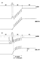
図2(a)及び(b)は、第1実施形態の窒化物半導体積層体の模式的なエネルギーバンド図である。図2(a)は熱平衡状態(バイアス電圧が0V)を、図2(b)は順バイアス状態を表す。また、図2(b)には、電子密度のエネルギー分布nと、ホール密度のエネルギー分布pもあわせて示している。 2A and 2B are schematic energy band diagrams of the nitride semiconductor multilayer body of the first embodiment. 2A shows a thermal equilibrium state (bias voltage is 0 V), and FIG. 2B shows a forward bias state. FIG. 2B also shows an electron density energy distribution n and a hole density energy distribution p.
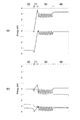
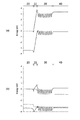
図9(a)及び(b)は、第1実施形態の窒化物半導体積層体のシミュレーションによるエネルギーバンド図である。図9(a)は熱平衡状態(バイアス電圧が0V)を、図9(b)は順バイアス状態を表す。また、図9(a)にはフェルミレベル、図9(b)には電子の擬フェルミレベルおよびホールの擬フェルミレベルを1点鎖線で示している。また、図10(a)、(b)は、それぞれ第1実施形態の窒化物半導体積層体のシミュレーションによる熱平衡状態でのキャリア分布、電界強度を表す。 FIGS. 9A and 9B are energy band diagrams obtained by simulation of the nitride semiconductor multilayer body of the first embodiment. FIG. 9A shows a thermal equilibrium state (bias voltage is 0 V), and FIG. 9B shows a forward bias state. Further, FIG. 9A shows a Fermi level, and FIG. 9B shows a pseudo Fermi level of electrons and a pseudo Fermi level of holes by a one-dot chain line. FIGS. 10A and 10B show carrier distribution and electric field strength in a thermal equilibrium state by simulation of the nitride semiconductor multilayer body of the first embodiment, respectively.
なお、本明細書において、窒化物半導体は、InxAlyGa1−x−yN(0≦x≦1、0≦y≦1、x+y≦1)で表される。なお、導電型を制御するために添加される不純物を含むものも窒化物半導体に含まれるものとする。 Note that in this specification, a nitride semiconductor is represented by In x Al y Ga 1-xy N (0 ≦ x ≦ 1, 0 ≦ y ≦ 1, x + y ≦ 1). Note that a nitride semiconductor includes an impurity added to control the conductivity type.
第1実施形態の窒化物半導体積層体(以下、単に積層体ともいう)は、n型クラッド層20と、p型クラッド層40と、n型クラッド層20とp型クラッド層40との間に設けられた活性層30と、を有する。
The nitride semiconductor multilayer body of the first embodiment (hereinafter also simply referred to as a multilayer body) includes an n-
n型クラッド層20は、例えば、n型GaN層であり、所謂pn接合の順バイアス時に活性層30に電子を供給する。また、p型クラッド層40は、例えば、p型GaN層であり、所謂pn接合の順バイアス時に活性層30にホールを供給する。
The n-
活性層30は、複数の井戸層31と複数の障壁層32が交互に積層された多重量子井戸(MQW:Multiple Quantum well)構造を有する。なお、井戸層31と障壁層32の積層数は、任意である。
The
井戸層31は、n型クラッド層20およびp側クラッド層40よりもバンドギャップエネルギーが小さい。障壁層32は、井戸層31を積層方向に挟んでおり、井戸層31よりもバンドギャップエネルギーが大きい。
The
井戸層31は、例えば、アンドープのInxGa1−xN(0<x<1)を含む。障壁層32は、例えば、アンドープのGaNを含み、Inを実質的に含まない。また、障壁層32がInを含む場合、障壁層32におけるIn組成比は、井戸層31におけるIn組成比よりも低い。活性層30から放出される光のピーク波長は、例えば400nm以上650nm以下である。
ここで、アンドープとは、結晶成長の際に不純物を意図的に入れていないことを表す。逆に、n型またはp型と記述している場合は意図的に導電型を制御する不純物をドープすることを指すものとする。
The
Here, undoped means that impurities are not intentionally added during crystal growth. On the other hand, the description of n-type or p-type refers to intentionally doping an impurity that controls the conductivity type.
さらに、第1実施形態の積層体は、活性層30から見てn型クラッド層20側に位置するようにn側電子バリア層21を有し、活性層30のn型クラッド層20側の端に近接する領域に電子バリア層を設けている。例えば、図1に示す例では、n側電子バリア層21は、活性層30の最もn型クラッド層20寄りの障壁層32と、n型クラッド層20との間に設けられている。あるいは、n側電子バリア層21は、n型クラッド層20中における活性層30側の領域に設けられていてもよい。
Furthermore, the stacked body of the first embodiment has an n-side
いずれにしても、n側電子バリア層21は、活性層30からn型クラッド層20側に向けて電子の拡散長範囲内の領域に設けられている。さらに、具体的には、n側電子バリア層21は、活性層30の最もn型クラッド層20寄りの井戸層31または障壁層32から、n型クラッド層20側に向けて電子拡散長範囲内の領域に設けられている。n側電子バリア層21は、n型クラッド層20から活性層30に注入される電子のうち、n側電子バリア層21のエネルギー障壁高さ以下のエネルギーの電子の注入を抑制する。
In any case, the n-side
n側電子バリア層21は、n型クラッド層20および障壁層32よりもバンドギャップエネルギーが大きく、例えば、アンドープのAlGaN層である。
The n-side
ここで、図15(a)及び(b)は、一般的に用いられている窒化物半導体積層体のエネルギーバンド図を参照例として示したものである。図15(a)は熱平衡状態(バイアス電圧が0V)のエネルギーバンド図を表し、図15(b)は順バイアス時のエネルギーバンド図を表す。また、図15(b)には、電子密度のエネルギー分布nと、ホール密度のエネルギー分布pもあわせて示している。 Here, FIGS. 15A and 15B show energy band diagrams of commonly used nitride semiconductor stacks as reference examples. FIG. 15A shows an energy band diagram in a thermal equilibrium state (bias voltage is 0 V), and FIG. 15B shows an energy band diagram in forward bias. FIG. 15B also shows an energy distribution n of electron density and an energy distribution p of hole density.
図13(a)及び(b)は、参照例の窒化物半導体積層体のシミュレーションによるエネルギーバンド図である。図13(a)は熱平衡状態(バイアス電圧が0V)を、図13(b)は順バイアス状態を表す。また、図13(a)にはフェルミレベル、図13(b)には電子の擬フェルミレベルおよびホールの擬フェルミレベルを1点鎖線で示している。 FIGS. 13A and 13B are energy band diagrams obtained by simulation of the nitride semiconductor multilayer body of the reference example. FIG. 13A shows a thermal equilibrium state (bias voltage is 0 V), and FIG. 13B shows a forward bias state. Further, FIG. 13A shows a Fermi level, and FIG. 13B shows an electron pseudo-Fermi level and a hole pseudo-Fermi level by a one-dot chain line.
参照例の積層体においては、前述した第1実施形態の積層体のn側電子バリア層21が設けられず、代わりに、p型クラッド層40と活性層30との間に、p側電子バリア層41が設けられている。図13の参照例の窒化物半導体積層体のシミュレーションによるエネルギーバンド図は、図9の層構成からn側電子バリア層21を除き、p側電子バリア層41を設けたものに相当し、上記以外の構成のパラメータは全て図9のシミュレーションと同一である。
In the laminated body of the reference example, the n-side
p側電子バリア層41は、p型クラッド層40および障壁層32よりもバンドギャップエネルギーが大きく、例えば、p型AlGaN層である。p側電子バリア層41は、活性層30からp型クラッド層40側への電子のオーバーフローを抑制する。
The p-side
InGaN/GaN系の多重量子井戸では、伝導帯のバリア高さ(ヘテロ界面のエネルギー不連続量)と価電子帯のバリア高さがほぼ同等にもかかわらず、電子の有効質量に比べてホールの有効質量が数倍大きいため(例えばGaNの場合、電子の有効質量0.2に対してホールの有効質量が1.7など)、pn接合の順バイアス時に、電子とホールで量子井戸の障壁層32を乗り越えられる量に大幅な差が生じ、活性層30(多重量子井戸)のn型クラッド層側の量子井戸までホールが注入され難いという問題がある。 In InGaN / GaN multiple quantum wells, the barrier height of the conduction band (the energy discontinuity at the heterointerface) and the barrier height of the valence band are almost equal, but the hole mass is higher than the effective mass of electrons. Since the effective mass is several times larger (for example, in the case of GaN, the effective mass of holes is 1.7 relative to the effective mass of electrons of 0.2), the barrier layer of the quantum well is composed of electrons and holes when the pn junction is forward biased. There is a significant difference in the amount that can be surpassed by 32, and there is a problem that holes are difficult to be injected up to the quantum well on the n-type cladding layer side of the active layer 30 (multiple quantum well).
すなわち、p型クラッド層40から注入されるホールが活性層30のp型クラッド層40側に偏在してしまい、活性層30のn型クラッド層20側でホールが不足し、活性層30内のキャリア注入が不均一になって発光効率の低下をまねく。このことは、図13(b)の参照例のホール擬フェルミレベルが、n型クラッド層20側で低下する(ホールが減少してバンドギャップの中央寄りになる)ことからも確認できる。この場合、n型クラッド層20側に近い量子井戸では殆どホールが存在しないホール枯渇状態になっている。また、キャリア注入の不十分な量子井戸31は、光利得(キャリア再結合による光放出)が低いため、他の量子井戸が発する光を吸収してキャリア(電子およびホール)生成する光吸収体として機能し、光吸収により生成したキャリアが一切の損失無く再結合しない限り、全体としてのキャリア損失(発光効率低下)を生じてしまう。参照例の窒化物半導体積層体では、p型クラッド層40側の量子井戸にホールが集中する結果、電荷中性則を保つため電子がp型クラッド層40側に引き寄せられ、p側電子バリア層41でp型クラッド層40への電子拡散を抑え込まれるため、活性層30のp側電子バリア層41に接する障壁層32の部分に過剰に電子が集中し、障壁層32でのAuger効果(非発光キャリア再結合)を促進させるキャリア損失が生じやすくなる。本来、Auger効果はキャリア密度の3乗に比例する効果のため、電子の集中部を作らないよう構成する必要がある。また、p側電子バリア層41に接する障壁層32の部分に過剰に電子が集中する結果、p側電子バリア層41のバンド変形(価電子帯側への沈み込み)が起こってp側電子バリア層41の電子バリア効果が薄れ、結果として電子のオーバーフローを生じやすくなる。
That is, holes injected from the p-
これらの問題を鑑み、第1実施形態によれば、活性層30のn型クラッド層20側の端に近接する領域にn側電子バリア層21を設けている。n側電子バリア層21は、例えばGaN層であるn型クラッド層20よりもバンドギャップエネルギーが大きなAlGaN層であり、n型クラッド層20に対して電子のヘテロ障壁を有している。即ち、n側電子バリア層21は、n型クラッド層20中の電子にとって障壁となり、n型クラッド層20の電子のうちAlGaNとGaNの伝導帯ヘテロ障壁よりエネルギーの低い電子の活性層30への注入を抑制する。これはn型クラッド層20とp型クラッド層40の間にpn接合の順バイアスが印加されて電流が流れている場合においても同様である。
この結果、pn接合に順バイアスが印加された場合に、活性層30よりn型クラッド層20側(n型クラッド層20とn側電子バリア層21の界面近傍)に電子蓄積され、その電子蓄積量に相当するホールが、電荷中性則を保つためにp型クラッド層40から活性層30に注入されてn型クラッド層20側まで引き寄せられるようになる。このため、活性層30(多重量子井戸)のn型クラッド層20側の量子井戸にまでホールが供給されるようになり、活性層30内の注入キャリア分布が均等化されることで発光効率の向上が可能になる。
また、n側電子バリア層21とn型クラッド層20の電子親和力の差により、熱平衡状態において、n側電子バリア層21からn型クラッド層20に電子が移動してn側電子バリア層21が空乏化し、n側電子バリア層21とn型クラッド層20の界面に電子の高濃度領域が形成される。n側電子バリア層21とn型クラッド層20の電子障壁(伝導帯ヘテロ障壁)がある程度大きくなると、n型クラッド層20のn側電子バリア層21界面付近のバンド変形部に量子準位が形成され、n側電子バリア層21およびn型クラッド層20の電子を引き寄せて二次元電子ガスを形成するようになる。
In view of these problems, according to the first embodiment, the n-side
As a result, when a forward bias is applied to the pn junction, electrons are accumulated from the
Further, due to the difference in electron affinity between the n-side
このため、熱平衡状態において、n側電子バリア層21および活性層30の残留電子が電子高濃度領域または二次元電子ガスに吸収されて空乏化(電子が枯渇化)し易くなる。この電子親和力の効果でInxAlyGa1−x−yN(0≦x≦1、0≦y≦1、x+y≦1)窒化物半導体のピエゾ効果が増大、即ち、n側電子バリア層21がほぼ真性領域まで空乏化することでn側電子バリア層21のピエゾ効果が増大する(残留キャリアによる電界遮蔽効果が無くなる)ことにより、図9(a)に示すようにn側電子バリア層21の両端に大きな電位差を生じ、これにより、活性層30の電子を枯渇化(n型クラッド層20側に排出)させ、更に電子高濃度領域(または二次元電子ガス)の負電荷によりp型クラッド層40からホールを引き寄せて、活性層30およびn側電子バリア層21にp型不純物(例えばMg等)を一切、意図的にドープすることなく、即ち、アンドープの状態で活性層30を疑似的にp領域化させることができる。実際の結晶成長層ではp型クラッド層40などから熱拡散してくるMgが僅かに含まれる場合もあるが、上記の疑似p領域化は、そのような意図しない不純物も一切含まずに実質的なp領域化が可能ということを指している。この結果、n側電子バリア層21を疑似的なpn接合領域とし、pn接合の拡散電位をn側電子バリア層21部分に集中させ、pn接合の拡散電位による最大電界領域を活性層30の中央部よりn型クラッド層20側に位置させることが可能になる。ここでpn接合の拡散電位による最大電界領域とは、ヘテロ接合界面等でpn接合が無くても生じる局所的な電界を除き、pn接合の拡散電位で生じる電界の最大領域(エネルギーバンドの傾斜が最大となる部分)を指すものとする。
このようにして構成した場合のバンド構造を図9(a)に示す。図9(a)は、図2(a)の模式的なバンド構造(簡単化のため窒化物半導体のピエゾ電界効果を省略)とは異なり、各窒化物半導体のピエゾ効果も取り入れてシミュレーションした結果である。図9(a)及び図10(b)に示されるように、n側電子バリア層21の領域にpn接合の拡散電位による非常に大きな電界が集中しており、活性層30(量子井戸31および障壁層32の全て)が実質的なp領域になっていることが分る。勿論、上記のシミュレーションでは活性層30に一切のp型不純物を含ませておらず、p型クラッド層40などのp型不純物が拡散して活性層30に混入していない理想的な結晶成長層でのバンド構造をシミュレーションしている。また、シミュレーションでは実際の結晶成長層での残留キャリアを考慮し、1×1016cm−3の電子濃度を初期値として設定している。即ち、活性層30を1×1016cm−3のn型層として初期設定しているにもかかわらず、構造的な効果でp領域化していることになる。このことは、図10(a)に示すように、熱平衡状態でも活性層30がホールで満たされていることからもわかる。この疑似p領域化の効果により、図13(a)に示す参照例に比べて、活性層30におけるpn接合の拡散電位による電界が大幅に緩和されていることも一目瞭然である。
For this reason, in the thermal equilibrium state, residual electrons in the n-side
FIG. 9A shows a band structure in such a configuration. FIG. 9A differs from the schematic band structure of FIG. 2A (the piezo electric field effect of the nitride semiconductor is omitted for the sake of simplification), and the simulation results include the piezo effect of each nitride semiconductor. It is. As shown in FIGS. 9A and 10B, a very large electric field due to the diffusion potential of the pn junction is concentrated in the region of the n-side
このようにpn接合による最大電界領域を活性層30よりn型クラッド層20側に位置させるための構成例としては、例えば、n型クラッド層20をGaN(例えばキャリア濃度を1×1019cm−3)、n側電子バリア層21をAl0.25Ga0.75N(例えばアンドープ)で厚さ15nmとし、活性層30(障壁層GaN、井戸層InGaN)は全てアンドープとする。図9(a)はこの条件でのシミュレーション結果であり、活性層30を疑似的にp領域化するための条件として、n型クラッド層20がGaN(例えばキャリア濃度を1×1019cm−3)、活性層30(障壁層GaN、井戸層InGaN)が全てアンドープの場合、n側電子バリア層21のAl組成が0.05以上、厚さが2nm以上が望ましい。
As a configuration example for positioning the maximum electric field region by the pn junction on the n-
図17(a)は第5実施形態の窒化物半導体積層体の模式断面図であり、図17(b)は第5実施形態の窒化物半導体積層体の模式的なエネルギーバンド図である。 FIG. 17A is a schematic cross-sectional view of the nitride semiconductor multilayer body of the fifth embodiment, and FIG. 17B is a schematic energy band diagram of the nitride semiconductor multilayer body of the fifth embodiment.
n側電子バリア層は、AlGaN層の単層に限らない。図17(a)及び(b)に示す実施形態によれば、結晶成長層の応力制御のために、n側電子バリア層は、複数のアンドープAlGaN層21と、複数のアンドープGaN層25を含んでいる。 The n-side electron barrier layer is not limited to a single AlGaN layer. According to the embodiment shown in FIGS. 17A and 17B, the n-side electron barrier layer includes a plurality of undoped AlGaN layers 21 and a plurality of undoped GaN layers 25 for stress control of the crystal growth layer. It is out.
n側電子バリア層は、例えば、3層のAl0.25Ga0.75N層21を含んでいる。それぞれのAl0.25Ga0.75N層21の厚さは、例えば5nmである。AlGaN層21の間にGaN層25が設けられている。それぞれのGaN層25の厚さは、例えば5nmである。
The n-side electron barrier layer includes, for example, three Al 0.25 Ga 0.75 N layers 21. The thickness of each Al 0.25 Ga 0.75 N layer 21 is, for example, 5 nm. A
上記したバンド構造とするためには、活性層30、n側電子バリア層21のアンドープ時の残留キャリア密度(電子密度)は、例えば、1×1016cm−3以下が望ましい。
In order to obtain the above band structure, the residual carrier density (electron density) when the
n側電子バリア層21を設けることにより、熱平衡状態で、pn接合の空乏層は、n側電子バリア層21により電子が蓄積して高キャリア密度化しているn側よりもp側に伸び易くなる。そして、図9(b)に示すように、順バイアス時には、n型クラッド層20とn側電子バリア層21との界面の蓄積電子電荷(n++)を電荷中性化するためにホールが引き寄せられ、活性層30のn型クラッド層20側の領域(量子井戸)までホールが注入されやすくなる。熱平衡時にp側に非対称的に伸びていた空乏層は、順バイアス時、p側から縮小し、活性層30へのホール注入が促進されることになる。
By providing the n-side
この結果、活性層30に対する電子とホールの注入が均一化されて発光効率が高まり、また、活性層内で電子が局所的に集中する部分が無くなってAuger効果が激減し、高注入時のドループ現象を緩和することができる。
As a result, the injection of electrons and holes into the
図14は、GaN層とGaN層との間に挟まれたAlGaN層の厚さ(nm)と、電子トンネル確率(%)との関係を表すグラフである。伝導帯の底からのAlGaN層の障壁エネルギーΔEcは350meV、GaN領域の電子の有効質量meは0.22としている。 FIG. 14 is a graph showing the relationship between the thickness (nm) of the AlGaN layer sandwiched between the GaN layer and the GaN layer and the electron tunnel probability (%). Barrier energy ΔEc of AlGaN layer from the bottom of the conduction band is 350 meV, the effective mass m e of electrons GaN region is 0.22.
また、グラフ中、a、b、c、d、e、f、g、h、iは、それぞれ、ΔEc比での電子エネルギー0.1、0.2、0.3、0.4、0.5、0.6、0.7、0.8、0.9を表す。 In the graph, a, b, c, d, e, f, g, h, and i are electron energies 0.1, 0.2, 0.3, 0.4, 0,. It represents 5, 0.6, 0.7, 0.8, 0.9.
n側電子バリア層21として機能するAlGaN層があまりに薄いとトンネル効果により電子に対して障壁にならない。そこで、図14の結果によれば、n側電子バリア層21としてのAlGaN層の厚さは2nm以上が望ましいことが分る。
If the AlGaN layer functioning as the n-side
また、n側電子バリア層21が厚すぎると、n型クラッド層20とn側電子バリア層21との界面の蓄積電子が活性層30から遠くなり、蓄積電子電荷によるホールの引き込み効果が不十分になる。
If the n-side
したがって、n側電子バリア層21の厚さは、2nm以上50nm以下が望ましく、理想的には2nm以上5nm以下が望ましい。
また、n側電子バリア層21の位置は、活性層30へ電子注入を行うため、活性層30から電子拡散長以下の範囲とすることが望ましい。
Therefore, the thickness of the n-side
Further, the position of the n-side
また、n型クラッド層20とn側電子バリア層21との間の障壁を急峻にするために、n型クラッド層20とn側電子バリア層21との間の遷移層の厚さは2nm以下が望ましい。
Further, in order to make the barrier between the n-
また、AlGaN層中の酸素は自由電子を供給するドナーとして機能する。したがって、n側電子バリア層21としてAlGaN層を使い、n側電子バリア層21において局所的に酸素濃度を高くすることで、n型クラッド層(GaN層)20との界面の蓄積電子を増大させ、且つn側電子バリア層21のキャリア枯渇化を効果的に行わせ、前述したホール引き込み効果を高めることができる。
Further, oxygen in the AlGaN layer functions as a donor for supplying free electrons. Therefore, by using an AlGaN layer as the n-side
次に、図3は、第2実施形態の窒化物半導体積層体の模式断面図である。 Next, FIG. 3 is a schematic cross-sectional view of the nitride semiconductor multilayer body according to the second embodiment.
図4(a)及び(b)は、第2実施形態の窒化物半導体積層体の模式的なエネルギーバンド図である。図4(a)は熱平衡状態(バイアス電圧が0V)を、図4(b)は順バイアス状態を表す。また、図4(b)には、電子密度のエネルギー分布nと、ホール密度のエネルギー分布pもあわせて示している。 FIGS. 4A and 4B are schematic energy band diagrams of the nitride semiconductor multilayer body according to the second embodiment. 4A shows a thermal equilibrium state (bias voltage is 0 V), and FIG. 4B shows a forward bias state. FIG. 4B also shows an electron density energy distribution n and a hole density energy distribution p.
図11(a)及び(b)は、第2実施形態の窒化物半導体積層体のシミュレーションによるエネルギーバンド図である。図11(a)は熱平衡状態(バイアス電圧が0V)を、図11(b)は順バイアス状態を表す。また、図11(a)にはフェルミレベル、図11(b)には電子の擬フェルミレベルおよびホールの擬フェルミレベルを1点鎖線で示している。 FIGS. 11A and 11B are energy band diagrams obtained by simulation of the nitride semiconductor multilayer body of the second embodiment. FIG. 11A shows a thermal equilibrium state (bias voltage is 0 V), and FIG. 11B shows a forward bias state. Further, FIG. 11A shows the Fermi level, and FIG. 11B shows the pseudo-Fermi level of electrons and the pseudo-Fermi level of holes by a one-dot chain line.
第2実施形態においては、n側電子バリア層22として、n型クラッド層20および障壁層32よりもバンドギャップエネルギーが大きいn型AlGaN層が設けられている。その他構成および効果は、第1実施形態と同じである。
In the second embodiment, an n-type AlGaN layer having a larger band gap energy than the n-
n側電子バリア層22には、成膜時にn型不純物として例えばSiがドープされる。しかしながら、n側電子バリア層22中のキャリア(電子)は、n側電子バリア層22よりもエネルギーの低いn型クラッド層20および活性層30に拡散し、熱平衡状態において、n側電子バリア層22は空乏化(キャリアが枯渇化)し、二次元電子ガスを含む高濃度電子蓄積の効果およびピエゾ効果により、図11(a)のシミュレーション結果に示されるように、n側電子バリア層22の領域に非常に大きな電界が生じる。また、図13(a)に示す参照例に比べて、活性層30の電界は緩和される。
The n-side
上記したバンド構造とするためには、活性層30、空乏化(キャリアが枯渇化)したn側電子バリア層22のアンドープ時の残留キャリア密度(電子密度)は、例えば、1×1016cm−3以下が望ましい。
In order to obtain the above band structure, the residual carrier density (electron density) of the
そして、第2実施形態においても、順バイアス時には、n型クラッド層20とn側電子バリア層22との界面の蓄積電子電荷(n++)に対する電荷中性則でホールが引き寄せられ、活性層30のn型クラッド層20側の領域までホールが注入されやすくなる。この結果、活性層30に対する電子とホールの注入が均一化されて発光効率が高まり、また、活性層内で電子が局所的に集中する部分が無くなってAuger効果が激減し、高注入時のドループ現象を緩和できる。
Also in the second embodiment, at the time of forward bias, holes are attracted by the charge neutrality law with respect to the accumulated electron charge (n ++ ) at the interface between the n-
また、第1実施形態と同様、n側電子バリア層22の厚さは、2nm以上50nm以下が望ましく、理想的には2nm以上5nm以下が望ましい。また、n型クラッド層20とn側電子バリア層22との間の遷移層の厚さは2nm以下が望ましい。
As in the first embodiment, the thickness of the n-side
また、第2実施形態においても、n側電子バリア層21としてAlGaN層を使い、n側電子バリア層21において局所的に酸素濃度を高くすることで、n型クラッド層(GaN層)20との界面の蓄積電子を増大させ、且つn側電子バリア層21のキャリア枯渇化を効果的に行わせ、前述したホール引き込み効果を高めることができる。
Also in the second embodiment, an AlGaN layer is used as the n-side
次に、図5は、第3実施形態の窒化物半導体積層体の模式断面図である。 Next, FIG. 5 is a schematic cross-sectional view of the nitride semiconductor multilayer body of the third embodiment.
図6(a)及び(b)は、第3実施形態の窒化物半導体積層体の模式的なエネルギーバンド図である。図6(a)は熱平衡状態(バイアス電圧が0V)を、図6(b)は順バイアス状態を表す。また、図6(b)には、電子密度のエネルギー分布nと、ホール密度のエネルギー分布pもあわせて示している。 FIGS. 6A and 6B are schematic energy band diagrams of the nitride semiconductor multilayer body of the third embodiment. 6A shows a thermal equilibrium state (bias voltage is 0 V), and FIG. 6B shows a forward bias state. FIG. 6B also shows the energy distribution n of electron density and the energy distribution p of hole density.
第3実施形態においては、n側電子バリア層23として、n型クラッド層20および障壁層32よりもバンドギャップエネルギーが大きいp型AlGaN層をn型クラッド層20の内側に設けている。
In the third embodiment, a p-type AlGaN layer having a larger band gap energy than the n-
n側電子バリア層23には、成膜時にp型不純物として例えばMg、Zn、Cd、Cがドープされる。
The n-side
そして、第3実施形態においては、n側電子バリア層23(p型)がn型クラッド層20に挟まれて価電子帯レベルが揃えられるようにバンド構成されるため、順バイアス時にn型クラッド層20よりn側電子バリア層23が伝導帯側に突き出した形で低エネルギー電子のバリアとなり、n型クラッド層20とn側電子バリア層23との界面に電子を蓄積することができる。この界面の蓄積電子電荷(n++)に対する電荷中性則でホールが引き寄せられ、活性層30のn型クラッド層20側の領域までホールが注入されやすくなる。この結果、活性層30に対する電子とホールの注入が均一化されて発光効率が高まり、また、活性層内で電子が局所的に集中する部分が無くなってAuger効果が激減し、高注入時のドループ現象を緩和できる。
In the third embodiment, the n-side electron barrier layer 23 (p-type) is sandwiched between the n-type cladding layers 20 so that the valence band levels are uniform, so that the n-type cladding is forward biased. The n-side
また、第1実施形態と同様、n側電子バリア層23の厚さは、2nm以上50nm以下が望ましく、理想的には2nm以上5nm以下が望ましい。また、n型クラッド層20とn側電子バリア層23との間の遷移層の厚さは2nm以下が望ましい。
As in the first embodiment, the thickness of the n-side
また、AlGaNをp型にする不純物としてMgをドープした場合、MgはHと結びつきやすい。したがって、いずれもp型不純物(Mg)を含まないn型クラッド層(GaN)20および活性層(InGaN/GaN)30よりも、p型AlGaN層であるn側電子バリア層23において局所的に水素濃度が高くなっている。これは、n側電子バリア層23の欠陥の低減に寄与する。
尚、n側電子バリア層23は、第一の実施形態、第二の実施形態と同様にn型クラッド層20を挟まずに活性層30に接する構成とすることでも構わない。この場合、n側電子バリア層23(pドープ)により活性層30が持上げられて疑似p領域化しやすくなるという効果がある。
Further, when Mg is doped as an impurity that makes AlGaN p-type, Mg is likely to be combined with H. Accordingly, hydrogen is locally present in the n-side
Note that the n-side
次に、図7は、第4実施形態の窒化物半導体積層体の模式断面図である。 Next, FIG. 7 is a schematic cross-sectional view of the nitride semiconductor multilayer body of the fourth embodiment.
図8(a)及び(b)は、第4実施形態の窒化物半導体積層体の模式的なエネルギーバンド図である。図8(a)は熱平衡状態(バイアス電圧が0V)を、図8(b)は順バイアス状態を表す。また、図8(b)には、電子密度のエネルギー分布nと、ホール密度のエネルギー分布pもあわせて示している。 FIGS. 8A and 8B are schematic energy band diagrams of the nitride semiconductor multilayer body of the fourth embodiment. FIG. 8A shows a thermal equilibrium state (bias voltage is 0 V), and FIG. 8B shows a forward bias state. FIG. 8B also shows an energy distribution n of electron density and an energy distribution p of hole density.
図12(a)及び(b)は、第4実施形態の窒化物半導体積層体のシミュレーションによるエネルギーバンド図である。図12(a)は熱平衡状態(バイアス電圧が0V)を、図12(b)は順バイアス状態を表す。また、図12(a)にはフェルミレベル、図12(b)には電子の擬フェルミレベルおよびホールの擬フェルミレベルを1点鎖線で示している。 FIGS. 12A and 12B are energy band diagrams obtained by simulation of the nitride semiconductor multilayer body according to the fourth embodiment. 12A shows a thermal equilibrium state (bias voltage is 0 V), and FIG. 12B shows a forward bias state. FIG. 12A shows a Fermi level, and FIG. 12B shows an electron pseudo-Fermi level and a hole pseudo-Fermi level by a one-dot chain line.
第4実施形態においては、第1実施形態の構成に加えて、p側電子バリア層41をさらに備えている。
In the fourth embodiment, a p-side
p側電子バリア層41は、活性層30のp型クラッド層40側の端に近接する領域に設けられている。例えば、図7に示す例では、p側電子バリア層41は、活性層30の最もp型クラッド層40寄りの障壁層32と、p型クラッド層40との間に設けられている。
The p-side
p側電子バリア層41は、p型クラッド層40および障壁層32よりもバンドギャップエネルギーが大きく、例えば、p型AlGaN層である。
The p-side
p側電子バリア層41は、第1実施形態において僅かながらも活性層30からp型クラッド層40側へ漏れていく電子のオーバーフローを抑制する。このことは、図12(b)の電子の擬フェルミレベルが、p側電子バリア層41より先で低下する(電子が減少して中央寄りになる)ことからも確認できる。
The p-side
第4実施形態によれば、n型クラッド層20側およびp側クラッド層40の両方に電子バリア層を設けることで、活性層30での電子とホールの発光再結合効率をより高めることができる。
According to the fourth embodiment, by providing the electron barrier layer on both the n-
なお、第2実施形態および第3実施形態の構成においても、p型クラッド層40側にp側電子バリア層41をさらに設けてもよい。
In the configurations of the second and third embodiments, a p-side
図16は、実施形態の半導体発光素子の模式断面図である。図16には、半導体発光素子の一例として、LED(Light Emitting Diode)を示す。 FIG. 16 is a schematic cross-sectional view of the semiconductor light emitting device of the embodiment. FIG. 16 shows an LED (Light Emitting Diode) as an example of a semiconductor light emitting element.
実施形態の半導体発光素子は、窒化物半導体層10を有する。窒化物半導体層10は、前述したいずれかの実施形態の窒化物半導体積層体を含む。
The semiconductor light emitting device of the embodiment has a
窒化物半導体層10は、基板1上に、有機金属気相成長(MOCVD:metal organic chemical vapor deposition)法によって形成される。あるいは、分子線エピタキシー()MBE:molecular beam epitaxy)法によって窒化物半導体層10を基板1上に形成してもよい。
The
基板1は、例えば、シリコン基板、サファイア基板、SiC基板、GaN基板などを用いることができる。
As the
また、窒化物半導体層10は、前述した層(n型クラッド層、活性層、p型クラッド層、n側電子バリア層、p側電子バリア層)以外に、基板1と窒化物半導体との格子定数の不一致を緩和するバッファ層、電極とのコンタクト層などを含むことができる。また、n型クラッド層と基板1との間に、SLS(strained layer super lattice)バッファ層を形成して格子欠陥の低減化を図ることでもよい。
The
窒化物半導体層10は、基板1の反対側に、p型層の面10pと、n型層の面10nとを有する。n型層の面10n上にはn側電極パッド2が設けられている。p型層の面10p上にはp側電極3(例えばITO(Indium Tin Oxide)などの透明電極やAg電極)が設けられ、そのp側電極3上にはp側電極パッド4が設けられている。基板1はそのまま残すことでも、除去することでも構わない。前者の場合には、p側電極3を透明電極とすることが望ましく、後者の場合には、p側電極3をAgとして基板を除去した面から光を取り出すことでも構わない。また、後者の場合、n側電極を基板を除去した面に設けることでも構わなく、n側電極として透明電極を形成してn電極パッド2を部分的に設ける構成としてもよい。
The
前述した実施形態の窒化物半導体積層体を含む発光素子(LED)は、高い発光効率を有する。 The light emitting element (LED) including the nitride semiconductor multilayer body of the embodiment described above has high light emission efficiency.
なお、実施形態の窒化物半導体積層体は、LEDに限らず、LD(Laser Diode)にも適用可能である。 In addition, the nitride semiconductor laminated body of embodiment is applicable not only to LED but LD (Laser Diode).
本発明のいくつかの実施形態を説明したが、これらの実施形態は、例として提示したものであり、発明の範囲を限定することは意図していない。例えば、前述したn側電子バリア層21〜23およびはp側電子バリア層41は複数層設けられても構わず、また、その複数の電子バリア層の組成が異なっていても構わない。これら新規な実施形態は、その他の様々な形態で実施されることが可能であり、発明の要旨を逸脱しない範囲で、種々の省略、置き換え、変更を行うことができる。これら実施形態やその変形は、発明の範囲や要旨に含まれるとともに、特許請求の範囲に記載された発明とその均等の範囲に含まれる。
Although several embodiments of the present invention have been described, these embodiments are presented by way of example and are not intended to limit the scope of the invention. For example, a plurality of the n-side electron barrier layers 21 to 23 and the p-side
1…基板、2…n側電極パッド、3…透明電極、4…p側電極パッド、10…窒化物半導体積層体、20…n型クラッド層、21,22,23…n側電子バリア層、30…活性層、31…井戸層、32…障壁層、40…p型クラッド層、41…p側電子バリア層
DESCRIPTION OF
Claims (14)
窒化物半導体を含むp型クラッド層と、
前記n型クラッド層と前記p型クラッド層との間に設けられ窒化物半導体を含む活性層であって、複数の井戸層と、それぞれの前記井戸層を挟み前記井戸層よりもバンドギャップエネルギーが大きい複数の障壁層と、を有する活性層と、
前記活性層の前記n型クラッド層側の端に近接する領域であって、前記活性層から電子拡散長範囲内の領域に設けられ、前記活性層へ所定エネルギー以下の電子注入を抑制するn側電子バリア層と、
を備えた窒化物半導体積層体。 An n-type cladding layer containing a nitride semiconductor;
A p-type cladding layer including a nitride semiconductor;
An active layer that is provided between the n-type cladding layer and the p-type cladding layer and includes a nitride semiconductor, and has a plurality of well layers and a band gap energy between the well layers and the well layers. An active layer having a plurality of large barrier layers;
An n-side which is provided in a region close to the end of the active layer on the n-type cladding layer side and within an electron diffusion length range from the active layer, and suppresses electron injection of a predetermined energy or less into the active layer An electronic barrier layer;
A nitride semiconductor laminate comprising:
窒化物半導体を含むp型クラッド層と、
前記n型クラッド層と前記p型クラッド層との間に設けられ窒化物半導体を含む活性層であって、複数の井戸層と、それぞれの前記井戸層を挟み前記井戸層よりもバンドギャップエネルギーが大きい複数の障壁層と、を有する活性層と、
前記活性層の前記n型クラッド層側の端に近接する領域であって、前記活性層から電子拡散長範囲内の領域に設けられ、前記n型クラッド層および前記障壁層よりもバンドギャップエネルギーが大きい窒化物半導体を含むn側電子バリア層と、
を備えた窒化物半導体積層体。 An n-type cladding layer containing a nitride semiconductor;
A p-type cladding layer including a nitride semiconductor;
An active layer that is provided between the n-type cladding layer and the p-type cladding layer and includes a nitride semiconductor, and has a plurality of well layers and a band gap energy between the well layers and the well layers. An active layer having a plurality of large barrier layers;
A region close to the end of the active layer on the n-type cladding layer side, provided in a region within the electron diffusion length range from the active layer, and has a band gap energy higher than that of the n-type cladding layer and the barrier layer. An n-side electron barrier layer comprising a large nitride semiconductor;
A nitride semiconductor laminate comprising:
窒化物半導体を含むp型クラッド層と、
前記n型クラッド層と前記p型クラッド層との間に設けられ窒化物半導体を含む活性層であって、複数の井戸層と、それぞれの前記井戸層を挟み前記井戸層よりもバンドギャップエネルギーが大きい複数の障壁層と、を有する活性層と、
前記活性層の前記n型クラッド層側の端に近接する領域に設けられ、前記n型クラッド層および前記障壁層よりもバンドギャップエネルギーが大きい窒化物半導体を含み、熱平衡状態で空乏化しているn側電子バリア層と、
を備えた窒化物半導体積層体。 An n-type cladding layer containing a nitride semiconductor;
A p-type cladding layer including a nitride semiconductor;
An active layer that is provided between the n-type cladding layer and the p-type cladding layer and includes a nitride semiconductor, and has a plurality of well layers and a band gap energy between the well layers and the well layers. An active layer having a plurality of large barrier layers;
N which is provided in a region adjacent to the end of the active layer on the n-type cladding layer side, includes a nitride semiconductor having a band gap energy larger than that of the n-type cladding layer and the barrier layer, and is depleted in a thermal equilibrium state A side electron barrier layer;
A nitride semiconductor laminate comprising:
窒化物半導体を含むp型クラッド層と、
前記n型クラッド層と前記p型クラッド層との間に設けられ窒化物半導体を含む活性層であって、複数の井戸層と、それぞれの前記井戸層を挟み前記井戸層よりもバンドギャップエネルギーが大きい複数の障壁層と、を有する活性層と、
前記活性層の前記n型クラッド層側の端に近接する領域に設けられ、前記n型クラッド層および前記障壁層よりもバンドギャップエネルギーが大きいAlGaNを含み、前記n型クラッド層および前記活性層よりも酸素濃度が高いn側電子バリア層と、
を備えた窒化物半導体積層体。 An n-type cladding layer containing a nitride semiconductor;
A p-type cladding layer including a nitride semiconductor;
An active layer that is provided between the n-type cladding layer and the p-type cladding layer and includes a nitride semiconductor, and has a plurality of well layers and a band gap energy between the well layers and the well layers. An active layer having a plurality of large barrier layers;
Provided in a region close to the end of the active layer on the n-type cladding layer side, including AlGaN having a band gap energy larger than that of the n-type cladding layer and the barrier layer, and from the n-type cladding layer and the active layer N-side electron barrier layer having a high oxygen concentration,
A nitride semiconductor laminate comprising:
p型GaNを含むp型クラッド層と、
前記n型クラッド層と前記p型クラッド層との間に設けられた活性層であって、アンドープInGaNを含む複数の井戸層と、それぞれの前記井戸層を挟み前記井戸層よりもバンドギャップエネルギーが大きくアンドープGaNを含む複数の障壁層と、を有する活性層と、
前記活性層の前記n型クラッド層側の端に近接する領域に設けられ、前記n型クラッド層および前記障壁層よりもバンドギャップエネルギーが大きくAlGaNを含むn側電子バリア層と、
を備え、
前記n型クラッド層における前記n側電子バリア層との界面付近に高濃度電子領域を有している窒化物半導体積層体。 an n-type cladding layer containing n-type GaN;
a p-type cladding layer containing p-type GaN;
An active layer provided between the n-type cladding layer and the p-type cladding layer, and having a plurality of well layers containing undoped InGaN and a band gap energy between the well layers sandwiching each well layer. A plurality of barrier layers comprising a large undoped GaN, and an active layer,
An n-side electron barrier layer that is provided in a region near the end of the active layer on the n-type cladding layer side and has a larger band gap energy than the n-type cladding layer and the barrier layer, and includes AlGaN;
With
A nitride semiconductor multilayer body having a high-concentration electron region in the vicinity of an interface between the n-type cladding layer and the n-side electron barrier layer.
前記n型クラッド層に接続されたn側電極と、
前記p型クラッド層に接続されたp側電極と、
を備えた半導体発光素子。 The nitride semiconductor multilayer body according to any one of claims 1 to 13,
An n-side electrode connected to the n-type cladding layer;
A p-side electrode connected to the p-type cladding layer;
A semiconductor light emitting device comprising:
Priority Applications (5)
| Application Number | Priority Date | Filing Date | Title |
|---|---|---|---|
| JP2014148507A JP2015188048A (en) | 2014-03-10 | 2014-07-22 | Nitride semiconductor laminate and semiconductor light-emitting element |
| US14/446,437 US20150255670A1 (en) | 2014-03-10 | 2014-07-30 | Nitride semiconductor stacked body and semiconductor light emitting device |
| EP14180012.8A EP2919282B1 (en) | 2014-03-10 | 2014-08-06 | Nitride semiconductor stacked body and semiconductor light emitting device comprising the same |
| TW103127611A TWI559567B (en) | 2014-03-10 | 2014-08-12 | Nitride semiconductor laminate and semiconductor light emitting device |
| HK16100123.2A HK1212507A1 (en) | 2014-03-10 | 2016-01-07 | Nitride semiconductor stacked body and semiconductor light emitting device |
Applications Claiming Priority (3)
| Application Number | Priority Date | Filing Date | Title |
|---|---|---|---|
| JP2014045977 | 2014-03-10 | ||
| JP2014045977 | 2014-03-10 | ||
| JP2014148507A JP2015188048A (en) | 2014-03-10 | 2014-07-22 | Nitride semiconductor laminate and semiconductor light-emitting element |
Publications (1)
| Publication Number | Publication Date |
|---|---|
| JP2015188048A true JP2015188048A (en) | 2015-10-29 |
Family
ID=51265617
Family Applications (1)
| Application Number | Title | Priority Date | Filing Date |
|---|---|---|---|
| JP2014148507A Abandoned JP2015188048A (en) | 2014-03-10 | 2014-07-22 | Nitride semiconductor laminate and semiconductor light-emitting element |
Country Status (5)
| Country | Link |
|---|---|
| US (1) | US20150255670A1 (en) |
| EP (1) | EP2919282B1 (en) |
| JP (1) | JP2015188048A (en) |
| HK (1) | HK1212507A1 (en) |
| TW (1) | TWI559567B (en) |
Cited By (2)
| Publication number | Priority date | Publication date | Assignee | Title |
|---|---|---|---|---|
| JP2018163941A (en) * | 2017-03-24 | 2018-10-18 | 日機装株式会社 | Semiconductor light-emitting element and manufacturing method of the same |
| JP2020074464A (en) * | 2017-03-24 | 2020-05-14 | 日機装株式会社 | Semiconductor light-emitting element and manufacturing method of the same |
Families Citing this family (4)
| Publication number | Priority date | Publication date | Assignee | Title |
|---|---|---|---|---|
| US9425351B2 (en) * | 2014-10-06 | 2016-08-23 | Wisconsin Alumni Research Foundation | Hybrid heterostructure light emitting devices |
| WO2017195502A1 (en) * | 2016-05-13 | 2017-11-16 | パナソニックIpマネジメント株式会社 | Nitride-based light emitting element |
| CN110447113B (en) | 2017-03-24 | 2022-08-12 | 威斯康星州男校友研究基金会 | III-V nitride based light-emitting devices with multilayer p-type contacts |
| US10217897B1 (en) | 2017-10-06 | 2019-02-26 | Wisconsin Alumni Research Foundation | Aluminum nitride-aluminum oxide layers for enhancing the efficiency of group III-nitride light-emitting devices |
Family Cites Families (17)
| Publication number | Priority date | Publication date | Assignee | Title |
|---|---|---|---|---|
| KR100425341B1 (en) * | 2000-02-08 | 2004-03-31 | 삼성전기주식회사 | Nitride semiconductor light emitting device |
| SG115549A1 (en) * | 2002-07-08 | 2005-10-28 | Sumitomo Chemical Co | Epitaxial substrate for compound semiconductor light emitting device, method for producing the same and light emitting device |
| JP3857295B2 (en) * | 2004-11-10 | 2006-12-13 | 三菱電機株式会社 | Semiconductor light emitting device |
| US7326963B2 (en) * | 2004-12-06 | 2008-02-05 | Sensor Electronic Technology, Inc. | Nitride-based light emitting heterostructure |
| KR100714553B1 (en) * | 2005-12-06 | 2007-05-07 | 삼성전기주식회사 | Nitride semiconductor light emitting device |
| KR100753518B1 (en) * | 2006-05-23 | 2007-08-31 | 엘지전자 주식회사 | Nitride-based light emitting device |
| JP2008235790A (en) * | 2007-03-23 | 2008-10-02 | Mitsubishi Electric Corp | Manufacturing method of semiconductor light element |
| JP5191843B2 (en) * | 2008-09-09 | 2013-05-08 | 株式会社東芝 | Semiconductor light emitting device and wafer |
| JP2011146650A (en) * | 2010-01-18 | 2011-07-28 | Sumitomo Electric Ind Ltd | Gan-group semiconductor light-emitting element and method of manufacturing the same |
| JP5533744B2 (en) * | 2010-03-31 | 2014-06-25 | 豊田合成株式会社 | Group III nitride semiconductor light emitting device |
| EP2408028B1 (en) * | 2010-07-16 | 2015-04-08 | LG Innotek Co., Ltd. | Light emitting device |
| JP5443324B2 (en) * | 2010-11-26 | 2014-03-19 | 株式会社東芝 | Optical semiconductor device |
| US8648384B2 (en) * | 2011-07-25 | 2014-02-11 | Lg Innotek Co., Ltd. | Light emitting device |
| US9123851B2 (en) * | 2011-07-26 | 2015-09-01 | Nichia Corporation | Semiconductor light emitting element |
| US9070613B2 (en) * | 2011-09-07 | 2015-06-30 | Lg Innotek Co., Ltd. | Light emitting device |
| US8975616B2 (en) * | 2012-07-03 | 2015-03-10 | Liang Wang | Quantum efficiency of multiple quantum wells |
| US8890114B2 (en) * | 2012-10-16 | 2014-11-18 | Epistar Corporation | Light-emitting device |
-
2014
- 2014-07-22 JP JP2014148507A patent/JP2015188048A/en not_active Abandoned
- 2014-07-30 US US14/446,437 patent/US20150255670A1/en not_active Abandoned
- 2014-08-06 EP EP14180012.8A patent/EP2919282B1/en active Active
- 2014-08-12 TW TW103127611A patent/TWI559567B/en active
-
2016
- 2016-01-07 HK HK16100123.2A patent/HK1212507A1/en unknown
Cited By (2)
| Publication number | Priority date | Publication date | Assignee | Title |
|---|---|---|---|---|
| JP2018163941A (en) * | 2017-03-24 | 2018-10-18 | 日機装株式会社 | Semiconductor light-emitting element and manufacturing method of the same |
| JP2020074464A (en) * | 2017-03-24 | 2020-05-14 | 日機装株式会社 | Semiconductor light-emitting element and manufacturing method of the same |
Also Published As
| Publication number | Publication date |
|---|---|
| HK1212507A1 (en) | 2016-06-10 |
| TW201535777A (en) | 2015-09-16 |
| EP2919282B1 (en) | 2019-06-19 |
| TWI559567B (en) | 2016-11-21 |
| US20150255670A1 (en) | 2015-09-10 |
| EP2919282A1 (en) | 2015-09-16 |
Similar Documents
| Publication | Publication Date | Title |
|---|---|---|
| JP5284365B2 (en) | LED with current spreading layer | |
| TWI402998B (en) | Nitride semiconductor component | |
| CN105917476B (en) | Its active area includes the light emitting diode of InN layers | |
| JP4892618B2 (en) | Semiconductor light emitting device | |
| JP2015188048A (en) | Nitride semiconductor laminate and semiconductor light-emitting element | |
| CN103489973B (en) | Semiconductor light emitting structure | |
| US20120273753A1 (en) | Semiconductor light emitting device | |
| KR20130128931A (en) | N-algan thin film and light emitting device for emitting ultraviolet | |
| JP2010263085A (en) | Light emitting element | |
| JP5935178B2 (en) | Semiconductor light emitting device | |
| US20170062660A1 (en) | Nitride semiconductor stacked body and semiconductor light emitting device | |
| JP2013122950A (en) | Group iii nitride semiconductor light-emitting element | |
| JP4894398B2 (en) | Semiconductor laser device | |
| US20080175293A1 (en) | Semiconductor laser device | |
| KR20120022280A (en) | Nitride semiconductor light emitting device | |
| JP5948767B2 (en) | Nitride semiconductor light emitting device | |
| JP2014160739A (en) | Semiconductor light-emitting element and manufacturing method | |
| JP5337862B2 (en) | Semiconductor light emitting device | |
| WO2021172171A1 (en) | Laser element | |
| JP6218791B2 (en) | Nitride semiconductor laser device | |
| JP2013069795A (en) | Semiconductor light-emitting element | |
| JP6192722B2 (en) | Optoelectronic semiconductor body and optoelectronic semiconductor chip | |
| JP2022163904A (en) | Semiconductor light-emitting element | |
| CN107968138B (en) | A nitride light-emitting diode | |
| JP4786202B2 (en) | Semiconductor light emitting device |
Legal Events
| Date | Code | Title | Description |
|---|---|---|---|
| A621 | Written request for application examination |
Free format text: JAPANESE INTERMEDIATE CODE: A621 Effective date: 20160830 |
|
| A762 | Written abandonment of application |
Free format text: JAPANESE INTERMEDIATE CODE: A762 Effective date: 20170403 |
|
| A977 | Report on retrieval |
Free format text: JAPANESE INTERMEDIATE CODE: A971007 Effective date: 20170412 |