JP2014505367A - Method for integrating electronic components on printed circuit board or printed circuit board intermediate, and printed circuit board or printed circuit board intermediate - Google Patents
Method for integrating electronic components on printed circuit board or printed circuit board intermediate, and printed circuit board or printed circuit board intermediate Download PDFInfo
- Publication number
- JP2014505367A JP2014505367A JP2013550705A JP2013550705A JP2014505367A JP 2014505367 A JP2014505367 A JP 2014505367A JP 2013550705 A JP2013550705 A JP 2013550705A JP 2013550705 A JP2013550705 A JP 2013550705A JP 2014505367 A JP2014505367 A JP 2014505367A
- Authority
- JP
- Japan
- Prior art keywords
- printed circuit
- circuit board
- layer
- conductive layer
- electronic component
- Prior art date
- Legal status (The legal status is an assumption and is not a legal conclusion. Google has not performed a legal analysis and makes no representation as to the accuracy of the status listed.)
- Granted
Links
Images


Classifications
-
- H—ELECTRICITY
- H05—ELECTRIC TECHNIQUES NOT OTHERWISE PROVIDED FOR
- H05K—PRINTED CIRCUITS; CASINGS OR CONSTRUCTIONAL DETAILS OF ELECTRIC APPARATUS; MANUFACTURE OF ASSEMBLAGES OF ELECTRICAL COMPONENTS
- H05K1/00—Printed circuits
- H05K1/02—Details
- H05K1/0201—Thermal arrangements, e.g. for cooling, heating or preventing overheating
- H05K1/0203—Cooling of mounted components
- H05K1/0207—Cooling of mounted components using internal conductor planes parallel to the surface for thermal conduction, e.g. power planes
-
- H—ELECTRICITY
- H05—ELECTRIC TECHNIQUES NOT OTHERWISE PROVIDED FOR
- H05K—PRINTED CIRCUITS; CASINGS OR CONSTRUCTIONAL DETAILS OF ELECTRIC APPARATUS; MANUFACTURE OF ASSEMBLAGES OF ELECTRICAL COMPONENTS
- H05K1/00—Printed circuits
- H05K1/18—Printed circuits structurally associated with non-printed electric components
- H05K1/182—Printed circuits structurally associated with non-printed electric components associated with components mounted in the printed circuit board, e.g. insert mounted components [IMC]
- H05K1/185—Components encapsulated in the insulating substrate of the printed circuit or incorporated in internal layers of a multilayer circuit
- H05K1/188—Components encapsulated in the insulating substrate of the printed circuit or incorporated in internal layers of a multilayer circuit manufactured by mounting on or attaching to a structure having a conductive layer, e.g. a metal foil, such that the terminals of the component are connected to or adjacent to the conductive layer before embedding, and by using the conductive layer, which is patterned after embedding, at least partially for connecting the component
-
- B—PERFORMING OPERATIONS; TRANSPORTING
- B60—VEHICLES IN GENERAL
- B60T—VEHICLE BRAKE CONTROL SYSTEMS OR PARTS THEREOF; BRAKE CONTROL SYSTEMS OR PARTS THEREOF, IN GENERAL; ARRANGEMENT OF BRAKING ELEMENTS ON VEHICLES IN GENERAL; PORTABLE DEVICES FOR PREVENTING UNWANTED MOVEMENT OF VEHICLES; VEHICLE MODIFICATIONS TO FACILITATE COOLING OF BRAKES
- B60T5/00—Vehicle modifications to facilitate cooling of brakes
-
- B—PERFORMING OPERATIONS; TRANSPORTING
- B60—VEHICLES IN GENERAL
- B60T—VEHICLE BRAKE CONTROL SYSTEMS OR PARTS THEREOF; BRAKE CONTROL SYSTEMS OR PARTS THEREOF, IN GENERAL; ARRANGEMENT OF BRAKING ELEMENTS ON VEHICLES IN GENERAL; PORTABLE DEVICES FOR PREVENTING UNWANTED MOVEMENT OF VEHICLES; VEHICLE MODIFICATIONS TO FACILITATE COOLING OF BRAKES
- B60T17/00—Component parts, details, or accessories of power brake systems not covered by groups B60T8/00, B60T13/00 or B60T15/00, or presenting other characteristic features
- B60T17/18—Safety devices; Monitoring
- B60T17/22—Devices for monitoring or checking brake systems; Signal devices
-
- F—MECHANICAL ENGINEERING; LIGHTING; HEATING; WEAPONS; BLASTING
- F16—ENGINEERING ELEMENTS AND UNITS; GENERAL MEASURES FOR PRODUCING AND MAINTAINING EFFECTIVE FUNCTIONING OF MACHINES OR INSTALLATIONS; THERMAL INSULATION IN GENERAL
- F16D—COUPLINGS FOR TRANSMITTING ROTATION; CLUTCHES; BRAKES
- F16D13/00—Friction clutches
- F16D13/58—Details
- F16D13/72—Features relating to cooling
-
- F—MECHANICAL ENGINEERING; LIGHTING; HEATING; WEAPONS; BLASTING
- F16—ENGINEERING ELEMENTS AND UNITS; GENERAL MEASURES FOR PRODUCING AND MAINTAINING EFFECTIVE FUNCTIONING OF MACHINES OR INSTALLATIONS; THERMAL INSULATION IN GENERAL
- F16D—COUPLINGS FOR TRANSMITTING ROTATION; CLUTCHES; BRAKES
- F16D65/00—Parts or details
- F16D65/02—Braking members; Mounting thereof
- F16D65/12—Discs; Drums for disc brakes
- F16D65/128—Discs; Drums for disc brakes characterised by means for cooling
-
- F—MECHANICAL ENGINEERING; LIGHTING; HEATING; WEAPONS; BLASTING
- F16—ENGINEERING ELEMENTS AND UNITS; GENERAL MEASURES FOR PRODUCING AND MAINTAINING EFFECTIVE FUNCTIONING OF MACHINES OR INSTALLATIONS; THERMAL INSULATION IN GENERAL
- F16D—COUPLINGS FOR TRANSMITTING ROTATION; CLUTCHES; BRAKES
- F16D65/00—Parts or details
- F16D65/78—Features relating to cooling
- F16D65/80—Features relating to cooling for externally-engaging brakes
- F16D65/807—Features relating to cooling for externally-engaging brakes with open cooling system, e.g. cooled by air
-
- F—MECHANICAL ENGINEERING; LIGHTING; HEATING; WEAPONS; BLASTING
- F16—ENGINEERING ELEMENTS AND UNITS; GENERAL MEASURES FOR PRODUCING AND MAINTAINING EFFECTIVE FUNCTIONING OF MACHINES OR INSTALLATIONS; THERMAL INSULATION IN GENERAL
- F16D—COUPLINGS FOR TRANSMITTING ROTATION; CLUTCHES; BRAKES
- F16D65/00—Parts or details
- F16D65/78—Features relating to cooling
- F16D65/82—Features relating to cooling for internally-engaging brakes
- F16D65/827—Features relating to cooling for internally-engaging brakes with open cooling system, e.g. cooled by air
-
- F—MECHANICAL ENGINEERING; LIGHTING; HEATING; WEAPONS; BLASTING
- F16—ENGINEERING ELEMENTS AND UNITS; GENERAL MEASURES FOR PRODUCING AND MAINTAINING EFFECTIVE FUNCTIONING OF MACHINES OR INSTALLATIONS; THERMAL INSULATION IN GENERAL
- F16D—COUPLINGS FOR TRANSMITTING ROTATION; CLUTCHES; BRAKES
- F16D65/00—Parts or details
- F16D65/78—Features relating to cooling
- F16D65/84—Features relating to cooling for disc brakes
- F16D65/847—Features relating to cooling for disc brakes with open cooling system, e.g. cooled by air
-
- F—MECHANICAL ENGINEERING; LIGHTING; HEATING; WEAPONS; BLASTING
- F16—ENGINEERING ELEMENTS AND UNITS; GENERAL MEASURES FOR PRODUCING AND MAINTAINING EFFECTIVE FUNCTIONING OF MACHINES OR INSTALLATIONS; THERMAL INSULATION IN GENERAL
- F16D—COUPLINGS FOR TRANSMITTING ROTATION; CLUTCHES; BRAKES
- F16D69/00—Friction linings; Attachment thereof; Selection of coacting friction substances or surfaces
- F16D69/02—Composition of linings ; Methods of manufacturing
- F16D69/025—Compositions based on an organic binder
- F16D69/026—Compositions based on an organic binder containing fibres
-
- H—ELECTRICITY
- H05—ELECTRIC TECHNIQUES NOT OTHERWISE PROVIDED FOR
- H05K—PRINTED CIRCUITS; CASINGS OR CONSTRUCTIONAL DETAILS OF ELECTRIC APPARATUS; MANUFACTURE OF ASSEMBLAGES OF ELECTRICAL COMPONENTS
- H05K1/00—Printed circuits
- H05K1/02—Details
- H05K1/0201—Thermal arrangements, e.g. for cooling, heating or preventing overheating
- H05K1/0212—Printed circuits or mounted components having integral heating means
-
- H—ELECTRICITY
- H05—ELECTRIC TECHNIQUES NOT OTHERWISE PROVIDED FOR
- H05K—PRINTED CIRCUITS; CASINGS OR CONSTRUCTIONAL DETAILS OF ELECTRIC APPARATUS; MANUFACTURE OF ASSEMBLAGES OF ELECTRICAL COMPONENTS
- H05K1/00—Printed circuits
- H05K1/02—Details
- H05K1/0271—Arrangements for reducing stress or warp in rigid printed circuit boards, e.g. caused by loads, vibrations or differences in thermal expansion
-
- H—ELECTRICITY
- H05—ELECTRIC TECHNIQUES NOT OTHERWISE PROVIDED FOR
- H05K—PRINTED CIRCUITS; CASINGS OR CONSTRUCTIONAL DETAILS OF ELECTRIC APPARATUS; MANUFACTURE OF ASSEMBLAGES OF ELECTRICAL COMPONENTS
- H05K1/00—Printed circuits
- H05K1/02—Details
- H05K1/09—Use of materials for the conductive, e.g. metallic pattern
-
- H—ELECTRICITY
- H05—ELECTRIC TECHNIQUES NOT OTHERWISE PROVIDED FOR
- H05K—PRINTED CIRCUITS; CASINGS OR CONSTRUCTIONAL DETAILS OF ELECTRIC APPARATUS; MANUFACTURE OF ASSEMBLAGES OF ELECTRICAL COMPONENTS
- H05K1/00—Printed circuits
- H05K1/18—Printed circuits structurally associated with non-printed electric components
- H05K1/182—Printed circuits structurally associated with non-printed electric components associated with components mounted in the printed circuit board, e.g. insert mounted components [IMC]
- H05K1/185—Components encapsulated in the insulating substrate of the printed circuit or incorporated in internal layers of a multilayer circuit
- H05K1/186—Components encapsulated in the insulating substrate of the printed circuit or incorporated in internal layers of a multilayer circuit manufactured by mounting on or connecting to patterned circuits before or during embedding
- H05K1/187—Components encapsulated in the insulating substrate of the printed circuit or incorporated in internal layers of a multilayer circuit manufactured by mounting on or connecting to patterned circuits before or during embedding the patterned circuits being prefabricated circuits, which are not yet attached to a permanent insulating substrate, e.g. on a temporary carrier
-
- H—ELECTRICITY
- H05—ELECTRIC TECHNIQUES NOT OTHERWISE PROVIDED FOR
- H05K—PRINTED CIRCUITS; CASINGS OR CONSTRUCTIONAL DETAILS OF ELECTRIC APPARATUS; MANUFACTURE OF ASSEMBLAGES OF ELECTRICAL COMPONENTS
- H05K3/00—Apparatus or processes for manufacturing printed circuits
- H05K3/30—Assembling printed circuits with electric components, e.g. with resistor
-
- H10W70/093—
-
- H10W70/60—
-
- F—MECHANICAL ENGINEERING; LIGHTING; HEATING; WEAPONS; BLASTING
- F16—ENGINEERING ELEMENTS AND UNITS; GENERAL MEASURES FOR PRODUCING AND MAINTAINING EFFECTIVE FUNCTIONING OF MACHINES OR INSTALLATIONS; THERMAL INSULATION IN GENERAL
- F16D—COUPLINGS FOR TRANSMITTING ROTATION; CLUTCHES; BRAKES
- F16D65/00—Parts or details
- F16D65/78—Features relating to cooling
- F16D2065/783—Features relating to cooling cooling control or adjustment
-
- F—MECHANICAL ENGINEERING; LIGHTING; HEATING; WEAPONS; BLASTING
- F16—ENGINEERING ELEMENTS AND UNITS; GENERAL MEASURES FOR PRODUCING AND MAINTAINING EFFECTIVE FUNCTIONING OF MACHINES OR INSTALLATIONS; THERMAL INSULATION IN GENERAL
- F16D—COUPLINGS FOR TRANSMITTING ROTATION; CLUTCHES; BRAKES
- F16D66/00—Arrangements for monitoring working conditions, e.g. wear, temperature
- F16D2066/001—Temperature
-
- F—MECHANICAL ENGINEERING; LIGHTING; HEATING; WEAPONS; BLASTING
- F16—ENGINEERING ELEMENTS AND UNITS; GENERAL MEASURES FOR PRODUCING AND MAINTAINING EFFECTIVE FUNCTIONING OF MACHINES OR INSTALLATIONS; THERMAL INSULATION IN GENERAL
- F16D—COUPLINGS FOR TRANSMITTING ROTATION; CLUTCHES; BRAKES
- F16D69/00—Friction linings; Attachment thereof; Selection of coacting friction substances or surfaces
- F16D2069/004—Profiled friction surfaces, e.g. grooves, dimples
-
- F—MECHANICAL ENGINEERING; LIGHTING; HEATING; WEAPONS; BLASTING
- F16—ENGINEERING ELEMENTS AND UNITS; GENERAL MEASURES FOR PRODUCING AND MAINTAINING EFFECTIVE FUNCTIONING OF MACHINES OR INSTALLATIONS; THERMAL INSULATION IN GENERAL
- F16D—COUPLINGS FOR TRANSMITTING ROTATION; CLUTCHES; BRAKES
- F16D2200/00—Materials; Production methods therefor
- F16D2200/006—Materials; Production methods therefor containing fibres or particles
- F16D2200/0073—Materials; Production methods therefor containing fibres or particles having lubricating properties
-
- F—MECHANICAL ENGINEERING; LIGHTING; HEATING; WEAPONS; BLASTING
- F16—ENGINEERING ELEMENTS AND UNITS; GENERAL MEASURES FOR PRODUCING AND MAINTAINING EFFECTIVE FUNCTIONING OF MACHINES OR INSTALLATIONS; THERMAL INSULATION IN GENERAL
- F16D—COUPLINGS FOR TRANSMITTING ROTATION; CLUTCHES; BRAKES
- F16D2250/00—Manufacturing; Assembly
- F16D2250/0038—Surface treatment
- F16D2250/0046—Coating
-
- F—MECHANICAL ENGINEERING; LIGHTING; HEATING; WEAPONS; BLASTING
- F16—ENGINEERING ELEMENTS AND UNITS; GENERAL MEASURES FOR PRODUCING AND MAINTAINING EFFECTIVE FUNCTIONING OF MACHINES OR INSTALLATIONS; THERMAL INSULATION IN GENERAL
- F16D—COUPLINGS FOR TRANSMITTING ROTATION; CLUTCHES; BRAKES
- F16D2300/00—Special features for couplings or clutches
- F16D2300/10—Surface characteristics; Details related to material surfaces
-
- H—ELECTRICITY
- H05—ELECTRIC TECHNIQUES NOT OTHERWISE PROVIDED FOR
- H05K—PRINTED CIRCUITS; CASINGS OR CONSTRUCTIONAL DETAILS OF ELECTRIC APPARATUS; MANUFACTURE OF ASSEMBLAGES OF ELECTRICAL COMPONENTS
- H05K2201/00—Indexing scheme relating to printed circuits covered by H05K1/00
- H05K2201/10—Details of components or other objects attached to or integrated in a printed circuit board
- H05K2201/10227—Other objects, e.g. metallic pieces
- H05K2201/10416—Metallic blocks or heatsinks completely inserted in a PCB
-
- H—ELECTRICITY
- H05—ELECTRIC TECHNIQUES NOT OTHERWISE PROVIDED FOR
- H05K—PRINTED CIRCUITS; CASINGS OR CONSTRUCTIONAL DETAILS OF ELECTRIC APPARATUS; MANUFACTURE OF ASSEMBLAGES OF ELECTRICAL COMPONENTS
- H05K2203/00—Indexing scheme relating to apparatus or processes for manufacturing printed circuits covered by H05K3/00
- H05K2203/01—Tools for processing; Objects used during processing
- H05K2203/0147—Carriers and holders
- H05K2203/0152—Temporary metallic carrier, e.g. for transferring material
-
- H—ELECTRICITY
- H05—ELECTRIC TECHNIQUES NOT OTHERWISE PROVIDED FOR
- H05K—PRINTED CIRCUITS; CASINGS OR CONSTRUCTIONAL DETAILS OF ELECTRIC APPARATUS; MANUFACTURE OF ASSEMBLAGES OF ELECTRICAL COMPONENTS
- H05K2203/00—Indexing scheme relating to apparatus or processes for manufacturing printed circuits covered by H05K3/00
- H05K2203/14—Related to the order of processing steps
- H05K2203/1461—Applying or finishing the circuit pattern after another process, e.g. after filling of vias with conductive paste, after making printed resistors
- H05K2203/1469—Circuit made after mounting or encapsulation of the components
-
- H10W70/099—
-
- H10W72/073—
-
- H10W72/874—
-
- H10W74/019—
-
- Y—GENERAL TAGGING OF NEW TECHNOLOGICAL DEVELOPMENTS; GENERAL TAGGING OF CROSS-SECTIONAL TECHNOLOGIES SPANNING OVER SEVERAL SECTIONS OF THE IPC; TECHNICAL SUBJECTS COVERED BY FORMER USPC CROSS-REFERENCE ART COLLECTIONS [XRACs] AND DIGESTS
- Y10—TECHNICAL SUBJECTS COVERED BY FORMER USPC
- Y10T—TECHNICAL SUBJECTS COVERED BY FORMER US CLASSIFICATION
- Y10T29/00—Metal working
- Y10T29/49—Method of mechanical manufacture
- Y10T29/49002—Electrical device making
- Y10T29/49117—Conductor or circuit manufacturing
- Y10T29/49124—On flat or curved insulated base, e.g., printed circuit, etc.
- Y10T29/4913—Assembling to base an electrical component, e.g., capacitor, etc.
- Y10T29/49146—Assembling to base an electrical component, e.g., capacitor, etc. with encapsulating, e.g., potting, etc.
Landscapes
- Engineering & Computer Science (AREA)
- General Engineering & Computer Science (AREA)
- Microelectronics & Electronic Packaging (AREA)
- Mechanical Engineering (AREA)
- Manufacturing & Machinery (AREA)
- Transportation (AREA)
- Structure Of Printed Boards (AREA)
- Structures For Mounting Electric Components On Printed Circuit Boards (AREA)
- Computer Hardware Design (AREA)
- Power Engineering (AREA)
Abstract
少なくとも1つの電子部品(31)をプリント基板又はプリント基板中間体(37)に集積する方法において、以下の工程:
− 電子部品(31)の少なくとも暫定的な支持のための層(32)を提供し、
− 層(32)上に電子部品(31)を固定し、
− 固定されるべき電子部品(31)の寸法と一致した少なくとも1つの隙間(38)を有する導電層(35)を支持層(32)上に配置し、
− 支持層(32)上に固定された部品(31)を絶縁素材(36)によって少なくとも部分的に包囲或いは被覆し、
− 電子部品(31)及び、部品(31)に近接し、支持層(32)上に配置された導電層(35)の少なくとも部分領域を露出し、
− 電子部品(31)を部品に近接する導電層(35)と少なくとも部分的に接触させる、が行われる。
さらに、集積された電子部品(31)を有するプリント基板(37)或いはプリント基板中間体が提供される。
【選択図】図3In a method for integrating at least one electronic component (31) on a printed circuit board or printed circuit board intermediate (37), the following steps are performed:
Providing a layer (32) for at least provisional support of the electronic component (31);
-Fixing the electronic component (31) on the layer (32);
A conductive layer (35) having at least one gap (38) corresponding to the dimensions of the electronic component (31) to be fixed is arranged on the support layer (32);
The part (31) fixed on the support layer (32) is at least partially surrounded or covered by an insulating material (36);
-Exposing at least a partial region of the electronic component (31) and the conductive layer (35) disposed on the support layer (32) in proximity to the component (31);
The electronic component (31) is at least partially brought into contact with the conductive layer (35) proximate to the component.
Furthermore, a printed circuit board (37) or a printed circuit board intermediate body having integrated electronic components (31) is provided.
[Selection] Figure 3
Description
本発明は、少なくとも1つの電子部品をプリント基板又はプリント基板中間体に集積する方法、及びプリント基板又はプリント基板中間体に係る。 The present invention relates to a method for integrating at least one electronic component on a printed circuit board or printed circuit board intermediate, and to a printed circuit board or printed circuit board intermediate.
電子部品を備えた機器の製品機能の向上と、そのような電子部品の微細化の進展、及びプリント基板に実装される電子部品数の増加という関連において、複数の接点或いは端子を備え、それら接点の間隔をより縮小した、複数の電子部材を有する、より高性能のフィールド型或いはアレー型に形成された部品或いはパッケージが使用されている。そのような部品の固定又は接触のために、極めて細分化されたプリント基板の使用がますます必要とされ、そのとき使用されるべき部品とプリント基板の製品サイズが、そうした要素の厚さと面積という点において同時に縮小される場合、そのような電子部品を必要となる複数の接触部分を介してプリント基板上に実装或いは配置することが困難になること、或いはそのような接触部分の可能な分解能が限界に達することが予想されのは必至である。 In relation to the improvement of the product function of a device equipped with electronic components, the progress of miniaturization of such electronic components, and the increase in the number of electronic components mounted on a printed circuit board, a plurality of contacts or terminals are provided. A part or package formed in a higher-performance field type or array type having a plurality of electronic members with a smaller interval is used. Increasingly, the use of highly fragmented printed circuit boards is required to secure or contact such components, and the components to be used at that time and the product size of the printed circuit board are referred to as the thickness and area of such elements. When simultaneously reduced in terms, it may be difficult to mount or place such electronic components on a printed circuit board through the required multiple contact portions, or the possible resolution of such contact portions. It is inevitable that the limit is expected to be reached.
このような問題を解決するために、これまでに例えば国際公開公報第03−065778号(特許文献1)、国際公開公報第03−065779号(特許文献2)、又は国際公開公報第2004−077902号(特許文献3)に示されているように、電子部品を少なくとも部分的にプリント基板に集積することが提案されている。 In order to solve such a problem, for example, International Publication No. 03-065778 (Patent Document 1), International Publication No. 03-065779 (Patent Document 2), or International Publication No. 2004-077902. (Patent Document 3), it has been proposed to at least partially integrate electronic components on a printed circuit board.
しかし、プリント基板に集積された電子部品或いは部材のこれらの公知の方法及び実施形態において、このような電子部品或いは部材を搭載するために、それぞれ凹部或いは孔がプリント基板の基礎部材の中に設けられ、さらに、そのとき部品をそのような孔中に配置する前にトレースが形成されるという不利が生じる。部品の接触のために、はんだ付け工程及びボンディング技術が使用され、そのとき通常接触部分はトレースの要素間及び電子部品の接触或いは接続部分間の異なった種類の素材間に生じる。 However, in these known methods and embodiments of electronic components or members integrated on a printed circuit board, recesses or holes are provided in the base member of the printed circuit board, respectively, for mounting such electronic components or members. Furthermore, there is the disadvantage that the traces are then formed before the part is placed in such a hole. Soldering processes and bonding techniques are used for component contact, where contact portions usually occur between different types of materials between trace elements and between electronic component contacts or connection portions.
特にこのようなシステムが大きな温度差或いは温度変化領域のある環境で使用される場合、 異なった温度による膨張係数を考慮し、接触或いは接続部分の領域で異なる素材を使用することにより、少なくとも1つの接触或いは接続部分の亀裂と、それによる部品の故障に繋がる可能性のある、機械的に或いは熱によって誘導された張力が生じる。その上、接触面を作成するために追加で必要となる穿孔、特にレーザー・ボーリングが部材に負担をかけることが想定できる。更に、作成されるべき凹部又は溝に埋め込まれた部品のトレースと接触面との接触が、はんだペースト又はボンディングワイヤによって妨げられ、或いは特に変動する温度による負担があるときの使用の際、確実に遂行されないという不利が生じる。 Especially when such a system is used in an environment with a large temperature difference or temperature change region, considering the expansion coefficient due to different temperatures, by using different materials in the area of contact or connection, at least one Mechanically or thermally induced tensions can occur that can lead to cracks in the contact or connection and thereby component failure. In addition, it can be assumed that additional drilling, especially laser boring, is necessary to create the contact surface, placing a burden on the member. In addition, the contact between the traces of the parts embedded in the recesses or grooves to be created and the contact surface is obstructed by the solder paste or bonding wires, or in particular when used when there is a burden due to fluctuating temperatures. The disadvantage of not being fulfilled arises.
補足として、場合によりプリント基板製造過程において生じる高圧と高温が、埋め込まれ接触される部材の負担となるという不利がある。更には、場合によってより強く帯電された電子部品の放熱が問題となる。 As a supplement, there is a disadvantage that the high pressure and high temperature that are generated in the printed circuit board manufacturing process may be a burden on the embedded and contacted members. Furthermore, in some cases, heat dissipation of a more strongly charged electronic component becomes a problem.
従って本発明は、少なくとも1つの電子部品をプリント基板に集積する際の上述の問題を最小化又は解決することを目的とし、特に冒頭で述べられた種類の方法及び、製造されるべきプリント基板或いは製造されるべきプリント基板中間体を特に簡単に登録及び薄型化し、簡単な方法工程において、そのような電子部品をプリント基板或いはプリント基板中間体に簡単かつ確実に配置することができるプリント基板或いはプリント基板中間体を提供することを目的とする。 The invention is therefore aimed at minimizing or solving the above-mentioned problems in integrating at least one electronic component on a printed circuit board, in particular a method of the kind mentioned at the beginning and a printed circuit board to be manufactured or Printed circuit board or printed circuit board that can be easily and reliably placed and printed on a printed circuit board intermediate or a printed circuit board intermediate in a simple process step, especially with a simple registration and thinning of printed circuit board intermediates to be manufactured An object is to provide a substrate intermediate.
これらの課題を解決するために、冒頭に述べられた種類の方法は、実質的に以下の工程を含む。
− 電子部品を少なくとも暫定的に支持するための層を提供し、
− 層上に電子部品を固定し、そのとき電子部品の接点又は電子部品の表面に配置された導電層が支持層に配向され、
− 固定されるべき電子部品及び/又は支持層に向けられた部品の接点の寸法と一致した少なくとも1つの隙間を有する導電層を支持層上に配置し、
− 支持層上に固定される部品及び、部品に近接し支持層上に配置された導電層の少なくとも部分領域を、例えばプリプレグシート及び/又は樹脂のような絶縁素材によって、少なくとも部分的に包囲或いは被覆し、
− 電子部品の接点又は導電層、及び部品に近接し支持層上に配置された導電層の少なくとも部分領域を、支持層の除去後或いは除去によって露出し、
− 電子部品の接点又は導電層を、部品に近接する導電層と、少なくとも部分的に接触させる。
In order to solve these problems, a method of the kind mentioned at the outset essentially comprises the following steps.
-Providing a layer for at least provisional support of the electronic component;
The electronic component is fixed on the layer, at which time the contact of the electronic component or the conductive layer disposed on the surface of the electronic component is oriented to the support layer;
A conductive layer having at least one gap corresponding to the dimensions of the electronic component to be fixed and / or the contact of the component directed to the support layer is disposed on the support layer;
-At least partly enclosing or at least partially enclosing the component to be fixed on the support layer and the conductive layer disposed on the support layer adjacent to the component, for example by an insulating material such as a prepreg sheet and / or resin; Coat,
The contact or conductive layer of the electronic component and at least a partial region of the conductive layer disposed on the support layer adjacent to the component are exposed after or by removal of the support layer;
The contact or conductive layer of the electronic component is at least partially in contact with the conductive layer proximate to the component;
固定されるべき電子部品及び/又は部品の支持層に向けられた接点の寸法と一致した少なくとも1つの隙間を有する導電層を支持層上に配置することにより、そのような導電層を埋め込まれるべき電子部品の接点又は導電層と同じ高さに配置することができ、それによる更なる結果として、この導電層を集積された電子部品と簡単に接触させることができる。さらに、この導電層を集積されるべき電子部品の後で出されるべき表面と同じ高さに配置することによって、製造されるべきプリント基板或いは製造されるべきプリント基板中間体の総厚を低減することが可能になる。 Such a conductive layer should be embedded by placing on the support layer a conductive layer having at least one gap corresponding to the dimensions of the electronic component to be fixed and / or the contacts directed to the support layer of the component It can be placed at the same height as the contact or conductive layer of the electronic component, and as a result, this conductive layer can be easily brought into contact with the integrated electronic component. Furthermore, the total thickness of the printed circuit board to be manufactured or the printed circuit board intermediate to be manufactured is reduced by placing this conductive layer at the same height as the surface to be brought out after the electronic component to be integrated. It becomes possible.
その上、このように導電層を実質的に集積されるべき電子部品の露出されるべき表面と同じ高さに設置することにより、部品をそれに近接する導電層の領域に接触させることが簡単になり、従って集積されるべき電子部品の配置を単純化或いは改善し、かつそれの接触を単純化したプリント基板或いはプリント基板中間体が総合的に実現される。更に導電層の隙間或いは凹部によって、電子部品の登録或いは配列を、その配置或いは固定の際に、単純化或いは容易にすることができる。 Moreover, by placing the conductive layer substantially at the same height as the exposed surface of the electronic component to be integrated, it is easy to bring the component into contact with the region of the conductive layer adjacent to it. Therefore, a printed circuit board or a printed circuit board intermediate in which the arrangement of electronic components to be integrated is simplified or improved and the contact thereof is simplified is realized in a comprehensive manner. Further, the registration or arrangement of electronic components can be simplified or facilitated by the gaps or recesses of the conductive layer when the electronic components are arranged or fixed.
集積されるべき電子部品の簡単で確実な固定のために、電子部品を接着剤、接着箔、部品の接着膜などを介して支持層上に固定することが、本発明の方法の好適な実施形態によって行われる。従って特に更なる処理工程に応じて、電子部品を支持層上に固定するための異なった手段が用いられ、そのときそれらが相応な薄さで使用できるのみならず、集積されるべき部品の導電層と接点が、部品が包囲された後に、簡単で確実に露出されることができる。 For the simple and reliable fixing of electronic components to be integrated, it is preferable to fix the electronic component on the support layer via an adhesive, an adhesive foil, an adhesive film of the component, etc. Depending on the form. Thus, depending on the further processing steps, different means for fixing the electronic components on the support layer are used, in which case they can not only be used in a suitable thickness, but also the conductivity of the components to be integrated. The layers and contacts can be easily and reliably exposed after the part is enclosed.
特に製造されるべきプリント基板又はプリント基板中間体の総厚の低減に関しては、接着層又は接着箔又は塗装膜が、最大15μm、特に0.1から10μmの厚さに形成されることが、更なる好適な実施形態によって提案される。本発明においては、従って接着層又は接着箔が比較的厚さが小さくて充分であり、そのとき接着層又は接着箔のこのように小さい厚さにも関わらず、電子部品の支持層上での確実な接着或いは固定が可能になる。 In particular with regard to reducing the total thickness of the printed circuit board or printed circuit board intermediate to be produced, it is further preferred that the adhesive layer or adhesive foil or paint film is formed to a thickness of up to 15 μm, in particular from 0.1 to 10 μm. Proposed by the preferred embodiment. In the present invention, therefore, it is sufficient that the adhesive layer or the adhesive foil has a relatively small thickness, and at that time, despite the small thickness of the adhesive layer or the adhesive foil, the adhesive layer or adhesive foil on the support layer of the electronic component is used. Secure bonding or fixing becomes possible.
さらに、特に簡単で確実な接着層の形成のため、本発明の方法の更なる好適な実施形態に対応するように、接着層をインクジェット、フレックス、凹版、又はオフセット印刷によって塗着することが提案される。 Furthermore, for the formation of a particularly simple and reliable adhesive layer, it is proposed to apply the adhesive layer by ink jet, flex, intaglio or offset printing so as to correspond to further preferred embodiments of the method of the invention. Is done.
搭載されるべき或いは支持されるべき部品に近接する部分領域への導電層の設置或いは配置を簡略化するために、部品に近接する導電層が金属箔、特に銅箔で形成されることが提案される。そのような金属箔、特に銅箔は、相応に望ましい厚さで設置されることができ、簡単な、プリント基板製造の際に知られている方法工程で配置され、このようなプリント基板又はプリント基板中間体の他の層或いは要素と接続されることができる。 In order to simplify the installation or placement of the conductive layer in a partial area close to the component to be mounted or supported, it is proposed that the conductive layer close to the component is formed of metal foil, in particular copper foil Is done. Such metal foils, in particular copper foils, can be installed in correspondingly desirable thicknesses and are arranged in a simple manner known in the manufacture of printed circuit boards, such printed circuit boards or printed boards. It can be connected to other layers or elements of the substrate intermediate.
特に集積されるべき電子部品の使用目的及び/又は、部品の接点又は導電層の支持層に対する配向に応じて、金属箔、特に銅箔が、特に導電性構造のために、最大15μm、特に0.1から10μmの厚さに形成されることが、更なる好適な実施形態によって提案される。このように、金属箔、特に銅箔に相応する薄さにおいて、集積されるべき電子部品の接点と、特に構造化された薄い導電性層との簡単かつ確実な接触が提供される。 Depending on the intended use of the electronic component to be integrated and / or the orientation of the contact of the component or the conductive layer relative to the support layer, metal foils, in particular copper foils, can be up to 15 μm, in particular 0, especially for conductive structures. It is proposed by a further preferred embodiment to be formed to a thickness of 1 to 10 μm. In this way, simple and reliable contact between the contacts of the electronic components to be integrated and the thin structured conductive layer, in particular, is provided in a thickness corresponding to a metal foil, in particular a copper foil.
特に使用或いは作動中に、相応に放散されなければならない比較的大きな熱量を発生させる高性能の集積されるべき部品の場合、集積されるべき電子部品の側面領域或いは周縁領域における良好な放熱が必要であり、最大500μm、特に約35μmから400μmの厚さを有する、特に放熱のための金属箔、特に銅箔が形成されることが、本発明の方法の変形された好適な実施形態によって提案される。このような比較的大きな厚さによって、集積されるべき電子部品は、実質的にその全周に亘ってそのような相応の良好な熱伝導性のある金属箔によって包設されるため、集積されるべき電子部品が発生する熱を、プリント基板或いはプリント基板中間体のより広範な面或いは領域に亘って分散させることが可能になる。 Good heat dissipation in the side or peripheral area of the electronic component to be integrated, especially in the case of high performance integrated components that generate a relatively large amount of heat that must be dissipated accordingly during use or operation It is proposed by a modified preferred embodiment of the method of the invention that a metal foil, in particular a copper foil, in particular for heat dissipation, having a thickness of up to 500 μm, in particular about 35 μm to 400 μm, is formed. The Due to such a relatively large thickness, the electronic components to be integrated are substantially integrated because they are surrounded by such a correspondingly good metal foil with good thermal conductivity. The heat generated by the electronic components to be made can be distributed over a wider area or area of the printed circuit board or printed circuit board intermediate.
既に上述したように、集積されるべき電子部品と、実質的に集積されるべき電子部品の接点の高さ或いはレベルに設置された、追加の導電層との簡単かつ確実な方法での接触がなされ、そのときこの関連において、部品に近接した導電層が構造化された層によって形成されることが、更なる好適な実施形態によって提案される。 As already mentioned above, there is a simple and reliable contact between the electronic component to be integrated and the additional conductive layer placed at the height or level of the contact of the electronic component to be substantially integrated. In this connection, it is proposed according to a further preferred embodiment that the conductive layer proximate to the component is then formed by a structured layer.
埋め込まれるべき電子部品に近接した導電層或いは導電性層の、特に簡単かつ確実な接触のために、支持層に向けられた電子部品の接点の場合、支持層の除去後、接点を構造化された導電層と接触或いは接続させることが、更なる好適な実施形態によって提案される。 In the case of contacts of electronic components directed to the support layer, especially for easy and reliable contact of the conductive layer or conductive layer close to the electronic component to be embedded, the contact is structured after removal of the support layer. It is proposed by a further preferred embodiment to contact or connect to another conductive layer.
同様に上記に既に示されたように、良好な放熱のために、通常部品に近接した比較的厚さの大きな導電層が設けられ、そのとき導電層を、特に作動中に高熱量を発生させる電子部品と、それに近接する導電層を接触させるために、本発明の方法の更なる好適な実施形態に対応するように、電子部品の導電層の露出後に、近接する導電層との実質的な全面接触が行われることが提案される。 Similarly, as already indicated above, for good heat dissipation, a conductive layer with a relatively large thickness is usually provided in close proximity to the component, which then generates a high amount of heat, especially during operation. In order to bring the electronic component into contact with the conductive layer proximate to it, substantially corresponding to the adjacent conductive layer after exposure of the conductive layer of the electronic component, corresponding to a further preferred embodiment of the method of the invention. It is suggested that full contact be made.
望ましい放熱を行うために、導電性素材、特に熱伝導性素材から成る層の全面接触がなされることが、この関連において好適に提案される。 In order to achieve the desired heat dissipation, it is preferably proposed in this connection that the entire surface of a layer made of a conductive material, in particular a thermally conductive material, is made.
特に、簡単かつ確実な方法で、集積されるべき電子部品の露出後、該当する更なる層との接触が可能になるプリント基板中間体の製造の際、電子部品の導電層又は接点の露出及び、それに近接する導電層との接触の後、プリント基板の更なる層及び/又は構造化が形成される、或いは行われることが、プリント基板の完成のために提案される。 In particular, in the production of printed circuit board intermediates that allow contact with the relevant further layers after exposure of the electronic components to be integrated in a simple and reliable manner, the exposure of the conductive layers or contacts of the electronic components and It is proposed for the completion of the printed circuit board that further layers and / or structuring of the printed circuit board are formed or performed after contact with the conductive layer adjacent thereto.
集積されるべき電子部品の領域の構造に対応し、特にその部品及び/又はそれと関連した要素を製造されるべきプリント基板に埋め込むために、プリント基板の少なくとも1枚の更なる層が、凹部或いは溝を、集積された電子部品の領域に設けることが、本発明の方法の更なる好適な実施形態によって提案される。 In order to correspond to the structure of the area of the electronic component to be integrated and in particular to embed the component and / or its associated elements in the printed circuit board to be manufactured, at least one further layer of the printed circuit board is provided with a recess or Providing grooves in the area of the integrated electronic component is proposed by a further preferred embodiment of the method of the invention.
その上、冒頭に述べられた課題を解決するために、冒頭に述べられた種類のプリント基板又はプリント基板中間体は実質的に、例えばプリプレグシート及び/又は樹脂のような絶縁素材によって少なくとも部分的に包囲され、又はそれによって被覆された電子部品と、電子部品の接点又は電子部品の表面の導電層の高さに配置され、部品に近接する導電層から成り、そのとき部品に近接する導電層は、固定されるべき電子部品及び/又はそれと連結されるべき部品の接点の寸法に一致した少なくとも1つの隙間を備え、そのとき電子部品の接点又は電子部品の表面に設置された導電層は、部品に近接した導電層と連結される或いは連結可能である。 Moreover, in order to solve the problems mentioned at the outset, a printed circuit board or printed circuit board intermediate of the kind mentioned at the outset is substantially at least partly by an insulating material such as a prepreg sheet and / or a resin. An electronic component surrounded by or covered by an electronic component and a contact layer of the electronic component or a conductive layer adjacent to the component, disposed at the height of the conductive layer on the surface of the electronic component, and then the conductive layer adjacent to the component Comprises at least one gap corresponding to the size of the contact of the electronic component to be fixed and / or the component to be connected thereto, wherein the conductive layer placed on the contact of the electronic component or the surface of the electronic component is Connected to or connectable to a conductive layer proximate to the component.
上記に言及したように、このようにしてこのようなプリント基板又はプリント基板中間体の簡単で確実な製造がなされ、そのとき特に、部品に近接する、固定されるべき電子部品及び/又はそれと連結する部品の接点の寸法に一致した隙間を備えた層によって、集積されるべき電子部品の簡単で確実な登録或いは設置、及び製造されるべきプリント基板又は製造されるべきプリント基板中間体の全高の低減或いは最小化が、集積されるべき電子部品の露出された表面の相応に簡単な接触の際に可能となる。 As mentioned above, in this way a simple and reliable production of such a printed circuit board or printed circuit board intermediate is made, in particular when the electronic component to be fixed and / or connected thereto, in particular close to the component. A layer with a gap that matches the dimensions of the contact points of the parts to be mounted, allows easy and reliable registration or installation of electronic components to be integrated, and the overall height of the printed circuit board to be manufactured or printed circuit board intermediate to be manufactured. Reduction or minimization is possible during correspondingly simple contact of the exposed surfaces of the electronic components to be integrated.
集積されるべき電子部品の接点との簡単で確実な接触のために、部品に近接する導電層を金属箔、特に銅箔によって形成することが、好適な実施形態によって提案される。 For a simple and reliable contact with the contacts of the electronic component to be integrated, it is proposed by the preferred embodiment that the conductive layer close to the component is formed by a metal foil, in particular a copper foil.
特に集積されるべき電子部品の使用目的及び/又は集積されるべき電子部品の接点又はその導電層の支持層に対する配向に従い、金属箔、特に銅箔が、特に導電性構造のために、最大15μm、特に約0.1μmから10μmの厚さを有することが、更なる好適な実施形態によって提案される。このようにして、製造されるべきプリント基板或いはプリント基板中間体の総厚の更なる低減或いは最小化にも貢献する、薄型の導電或いは導電性構造が提供される。 Depending on the intended use of the electronic component to be integrated and / or the contact of the electronic component to be integrated or the orientation of its conductive layer with respect to the support layer, metal foils, in particular copper foils, can be up to 15 μm, especially for conductive structures. In particular, it is proposed by a further preferred embodiment to have a thickness of about 0.1 μm to 10 μm. In this way, a thin conductive or conductive structure is provided that also contributes to further reducing or minimizing the total thickness of the printed circuit board or printed circuit board intermediate to be manufactured.
相応の薄い箔によって、集積されるべき部品の接点との接触のための構造化された導電性層が提供されることができる一方、場合によって高熱量を発生させる電子部品の作動或いは使用中、発生する熱のより広範な面或いは領域に亘る分散が必要或いは有益となり、そのときこの関連において、本発明のプリント基板又は本発明のプリント基板中間体の更なる好適な実施形態に対応するように、特に放熱のための金属箔、特に銅箔が、最大500μm、特に約35μmから400μmの厚さを有することが提案される。 Corresponding thin foils can provide a structured conductive layer for contact with the contacts of the components to be integrated, while in operation or use of electronic components that generate high heat, in some cases, Dispersion of the generated heat over a wider area or region becomes necessary or beneficial, in this context, so as to correspond to further preferred embodiments of the printed circuit board of the present invention or of the printed circuit board intermediate of the present invention. In particular, it is proposed that metal foils, in particular copper foils, for heat dissipation have a maximum thickness of 500 μm, in particular from about 35 μm to 400 μm.
集積されるべき電子部品の、支持層に向けられた接点との確実な連結のために、更なる好適な実施形態によって、電子部品の接点との連結或いは接触のために、部品に近接する導電層が構造化された導電層によって形成されることが提案される。 For a secure connection of the electronic component to be integrated with the contact directed to the support layer, according to a further preferred embodiment, a conductive material close to the component for connection or contact with the contact of the electronic component is provided. It is proposed that the layer is formed by a structured conductive layer.
それに対し、場合により使用中に高熱量を発生させる電子部品の簡単かつ確実な放熱のために、更なる変形された好適な実施形態によって、電子部品の導電層との連結或いは接触のために、それに近接する導電層との実質的な全面接触が行われることが提案される。 On the other hand, for easy and reliable heat dissipation of the electronic component that generates a high amount of heat during use, according to a further modified preferred embodiment, for connection or contact with the conductive layer of the electronic component, It is proposed that substantially full contact is made with the adjacent conductive layer.
さらに、確実な放熱を補助するために、導電性素材、特に伝熱性素材から成る層の全面接触がなされることが好適に提案される。 Furthermore, in order to assist reliable heat dissipation, it is preferably proposed that the entire surface of a layer made of a conductive material, particularly a heat conductive material, is made.
本発明は、以下の通り添付の図面に概略的に示された実施形態を参照してより詳細に説明される。 The invention will be described in more detail with reference to the embodiments schematically shown in the accompanying drawings as follows.
添付の図面においては、個々の層或いは階層の相対的な厚さ、及びそのような層と階層の寸法が、特に集積されるべき電子部品と比較して正確な尺寸ではなく、部分的に明瞭化のために厚さ或いは寸法が、過度に大きく表示されていることに概して留意されたい。さらに、通常比較的多数のそのような接点を備えた部品が示されることとは対照的に、概して集積されるべき電子部品の少数の接点のみが示されている。 In the accompanying drawings, the relative thicknesses of the individual layers or layers, and the dimensions of such layers and layers, are not particularly accurate as compared to the electronic components to be integrated, but are partly clear. It is generally noted that the thickness or dimensions are displayed too large for simplicity. Furthermore, in general, only a small number of contacts of an electronic component to be integrated are shown, as opposed to showing a component with a relatively large number of such contacts.
図1では、方法工程(a)において、概して1と称される、製造されるべきプリント基板或いは製造されるべきプリント基板中間体に集積される部品の配置或いは固定がなされ、そのとき電子部品1の支持或いは固定は支持層2上で行われ、支持層2上での固定のために接着剤層3が設けられる。
In FIG. 1, in method step (a), a component to be manufactured or a component integrated on a printed circuit board intermediate to be manufactured, which is generally referred to as 1, is arranged or fixed. Is supported or fixed on the
図1に示される実施形態では、電子部品1が導電或いは導電性層4を、支持層2或いは接着剤層3に向けている。さらに、配置或いは集積されるべき電子部品1の寸法に合わせて凹部或いは隙間を形成した、特に金属箔或いは銅箔5である導電層が、同様に支持層2上に固定されていることが、方法工程(a)において明らかになる。
In the embodiment shown in FIG. 1, the
正確でない尺寸の層厚同様、層5の隙間或いは凹部6の横方向の間隔も、搭載されるべき或いは埋め込まれるべき電子部品1の寸法に対し、誇張された大きさで表示されている。
Like the inaccurate layer thickness, the gaps in the
導電層4を介した電子部品1の固定及びそれに近接する導電層或いは金属箔5の固定は、例示的に、例えば15μm未満、特に5μm未満の相応に厚さの微小な接着剤を介してなされる。このような接着層は、例えばインクジェット、フレックス、凹版又はオフセット印刷法によって塗着されることができる。
The fixing of the
電子部品1及び導電層或いは箔5を支持層2上に配置或いは固定した後、工程(b)において、例えば複数のプリプレグシートのような絶縁素材から成る複数の概略的に示された層7の配置がなされ、そのとき追加でもう1枚の導電層8も示される。
After placing or fixing the
電子部品1を包囲し、或いはその上に重層する複数の層7或いは8をこのように配置した後、工程(c)において、埋め込まれるべき電子部品1のラミネート及び完全な包囲がなされ、そのときラミネート工程(c)中に個々の層或いは階層7の、絶縁素材から成る共通層或いは階層9への接続がなされる。
After the
工程(c)において埋め込まれるべき電子部品1がそのように包囲された後、工程(d)において支持層2及び接着層3の除去がなされ、従って導電層5のみならず、集積される電子部品1の導電層4も露出する。
After the
電子部品の接点10の逆側に位置する導電層4は、実質的に導電層5と同じ高さ或いはレベルにあり、従って方法工程(d)において集積すべき電子部品1の表面が完全に露出されることが、ここで特に明らかになる。
The conductive layer 4 located on the opposite side of the
概略的に11と称されるプリント基板或いはプリント基板中間体11の更なる構成のために、集積された電子部品1の導電層4及び導電層或いは金属箔5の露出の後、更なる導電層12及び13の増設がなされ、そのとき方法工程(e)において、さらに、埋め込まれた電子部品1の接点10の、例として導電性素材が充填された穿孔14との接触を介しての接触が示されている。
Due to the further construction of the printed circuit board or printed circuit board intermediate 11, generally referred to as 11, after the exposure of the conductive layer 4 and the conductive layer or
さらに図1の表示から、集積された電子部品1の導電層4が、例えば良好な放熱或いは熱放散のために、追加された導電層12と実質的に全面的に接続され、熱をより広範な部分領域に分散させるために、それと近接し同じ高さに位置する導電層或いは金属箔5の部分領域と全面接続を介して接続されていることが明らかになる。
Further, from the display of FIG. 1, the conductive layer 4 of the integrated
図2には電子部品の埋め込み方法の変形実施形態が示され、そのとき再度(a)と称される第1の方法工程において、埋め込まれるべき電子部品21が支持層22上に、接着剤層23を介して固定される。
FIG. 2 shows a modified embodiment of the method for embedding electronic components, in which the
図1の実施形態とは対照的に、集積されるべき電子部品21の支持層22或いは接着層23上での固定は、支持層22に向けられた接点24によってなされる。
In contrast to the embodiment of FIG. 1, the fixing of the
図1の実施形態に相似して、支持層22或いは接着層23上に再び、集積されるべき電子部品21の外形寸法に合わせた隙間或いは凹部26を備えた、導電層或いは金属箔25が設けられる。
Similar to the embodiment of FIG. 1, a conductive layer or
図1の方法工程(c)に相似して、図2では同様に(c)において、詳細に図示されていない絶縁素材から成る複数の層の配置の後、例えばラミネート工程によって、集積された電子部品21の絶縁素材から成る被覆27への完全な埋め込みが行われ、そのとき図1の実施形態と同様に導電層28が示される方法工程が表される。
Similar to method step (c) of FIG. 1, in FIG. 2 as well, in FIG. 2 (c), after the placement of a plurality of layers of insulating material not shown in detail, the integrated electrons, for example, by a lamination step A complete embedding of the
図2の工程(c)に従った電子部品21のそのような埋め込みの後、前出の実施形態に相似し、工程(d)において、再び集積された電子部品21の接点24及び近接する導電層或いは金属箔25が露出される。接点24及び、導電性の、特に構造化された層25が再び、実質的に同じ高さ或いは同じレベルに位置し、従って前述の実施形態に相似して、この場合 接点24を備えた集積された電子部品の表面、及び導電層或いは金属箔25の露出が再び可能になる。
After such embedding of the
再び(e)と称される工程では、開口部或いは穿孔31と32及び集積された電子部品21の接点24との接触によって示されるように、更なる導電層29及び30が増設され、それらの構造化もなされる。
In the process again referred to as (e), additional
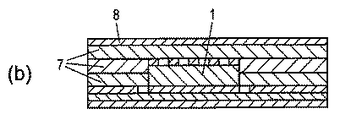
図3では図1の方法工程(c)に似た変形実施形態が示され、そのとき図1の実施形態における比較的厚さの小さい層或いは箔5とは対照的に、31と称される集積された電子部品に近接或いは接続する、隙間38を有する導電層或いは金属箔35が、図示された実施形態において実質的に、集積される電子部品31の例えば数100μmに及ぶ総高に一致する、比較的大きな厚さを備えることが明らかになる。
FIG. 3 shows an alternative embodiment similar to method step (c) of FIG. 1, which is then referred to as 31 in contrast to the relatively thin layer or
図3に示された、電子部品31が36と称される絶縁素材から成る層によって包囲された後、図1の実施形態に相似して、再び集積された電子部品31の導電層34及び、大きな厚さを備えそれに近接する層35が露出され、そのとき追加の導電層の配置によって、それが図1で示されたように、プリント基板或いはプリント基板中間体37の大きな部分領域に亘る良好な熱分散がなされる。
After the
図4の表示では、図2の実施形態のように、支持層42に向けられた接点43を有する集積されるべき電子部品41の配置或いは固定がなされ、そのとき固定のための接着層44が示される。
In the display of FIG. 4, as in the embodiment of FIG. 2, the
さらに、支持層42上に設けられる導電層或いは金属箔45は、集積されるべき電子部品41の接点43に相応する複数の凹部或いは隙間46を備え、電子部品41の配置或いは固定の際、それが矢印47で示されているように、接点42が導電層45の凹部或いは隙間46に嵌入する。
Further, the conductive layer or
さらに、前出の図1及び2に従っていくつかの中間工程を省略した図4において、集積されるべき電子部品41の絶縁素材から成る層48への埋め込み、及び支持層42の除去後、部品41の接点43及びそれに接続する導電層或いは金属箔45が露出されることが明らかになる。こうして図2の実施形態に相似して、更なる導電層が後に追加或いは配設され、それらが構造化されることによって、集積された電子部品41の接点43の簡単で確実な接触が行われる。電子部品41に近接する導電層或いは金属箔45は再び、支持層42が除去された後に露出される集積された電子部品41の接点43と同じ高さに位置する。
Further, in FIG. 4 in which some intermediate steps are omitted according to FIGS. 1 and 2 above, after embedding the
図5a及び5bに示された実施形態において、集積されるべき電子部品51は再び支持層52に支持され、そのとき部品51の接点は詳細に図示されない。前出の実施形態に相似して、電子部品51の層52上での固定は、再び接着剤の使用によってなされ得る。
In the embodiment shown in FIGS. 5a and 5b, the
集積されるべき電子部品51の寸法に合わせ、導電層或いは金属箔53は、再び相応の隙間或いは凹部60を備え、そのとき前出の実施形態に相似して、さらに絶縁素材から成る層54が導電層53の上に配置され、そのとき層或いは階層54も部品51の寸法に合わせた隙間を備える。製造されるべきプリント基板或いはプリント基板中間体の更なる層或いは階層は、55及び56によって示され、そのとき、層或いは階層56が導電性素材或いは導電性箔から成ることに対し、層或いは階層55は層54のように例えばプリプレグのような非導電性金属から成る。
Depending on the dimensions of the
図5bにおいて、集積されるべき部品51の集積のために、前出の実施形態と同様、詳細に図示されていない接点の接触の後に設けられる更なる層或いは階層57が、例えば支持層52又はその支持層52の代替となる層或いは階層、及び概略的に示された層或いは階層58によって形成される設けられる構造或いは構造化に対応し、凹部59を備え、それによって、そのように集積されるべき部品51の領域に設けられる構造を、製造されるべきプリント基板61或いは製造されるべきプリント基板中間体に完全に集積できることが示される。
In FIG. 5b, for the integration of the
図に示された接着剤層或いは接着層の替わりに、集積されるべき電子部品1、21、31、41、51の固定のために、集積されるべき部品の支持層に面した表面に設けられる、例えば水溶性フィルム或いは水溶性箔が、部品の暫時的な固定のために援用されることもできる。
Instead of the adhesive layer or adhesive layer shown in the figure, it is provided on the surface facing the support layer of the component to be integrated for fixing the
本発明は、少なくとも1つの電子部品をプリント基板又はプリント基板中間体に集積する方法、及びプリント基板又はプリント基板中間体に係る。 The present invention relates to a method for integrating at least one electronic component on a printed circuit board or printed circuit board intermediate, and to a printed circuit board or printed circuit board intermediate.
電子部品を備えた機器の製品機能の向上と、そのような電子部品の微細化の進展、及びプリント基板に実装される電子部品数の増加という関連において、複数の接点或いは端子を備え、それら接点の間隔をより縮小した、複数の電子部材を有する、より高性能のフィールド型或いはアレー型に形成された部品或いはパッケージが使用されている。そのような部品の固定又は接触のために、極めて細分化されたプリント基板の使用がますます必要とされ、そのとき使用されるべき部品とプリント基板の製品サイズが、そうした要素の厚さと面積という点において同時に縮小される場合、そのような電子部品を必要となる複数の接触部分を介してプリント基板上に実装或いは配置することが困難になること、或いはそのような接触部分の可能な分解能が限界に達することが予想されるのは必至である。 In relation to the improvement of the product function of a device equipped with electronic components, the progress of miniaturization of such electronic components, and the increase in the number of electronic components mounted on a printed circuit board, a plurality of contacts or terminals are provided. A part or package formed in a higher-performance field type or array type having a plurality of electronic members with a smaller interval is used. Increasingly, the use of highly fragmented printed circuit boards is required to secure or contact such components, and the components to be used at that time and the product size of the printed circuit board are referred to as the thickness and area of such elements. When simultaneously reduced in terms, it may be difficult to mount or place such electronic components on a printed circuit board through the required multiple contact portions, or the possible resolution of such contact portions. It is inevitable that the limit is expected to be reached.
このような問題を解決するために、これまでに例えば国際公開公報第03−065778号(特許文献1)、国際公開公報第03−065779号(特許文献2)、又は国際公開公報第2004−077902号(特許文献3)に示されているように、電子部品を少なくとも部分的にプリント基板に集積することが提案されている。 In order to solve such a problem, for example, International Publication No. 03-065778 (Patent Document 1), International Publication No. 03-065779 (Patent Document 2), or International Publication No. 2004-077902. (Patent Document 3), it has been proposed to at least partially integrate electronic components on a printed circuit board.
しかし、プリント基板に集積された電子部品或いは部材のこれらの公知の方法及び実施形態において、このような電子部品或いは部材を搭載するために、それぞれ凹部或いは孔がプリント基板の基礎部材の中に設けられ、さらに、そのとき部品をそのような孔中に配置する前にトレースが形成されるという不利が生じる。部品の接触のために、はんだ付け工程及びボンディング技術が使用され、そのとき通常接触部分はトレースの要素間及び電子部品の接触或いは接続部分間の異なった種類の素材間に生じる。 However, in these known methods and embodiments of electronic components or members integrated on a printed circuit board, recesses or holes are provided in the base member of the printed circuit board, respectively, for mounting such electronic components or members. Furthermore, there is the disadvantage that the traces are then formed before the part is placed in such a hole. Soldering processes and bonding techniques are used for component contact, where contact portions usually occur between different types of materials between trace elements and between electronic component contacts or connection portions.
特にこのようなシステムが大きな温度差或いは温度変化領域のある環境で使用される場合、 異なった温度による膨張係数を考慮し、接触或いは接続部分の領域で異なる素材を使用することにより、少なくとも1つの接触或いは接続部分の亀裂と、それによる部品の故障に繋がる可能性のある、機械的に或いは熱によって誘導された張力が生じる。その上、接触面を作成するために追加で必要となる穿孔、特にレーザー・ボーリングが部材に負担をかけることが想定できる。更に、作成されるべき凹部又は溝に埋め込まれた部品のトレースと接触面との接触が、はんだペースト又はボンディングワイヤによって妨げられ、或いは特に変動する温度による負担があるときの使用の際、確実に遂行されないという不利が生じる。 Especially when such a system is used in an environment with a large temperature difference or temperature change region, considering the expansion coefficient due to different temperatures, by using different materials in the area of contact or connection, at least one Mechanically or thermally induced tensions can occur that can lead to cracks in the contact or connection and thereby component failure. In addition, it can be assumed that additional drilling, especially laser boring, is necessary to create the contact surface, placing a burden on the member. In addition, the contact between the traces of the parts embedded in the recesses or grooves to be created and the contact surface is obstructed by the solder paste or bonding wires, or in particular when used when there is a burden due to fluctuating temperatures. The disadvantage of not being fulfilled arises.
補足として、場合によりプリント基板製造過程において生じる高圧と高温が、埋め込まれ接触される部材の負担となるという不利がある。更には、場合によってより強く帯電された電子部品の放熱が問題となる。 As a supplement, there is a disadvantage that the high pressure and high temperature that are generated in the printed circuit board manufacturing process may be a burden on the embedded and contacted members. Furthermore, in some cases, heat dissipation of a more strongly charged electronic component becomes a problem.
米国特許公開番号2008/0196930A1号明細書(特許文献4)及び米国特許公開番号2010/0214750A1号明細書(特許文献5)から、プリント基板の製造或いはプリント基板への電子部品の埋め込みの方法は知られており、それらの場合、集積或いは固定されるべき部品の接点に合わせた隙間を導電層内に設けるため、そのような接点の小さな寸法を考慮し、そのような隙間を形成及び設置することに、多大な労力を必要とする。 From US Patent Publication No. 2008 / 0196930A1 (Patent Document 4) and US Patent Publication No. 2010 / 0214750A1 (Patent Document 5), a method of manufacturing a printed circuit board or embedding electronic components in a printed circuit board is known. In these cases, in order to provide gaps in the conductive layer that match the contacts of the parts to be integrated or fixed, such gaps must be formed and installed taking into account the small dimensions of such contacts. In addition, a great deal of labor is required.
プリント基板への部品の埋め込みの変形された実施形態は、米国特許公開番号2009/0230541A1号明細書(特許文献6)、米国特許公開番号2006/0291173A1号明細書(特許文献7)又は米国特許公開番号2010/0044845A1号明細書(特許文献8)に見られ、それらの場合、例えば接触の簡略化が目標とされている。 Modified embodiments of embedding components in a printed circuit board are disclosed in US Patent Publication No. 2009 / 0230541A1 (Patent Document 6), US Patent Publication No. 2006 / 0291173A1 (Patent Document 7) or US Patent Publication. No. 2010 / 0044845A1 (patent document 8), in which case, for example, simplification of the contact is targeted.
従って本発明は、少なくとも1つの電子部品をプリント基板に集積する際の上述の問題を最小化又は解決することを目的とし、特に冒頭で述べられた種類の方法及び、製造されるべきプリント基板或いは製造されるべきプリント基板中間体を特に簡単に登録及び薄型化し、簡単な方法工程において、そのような電子部品をプリント基板或いはプリント基板中間体に簡単かつ確実に配置することができるプリント基板或いはプリント基板中間体を提供することを目的とする。 The invention is therefore aimed at minimizing or solving the above-mentioned problems in integrating at least one electronic component on a printed circuit board, in particular a method of the kind mentioned at the beginning and a printed circuit board to be manufactured or Printed circuit board or printed circuit board that can be easily and reliably placed and printed on a printed circuit board intermediate or a printed circuit board intermediate in a simple process step, especially with a simple registration and thinning of printed circuit board intermediates to be manufactured An object is to provide a substrate intermediate.
これらの課題を解決するために、冒頭に述べられた種類の方法は、実質的に以下の工程を含む。
− 電子部品を少なくとも暫定的に支持するための層を提供し、
− 層上に電子部品を固定し、そのとき電子部品の接点又は電子部品の表面に配置された導電層が支持層に配向され、
− 導電層を支持層上に、電子部品の接点又は電子部品の表面の導電層の高さに、固定されるべき電子部品の寸法と一致した少なくとも1つの隙間とともに配置し、そのとき部品に近接する導電層は金属箔、特に銅箔で形成され、
− 支持層上に固定される部品及び、部品に近接し支持層上に配置された導電層の少なくとも部分領域を、例えばプリプレグシート及び/又は樹脂のような絶縁素材によって、少なくとも部分的に包囲或いは被覆し、
− 電子部品の接点又は導電層、及び部品に近接し支持層上に配置された導電層の少なくとも部分領域を、支持層の除去後或いは除去によって露出し、
− 電子部品の接点又は導電層を、部品に近接する導電層と、少なくとも部分的に接触させる。
In order to solve these problems, a method of the kind mentioned at the outset essentially comprises the following steps.
-Providing a layer for at least provisional support of the electronic component;
The electronic component is fixed on the layer, at which time the contact of the electronic component or the conductive layer disposed on the surface of the electronic component is oriented to the support layer;
The conductive layer is placed on the support layer at the contact point of the electronic component or at the height of the conductive layer on the surface of the electronic component, with at least one gap matching the size of the electronic component to be fixed, then in proximity to the component The conductive layer is made of metal foil, especially copper foil,
-At least partly enclosing or at least partially enclosing the component to be fixed on the support layer and the conductive layer disposed on the support layer adjacent to the component, for example by an insulating material such as a prepreg sheet and / or resin; Coat,
The contact or conductive layer of the electronic component and at least a partial region of the conductive layer disposed on the support layer adjacent to the component are exposed after or by removal of the support layer;
The contact or conductive layer of the electronic component is at least partially in contact with the conductive layer proximate to the component;
本発明により、固定されるべき電子部品の寸法と一致した少なくとも1つの隙間を有する導電層を支持層上に配置することにより、そのような導電層を埋め込まれるべき電子部品の接点又は導電層と同じ高さに配置することができ、それによる更なる結果として、この導電層を集積された電子部品と簡単に接触させることができる。さらに、この導電層を集積されるべき電子部品の後にで出されるべき表面と同じ高さに配置することによって、製造されるべきプリント基板或いは製造されるべきプリント基板中間体の総厚を低減することが可能になる。 According to the present invention, by placing on the support layer a conductive layer having at least one gap that matches the dimensions of the electronic component to be fixed, such a contact or conductive layer of the electronic component to be embedded They can be arranged at the same height, and as a further consequence, this conductive layer can be easily brought into contact with the integrated electronic component. Furthermore, the total thickness of the printed circuit board to be manufactured or the printed circuit board intermediate to be manufactured is reduced by arranging this conductive layer at the same height as the surface to be brought out after the electronic component to be integrated. It becomes possible.
その上、このように導電層を実質的に集積されるべき電子部品の露出されるべき表面と同じ高さに設置することにより、部品をそれに近接する導電層の領域に接触させることが簡単になり、従って集積されるべき電子部品の配置を単純化或いは改善し、かつそれの接触を単純化したプリント基板或いはプリント基板中間体が総合的に実現される。更に導電層の隙間或いは凹部によって、電子部品の登録或いは配列を、その配置或いは固定の際に、単純化或いは容易にすることができる。 Moreover, by placing the conductive layer substantially at the same height as the exposed surface of the electronic component to be integrated, it is easy to bring the component into contact with the region of the conductive layer adjacent to it. Therefore, a printed circuit board or a printed circuit board intermediate in which the arrangement of electronic components to be integrated is simplified or improved and the contact thereof is simplified is realized in a comprehensive manner. Further, the registration or arrangement of electronic components can be simplified or facilitated by the gaps or recesses of the conductive layer when the electronic components are arranged or fixed.
そこで本発明では、搭載されるべき或いは支持されるべき部品に近接する部分領域への導電層の設置或いは配置を簡略化するために、部品に近接する導電層が金属箔、特に銅箔で形成されることが提案される。そのような金属箔、特に銅箔は、相応に望ましい厚さで設置されることができ、簡単な、プリント基板製造の際に知られている方法工程で配置され、このようなプリント基板又はプリント基板中間体の他の層或いは要素と接続されることができる。 Therefore, in the present invention, in order to simplify the installation or arrangement of the conductive layer in a partial region close to the component to be mounted or supported, the conductive layer close to the component is formed of a metal foil, particularly a copper foil. It is suggested that Such metal foils, in particular copper foils, can be installed in correspondingly desirable thicknesses and are arranged in a simple manner known in the manufacture of printed circuit boards, such printed circuit boards or printed boards. It can be connected to other layers or elements of the substrate intermediate.
集積されるべき電子部品の簡単で確実な固定のために、電子部品を接着剤、接着箔、部品の接着膜などを介して支持層上に固定することが、本発明の方法の好適な実施形態によって行われ、このとき接着層は支持層とともに除去される。従って特に更なる処理工程に応じて、電子部品を支持層上に固定するための異なった手段が用いられ、そのときそれらが相応な薄さで使用できるのみならず、集積されるべき部品の導電層と接点が、部品が包囲された後に、簡単で確実に露出されることができる。 For the simple and reliable fixing of electronic components to be integrated, it is preferable to fix the electronic component on the support layer via an adhesive, an adhesive foil, an adhesive film of the component, etc. The adhesive layer is removed together with the support layer. Thus, depending on the further processing steps, different means for fixing the electronic components on the support layer are used, in which case they can not only be used in a suitable thickness, but also the conductivity of the components to be integrated. The layers and contacts can be easily and reliably exposed after the part is enclosed.
特に製造されるべきプリント基板又はプリント基板中間体の総厚の低減に関しては、接着層又は接着箔又は塗装膜が、最大15μm、特に0.1から10μmの厚さに形成されることが、更なる好適な実施形態によって提案される。本発明においては、従って接着層又は接着箔が比較的厚さが小さくて充分であり、そのとき接着層又は接着箔のこのように小さい厚さにも関わらず、電子部品の支持層上での確実な接着或いは固定が可能になる。 In particular with regard to reducing the total thickness of the printed circuit board or printed circuit board intermediate to be produced, it is further preferred that the adhesive layer or adhesive foil or paint film is formed to a thickness of up to 15 μm, in particular from 0.1 to 10 μm. Proposed by the preferred embodiment. In the present invention, therefore, it is sufficient that the adhesive layer or the adhesive foil has a relatively small thickness, and at that time, despite the small thickness of the adhesive layer or the adhesive foil, the adhesive layer or adhesive foil on the support layer of the electronic component is used. Secure bonding or fixing becomes possible.
さらに、特に簡単で確実な接着層の形成のため、本発明の方法の更なる好適な実施形態に対応するように、接着層をインクジェット、フレックス、凹版、又はオフセット印刷によって塗着することが提案される。 Furthermore, for the formation of a particularly simple and reliable adhesive layer, it is proposed to apply the adhesive layer by ink jet, flex, intaglio or offset printing so as to correspond to further preferred embodiments of the method of the invention. Is done.
特に集積されるべき電子部品の使用目的及び/又は、部品の接点又は導電層の支持層に対する配向に応じて、金属箔、特に銅箔が、特に導電性構造のために、最大15μm、特に0.1から10μmの厚さに形成されることが、更なる好適な実施形態によって提案される。このように、金属箔、特に銅箔に相応する薄さにおいて、集積されるべき電子部品の接点と、特に構造化された薄い導電性層との簡単かつ確実な接触が提供される。 Depending on the intended use of the electronic component to be integrated and / or the orientation of the contact of the component or the conductive layer relative to the support layer, metal foils, in particular copper foils, can be up to 15 μm, in particular 0, especially for conductive structures. It is proposed by a further preferred embodiment to be formed to a thickness of 1 to 10 μm. In this way, simple and reliable contact between the contacts of the electronic components to be integrated and the thin structured conductive layer, in particular, is provided in a thickness corresponding to a metal foil, in particular a copper foil.
特に使用或いは作動中に、相応に放散されなければならない比較的大きな熱量を発生させる高性能の集積されるべき部品の場合、集積されるべき電子部品の側面領域或いは周縁領域における良好な放熱が必要であり、最大500μm、特に約35μmから400μmの厚さを有する、特に放熱のための金属箔、特に銅箔が形成されることが、本発明の方法の変形された好適な実施形態によって提案される。このような比較的大きな厚さによって、集積されるべき電子部品は、実質的にその全周に亘ってそのような相応の良好な熱伝導性のある金属箔によって包設されるため、集積されるべき電子部品が発生する熱を、プリント基板或いはプリント基板中間体のより広範な面或いは領域に亘って分散させることが可能になる。 Good heat dissipation in the side or peripheral area of the electronic component to be integrated, especially in the case of high performance integrated components that generate a relatively large amount of heat that must be dissipated accordingly during use or operation It is proposed by a modified preferred embodiment of the method of the invention that a metal foil, in particular a copper foil, in particular for heat dissipation, having a thickness of up to 500 μm, in particular about 35 μm to 400 μm, is formed. The Due to such a relatively large thickness, the electronic components to be integrated are substantially integrated because they are surrounded by such a correspondingly good metal foil with good thermal conductivity. The heat generated by the electronic components to be made can be distributed over a wider area or area of the printed circuit board or printed circuit board intermediate.
既に上述したように、集積されるべき電子部品と、実質的に集積されるべき電子部品の接点の高さ或いはレベルに設置された、追加の導電層との簡単かつ確実な方法での接触がなされ、そのときこの関連において、部品に近接した導電層が構造化された層によって形成され、そのとき導電層は特にラミネート後に構造化されることが、更なる好適な実施形態によって提案される。 As already mentioned above, there is a simple and reliable contact between the electronic component to be integrated and the additional conductive layer placed at the height or level of the contact of the electronic component to be substantially integrated. In this connection, it is proposed according to a further preferred embodiment that in this connection a conductive layer proximate to the part is formed by the structured layer, where the conductive layer is then structured especially after lamination.
埋め込まれるべき電子部品に近接した導電層或いは導電性層の、特に簡単かつ確実な接触のために、支持層に向けられた電子部品の接点の場合、支持層の除去後、接点を構造化された導電層と接触或いは接続させることが、更なる好適な実施形態によって提案される。 In the case of contacts of electronic components directed to the support layer, especially for easy and reliable contact of the conductive layer or conductive layer close to the electronic component to be embedded, the contact is structured after removal of the support layer. It is proposed by a further preferred embodiment to contact or connect to another conductive layer.
同様に上記に既に示されたように、良好な放熱のために、通常部品に近接した比較的厚さの大きな導電層が設けられ、そのとき導電層を、特に作動中に高熱量を発生させる電子部品と、それに近接する導電層を接触させるために、本発明の方法の更なる好適な実施形態に対応するように、電子部品の導電層の露出後に、近接する導電層との実質的な全面接触が行われることが提案される。 Similarly, as already indicated above, for good heat dissipation, a conductive layer with a relatively large thickness is usually provided in close proximity to the component, which then generates a high amount of heat, especially during operation. In order to bring the electronic component into contact with the conductive layer proximate to it, substantially corresponding to the adjacent conductive layer after exposure of the conductive layer of the electronic component, corresponding to a further preferred embodiment of the method of the invention. It is suggested that full contact be made.
望ましい放熱を行うために、導電性素材、特に熱伝導性素材から成る層の全面接触がなされることが、この関連において好適に提案される。 In order to achieve the desired heat dissipation, it is preferably proposed in this connection that the entire surface of a layer made of a conductive material, in particular a thermally conductive material, is made.
特に、簡単かつ確実な方法で、集積されるべき電子部品の露出後、該当する更なる層との接触が可能になるプリント基板中間体の製造の際、電子部品の導電層又は接点の露出及び、それに近接する導電層との接触の後、プリント基板の更なる層及び/又は構造化が形成される、或いは行われることが、プリント基板の完成のために提案される。 In particular, in the production of printed circuit board intermediates that allow contact with the relevant further layers after exposure of the electronic components to be integrated in a simple and reliable manner, the exposure of the conductive layers or contacts of the electronic components and It is proposed for the completion of the printed circuit board that further layers and / or structuring of the printed circuit board are formed or performed after contact with the conductive layer adjacent thereto.
集積されるべき電子部品の領域の構造に対応し、特にその部品及び/又はそれと関連した要素を製造されるべきプリント基板に埋め込むために、プリント基板の少なくとも1枚の更なる層が、凹部或いは溝を、集積された電子部品の領域に設けることが、本発明の方法の更なる好適な実施形態によって提案される。 In order to correspond to the structure of the area of the electronic component to be integrated and in particular to embed the component and / or its associated elements in the printed circuit board to be manufactured, at least one further layer of the printed circuit board is provided with a recess or Providing grooves in the area of the integrated electronic component is proposed by a further preferred embodiment of the method of the invention.
その上、冒頭に述べられた課題を解決するために、冒頭に述べられた種類のプリント基板又はプリント基板中間体は実質的に、例えばプリプレグシート及び/又は樹脂のような絶縁素材によって少なくとも部分的に包囲され、又はそれによって被覆された電子部品と、電子部品の接点又は電子部品の表面の導電層の高さに配置され、部品に近接する導電層から成り、そのとき部品に近接する導電層は、固定されるべき電子部品の寸法に一致した少なくとも1つの隙間を備え、そのとき電子部品の接点又は電子部品の表面に設置された導電層は、部品に近接した導電層と連結される、或いは連結可能であり、そのとき部品に近接する導電層が金属箔、特に銅箔によって形成され、又そのとき支持層上に固定された部品及び部品に近接し、支持層上に配置された導電層の少なくとも部分領域が、例えばプリプレグシート及び/又は樹脂のような絶縁素材で、少なくとも部分的に包囲或いは被覆されている。 Moreover, in order to solve the problems mentioned at the outset, a printed circuit board or printed circuit board intermediate of the kind mentioned at the outset is substantially at least partly by an insulating material such as a prepreg sheet and / or a resin. An electronic component surrounded by or covered by an electronic component and a contact layer of the electronic component or a conductive layer adjacent to the component, disposed at the height of the conductive layer on the surface of the electronic component, and then the conductive layer adjacent to the component Comprises at least one gap corresponding to the dimension of the electronic component to be fixed, at which time the contact of the electronic component or the conductive layer placed on the surface of the electronic component is connected to the conductive layer proximate to the component; Alternatively, the conductive layer proximate to the component is formed by a metal foil, in particular copper foil, and is then proximate to the component and component fixed on the support layer, and the support layer At least partial areas of the arranged conductive layer is, for example, an insulating material such as prepreg sheets and / or resin, is at least partially surrounded or covered.
上記に言及したように、このようにしてこのようなプリント基板又はプリント基板中間体の簡単で確実な製造がなされ、そのとき特に、部品に近接する、固定されるべき電子部品の寸法に一致した隙間を備えた層によって、集積されるべき電子部品の簡単で確実な登録或いは設置、及び製造されるべきプリント基板又は製造されるべきプリント基板中間体の全高の低減或いは最小化が、集積されるべき電子部品の露出された表面の相応に簡単な接触の際に可能となる。 As mentioned above, a simple and reliable production of such a printed circuit board or printed circuit board intermediate is thus achieved, in particular in accordance with the dimensions of the electronic component to be fixed, in particular close to the component. The layer with gaps integrates the simple and reliable registration or installation of the electronic components to be integrated and the reduction or minimization of the total height of the printed circuit board to be manufactured or the printed circuit board intermediate to be manufactured. This is possible with a correspondingly simple contact of the exposed surface of the electronic component.
さらに、集積されるべき電子部品の接点との簡単で確実な接触のために、部品に近接する導電層を金属箔、特に銅箔によって形成することが提案される。 Furthermore, it is proposed to form a conductive layer close to the component with a metal foil, in particular a copper foil, for simple and reliable contact with the contacts of the electronic component to be integrated.
特に集積されるべき電子部品の使用目的及び/又は集積されるべき電子部品の接点又はその導電層の支持層に対する配向に従い、金属箔、特に銅箔が、特に導電性構造のために、最大15μm、特に約0.1μmから10μmの厚さを有することが、更なる好適な実施形態によって提案される。このようにして、製造されるべきプリント基板或いはプリント基板中間体の総厚の更なる低減或いは最小化にも貢献する、薄型の導電或いは導電性構造が提供される。 Depending on the intended use of the electronic component to be integrated and / or the contact of the electronic component to be integrated or the orientation of its conductive layer with respect to the support layer, metal foils, in particular copper foils, can be up to 15 μm, especially for conductive structures. In particular, it is proposed by a further preferred embodiment to have a thickness of about 0.1 μm to 10 μm. In this way, a thin conductive or conductive structure is provided that also contributes to further reducing or minimizing the total thickness of the printed circuit board or printed circuit board intermediate to be manufactured.
相応の薄い箔によって、集積されるべき部品の接点との接触のための構造化された導電性層が提供されることができる一方、場合によって高熱量を発生させる電子部品の作動或いは使用中、発生する熱のより広範な面或いは領域に亘る分散が必要或いは有益となり、そのときこの関連において、本発明のプリント基板又は本発明のプリント基板中間体の更なる好適な実施形態に対応するように、特に放熱のための金属箔、特に銅箔が、最大500μm、特に約35μmから400μmの厚さを有することが提案される。 Corresponding thin foils can provide a structured conductive layer for contact with the contacts of the components to be integrated, while in operation or use of electronic components that generate high heat, in some cases, Dispersion of the generated heat over a wider area or region becomes necessary or beneficial, in this context, so as to correspond to further preferred embodiments of the printed circuit board of the present invention or of the printed circuit board intermediate of the present invention. In particular, it is proposed that metal foils, in particular copper foils, for heat dissipation have a maximum thickness of 500 μm, in particular from about 35 μm to 400 μm.
集積されるべき電子部品の、支持層に向けられた接点との確実な連結のために、更なる好適な実施形態によって、電子部品の接点との連結或いは接触のために、部品に近接する導電層が構造化された導電層によって形成されることが提案される。 For a secure connection of the electronic component to be integrated with the contact directed to the support layer, according to a further preferred embodiment, a conductive material close to the component for connection or contact with the contact of the electronic component is provided. It is proposed that the layer is formed by a structured conductive layer.
それに対し、場合により使用中に高熱量を発生させる電子部品の簡単かつ確実な放熱のために、更なる変形された好適な実施形態によって、電子部品の導電層との連結或いは接触のために、それに近接する導電層との実質的な全面接触が行われることが提案される。 On the other hand, for easy and reliable heat dissipation of the electronic component that generates a high amount of heat during use, according to a further modified preferred embodiment, for connection or contact with the conductive layer of the electronic component, It is proposed that substantially full contact is made with the adjacent conductive layer.
さらに、確実な放熱を補助するために、導電性素材、特に伝熱性素材から成る層の全面接触がなされることが好適に提案される。 Furthermore, in order to assist reliable heat dissipation, it is preferably proposed that the entire surface of a layer made of a conductive material, particularly a heat conductive material, is made.
本発明は、以下の通り添付の図面に概略的に示された実施形態を参照してより詳細に説明される。 The invention will be described in more detail with reference to the embodiments schematically shown in the accompanying drawings as follows.
添付の図面においては、個々の層或いは階層の相対的な厚さ、及びそのような層と階層の寸法が、特に集積されるべき電子部品と比較して正確な尺寸ではなく、部分的に明瞭化のために厚さ或いは寸法が、過度に大きく表示されていることに概して留意されたい。さらに、通常比較的多数のそのような接点を備えた部品が示されることとは対照的に、概して集積されるべき電子部品の少数の接点のみが示されている。 In the accompanying drawings, the relative thicknesses of the individual layers or layers, and the dimensions of such layers and layers, are not particularly accurate as compared to the electronic components to be integrated, but are partly clear. It is generally noted that the thickness or dimensions are displayed too large for simplicity. Furthermore, in general, only a small number of contacts of an electronic component to be integrated are shown, as opposed to showing a component with a relatively large number of such contacts.
図1では、方法工程(a)において、概して1と称される、製造されるべきプリント基板或いは製造されるべきプリント基板中間体に集積される部品の配置或いは固定がなされ、そのとき電子部品1の支持或いは固定は支持層2上で行われ、支持層2上での固定のために接着剤層3が設けられる。
In FIG. 1, in method step (a), a component to be manufactured or a component integrated on a printed circuit board intermediate to be manufactured, which is generally referred to as 1, is arranged or fixed. Is supported or fixed on the
図1に示される実施形態では、電子部品1が導電或いは導電性層4を、支持層2或いは接着剤層3に向けている。さらに、配置或いは集積されるべき電子部品1の寸法に合わせて凹部或いは隙間を形成した、特に金属箔或いは銅箔5である導電層が、同様に支持層2上に固定されていることが、方法工程(a)において明らかになる。
In the embodiment shown in FIG. 1, the
正確でない尺寸の層厚同様、層5の隙間或いは凹部6の横方向の間隔も、搭載されるべき或いは埋め込まれるべき電子部品1の寸法に対し、誇張された大きさで表示されている。
Like the inaccurate layer thickness, the gaps in the
導電層4を介した電子部品1の固定及びそれに近接する導電層或いは金属箔5の固定は、例示的に、例えば15μm未満、特に5μm未満の相応に厚さの微小な接着剤を介してなされる。このような接着層は、例えばインクジェット、フレックス、凹版又はオフセット印刷法によって塗着されることができる。
The fixing of the
電子部品1及び導電層或いは箔5を支持層2上に配置或いは固定した後、工程(b)において、例えば複数のプリプレグシートのような絶縁素材から成る複数の概略的に示された層7の配置がなされ、そのとき追加でもう1枚の導電層8も示される。
After placing or fixing the
電子部品1を包囲し、或いはその上に重層する複数の層7或いは8をこのように配置した後、工程(c)において、埋め込まれるべき電子部品1のラミネート及び完全な包囲がなされ、そのときラミネート工程(c)中に個々の層或いは階層7の、絶縁素材から成る共通層或いは階層9への接続がなされる。
After the
工程(c)において埋め込まれるべき電子部品1がそのように包囲された後、工程(d)において支持層2及び接着層3の除去がなされ、従って導電層5のみならず、集積される電子部品1の導電層4も露出する。
After the
電子部品の接点10の逆側に位置する導電層4は、実質的に導電層5と同じ高さ或いはレベルにあり、従って方法工程(d)において集積すべき電子部品1の表面が完全に露出されることが、ここで特に明らかになる。
The conductive layer 4 located on the opposite side of the
概略的に11と称されるプリント基板或いはプリント基板中間体11の更なる構成のために、集積された電子部品1の導電層4及び導電層或いは金属箔5の露出の後、更なる導電層12及び13の増設がなされ、そのとき方法工程(e)において、さらに、埋め込まれた電子部品1の接点10の、例として導電性素材が充填された穿孔14との接触を介しての接触が示されている。
Due to the further construction of the printed circuit board or printed circuit board intermediate 11, generally referred to as 11, after the exposure of the conductive layer 4 and the conductive layer or
さらに図1の表示から、集積された電子部品1の導電層4が、例えば良好な放熱或いは熱放散のために、追加された導電層12と実質的に全面的に接続され、熱をより広範な部分領域に分散させるために、それと近接し同じ高さに位置する導電層或いは金属箔5の部分領域と全面接続を介して接続されていることが明らかになる。
Further, from the display of FIG. 1, the conductive layer 4 of the integrated
図2には電子部品の埋め込み方法の変形実施形態が示され、そのとき再度(a)と称される第1の方法工程において、埋め込まれるべき電子部品21が支持層22上に、接着剤層23を介して固定される。
FIG. 2 shows a modified embodiment of the method for embedding electronic components, in which the
図1の実施形態とは対照的に、集積されるべき電子部品21の支持層22或いは接着層23上での固定は、支持層22に向けられた接点24によってなされる。
In contrast to the embodiment of FIG. 1, the fixing of the
図1の実施形態に相似して、支持層22或いは接着層23上に再び、集積されるべき電子部品21の外形寸法に合わせた隙間或いは凹部26を備えた、導電層或いは金属箔25が設けられる。
Similar to the embodiment of FIG. 1, a conductive layer or
図1の方法工程(c)に相似して、図2では同様に(c)において、詳細に図示されていない絶縁素材から成る複数の層の配置の後、例えばラミネート工程によって、集積された電子部品21の絶縁素材から成る被覆27への完全な埋め込みが行われ、そのとき図1の実施形態と同様に導電層28が示される方法工程が表される。
Similar to method step (c) of FIG. 1, in FIG. 2 as well, in FIG. 2 (c), after the placement of a plurality of layers of insulating material not shown in detail, the integrated electrons, for example, by a lamination step A complete embedding of the
図2の工程(c)に従った電子部品21のそのような埋め込みの後、前出の実施形態に相似し、工程(d)において、再び集積された電子部品21の接点24及び近接する導電層或いは金属箔25が露出される。接点24及び、導電性の、特に構造化された層25が再び、実質的に同じ高さ或いは同じレベルに位置し、従って前述の実施形態に相似して、この場合 接点24を備えた集積された電子部品の表面、及び導電層或いは金属箔25の露出が再び可能になる。
After such embedding of the
再び(e)と称される工程では、開口部或いは穿孔31と32及び集積された電子部品21の接点24との接触によって示されるように、更なる導電層29及び30が増設され、それらの構造化もなされる。
In the process again referred to as (e), additional
図3では図1の方法工程(c)に似た変形実施形態が示され、そのとき図1の実施形態における比較的厚さの小さい層或いは箔5とは対照的に、31と称される集積された電子部品に近接或いは接続する、隙間38を有する導電層或いは金属箔35が、図示された実施形態において実質的に、集積される電子部品31の例えば数100μmに及ぶ総高に一致する、比較的大きな厚さを備えることが明らかになる。
FIG. 3 shows an alternative embodiment similar to method step (c) of FIG. 1, which is then referred to as 31 in contrast to the relatively thin layer or
図3に示された、電子部品31が36と称される絶縁素材から成る層によって包囲された後、図1の実施形態に相似して、再び集積された電子部品31の導電層34及び、大きな厚さを備えそれに近接する層35が露出され、そのとき追加の導電層の配置によって、それが図1で示されたように、プリント基板或いはプリント基板中間体37の大きな部分領域に亘る良好な熱分散がなされる。
After the
図4の表示では、図2の実施形態のように、支持層42に向けられた接点43を有する集積されるべき電子部品41の配置或いは固定がなされ、そのとき固定のための接着層44が示される。
In the display of FIG. 4, as in the embodiment of FIG. 2, the
さらに支持層42上に設けられる導電層或いは金属箔45は、集積されるべき電子部品41の接点43に相応する複数の凹部或いは隙間46を備え、電子部品41の配置或いは固定の際、それが矢印47で示されているように、接点42が導電層45の凹部或いは隙間46に嵌入する。
Further, the conductive layer or
さらに、前出の図1及び2に従っていくつかの中間工程を省略した図4において、集積されるべき電子部品41の絶縁素材から成る層48への埋め込み、及び支持層42の除去後、部品41の接点43及びそれに接続する導電層或いは金属箔45が露出されることが明らかになる。こうして図2の実施形態に相似して、更なる導電層が後に追加或いは配設され、それらが構造化されることによって、集積された電子部品41の接点43の簡単で確実な接触が行われる。電子部品41に近接する導電層或いは金属箔45は再び、支持層42が除去された後に露出される集積された電子部品41の接点43と同じ高さに位置する。
Further, in FIG. 4 in which some intermediate steps are omitted according to FIGS. 1 and 2 above, after embedding the
図5a及び5bに示された実施形態において、集積されるべき電子部品51は再び支持層52に支持され、そのとき部品51の接点は詳細に図示されない。前出の実施形態に相似して、電子部品51の層52上での固定は、再び接着剤の使用によってなされ得る。
In the embodiment shown in FIGS. 5a and 5b, the
集積されるべき電子部品51の寸法に合わせ、導電層或いは金属箔53は、再び相応の隙間或いは凹部60を備え、そのとき前出の実施形態に相似して、さらに絶縁素材から成る層54が導電層53の上に配置され、そのとき層或いは階層54も部品51の寸法に合わせた隙間を備える。製造されるべきプリント基板或いはプリント基板中間体の更なる層或いは階層は、55及び56によって示され、そのとき、層或いは階層56が導電性素材或いは導電性箔から成ることに対し、層或いは階層55は層54のように例えばプリプレグのような非導電性金属から成る。
Depending on the dimensions of the
図5bにおいて、集積されるべき部品51の集積のために、前出の実施形態と同様、詳細に図示されていない接点の接触の後に設けられる更なる層或いは階層57が、例えば支持層52又はその支持層52の代替となる層或いは階層、及び概略的に示された層或いは階層58によって形成される設けられる構造或いは構造化に対応し、凹部59を備え、それによって、そのように集積されるべき部品51の領域に設けられる構造を、製造されるべきプリント基板61或いは製造されるべきプリント基板中間体に完全に集積できることが示される。
In FIG. 5b, for the integration of the
図に示された接着剤層或いは接着層の替わりに、集積されるべき電子部品1、21、31、41、51の固定のために、集積されるべき部品の支持層に面した表面に設けられる、例えば水溶性フィルム或いは水溶性箔が、部品の暫時的な固定のために援用されることもできる。
Instead of the adhesive layer or adhesive layer shown in the figure, it is provided on the surface facing the support layer of the component to be integrated for fixing the
Claims (20)
− 電子部品(1、21、31、41、51)を少なくとも暫定的に支持するための層(2、22、32、42、52)を提供し、
− 前記層(2、22、32、42、52)上に前記電子部品(1、21、31、41、51)を固定し、そのとき前記電子部品(21、41)の接点(24、23)又は前記電子部品(1、3)の表面に配置された導電層(4、34)が支持層(2、22、32、42、52)に配向され、
− 導電層(5、25、35、45、53)を、固定されるべき前記電子部品(1、21、31、41、51)及び/又は前記部品(21、41)の前記支持層に向けられた前記接点(24、43)の寸法と一致した少なくとも1つの隙間(6、26、38、46、60)とともに、前記支持層上(51)に配置し、
− 前記支持層に固定される前記部品(1、21、31、41、51)及び、前記部品(1、21、31、41、51)に近接し、前記支持層(2、22,32,42,52)上に配置された前記導電層(5、25、35、45、53)の少なくとも部分領域を、例えばプリプレグシート及び/又は樹脂のような絶縁素材(7、9、27、36、48、54、55)で少なくとも部分的に包囲或いは被覆し、
− 前記電子部品の前記接点(24、43)又は前記導電層(4、34)、及び前記部品に近接し、前記支持層(2、22、32、42、52)上に配置された前記導電層(5、25、35、45)の少なくとも部分領域を、前記支持層(2、22、32、42)の除去後に或いは除去によって露出し、
− 前記電子部品(1、21、31、41、51)の前記接点(24、43)又は前記導電層(4、34)を前記部品に近接する前記導電層(5、25、35、45、53)と少なくとも部分的に接触させる、を含む方法。 A method for integrating at least one electronic component on a printed circuit board or printed circuit board intermediate, comprising the following steps:
-Providing layers (2, 22, 32, 42, 52) for at least provisional support of the electronic components (1, 21, 31, 41, 51);
-Fixing the electronic components (1, 21, 31, 41, 51) on the layers (2, 22, 32, 42, 52), at which time the contacts (24, 23) of the electronic components (21, 41); ) Or a conductive layer (4, 34) disposed on the surface of the electronic component (1, 3) is oriented to the support layer (2, 22, 32, 42, 52),
The conductive layer (5, 25, 35, 45, 53) is directed to the electronic component (1, 21, 31, 41, 51) to be fixed and / or the support layer of the component (21, 41); Disposed on the support layer (51), together with at least one gap (6, 26, 38, 46, 60) corresponding to the size of the contact (24, 43) formed,
-The component (1, 21, 31, 41, 51) fixed to the support layer and the component (1, 21, 31, 41, 51) in proximity to the support layer (2, 22, 32, 42, 52) at least a partial region of the conductive layer (5, 25, 35, 45, 53) disposed on the insulating material (7, 9, 27, 36, eg, prepreg sheet and / or resin). 48, 54, 55) at least partially surrounding or covering,
-The contact (24, 43) or the conductive layer (4, 34) of the electronic component, and the conductive layer disposed on the support layer (2, 22, 32, 42, 52) proximate to the component; Exposing at least a partial region of the layer (5, 25, 35, 45) after or by removal of the support layer (2, 22, 32, 42);
The contact point (24, 43) or the conductive layer (4, 34) of the electronic component (1, 21, 31, 41, 51) is the conductive layer (5, 25, 35, 45, close to the component); 53) at least partially in contact with.
Applications Claiming Priority (3)
| Application Number | Priority Date | Filing Date | Title |
|---|---|---|---|
| ATGM41/2011U AT13055U1 (en) | 2011-01-26 | 2011-01-26 | METHOD FOR INTEGRATING AN ELECTRONIC COMPONENT INTO A CONDUCTOR PLATE OR A PCB INTERMEDIATE PRODUCT AND PCB OR INTERMEDIATE CIRCUIT PRODUCT |
| ATGM41/2011 | 2011-01-26 | ||
| PCT/AT2012/000011 WO2012100274A1 (en) | 2011-01-26 | 2012-01-24 | Method for integrating an electronic component into a printed circuit board or a printed circuit board intermediate product, and printed circuit board or printed circuit board intermediate product |
Publications (2)
| Publication Number | Publication Date |
|---|---|
| JP2014505367A true JP2014505367A (en) | 2014-02-27 |
| JP5988178B2 JP5988178B2 (en) | 2016-09-07 |
Family
ID=46579374
Family Applications (1)
| Application Number | Title | Priority Date | Filing Date |
|---|---|---|---|
| JP2013550705A Active JP5988178B2 (en) | 2011-01-26 | 2012-01-24 | Method for integrating electronic components into printed circuit board or intermediate product of printed circuit board, and printed circuit board or intermediate product of printed circuit board |
Country Status (6)
| Country | Link |
|---|---|
| US (1) | US9253888B2 (en) |
| EP (1) | EP2668835B1 (en) |
| JP (1) | JP5988178B2 (en) |
| CN (2) | CN103348777B (en) |
| AT (1) | AT13055U1 (en) |
| WO (1) | WO2012100274A1 (en) |
Families Citing this family (19)
| Publication number | Priority date | Publication date | Assignee | Title |
|---|---|---|---|---|
| AT13055U1 (en) * | 2011-01-26 | 2013-05-15 | Austria Tech & System Tech | METHOD FOR INTEGRATING AN ELECTRONIC COMPONENT INTO A CONDUCTOR PLATE OR A PCB INTERMEDIATE PRODUCT AND PCB OR INTERMEDIATE CIRCUIT PRODUCT |
| CN203206586U (en) * | 2013-02-27 | 2013-09-18 | 奥特斯(中国)有限公司 | A semi-finished product used for producing a printed circuit board |
| AT514074B1 (en) * | 2013-04-02 | 2014-10-15 | Austria Tech & System Tech | Method for producing a printed circuit board element |
| AT514564B1 (en) * | 2013-07-04 | 2015-02-15 | Austria Tech & System Tech | Method for contacting and rewiring |
| WO2015077808A1 (en) | 2013-11-27 | 2015-06-04 | At&S Austria Technologie & Systemtechnik Aktiengesellschaft | Circuit board structure |
| AT515101B1 (en) | 2013-12-12 | 2015-06-15 | Austria Tech & System Tech | Method for embedding a component in a printed circuit board |
| JP2015146346A (en) * | 2014-01-31 | 2015-08-13 | イビデン株式会社 | Multilayer wiring board |
| AT515447B1 (en) | 2014-02-27 | 2019-10-15 | At & S Austria Tech & Systemtechnik Ag | Method for contacting a component embedded in a printed circuit board and printed circuit board |
| US11523520B2 (en) | 2014-02-27 | 2022-12-06 | At&S Austria Technologie & Systemtechnik Aktiengesellschaft | Method for making contact with a component embedded in a printed circuit board |
| GB2524791B (en) * | 2014-04-02 | 2018-10-03 | At & S Austria Tech & Systemtechnik Ag | Placement of component in circuit board intermediate product by flowable adhesive layer on carrier substrate |
| JP6233524B2 (en) * | 2014-09-04 | 2017-11-22 | 株式会社村田製作所 | Component built-in board |
| TWI611523B (en) * | 2014-09-05 | 2018-01-11 | 矽品精密工業股份有限公司 | Semiconductor package manufacturing method |
| KR102194718B1 (en) * | 2014-10-13 | 2020-12-23 | 삼성전기주식회사 | Embedded board and method of manufacturing the same |
| US20170084594A1 (en) * | 2015-09-20 | 2017-03-23 | Qualcomm Incorporated | Embedding die technology |
| EP3206229B1 (en) | 2016-02-09 | 2020-10-07 | AT & S Austria Technologie & Systemtechnik Aktiengesellschaft | Methods of manufacturing flexible electronic devices |
| EP3300105B1 (en) * | 2016-09-26 | 2022-07-13 | Infineon Technologies AG | Semiconductor power module and method for manufacturing the same |
| CN207022286U (en) * | 2017-01-13 | 2018-02-16 | 奥特斯(中国)有限公司 | For manufacturing the semi-finished product and its part bearing part of part bearing part |
| US11953061B2 (en) * | 2019-04-14 | 2024-04-09 | The Johns Hopkins University | Clutch system with phase changing materials |
| CN114793394B (en) * | 2021-01-25 | 2025-05-27 | 礼鼎半导体科技秦皇岛有限公司 | Packaging circuit structure and manufacturing method thereof |
Citations (5)
| Publication number | Priority date | Publication date | Assignee | Title |
|---|---|---|---|---|
| JP2006261246A (en) * | 2005-03-15 | 2006-09-28 | Shinko Electric Ind Co Ltd | Wiring board and method for manufacturing wiring board |
| JP2008544511A (en) * | 2005-06-16 | 2008-12-04 | イムベラ エレクトロニクス オサケユキチュア | Circuit board manufacturing method and circuit board structure |
| JP2010021423A (en) * | 2008-07-11 | 2010-01-28 | Tdk Corp | Ic built-in substrate and method of manufacturing the same |
| JP2010153505A (en) * | 2008-12-24 | 2010-07-08 | Shinko Electric Ind Co Ltd | Fine wiring package and method for manufacturing the same |
| WO2010103695A1 (en) * | 2009-03-09 | 2010-09-16 | 株式会社村田製作所 | Method for manufacturing module with built-in component and module with built-in component |
Family Cites Families (14)
| Publication number | Priority date | Publication date | Assignee | Title |
|---|---|---|---|---|
| FI115285B (en) | 2002-01-31 | 2005-03-31 | Imbera Electronics Oy | Method of immersing a component in a base material and forming a contact |
| FI119215B (en) | 2002-01-31 | 2008-08-29 | Imbera Electronics Oy | Method of inserting a component into a base material and electronics module |
| JP2004055991A (en) * | 2002-07-23 | 2004-02-19 | Ngk Spark Plug Co Ltd | Wiring board |
| FI119583B (en) | 2003-02-26 | 2008-12-31 | Imbera Electronics Oy | Procedure for manufacturing an electronics module |
| FI115601B (en) * | 2003-04-01 | 2005-05-31 | Imbera Electronics Oy | Procedure for manufacturing an electronics module and an electronics module |
| CN2617121Y (en) * | 2003-04-25 | 2004-05-19 | 威盛电子股份有限公司 | The structure of the multilayer board |
| FI20041680A7 (en) | 2004-04-27 | 2005-10-28 | Imbera Electronics Oy | Electronic module and method for manufacturing the same |
| FI117814B (en) * | 2004-06-15 | 2007-02-28 | Imbera Electronics Oy | Procedure for manufacturing an electronics module |
| FI117369B (en) * | 2004-11-26 | 2006-09-15 | Imbera Electronics Oy | Procedure for manufacturing an electronics module |
| KR100704936B1 (en) | 2005-06-22 | 2007-04-09 | 삼성전기주식회사 | Electronic printed circuit board and its manufacturing method |
| JPWO2007126090A1 (en) * | 2006-04-27 | 2009-09-17 | 日本電気株式会社 | CIRCUIT BOARD, ELECTRONIC DEVICE DEVICE, AND CIRCUIT BOARD MANUFACTURING METHOD |
| JP2009224379A (en) * | 2008-03-13 | 2009-10-01 | Renesas Technology Corp | Semiconductor device and method of manufacturing the same |
| AT12316U1 (en) * | 2008-10-30 | 2012-03-15 | Austria Tech & System Tech | Method for integrating an electronic component into a printed circuit board |
| AT13055U1 (en) * | 2011-01-26 | 2013-05-15 | Austria Tech & System Tech | METHOD FOR INTEGRATING AN ELECTRONIC COMPONENT INTO A CONDUCTOR PLATE OR A PCB INTERMEDIATE PRODUCT AND PCB OR INTERMEDIATE CIRCUIT PRODUCT |
-
2011
- 2011-01-26 AT ATGM41/2011U patent/AT13055U1/en not_active IP Right Cessation
-
2012
- 2012-01-24 US US13/980,383 patent/US9253888B2/en active Active
- 2012-01-24 WO PCT/AT2012/000011 patent/WO2012100274A1/en not_active Ceased
- 2012-01-24 CN CN201280006766.XA patent/CN103348777B/en active Active
- 2012-01-24 JP JP2013550705A patent/JP5988178B2/en active Active
- 2012-01-24 EP EP12709271.6A patent/EP2668835B1/en active Active
- 2012-01-24 CN CN201710570832.0A patent/CN107426914B/en active Active
Patent Citations (5)
| Publication number | Priority date | Publication date | Assignee | Title |
|---|---|---|---|---|
| JP2006261246A (en) * | 2005-03-15 | 2006-09-28 | Shinko Electric Ind Co Ltd | Wiring board and method for manufacturing wiring board |
| JP2008544511A (en) * | 2005-06-16 | 2008-12-04 | イムベラ エレクトロニクス オサケユキチュア | Circuit board manufacturing method and circuit board structure |
| JP2010021423A (en) * | 2008-07-11 | 2010-01-28 | Tdk Corp | Ic built-in substrate and method of manufacturing the same |
| JP2010153505A (en) * | 2008-12-24 | 2010-07-08 | Shinko Electric Ind Co Ltd | Fine wiring package and method for manufacturing the same |
| WO2010103695A1 (en) * | 2009-03-09 | 2010-09-16 | 株式会社村田製作所 | Method for manufacturing module with built-in component and module with built-in component |
Also Published As
| Publication number | Publication date |
|---|---|
| EP2668835B1 (en) | 2014-10-22 |
| CN107426914B (en) | 2021-01-08 |
| CN103348777B (en) | 2017-07-28 |
| US20140000941A1 (en) | 2014-01-02 |
| CN107426914A (en) | 2017-12-01 |
| US9253888B2 (en) | 2016-02-02 |
| AT13055U1 (en) | 2013-05-15 |
| JP5988178B2 (en) | 2016-09-07 |
| EP2668835A1 (en) | 2013-12-04 |
| CN103348777A (en) | 2013-10-09 |
| WO2012100274A1 (en) | 2012-08-02 |
Similar Documents
| Publication | Publication Date | Title |
|---|---|---|
| JP5988178B2 (en) | Method for integrating electronic components into printed circuit board or intermediate product of printed circuit board, and printed circuit board or intermediate product of printed circuit board | |
| CN102090155B (en) | Method for integrating at least one electronic component into a printed circuit board and printed circuit board | |
| CN102204418B (en) | Method for integrating electronic components into a printed circuit board | |
| JP5093353B2 (en) | Manufacturing method of component built-in module and component built-in module | |
| US20140124245A1 (en) | Embedded printed circuit board and method for manufacturing same | |
| KR101755814B1 (en) | Semiconductor device and method of manufacturing semiconductor device | |
| CN201238050Y (en) | System comprising a printed circuit board and at least one electronic component | |
| KR101905879B1 (en) | The printed circuit board and the method for manufacturing the same | |
| US8677615B2 (en) | Method for embedding electrical components | |
| CN105393649B (en) | Method for manufacturing printed circuit board element | |
| JP6099902B2 (en) | Wiring board manufacturing method | |
| JP5185622B2 (en) | Multilayer wiring board | |
| JP4470452B2 (en) | Wiring board manufacturing method | |
| JP4514538B2 (en) | Circuit device and manufacturing method thereof | |
| JP2004140171A (en) | Multilayer printed board, heat radiation structure thereof, and method of manufacturing the same | |
| KR20070013634A (en) | Manufacturing method of multilayer printed circuit board | |
| JP2005353751A (en) | Printed wiring board | |
| JP5067607B2 (en) | Bonded substrate | |
| JP5360404B2 (en) | Manufacturing method of component-embedded substrate | |
| JP2019091778A (en) | Substrate for semiconductor device and manufacturing method of semiconductor device using the same | |
| JPH1075058A (en) | Ceramic board and its manufacture | |
| JP2009064887A (en) | Printed wiring board | |
| JP2008047613A (en) | Method for forming fixing part of surface mounting component to laminated ceramic substrate, method for fixing surface mounting component to fixing part, and laminated ceramic substrate used for these | |
| KR20120033808A (en) | The printed circuit board and the method for manufacturing the same | |
| JP2007096141A (en) | Printed wiring board and method for forming the same |
Legal Events
| Date | Code | Title | Description |
|---|---|---|---|
| A621 | Written request for application examination |
Free format text: JAPANESE INTERMEDIATE CODE: A621 Effective date: 20150123 |
|
| A521 | Request for written amendment filed |
Free format text: JAPANESE INTERMEDIATE CODE: A523 Effective date: 20150325 |
|
| A977 | Report on retrieval |
Free format text: JAPANESE INTERMEDIATE CODE: A971007 Effective date: 20151023 |
|
| A131 | Notification of reasons for refusal |
Free format text: JAPANESE INTERMEDIATE CODE: A131 Effective date: 20151110 |
|
| A601 | Written request for extension of time |
Free format text: JAPANESE INTERMEDIATE CODE: A601 Effective date: 20160209 |
|
| A521 | Request for written amendment filed |
Free format text: JAPANESE INTERMEDIATE CODE: A523 Effective date: 20160303 |
|
| TRDD | Decision of grant or rejection written | ||
| A01 | Written decision to grant a patent or to grant a registration (utility model) |
Free format text: JAPANESE INTERMEDIATE CODE: A01 Effective date: 20160705 |
|
| A61 | First payment of annual fees (during grant procedure) |
Free format text: JAPANESE INTERMEDIATE CODE: A61 Effective date: 20160728 |
|
| R150 | Certificate of patent or registration of utility model |
Ref document number: 5988178 Country of ref document: JP Free format text: JAPANESE INTERMEDIATE CODE: R150 |
|
| R250 | Receipt of annual fees |
Free format text: JAPANESE INTERMEDIATE CODE: R250 |
|
| R250 | Receipt of annual fees |
Free format text: JAPANESE INTERMEDIATE CODE: R250 |
|
| R250 | Receipt of annual fees |
Free format text: JAPANESE INTERMEDIATE CODE: R250 |
|
| R250 | Receipt of annual fees |
Free format text: JAPANESE INTERMEDIATE CODE: R250 |
|
| R250 | Receipt of annual fees |
Free format text: JAPANESE INTERMEDIATE CODE: R250 |
|
| R250 | Receipt of annual fees |
Free format text: JAPANESE INTERMEDIATE CODE: R250 |
|
| R250 | Receipt of annual fees |
Free format text: JAPANESE INTERMEDIATE CODE: R250 |