JP2013530421A - System and method for selecting a display mode - Google Patents
System and method for selecting a display mode Download PDFInfo
- Publication number
- JP2013530421A JP2013530421A JP2013511288A JP2013511288A JP2013530421A JP 2013530421 A JP2013530421 A JP 2013530421A JP 2013511288 A JP2013511288 A JP 2013511288A JP 2013511288 A JP2013511288 A JP 2013511288A JP 2013530421 A JP2013530421 A JP 2013530421A
- Authority
- JP
- Japan
- Prior art keywords
- display
- data
- displayed
- line
- addressing mode
- Prior art date
- Legal status (The legal status is an assumption and is not a legal conclusion. Google has not performed a legal analysis and makes no representation as to the accuracy of the status listed.)
- Pending
Links
- 238000000034 method Methods 0.000 title claims abstract description 128
- 238000012545 processing Methods 0.000 claims abstract description 73
- 230000004044 response Effects 0.000 claims description 39
- 238000004590 computer program Methods 0.000 claims description 23
- 239000003086 colorant Substances 0.000 claims description 17
- 230000002085 persistent effect Effects 0.000 claims description 12
- 239000010410 layer Substances 0.000 description 152
- 230000008569 process Effects 0.000 description 55
- 230000003287 optical effect Effects 0.000 description 53
- 238000010586 diagram Methods 0.000 description 31
- 239000000463 material Substances 0.000 description 24
- 239000000758 substrate Substances 0.000 description 19
- 239000006096 absorbing agent Substances 0.000 description 12
- 238000004519 manufacturing process Methods 0.000 description 12
- 230000002829 reductive effect Effects 0.000 description 11
- 238000000151 deposition Methods 0.000 description 10
- 230000008859 change Effects 0.000 description 9
- 238000000059 patterning Methods 0.000 description 8
- 238000013461 design Methods 0.000 description 7
- 230000006870 function Effects 0.000 description 7
- 229910052751 metal Inorganic materials 0.000 description 7
- 239000002184 metal Substances 0.000 description 7
- 238000005530 etching Methods 0.000 description 6
- 238000000926 separation method Methods 0.000 description 6
- 229910004298 SiO 2 Inorganic materials 0.000 description 4
- 230000008901 benefit Effects 0.000 description 4
- 239000003990 capacitor Substances 0.000 description 4
- 230000003750 conditioning effect Effects 0.000 description 4
- 230000008021 deposition Effects 0.000 description 4
- ORQBXQOJMQIAOY-UHFFFAOYSA-N nobelium Chemical compound [No] ORQBXQOJMQIAOY-UHFFFAOYSA-N 0.000 description 4
- 229910000838 Al alloy Inorganic materials 0.000 description 3
- VYPSYNLAJGMNEJ-UHFFFAOYSA-N Silicium dioxide Chemical compound O=[Si]=O VYPSYNLAJGMNEJ-UHFFFAOYSA-N 0.000 description 3
- 229910052782 aluminium Inorganic materials 0.000 description 3
- XAGFODPZIPBFFR-UHFFFAOYSA-N aluminium Chemical compound [Al] XAGFODPZIPBFFR-UHFFFAOYSA-N 0.000 description 3
- 229910021417 amorphous silicon Inorganic materials 0.000 description 3
- 238000003491 array Methods 0.000 description 3
- 230000001413 cellular effect Effects 0.000 description 3
- 230000033001 locomotion Effects 0.000 description 3
- 230000000873 masking effect Effects 0.000 description 3
- 238000005240 physical vapour deposition Methods 0.000 description 3
- 238000000623 plasma-assisted chemical vapour deposition Methods 0.000 description 3
- 239000004033 plastic Substances 0.000 description 3
- 238000002230 thermal chemical vapour deposition Methods 0.000 description 3
- 230000007704 transition Effects 0.000 description 3
- 238000009825 accumulation Methods 0.000 description 2
- 230000004913 activation Effects 0.000 description 2
- 230000015572 biosynthetic process Effects 0.000 description 2
- 239000000460 chlorine Substances 0.000 description 2
- 239000011651 chromium Substances 0.000 description 2
- 239000004020 conductor Substances 0.000 description 2
- 239000010949 copper Substances 0.000 description 2
- 239000003989 dielectric material Substances 0.000 description 2
- 238000001312 dry etching Methods 0.000 description 2
- 239000011521 glass Substances 0.000 description 2
- 239000007769 metal material Substances 0.000 description 2
- 150000002739 metals Chemical class 0.000 description 2
- 230000036961 partial effect Effects 0.000 description 2
- 230000009467 reduction Effects 0.000 description 2
- 239000004065 semiconductor Substances 0.000 description 2
- 125000006850 spacer group Chemical group 0.000 description 2
- 230000003595 spectral effect Effects 0.000 description 2
- 238000001228 spectrum Methods 0.000 description 2
- 238000004528 spin coating Methods 0.000 description 2
- 238000003860 storage Methods 0.000 description 2
- 230000000007 visual effect Effects 0.000 description 2
- 238000005406 washing Methods 0.000 description 2
- BLIQUJLAJXRXSG-UHFFFAOYSA-N 1-benzyl-3-(trifluoromethyl)pyrrolidin-1-ium-3-carboxylate Chemical compound C1C(C(=O)O)(C(F)(F)F)CCN1CC1=CC=CC=C1 BLIQUJLAJXRXSG-UHFFFAOYSA-N 0.000 description 1
- ZAMOUSCENKQFHK-UHFFFAOYSA-N Chlorine atom Chemical compound [Cl] ZAMOUSCENKQFHK-UHFFFAOYSA-N 0.000 description 1
- VYZAMTAEIAYCRO-UHFFFAOYSA-N Chromium Chemical compound [Cr] VYZAMTAEIAYCRO-UHFFFAOYSA-N 0.000 description 1
- RYGMFSIKBFXOCR-UHFFFAOYSA-N Copper Chemical compound [Cu] RYGMFSIKBFXOCR-UHFFFAOYSA-N 0.000 description 1
- HBBGRARXTFLTSG-UHFFFAOYSA-N Lithium ion Chemical compound [Li+] HBBGRARXTFLTSG-UHFFFAOYSA-N 0.000 description 1
- ZOKXTWBITQBERF-UHFFFAOYSA-N Molybdenum Chemical compound [Mo] ZOKXTWBITQBERF-UHFFFAOYSA-N 0.000 description 1
- XUIMIQQOPSSXEZ-UHFFFAOYSA-N Silicon Chemical compound [Si] XUIMIQQOPSSXEZ-UHFFFAOYSA-N 0.000 description 1
- 230000009471 action Effects 0.000 description 1
- 230000002411 adverse Effects 0.000 description 1
- 229910045601 alloy Inorganic materials 0.000 description 1
- 239000000956 alloy Substances 0.000 description 1
- QVGXLLKOCUKJST-UHFFFAOYSA-N atomic oxygen Chemical compound [O] QVGXLLKOCUKJST-UHFFFAOYSA-N 0.000 description 1
- 230000009286 beneficial effect Effects 0.000 description 1
- 230000005540 biological transmission Effects 0.000 description 1
- BJQHLKABXJIVAM-UHFFFAOYSA-N bis(2-ethylhexyl) phthalate Chemical group CCCCC(CC)COC(=O)C1=CC=CC=C1C(=O)OCC(CC)CCCC BJQHLKABXJIVAM-UHFFFAOYSA-N 0.000 description 1
- -1 but not limited to Substances 0.000 description 1
- OJIJEKBXJYRIBZ-UHFFFAOYSA-N cadmium nickel Chemical compound [Ni].[Cd] OJIJEKBXJYRIBZ-UHFFFAOYSA-N 0.000 description 1
- 239000000919 ceramic Substances 0.000 description 1
- 229910052801 chlorine Inorganic materials 0.000 description 1
- 229910052804 chromium Inorganic materials 0.000 description 1
- VNTLIPZTSJSULJ-UHFFFAOYSA-N chromium molybdenum Chemical compound [Cr].[Mo] VNTLIPZTSJSULJ-UHFFFAOYSA-N 0.000 description 1
- 238000004140 cleaning Methods 0.000 description 1
- 238000004891 communication Methods 0.000 description 1
- 229910052802 copper Inorganic materials 0.000 description 1
- 125000004122 cyclic group Chemical group 0.000 description 1
- 230000007423 decrease Effects 0.000 description 1
- 230000001066 destructive effect Effects 0.000 description 1
- 230000001627 detrimental effect Effects 0.000 description 1
- 238000011161 development Methods 0.000 description 1
- 238000007598 dipping method Methods 0.000 description 1
- 230000000694 effects Effects 0.000 description 1
- 238000004146 energy storage Methods 0.000 description 1
- 238000005516 engineering process Methods 0.000 description 1
- 239000007789 gas Substances 0.000 description 1
- 230000006872 improvement Effects 0.000 description 1
- AMGQUBHHOARCQH-UHFFFAOYSA-N indium;oxotin Chemical compound [In].[Sn]=O AMGQUBHHOARCQH-UHFFFAOYSA-N 0.000 description 1
- 238000001746 injection moulding Methods 0.000 description 1
- 229910010272 inorganic material Inorganic materials 0.000 description 1
- 239000011147 inorganic material Substances 0.000 description 1
- 238000007689 inspection Methods 0.000 description 1
- 230000002452 interceptive effect Effects 0.000 description 1
- 239000004973 liquid crystal related substance Substances 0.000 description 1
- 229910001416 lithium ion Inorganic materials 0.000 description 1
- 230000007774 longterm Effects 0.000 description 1
- 238000003754 machining Methods 0.000 description 1
- 239000011159 matrix material Substances 0.000 description 1
- 230000005226 mechanical processes and functions Effects 0.000 description 1
- 238000010295 mobile communication Methods 0.000 description 1
- 238000012986 modification Methods 0.000 description 1
- 230000004048 modification Effects 0.000 description 1
- 229910052750 molybdenum Inorganic materials 0.000 description 1
- 239000011733 molybdenum Substances 0.000 description 1
- 238000000465 moulding Methods 0.000 description 1
- 238000005457 optimization Methods 0.000 description 1
- 239000001301 oxygen Substances 0.000 description 1
- 229910052760 oxygen Inorganic materials 0.000 description 1
- 238000004806 packaging method and process Methods 0.000 description 1
- 239000003973 paint Substances 0.000 description 1
- 238000000206 photolithography Methods 0.000 description 1
- 238000001020 plasma etching Methods 0.000 description 1
- 229920000642 polymer Polymers 0.000 description 1
- 238000002360 preparation method Methods 0.000 description 1
- 238000002310 reflectometry Methods 0.000 description 1
- 239000005060 rubber Substances 0.000 description 1
- 229910052710 silicon Inorganic materials 0.000 description 1
- 239000010703 silicon Substances 0.000 description 1
- 235000012239 silicon dioxide Nutrition 0.000 description 1
- 239000000377 silicon dioxide Substances 0.000 description 1
- 229910052814 silicon oxide Inorganic materials 0.000 description 1
- 239000002356 single layer Substances 0.000 description 1
- 239000007787 solid Substances 0.000 description 1
- 238000004544 sputter deposition Methods 0.000 description 1
- 230000003068 static effect Effects 0.000 description 1
- 239000000126 substance Substances 0.000 description 1
- TXEYQDLBPFQVAA-UHFFFAOYSA-N tetrafluoromethane Chemical compound FC(F)(F)F TXEYQDLBPFQVAA-UHFFFAOYSA-N 0.000 description 1
- FAQYAMRNWDIXMY-UHFFFAOYSA-N trichloroborane Chemical compound ClB(Cl)Cl FAQYAMRNWDIXMY-UHFFFAOYSA-N 0.000 description 1
- 238000009827 uniform distribution Methods 0.000 description 1
- 238000001429 visible spectrum Methods 0.000 description 1
- 238000001039 wet etching Methods 0.000 description 1
Images


Classifications
-
- G—PHYSICS
- G09—EDUCATION; CRYPTOGRAPHY; DISPLAY; ADVERTISING; SEALS
- G09G—ARRANGEMENTS OR CIRCUITS FOR CONTROL OF INDICATING DEVICES USING STATIC MEANS TO PRESENT VARIABLE INFORMATION
- G09G3/00—Control arrangements or circuits, of interest only in connection with visual indicators other than cathode-ray tubes
- G09G3/20—Control arrangements or circuits, of interest only in connection with visual indicators other than cathode-ray tubes for presentation of an assembly of a number of characters, e.g. a page, by composing the assembly by combination of individual elements arranged in a matrix no fixed position being assigned to or needed to be assigned to the individual characters or partial characters
- G09G3/34—Control arrangements or circuits, of interest only in connection with visual indicators other than cathode-ray tubes for presentation of an assembly of a number of characters, e.g. a page, by composing the assembly by combination of individual elements arranged in a matrix no fixed position being assigned to or needed to be assigned to the individual characters or partial characters by control of light from an independent source
- G09G3/3433—Control arrangements or circuits, of interest only in connection with visual indicators other than cathode-ray tubes for presentation of an assembly of a number of characters, e.g. a page, by composing the assembly by combination of individual elements arranged in a matrix no fixed position being assigned to or needed to be assigned to the individual characters or partial characters by control of light from an independent source using light modulating elements actuated by an electric field and being other than liquid crystal devices and electrochromic devices
- G09G3/3466—Control arrangements or circuits, of interest only in connection with visual indicators other than cathode-ray tubes for presentation of an assembly of a number of characters, e.g. a page, by composing the assembly by combination of individual elements arranged in a matrix no fixed position being assigned to or needed to be assigned to the individual characters or partial characters by control of light from an independent source using light modulating elements actuated by an electric field and being other than liquid crystal devices and electrochromic devices based on interferometric effect
-
- G—PHYSICS
- G09—EDUCATION; CRYPTOGRAPHY; DISPLAY; ADVERTISING; SEALS
- G09G—ARRANGEMENTS OR CIRCUITS FOR CONTROL OF INDICATING DEVICES USING STATIC MEANS TO PRESENT VARIABLE INFORMATION
- G09G3/00—Control arrangements or circuits, of interest only in connection with visual indicators other than cathode-ray tubes
- G09G3/20—Control arrangements or circuits, of interest only in connection with visual indicators other than cathode-ray tubes for presentation of an assembly of a number of characters, e.g. a page, by composing the assembly by combination of individual elements arranged in a matrix no fixed position being assigned to or needed to be assigned to the individual characters or partial characters
- G09G3/2003—Display of colours
-
- G—PHYSICS
- G09—EDUCATION; CRYPTOGRAPHY; DISPLAY; ADVERTISING; SEALS
- G09G—ARRANGEMENTS OR CIRCUITS FOR CONTROL OF INDICATING DEVICES USING STATIC MEANS TO PRESENT VARIABLE INFORMATION
- G09G2300/00—Aspects of the constitution of display devices
- G09G2300/06—Passive matrix structure, i.e. with direct application of both column and row voltages to the light emitting or modulating elements, other than LCD or OLED
-
- G—PHYSICS
- G09—EDUCATION; CRYPTOGRAPHY; DISPLAY; ADVERTISING; SEALS
- G09G—ARRANGEMENTS OR CIRCUITS FOR CONTROL OF INDICATING DEVICES USING STATIC MEANS TO PRESENT VARIABLE INFORMATION
- G09G2310/00—Command of the display device
- G09G2310/02—Addressing, scanning or driving the display screen or processing steps related thereto
- G09G2310/0202—Addressing of scan or signal lines
- G09G2310/0205—Simultaneous scanning of several lines in flat panels
-
- G—PHYSICS
- G09—EDUCATION; CRYPTOGRAPHY; DISPLAY; ADVERTISING; SEALS
- G09G—ARRANGEMENTS OR CIRCUITS FOR CONTROL OF INDICATING DEVICES USING STATIC MEANS TO PRESENT VARIABLE INFORMATION
- G09G2310/00—Command of the display device
- G09G2310/02—Addressing, scanning or driving the display screen or processing steps related thereto
- G09G2310/0243—Details of the generation of driving signals
- G09G2310/0254—Control of polarity reversal in general, other than for liquid crystal displays
-
- G—PHYSICS
- G09—EDUCATION; CRYPTOGRAPHY; DISPLAY; ADVERTISING; SEALS
- G09G—ARRANGEMENTS OR CIRCUITS FOR CONTROL OF INDICATING DEVICES USING STATIC MEANS TO PRESENT VARIABLE INFORMATION
- G09G2310/00—Command of the display device
- G09G2310/06—Details of flat display driving waveforms
-
- G—PHYSICS
- G09—EDUCATION; CRYPTOGRAPHY; DISPLAY; ADVERTISING; SEALS
- G09G—ARRANGEMENTS OR CIRCUITS FOR CONTROL OF INDICATING DEVICES USING STATIC MEANS TO PRESENT VARIABLE INFORMATION
- G09G2320/00—Control of display operating conditions
- G09G2320/10—Special adaptations of display systems for operation with variable images
- G09G2320/103—Detection of image changes, e.g. determination of an index representative of the image change
-
- G—PHYSICS
- G09—EDUCATION; CRYPTOGRAPHY; DISPLAY; ADVERTISING; SEALS
- G09G—ARRANGEMENTS OR CIRCUITS FOR CONTROL OF INDICATING DEVICES USING STATIC MEANS TO PRESENT VARIABLE INFORMATION
- G09G2340/00—Aspects of display data processing
- G09G2340/04—Changes in size, position or resolution of an image
- G09G2340/0407—Resolution change, inclusive of the use of different resolutions for different screen areas
- G09G2340/0435—Change or adaptation of the frame rate of the video stream
Landscapes
- Engineering & Computer Science (AREA)
- Physics & Mathematics (AREA)
- Computer Hardware Design (AREA)
- General Physics & Mathematics (AREA)
- Theoretical Computer Science (AREA)
- Control Of Indicators Other Than Cathode Ray Tubes (AREA)
- Mechanical Light Control Or Optical Switches (AREA)
Abstract
本開示は、ディスプレイデバイスを更新するための装置、システムおよび方法を提供する。一態様では、マルチラインアドレッシングモードが、ディスプレイリフレッシュレートを増加し、かつ電力消費を低下させるために、データを多数のディスプレイラインに書き込むことによってディスプレイを更新するのに使用され得る。別の態様では、ラインオーダーアドレッシングモードが、可視的ディスプレイ更新を最小化するために、ランダムまたは疑似ランダムシーケンスでデータをディスプレイラインに書き込むのに使用され得る。別の態様では、カラープロセッシングモードが、電力消費および処理時間を低下させるために、色情報の処理に先立つように使用される。 The present disclosure provides an apparatus, system and method for updating a display device. In one aspect, a multi-line addressing mode can be used to update the display by writing data to multiple display lines to increase the display refresh rate and reduce power consumption. In another aspect, a line order addressing mode can be used to write data to the display line in a random or pseudo-random sequence to minimize visible display updates. In another aspect, a color processing mode is used prior to processing color information to reduce power consumption and processing time.
Description
関連出願の相互参照
本開示は、「System and Method for Choosing Display Modes」という名称の2010年5月18日に出願した米国仮特許出願第61/345,954号、「System and Method for Choosing Display Modes」という名称の2010年5月21日に出願した米国仮特許出願第61/346,994号、および「System and Method for Choosing Display Modes」という名称の2010年10月21日に出願した米国仮特許出願第61/405,610号の優先権を主張し、それらの全ては、これに関して譲受人に譲渡されている。先願の開示は、本開示の一部とみなされ、参照により本開示に組み込まれる。
Cross-reference to related applications This disclosure is based on US Provisional Patent Application No. 61 / 345,954 filed May 18, 2010, entitled “System and Method for Choosing Display Models”, “System and Method for Choosing Display Display”. US Provisional Patent Application No. 61 / 346,994, filed May 21, 2010, and US Provisional Patent, filed October 21, 2010, entitled “System and Method for Choosing Display Models” Claiming priority of application 61 / 405,610, all of which is assigned to the assignee in this regard. The disclosure of the prior application is considered part of this disclosure and is incorporated into this disclosure by reference.
本開示は、ディスプレイ装置を更新するモードに関する。 The present disclosure relates to a mode for updating a display device.
電気機械システムは、電気的要素および機械的要素、アクチュエータ、トランスデューサ、センサ、光学部品(例えば鏡)、ならびに電子部品を有するデバイスを含む。電気機械システムは、マイクロスケールおよびナノスケールを含むがこれらに限定されない、さまざまなスケールで製造可能である。例えば、マイクロ電気機械システム(MEMS)デバイスは、約1ミクロンから数百ミクロン以上の範囲にわたるサイズを有する構造を含むことができる。ナノ電気機械システム(NEMS)デバイスは、例えば数百ナノメートルより小さいサイズを含む、1ミクロンより小さいサイズを有する構造を含むことができる。電気機械的要素は、堆積、エッチング、リソグラフィ、ならびに/あるいは基板および/もしくは堆積材料層の一部をエッチング除去する、または層を追加して、電気デバイスおよび電気機械的デバイスを形成する他のマイクロマシニングプロセスを使用して、作製可能である。 Electromechanical systems include devices having electrical and mechanical elements, actuators, transducers, sensors, optical components (eg, mirrors), and electronic components. Electromechanical systems can be manufactured at a variety of scales, including but not limited to microscale and nanoscale. For example, microelectromechanical system (MEMS) devices can include structures having sizes ranging from about 1 micron to several hundred microns or more. Nanoelectromechanical system (NEMS) devices can include structures having a size of less than 1 micron, including, for example, sizes of less than a few hundred nanometers. Electromechanical elements may be deposited, etched, lithographic, and / or other microscopic materials that etch away portions of the substrate and / or deposited material layers, or add layers to form electrical and electromechanical devices. It can be made using a machining process.
電気機械システムデバイスの一つのタイプは干渉変調器(IMOD)と呼ばれる。本明細書で使用される干渉変調器または干渉光変調器という用語は、光学的干渉の原理を使用して光を選択的に吸収かつ/または反射するデバイスを指す。いくつかの実施形態では、干渉変調器は、1対の導電性プレートを含むことができ、そのうちの一方または両方は、全体的または部分的に透明かつ/または反射性であってもよく、適切な電気信号の印加により相対運動が可能である。ある実施形態では、一方のプレートは、基板に堆積された固定層を含むことができ、他方のプレートは、エアギャップによって固定層から分離された反射膜を含むことができる。一方のプレートのもう一つのプレートに対する位置は、干渉変調器に入射する光の光学的干渉を変化させることができる。干渉変調器デバイスは、広範囲の用途を有し、既存の製品の改良および新製品、特に表示機能を有する製品の開発での使用が予想されている。 One type of electromechanical system device is called an interferometric modulator (IMOD). As used herein, the term interferometric modulator or interferometric light modulator refers to a device that selectively absorbs and / or reflects light using the principles of optical interference. In some embodiments, an interferometric modulator can include a pair of conductive plates, one or both of which can be wholly or partially transparent and / or reflective, Relative motion is possible by applying a simple electrical signal. In some embodiments, one plate can include a fixed layer deposited on a substrate, and the other plate can include a reflective film separated from the fixed layer by an air gap. The position of one plate relative to the other can change the optical interference of light incident on the interferometric modulator. Interferometric modulator devices have a wide range of applications and are expected to be used in the improvement of existing products and in the development of new products, especially products with display capabilities.
本開示のシステム、方法、およびデバイスはそれぞれ、いくつかの革新的な態様を有し、そのいずれも、本明細書で開示される望ましい属性に単独で寄与するものではない。 Each of the disclosed systems, methods, and devices has several innovative aspects, none of which contributes solely to the desired attributes disclosed herein.
本開示において説明する主題の一つの革新的な態様は、複数のコモンラインを含むディスプレイを駆動するためのプロセッサを含む装置で実施可能である。いくつかの実施形態では、プロセッサは表示されるデータを得るように構成される。いくつかの実施形態では、表示される画像の更新レートに少なくとも一部基づくシングルまたはマルチラインアドレッシングモードを選択するように構成される。いくつかの実施形態では、マルチラインアドレッシングモードは、いくつのコモンラインが同一のデータで同時に書き込まれるかを決定する。いくつかの実施形態では、プロセッサは、シングルまたはマルチラインアドレッシングモードに応じてディスプレイを更新するように構成される。いくつかの実施形態では、ディスプレイは干渉変調器(IMOD)を含むことができる。 One innovative aspect of the subject matter described in this disclosure can be implemented in an apparatus that includes a processor for driving a display that includes a plurality of common lines. In some embodiments, the processor is configured to obtain displayed data. Some embodiments are configured to select a single or multi-line addressing mode based at least in part on the update rate of the displayed image. In some embodiments, the multi-line addressing mode determines how many common lines are written simultaneously with the same data. In some embodiments, the processor is configured to update the display in response to a single or multi-line addressing mode. In some embodiments, the display can include an interferometric modulator (IMOD).
本開示において説明する主題の別の革新的な態様は、複数のコモンラインを有するディスプレイを更新する方法で実施可能である。いくつかの実施形態では、その方法は、表示されるデータを得る段階を含む。いくつかの実施形態では、その方法は、表示される画像の更新レートに少なくとも一部基づくシングルまたはマルチラインアドレッシングモードを選択する段階を含む。いくつかの実施形態では、マルチラインアドレッシングモードは、いくつのコモンラインが同一のデータで同時に書き込まれるかを決定する。いくつかの実施形態では、その方法は、シングルまたはマルチラインアドレッシングモードに応じてディスプレイを更新する段階を含む。いくつかの実施形態では、マルチラインアドレッシングモードに応じてディスプレイを更新する段階は、異なるディスプレイ要素に対応する少なくとも二つのコモンラインに同時に第一波形を印加する段階を含むことができる。いくつかの実施形態では、選択されたアドレッシングモードは、高いリフレッシュレートを提供することができる。 Another innovative aspect of the subject matter described in this disclosure can be implemented in a method for updating a display having multiple common lines. In some embodiments, the method includes obtaining displayed data. In some embodiments, the method includes selecting a single or multi-line addressing mode based at least in part on the update rate of the displayed image. In some embodiments, the multi-line addressing mode determines how many common lines are written simultaneously with the same data. In some embodiments, the method includes updating the display in response to a single or multi-line addressing mode. In some embodiments, updating the display in response to the multi-line addressing mode can include simultaneously applying the first waveform to at least two common lines corresponding to different display elements. In some embodiments, the selected addressing mode can provide a high refresh rate.
本開示において説明する主題の別の革新的な態様は、複数のコモンラインを含むディスプレイを駆動するためのシステムで実施可能である。いくつかの実施形態では、そのシステムは、表示されるデータを得るための手段を含む。いくつかの実施形態では、そのシステムは、表示される画像の更新レートに少なくとも一部基づくシングルまたはマルチラインアドレッシングモードを選択するための手段を含む。いくつかの実施形態では、マルチラインアドレッシングモードは、いくつのコモンラインが同一のデータで同時に書き込まれるかを決定する。いくつかの実施形態では、そのシステムは、シングルまたはマルチラインアドレッシングモードに応じてディスプレイを更新するための手段を含む。いくつかの実施形態では、表示されるデータを得るための手段は、入力デバイスを含むことができる。いくつかの実施形態では、表示される画像の更新レートに少なくとも一部基づくシングルまたはマルチラインアドレッシングモードを選択するための手段は、プロセッサを含むことができる。いくつかの実施形態では、シングルまたはマルチラインアドレッシングモードに応じてディスプレイを更新するための手段は、コモンドライバを含むことができる。 Another innovative aspect of the subject matter described in this disclosure can be implemented in a system for driving a display that includes multiple common lines. In some embodiments, the system includes means for obtaining data to be displayed. In some embodiments, the system includes means for selecting a single or multi-line addressing mode based at least in part on the update rate of the displayed image. In some embodiments, the multi-line addressing mode determines how many common lines are written simultaneously with the same data. In some embodiments, the system includes means for updating the display in response to a single or multi-line addressing mode. In some embodiments, the means for obtaining data to be displayed can include an input device. In some embodiments, the means for selecting a single or multi-line addressing mode based at least in part on the update rate of the displayed image may include a processor. In some embodiments, the means for updating the display in response to a single or multi-line addressing mode can include a common driver.
本開示において説明する主題の別の革新的な態様は、複数のコモンラインを含むディスプレイを駆動するように構成されたプログラムのためのデータを処理するコンピュータプログラム製品で実施可能である。いくつかの実施形態では、コンピュータプログラム製品は、表示されるデータを得るための処理回路をもたらすコードがその上に記憶された持続性コンピュータ可読媒体を含む。いくつかの実施形態では、表示される画像の更新レートに少なくとも一部基づくシングルまたはマルチラインアドレッシングモードを選択するための処理回路をもたらすコードがその上に記憶された持続性コンピュータ可読媒体を含む。いくつかの実施形態では、マルチラインアドレッシングモードは、いくつのコモンラインが同一のデータで同時に書き込まれるかを決定する。いくつかの実施形態では、コンピュータプログラム製品は、シングルまたはマルチラインアドレッシングモードに応じてディスプレイを更新するための処理回路をもたらすコードがその上に記憶された持続性コンピュータ可読媒体を含む。 Another innovative aspect of the subject matter described in this disclosure can be implemented in a computer program product that processes data for a program configured to drive a display that includes a plurality of common lines. In some embodiments, a computer program product includes a persistent computer readable medium having stored thereon code that provides processing circuitry for obtaining displayed data. In some embodiments, there is included a persistent computer readable medium having stored thereon code that provides processing circuitry for selecting a single or multi-line addressing mode based at least in part on the update rate of the displayed image. In some embodiments, the multi-line addressing mode determines how many common lines are written simultaneously with the same data. In some embodiments, a computer program product includes a persistent computer-readable medium having stored thereon code that provides processing circuitry for updating a display in response to a single or multi-line addressing mode.
本開示において説明する主題の別の革新的な態様は、複数のコモンラインを含むディスプレイを駆動するためのプロセッサを含む装置で実施可能である。いくつかの実施形態では、プロセッサは表示されるデータを得るように構成される。いくつかの実施形態では、プロセッサは、表示されるデータに少なくとも一部基づくラインオーダーアドレッシングモードを選択するように構成される。いくつかの実施形態では、ラインオーダーアドレッシングモードは、コモンラインがそのデータで書き込まれる順序を決定する。いくつかの実施形態では、プロセッサは、ラインオーダーアドレッシングモードに応じてディスプレイを更新するように構成される。いくつかの実施形態では、ディスプレイはIMODを含むことができる。 Another innovative aspect of the subject matter described in this disclosure can be implemented in an apparatus that includes a processor for driving a display that includes a plurality of common lines. In some embodiments, the processor is configured to obtain displayed data. In some embodiments, the processor is configured to select a line order addressing mode based at least in part on the displayed data. In some embodiments, the line order addressing mode determines the order in which common lines are written with their data. In some embodiments, the processor is configured to update the display in response to the line order addressing mode. In some embodiments, the display can include an IMOD.
本開示において説明する主題の別の革新的な態様は、複数のコモンラインを有するディスプレイを更新する方法で実施可能である。いくつかの実施形態では、その方法は、表示されるデータを得る段階を含む。いくつかの実施形態では、その方法は、表示されるデータに少なくとも一部基づくラインオーダーアドレッシングモードを選択する段階を含む。いくつかの実施形態では、ラインオーダーアドレッシングモードは、コモンラインがそのデータで書き込まれる順序を決定する。いくつかの実施形態では、その方法は、ラインオーダーアドレッシングモードに応じてディスプレイを更新する段階を含む。いくつかの実施形態では、コモンラインが書き込まれ得る順序は、生成疑似乱数(generated pseudorandom number)に基づいてダイナミックに決定される。 Another innovative aspect of the subject matter described in this disclosure can be implemented in a method for updating a display having multiple common lines. In some embodiments, the method includes obtaining displayed data. In some embodiments, the method includes selecting a line order addressing mode based at least in part on the displayed data. In some embodiments, the line order addressing mode determines the order in which common lines are written with their data. In some embodiments, the method includes updating the display in response to the line order addressing mode. In some embodiments, the order in which common lines can be written is dynamically determined based on a generated pseudorandom number.
本開示において説明する主題の別の革新的な態様は、複数のコモンラインを含むディスプレイを駆動するためのシステムで実施可能である。いくつかの実施形態では、そのシステムは、表示されるデータを得るための手段を含む。いくつかの実施形態では、そのシステムは、表示されるデータに少なくとも一部基づくラインオーダーアドレッシングモードを選択するための手段を含む。いくつかの実施形態では、ラインオーダーアドレッシングモードは、コモンラインがそのデータで書き込まれる順序を決定する。いくつかの実施形態では、そのシステムは、ラインオーダーアドレッシングモードに応じてディスプレイを更新するための手段を含む。いくつかの実施形態では、表示されるデータを得るための手段は、入力デバイスを含むことができる。いくつかの実施形態では、表示されるデータに少なくとも一部基づくラインオーダーアドレッシングモードを選択するための手段は、プロセッサを含むことができる。いくつかの実施形態では、ラインオーダーアドレッシングモードに応じてディスプレイを更新するための手段は、コモンドライバを含むことができる。 Another innovative aspect of the subject matter described in this disclosure can be implemented in a system for driving a display that includes multiple common lines. In some embodiments, the system includes means for obtaining data to be displayed. In some embodiments, the system includes means for selecting a line order addressing mode based at least in part on the displayed data. In some embodiments, the line order addressing mode determines the order in which common lines are written with their data. In some embodiments, the system includes means for updating the display in response to the line order addressing mode. In some embodiments, the means for obtaining data to be displayed can include an input device. In some embodiments, the means for selecting a line order addressing mode based at least in part on the displayed data can include a processor. In some embodiments, the means for updating the display in response to the line order addressing mode can include a common driver.
本開示において説明する主題の別の革新的な態様は、複数のコモンラインを含むディスプレイを駆動するように構成されたプログラムのためのデータを処理するコンピュータプログラム製品で実施可能である。いくつかの実施形態では、コンピュータプログラム製品は、表示されるデータを得るための処理回路をもたらすコードがその上に記憶された持続性コンピュータ可読媒体を含む。いくつかの実施形態では、コンピュータプログラム製品は、表示されるデータに少なくとも一部基づくラインオーダーアドレッシングモードを選択するための処理回路をもたらすコードがその上に記憶された持続性コンピュータ可読媒体を含む。いくつかの実施形態では、ラインオーダーアドレッシングモードは、コモンラインがそのデータで書き込まれる順序を決定する。いくつかの実施形態では、コンピュータプログラム製品は、ラインオーダーアドレッシングモードに応じてディスプレイを更新するための処理回路をもたらすコードがその上に記憶された持続性コンピュータ可読媒体を含む。 Another innovative aspect of the subject matter described in this disclosure can be implemented in a computer program product that processes data for a program configured to drive a display that includes a plurality of common lines. In some embodiments, a computer program product includes a persistent computer readable medium having stored thereon code that provides processing circuitry for obtaining displayed data. In some embodiments, the computer program product includes a persistent computer readable medium having stored thereon code that provides processing circuitry for selecting a line order addressing mode based at least in part on the displayed data. In some embodiments, the line order addressing mode determines the order in which common lines are written with their data. In some embodiments, a computer program product includes a persistent computer readable medium having stored thereon code that provides processing circuitry for updating a display in response to a line order addressing mode.
本開示において説明する主題の別の革新的な態様は、ディスプレイを駆動するためのプロセッサを含む装置で実施可能である。いくつかの実施形態では、プロセッサは表示されるデータを得るように構成される。いくつかの実施形態では、プロセッサは、表示されるデータに少なくとも一部基づくカラープロセッシングモードを選択するように構成される。いくつかの実施形態では、カラープロセッシングモードは、表示されるデータ内の色情報が表示される前に処理されるかどうかを決定する。いくつかの実施形態では、プロセッサは、カラープロセッシングモードに応じてディスプレイを更新するように構成される。いくつかの実施形態では、ディスプレイはIMODを含むことができる。 Another innovative aspect of the subject matter described in this disclosure can be implemented in an apparatus that includes a processor for driving a display. In some embodiments, the processor is configured to obtain displayed data. In some embodiments, the processor is configured to select a color processing mode based at least in part on the displayed data. In some embodiments, the color processing mode determines whether color information in the displayed data is processed before it is displayed. In some embodiments, the processor is configured to update the display in response to the color processing mode. In some embodiments, the display can include an IMOD.
本開示において説明する主題の別の革新的な態様は、ディスプレイを更新する方法で実施可能である。いくつかの実施形態では、その方法は、表示されるデータを得る段階を含む。いくつかの実施形態では、その方法は、表示されるデータに少なくとも一部基づくカラープロセッシングモードを選択する段階を含む。いくつかの実施形態では、カラープロセッシングモードは、表示されるデータ内の色情報が表示される前に処理されるかどうかを決定する。いくつかの実施形態では、その方法は、カラープロセッシングモードに応じてディスプレイを更新する段階を含む。いくつかの実施形態では、カラープロセッシングモードを選択する段階およびカラープロセッシングモードに応じてディスプレイを更新する段階は、色情報が処理を必要としないことを決定する段階、および色情報を処理することなくディスプレイを更新する段階を含むことができる。 Another innovative aspect of the subject matter described in this disclosure can be implemented in a method for updating a display. In some embodiments, the method includes obtaining displayed data. In some embodiments, the method includes selecting a color processing mode based at least in part on the displayed data. In some embodiments, the color processing mode determines whether color information in the displayed data is processed before it is displayed. In some embodiments, the method includes updating the display in response to the color processing mode. In some embodiments, selecting the color processing mode and updating the display in response to the color processing mode may include determining that the color information does not require processing and processing the color information. Updating the display can be included.
本開示において説明する主題の別の革新的な態様は、ディスプレイを駆動するためのシステムで実施可能である。いくつかの実施形態では、そのシステムは、表示されるデータを得るための手段を含む。いくつかの実施形態では、そのシステムは、表示されるデータに少なくとも一部基づくカラープロセッシングモードを選択するための手段を含む。いくつかの実施形態では、カラープロセッシングモードは、表示されるデータ内の色情報が表示される前に処理されるかどうかを決定する。いくつかの実施形態では、そのシステムは、カラープロセッシングモードに応じてディスプレイを更新するための手段を含む。いくつかの実施形態では、表示されるデータを得るための手段は、入力デバイスを含むことができる。いくつかの実施形態では、表示されるデータに少なくとも一部基づくカラープロセッシングモードを選択するための手段は、プロセッサを含むことができる。いくつかの実施形態では、カラープロセッシングモードに応じてディスプレイを更新するための手段は、コモンドライバを含むことができる。 Another innovative aspect of the subject matter described in this disclosure can be implemented in a system for driving a display. In some embodiments, the system includes means for obtaining data to be displayed. In some embodiments, the system includes means for selecting a color processing mode based at least in part on the displayed data. In some embodiments, the color processing mode determines whether color information in the displayed data is processed before it is displayed. In some embodiments, the system includes means for updating the display in response to the color processing mode. In some embodiments, the means for obtaining data to be displayed can include an input device. In some embodiments, the means for selecting a color processing mode based at least in part on the displayed data may include a processor. In some embodiments, the means for updating the display in response to the color processing mode can include a common driver.
本開示において説明する主題の別の革新的な態様は、ディスプレイを駆動するように構成されたプログラムのためのデータを処理するコンピュータプログラム製品で実施可能である。いくつかの実施形態では、コンピュータプログラム製品は、表示されるデータを得るための処理回路をもたらすコードがその上に記憶された持続性コンピュータ可読媒体を含む。いくつかの実施形態では、コンピュータプログラム製品は、表示されるデータに少なくとも一部基づくカラープロセッシングモードを選択するための処理回路をもたらすコードがその上に記憶された持続性コンピュータ可読媒体を含む。いくつかの実施形態では、カラープロセッシングモードは、表示されるデータ内の色情報が表示される前に処理されるかどうかを決定する。いくつかの実施形態では、コンピュータプログラム製品は、カラープロセッシングモードに応じてディスプレイを更新するための処理回路をもたらすコードがその上に記憶された持続性コンピュータ可読媒体を含む。 Another innovative aspect of the subject matter described in this disclosure can be implemented in a computer program product that processes data for a program configured to drive a display. In some embodiments, a computer program product includes a persistent computer readable medium having stored thereon code that provides processing circuitry for obtaining displayed data. In some embodiments, the computer program product includes a persistent computer readable medium having stored thereon code that provides processing circuitry for selecting a color processing mode based at least in part on the displayed data. In some embodiments, the color processing mode determines whether color information in the displayed data is processed before it is displayed. In some embodiments, a computer program product includes a persistent computer readable medium having stored thereon code that provides processing circuitry for updating a display in response to a color processing mode.
本明細書に記載されている主題の一つまたは複数の実施形態の詳細を、添付の図面および以下の説明で説明する。その他の特徴、態様、および利点は、説明、図面、および特許請求の範囲から明らかとなるであろう。以下の図の相対的寸法が縮尺通りに描かれていない場合があることに留意されたい。 The details of one or more embodiments of the subject matter described in this specification are set forth in the accompanying drawings and the description below. Other features, aspects, and advantages will be apparent from the description, drawings, and claims. Note that the relative dimensions in the following figures may not be drawn to scale.
種々の図面における同じ参照符号および名称は、同じ要素を示す。 Like reference symbols and names in the various drawings indicate like elements.
以下の詳細な説明は、革新的な態様を説明することを目的として、ある特定の実施形態を対象とする。しかし、本明細書における教示は、多数の異なる方法で適用され得る。説明する実施形態は、動いていようと(例えばビデオ)静止していようと(例えば静止画像)、および文字であろうと図であろうと絵であろうと、画像を表示するように構成されたいかなるデバイスでも実施され得る。より具体的には、実施形態は、携帯電話、マルチメディアインターネットに対応した携帯電話、携帯型テレビ受像機、無線デバイス、スマートフォン、ブルートゥースデバイス、携帯情報端末(PDA)、無線電子メール受信機、ハンドヘルドコンピュータまたはポータブルコンピュータ、ネットブック、ノート型コンピュータ、スマートブック、タブレット、プリンタ、コピー機、スキャナ、ファクシミリデバイス、GPS受信機/ナビゲータ、カメラ、MP3プレーヤ、カムコーダ、ゲーム機、腕時計、時計、計算機、テレビモニタ、フラットパネルディスプレイ、電子書籍端末(例えば電子書籍リーダー)、コンピュータ用モニタ、自動車のディスプレイ(例えば走行距離計ディスプレイなど)、コックピット制御装置および/またはディスプレイ、カメラ視野のディスプレイ(例えば乗り物の後方監視カメラのディスプレイ)、電子写真、電子広告板または電光サイン、プロジェクタ、建築構造物、電子レンジ、冷蔵庫、ステレオシステム、カセットレコーダまたはカセットプレーヤ、DVDプレーヤ、CDプレーヤ、VCR、ラジオ、ポータブルメモリチップ、洗濯機、乾燥機、洗濯機/乾燥機、パーキングメーター、包装(例えば、MEMSおよび非MEMS)、芸術的構造(例えば、宝石への画像の表示)、および電気機械システムデバイスなどであるがこれらに限定されないさまざまな電子デバイスにおいて実施され得るか、または関連付けられ得ることが企図されている。本明細書における教示は、電子スイッチングデバイス、無線周波数フィルタ、センサ、加速度計、ジャイロスコープ、動き検知デバイス、磁力計、民生用電子機器の慣性構成要素、民生用電子機器製品の部品、バラクタ、液晶デバイス、電気泳動デバイス、駆動スキーム、製造プロセス、電子検査機器などであるがこれらに限定されない、ディスプレイ以外の用途でも使用され得る。したがって、当業者には容易に明らかであるように、本教示は、図のみに示されている実施形態に限定されるのではなく、代わりに広い適用可能性を有することを意図する。 The following detailed description is directed to certain specific embodiments for the purpose of illustrating innovative aspects. However, the teachings herein can be applied in a number of different ways. The described embodiments describe any device configured to display an image, whether it is moving (eg, video) or static (eg, a still image), and whether it is text, a picture, or a picture. But it can also be implemented. More specifically, the embodiment relates to a mobile phone, a mobile phone corresponding to the multimedia Internet, a portable television receiver, a wireless device, a smartphone, a Bluetooth device, a personal digital assistant (PDA), a wireless electronic mail receiver, a handheld Computer or portable computer, netbook, notebook computer, smart book, tablet, printer, copier, scanner, facsimile device, GPS receiver / navigator, camera, MP3 player, camcorder, game machine, watch, clock, calculator, television Monitor, flat panel display, electronic book terminal (eg, electronic book reader), computer monitor, automobile display (eg, odometer display), cockpit control device and / or Display, camera view display (eg, vehicle rear view camera display), electrophotography, electronic billboard or light sign, projector, building structure, microwave oven, refrigerator, stereo system, cassette recorder or cassette player, DVD player, CD player, VCR, radio, portable memory chip, washing machine, dryer, washing machine / dryer, parking meter, packaging (eg MEMS and non-MEMS), artistic structure (eg display of images on jewelry), It is contemplated that it can be implemented in or associated with a variety of electronic devices, including but not limited to electromechanical system devices. The teachings herein include electronic switching devices, radio frequency filters, sensors, accelerometers, gyroscopes, motion sensing devices, magnetometers, consumer electronics inertial components, consumer electronics product parts, varactors, liquid crystals It can also be used in applications other than displays, including but not limited to devices, electrophoretic devices, drive schemes, manufacturing processes, electronic inspection equipment, and the like. Thus, as will be readily apparent to those skilled in the art, the present teachings are not intended to be limited to the embodiments shown only in the figures, but instead are intended to have broad applicability.
MEMSディスプレイデバイスへのデータの表示は、電力消費およびユーザエクスペリエンスを含むいくつかの考慮すべき点が生じる。MEMSデバイスは頻繁に、電力の保存が重要な携帯用電子デバイスに使用される。同様に、MEMSデバイスは、いくつかのタイプのデータを表示するとき(例えばビデオなど)にユーザエクスペリエンスを低下させる低いリフレッシュレートに悩まされることがある。本明細書で説明するシステムおよび方法は、表示されるデータに対する更新レートに基づいてディスプレイを如何に更新するかを決定するように構成され、結果として、増加された電力効率、ユーザエクスペリエンスの維持、または両方をもたらす。特に、異なるディスプレイ更新モードに応じていつディスプレイを更新するかを決定するためのシステムおよび方法が提示される。 Displaying data on a MEMS display device raises several considerations including power consumption and user experience. MEMS devices are frequently used in portable electronic devices where power conservation is important. Similarly, MEMS devices may suffer from low refresh rates that degrade the user experience when displaying some types of data (eg, video). The systems and methods described herein are configured to determine how to update a display based on an update rate for displayed data, resulting in increased power efficiency, maintaining a user experience, Or bring both. In particular, a system and method for determining when to update a display in response to different display update modes is presented.
本開示において説明する主題の特定の実施形態は、以下の潜在的な利点のうちの一つまたは複数を実現するために実施され得る。まず、ディスプレイによる電力消費が低減され得る。次に、所望のユーザエクスペリエンスに対応するディスプレイモードが選択され、ディスプレイの更新に使用され得る。 Particular embodiments of the subject matter described in this disclosure can be implemented to realize one or more of the following potential advantages. First, power consumption by the display can be reduced. A display mode corresponding to the desired user experience can then be selected and used to update the display.
説明する実施形態を適用可能な適切なMEMSデバイスの一例は、反射型ディスプレイデバイスである。反射型ディスプレイデバイスは、光学的干渉の原理を使用して干渉変調器(IMOD)に入射する光を選択的に吸収かつ/または反射するようにIMODを組み込むことができる。IMODは、吸収体と、この吸収体に対して可動な反射体と、吸収体と反射体の間に画定された光共振キャビティとを含むことができる。反射体は、二つ以上の異なる位置に移動でき、これによって光共振キャビティの大きさを変更でき、それにより干渉変調器の反射率に影響を及ぼす。IMODの反射スペクトルは、可視波長全体をシフトしてさまざまな色を生成可能なかなり幅広いスペクトルバンドをもたらすことができる。スペクトルバンドの位置は、光共振キャビティの厚さを変更することによって、すなわち反射体の位置を変更することによって調節され得る。 An example of a suitable MEMS device to which the described embodiments can be applied is a reflective display device. A reflective display device can incorporate an IMOD to selectively absorb and / or reflect light incident on an interferometric modulator (IMOD) using the principle of optical interference. The IMOD can include an absorber, a reflector movable relative to the absorber, and an optical resonant cavity defined between the absorber and the reflector. The reflector can be moved to two or more different positions, thereby changing the size of the optical resonant cavity, thereby affecting the reflectivity of the interferometric modulator. The reflection spectrum of IMOD can result in a fairly broad spectral band that can shift the entire visible wavelength to produce a variety of colors. The position of the spectral band can be adjusted by changing the thickness of the optical resonant cavity, i.e. by changing the position of the reflector.
図1は、干渉変調器(IMOD)ディスプレイデバイスの一連の画素のうちの二つの隣接する画素を示す等角図の一例を示す。IMODディスプレイデバイスは、一つまたは複数の干渉MEMSディスプレイ素子を含む。これらのデバイスでは、MEMSディスプレイ素子の画素は、明状態または暗状態のどちらかとなり得る。明(「緩和(relaxed)」、「開」、または「オン」)状態では、ディスプレイ素子は、入射可視光の大部分を例えばユーザに反射する。逆に、暗(「作動」、「閉」、または「オフ」)状態では、ディスプレイ素子は、入射可視光をほとんど反射しない。いくつかの実施形態では、オン状態およびオフ状態の光反射率特性は、逆にされ得る。MEMS画素は、主に特定の波長で反射するように構成可能であり、黒色および白色に加えてカラー表示を可能にする。 FIG. 1 shows an example of an isometric view showing two adjacent pixels in a series of pixels of an interferometric modulator (IMOD) display device. The IMOD display device includes one or more interfering MEMS display elements. In these devices, the pixels of the MEMS display element can be in either a bright state or a dark state. In the bright (“relaxed”, “open”, or “on”) state, the display element reflects a large portion of incident visible light to, for example, a user. Conversely, in the dark (“actuated”, “closed”, or “off”) state, the display element reflects little incident visible light. In some embodiments, the on-state and off-state light reflectance characteristics may be reversed. MEMS pixels can be configured to reflect primarily at specific wavelengths, allowing color display in addition to black and white.
IMODディスプレイデバイスは、IMODの行/列配列を含むことができる。各IMODは、エアギャップ(光学ギャップまたは光学キャビティとも呼ばれる)を形成するように互いから可変かつ制御可能な距離に配置された1対の反射層すなわち可動反射層と固定部分反射層とを含むことができる。可動反射層は、少なくとも二つの位置の間で移動され得る。第1の位置すなわち緩和位置では、可動反射層は、固定部分反射層から比較的大きな距離に配置され得る。第2の位置すなわち作動位置では、可動反射層は、部分反射層により近く配置され得る。二つの層から反射する入射光は、可動反射層の位置に応じて強め合うように(constructively)または弱め合うように(destructively)干渉し、各画素について全体反射状態または非反射状態を作り出すことができる。いくつかの実施形態では、IMODは、作動されていないときにスペクトル内の光を反射する反射状態になってもよいし、作動されていないときに、可視範囲外の光(例えば赤外光)を反射する暗状態になってもよい。しかし、他のいくつかの実施形態では、IMODは、作動されていないときは暗状態になり、作動されているときは反射状態になることができる。いくつかの実施形態では、印加電圧の導入により、画素を駆動して状態を変更させることができる。他のいくつかの実施形態では、電荷の印加により、画素を駆動して状態を変更させることができる。 The IMOD display device can include a row / column arrangement of IMODs. Each IMOD includes a pair of reflective or movable reflective layers and a fixed partially reflective layer disposed at a variable and controllable distance from each other to form an air gap (also referred to as an optical gap or optical cavity) Can do. The movable reflective layer can be moved between at least two positions. In the first or relaxed position, the movable reflective layer can be disposed at a relatively large distance from the fixed partially reflective layer. In the second or actuated position, the movable reflective layer can be placed closer to the partially reflective layer. Incident light reflected from the two layers interferes constructively or destructively depending on the position of the movable reflective layer, creating an overall reflective or non-reflective state for each pixel. it can. In some embodiments, the IMOD may be in a reflective state that reflects light in the spectrum when not activated, or light outside the visible range (eg, infrared light) when not activated. It may be in a dark state that reflects light. However, in some other embodiments, the IMOD can be in a dark state when not activated and in a reflective state when activated. In some embodiments, the pixel can be driven to change state by introducing an applied voltage. In some other embodiments, the application of charge can drive the pixel to change state.
図1の画素アレイの図示された部分は、二つの隣接する干渉変調器12を含む。(図に示される)左側のIMOD12では、可動反射層14は、光学スタック16から所定の距離にある緩和位置で示されており、光学スタック16は部分反射層を含む。左側のIMOD12に印加される電圧V0は、可動反射層14の作動を引き起こすのに不十分である。右側のIMOD12では、可動反射層14は、光学スタック16に近いまたは隣接する作動位置で示されている。右側のIMOD12にされる印加電圧Vbiasは、可動反射層14を作動位置に維持するのに十分である。
The depicted portion of the pixel array of FIG. 1 includes two
図1では、画素12の反射特性は、画素12に入射する光を示す矢印13および左側の画素12から反射する光15により概括的に示されている。詳細に示されてはいないが、画素12に入射する光13のほとんどは透明基板20を通って光学スタック16の方へ透過することが当業者には理解されよう。光学スタック16に入射する光の一部分は、光学スタック16の部分反射層を透過し、一部分は反射して透明基板20を通る。光学スタック16を透過する光13の一部分は、可動反射層14で反射して、透明基板20の方へ進む(さらに、これを通る)。光学スタック16の部分反射層から反射した光と可動反射層14から反射した光の間の(強め合う(constructive)または弱め合う(destructive))干渉により、画素12から反射する光15の波長が決まる。
In FIG. 1, the reflection characteristic of the
光学スタック16は、単一の層または複数の層を含むことができる。この層は、電極層、部分的反射性かつ部分的透過性の層、および透明誘電体層のうちの一つまたは複数を含むことができる。いくつかの実施形態では、光学スタック16は、導電性であると共に、部分的透過性かつ部分的反射性であり、例えば上記の層のうちの一つまたは複数を透明基板20上に堆積させることによって製作され得る。電極層は、種々の金属例えば酸化インジウムスズ(ITO)などのさまざまな材料から形成可能である。部分反射層は、種々の金属例えばクロム(Cr)、半導体、および誘電体などの部分的に反射性であるさまざまな材料から形成可能である。部分反射層は、材料の一つまたは複数の層から形成可能であり、層のそれぞれは、単一の材料または材料の組み合わせから形成可能である。いくつかの実施形態では、光学スタック16は、光吸収体と導体の両方の役割を果たす半透明の単一厚の金属または半導体を含むことができるが、より導電性の高い異なる層または(例えば、光学スタック16またはIMODの他の構造の)部分がIMOD画素間で信号をバスで送る(bus)役割を果たすことができる。光学スタック16は、一つまたは複数の導電層または導電/吸収層を覆う一つまたは複数の絶縁層または誘電体層を含むこともできる。
The
いくつかの実施形態では、光学スタック16の層は、平行ストリップにパターニング可能であり、以下でさらに説明するようにディスプレイデバイス内に行電極を形成することができる。当業者には理解されるように、「パターニングされる」という用語は、本明細書では、マスキングプロセスならびにエッチングプロセスを指すために使用される。いくつかの実施形態では、アルミニウム(Al)などの導電性および反射性の高い材料は、可動反射層14に使用されてもよく、これらのストリップは、ディスプレイデバイス内に列電極を形成することができる。可動反射層14は、支柱18およびそれら複数の支柱18の間に堆積された介在犠牲材料に堆積された列を形成するために、堆積された一つの金属層または複数の層(光学スタック16の行電極と直交する)の一連の平行ストリップとして形成され得る。犠牲材料がエッチングされて除去されると、画定されたギャップ19すなわち光学キャビティは、可動反射層14と光学スタック16の間に形成され得る。いくつかの実施形態では、支柱18間の間隔は1〜1000um程度であってよく、ギャップ19は、10,000オングストローム(Å)未満程度であってもよい。
In some embodiments, the layers of the
いくつかの実施形態では、IMODの各画素は、作動状態であろうと緩和状態であろうと、本質的には、固定反射層および動く反射層によって形成されるコンデンサである。電圧が印加されないとき、図1の左側の画素12によって示されるように、可動反射層14は、機械的緩和状態のままであり、可動反射層14と光学スタック16の間にはギャップ19がある。しかし、電位差例えば電圧が、選択された行および列のうちの少なくとも一つに印加されるとき、対応する画素において行電極と列電極の交差点に形成されたコンデンサが帯電し、静電力が電極を引き合わせる。印加電圧がしきい値を超える場合、可動反射層14は、変形して光学スタック16の近くに移動するかまたは光学スタック16と逆の方向に移動することができる。図1の右側の作動画素12によって示されるように、光学スタック16内の誘電体層(図示せず)は、短絡を防止し、層14と16の間の分離距離を制御することができる。この挙動は、印加される電位差の極性にかかわらず同じである。アレイ内の一連の画素は、いくつかの例では「行」または「列」と呼ばれることがあるが、一方向を「行」と呼び、別の方向を「列」と呼ぶことは任意であることが、当業者には容易に理解されよう。言い換えると、いくつかの向きでは、行は列とみなされ、列は行とみなされ得る。そのうえ、ディスプレイ素子は、直交する行と列(「配列」)に均等に構成されても、または例えば互いに対してある特定の位置のオフセットを有する(「モザイク」)非線形構成に構成されてもよい。「配列」および「モザイク」という用語は、どちらも構成を指すことができる。したがって、ディスプレイは「配列」または「モザイク」を含むと言及されるが、素子自体は、どのような場合でも、互いに直交するように構成されたり均一な分布に配置されたりする必要はないが、非対称の形状および不均一に分布された素子を有する構成を含むことができる。
In some embodiments, each pixel of the IMOD is essentially a capacitor formed by a fixed reflective layer and a moving reflective layer, whether activated or relaxed. When no voltage is applied, the movable
図2は3×3干渉変調器ディスプレイを組み込んだ電子デバイスを示すシステムブロック図の一例を示す。電子デバイスは、一つまたは複数のソフトウェアモジュールを実行するように構成され得るプロセッサ21を含む。オペレーティングシステムを実行することに加えて、プロセッサ21は、ウェブブラウザ、電話アプリケーション、電子メールプログラム、または他の任意のソフトウェアアプリケーションを含む一つまたは複数のソフトウェアアプリケーションを実行するように構成され得る。
FIG. 2 shows an example of a system block diagram illustrating an electronic device incorporating a 3 × 3 interferometric modulator display. The electronic device includes a
プロセッサ21は、配列ドライバ22と通信するように構成され得る。配列ドライバ22は、例えばディスプレイ配列またはパネル30に信号を提供する行ドライバ回路24および列ドライバ回路26を含むことができる。図1に示されるIMODディスプレイデバイスの断面は、図2では線1−1によって示される。図2は、わかりやすくするためにIMODの3×3配列を示しているが、ディスプレイ配列30は、非常に多数のIMODを含むことができ、列と異なる数のIMODを行に有してもよいし、行と異なる数のIMODを列に有してもよい。
The
図3は、図1の干渉変調器のための可動反射層位置対印加電圧を示すグラフの一例を示す。MEMS干渉変調器の場合、行/列(すなわち、コモン/セグメント)書き込み手順は、図3に示されるこれらのデバイスのヒステリシス特性を利用することができる。干渉変調器は、可動反射層すなわち鏡を緩和状態から作動状態に変化させるために、例えば約10ボルトの電位差を必要とすることがある。電圧がその値から減少するとき、電圧が例えば10ボルト未満に降下すると、可動反射層はその状態を維持するが、可動反射層は、電圧が2ボルト未満に降下するまで完全には緩和しない。したがって、図3に示すような約3〜7ボルトの電圧の範囲が存在し、その範囲には、デバイスが緩和状態または作動状態のどちらかで安定している印加電圧のウィンドウがある。これは、本明細書において「ヒステリシスウィンドウ」または「安定性ウィンドウ」と呼ばれる。図3のヒステリシス特性を有するディスプレイ配列30では、行/列書き込み手順は、一度に一つまたは複数の行にアドレス指定するように設計可能であり、したがって、所与の行のアドレス指定中に、作動されるべきアドレス指定される行が約10ボルトの電圧差にさらされ、緩和されるべき画素がゼロボルトに近い電圧差にさらされる。アドレス指定の後、画素は定常状態または約5ボルトのバイアス電圧差にさらされ、したがって、画素は前のストローブ状態のままである。この例では、アドレス指定された後、各画素には、約3〜7ボルトの「安定性ウィンドウ」の範囲内の電位差が生じる。このヒステリシス特性特徴により、例えば図1に示される画素設計は、同じ印加電圧条件下で、作動状態または緩和状態のどちらかの先在する状態で安定を保つことができる。各IMOD画素は、作動状態であろうと緩和状態であろうと、本質的に、固定反射層および動く反射層によって形成されたコンデンサであるので、この安定状態は、電力を大幅に消費したり損失したりすることなく、ヒステリシスウィンドウの範囲内の定常電圧で保持され得る。さらに、印加電位が実質的に固定されたままである場合、IMOD画素に流れる電流は本質的にほとんどまたは全くない。
FIG. 3 shows an example of a graph showing movable reflective layer position versus applied voltage for the interferometric modulator of FIG. For MEMS interferometric modulators, the row / column (ie common / segment) write procedure can take advantage of the hysteresis characteristics of these devices shown in FIG. Interferometric modulators may require a potential difference of, for example, about 10 volts to change the movable reflective layer or mirror from the relaxed state to the activated state. As the voltage decreases from that value, for example when the voltage drops below 10 volts, the movable reflective layer maintains its state, but the movable reflective layer does not relax completely until the voltage drops below 2 volts. Thus, there is a voltage range of about 3-7 volts as shown in FIG. 3, which has a window of applied voltage where the device is stable in either a relaxed state or an operational state. This is referred to herein as a “hysteresis window” or “stability window”. In the
いくつかの実施形態では、画像のフレームは、所与の行内の画素の状態の所望の変化(もしあれば)に従って、「セグメント」電圧の形をしたデータ信号を列電極の組に沿って印加することによって生成され得る。次に、配列の各行がアドレス指定可能であり、したがって、そのフレームは一度に1行書き込まれる。所望のデータを第1の行内の画素に書き込むため、第1の行内の画素の所望の状態に対応するセグメント電圧が列電極に印加可能であり、特定の「コモン」電圧または信号の形をした第1の行パルスが第1の行電極に印加可能である。次に、セグメント電圧の組は、第2の行内の画素の状態の所望の変化(もしあれば)に対応するように変更可能であり、第2のコモン電圧が第2の行電極に印加可能である。いくつかの実施形態では、第1の行内の画素は、列電極に沿って印加されたセグメント電圧の変化による影響を受けず、第1のコモン電圧行パルス中に設定された状態のままである。このプロセスは、画像フレームを生成するために一連の行あるいは列の全体について連続的に繰り返し可能である。フレームは、このプロセスを毎秒ある所望数のフレームで連続的に繰り返すことによって、新しい画像データでリフレッシュおよび/または更新され得る。 In some embodiments, a frame of an image applies a data signal in the form of a “segment” voltage along a set of column electrodes according to a desired change (if any) in the state of pixels in a given row. Can be generated. Each row of the array is then addressable, so the frame is written one row at a time. In order to write the desired data to the pixels in the first row, a segment voltage corresponding to the desired state of the pixels in the first row can be applied to the column electrode, in the form of a specific “common” voltage or signal. A first row pulse can be applied to the first row electrode. The segment voltage set can then be changed to accommodate the desired change (if any) in the state of the pixels in the second row, and a second common voltage can be applied to the second row electrode. It is. In some embodiments, the pixels in the first row are unaffected by changes in the segment voltage applied along the column electrodes and remain set during the first common voltage row pulse. . This process can be repeated continuously for the entire series of rows or columns to produce an image frame. The frames can be refreshed and / or updated with new image data by continuously repeating this process at some desired number of frames per second.
各画素に印加されるセグメント信号およびコモン信号の組み合わせ(すなわち各画素の電位差)によって、各画素の得られる状態が決まる。図4は、種々のコモン電圧およびセグメント電圧が印加されたときの干渉変調器の種々の状態を示す表の一例を示す。当業者には容易に理解されるように、「セグメント」電圧は、列電極または行電極のどちらかに印加可能であり、「コモン」電圧は、列電極または行電極の他方に印加可能である。 The combination of the segment signal and the common signal applied to each pixel (that is, the potential difference between the pixels) determines the obtained state of each pixel. FIG. 4 shows an example of a table showing various states of the interferometric modulator when various common voltages and segment voltages are applied. As will be readily appreciated by those skilled in the art, a “segment” voltage can be applied to either the column electrode or the row electrode, and a “common” voltage can be applied to the other of the column electrode or the row electrode. .
図4(ならびに図5Bに示されるタイミング図)に示されるように、解放(release)電圧VCRELがコモンラインに沿って印加されるとき、コモンラインに沿ったすべての干渉変調器素子は、セグメントラインに沿って印加される電圧すなわち高いセグメント電圧VSHおよび低いセグメント電圧VSLに関係なく、緩和状態に置かれ、緩和状態は、あるいは解放状態または非作動状態と呼ばれる。具体的には、解放電圧VCRELがコモンラインに沿って印加されるとき、変調器の電位(あるいは画素電圧と呼ばれる)は、その画素に関して対応するセグメントラインに沿って高いセグメント電圧VSHが印加されるときと低いセグメント電圧VSLが印加されるときの両方で、緩和ウィンドウ(図3を参照、解放ウィンドウとも呼ばれる)の範囲内にある。 As shown in FIG. 4 (as well as the timing diagram shown in FIG. 5B), when a release voltage VC REL is applied along the common line, all interferometric modulator elements along the common line are segmented. regardless voltage is applied or high segment voltage VS H and lower segment voltage VS L along the line, placed in a relaxed state, the relaxed state is alternatively referred to as the released state or inactive state. Specifically, when the release voltage VC REL is applied along the common line, the modulator of a potential (or called pixel voltage) is higher segment voltage VS H is applied along the segment lines corresponding with respect to its pixel Both when applied and when a low segment voltage VS L is applied, is within the relaxation window (see FIG. 3, also referred to as the release window).
高い保持電圧VCHOLD_Hまたは低い保持電圧VCHOLD_Lなどの保持電圧がコモンラインに印加されるとき、干渉変調器の状態は一定のままである。例えば、緩和されたIMODは緩和位置のままであり、作動IMODは作動位置のままである。保持電圧は、対応するセグメントラインに沿って高いセグメント電圧VSHが印加されるときと低いセグメント電圧VSLが印加されるときの両方で画素電圧が安定性ウィンドウの範囲内にあるままであるように選択され得る。したがって、セグメント電圧の振幅すなわち高いセグメント電圧VSHと低いセグメント電圧VSLの差は、正の安定性ウィンドウまたは負の安定性ウィンドウのどちらかの幅より小さい。 When a holding voltage such as a high holding voltage VC HOLD_H or a low holding voltage VC HOLD_L is applied to the common line, the state of the interferometric modulator remains constant. For example, the relaxed IMOD remains in the relaxed position and the actuation IMOD remains in the actuation position. Holding voltage, so that it remains within the scope both in pixel voltage stability window when the lower segment voltage VS L and when the corresponding high segment voltage along the segment lines VS H is applied is applied Can be selected. Therefore, the difference in amplitude or high segment voltage VS H and lower segment voltage VS L segment voltage is either smaller than the width of the positive stability window or negative stability window.
高いアドレッシング電圧VCADD_Hまたは低いアドレッシング電圧VCADD_Lなどのアドレッシング電圧すなわち作動電圧がコモンラインに印加されるとき、データは、それぞれのセグメントラインに沿ってセグメント電圧を印加することにより、そのコモンラインに沿って変調器に選択的に書き込まれ得る。セグメント電圧は、印加されるセグメント電圧に作動が依存するように選択され得る。アドレッシング電圧がコモンラインに沿って印加されるとき、一方のセグメント電圧を印加すると、画素電圧は安定性ウィンドウの範囲内にあり、画素は非作動のままである。対照的に、他方のセグメント電圧を印加すると、画素電圧は安定性ウィンドウを超え、画素が作動する。作動を引き起こす特定のセグメント電圧は、どのアドレッシング電圧が使用されるかに応じて変化することができる。いくつかの実施形態では、高いアドレッシング電圧VCADD_Hがコモンラインに沿って印加されるとき、高いセグメント電圧VSHの印加により、変調器をその現在の位置のままにさせることができ、低いセグメント電圧VSLの印加により、変調器の作動を引き起こすことができる。当然の結果として、低いアドレッシング電圧VCADD_Lが印加されるとき、セグメント電圧の影響は反対とすることが可能であり、高いセグメント電圧VSHは変調器の作動を引き起こし、低いセグメント電圧VSLは、変調器の状態への影響をもたらさない(すなわち、安定を保つ)。 When an addressing or actuation voltage, such as a high addressing voltage VC ADD_H or a low addressing voltage VC ADD_L , is applied to a common line, data is applied along that common line by applying a segment voltage along each segment line. Can be selectively written to the modulator. The segment voltage can be selected such that operation depends on the applied segment voltage. When an addressing voltage is applied along the common line, applying one segment voltage causes the pixel voltage to be within the stability window and the pixel remains inactive. In contrast, when the other segment voltage is applied, the pixel voltage exceeds the stability window and the pixel is activated. The particular segment voltage that causes actuation can vary depending on which addressing voltage is used. In some embodiments, when the high addressing voltage VC ADD_H is applied along a common line, high by the application of segment voltage VS H, it can be a modulator leave its current position, a lower segment voltage Application of VS L can cause the modulator to operate. As a corollary, when the low addressing voltage VC ADD_L is applied, the influence of the segment voltage can be the opposite, high segment voltage VS H causes actuation of the modulator, a lower segment voltage VS L is Does not affect the state of the modulator (ie keeps stable).
いくつかの実施形態では、変調器に同じ極性電位差を常に生成する保持電圧、アドレス電圧、およびセグメント電圧が使用可能である。いくつかの他の実施形態では、変調器の電位差の極性を交番する信号が使用され得る。変調器の極性の交番(すなわち書き込み手順の極性の交番)は、単一極性の書き込み動作を繰り返した後に発生する可能性のある電荷蓄積を減少または阻止することができる。 In some embodiments, holding voltages, address voltages, and segment voltages can be used that always produce the same polarity potential difference across the modulator. In some other embodiments, a signal that alternates the polarity of the potential difference of the modulator may be used. Modulator polarity alternation (ie, polarity of the write procedure polarity) can reduce or prevent charge accumulation that may occur after repeated single polarity write operations.
図5Aは、図2の3×3干渉変調器ディスプレイにおけるディスプレイデータのフレームを示す図の一例を示す。図5Bは、図5Aに示されるディスプレイデータのフレームを記述するために使用され得るコモン信号およびセグメント信号のためのタイミング図の一例を示す。信号が、例えば図2の3×3配列に印加可能であり、それにより、図5Bに示されるライン時間60eのディスプレイ構成が最終的に得られる。図5Aの作動された変調器は暗状態にあり、すなわち、反射された光のかなりの部分は、例えばビューアに暗色の外観を与えるように可視スペクトルの範囲外にある。図5Aに示されているフレームを書き込む前、画素はどのような状態であってもよいが、図5Bのタイミング図に示される書き込み手順は、各変調器が解放されており、第1のライン時間60aの前に非作動状態にあることを仮定している。
FIG. 5A shows an example of a diagram illustrating a frame of display data in the 3 × 3 interferometric modulator display of FIG. FIG. 5B shows an example of a timing diagram for common and segment signals that may be used to describe the frame of display data shown in FIG. 5A. Signals can be applied, for example, to the 3 × 3 array of FIG. 2, which ultimately results in the display configuration for line time 60e shown in FIG. 5B. The actuated modulator of FIG. 5A is in the dark state, i.e., a significant portion of the reflected light is outside the visible spectrum, e.g. to give the viewer a dark appearance. Prior to writing the frame shown in FIG. 5A, the pixels may be in any state, but the writing procedure shown in the timing diagram of FIG. It is assumed that it is in an inactive state before
第1のライン時間60a中:解放電圧70がコモンライン1に印加され、コモンライン2に印加される電圧は、高い保持電圧72で始まり、解放電圧70に移行し、低い保持電圧76がコモンライン3に沿って印加される。したがって、コモンライン1に沿った変調器(コモン1,セグメント1)、(1,2)、および(1,3)は、第1のライン時間60aの持続時間の間は緩和状態すなわち非作動状態のままであり、コモンライン2に沿った変調器(2,1)、(2,2)、および(2,3)は緩和状態に移行し、コモンライン3に沿った変調器(3,1)、(3,2)、および(3,3)は前の状態のままである。図4を参照すると、セグメントライン1、2、および3に沿って印加されるセグメント電圧は干渉変調器の状態に影響を及ぼさない。というのは、コモンライン1、2、または3のいずれも、ライン時間60a中に作動を引き起こす電圧レベルにさらされないからである(すなわち、VCREL−緩和およびVCHOLD_L−安定)。
During the
第2のライン時間60b中、コモンライン1にかかる電圧は高い保持電圧72に移行し、コモンライン1に沿ったすべての変調器は、印加されるセグメント電圧に関係なく緩和状態のままである。その理由は、アドレッシング電圧すなわち作動電圧がコモンライン1に印加されたからである。コモンライン2に沿った変調器は、解放電圧70の印加により緩和状態のままであり、コモンライン3に沿った変調器(3,1)、(3,2)、および(3,3)は、コモンライン3に沿った電圧が解放電圧70に移行すると緩和する。
During the
第3のライン時間60c中、コモンライン1は、コモンライン1に高いアドレス電圧74を印加することによってアドレス指定される。このアドレス電圧の印加中に低いセグメント電圧64がセグメントライン1および2に沿って印加されるので、変調器(1,1)および(1,2)の画素電圧は、変調器の正の安定性ウィンドウの最高値より高く(すなわち、電圧差は、あらかじめ定められたしきい値を超える)、変調器(1,1)および(1,2)が作動される。逆に、高いセグメント電圧62がセグメントライン3に沿って印加されるので、変調器(1,3)の画素電圧は変調器(1,1)および(1,2)の画素電圧より低く、変調器の正の安定性ウィンドウの範囲内にあるままであり、したがって、変調器(1,3)は、緩和のままである。また、ライン時間60c中に、コモンライン2に沿った電圧は低い保持電圧76に低下し、コモンライン3に沿った電圧は解放電圧70に留まり、コモンライン2および3に沿った変調器を緩和位置のままにしておく。
During the
第4のライン時間60d中に、コモンライン1にかかる電圧は高い保持電圧72に復帰し、コモンライン1に沿った変調器を、それぞれのアドレス指定された状態のままにしておく。コモンライン2にかかる電圧は、低いアドレス電圧78に低下する。高いセグメント電圧62がセグメントライン2に沿って印加されるので、変調器(2,2)の画素電圧は変調器の負の安定性ウィンドウの下端より低く、変調器(2,2)を作動させる。逆に、低いセグメント電圧64がセグメントライン1および3に沿って印加されるので、変調器(2,1)および(2,3)は緩和位置のままである。コモンライン3にかかる電圧は高い保持電圧72に上昇し、コモンライン3に沿った変調器を緩和状態のままにしておく。
During the
最後に、第5のライン時間60e中に、コモンライン1にかかる電圧は高い保持電圧72に留まり、コモンライン2にかかる電圧は低い保持電圧76に留まり、コモンライン1および2に沿った変調器をそれぞれのアドレス指定された状態のままにしておく。コモンライン3にかかる電圧は、高いアドレス電圧74に上昇し、コモンライン3に沿った変調器をアドレス指定する。低いセグメント電圧64がセグメントライン2および3に印加されるとき、変調器(3,2)および(3,3)は作動するが、高いセグメント電圧62がセグメントライン1に沿って印加されることによって、変調器(3,1)を緩和位置のままにさせる。したがって、第5のライン時間60eの終了時に、3×3画素アレイは、図5Aに示される状態にあり、他のコモンラインに沿った変調器(図示せず)がアドレス指定されているときに発生し得るセグメント電圧の変動に関係なく、保持電圧がコモンラインに沿って印加されるかぎり、その状態のままである。
Finally, during the fifth line time 60e, the voltage across the
図5Bのタイミング図では、所与の書き込み手順(すなわち、ライン時間60a〜60e)は、高い保持電圧およびアドレス電圧または低い保持電圧およびアドレス電圧の使用を含むことができる。所与のコモンラインに対して書き込み手順が完了する(そして、コモン電圧が、作動電圧と同じ極性を有する保持電圧に設定される)と、画素電圧は、所与の安定性ウィンドウの範囲内のままであり、そのコモンラインに解放電圧が印加されるまで緩和ウィンドウを通過しない。そのうえ、変調器をアドレス指定する前に書き込み手順の一部として各変調器が解放されるので、解放時間ではなく変調器の作動時間によって、必要なライン時間が決定され得る。具体的には、変調器の解放時間が作動時間より長い実施形態では、解放電圧は、図5Bに示されるように、単一のライン時間より長い間印加され得る。いくつかの他の実施形態では、コモンラインまたはセグメントラインに沿って印加される電圧は、異なる色の変調器などの異なる変調器の作動電圧および解放電圧の変動を考慮するように変化することができる。
In the timing diagram of FIG. 5B, a given write procedure (ie,
上述した原理に従って動作する干渉変調器の構造の詳細は、広範に変化することができる。例えば、図6A〜図6Eは、可動反射層14およびその支持構造を含む干渉変調器のさまざまな実施形態の断面図の例を示す。図6Aは、金属材料のストリップすなわち可動反射層14が基板20と直交して延びる支持体18に堆積される図1の干渉変調器ディスプレイの部分断面図の一例を示す。図6Bでは、各IMODの可動反射層14は、略正方形または略長方形の形状をしており、連結部(tether)32において、隅部またはその近くで支持体に取り付けられる。図6Cでは、可動反射層14は、略正方形または略長方形の形状をしており、変形可能層34から吊設され、変形可能層34は、可撓性金属を含むことができる。変形可能層34は、可動反射層14の周辺を囲んで基板20に直接的または間接的に接続することができる。これらの接続は、本明細書において支持支柱と呼ばれる。図6Cに示される実施形態は、可動反射層14の光学的機能の、変形可能層34によって実行されるその機械的機能からの分離に由来する追加の利点を有する。この分離により、反射層14に使用される構造設計および材料ならびに変形可能層34に使用される構造設計および材料は、互いに独立して最適化可能である。
The details of the structure of interferometric modulators that operate in accordance with the principles set forth above can vary widely. For example, FIGS. 6A-6E show examples of cross-sectional views of various embodiments of interferometric modulators that include the movable
図6Dは、可動反射層14が反射副層14aを含むIMODの別の例を示す。可動反射層14は、支持支柱18などの支持構造に載っている。支持支柱18は、例えば可動反射層14が緩和位置にあるときにギャップ19が可動反射層14と光学スタック16の間に形成されるように、下方の静止電極(すなわち、図示のIMOD内の光学スタック16の一部)からの可動反射層14の分離を可能にする。可動反射層14は、電極として作用するように構成され得る導電層14cと、支持層14bとを含むこともできる。この例では、導電層14cは、基板20から遠位にある支持層14bの片側に配置され、反射副層14aは、基板20の近位にある支持層14bの他方の側に配置される。いくつかの実施形態では、反射副層14aは、導電性とすることができ、支持層14bと光学スタック16の間に配置可能である。支持層14bは、誘電材料例えば酸窒化シリコン(SiON)または二酸化ケイ素(SiO2)の一つまたは複数の層を含むことができる。いくつかの実施形態では、支持層14bは、例えばSiO2/SiON/SiO2の3層スタックなどの層のスタックとすることができる。反射副層14aおよび導電層14cのどちらかまたは両方は、例えば、約0.5%銅(Cu)を有するアルミニウム(Al)合金または別の反射性金属材料を含むことができる。誘電体支持層14bの上下に導電層14a、14cを用いることにより、応力のバランスをとり、導電性の向上をもたらすことができる。いくつかの実施形態では、反射副層14aおよび導電層14cは、特定の応力プロファイルを可動反射層14内で達成するなどのさまざまな設計目的のために、異なる材料から形成されてよい。
FIG. 6D shows another example of an IMOD in which the movable
図6Dに示されるように、いくつかの実施形態は、黒色マスク構造23も含むことができる。この黒色マスク構造23は、周辺光または迷光を吸収するために、光学的に不活性な領域(例えば、画素の間または支柱18の下)に形成され得る。黒色マスク構造23はまた、光がディスプレイの不活性な部分から反射されるかまたはディスプレイの不活性な部分を透過するのを阻止することによってディスプレイデバイスの光学的特性を向上させ、それによりコントラスト比を増加させることができる。さらに、黒色マスク構造23は、導電性とすることができ、電気ブッシング層(electrical bussing layer)として機能するように構成可能である。いくつかの実施形態では、行電極は、接続された行電極の抵抗を減少させるために黒色マスク構造23に接続され得る。黒色マスク構造23は、堆積技法およびパターニング技法を含むさまざまな方法を使用して形成され得る。黒色マスク構造23は、一つまたは複数の層を含むことができる。例えば、いくつかの実施形態では、黒色マスク構造23は、光吸収体の役割を果たすモリブデンクロム(MoCr)層と、層と、反射体およびブッシング層の役割を果たすアルミニウム合金とを含み、それぞれ約30〜80Å、500〜1000Å、および500〜6000Åの範囲の厚さを有する。一つまたは複数の層は、例えばMoCr層およびSiO2層のための四フッ化炭素(CF4)および/または酸素(O2)ならびにアルミニウム合金層のための塩素(Cl2)および/または三塩化ホウ素(BCl3)を含む、フォトリソグラフィおよびドライエッチングを含むさまざまな技法を使用してパターニングされ得る。いくつかの実施形態では、黒色マスク23は、エタロン構造であっても、または干渉スタック構造であってもよい。このような干渉スタックの黒色マスク構造23では、導電性吸収体は、各行または各列の光学スタック16内の下方の静止電極の間で信号を伝送するかまたはバスで送るために使用され得る。いくつかの実施形態では、スペーサ層35は、概して吸収体層16aを黒色マスク23内の導電層から電気的に分離する役割を果たすことができる。
As shown in FIG. 6D, some embodiments may also include a
図6Eは、可動反射層14が自己支持性であるIMODの別の例を示す。図6Dとは対照的に、図6Eの実施形態は、支持支柱18を含まない。その代わりに、可動反射層14は、下にある光学スタック16と複数の場所で接触し、可動反射層14の湾曲は、干渉変調器にかかる電圧が作動を引き起こすのに不十分なときに可動反射層14が図6Eの非作動位置に戻るのに十分な支持を提供する。光学スタック16は、複数の異なる層を含むことができ、本明細書では明確にするために、光吸収体16aと誘電体16bとを含むように示されている。いくつかの実施形態では、光吸収体16aは、固定電極と部分反射層の両方の役割を果たすことができる。
FIG. 6E shows another example of an IMOD in which the movable
図6Aから図6Eに示される実施形態などの実施形態では、IMODは、透明基板20の前側すなわち変調器が配置される側とは反対の側から画像が見られる直視型デバイスとして機能する。これらの実施形態では、反射層14がデバイスの背面部分(すなわち、例えば図6Cに示される変形可能層34を含む、可動反射層14の後ろにあるディスプレイデバイスの任意の部分)を光学的に遮蔽するので、デバイスのそれらの部分は、ディスプレイデバイスの画像品質に影響を及ぼすことなく、または悪影響を及ぼすことなく構成および動作され得る。例えば、いくつかの実施形態では、バス構造(図示されていない)は、電圧アドレス指定およびこのようなアドレス指定から生じる動きなどの変調器の電気機械的特性から変調器の光学的特性を分離する機能を提供する可動反射層14の後ろに含まれ得る。さらに、図6Aから図6Eの実施形態は、例えばパターニングなどの処理を簡略化することができる。
In embodiments such as those shown in FIGS. 6A-6E, the IMOD functions as a direct view device where the image is viewed from the front side of the
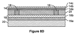
図7は、干渉変調器の製造プロセス80を示す流れ図の一例を示し、図8Aから図8Eは、このような製造プロセス80の対応する段階断面概略図の例を示す。いくつかの実施形態では、製造プロセス80は、図7に示されていない他のブロックに加えて、例えば図1および図6に示される概略的なタイプの干渉変調器を製造するために実施され得る。図1、図6、および図7を参照すると、プロセス80はブロック82で開始し、基板20の上に光学スタック16を形成する。図8Aは、基板20の上に形成されたこのような光学スタック16を示す。基板20は、ガラスまたはプラスチックなどの透明基板とすることができ、可撓性であってもよいし、比較的剛性で屈曲しなく(unbending)てもよく、光学スタック16の効率的な形成を容易にするために前の準備プロセス例えば洗浄を受けていてもよい。上記で説明したように、光学スタック16は、導電性で、部分的に透明かつ部分的に反射性とすることができ、例えば透明基板20上に所望の特性を有する一つまたは複数の層を堆積させることによって製作され得る。図8Aでは、光学スタック16は、副層16aおよび16bを有する多層構造を含むが、いくつかの他の実施形態では、より多くまたはより少ない副層が含まれ得る。いくつかの実施形態では、副層16a、16bのうちの一方は、一体化した導体/吸収体の副層16aなどの光学的吸収性特性と導電性特性の両方を有するように構成され得る。さらに、副層16a、16bのうちの一つまたは複数は、平行ストリップにパターニング可能であり、ディスプレイデバイス内に行電極を形成することができる。このようなパターニングは、マスキングプロセスおよびエッチングプロセスまたは当技術分野で知られている別の適切なプロセスによって実行され得る。いくつかの実施形態では、一つまたは複数の金属層(例えば、一つまたは複数の反射層および/または導電層)の上に堆積された副層16bなどの、副層16a、16bのうちの一方は、絶縁層であっても、または誘電体層であってもよい。さらに、光学スタック16は、ディスプレイの行を形成する個別の平行ストリップにパターニングされ得る。
FIG. 7 shows an example of a flow diagram illustrating an interferometric
プロセス80は、ブロック84に進み、犠牲層25が光学スタック16の上に形成される。犠牲層25は、後で、キャビティ19を形成するために除去され(例えばブロック90で)、したがって犠牲層25は、図1に示される得られる干渉変調器12内に示されていない。図8Bは、光学スタック16の上に形成された犠牲層25を含む部分的に製作されたデバイスを示す。光学スタック16の上の犠牲層25の形成は、続く除去の後で、所望の設計寸法を有するギャップまたはキャビティ19(図1および8Eも参照されたい)を形成するように選択された厚さをした、モリブデン(Mo)またはアモルファスシリコン(a−Si)などの二フッ化キセノン(XeF2)エッチング可能な材料の堆積を含むことができる。犠牲材料の堆積は、物理的気相成長(PVD、例えばスパッタリング)、プラズマ化学気相成長(PECVD)、熱化学気相成長(熱CVD)、またはスピンコーティングなどの堆積技法を使用して実行可能である。
プロセス80は、ブロック86に進み、支持構造例えば図1、図6、および図8Cに示される支柱18が形成される。支柱18の形成は、犠牲層25をパターニングして支持構造開口を形成するステップ、次にPVD、PECVD、熱CVD、またはスピンコーティングなどの堆積方法を使用して開口の内部に材料(例えば、ポリマーまたは無機材料例えば、酸化シリコン)を堆積させて支柱18を形成するステップを含むことができる。いくつかの実施形態では、犠牲層に形成された支持構造開口は、犠牲層25と光学スタック16の両方を貫通して、下にある基板20に至ることができ、したがって図6Aに示されるように、支柱18の下端は基板20と接触する。あるいは、図8Cに示されるように、犠牲層25に形成された開口は犠牲層25を貫通することはできるが、光学スタック16を貫通することはできない。例えば、図8Eは、支持支柱18の下端が光学スタック16の上側表面と接触することを示す。支柱18または他の支持構造は、犠牲層25の上に支持構造材料の層を堆積させ、犠牲層25内の開口から離れて位置する支持構造材料の一部分をパターニングすることによって、形成され得る。支持構造は、図8Cに示されるように開口の内部に位置され得るが、少なくとも一部は、犠牲層25の一部分の上に延びることもできる。前述のように、犠牲層25および/または支持支柱18のパターニングは、パターニングプロセスおよびエッチングプロセスによって実行可能であるが、代替エッチング方法によっても実行可能である。
プロセス80は、ブロック88に進み、図1、図6、および図8Dに示されている可動反射層14などの可動反射層または膜の形成が行われる。可動反射層14は、一つまたは複数のパターニングステップ、マスキングステップ、および/またはエッチングステップに加えて、一つまたは複数の堆積ステップ例えば反射層(例えば、アルミニウム、アルミニウム合金)の堆積を用いることによって形成され得る。可動反射層14は、電導性とすることができ、導電層と呼ばれ得る。いくつかの実施形態では、可動反射層14は、図8Dに示される複数の副層14a、14b、14cを含むことができる。いくつかの実施形態では、副層14a、14cなどの副層のうちの一つまたは複数は、光学的特性のために選択された非常に反射性の高い副層を含むことができ、別の副層14bは、その機械的特性ために選択された機械的な副層を含むことができる。犠牲層25はまだ、ブロック88で形成された部分的に製作された干渉変調器内に存在するので、可動反射層14は、典型的には、この段階では可動ではない。犠牲層25を含む部分的に製作されたIMODは、本明細書において「解放されていない(unreleased)」IMODと呼ばれることもある。図1に関連して上述したように、可動反射層14は、ディスプレイの列を形成する個別の平行ストリップにパターニングされ得る。
プロセス80は、ブロック90に進み、キャビティ例えば図1、図6、および図8Eに示されるキャビティ19が形成される。キャビティ19は、犠牲材料25(ブロック84で堆積された)をエッチング液に浸すことによって形成され得る。例えば、MoまたはアモルファスSiなどのエッチング可能な犠牲材料は、ケミカルドライエッチングによって、例えば、固体XeF2由来の蒸気などのガスまたは蒸気状のエッチング液に犠牲層25を、所望量の材料を除去するのに有効なある期間浸すことによって、除去可能であり、典型的には、キャビティ19を取り囲む構造に対して選択的に除去される。他のエッチング方法例えばウェットエッチングおよび/またはプラズマエッチングも使用可能である。犠牲層25がブロック90で除去されるので、可動反射層14は、典型的には、この段階の後で可動である。犠牲材料25の除去後、得られる完全にまたは部分的に製作されたIMODは、本明細書において、「解放」IMODと呼ばれることがある。
The
図9は、複数のコモンライン112、114、および116、ならびに複数のセグメントライン122、124、および126を含むディスプレイ要素102の配列100の一例を概略的に示す。いくつかの実施形態では、ディスプレイ要素102は、干渉変調器を含むことができる。複数のセグメント電極またはセグメントライン122、124、および126、ならびに複数のコモン電極またはコモンライン112、114、および116は、各ディスプレイ要素102がセグメント電極122、124、および126、ならびにコモン電極112、114、および116と電気通信するとき、ディスプレイ要素102をアドレス指定するのに使用され得る。セグメントドライバ回路104は、各セグメント電極122、124、および126に所望の電圧波形を印加するように構成され、コモンドライバ回路106は、各コモン電極112、114、および116に所望の電圧波形を印加するように構成される。いくつかの実施形態では、例えばセグメント電極124aおよび122aなどの電極のいくつかは、同一の電圧波形が各セグメント電極に同時に印加され得るように、互いに電気通信され得る。
FIG. 9 schematically illustrates an example of an
依然として図9に関し、ディスプレイ100がカラーディスプレイまたはモノクログレースケールディスプレイを含む実施形態では、個別の電気機械的要素102は、より大きな画素の副画素を含むことができ、その画素はいくつかの副画素を含む。配列が複数の干渉変調器を含むカラーディスプレイを含む実施形態では、様々な色が、所与のコモンラインに沿った実質的に全てのディスプレイ要素が同一の色を表示するように構成されたディスプレイ要素を含むように、コモンラインに沿って整列され得る。カラーディスプレイの特定の実施形態は、赤、緑、および青の副画素の交互ラインを含む。例えば、ライン112は、赤の干渉変調器のラインに対応することができ、ライン114は、緑の干渉変調器のラインに対応することができ、ライン116は、青の干渉変調器のラインに対応することができる。一実施形態では、干渉変調器102の各3×3配列は、画素130a−130dなどの画素を形成する。セグメント電極の二つが互いにショートしている例示の実施形態では、このような3×3画素は、64の異なる色(6−ビット色深度)を表示することができるが、それは、各画素における3つの共通カラー副画素の各セットが4つの異なる状態に配置され得るからである。この配置をモノクログレースケールモードで使用するとき、各色に対する3つの画素セットの状態が同一に作られ、その場合は、各画素が4つの異なるグレーレベル強度をとることができる。これは単に一例であり、全体の画素数または解像度を犠牲にして、干渉変調器のより大きな群がより大きなカラー範囲を有する画素を形成するために使用され得ることが認められよう。
Still referring to FIG. 9, in embodiments where the
[マルチラインアドレッシングモード]
特定のディスプレイでは、ディスプレイ要素にデータを書き込むのに必要な時間は、ディスプレイが書き込まれ得る全体的なレートに制限される。各コモンラインが別個にアドレス指定される場合、各ラインに必要な書き込み時間は、全体的なフレーム書き込み時間を決定する。特定の実施形態では、ディスプレイの増加されたリフレッシュレートまたはフレームレートが所望であり得、また、ユーザへの良好な外観のためのディスプレイの解像度または色の範囲よりもより重要であり得る。特定の実施形態では、幅広い色の範囲とともに高解像度の画像を提示することができるドライバ回路およびディスプレイ配列が、配列のコモンラインをストローブする種々の異なる「モード」で利用され得る。これらのモードは、解像度および色の範囲の一方または両方を減少するように設計され得、代わりに、同時に配列のマルチラインをストローブすることにより、ディスプレイのポテンシャルリフレッシュレートを増大させ、および/または電力消費を低下させる。これらのモードは、以下でさらに説明され、本明細書では、ディスプレイコントローラ操作の「マルチラインアドレッシングモード」と呼ばれる。まず、これらのモードの操作が説明され、モード制御の新規な方法が続く。
[Multi-line addressing mode]
For certain displays, the time required to write data to the display element is limited to the overall rate at which the display can be written. If each common line is addressed separately, the write time required for each line determines the overall frame write time. In certain embodiments, an increased refresh rate or frame rate of the display may be desired and may be more important than the resolution or color range of the display for a good appearance to the user. In certain embodiments, driver circuits and display arrays that can present high resolution images with a wide range of colors can be utilized in a variety of different “modes” that strobe the common lines of the array. These modes can be designed to reduce one or both of resolution and color range, instead increasing the potential refresh rate of the display by strobing multiple lines of the array at the same time and / or power Reduce consumption. These modes are further described below and are referred to herein as “multiline addressing modes” of display controller operation. First, the operation of these modes is described, followed by a new method of mode control.
特定の実施形態では、解像度は、同一の色のディスプレイ要素に対応するコモンラインに同一の波形を同時に印加することによって、効果的に低減され得る。例えば、書き込み波形が同時に赤のコモンライン112aおよび112bに印加されて、それらのコモンラインをアドレス指定する場合、コモンライン112aに沿って干渉変調器に書き込まれるデータパターンは、コモンライン112bに沿って干渉変調器に書き込まれるデータパターンと同一となる。書き込み波形が同時に緑のコモンライン114aおよび114bに、次いで青のコモンライン116aおよび116bに印加される場合、画素130aに書き込まれるデータパターンは、画素130bに書き込まれるデータパターンと同一となり、画素130aに画素130bと同一の色が表示される。用語「同時に(simultaneously)」が、簡潔さの目的で本議論を通じて使用されているが、電圧波形は完全に同時に動く必要はない。図5Bに関連して上述したように、書き込み波形は、ディスプレイ要素の電位差が適切なセグメント電圧が与えられたそのディスプレイ要素に書き込まれているデータを結果としてもたらすために十分である間のオーバードライブまたはアドレス電位を含むことができる。コモンラインに印加された書き込み波形のオーバードライブまたはアドレス電位と、全てのアドレス指定されたコモンライン上のディスプレイ要素の作動が生じるセグメントラインに印加されたデータ信号との間に十分なオーバーラップがある限り、書き込み波形とデータ信号とは、同時に印加されると考えられている。
In certain embodiments, resolution can be effectively reduced by simultaneously applying the same waveform to common lines corresponding to display elements of the same color. For example, if a write waveform is simultaneously applied to the red
各コモンラインが個別にアドレス指定される書き込みプロセスと比較すると、データは、低下された解像度を犠牲にして、画素130aおよび130bに別個のデータを書き込むのにかかる時間のわずか半分の時間で、画素130aおよび130bに書き込まれている。このライン乗算プロセス(line multiplying process)がディスプレイにおけるコモンラインの残り部分に適用される場合、フレーム書き込み時間は大幅に低減される。
Compared to a writing process in which each common line is individually addressed, the data is only half as long as it takes to write separate data to the
図10は、ライン乗算の使用を介して全体のフレーム書き込み時間を低減するフレーム書き込みプロセス200を示す流れ図である。この特定のフレーム書き込みプロセスは、完全なフレーム書き込みの一部のみを表すことができ、また、完全なフレーム書き込みの初め、中間、または終わりを含む完全なフレーム書き込みの間の任意の時間に生じることができる。従って、画像データは既に、フレーム内の一つまたは複数のコモンラインに書き込まれている。ブロック202では、同時にアドレス指定されるコモンラインの対または群が特定される。
FIG. 10 is a flow diagram illustrating a
ブロック204では、複数のデータ信号がセグメントラインに沿って印加される。同時に、ブロック206では、第一の書き込み波形が、波形をアドレス指定する配列における少なくとも二つのコモンラインに、同時に印加される。このような書き込み波形は、図5Bに関して上述したように、例えば、アドレス指定されているコモンラインへの適切な正または負のオーバードライブまたはアドレス電位を含むことができる。保持電圧は、アドレス指定されていない多数のコモンラインに同時に印加されることができ、リセット電圧は、コモンラインをアドレス指定する前に、コモンラインに印加されることができる。書き込み波形が、アドレス指定されるコモンラインの対または群に沿って印加されるとき、セグメントラインに沿った適切に選択されたデータ信号の印加は、アドレス指定されていないコモンラインに沿ったディスプレイ要素の予想外の作動または予想外の解放をもたらさない。
At
図10の流れ図は、ブロック206の前に生じるブロック204を示すが、所望の作動は、書き込み波形と複数のデータ信号との間に十分なオーバーラップがある限り生じ、全ての電気機械デバイスに、印加されたデータ信号に応じて作動または解放するための十分な時間を許容する。フレーム書き込み時間は故に、ブロック206の書き込み波形とブロック204のデータ信号との間のオーバーラップを最大化することによって低減され得、ブロック204および206は、信号の印加の間にオーバーラップがある限り、何れの順序でも生じ得る。
The flow diagram of FIG. 10 shows block 204 occurring before
ブロック208では、コモンラインの任意の追加の対または群が同時にアドレス指定されるかどうかについての決定がなされる。そうだとしたら、プロセスはブロック202に戻り、同時にアドレス指定するコモンラインの適切な対または群を選択する。そうでないとしたら、プロセスは、全ての必要なコモンラインがアドレス指定されている場合のフレーム書き込みプロセスの終端を含むか、または特定のコモンラインの個別のアドレス指定を含み得るさらなるブロックに移動する。加えて、コモンラインの対または群の同時アドレス指定は、書き込まれるデータの性質に応じて、コモンラインの個別のアドレス指定に組み入れられ得る。例えば、ディスプレイに書き込まれる画像データの一部が、テキストまたは別の静止画像を含み、データの別の部分が、低い解像度で表示され得、テキストまたは静止画像のセクション間に垂直に位置しているビデオを含む場合、ビデオ上部に位置するディスプレイの一部は、それらのコモンラインを個別にアドレス指定することによって書き込まれることができ、ビデオを含むディスプレイの一部は、ライン乗算書き込みプロセスを利用することによって低解像度で書き込まれることができ、書き込みプロセスは、ビデオ下部に位置するディスプレイの一部に対するディスプレイのコモンラインの個別のアドレス指定に戻ることができる。
At
上述のライン乗算の特定の方法は、有利なことに、隣接する画素におけるコモンラインに同一の書き込み波形を印加するが、コモンラインの他の対は他の実行で同時にアドレス指定され得る。さらに、たとえライン乗算方法が、書き込み波形を隣接する画素におけるコモンラインに同時に印加するのに使用されるとしても、画素の所与の対または群における全てのラインは、画素の他の群におけるラインに書き込む前に書き込まれる必要はない。特に、特定の実施形態では、別の色のコモンラインのアドレス指定の前に、同一色のコモンラインの多数の対または群をアドレス指定することが有利であり得る。例えば、赤のコモンライン112aおよび112bは、同時にアドレス指定され得、赤のコモンライン112cおよび112dを同時にアドレス指定する後続の書き込みプロセスが続く。異なる電圧波形は、異なる色のディスプレイ要素のコモンラインをアドレス指定するために使用され得るため、別の色のコモンラインのアドレス指定の前に、コモンラインの多数の対または群に対する特定の色に適している書き込み波形を利用することが有利であり得る。特定の実施形態では、所与の色のコモンラインのかなり多数の対または群が、別の色のコモンラインのアドレス指定の前に、連続してアドレス指定され得る。例えば、特定の実施形態では、所与の色のコモンラインの5つの対または群が、別の色のコモンラインがアドレス指定される前にアドレス指定され得るが、同様に、より多くのまたはより少ない数の対または群もまた使用され得る。
The particular method of line multiplication described above advantageously applies the same write waveform to the common lines in adjacent pixels, but other pairs of common lines can be addressed simultaneously in other implementations. Furthermore, even if the line multiplication method is used to apply the write waveform to the common lines in adjacent pixels at the same time, all lines in a given pair or group of pixels are lines in other groups of pixels. It need not be written before writing to. In particular, in certain embodiments, it may be advantageous to address multiple pairs or groups of common lines of the same color before addressing common lines of another color. For example, red
加えて、実質的に同一の波形の二つのコモンラインへの同時印加が本明細書で説明されているが、リフレッシュレートまたはフレーム書き込みのさらなる増加、あるいは電力使用の低減が、実質的に同一の波形を二つ以上のコモンラインに同時印加することによって達成され得る。 In addition, although the simultaneous application of substantially the same waveform to two common lines is described herein, further increases in refresh rate or frame writing, or reduction in power usage is substantially the same. This can be achieved by simultaneously applying a waveform to two or more common lines.
ディスプレイにおいてデータを更新するいくつかの方法では、特定のディスプレイ要素への電荷蓄積は、コモンラインに印加される書き込み波形の極性を変更することによって低減され得る。フレーム反転(frame inversion)と呼ばれ得る一実施形態では、所与のフレームは、特定の極性の書き込み波形を用いて完全にアドレス指定され、後続のフレームは、反対の極性の書き込み波形を用いて完全にアドレス指定される。さらなる実施形態では、しかしながら、書き込み波形の極性は、単一のフレーム書き込みの間に変更され得る。ライン反転(line inversion)と呼ばれ得る特定の実施形態では、書き込みの極性は、各ラインのアドレス指定の後に変更され得、特定のラインをアドレス指定するのに使用される極性は、後続のフレームで変化され得る。ディスプレイが実質的に直線的に更新されている場合、これは、反対の極性を有する書き込み電圧によってアドレス指定されている隣接ラインをもたらし得る。従って、特定の実施形態では、例えば、負の極性を有するスキップされた赤のコモンラインに書き込む前に、いくつかの数のコモンラインに対する正の極性を有する他のすべての赤のコモンラインに書き込むために、所与の極性を有する所与の書き込み波形を利用することが有利であり得る。 In some methods of updating data in the display, charge accumulation on a particular display element can be reduced by changing the polarity of the write waveform applied to the common line. In one embodiment, which can be referred to as frame inversion, a given frame is fully addressed with a write waveform of a particular polarity and subsequent frames are written with a write waveform of the opposite polarity. Fully addressed. In further embodiments, however, the polarity of the write waveform can be changed during a single frame write. In a particular embodiment, which can be referred to as line inversion, the polarity of the write can be changed after addressing each line, and the polarity used to address a particular line can be changed in subsequent frames. Can be changed. If the display is being updated substantially linearly, this can result in adjacent lines being addressed by a write voltage having the opposite polarity. Thus, in certain embodiments, for example, writing to all other red common lines having a positive polarity for some number of common lines before writing to a skipped red common line having a negative polarity. For this reason, it may be advantageous to utilize a given write waveform having a given polarity.
フレーム内の極性反転は、ライン乗算が同様に使用される書き込みプロセスに適用され得る。一実施形態では、赤のライン112cおよび112dは、所与のフレーム書き込み内の赤のライン112aおよび112bをアドレス指定するのに使用されるのと反対の極性を用いてアドレス指定され得る。所与の極性を有する書き込み波形が多数の後続のアドレス指定操作に対して使用される上述の一つのような実施形態では、赤のライン112aおよび112bは、第一極性を用いてアドレス指定され得、赤のライン112cおよび112dはスキップされ得、一方で、赤のラインのいくつかの数の追加の対または群が、第一極性を用いて書き込まれる。いくつかの数の対または群が第一極性を用いてアドレス指定された後、赤のライン112cおよび112dは、反対の極性を用いてアドレス指定され得る。
Polarity reversal within a frame can be applied to a writing process where line multiplication is used as well. In one embodiment,
極性反転が利用される場合、第一極性を用いた一色の特定の数のラインのアドレス指定の後に、反対の極性を用いた同一色における特定の数のラインのアドレス指定が続く必要はない。他の実施形態では、正の赤の書き込みプロセスの後に、例えば、負の青の書き込みプロセス、または正の緑の書き込みプロセスが続くことがある。 If polarity reversal is utilized, the addressing of a specific number of lines of one color using the first polarity need not be followed by the addressing of a specific number of lines in the same color using the opposite polarity. In other embodiments, a positive red writing process may be followed by, for example, a negative blue writing process or a positive green writing process.
別の実施形態では、カラーディスプレイは、利用可能な色の範囲を低減するモノクロモードまたは他のモードで駆動され得る。この方法でディスプレイを更新するプロセスは、ディスプレイの解像度を低下させることなくディスプレイをリフレッシュするために必要な時間を低減することができる。一実施形態では、ディスプレイは、隣接するコモンラインに書き込み波形を同時に印加することによって、モノクロ方法で駆動され得る。例えば、図9に示すようなRGBディスプレイでは、画素130aを介して広がる三つの隣接するコモンライン112a、114aおよび116aは、これらの三つのコモンラインのそれぞれに書き込み波形を印加することによって、同時にアドレス指定される。特定の実施形態では、アドレス指定されているコモンラインの色に特有の書き込み電圧が、これらの三つのコモンラインのそれぞれで使用され得、他の実施形態では、コモンライン内の様々な色のディスプレイ要素のそれぞれをアドレス指定するのに適するように選択された単一の書き込み波形が使用され得る。適切な書き込み波形が選択される場合、同一の副画素がコモンラインのそれぞれで作動され、画素130aは、四つの電位遮蔽(potential shade)を有するグレースケール画素として駆動され得る。
In another embodiment, the color display may be driven in monochrome mode or other modes that reduce the range of available colors. The process of updating the display in this manner can reduce the time required to refresh the display without reducing the display resolution. In one embodiment, the display can be driven in a monochrome manner by simultaneously applying a write waveform to adjacent common lines. For example, in an RGB display as shown in FIG. 9, three adjacent
他の実施形態では、可能な色の範囲は、そのディスプレイをモノクロディスプレイに低減することなくポテンシャルリフレッシュレートを増加させるように低減され得る。例えば、三つの異なる色のディスプレイ要素を有するディスプレイでは、所与の画素における二つの色は同時にアドレス指定され得、一方、他の色は独立してアドレス指定され、モノクロよりロバストであるが全ての三つの色が独立してアドレス指定される場合に可能なものよりはロバストでない色の範囲を生み出す。代替実施形態では、一つまたは複数の色はアドレス指定されずに残され得る。 In other embodiments, the range of possible colors can be reduced to increase the potential refresh rate without reducing the display to a monochrome display. For example, in a display with three different color display elements, the two colors in a given pixel can be addressed simultaneously, while the other colors are addressed independently and are more robust than monochrome but all Produces a range of colors that is less robust than is possible when the three colors are addressed independently. In alternative embodiments, one or more colors may be left unaddressed.
図11は、ディスプレイの少なくとも一部へのモノクロモードの使用を介したディスプレイの全体のフレーム書き込み時間を低減するためのフレーム書き込みプロセス300を示す流れ図である。フレーム書き込みプロセス200に関して上述したように、このプロセスは、全体のフレーム書き込み、または、例えばフレーム書き込みの初め、中間、または終わりのみなどのフレーム書き込みの一部の間のみに使用され得る。従って、画像データは、プロセス300の前および/または後にラインに書き込まれ得る。
FIG. 11 is a flow diagram illustrating a
ブロック302では、アドレス指定されるコモンラインの群が選択される。RGBディスプレイなどの、三つの異なる色のディスプレイ要素を有するディスプレイでは、選択された色の群は、所与の画素を介して広がる各色の隣接するコモンラインを含むことができる。ブロック304では、データ信号は、複数のセグメントラインに同時に印加される。ブロック306では、書き込み波形は、選択されたそれぞれのコモンラインに同時に印加される。上述のように、このプロセスは、異なる色のディスプレイ要素の同時アドレス指定を含むため、コモンラインの色に特有の異なる書き込み波形がアドレス指定されるそれぞれの色に対して使用され得るが、アドレス指定される全ての色に適する単一の書き込み波形もまた、代替実施形態で使用され得る。ブロック304と306との間の十分なオーバーラップを所与として、データ信号は、アドレス指定されたコモンラインへの画像データの書き込みをもたらす。
At
ブロック308では、次のライン書き込みを多数のコモンラインを同時にアドレス指定するモノクロライン書き込みとするかどうかについての決定がなされる。もしそうなら、そのプロセスはブロック302に戻り、同時にアドレス指定されるコモンラインを選択する。もしそうでないなら、そのプロセスは、単一のコモンラインのみをアドレス指定するカラーライン書き込みを含む他の段階に移動するか、または、フレーム書き込みは完了し得る。
At
さらなる実施形態では、上述のタイプのライン乗算は、表示される特定の情報に応じて、ディスプレイの特定のセクションのみで使用され得る。ディスプレイデバイスの多くの実施形態は、データの多くの部分が異なるコモンライン上で同一(またはほぼ同一)であるように、頻繁に情報を表示する。例えば、電子書籍または他のテキストディスプレイデバイス上のテキストのライン間のスペースは、白一色または別の色であり得る。多数のコモンラインに沿って画素に書き込まれるデータが多数のコモンラインに対して一定のままであるこのような実施形態では、同一のセグメントデータを共有するコラムラインが同時に書き込まれるか、またはアドレス指定され得る。書き込み波形がこれらのコモンラインのそれぞれに同時に印加されるとき、セグメントライン上のデータは、アドレス指定されているコモンラインのそれぞれに書き込まれる。フレーム書き込みを完了するのに必要な全体の時間を低減することに加えて、追加の電力がセグメント電圧スイッチを最小化することによって削減され得る。 In further embodiments, the types of line multiplication described above may be used only in certain sections of the display, depending on the particular information displayed. Many embodiments of display devices frequently display information so that many portions of the data are the same (or nearly the same) on different common lines. For example, the space between lines of text on an electronic book or other text display device may be white or another color. In such an embodiment where the data written to the pixels along multiple common lines remains constant for multiple common lines, column lines sharing the same segment data are simultaneously written or addressed. Can be done. When a write waveform is applied simultaneously to each of these common lines, the data on the segment line is written to each of the addressed common lines. In addition to reducing the overall time required to complete a frame write, additional power can be reduced by minimizing the segment voltage switch.
上記の実施形態は3×3画素の使用について説明してきたが、任意の所望のサイズおよび形状の画素およびディスプレイ要素が本明細書に記載の方法およびデバイスと併せて使用され得ることが理解されよう。例えば、画素が三つ以上のセグメントラインを覆うか、またはセグメントラインのそれぞれが互いに独立している場合、増大された色またはグレースケールの範囲が提供され得る。 While the above embodiments have described the use of 3 × 3 pixels, it will be understood that any desired size and shape of pixels and display elements can be used in conjunction with the methods and devices described herein. . For example, if a pixel covers more than two segment lines, or each of the segment lines is independent of each other, an increased color or gray scale range can be provided.
上記の駆動スキームおよび他の技術は、ディスプレイのリフレッシュレートの増加と併せて使用される必要はない。例えば、上記の方法の多くは、電力消費の顕著な低減をもたらすことができ、ディスプレイによって利用される電力を低減するために適用され得る。電力使用の低減は、電力使用の低減がより長い電池寿命をもたらすことができる電池式または他の携帯デバイスに特定の関心をもたらし得る。 The drive schemes and other techniques described above need not be used in conjunction with increasing the display refresh rate. For example, many of the methods described above can result in a significant reduction in power consumption and can be applied to reduce the power utilized by the display. Reduced power usage may bring particular interest to battery powered or other portable devices where reduced power usage can result in longer battery life.
時として、ビデオまたは他のアニメーションのディスプレイなどにおいて、高いリフレッシュレートまたはフレームレートは、ディスプレイの解像度よりも、より良好な外観に対してより重要であり得る。例えば、低解像度プレビュー画像が示され、次いで最大解像度画像で置き換えられ得るか、または、ズーミングアニメーションを含むGUIが低解像度でズーミングアニメーションを表示し、次いでズーミングアニメーションが完了するとき高解像度に戻ることがある。いくつかの実施形態では、解像度は、多数のコモンラインに同一の電圧波形を同時に印加することによって、高いフレームレートのための犠牲となる。 Sometimes, such as in video or other animated displays, a high refresh rate or frame rate may be more important for a better appearance than the resolution of the display. For example, a low resolution preview image may be shown and then replaced with a full resolution image, or a GUI that includes a zooming animation may display a zooming animation at a low resolution and then return to a high resolution when the zooming animation is complete. is there. In some embodiments, resolution is sacrificed for high frame rates by simultaneously applying the same voltage waveform to multiple common lines.
さらなる実施形態では、ディスプレイの解像度がソースデータの解像度より大きいとき、多数のディスプレイ要素への同一のデータの同時書き込みは、結果として生じる画像にネガティブな視覚効果を有することなくフレーム書き込み時間を低減することができるが、それは、同一のデータが既に特定の隣接するディスプレイ要素に書き込まれているからである。ビデオデータは例えば、ビデオデータ自身よりも高い解像度を有するディスプレイで頻繁にみられるが、多くの他のタイプの画像ソースデータは、その画像データが書き込まれるディスプレイよりも低い解像度であり得る。多数のラインに同一のデータを書き込むためのライン乗算の使用は、有利なことに、フレーム書き込み時間を低減し、最終的なディスプレイ画像に有害な影響なく可能なリフレッシュレートを増加させる。 In a further embodiment, when the resolution of the display is greater than the resolution of the source data, simultaneous writing of the same data to multiple display elements reduces the frame writing time without having a negative visual effect on the resulting image. This is because the same data has already been written to a particular adjacent display element. For example, video data is often found on a display having a higher resolution than the video data itself, but many other types of image source data may be at a lower resolution than the display on which the image data is written. The use of line multiplication to write the same data to multiple lines advantageously reduces the frame writing time and increases the possible refresh rate without detrimental effects on the final display image.
いくつかの実施形態の一態様では、これらの「マルチラインアドレッシング」モードは、ホストソフトウェアの制御下のディスプレイコントローラによって入力および終了され得る。ホストソフトウェアは、ホストソフトウェアが表示を欲するデータの性質に関する大量の情報を有する。この情報に基づき、ホストはディスプレイコントローラを、ディスプレイデータの性質に対して最適なモードにすることができる。例えば、ホストソフトウェアは、ディスプレイが各ラインを別個に更新する必要がある場合、ディスプレイのための更新レートよりも速いフレームレートを有するH.264ビデオストリームをそれが解読することを理解することができる。この場合、ホストはディスプレイコントローラを(例えば、最大ディスプレイ解像度の半分で)マルチラインアドレッシングモードにすることができ、故に、ディスプレイはフレームレートについていくことができる。このモード制御は、例えば、ホストによって書き込まれ得るディスプレイコントローラにおけるレジスタによって提供され得、記憶されたレジスタ値は、その動作モードを決定するために、コントローラによって読まれる。 In one aspect of some embodiments, these “multiline addressing” modes may be entered and terminated by a display controller under the control of host software. The host software has a large amount of information regarding the nature of the data that the host software wants to display. Based on this information, the host can put the display controller into a mode that is optimal for the nature of the display data. For example, if the display software needs to update each line separately, the H.264 software has a frame rate that is faster than the update rate for the display. It can be seen that it decodes the H.264 video stream. In this case, the host can put the display controller into a multi-line addressing mode (eg, at half the maximum display resolution) and thus the display can keep up with the frame rate. This mode control can be provided, for example, by a register in the display controller that can be written by the host, and the stored register value is read by the controller to determine its operating mode.
別の例として、ホストは、表示される画像が変化しているかどうかについて決定することができる。画像が変化している(例えば、ビデオが表示されている)場合、ホストは、より高いフレームレートに対応するマルチラインアドレッシングモードを選択することができる。画像または画像の一部が変化したかどうかを決定するため、ホストは一つの画像を後続の画像と比べることができる。画像が変化したかどうかの決定は、第一画像全体(またはその一部)を第二画像全体(またはその一部)と比較することを含むことができる。いくつかの実施形態では、ホストは代わりに、画像データを作動するアルゴリズムの出力を比較することができる。例えば、ホストは、第一画像(またはその一部)に対する周期的冗長検査(CRC)値を第二画像(またはその一部)に対するCRC値と比較することができる。 As another example, the host can determine whether the displayed image has changed. If the image is changing (eg, video is being displayed), the host can select a multi-line addressing mode that corresponds to a higher frame rate. To determine if an image or part of an image has changed, the host can compare one image with subsequent images. Determining whether the image has changed may include comparing the entire first image (or a portion thereof) with the entire second image (or a portion thereof). In some embodiments, the host can instead compare the output of algorithms that operate on the image data. For example, the host can compare a cyclic redundancy check (CRC) value for a first image (or part thereof) with a CRC value for a second image (or part thereof).
別の例として、ホストは、QVGAデータ(320×240)をディスプレイに送ることができる。これは、ディスプレイの典型的な画素解像度と比較して非常に低解像度の画像データであるため、ホストは、ディスプレイコントローラを320×240解像度のマルチラインアドレッシングモード(例えば、元の解像度の四分の一)にすることができ、リフレッシュレートを増加し、および/または電力を節約する。 As another example, the host can send QVGA data (320 × 240) to the display. Since this is very low resolution image data compared to the typical pixel resolution of the display, the host can set the display controller to a 320 × 240 resolution multi-line addressing mode (eg, a quarter of the original resolution). 1) can increase the refresh rate and / or save power.
別の例は、急速なディスプレイ変化をもたらすズーミングのためのピンチなどのタッチスクリーン入力を受け取るホストプログラムである。ホストは、これらの入力を感じることができ、ディスプレイを低解像度にし、これらの更新の間にモードを素早く更新し、そして、ディスプレイデータがもはや素早く変化しないときはディスプレイコントローラを最大解像度モードに切り替える。いくつかの実施形態では、ホストは、それらに限定されないが、ポインティングデバイス(例えば、マウス、タッチパッド、ポインティングスティック、トラックボール、またはスタイラスなど)、加速度計、キーボード、ジャイロスコープ、音声コマンド、カメラ、または任意の他の触知性または非触知性のユーザ入力デバイスからの入力を含む他のユーザ入力に対応答して、マルチラインアドレッシングモードを自動で選択することができる。 Another example is a host program that receives touch screen input such as a pinch for zooming that results in rapid display changes. The host can feel these inputs, bring the display to a lower resolution, update the mode quickly between these updates, and switch the display controller to full resolution mode when the display data no longer changes quickly. In some embodiments, the host includes, but is not limited to, a pointing device (eg, mouse, touchpad, pointing stick, trackball, or stylus), accelerometer, keyboard, gyroscope, voice command, camera, Alternatively, the multi-line addressing mode can be automatically selected in response to other user input including input from any other tactile or non-tactile user input device.
場合によっては、これらのモードは、単一のフレームの書き込みの間に入力および終了され得る。ディスプレイコントローラにモードレジスタがある場合、これは各ラインストローブの間(または画素の各ラインの完了の間)にチェックされ得、故に多数のマルチラインアドレッシングモードは、フレームの一部に対して実施され得る。これは、画像データが同一ラインのかなりの領域を有する場合に有益であり得、そこで、これらの領域は、上述のマルチラインアドレッシングモードでアドレス指定され得るが、フレームの残りでは、一度にラインをストローブする。他の場合、コントローラは、このような変化がディスプレイの外観にひどい悪影響を及ぼすとき、モード変化が非常に素早く生じるのを防ぐように構成され得る。例えば、コントローラがモードを変化するように指示される場合、特定の数のラインまたはフレームがスイッチを作る前に電流モードを用いて書き込まれることを保証できる。 In some cases, these modes may be entered and terminated during the writing of a single frame. If the display controller has a mode register, this can be checked during each line strobe (or during the completion of each line of pixels), so multiple multi-line addressing modes are implemented for part of the frame. obtain. This can be beneficial when the image data has a significant area of the same line, where these areas can be addressed in the multiline addressing mode described above, but for the remainder of the frame, the lines are Strobe. In other cases, the controller may be configured to prevent mode changes from occurring very quickly when such changes severely affect the appearance of the display. For example, if the controller is instructed to change modes, it can be guaranteed that a certain number of lines or frames will be written using the current mode before making the switch.
ホストが例えばウェブブラウザを起動し、ユーザがウェブページにアクセスする場合、新しい画像を有するフレーム更新がまれに生じるため、ホストはディスプレイコントローラを最大解像度モードにセットすることができる。ビデオを有するフラッシュ(登録商標)ウィンドウが開かれる場合、マルチラインアドレッシングモードは、ウィンドウを含むディスプレイのそれらのラインに対してセットされ得る。これらのモードはまた、ビデオウィンドウの状況に基づいて、ホストによって選択され得る。例えば、ビデオが中断または停止される場合、最大解像度モードが使用され得る。モード選択がホストによってなされる一実施形態では、ホストは、ラインダブリングモードで無視されるフレームバッファにディスプレイデータを書き込むことを抑制することができる。この方法では、データをフレームバッファに書き込む際に消費されるエネルギーが節約され得る。 If the host launches a web browser, for example, and the user accesses a web page, the host can set the display controller to full resolution mode because frame updates with new images occur infrequently. When a flash window with video is opened, the multi-line addressing mode can be set for those lines of the display containing the window. These modes can also be selected by the host based on the status of the video window. For example, if the video is interrupted or stopped, the maximum resolution mode may be used. In one embodiment where the mode selection is made by the host, the host can suppress writing display data to a frame buffer that is ignored in line doubling mode. In this way, the energy consumed when writing data to the frame buffer can be saved.
いくつかの実施形態では、ホストおよび/またはコントローラは、いくつかのしきい値を超えて変化してきたラインのみを選択的に更新するために、どの画像のラインが変化したかについての情報を使用することができる。ビデオウィンドウディスプレイを例として用いると、ウィンドウが画像の一部分であり、画像の残りが変化しない場合、ウィンドウを含むラインのみが更新される。これは、ウィンドウを有するラインのみが更新されるように上述のマルチラインアドレッシングモードと結合されることができ、それらのラインはマルチラインアドレッシングモードで更新される。 In some embodiments, the host and / or controller uses information about which image lines have changed to selectively update only those lines that have changed beyond some threshold. can do. Using a video window display as an example, if the window is part of an image and the rest of the image does not change, only the line containing the window is updated. This can be combined with the multiline addressing mode described above so that only lines with windows are updated, and those lines are updated in multiline addressing mode.
図12は、マルチラインアドレッシングモードによりディスプレイを更新するための例示プロセス400を示す流れ図であり、そこで、マルチラインアドレッシングモードの選択は、表示されるデータに少なくとも一部基づく。ブロック402では、表示されるデータが得られる。ブロック404では、マルチラインアドレッシングモードが選択され、その選択は、表示されるデータに少なくとも一部基づく。マルチラインアドレッシングモードは、もしあれば、どのコモンラインが同時に同一データで書き込まれるかを決定する。例えば、上述のように、表示されるデータがビデオである場合、ディスプレイリフレッシュレートを増加させるマルチラインアドレッシングモードが選択され得る。例えば、いくつかの実施形態では、隣接する画素のコモンラインを同一のデータで書き込むマルチラインアドレッシングモードが選択され得、低下された解像度をもたらす。他の実施形態では、画素の同一ラインにおける異なる色の副画素に対応するコモンラインを同一データで書き込むマルチラインアドレッシングモードが選択され得、モノクロ色深度をもたらす。ブロック406では、ディスプレイが選択されたマルチラインアドレッシングモードに応じて更新される。
FIG. 12 is a flow diagram illustrating an
さらに図12に示される例に関して、マルチラインアドレッシングモードの選択は、表示されるデータに少なくとも一部基づく。例えば、いくつかの実施形態では、マルチラインアドレッシングモードの選択は、データ自身のフォーマット(例えば、画像、ビデオ、テキスト)に基づくことができる。マルチラインアドレッシングモードの選択はまた、表示されるデータ以外の何かに基づくこともできる。例えば、マルチラインアドレッシングモードの選択はまた、例えば電池残量またはユーザ入力によってもたらされる電力効率結果に一部基づくことができる。 Further with respect to the example shown in FIG. 12, the selection of the multi-line addressing mode is based at least in part on the displayed data. For example, in some embodiments, the selection of the multi-line addressing mode can be based on the data's own format (eg, image, video, text). The selection of the multi-line addressing mode can also be based on something other than the data being displayed. For example, the selection of the multi-line addressing mode can also be based in part on the power efficiency result provided by, for example, battery level or user input.
[ラインオーダーアドレッシングモード]
場合によっては、コモンラインをストローブする異なるモードは、ディスプレイの外観に影響を及ぼすが、フレーム書き込み時間または電力消費は大幅に変化させない。これらは本明細書では、「ラインオーダーアドレッシングモード」と呼ばれる。図13は、非線形の順序で更新されているディスプレイ要素の配列の一例を概略的に示す。図示されたストローブパターンは、不可視スキャン(invisible scan)と呼ばれることがある。このアドレッシングモードでは、ディスプレイ830のラインは、従来の順次的隣接ライン更新順序以外の順序で更新される。例えば、一実施形態では、ディスプレイ830のラインは、ランダムな順序で更新され得る。図示したように、タイムワン(Time one)1035では、ライン1036が更新される。タイムツー(Time two)1050では、ライン1038が更新される。ライン1036および1038は隣接していない。タイムスリー(Time three)1060では、ライン1046が更新される。この場合もやはり、ライン1040はライン1038と隣接していない。不可視スキャンモードにおけるライン更新の順序は、生成疑似乱数に基づいてダイナミックに決定される。代わりに、ラインに対する更新順序は、ランダムに見える一つまたは複数の所定のシーケンスに応じて決定され得る。図13における例は、直前または直後のライン更新と隣接していないライン更新を示すが、「不可視スキャン」効果を維持しつつ、いくつかのライン更新が直前または直後のライン更新と隣接していることが可能である。不可視スキャンモードは、特定の条件で視覚効果を届けるために使用され得る。例えば、不可視スキャンモードは、スライドショーにおける静止画像間のスイッチングの際に使用され得る。代わりに、不可視スキャンモードは、ホストを作動する異なるアプリケーションを表すウィンドウ間のスイッチングの際に使用され得る。前に注意したように、ホストまたはコントローラは、ディスプレイデータに関するデータにおけるフラッグ、ディスプレイデータの特性、またはホストのステータスに基づいて、不可視の更新モードを選択することができる。
[Line order addressing mode]
In some cases, different modes of strobing the common line affect the appearance of the display, but do not significantly change the frame writing time or power consumption. These are referred to herein as “line order addressing modes”. FIG. 13 schematically illustrates an example of an array of display elements that are updated in a non-linear order. The illustrated strobe pattern may be referred to as an invisible scan. In this addressing mode, the lines on the
図14は、ラインオーダーアドレッシングモードに応じてディスプレイを更新するための例示プロセスを示す流れ図であり、そこで、ラインオーダーアドレッシングモードの選択は、表示されるデータに少なくとも一部基づく。ブロック502では、表示されるデータが得られる。ブロック504では、ラインオーダーアドレッシングモードが選択され、その選択は、表示されるデータに少なくとも一部基づく。ラインオーダーアドレッシングモードは、コモンラインが表示されるデータで書き込まれる順序を決定する。例えば、表示されるデータがスライドショーにおける画像を含む上述のように、画像間に不可視スキャンを提供するラインオーダーアドレッシングモードが選択され得る。ブロック506では、ディスプレイは選択されたラインオーダーアドレッシングモードに応じて更新される。
FIG. 14 is a flow diagram illustrating an example process for updating a display in response to a line order addressing mode, where the selection of the line order addressing mode is based at least in part on the displayed data. At
[カラープロセッシングモード]
ホストが制御できる他のモードは、マルチラインアドレッシングまたはラインオーダーアドレッシングを含まないことがある。これらのディスプレイデバイスの多くの実施形態では、画像データの各画素は、三色のそれぞれを規定する特定データ値として規定される。ディスプレイのカラーパレットは、入ってくるデータのカラーパレットとは異なることがある。これらの場合、また同様に他の理由のために、ディスプレイコントローラは、各画素の元のデータを処理し、元の画像データの外観を正確に再生するディスプレイ配列に適している三つの画素明度を作ることができる。画像データの性質に応じて、このカラープロセッシングは実行される必要がないことがある。ホストが元のデータフォーマットの情報を有するため、それは多数の異なる「カラープロセッシング」モードでディスプレイコントローラを配置することができる。画像データが既にディスプレイに適合するフォーマットである場合、カラープロセッシングは止めることができ、電力および計算時間を省くことができる。
[Color processing mode]
Other modes that the host can control may not include multi-line addressing or line order addressing. In many embodiments of these display devices, each pixel of the image data is defined as a specific data value that defines each of the three colors. The color palette of the display may be different from the color palette of the incoming data. In these cases, and for other reasons as well, the display controller processes the original data for each pixel and produces three pixel brightness values that are suitable for display arrays that accurately reproduce the appearance of the original image data. Can be made. Depending on the nature of the image data, this color processing may not need to be performed. Since the host has information of the original data format, it can place the display controller in a number of different “color processing” modes. If the image data is already in a format that fits the display, color processing can be stopped and power and computation time can be saved.
図15は、カラープロセッシングモードに応じてディスプレイを更新するための例示プロセスを示す流れ図であり、そこで、カラープロセッシングモードの選択は、表示されるデータに少なくとも一部基づく。ブロック602では、表示されるデータが得られる。ブロック604では、カラープロセッシングモードが選択され、その選択は、表示されるデータに少なくとも一部基づく。カラープロセッシングモードは、表示されるデータ内の色情報が表示される前に処理されるかどうかを決定する。例えば、表示されるデータ内の色情報が処理されることなく表示可能である上述のように、色情報を処理しないカラープロセッシングモードが選択され得る。ブロック606では、ディスプレイが選択されたカラープロセッシングモードに応じて更新される。
FIG. 15 is a flow diagram illustrating an example process for updating a display in response to a color processing mode, where the selection of the color processing mode is based at least in part on the data being displayed. At
図16Aおよび図16Bは、複数の干渉変調器を含むディスプレイデバイスを示すシステムブロック図の例を示す。ディスプレイデバイス40は、例えば、セルラー式電話機または携帯電話機とすることができる。しかし、ディスプレイデバイス40の同じ構成要素またはそのわずかな変形形態も、テレビ、電子書籍リーダー、タブレット、および携帯型メディアプレーヤなどの種々のタイプのディスプレイデバイスを例示するものである。
16A and 16B show example system block diagrams illustrating a display device that includes multiple interferometric modulators. The
ディスプレイデバイス40は、筐体41と、ディスプレイ30と、アンテナ43と、スピーカ45と、入力デバイス48と、マイクロホン46とを含む。筐体41は、射出成形および真空成形を含むさまざまな製造プロセスのいずれかから形成され得る。さらに、筐体41は、プラスチック、金属、ガラス、ゴム、およびセラミック、またはこれらの組み合わせを含むがこれらに限定されないさまざまな材料のいずれかから作製され得る。筐体41は、異なる色をしたまたは異なるロゴ、画像、もしくは記号を含む他の着脱可能な一部分と交換され得る着脱可能な部分(図示せず)を含むことができる。
The
ディスプレイ30は、本明細書において説明する、双安定ディスプレイまたはアナログディスプレイを含む、さまざまなディスプレイのいずれかであってよい。ディスプレイ30はまた、プラズマ、EL、OLED、STN LCD、もしくはTFT LCDなどのフラットパネルディスプレイ、またはCRTもしくは他の管デバイスなどの非フラットパネルディスプレイを含むように構成され得る。さらに、ディスプレイ30は、本明細書において説明するように、干渉変調器ディスプレイを含むことができる。
ディスプレイデバイス40の構成要素は、図16Bに概略的に示されている。ディスプレイデバイス40は、筐体41を含み、その中に少なくとも部分的に納められた追加の構成要素を含むことができる。例えば、ディスプレイデバイス40は、トランシーバ47に結合されたアンテナ43を含むネットワークインタフェース27を含む。トランシーバ47は、プロセッサ21に接続され、プロセッサ21は、調整用ハードウェア(conditioning hardware)52に接続される。調整用ハードウェア52は、信号を調整する(例えば、信号をフィルタリングする)ように構成され得る。調整用ハードウェア52は、スピーカ45およびマイクロホン46に接続される。プロセッサ21は、入力デバイス48およびドライバコントローラ29にも接続される。ドライバコントローラ29は、フレームバッファ28および配列ドライバ22に結合され、配列ドライバ22は、ディスプレイ配列30に結合される。電源50は、特定のディスプレイデバイス40の設計によって必要とされるすべての構成要素に電力を供給することができる。
The components of
ネットワークインタフェース27は、アンテナ43とトランシーバ47とを含み、その結果、ディスプレイデバイス40は、ネットワークを介して一つまたは複数のデバイスと通信することができる。ネットワークインタフェース27は、例えばプロセッサ21のデータ処理要件を軽減するためにいくつかの処理能力も有することができる。アンテナ43は、信号を送信および受信することができる。いくつかの実施形態では、アンテナ43は、IEEE 16.11(a)、(b)、もしくは(g)を含むIEEE 16.11規格またはIEEE 802.11a、b、g、もしくはnを含むIEEE 802.11規格に従ってRF信号を送信および受信する。いくつかの他の実施形態では、アンテナ43は、ブルートゥース規格に従ってRF信号を送信および受信する。セルラー式電話の場合、アンテナ43は、符号分割多元接続(CDMA)、周波数分割多元接続(FDMA)、時分割多元接続(TDMA)、Global System for Mobile communications(GSM)、GSM/General Packet Radio Service(GPRS)、Enhanced Data GSM Environment(EDGE)、Terrestrial Trunked Radio(TETRA)、広帯域CDMA(W−CDMA)、Evolution Data Optimized(EV−DO)、1xEV−DO、EV−DO Rev A、EV−DO Rev B、High Speed Packet Access(HSPA)、High Speed Downlink Packet Access(HSDPA)、High Speed Uplink Packet Access(HSUPA)、Evolved High Speed Packet Access(HSPA+)、Long Term Evolution(LTE)、AMPS、または3G技術もしくは4G技術を利用するシステムなどのワイヤレスネットワーク内で通信するために使用される他の知られている信号を受信するように設計される。トランシーバ47は、アンテナ43から受信された信号を、これらがプロセッサ21によって受信され、さらに操作可能であるように前処理することができる。トランシーバ47はまた、プロセッサ21から受信された信号を、これらがアンテナ43を介してディスプレイデバイス40から送信可能であるように処理することができる。
The
いくつかの実施形態では、トランシーバ47は、受信機と交換され得る。さらに、ネットワークインタフェース27は、プロセッサ21に送られるべき画像データを保存または生成できる画像ソースと交換され得る。プロセッサ21は、ディスプレイデバイス40の全体的な動作を制御することができる。プロセッサ21は、ネットワークインタフェース27または画像ソースから圧縮画像データなどのデータを受信し、そのデータを処理して未加工の画像データを、または未加工の画像データに容易に処理されるフォーマットを生成する。プロセッサ21は、この処理されたデータをドライバコントローラ29に、または保存するためにフレームバッファ28に送ることができる。未加工のデータとは、典型的には、画像内の各場所における画像特性を識別する情報を指す。例えば、このような画像特性は、色、彩度、およびグレースケールレベルを含むことができる。
In some embodiments, the
プロセッサ21は、ディスプレイデバイス40の動作を制御するためにマイクロコントローラ、CPU、または論理演算装置を含むことができ、上記のディスプレイモード制御を実施するホストソフトウェアを実行することができる。調整用ハードウェア52は、信号をスピーカ45に送信するための、および信号をマイクロホン46から受信するための、増幅器とフィルタとを含んでもよい。調整用ハードウェア52は、ディスプレイデバイス40内の個別構成要素品であっても、あるいはプロセッサ21または他の構成要素内に組み込まれてもよい。
The
ドライバコントローラ29は、プロセッサ21によって生成された未加工の画像データを、プロセッサ21から直接またはフレームバッファ28から取得でき、配列ドライバ22への高速送信のために未加工の画像データを適切に再フォーマットすることができる。いくつかの実施形態では、ドライバコントローラ29は、ディスプレイ配列30全体にわたって走査に適した時間順序を有するように、未加工の画像データをラスターのようなフォーマットを有するデータフローに再フォーマットすることができる。次に、ドライバコントローラ29は、フォーマットした情報を配列ドライバ22に送る。LCDコントローラなどのドライバコントローラ29は、独立した集積回路(IC)としてシステムプロセッサ21を関連付けられることが多いが、このようなコントローラは多数の方法で実施され得る。例えば、コントローラは、ハードウェアとしてプロセッサ21に埋め込まれても、ソフトウェアとしてプロセッサ21に埋め込まれても、またはハードウェア内で配列ドライバ22と完全に一体化されてもよい。
The
配列ドライバ22は、フォーマットされた情報をドライバコントローラ29から受信でき、ディスプレイの画素のxy行列から来る、数百、場合によっては数千(またはそれ以上)のリード線に毎秒多数回印加される並列な1組の波形にビデオデータを再フォーマットすることができる。
The
いくつかの実施形態では、ドライバコントローラ29、配列ドライバ22、およびディスプレイ配列30は、本明細書において説明するディスプレイのタイプのいずれかに適している。例えば、ドライバコントローラ29は、従来のディスプレイコントローラまたは双安定ディスプレイコントローラ(例えばIMODコントローラ)とすることができる。さらに、配列ドライバ22は、従来のドライバまたは双安定ディスプレイドライバ(例えばIMODディスプレイドライバ)とすることができる。さらに、ディスプレイ配列30は、従来のディスプレイ配列または双安定ディスプレイ配列(例えば、IMODの配列を含むディスプレイ)とすることができる。いくつかの実施形態では、ドライバコントローラ29は、配列ドライバ22と一体化され得る。このような実施形態は、セルラー式電話、腕時計、および他の小面積ディスプレイなどの高集積システムでは一般的である。
In some embodiments, the
いくつかの実施形態では、入力デバイス48は、例えばユーザがディスプレイデバイス40の動作を制御できるように構成され得る。入力デバイス48は、QWERTYキーボードまたは電話機のキーパッドなどのキーパッド、ボタン、スイッチ、ロッカー(rocker)、タッチセンシティブスクリーン、または感圧膜もしくは感熱膜を含むことができる。マイクロホン46は、ディスプレイデバイス40のための入力デバイスとして構成され得る。いくつかの実施形態では、マイクロホン46を介した音声コマンドは、ディスプレイデバイス40の動作を制御するために使用され得る。
In some embodiments, the
電源50は、当技術分野でよく知られているさまざまなエネルギー貯蔵デバイスを含むことができる。例えば、電源50は、ニッケルカドミウム電池またはリチウムイオン電池などの充電式電池とすることができる。電源50はまた、再生可能なエネルギー源、コンデンサ、またはプラスチック太陽電池もしくは太陽電池塗料を含む太陽電池を含むことができる。電源50はまた、壁コンセント電力を受信するように構成され得る。
The
いくつかの実施形態では、制御プログラマビリティ(control programmability)は、電子ディスプレイシステム内のいくつかの場所に設置可能なドライバコントローラ29内に備わっている。いくつかの他の実施形態では、制御プログラマビリティは配列ドライバ22内に備わっている。上述した最適化は、任意の数のハードウェア構成要素および/またはソフトウェア構成要素において、ならびに種々の構成で実施され得る。
In some embodiments, control programmability is provided in a
本明細書で開示される実施形態に関連して説明した種々の例示的なロジック、論理ブロック、モジュール、回路、およびアルゴリズムのステップは、電子ハードウェア、コンピュータソフトウェア、またはこの両者の組み合わせとして実施可能である。ハードウェアおよびソフトウェアの互換性について、機能に関して概略的に説明し、上述の種々の例示的な構成要素、ブロック、モジュール、回路、およびステップとして示してきた。このような機能がハードウェアで実施されるかソフトウェアで実施されるかは、特定の適用例および全体的なシステムに課せられた設計の制約によって決まる。 Various exemplary logic, logic blocks, modules, circuits, and algorithm steps described in connection with the embodiments disclosed herein may be implemented as electronic hardware, computer software, or a combination of both. It is. Hardware and software compatibility has been outlined in terms of functionality and has been presented as various exemplary components, blocks, modules, circuits, and steps described above. Whether such functionality is implemented as hardware or software depends upon the particular application and design constraints imposed on the overall system.
本明細書で開示される態様に関連して説明した種々の例示的なロジック、論理ブロック、モジュール、および回路を実施するために使用されるハードウェアおよびデータ処理装置は、本明細書において説明する機能を実行するように設計された、シングルチップまたはマルチチップの汎用プロセッサ、デジタルシグナルプロセッサ(DSP)、特定用途向け集積回路(ASIC)、フィールドプログラマブルゲートアレイ(FPGA)もしくは他のプログラム可能な論理デバイス、ディスクリートゲートもしくはトランジスタロジック、個別のハードウェア構成要素、またはこれらの任意の組み合わせによって実施または実行され得る。汎用プロセッサは、マイクロプロセッサであってもよいし、任意の従来のプロセッサ、コントローラ、マイクロコントローラ、またはステートマシンであってもよい。プロセッサは、コンピューティングデバイスの組み合わせ、例えば、DSPとマイクロプロセッサの組み合わせ、複数のマイクロプロセッサの組み合わせ、DSPコアと連動する一つまたは複数のマイクロプロセッサの組み合わせ、または他の任意のこのような構成としても実施され得る。いくつかの実施形態では、特定のステップおよび方法は、所与の機能に固有の回路によって実行され得る。 The hardware and data processing apparatus used to implement the various exemplary logic, logic blocks, modules, and circuits described in connection with the aspects disclosed herein are described herein. Single-chip or multi-chip general purpose processor, digital signal processor (DSP), application specific integrated circuit (ASIC), field programmable gate array (FPGA) or other programmable logic device designed to perform functions , Discrete gate or transistor logic, individual hardware components, or any combination thereof. A general purpose processor may be a microprocessor or any conventional processor, controller, microcontroller, or state machine. A processor may be a combination of computing devices, such as a combination of a DSP and a microprocessor, a combination of multiple microprocessors, a combination of one or more microprocessors in conjunction with a DSP core, or any other such configuration. Can also be implemented. In some embodiments, certain steps and methods may be performed by circuitry that is specific to a given function.
一つまたは複数の態様では、説明した機能は、本明細書に開示されている構造およびそれらの構造的な等価物を含む、ハードウェア、デジタル電子回路、コンピュータソフトウェア、ファームウェア、またはそれらの任意の組み合わせにおいて実施され得る。本明細書において説明する主題の実施形態はまた、データ処理装置によって処理されるための、またはデータ処理装置の動作を制御するために、コンピュータ記憶媒体上で符号化された一つまたは複数のコンピュータプログラムすなわちコンピュータプログラム命令の一つまたは複数のモジュールとして実施され得る。 In one or more aspects, the functions described may include hardware, digital electronic circuitry, computer software, firmware, or any of their structures, including the structures disclosed herein and their structural equivalents. It can be implemented in combination. Embodiments of the subject matter described herein can also be one or more computers encoded on a computer storage medium for processing by the data processing device or for controlling operation of the data processing device. It may be implemented as one or more modules of program or computer program instructions.
本開示において説明する実施形態の種々の変更は、当業者には容易に明らかになり得、本明細書において定義される一般的原理は、本開示の趣旨または範囲から逸脱することなく他の実施形態に適用され得る。したがって、特許請求の範囲は、本明細書において示される実施形態に限定されることを意図したものではなく、本開示には、本明細書で開示される特許請求の範囲、原理、および新規な特徴と一致する最も広い範囲が認められるべきである。「例示的(exemplary)」という語は、本明細書ではもっぱら「例(example)、具体例(instance)、または例証(illustration)として使用する」という意味で用いられている。本明細書で「例示的」なものとして説明する実施形態は、必ずしも他の実施形態より好ましい、または有利であると解釈すべきものであるとは限らない。さらに、「上の(upper)」および「下の(lower)」という用語が、図を説明しやすくするために使用されることがあり、適切に配向されたページ上の図の向きに対応する相対的位置を示し、実施されるIMODの適切な向きを反映しなくてもよいことは、当業者には容易に理解されるであろう。 Various modifications to the embodiments described in this disclosure may be readily apparent to those skilled in the art, and the general principles defined herein may be used in other implementations without departing from the spirit or scope of this disclosure. It can be applied to the form. Accordingly, the claims are not intended to be limited to the embodiments shown herein, but the present disclosure includes claims, principles, and novelty disclosed in this specification. The widest range consistent with the features should be recognized. The word “exemplary” is used herein exclusively to mean “used as an example, instance, or illustration”. Any embodiment described herein as "exemplary" is not necessarily to be construed as preferred or advantageous over other embodiments. In addition, the terms “upper” and “lower” may be used to help explain the figure, and correspond to the orientation of the figure on a properly oriented page. One skilled in the art will readily appreciate that the relative position may not be shown and reflect the appropriate orientation of the IMOD being performed.
別個の実施形態に関して本明細書において説明する特定の特徴はまた、単一の実施形態で組み合わせて実施され得る。逆に、単一の実施形態に関して説明する種々の特徴はまた、複数の実施形態でまたは任意の適切な副組み合わせ(subcombination)で別々に実施され得る。さらに、特徴が特定の組み合わせで作用すると上述され、さらに当初はそのようなものとして請求され得るが、請求した組み合わせからの一つまたは複数の特徴は場合によってはその組み合わせから除き得ること、請求した組み合わせは副組み合わせまたは副組み合わせの変形を対象とし得る。 Certain features that are described in this specification in the context of separate embodiments can also be implemented in combination in a single embodiment. Conversely, various features that are described with respect to a single embodiment can also be implemented separately in multiple embodiments or in any suitable subcombination. Further, it has been described above that a feature acts in a particular combination, and may be initially claimed as such, but one or more features from the claimed combination may optionally be excluded from the combination. Combinations can be directed to subcombinations or variations of subcombinations.
同様に、操作が図面では特定の順序で示されているが、これは、所望の結果を達成するために、このような動作が、示された特定の順序でもしくは順次に実行されること、または示された動作のすべてが実行されることを必要とすると理解されるべきではない。さらに、図面は流れ図の形態での一つ以上の例示プロセスを概略的に示すことができる。しかしながら、示されていない他の操作が、概略的に示されている例示プロセスに組み込まれ得る。例えば、一つまたは複数の追加操作が、任意の示された操作の前、後、同時、または間に実施され得る。特定の状況では、マルチタスク方式および並列処理が有利な場合がある。さらに、上述の実施形態における種々のシステム構成要素の分離は、すべての実施形態でこのような分離を必要とすると理解されるべきではなく、説明したプログラム構成要素およびシステムは一般に単一のソフトウェア製品に合わせて統合されるかまたは複数のソフトウェア製品にパッケージ化されることが可能なことを理解されたい。さらに、他の実施形態は、以下の特許請求の範囲に含まれる。場合によっては、特許請求の範囲に記載された作用は、異なる順序で実行でき、依然として所望の結果を達成することが可能である。 Similarly, operations are shown in a particular order in the drawings, which means that such operations are performed in the particular order shown or sequentially to achieve the desired result; Or it should not be understood as requiring that all of the operations shown be performed. Further, the drawings may schematically illustrate one or more exemplary processes in the form of flowcharts. However, other operations not shown can be incorporated into the example process shown schematically. For example, one or more additional operations may be performed before, after, simultaneously with, or during any indicated operation. In certain situations, multitasking and parallel processing may be advantageous. Furthermore, the separation of the various system components in the above-described embodiments should not be understood as requiring such a separation in all embodiments, and the described program components and systems are generally a single software product. It should be understood that it can be integrated with each other or packaged into multiple software products. Furthermore, other embodiments are within the scope of the following claims. In some cases, the actions recited in the claims can be performed in a different order and still achieve desirable results.
12 画素、干渉変調器
13 矢印、光
14 可動反射層
14a 反射副層、導電層
14b 誘電体支持層、副層
14c 導電層
15 光
16 光学スタック
16a 吸収体層、光吸収体、副層
16b 副層、誘電体
18 支持支柱、支持体
19 キャビティ、ギャップ
20 透明基板
21 システムプロセッサ
22 配列ドライバ
23 黒色マスク構造
24 行ドライバ回路
25 犠牲層、犠牲材料
26 列ドライバ回路
27 ネットワークインタフェース
28 フレームバッファ
29 ドライバコントローラ
30 ディスプレイ、ディスプレイ配列、パネル
32 連結部
34 変形可能層
35 スペーサ層
40 ディスプレイデバイス
41 筐体
43 アンテナ
45 スピーカ
46 マイクロホン
47 トランシーバ
48 入力デバイス
50 電源
52 調整用ハードウェア
60a 第1のライン時間
60b 第2のライン時間
60c 第3のライン時間
60d 第4のライン時間
60e 第5のライン時間
62 セグメント電圧
64 セグメント電圧
70 解放電圧
72 高い保持電圧
74 アドレス電圧
76 低い保持電圧
78 アドレス電圧
104 セグメントドライバ回路
106 コモンドライバ回路
12 pixels,
Claims (72)
表示されるデータを得、
表示される画像の更新レートに少なくとも一部基づくシングルまたはマルチラインアドレッシングモードであって、前記マルチラインアドレッシングモードは、いくつのコモンラインが同一のデータで同時に書き込まれるかを決定する、シングルまたはマルチラインアドレッシングモードを選択し、かつ
前記シングルまたはマルチラインアドレッシングモードに応じてディスプレイを更新する
ように構成される、装置。 An apparatus including a processor for driving a display including a plurality of common lines, the processor comprising:
Get the data to be displayed,
A single or multi-line addressing mode based at least in part on the update rate of the displayed image, wherein the multi-line addressing mode determines how many common lines are written simultaneously with the same data An apparatus configured to select an addressing mode and update a display in response to the single or multi-line addressing mode.
表示されるデータを得る段階と、
表示される画像の更新レートに少なくとも一部基づくシングルまたはマルチラインアドレッシングモードを選択する段階であって、前記マルチラインアドレッシングモードは、いくつのコモンラインが同一のデータで同時に書き込まれるかを決定する、段階と、
前記シングルまたはマルチラインアドレッシングモードに応じてディスプレイを更新する段階と、
を含む、方法。 A method for updating a display having a plurality of common lines, the method comprising:
Getting the data to be displayed,
Selecting a single or multi-line addressing mode based at least in part on the update rate of the displayed image, wherein the multi-line addressing mode determines how many common lines are written simultaneously with the same data; Stages,
Updating the display according to the single or multi-line addressing mode;
Including a method.
表示されるデータを得るための手段と、
表示される画像の更新レートに少なくとも一部基づくシングルまたはマルチラインアドレッシングモードを選択するための手段であって、前記マルチラインアドレッシングモードは、いくつのコモンラインが同一のデータで同時に書き込まれるかを決定する、手段と、
前記シングルまたはマルチラインアドレッシングモードに応じてディスプレイを更新するための手段と、
を含む、システム。 A system for driving a display including a plurality of common lines, the system comprising:
Means for obtaining the data to be displayed;
A means for selecting a single or multi-line addressing mode based at least in part on the update rate of a displayed image, wherein the multi-line addressing mode determines how many common lines are written simultaneously with the same data Means,
Means for updating a display in response to the single or multi-line addressing mode;
Including the system.
表示されるデータを得、
表示される画像の更新レートに少なくとも一部基づくシングルまたはマルチラインアドレッシングモードであって、前記マルチラインアドレッシングモードは、いくつのコモンラインが同一のデータで同時に書き込まれるかを決定する、シングルまたはマルチラインアドレッシングモードを選択し、かつ
前記シングルまたはマルチラインアドレッシングモードに応じてディスプレイを更新する
ための処理回路をもたらすコードがその上に記憶された持続性コンピュータ可読媒体を含む、コンピュータプログラム製品。 A computer program product for processing data for a program configured to drive a display including a plurality of common lines, the computer program product comprising:
Get the data to be displayed,
A single or multi-line addressing mode based at least in part on the update rate of the displayed image, wherein the multi-line addressing mode determines how many common lines are written simultaneously with the same data A computer program product comprising a persistent computer readable medium having code stored thereon for selecting an addressing mode and providing processing circuitry for updating a display in response to the single or multi-line addressing mode.
表示されるデータを得、
前記表示されるデータに少なくとも一部基づくラインオーダーアドレッシングモードであって、前記ラインオーダーアドレッシングモードは、前記コモンラインが前記データで書き込まれる順序を決定する、ラインオーダーアドレッシングモードを選択し、かつ
前記ラインオーダーアドレッシングモードに応じてディスプレイを更新する
ように構成される、装置。 An apparatus including a processor for driving a display including a plurality of common lines, the processor comprising:
Get the data to be displayed,
A line order addressing mode based at least in part on the displayed data, wherein the line order addressing mode selects a line order addressing mode that determines the order in which the common lines are written with the data; and An apparatus configured to update a display in response to an order addressing mode.
表示されるデータを得る段階と、
前記表示されるデータに少なくとも一部基づくラインオーダーアドレッシングモードを選択する段階であって、前記ラインオーダーアドレッシングモードは、前記コモンラインが前記データで書き込まれる順序を決定する、段階と、
前記ラインオーダーアドレッシングモードに応じてディスプレイを更新する段階と、
を含む、方法。 A method for updating a display having a plurality of common lines, the method comprising:
Getting the data to be displayed,
Selecting a line order addressing mode based at least in part on the displayed data, the line order addressing mode determining an order in which the common lines are written with the data; and
Updating the display according to the line order addressing mode;
Including a method.
表示されるデータを得るための手段と、
前記表示されるデータに少なくとも一部基づくラインオーダーアドレッシングモードを選択するための手段であって、前記ラインオーダーアドレッシングモードは、前記コモンラインが前記データで書き込まれる順序を決定する、手段と、
前記ラインオーダーアドレッシングモードに応じてディスプレイを更新するための手段と、
を含む、システム。 A system for driving a display including a plurality of common lines, the system comprising:
Means for obtaining the data to be displayed;
Means for selecting a line order addressing mode based at least in part on the displayed data, wherein the line order addressing mode determines the order in which the common lines are written with the data;
Means for updating the display in accordance with the line order addressing mode;
Including the system.
表示されるデータを得、
前記表示されるデータに少なくとも一部基づくラインオーダーアドレッシングモードであって、前記ラインオーダーアドレッシングモードは、前記コモンラインが前記データで書き込まれる順序を決定する、ラインオーダーアドレッシングモードを選択し、かつ
前記ラインオーダーアドレッシングモードに応じてディスプレイを更新する
ための処理回路をもたらすコードがその上に記憶された持続性コンピュータ可読媒体を含む、コンピュータプログラム製品。 A computer program product for processing data for a program configured to drive a display including a plurality of common lines, the computer program product comprising:
Get the data to be displayed,
A line order addressing mode based at least in part on the displayed data, wherein the line order addressing mode selects a line order addressing mode that determines the order in which the common lines are written with the data; and A computer program product comprising a persistent computer readable medium having stored thereon code that provides processing circuitry for updating a display in response to an order addressing mode.
表示されるデータを得、
前記表示されるデータに少なくとも一部基づくカラープロセッシングモードであって、前記カラープロセッシングモードは、前記表示されるデータ内の色情報が表示される前に処理されるかどうかを決定する、カラープロセッシングモードを選択し、かつ
前記カラープロセッシングモードに応じてディスプレイを更新する
ように構成される、装置。 An apparatus including a processor for driving a display, the processor comprising:
Get the data to be displayed,
A color processing mode based at least in part on the displayed data, wherein the color processing mode determines whether color information in the displayed data is processed before being displayed. And an apparatus configured to update a display in response to the color processing mode.
表示されるデータを得る段階と、
前記表示されるデータに少なくとも一部基づくカラープロセッシングモードを選択する段階であって、前記カラープロセッシングモードは、前記表示されるデータ内の色情報が表示される前に処理されるかどうかを決定する、段階と、
前記カラープロセッシングモードに応じてディスプレイを更新する段階と、
を含む、方法。 A method for updating a display, the method comprising:
Getting the data to be displayed,
Selecting a color processing mode based at least in part on the displayed data, wherein the color processing mode determines whether color information in the displayed data is processed before being displayed. , The stage,
Updating the display according to the color processing mode;
Including a method.
表示されるデータを得るための手段と、
前記表示されるデータに少なくとも一部基づくカラープロセッシングモードを選択するための手段であって、前記カラープロセッシングモードは、前記表示されるデータ内の色情報が表示される前に処理されるかどうかを決定する、手段と、
前記カラープロセッシングモードに応じてディスプレイを更新するための手段と、
を含む、システム。 A system for driving a display, the system comprising:
Means for obtaining the data to be displayed;
Means for selecting a color processing mode based at least in part on the displayed data, wherein the color processing mode determines whether color information in the displayed data is processed before being displayed. Means to determine,
Means for updating the display in accordance with the color processing mode;
Including the system.
表示されるデータを得、
前記表示されるデータに少なくとも一部基づくカラープロセッシングモードであって、前記カラープロセッシングモードは、前記表示されるデータ内の色情報が表示される前に処理されるかどうかを決定する、カラープロセッシングモードを選択し、かつ
前記カラープロセッシングモードに応じてディスプレイを更新する
ための処理回路をもたらすコードがその上に記憶された持続性コンピュータ可読媒体を含む、コンピュータプログラム製品。 A computer program product for processing data for a program configured to drive a display, the computer program product comprising:
Get the data to be displayed,
A color processing mode based at least in part on the displayed data, wherein the color processing mode determines whether color information in the displayed data is processed before being displayed. And a persistent computer readable medium having stored thereon code that provides processing circuitry for updating the display in response to the color processing mode.
Applications Claiming Priority (7)
| Application Number | Priority Date | Filing Date | Title |
|---|---|---|---|
| US34595410P | 2010-05-18 | 2010-05-18 | |
| US61/345,954 | 2010-05-18 | ||
| US34699410P | 2010-05-21 | 2010-05-21 | |
| US61/346,994 | 2010-05-21 | ||
| US40561010P | 2010-10-21 | 2010-10-21 | |
| US61/405,610 | 2010-10-21 | ||
| PCT/US2011/036798 WO2011146476A1 (en) | 2010-05-18 | 2011-05-17 | System and method for choosing display modes |
Publications (1)
| Publication Number | Publication Date |
|---|---|
| JP2013530421A true JP2013530421A (en) | 2013-07-25 |
Family
ID=44972134
Family Applications (1)
| Application Number | Title | Priority Date | Filing Date |
|---|---|---|---|
| JP2013511288A Pending JP2013530421A (en) | 2010-05-18 | 2011-05-17 | System and method for selecting a display mode |
Country Status (7)
| Country | Link |
|---|---|
| US (2) | US20110285683A1 (en) |
| EP (1) | EP2572350A1 (en) |
| JP (1) | JP2013530421A (en) |
| KR (1) | KR20130108510A (en) |
| CN (1) | CN102947875A (en) |
| TW (1) | TW201209792A (en) |
| WO (2) | WO2011146476A1 (en) |
Families Citing this family (23)
| Publication number | Priority date | Publication date | Assignee | Title |
|---|---|---|---|---|
| JP2012103797A (en) * | 2010-11-08 | 2012-05-31 | Sony Corp | Input device, coordinate detection method and program |
| US20130100109A1 (en) * | 2011-10-21 | 2013-04-25 | Qualcomm Mems Technologies, Inc. | Method and device for reducing effect of polarity inversion in driving display |
| US20130194295A1 (en) * | 2012-01-27 | 2013-08-01 | Qualcomm Mems Technologies, Inc. | System and method for choosing display modes |
| KR20180080338A (en) | 2012-07-19 | 2018-07-11 | 글랜스 네트웍스, 인크 | Integrating co-browsing with other forms of information sharing |
| US9190013B2 (en) * | 2013-02-05 | 2015-11-17 | Qualcomm Mems Technologies, Inc. | Image-dependent temporal slot determination for multi-state IMODs |
| US8970577B2 (en) | 2013-03-13 | 2015-03-03 | Synaptics Incorporated | Reducing display artifacts after non-display update periods |
| US9183800B2 (en) * | 2013-07-22 | 2015-11-10 | Shenzhen China Star Optoelectronics Technology Co., Ltd | Liquid crystal device and the driven method thereof |
| JP2015079078A (en) * | 2013-10-16 | 2015-04-23 | セイコーエプソン株式会社 | Display control device and method, semiconductor integrated circuit device, and display device |
| US9830871B2 (en) * | 2014-01-03 | 2017-11-28 | Nvidia Corporation | DC balancing techniques for a variable refresh rate display |
| US9384703B2 (en) | 2014-02-26 | 2016-07-05 | Nvidia Corporation | Techniques for avoiding and remedying DC bias buildup on a flat panel variable refresh rate display |
| US9711099B2 (en) | 2014-02-26 | 2017-07-18 | Nvidia Corporation | Techniques for avoiding and remedying DC bias buildup on a flat panel variable refresh rate display |
| US10394391B2 (en) | 2015-01-05 | 2019-08-27 | Synaptics Incorporated | System and method for reducing display artifacts |
| JP6706621B2 (en) | 2015-01-05 | 2020-06-10 | シナプティクス インコーポレイテッド | Time division of display and sensing data |
| KR102294133B1 (en) * | 2015-06-15 | 2021-08-27 | 삼성디스플레이 주식회사 | Scan driver, organic light emitting display device and display system having the same |
| US10592022B2 (en) | 2015-12-29 | 2020-03-17 | Synaptics Incorporated | Display device with an integrated sensing device having multiple gate driver circuits |
| US9940898B2 (en) | 2016-02-25 | 2018-04-10 | Nvidia Corporation | Variable refresh rate video capture and playback |
| KR102539185B1 (en) * | 2016-12-01 | 2023-06-02 | 삼성전자주식회사 | Display apparatus, driving method of thereof and non-transitory computer readable recording medium |
| JP6539684B2 (en) * | 2017-01-31 | 2019-07-03 | 矢崎総業株式会社 | Display device for vehicle and display method of display device for vehicle |
| KR102497515B1 (en) | 2018-02-23 | 2023-02-10 | 삼성전자주식회사 | Electronic device and method for controlling storage of content displayed through display panel |
| CN112399157A (en) * | 2019-08-15 | 2021-02-23 | 中强光电股份有限公司 | Projector and projection method |
| CN112687222B (en) * | 2020-12-28 | 2021-12-17 | 北京大学 | Display method, device, electronic equipment and medium based on pulse signal |
| CN113077743A (en) * | 2021-03-17 | 2021-07-06 | Tcl华星光电技术有限公司 | Driving method and driver for improving refresh rate of display panel and display device |
| US20250200863A1 (en) * | 2023-12-13 | 2025-06-19 | Dentsply Sirona Inc. | Reducing bandwidth by partial reconstruction of overlapping dental depth images |
Citations (10)
| Publication number | Priority date | Publication date | Assignee | Title |
|---|---|---|---|---|
| JPH05341745A (en) * | 1992-03-10 | 1993-12-24 | Hitachi Ltd | Display controller |
| JPH1010517A (en) * | 1996-06-21 | 1998-01-16 | Fujitsu Ltd | Image display device |
| JPH11109923A (en) * | 1997-09-30 | 1999-04-23 | Toshiba Corp | Driving method of liquid crystal display device |
| JP2000214831A (en) * | 1999-01-27 | 2000-08-04 | Hitachi Ltd | Display processing device and information processing device |
| JP2002132202A (en) * | 2000-10-25 | 2002-05-09 | Mitsubishi Electric Corp | Display device |
| JP2005529366A (en) * | 2002-06-11 | 2005-09-29 | コーニンクレッカ フィリップス エレクトロニクス エヌ ヴィ | Line scan on display |
| JP2006099074A (en) * | 2004-09-27 | 2006-04-13 | Idc Llc | Method and system for driving bi-stable display |
| JP2006267140A (en) * | 2005-03-22 | 2006-10-05 | Hitachi Ltd | Video processing device and portable terminal device |
| JP2007240912A (en) * | 2006-03-09 | 2007-09-20 | Epson Imaging Devices Corp | Electrooptical device and electronic apparatus |
| JP2008107378A (en) * | 2006-10-23 | 2008-05-08 | Epson Imaging Devices Corp | Electro-optical device and its drive method, and electric device |
Family Cites Families (13)
| Publication number | Priority date | Publication date | Assignee | Title |
|---|---|---|---|---|
| JPH07152340A (en) * | 1993-11-30 | 1995-06-16 | Rohm Co Ltd | Display device |
| US5844534A (en) * | 1993-12-28 | 1998-12-01 | Kabushiki Kaisha Toshiba | Liquid crystal display apparatus |
| JP3191081B2 (en) * | 1994-03-11 | 2001-07-23 | キヤノン株式会社 | Display device |
| JPH11338427A (en) * | 1998-05-22 | 1999-12-10 | Fujitsu Ltd | Display device |
| JP2002123208A (en) * | 2000-10-13 | 2002-04-26 | Nec Corp | Picture display device and its driving method |
| GB2378343B (en) * | 2001-08-03 | 2004-05-19 | Sendo Int Ltd | Image refresh in a display |
| JP2003162267A (en) * | 2001-11-29 | 2003-06-06 | Seiko Epson Corp | Display drive circuit, electro-optical device, electronic device, and display drive method |
| JP2004013115A (en) * | 2002-06-11 | 2004-01-15 | Fuji Electric Holdings Co Ltd | Driving method and driving device of display device using organic light emitting element |
| US7532194B2 (en) * | 2004-02-03 | 2009-05-12 | Idc, Llc | Driver voltage adjuster |
| US7532195B2 (en) * | 2004-09-27 | 2009-05-12 | Idc, Llc | Method and system for reducing power consumption in a display |
| KR100827453B1 (en) * | 2004-12-29 | 2008-05-07 | 엘지디스플레이 주식회사 | Electroluminescent display device and driving method thereof |
| US7920136B2 (en) * | 2005-05-05 | 2011-04-05 | Qualcomm Mems Technologies, Inc. | System and method of driving a MEMS display device |
| US7975215B2 (en) * | 2007-05-14 | 2011-07-05 | Microsoft Corporation | Sharing editable ink annotated images with annotation-unaware applications |
-
2011
- 2011-05-17 WO PCT/US2011/036798 patent/WO2011146476A1/en not_active Ceased
- 2011-05-17 EP EP11724326A patent/EP2572350A1/en not_active Withdrawn
- 2011-05-17 CN CN2011800297192A patent/CN102947875A/en active Pending
- 2011-05-17 WO PCT/US2011/036779 patent/WO2011146459A1/en not_active Ceased
- 2011-05-17 JP JP2013511288A patent/JP2013530421A/en active Pending
- 2011-05-17 KR KR1020127032855A patent/KR20130108510A/en not_active Withdrawn
- 2011-05-18 US US13/110,747 patent/US20110285683A1/en not_active Abandoned
- 2011-05-18 US US13/110,766 patent/US20110285757A1/en not_active Abandoned
- 2011-05-18 TW TW100117465A patent/TW201209792A/en unknown
Patent Citations (10)
| Publication number | Priority date | Publication date | Assignee | Title |
|---|---|---|---|---|
| JPH05341745A (en) * | 1992-03-10 | 1993-12-24 | Hitachi Ltd | Display controller |
| JPH1010517A (en) * | 1996-06-21 | 1998-01-16 | Fujitsu Ltd | Image display device |
| JPH11109923A (en) * | 1997-09-30 | 1999-04-23 | Toshiba Corp | Driving method of liquid crystal display device |
| JP2000214831A (en) * | 1999-01-27 | 2000-08-04 | Hitachi Ltd | Display processing device and information processing device |
| JP2002132202A (en) * | 2000-10-25 | 2002-05-09 | Mitsubishi Electric Corp | Display device |
| JP2005529366A (en) * | 2002-06-11 | 2005-09-29 | コーニンクレッカ フィリップス エレクトロニクス エヌ ヴィ | Line scan on display |
| JP2006099074A (en) * | 2004-09-27 | 2006-04-13 | Idc Llc | Method and system for driving bi-stable display |
| JP2006267140A (en) * | 2005-03-22 | 2006-10-05 | Hitachi Ltd | Video processing device and portable terminal device |
| JP2007240912A (en) * | 2006-03-09 | 2007-09-20 | Epson Imaging Devices Corp | Electrooptical device and electronic apparatus |
| JP2008107378A (en) * | 2006-10-23 | 2008-05-08 | Epson Imaging Devices Corp | Electro-optical device and its drive method, and electric device |
Also Published As
| Publication number | Publication date |
|---|---|
| EP2572350A1 (en) | 2013-03-27 |
| CN102947875A (en) | 2013-02-27 |
| KR20130108510A (en) | 2013-10-04 |
| WO2011146476A1 (en) | 2011-11-24 |
| WO2011146459A1 (en) | 2011-11-24 |
| US20110285757A1 (en) | 2011-11-24 |
| TW201209792A (en) | 2012-03-01 |
| US20110285683A1 (en) | 2011-11-24 |
Similar Documents
| Publication | Publication Date | Title |
|---|---|---|
| JP2013530421A (en) | System and method for selecting a display mode | |
| KR101158349B1 (en) | Method and system for reducing power consumption in a display | |
| KR101222096B1 (en) | Systems and methods of actuating mems display elements | |
| JP5696216B2 (en) | Mirrors with improved dielectric properties for IMOD displays | |
| JP2014517930A (en) | Wiring and peripherals for integrated capacitive touch devices | |
| CN101208736B (en) | Systems and methods of actuating MEMS display elements | |
| KR20140125820A (en) | System and method for choosing display modes | |
| JP2013522665A (en) | Line multiplication to increase display refresh rate | |
| JP2014527194A (en) | Field sequential color structure of reflection mode modulator. | |
| JP2014514597A (en) | System and method for supplying positive and negative voltages from a single inductor | |
| JP2015504532A (en) | Shifted quad pixel and other pixel mosaic for display | |
| TW201407587A (en) | Enhanced grayscale method for field-sequential color architecture of reflective displays | |
| JP2015502570A (en) | System, device and method for driving a display | |
| JP5801424B2 (en) | Inactive dummy pixel | |
| KR20120098776A (en) | Display with color rows and energy saving row driving sequence | |
| JP2014510950A (en) | Method and apparatus for line time reduction | |
| US20130314449A1 (en) | Display with selective line updating and polarity inversion | |
| JP2014510951A (en) | Color-dependent writing waveform timing | |
| JP2014512566A (en) | System and method for adjusting a multi-color display | |
| JP2015502571A (en) | Write waveform pouch overlap | |
| JP2014535074A (en) | Method and device for reducing the effects of polarity reversal in driving a display | |
| JP2014531057A (en) | Adaptive line time to increase frame rate | |
| CN104364837A (en) | Charge pump for producing display driver output | |
| JP2015505985A (en) | Display drive system |
Legal Events
| Date | Code | Title | Description |
|---|---|---|---|
| A977 | Report on retrieval |
Free format text: JAPANESE INTERMEDIATE CODE: A971007 Effective date: 20131121 |
|
| A131 | Notification of reasons for refusal |
Free format text: JAPANESE INTERMEDIATE CODE: A131 Effective date: 20131217 |
|
| A601 | Written request for extension of time |
Free format text: JAPANESE INTERMEDIATE CODE: A601 Effective date: 20140314 |
|
| A602 | Written permission of extension of time |
Free format text: JAPANESE INTERMEDIATE CODE: A602 Effective date: 20140324 |
|
| A601 | Written request for extension of time |
Free format text: JAPANESE INTERMEDIATE CODE: A601 Effective date: 20140417 |
|
| A602 | Written permission of extension of time |
Free format text: JAPANESE INTERMEDIATE CODE: A602 Effective date: 20140424 |
|
| A521 | Request for written amendment filed |
Free format text: JAPANESE INTERMEDIATE CODE: A523 Effective date: 20140516 |
|
| A131 | Notification of reasons for refusal |
Free format text: JAPANESE INTERMEDIATE CODE: A131 Effective date: 20141201 |
|
| A02 | Decision of refusal |
Free format text: JAPANESE INTERMEDIATE CODE: A02 Effective date: 20150420 |