JP2012150872A - Connection structure of wiring board, forming method of the same and hdd - Google Patents
Connection structure of wiring board, forming method of the same and hdd Download PDFInfo
- Publication number
- JP2012150872A JP2012150872A JP2011010889A JP2011010889A JP2012150872A JP 2012150872 A JP2012150872 A JP 2012150872A JP 2011010889 A JP2011010889 A JP 2011010889A JP 2011010889 A JP2011010889 A JP 2011010889A JP 2012150872 A JP2012150872 A JP 2012150872A
- Authority
- JP
- Japan
- Prior art keywords
- wiring board
- resin
- terminal
- anisotropic conductive
- conductive film
- Prior art date
- Legal status (The legal status is an assumption and is not a legal conclusion. Google has not performed a legal analysis and makes no representation as to the accuracy of the status listed.)
- Granted
Links
Images


Landscapes
- Adjustment Of The Magnetic Head Position Track Following On Tapes (AREA)
- Supporting Of Heads In Record-Carrier Devices (AREA)
- Combinations Of Printed Boards (AREA)
Abstract
【課題】 接続パッド部の底部に位置する端子と、露出リードとを確実に接続して耐久性のある接続部を得ることができる、配線板の接続構造等を提供する。
【解決手段】 接続パッド部Kを有する主フレキシブル配線板20と、フライングリード11を有するフレキシブル配線板10と、ACF5と、フライングリードおよび端子21を覆うように位置する樹脂7とを備え、ACFの導電接続部の周りに開口5hがあり、該開口を通って、導電接続部の露出リードおよび端子を覆う樹脂は連続して接続パッド部の底部をなす基材22に接着していることを特徴とする。
【選択図】 図2
PROBLEM TO BE SOLVED: To provide a connection structure for a wiring board and the like capable of reliably connecting a terminal located at the bottom of a connection pad part and an exposed lead to obtain a durable connection part.
A main flexible wiring board 20 having a connection pad portion K, a flexible wiring board 10 having a flying lead 11, an ACF 5, and a resin 7 positioned so as to cover the flying lead and the terminal 21 are provided. There is an opening 5h around the conductive connecting portion, and the resin covering the exposed lead and the terminal of the conductive connecting portion is continuously bonded to the base material 22 forming the bottom of the connecting pad portion through the opening. And
[Selection] Figure 2
Description
本発明は、配線板の接続構造、その形成方法およびHDDに関するものである。 The present invention relates to a wiring board connection structure, a method of forming the same, and an HDD.
ハードディスクドライブ(HDD)は、ヘッドを磁気ディスク上の任意の位置に移動させるアクチュエータを備える。アクチュエータは、ボイスコイルなどによって駆動され、ピボット軸(揺動軸)を中心として揺動することによって、ヘッドを磁気ディスクの半径方向に移動させる。これによってヘッド素子部が、磁気ディスクの任意のトラックにアクセスして、データの読み出し/書き込み処理を行うことができる。ヘッドからの信号を伝送するフレキシブル配線板およびヘッド支持部品は、まとめて、フレキシャ、(ヘッド)サスペンション等と呼ばれる。そして、このサスペンション、ピボット軸などを含んでピボット軸を中心に揺動する部品複合体は、APFA(Actuator Pivot Flex Assembly)と呼ばれる。APFAには、フレキシャからの信号をHDDの信号処理部に伝送するために配置される筐体側のフレキシブル配線板または主フレキシブル配線板も含まれる。主フレキシブル配線板は、その一端が筐体固定のコネクタ等に固定され、他端における接続パッド部がピボット軸の外側面に固定されてフレキシャ中のリードと導電接続される(特許文献1)。コネクタは、主フレキシブル配線板に実装される場合もあるし、また別体の場合もある。また、主フレキシブル配線板にはプリアンプが搭載される場合がある。 A hard disk drive (HDD) includes an actuator that moves a head to an arbitrary position on a magnetic disk. The actuator is driven by a voice coil or the like and swings about a pivot shaft (swing shaft), thereby moving the head in the radial direction of the magnetic disk. As a result, the head element unit can access any track of the magnetic disk and perform data read / write processing. The flexible wiring board and the head support component that transmit signals from the head are collectively referred to as a flexure, a (head) suspension, and the like. A component complex that swings around the pivot axis including the suspension, the pivot axis, and the like is called an APFA (Actuator Pivot Flex Assembly). The APFA also includes a housing-side flexible wiring board or a main flexible wiring board arranged to transmit a signal from the flexure to the signal processing unit of the HDD. One end of the main flexible wiring board is fixed to a housing-fixed connector or the like, and a connection pad portion at the other end is fixed to the outer surface of the pivot shaft to be conductively connected to a lead in the flexure (Patent Document 1). The connector may be mounted on the main flexible wiring board or may be a separate body. In addition, a preamplifier may be mounted on the main flexible wiring board.
上記の部品のうち、サスペンション(またはフレキシャ)は、ヘッドを保持するジンバルを支持する板状部品(ロードビーム、マウントプレート)などの弾性金属薄板を含む機械部品と、ヘッドとの間で信号を伝達するフレキシブル配線板(単体)とを備える。サスペンションは、比較的厚みのある金属板で形成された三角形状のアームに取り付けられる。アームは、上記のアクチュエータによって駆動されて、ピボット軸の周りを回転する。
ヘッド側のフレキシブル配線板は、ヘッドと、主フレキシブル配線板である実装配線体とを電気的に接続する。ヘッドとの間の信号は、この主フレキシブル配線板および筐体のボードに固定されたコネクタを経て、電子回路へと伝えられる。
ヘッド側のフレキシブル配線板と、筐体側の主フレキシブル配線板とは、ピボット軸の外側面部において端子(電極)同士が導電接続される。ヘッド側のフレキシブル配線板の端子(電極)を構成する導体パターンは剥き出しにされ、フライングリードまたは露出リードなどと呼ばれる。また、主フレキシブル配線板の端子は、筐体側のフレキシブル配線板の絶縁層(カバーレイ)を部分的に除去された凹部または狭間部をなす接続パッド部の底の基材上に位置する配線である。一般に、この導電接続には、半田接合、超音波接合などが用いられる。半田接合は、これまで多用されてきたが、溶剤の蒸発などの問題があり、超音波接合の使用が増える傾向にある。超音波接合において能率良く確実な接合を可能にする方法が開示されている(特許文献2)。
Among the above components, the suspension (or flexure) transmits signals between the head and a mechanical component including a thin metal plate such as a plate-shaped component (load beam, mount plate) that supports the gimbal that holds the head. Flexible wiring board (single unit). The suspension is attached to a triangular arm formed of a relatively thick metal plate. The arm is driven by the actuator described above to rotate around the pivot axis.
The head-side flexible wiring board electrically connects the head and the mounting wiring body that is the main flexible wiring board. A signal between the head and the head is transmitted to an electronic circuit through a connector fixed to the main flexible wiring board and the board of the housing.
The flexible wiring board on the head side and the main flexible wiring board on the casing side are electrically connected to each other at terminals (electrodes) on the outer surface portion of the pivot shaft. The conductor pattern constituting the terminal (electrode) of the flexible wiring board on the head side is exposed and is called a flying lead or an exposed lead. The terminal of the main flexible wiring board is a wiring located on the base material at the bottom of the connection pad part that forms a concave part or a narrow part where the insulating layer (cover lay) of the flexible wiring board on the housing side is partially removed. is there. In general, solder bonding, ultrasonic bonding, or the like is used for this conductive connection. Solder bonding has been widely used until now, but there is a problem such as evaporation of the solvent, and there is a tendency for the use of ultrasonic bonding to increase. A method for enabling efficient and reliable bonding in ultrasonic bonding is disclosed (Patent Document 2).
しかしながら、上述の主フレキシブル配線板の接続パッド部の特有の形状(凹状または狭間状)により、耐久性のある確実な超音波接合部を形成することが難しいという問題がある。すなわち、超音波接合では、超音波溶接治具によって主フレキシブル配線板の露出リードを、主フレキシブル配線板の接続パッド部へと押し込み、露出リードと接続パッド部の端子とを接触させた状態で超音波振動エネルギを加えて接合する。このため、露出リードは、接合後にスプリングバックを生じて元の平坦な形状へと部分的に復元して、超音波接合部を離間させる場合が多く認められた。このため、上記の問題を克服できる、ヘッド側のフレキシブル配線板と主フレキシブル配線板の端子同士の耐久性のある接続部または接合部を実現できる接続方法が望まれている。
また、HDDにおけるAPFAに限定されず、他の多くの電子機器にも、絶縁層で囲まれた凹部に形成される接続パッド部は普通にあり、凹部の底に位置する端子に露出リードを確実に接続させて耐久性のある導電接続部を形成する技術は汎用性が高く、重要である。なお、上記の説明および以後の説明において、「接続」の語はACF等に用い、「接合」の語は超音波接合等に用いるが、厳密な区別はなく、両者の間で混用してもよい。
However, there is a problem that it is difficult to form a durable and reliable ultrasonic bonded portion due to the unique shape (concave or narrow) of the connection pad portion of the main flexible wiring board. That is, in ultrasonic bonding, the exposed lead of the main flexible wiring board is pushed into the connection pad portion of the main flexible wiring board by an ultrasonic welding jig, and the exposed lead and the terminal of the connection pad portion are in contact with each other. Join by applying sonic vibration energy. For this reason, it was recognized that the exposed lead often spring-backs after joining and partially restored to its original flat shape to separate the ultrasonic joining part. Therefore, there is a demand for a connection method that can realize a durable connection or joint between the terminals of the head-side flexible wiring board and the main flexible wiring board that can overcome the above-described problems.
Also, not limited to the APFA in the HDD, many other electronic devices usually have a connection pad portion formed in a recess surrounded by an insulating layer, and an exposed lead is surely provided on a terminal located at the bottom of the recess. A technique for forming a durable conductive connection portion by connecting to a metal is highly versatile and important. In the above description and the following description, the term “connection” is used for ACF and the like, and the term “bonding” is used for ultrasonic bonding and the like. Good.
本発明は、配線板において凹部または狭間をなす接続パッド部の底部に位置する端子と、フレキシブル配線板の露出リードとを確実に接続して耐久性のある接続部を得ることができる、配線板の接続構造、その形成方法およびHDDを提供することを目的とする。 The present invention provides a wiring board capable of reliably connecting a terminal located at the bottom of a connection pad part that forms a recess or a gap in the wiring board and an exposed lead of the flexible wiring board to obtain a durable connection part. An object of the present invention is to provide a connection structure, a method of forming the same, and an HDD.
本発明の配線板の接続構造は、絶縁層が除かれた底部の基材上に端子が配置されている接続パッド部を有する配線板と、絶縁層が抜かれた端子部において導体パターンが露出された露出リードを有するフレキシブル配線板と、露出リードと基材上の端子との間に介在して導電接続する異方性導電フィルム(ACF:Anisotropic Conductive Film)と、導電接続された部分の露出リードおよび端子を覆うように位置する樹脂とを備える。そして、ACFの導電接続部の周りに開口があり、該開口を通って、導電接続部の露出リードおよび端子を覆う樹脂は連続して接続パッド部の底部をなす基材に接着していることを特徴とする。
上記の構成によれば、導電接続部は、樹脂で被覆された上で、その樹脂が接続パッド部の基材にまで届いて接着されるので、導電接続部が補強されて、確実に接続状態が維持される。
In the wiring board connection structure according to the present invention, the conductor pattern is exposed in the wiring board having the connection pad portion in which the terminals are arranged on the base material on the bottom from which the insulating layer is removed, and the terminal portion from which the insulating layer is removed. Flexible wiring board having exposed leads, anisotropic conductive film (ACF) electrically conductively connected between the exposed leads and terminals on the substrate, and exposed leads of the conductively connected portions And a resin positioned so as to cover the terminals. And there is an opening around the conductive connection part of the ACF, through which the resin covering the exposed lead and the terminal of the conductive connection part is continuously adhered to the base material forming the bottom part of the connection pad part. It is characterized by.
According to the above configuration, since the conductive connection portion is covered with the resin, and the resin reaches the base material of the connection pad portion and is bonded, the conductive connection portion is reinforced and securely connected. Is maintained.
ACFにおける開口は、(r1)該ACFに設けられた開口パターン、(r2)露出リードの長手方向と交差する方向に延びる複数本の帯状のACFの間、および、(r3)露出リードの長手方向と交差する方向に延びる一本の帯状のACFと側部スペース、の(r1)〜(r3)のうちのいずれか一つとすることができる。
経済性を重視する場合など、仕様に応じて上記の選択肢(r1)〜(r3)から適切な形態を選ぶことができる。いずれの選択肢においても、導電接続部の補強をより強固にすることができる。
The openings in the ACF are (r1) an opening pattern provided in the ACF, (r2) between a plurality of strip-shaped ACFs extending in a direction crossing the longitudinal direction of the exposed leads, and (r3) the longitudinal direction of the exposed leads. (R1) to (r3) of one strip-shaped ACF and a side space extending in a direction intersecting with each other.
An appropriate form can be selected from the above-mentioned options (r1) to (r3) according to the specifications, such as when importance is attached to economy. In any option, the reinforcement of the conductive connection portion can be further strengthened.
樹脂は、開口の周囲でACFを上下から挟むようにできる。
これによって開口部の寸法、位置などによらず、ACFを含んで強固な補強となる樹脂を形成することができる。
The resin can sandwich the ACF from above and below around the opening.
This makes it possible to form a resin that includes ACF and serves as a strong reinforcement regardless of the size and position of the opening.
樹脂を、(s1)端子ごとに分離して配置されている、(s2)接続パッド部を一つの単位に、端子すべてに連続して樹脂が配置されている、および(s3)接続パッド部の領域内で、一つまたは複数の所定の範囲に樹脂が配置されている、の(s1)〜(s3)のうちのいずれか一つの配置とすることができる。
これによって、この配線板の接続構造が用いられる装置に適合した配置を選択することができる。
(S1) The resin is arranged separately for each terminal, (s2) The resin is continuously arranged for all the terminals with the connection pad part as one unit, and (s3) The connection pad part Within the region, any one of (s1) to (s3) in which the resin is disposed in one or a plurality of predetermined ranges may be employed.
As a result, it is possible to select an arrangement suitable for a device in which the connection structure of the wiring board is used.
本発明のハードディスクは、上記のいずれかの配線板の接続構造が用いられていることを特徴とする。
これによって、配線板(主フレキシブル配線板)と、フレキシブル配線板(フレキシャ)との導電接続部が、高レベルの耐久性、信頼性をもつようにでき、当該HDDの信頼性および耐久性を確保することにつながる。
The hard disk of the present invention is characterized by using any of the above-described wiring board connection structures.
As a result, the conductive connection between the wiring board (main flexible wiring board) and the flexible wiring board (flexure) can have a high level of durability and reliability, ensuring the reliability and durability of the HDD. Will lead to.
本発明の配線板の接続構造の形成方法は、露出リードを有するフレキシブル配線板および接続パッド部底部の基材上に端子を有する配線板、を準備する工程と、接続パッドの寸法に合った寸法、またはそれより小さい寸法、をもつACFに対して、接続パッド部の端子に対応する領域の周囲に開口を設ける工程と、配線板の接続パッド部の上に、ACFを、端子に対応する領域をその端子に重ねるように位置合わせして配置し、そのACFの上に、フレキシブル配線板を、露出リードが端子に重なるように位置合わせして配置して、熱圧着ツールによって加熱加圧して圧着する工程と、熱圧着によって導電接続された部分の露出リードを覆うように、溶媒に希釈された樹脂を配置しつつ、該希釈された樹脂をACFの開口を通して接続パッドの底部に届かせ、その後、溶媒を放散させて固化する加熱処理を行うことを特徴とする。
この方法によって、露出リードと端子との導電接続を強固に補強して耐久性を高める樹脂を、容易かつ確実に設けることができる。
The method for forming a wiring board connection structure according to the present invention comprises a step of preparing a flexible wiring board having exposed leads and a wiring board having terminals on the base material of the bottom of the connection pad, and a size suitable for the dimensions of the connection pad. For an ACF having a size smaller than or equal to that, a step of providing an opening around the area corresponding to the terminal of the connection pad portion, and an area corresponding to the terminal on the connection pad portion of the wiring board Is placed so that it is overlaid on the terminal, and the flexible wiring board is placed on the ACF so that the exposed lead is overlaid on the terminal. And placing the diluted resin in a solvent so as to cover the exposed lead of the portion electrically connected by thermocompression bonding, and connecting the diluted resin through the opening of the ACF Allowed reach the bottom, then, is characterized in that the heat treatment of solidifying by dissipating solvent.
By this method, it is possible to easily and reliably provide a resin that strongly reinforces the conductive connection between the exposed lead and the terminal and enhances the durability.
ACFに開口を設けて位置合わせする工程では、1本または複数本のACFを露出リードの長手方向の長さよりも小さい巾を持つように寸法を整えたあと、1本の該ACFを側部スペースができるように、または複数本のACFを間ができるように並行させて、配置し、開口を通して樹脂を接続パッド部の底部に届かせるときはACFの側部スペースまたは間を通して樹脂を底部に届かせることができる。
上記の方法によれば、簡単な工程で、また高価なACFの使用量を少なくして、耐久性の高い導電接続部を形成することができる。
In the step of aligning the ACF by providing an opening, the size of one or more ACFs is adjusted so as to have a width smaller than the length of the exposed lead in the longitudinal direction, and then one ACF is placed in the side space. In order to allow the resin to reach the bottom of the connection pad portion through the opening, the resin can reach the bottom through the side space of the ACF or between them. You can make it.
According to the above method, a highly durable conductive connection portion can be formed by a simple process and by reducing the amount of expensive ACF used.
本発明によって、配線板の接続パッド部の底部に位置する端子と、フレキシブル配線板の露出リードとを確実に接続して耐久性のある接続部を得ることができる。 By this invention, the terminal located in the bottom part of the connection pad part of a wiring board and the exposure lead of a flexible wiring board can be connected reliably, and a durable connection part can be obtained.
(実施の形態1)
図1(a)は、本発明の実施の形態1の配線板の接続構造Jを含むアクチュエータピボットフレックスアセンブリ(APFA)50を備えるHDD100を示す図である。また図1(b)はフレキシブル配線板またはフレキシャ10を示す図である。HDD100は、データを記録する磁気ディスク90と、磁気ディスクとの間で、データの書き込みおよび読み出しを行うヘッド(図1には図示せず)を備えている。ヘッドは、ヘッド支持体(ロードビーム、マウントプレートなど)31に取り付けられて磁気ディスク90に対面している。ヘッド、ヘッド支持体31などは、アーム32の先に取り付けられている。アーム32は、1枚の磁気ディスクを対象にするものもあるが、多くは、複数の磁気ディスクを対象にする。複数のアームが間隔をあけて重なっており、フレキシャまたはフレキシブル配線板10は、アームの間または側面を伝って、ピボット軸39の外側面にまで到達する。APFA50の中で、フレキシャまたはフレキシブル配線板10は、ヘッドからの信号を主フレキシブル配線板または筐体側フレキシブル配線板20にまで伝送する重要な部分を構成する。
APFA50は、アーム32、ピボット軸39、ボイスコイル33等によって駆動されるアクチュエータを備え、ヘッドを磁気ディスク90の所定の位置へと回転移動させる。フレキシャ10および主フレキシブル配線板20もAPFA50に含まれる。
(Embodiment 1)
FIG. 1A is a diagram showing an
The
主フレキシブル配線板20または筐体側フレキシブル配線板20は、APFA50の回転に支障をきたさないように、幅方向をHDDの床面に対して立てながら、一方の端22にはコネクタ(図示せず)等を実装して、筐体床面に固定する。他方の端の、端子(電極)21が配列された接続パッド部Kは、ピボット軸39の外側面に固定される。
図1(b)において、フレキシブル配線板またはフレキシャ10は、サスペンション板15の先にヘッドスライダ19を備えており、ヘッドで読み込んだ信号は導体パターン18を経て、その導体パターンが剥き出しにされた露出リードまたはフライングリード11にまで伝送される。フレキシャ10の端子部Tに位置する露出リードまたはフライングリード11は、主フレキシブル配線板20の接続パッド部Kにおいて端子21と導電接続される。
The main
In FIG. 1B, the flexible wiring board or
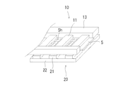
図2は、ピボット軸39の外側面における、フレキシャ10の端子部Tにおけるフライングリード11と、主フレキシブル配線板20の接続パッド部Kにおける端子(電極)21とが、異方性導電フィルム(ACF:Anisotropic Conductive Film)5を介在させることで導電接続された導電接続部または配線板の接続構造Jを示す図である。図2(a)が平面図で、図2(b)はIIB−IIB線に沿う断面図である。
主フレキシブル配線板20の接続パッド部Kでは、絶縁層またはカバーレイ23を除去され、基材22上の端子21は、開口側および側面で露出している。端子21は、絶縁層23の狭間の底において、基材22上に位置する。すなわち端子21は、絶縁層23で囲まれた凹部の底に位置する。
なお、ここで凹部とは、四方が絶縁層で囲まれていなくてもよく、たとえば対向する二方面に絶縁層が位置しており、いわゆる狭間であってもよい。
2 shows that the flying
In the connection pad portion K of the main
Here, the recess may not be surrounded by an insulating layer on all four sides, for example, the insulating layer may be located on two opposite sides, and may be a so-called gap.
図2(a)、(b)に示すように、本実施の形態における特徴は、次のとおりである。
(1)フライングリード11と端子21との導電接続は、ACF5を間に介在させることで実現されている。
(2)ACF5には、フライングリード11と端子21との間に挟まれて圧縮圧着された部分5aの周囲に、開口5hが配置された開口パターンが設けられている。
(3)フライングリード11および端子21を覆って補強するために配置した樹脂7は、ACF5の開口5hを通って、接続パッド部Kの基材22にまで届いて基材22に接着している。ACF5は、圧着された部分5a、開口5h、および非圧縮部5cを含んでいる。
上記の特徴の結果、樹脂7による強固な補強が形成されて、フライングリード11と端子21とが離間するおそれは無くなり、高い耐久性で導電接続が保持される。さらに、ACF5を用いることで簡単に信頼性の高い導電接続を得ることができる。
なお、上記の開口5hは、導電接続部の周りに配置されるものがあれば、他の開口5hが、熱圧着部にあってもよい。すなわち開口5hの加工精度はそれほど必要なく、少なくとも導電接続部の周りにあれば問題ない。
As shown in FIGS. 2A and 2B, the features in the present embodiment are as follows.
(1) The conductive connection between the flying
(2) The
(3) The
As a result of the above characteristics, strong reinforcement by the
In addition, as long as said
従来の接続構造では、フライングリード11がフラットであって、絶縁層13の延長部に含まれるように並行する部分からなるので、次の問題があった。超音波接合などで接合するとき、接合相手の接続パッド部K内の底に位置する端子21に接触させるためにフライングリード11に押し込み力を加えて押さえ込んで接合していた。しかしながら押さえ込まれたフライングリード11には、元のフラット形状に、部分的または大きく、戻るように復元力が生じて接続部が離間して接続不良を生じることがあった。
In the conventional connection structure, since the flying
しかし、図2(a)、(b)に示すように、本実施の形態では、補強のための樹脂7を用いた上で、その樹脂が接続パッド部Kの底を形成する基材22に届いてその基材22に接着するの。この結果、図2(b)に見られるように、樹脂7による強固な補強が形成される。
図2では、補強用の樹脂7は接続パッド部Kの全体に配置してあるが、接続パッド部Kの全体ではなく、所定の領域のフライングリード11/端子21に限定して補強用の樹脂7を配置してもよい。また、図2では、補強用の樹脂7は、接続パッド部Kの全体に連続しているが、導電接続された1対のフライングリード11/端子21ごとに分かれていてもよい。実施の形態2において、そのような例を示す。
However, as shown in FIGS. 2A and 2B, in the present embodiment, after the
In FIG. 2, the reinforcing
フレキシブル配線板10のフライングリード11は、絶縁層13から導体パターンを剥き出しにしたものである。フレキシブル配線板10の絶縁層13、主フレキシブル配線板20の基材22およびカバーレイ23には、たとえばポリイミド、ポリエステル等の、フレキシブル配線板用として汎用性のある樹脂を使用することができる。また、特に、柔軟性に加えて高い耐熱性をも有していることが好ましく、このような樹脂としては、例えば、ポリアミド系の樹脂や、ポリイミド、ポリアミドイミド等のポリイミド系の樹脂が好適に使用される。絶縁層13、基材22、カバーレイ23の厚みは、1〜30μmとするのがよい。
導体パターンまたはフライングリード11、もしくは端子21には、銅箔などの金属を用いることができる。超音波接続する場合には、金めっき層を形成するのがよい。金めっき層の下地に銅、ニッケルめっき層を形成することができる。端子21の厚みは、10μm〜30μmの範囲、たとえば18μmとするのがよい。また、フライングリード25の厚みは、10μm〜25μmの範囲、たとえば20μmとするのがよい。
The flying
A metal such as a copper foil can be used for the conductor pattern or the flying
図3は、フレキシャ10のフライングリード11と、主フレキシブル配線板20の端子21との接続部Jを形成する方法を示すフローチャートである。フライングリード11を備えるフレキシブル配線板10に、サスペンション板等を付け加えて複合体のフレキシャ(サスペンション)を形成する。このフレキシャ10のフライングリード11と、主フレキシブル配線板20の端子21とを導電接続する。
一方、ACF5については、予め、圧着される領域5aの周りに開口5hが設けられた開口パターンを形成しておく。ACF5は、導電性粒子を含有した異方導電性を有する異方導電性接着剤であって、熱硬化性接着樹脂を用いる場合は、エポキシ樹脂、高分子量エポキシ樹脂であるフェノキシ樹脂、硬化剤、及び導電性粒子を必須成分とする熱硬化性の接着剤である。ACF5としては、例えば、絶縁性の熱硬化性樹脂であるエポキシ樹脂およびフェノキシ樹脂を主成分とし、ニッケル、銅、銀、金等の導電性粒子が分散されたものが使用できる。エポキシ樹脂を使用することにより、ACF5のフィルム形成性、耐熱性、および接着力を向上させることが可能となる。ACF5の厚みは、30μm〜45μmの範囲、たとえば35μmとするのがよい。
FIG. 3 is a flowchart showing a method of forming the connection portion J between the flying
On the other hand, for the
ACF5に含有されるエポキシ樹脂としては、例えば、ビスフェノールA型、F型、S型、AD型、またはビスフェノールA型とビスフェノールF型との共重合型のエポキシ樹脂や、ナフタレン型エポキシ樹脂、ノボラック型エポキシ樹脂、ビフェニル型エポキシ樹脂、ジシクロペンタジエン型エポキシ樹脂等を使用することができる。また、ACF5は、上述のエポキシ樹脂のうち、少なくとも1種を含有していればよい。 Examples of the epoxy resin contained in ACF5 include bisphenol A type, F type, S type, AD type, or a copolymer type epoxy resin of bisphenol A type and bisphenol F type, naphthalene type epoxy resin, and novolak type. An epoxy resin, a biphenyl type epoxy resin, a dicyclopentadiene type epoxy resin, or the like can be used. Moreover, ACF5 should just contain at least 1 sort (s) among the above-mentioned epoxy resins.
また、エポキシ樹脂及びフェノキシ樹脂の分子量は、ACF5に要求される性能を考慮して、適宜選択することができる。例えば、高分子量のエポキシ樹脂を使用すると、フィルム形成性が高く、また、接続温度における樹脂の溶融粘度を高くでき、後述の導電性粒子の配向を乱すことなく接続できる効果がある。一方、低分子量のエポキシ樹脂を使用すると、架橋密度が高まって耐熱性が向上するという効果が得られる。また、加熱時に、上述の硬化剤と速やかに反応し、接着性能を高めるという効果が得られる。従って、分子量が15000以上の高分子量エポキシ樹脂と分子量が2000以下の低分子量エポキシ樹脂とを組み合わせて使用することが、性能のバランスが取れるため、好ましい。なお、高分子量エポキシ樹脂と低分子量エポキシ樹脂の配合量は、適宜、選択することができる。 The molecular weights of the epoxy resin and the phenoxy resin can be appropriately selected in consideration of the performance required for ACF5. For example, when a high molecular weight epoxy resin is used, the film forming property is high, the melt viscosity of the resin at the connection temperature can be increased, and there is an effect that the connection can be made without disturbing the orientation of the conductive particles described later. On the other hand, when a low molecular weight epoxy resin is used, the effect of increasing the crosslink density and improving the heat resistance is obtained. Moreover, the effect of reacting with the above-mentioned hardening | curing agent rapidly at the time of a heating, and improving adhesive performance is acquired. Therefore, it is preferable to use a combination of a high molecular weight epoxy resin having a molecular weight of 15000 or more and a low molecular weight epoxy resin having a molecular weight of 2000 or less because the balance of performance can be achieved. In addition, the compounding quantity of a high molecular weight epoxy resin and a low molecular weight epoxy resin can be selected suitably.
また、ACF5は、硬化剤として潜在性硬化剤を含有しており、エポキシ樹脂の硬化を促進させるための硬化剤を含有することにより、高い接着力を得ることができる。潜在性硬化剤は、低温での貯蔵安定性に優れ、室温では殆ど硬化反応を起こさないが、熱や光等により、速やかに硬化反応を行う硬化剤である。このような潜在性硬化剤としては、イミダゾール系、ヒドラジド系、三フッ化ホウ素−アミン錯体、アミンイミド、ポリアミン系、第3級アミン、アルキル尿素系等のアミン系、ジシアンジアミド系、酸無水物系、フェノール系、および、これらの変性物が例示され、これらは単独または2種以上の混合物として使用できる。 Moreover, ACF5 contains a latent curing agent as a curing agent, and a high adhesive force can be obtained by containing a curing agent for promoting the curing of the epoxy resin. A latent curing agent is a curing agent that is excellent in storage stability at low temperatures and hardly undergoes a curing reaction at room temperature, but rapidly undergoes a curing reaction by heat, light, or the like. Examples of such latent curing agents include imidazole, hydrazide, boron trifluoride-amine complexes, amine imides, polyamines, tertiary amines, alkyl ureas, and other amines, dicyandiamides, acid anhydrides, Phenol-based compounds and modified products thereof are exemplified, and these can be used alone or as a mixture of two or more.
ACF5には導電性粒子が分散されており、導電性粒子は、微細な金属粒子(例えば、球状の金属微粒子や金属でメッキされた球状の樹脂粒子からなる金属微粒子)が多数、直鎖状に繋がった形状、または針形状を有する、所謂アスペクト比が大きい形状を有する金属粉末により形成されている。また、本実施の形態においては、ACF33に占める導電性粒子の割合は、0.0001体積%以上0.2体積%以下とするのがよい。
上記は、ACF5に熱硬化性接着剤を用いた場合について詳しく説明したが、熱可塑性樹脂を用いてもよいことは、上記のとおりである。
Conductive particles are dispersed in ACF5, and the conductive particles include a large number of fine metal particles (for example, metal particles made of spherical metal particles or spherical resin particles plated with metal) in a linear form. It is formed of a metal powder having a connected shape or a needle shape, a shape having a large so-called aspect ratio. In the present embodiment, the proportion of conductive particles in ACF 33 is preferably 0.0001% by volume or more and 0.2% by volume or less.
Although the above explained in detail about the case where a thermosetting adhesive was used for ACF5, it is as above-mentioned that a thermoplastic resin may be used.
接続パッド部Kにおいて、端子21/ACF5の圧着される領域5a/フライングリード11、の位置が合うように調整したあと、熱圧着ツール(図示せず)をフライングリード11の上から押し当てて、加熱しながら圧着する。図4は、熱圧着されて導電接続された状態を示す図である。
この状態のままでは、上述のようにフライングリード11の復元力によって、時間の経過につれて当該フライングリード11と端子21との離間が生じるおそれがある。この離間を防止するために、上記のように補強用の樹脂7を配置する。
In the connection pad portion K, after adjusting so that the position of the terminal 21 / ACF5 to be crimped 5a / flying
In this state, the flying
樹脂7については次の点が重要である。まず樹脂7としては、どのような樹脂でもよいが、たとえば絶縁性の熱硬化性樹脂であるエポキシ樹脂、フェノキシ樹脂などを用いるのがよい。これらの樹脂を溶剤(溶媒)中に希釈して、粘度を調整する。溶剤は、これらの樹脂をその溶剤中に溶解させたあと、塗布接着後に乾燥固化できるものならば何でもよい。たとえば溶剤には、ケトン系としてはシクロヘキサン、イソホロンなど、エステル系としては酢酸ブチルなど、またエーテル+エステル系としてはセロソルブアセテート、プロプレングリコールモノメチルエーテルアセテート、ブチルカルビトールアセテート、カルビトールアセテートなど、を挙げることができる。上記以外の溶剤に、芳香族系、アミド系、などを用いてもよい。
粘度の調整は、接続パッド部K全体に連続して樹脂を配置する場合は粘度は小さく、また、特定の領域に限定して補強用の樹脂を配置する場合は基材22に濡れて広がらないように粘度は高めに調整するのがよい。
図4の状態の接続パッド部K(実際は、カバーレイ23で囲まれている)に位置するフライングリード11を覆うように樹脂を流す。接続パッド部Kを適当に傾けて樹脂の流れを適正にする。その後、加熱処理して溶媒を放散して硬化させる。これによって、基材22に接着された導電接続部(端子21/ACF5a/フライングリード11)を被覆する補強用の樹脂7が形成される。
The following points are important for the
In the adjustment of the viscosity, when the resin is continuously arranged over the entire connection pad portion K, the viscosity is small, and when the resin for reinforcement is arranged only in a specific region, the
Resin is allowed to flow so as to cover the flying leads 11 located in the connection pad portion K (actually surrounded by the coverlay 23) in the state of FIG. The connection pad portion K is appropriately tilted to make the resin flow appropriate. Then, it heat-processes and a solvent is dissipated and hardened. As a result, the reinforcing
(実施の形態2)
図5は、本発明の実施の形態2の配線板の接続構造Jを示す図である。図5(a)は平面図、また図5(b)はVB−VB線に沿う断面図である。実施の形態1(図2参照)では、補強用の樹脂7は、接続パッド部Kの全体に連続する形態をとった。本実施の形態では、接続パッド部Kの所定の領域に限定して、その領域の導電接続されたフライングリード11/端子21を被覆する、補強用の樹脂7を配置する点に特徴がある。
図5(a)に示すように、樹脂7は、限定された領域の(フライングリード11/ACF5a/端子21)を被覆して、その領域内でACF5の開口5hを通って主フレキシブル配線板20の基材22にまで届き、その基材22に接着している。
これによって、たとえばフライングリード11/ACF5a/端子21において、最も離間が生じやすい領域を狙いうちにして、強力な補強用の樹脂7を配置することができる。
(Embodiment 2)
FIG. 5 is a diagram showing a wiring board connection structure J according to the second embodiment of the present invention. 5A is a plan view, and FIG. 5B is a cross-sectional view taken along the line VB-VB. In the first embodiment (see FIG. 2), the reinforcing
As shown in FIG. 5 (a), the
As a result, for example, in the flying
(実施の形態3)
図6は、本発明の実施の形態3の配線板の接続構造Jを示す図である。本実施の形態では、次の点に特徴を有する。
(1)ACF5の面積を接続パッド部Kの面積より大きく縮小して、フライングリード11の中央部を含む領域に限定した。フライングリード11の端(すなわち絶縁層13に覆われる部分に続く部分)では、元来、端子21から基材(図示せず)の厚み分だけ離れているので、導電接続に寄与しにくい。ACF5は高価であり、経済性を高めるために、使用する面積は小さいほうが望ましい。これらのことを考慮すると、図6に示すように、フライングリードの端に対応する領域にACF5を配置しないで、中央部を含む領域に限定してACF5を配置することは合理性にかなっている。
(2)補強用の樹脂7は、フライングリード11の復元力に対して効果的に対抗できる位置、たとえばフライングリード11の中央部分に限定して配置した。フライングリード11の中央部分に、強力な補強用の樹脂7を配置する。この補強用の樹脂7は、ACF5の開口5hを通って基材22にまで届き当該基材22に接着した上で、端子21/ACF5a/フライングリード11、を被覆している。
本実施の形態により、経済性を高めた上で、耐久性に優れた配線板の接続構造Jを得ることができる。上記の導電接続は、ACF5を介在させて行うため、非常に簡単に遂行することができる。
(Embodiment 3)
FIG. 6 is a diagram showing a wiring board connection structure J according to the third embodiment of the present invention. This embodiment is characterized by the following points.
(1) The area of the
(2) The reinforcing
According to the present embodiment, it is possible to obtain a wiring board connection structure J excellent in durability while improving economy. Since the above-described conductive connection is performed with the
(実施の形態4)
図7は、本発明の実施の形態4の配線板の接続構造Jを示す図である。本実施の形態では、次の点に特徴を有する。
(1)ACF5の巾をフライングリード11の長手方向の長さよりも狭くして、1本だけ、配置している。ACF5の巾が狭いため、接続パッド部K内において、そのACF5とカバーレイ13,23との間に側部スペースSpを生じている。
(2)補強用の樹脂7は、導電接続部のフライングリード11の上から被覆するように配置され、側部スペースSpから接続パッド部Kの底部の基材22に到達してその基材22に接着する。
(3)ACF5は、フライングリード11の中央付近でのみ、そのフライングリード11と端子21との間に介在する。このフライングリード11の中央付近は、フライングリード11が最も端子21の側に張り出しやすい箇所である。すなわち中央付近で、フライングリード11と端子21との導電接続を確保しやすい。この部分において確実な導電接続を実現した上で、樹脂7による補強をすることで耐久性にある導電接続を簡単に実現することができる。
(Embodiment 4)
FIG. 7 is a diagram showing a wiring board connection structure J according to the fourth embodiment of the present invention. This embodiment is characterized by the following points.
(1) The width of the
(2) The reinforcing
(3) The
図8および図9は、実施の形態1における図3および図4に対応する製造段階の図である。本実施の形態では、ACF5の巾は、フライングリード11の長さよりも相当小さくする。たとえばフライングリード11の長さまたは接続パッド部Kの短辺の、1/2以下にする。ACF5には、その他の加工はされない。巾を狭くした結果、図9に示すように、熱圧着されたあと、導電接続部のACF5の側部にスペースSpができる。この側部スペースSpを通って、フライングリード11の上から被覆するように配置された樹脂7は、非常に容易に基材22に到達してその基材22に接着することができる。
被覆するとき溶媒に希釈された樹脂7の粘度は、実施の形態1等の開口パターンから基材22に到達させる場合よりも、より高く(硬めに)するのがよい。
8 and 9 are diagrams of manufacturing stages corresponding to FIGS. 3 and 4 in the first embodiment. In the present embodiment, the width of the
The viscosity of the
高価なACF5の面積(量)は少なくて済み、また、そのACF5に開口5hを設ける工程などは必要はない。巾を狭くする工程のみが必要であるが、簡単な作業で済ますことができる。この結果、経済性に優れた導電接続構造Jを得ることができる。
The area (amount) of the
(その他の実施の形態)
実施の形態1〜4は、HDD用のフレキシブル配線板および接続構造について説明した。しかし、本発明の配線板の接続構造は、HDD用に限定されず、その他の汎用および特殊用途のものに用いることができる。
(Other embodiments)
In the first to fourth embodiments, the flexible wiring board for HDD and the connection structure have been described. However, the connection structure of the wiring board of the present invention is not limited to the HDD, and can be used for other general purpose and special purposes.
上記において、本発明の実施の形態および実施例について説明を行ったが、上記に開示された本発明の実施の形態および実施例は、あくまで例示であって、本発明の範囲はこれら発明の実施の形態に限定されない。本発明の範囲は、特許請求の範囲の記載によって示され、さらに特許請求の範囲の記載と均等の意味および範囲内でのすべての変更を含むものである。 Although the embodiments and examples of the present invention have been described above, the embodiments and examples of the present invention disclosed above are merely examples, and the scope of the present invention is the implementation of these inventions. It is not limited to the form. The scope of the present invention is indicated by the description of the scope of claims, and further includes meanings equivalent to the description of the scope of claims and all modifications within the scope.
本発明の配線板の接続構造等によれば、凹部または狭間をなす接続パッド部の底部に位置する端子と、フレキシブル配線板のフライングリードとを、ACFを用いて、簡単かつ確実に接続して耐久性のある接続部を得ることができる。ACFを用いることで導電接続の作業を簡単かつ容易に遂行できる。さらに、経済性と信頼性を両立できるように、ACFの使用面積を縮小して効果的な箇所に限定して使用し、補強用の樹脂を用いて導電接続の耐久性を確保することができる。 According to the wiring board connection structure or the like of the present invention, the terminal located at the bottom of the connection pad part that forms the recess or the gap and the flying lead of the flexible wiring board are simply and reliably connected using the ACF. A durable connection can be obtained. By using the ACF, the conductive connection work can be easily and easily performed. Furthermore, in order to achieve both economy and reliability, it is possible to reduce the use area of the ACF and use it limited to an effective location, and to ensure the durability of the conductive connection by using a reinforcing resin. .
5 ACF、5a ACFの圧着部、5c ACFの非圧着部、5h ACFの開口、7 樹脂、10 フレキシブル配線板(フレキシャ)、11 フライングリード(露出リード)、13 絶縁層(カバーレイ)、15 サスペンション板、18 導体(配線)パターン、19 ヘッドスライダ、20 主フレキシブル配線板、21 端子、22 主フレキシブル配線板の基材、23 主フレキシブル配線板のカバーレイ、29 主フレキシブル配線板の端、31 ヘッド支持体、32 アーム、33 ボイスコイル、39 ピボット(揺動)軸、50 APFA、90 磁気ディスク、100 HDD、K 主フレキシブル配線板の接続パッド部、T フレキシャの端子部、J 接続部、Sp 側部スペース。 5 ACF, 5a ACF crimping part, 5c ACF non-crimping part, 5h ACF opening, 7 resin, 10 flexible wiring board (flexure), 11 flying lead (exposed lead), 13 insulating layer (coverlay), 15 suspension Board, 18 Conductor (wiring) pattern, 19 Head slider, 20 Main flexible wiring board, 21 Terminal, 22 Main flexible wiring board base material, 23 Main flexible wiring board coverlay, 29 Main flexible wiring board end, 31 Head Support, 32 arms, 33 voice coil, 39 pivot (swing) shaft, 50 APFA, 90 magnetic disk, 100 HDD, K connection pad of main flexible wiring board, T flexure terminal, J connection, Sp side Department space.
Claims (7)
絶縁層が抜かれた端子部において導体パターンが露出された露出リードを有するフレキシブル配線板と、
前記露出リードと前記基材上の端子との間に介在して導電接続する異方性導電フィルム(ACF:Anisotropic Conductive Film)と、
前記導電接続された部分の前記露出リードおよび端子を覆うように位置する樹脂とを備え、
前記異方性導電フィルムの前記導電接続部の周りに開口があり、該開口を通って、前記導電接続部の前記露出リードおよび端子を覆う樹脂は連続して前記接続パッド部の底部をなす基材に接着していることを特徴とする、配線板の接続構造。 A wiring board having a connection pad portion in which terminals are arranged on the base material at the bottom from which the insulating layer is removed;
A flexible wiring board having an exposed lead in which the conductor pattern is exposed at the terminal portion from which the insulating layer has been removed;
An anisotropic conductive film (ACF) that is electrically conductively connected between the exposed lead and the terminal on the substrate;
A resin positioned so as to cover the exposed lead and the terminal of the conductively connected portion;
There is an opening around the conductive connection portion of the anisotropic conductive film, and the resin covering the exposed lead and the terminal of the conductive connection portion continuously forms the bottom of the connection pad portion through the opening. Wiring board connection structure, characterized by being bonded to a material.
前記接続パッド部の寸法に合った寸法、またはそれより小さい寸法、をもつ異方性導電フィルムに対して、前記接続パッド部の端子に対応する領域の周囲に開口を設ける工程と、
前記配線板の接続パッド部の上に、前記異方性導電フィルムを、前記端子に対応する領域をその端子に重ねるように位置合わせして配置し、その異方性導電フィルムの上に、前記フレキシブル配線板を、前記露出リードが前記端子に重なるように位置合わせして配置して、熱圧着ツールによって加熱加圧して圧着する工程と、
前記熱圧着によって導電接続された部分の露出リードを覆うように、溶媒に希釈された樹脂を配置しつつ、該希釈された樹脂を前記異方性導電フィルムの前記開口を通して前記接続パッドの底部に届かせ、その後、溶媒を放散させて固化する加熱処理を行うことを特徴とする、配線板の接続構造。 Preparing a flexible wiring board having exposed leads and a wiring board having terminals on the base material of the bottom of the connection pad part; and
Providing an opening around a region corresponding to a terminal of the connection pad portion for an anisotropic conductive film having a size matching the size of the connection pad portion or a size smaller than the size,
On the connection pad portion of the wiring board, the anisotropic conductive film is disposed so as to be aligned so that a region corresponding to the terminal is superimposed on the terminal, and on the anisotropic conductive film, the Arranging the flexible wiring board so that the exposed lead overlaps the terminal, and heat-pressing with a thermocompression-bonding tool, and crimping;
A resin diluted with a solvent is disposed so as to cover the exposed lead of the portion electrically connected by the thermocompression bonding, and the diluted resin is placed on the bottom of the connection pad through the opening of the anisotropic conductive film. A connection structure for a wiring board, which is subjected to a heat treatment that causes the solvent to disperse and then solidifies by dissipating the solvent.
Priority Applications (1)
| Application Number | Priority Date | Filing Date | Title |
|---|---|---|---|
| JP2011010889A JP5787249B2 (en) | 2011-01-21 | 2011-01-21 | Wiring board connection structure, formation method thereof, and HDD |
Applications Claiming Priority (1)
| Application Number | Priority Date | Filing Date | Title |
|---|---|---|---|
| JP2011010889A JP5787249B2 (en) | 2011-01-21 | 2011-01-21 | Wiring board connection structure, formation method thereof, and HDD |
Publications (2)
| Publication Number | Publication Date |
|---|---|
| JP2012150872A true JP2012150872A (en) | 2012-08-09 |
| JP5787249B2 JP5787249B2 (en) | 2015-09-30 |
Family
ID=46792984
Family Applications (1)
| Application Number | Title | Priority Date | Filing Date |
|---|---|---|---|
| JP2011010889A Active JP5787249B2 (en) | 2011-01-21 | 2011-01-21 | Wiring board connection structure, formation method thereof, and HDD |
Country Status (1)
| Country | Link |
|---|---|
| JP (1) | JP5787249B2 (en) |
Cited By (3)
| Publication number | Priority date | Publication date | Assignee | Title |
|---|---|---|---|---|
| JP2014208793A (en) * | 2013-03-29 | 2014-11-06 | 住友電気工業株式会社 | Polyimide precursor resin composition, polyimide resin film, flexible printed wiring board, circuit-fitted suspension, and hard disc drive |
| US9496625B2 (en) | 2014-05-21 | 2016-11-15 | Nhk Spring Co., Ltd. | Terminal connection structure with elevated terminals |
| WO2020202358A1 (en) * | 2019-03-29 | 2020-10-08 | オリンパス株式会社 | Ultrasonic transducer, ultrasonic endoscope, and method for manufacturing ultrasonic transducer |
Citations (3)
| Publication number | Priority date | Publication date | Assignee | Title |
|---|---|---|---|---|
| JPH0212988A (en) * | 1988-06-30 | 1990-01-17 | Nec Corp | Connecting method for flexible printed circuit |
| JPH104248A (en) * | 1996-06-17 | 1998-01-06 | Teikoku Tsushin Kogyo Co Ltd | Board connection structure |
| JP2000207719A (en) * | 1999-01-12 | 2000-07-28 | Nitto Denko Corp | Connection structure between suspension board with circuit and printed circuit board |
-
2011
- 2011-01-21 JP JP2011010889A patent/JP5787249B2/en active Active
Patent Citations (3)
| Publication number | Priority date | Publication date | Assignee | Title |
|---|---|---|---|---|
| JPH0212988A (en) * | 1988-06-30 | 1990-01-17 | Nec Corp | Connecting method for flexible printed circuit |
| JPH104248A (en) * | 1996-06-17 | 1998-01-06 | Teikoku Tsushin Kogyo Co Ltd | Board connection structure |
| JP2000207719A (en) * | 1999-01-12 | 2000-07-28 | Nitto Denko Corp | Connection structure between suspension board with circuit and printed circuit board |
Cited By (6)
| Publication number | Priority date | Publication date | Assignee | Title |
|---|---|---|---|---|
| JP2014208793A (en) * | 2013-03-29 | 2014-11-06 | 住友電気工業株式会社 | Polyimide precursor resin composition, polyimide resin film, flexible printed wiring board, circuit-fitted suspension, and hard disc drive |
| US9496625B2 (en) | 2014-05-21 | 2016-11-15 | Nhk Spring Co., Ltd. | Terminal connection structure with elevated terminals |
| WO2020202358A1 (en) * | 2019-03-29 | 2020-10-08 | オリンパス株式会社 | Ultrasonic transducer, ultrasonic endoscope, and method for manufacturing ultrasonic transducer |
| JPWO2020202358A1 (en) * | 2019-03-29 | 2021-12-16 | オリンパス株式会社 | Manufacturing method of ultrasonic vibrator, ultrasonic endoscope and ultrasonic vibrator |
| JP7109654B2 (en) | 2019-03-29 | 2022-07-29 | オリンパス株式会社 | Ultrasonic transducer, ultrasonic endoscope, and method for manufacturing ultrasonic transducer |
| US11872081B2 (en) | 2019-03-29 | 2024-01-16 | Olympus Corporation | Ultrasound transducer, ultrasound endoscope, and manufacturing method of ultrasound transducer |
Also Published As
| Publication number | Publication date |
|---|---|
| JP5787249B2 (en) | 2015-09-30 |
Similar Documents
| Publication | Publication Date | Title |
|---|---|---|
| US5896248A (en) | Bond pads for metal welding of flexure to air bearing slider and grounding configuration thereof | |
| US8760812B1 (en) | Disk drive head gimbal assembly having a jumper in a flexible printed circuit overlap region | |
| CN102915746B (en) | Cantilever part, magnetic head folding piece combination and hard disk drive unit | |
| US8295014B1 (en) | Disk drive head gimbal assembly having a flexure tail with transverse flying leads | |
| CN104240725B (en) | Disk drive suspension | |
| JP2006049751A (en) | Magnetic disk drive, wiring connection structure and terminal structure thereof | |
| CN102208191A (en) | Electronic apparatus and disk drive suspension | |
| JP5787249B2 (en) | Wiring board connection structure, formation method thereof, and HDD | |
| JP2001500668A (en) | Circuit connector | |
| WO2012102091A1 (en) | Printed-circuit-board connection structure, head stack assembly provided with printed-circuit-board connection structure, magnetic disk provided with head stack assembly, and method of manufacturing printed-circuit-board connection structure | |
| JP5831803B2 (en) | Suspension board, suspension, suspension with head and hard disk drive | |
| CN108962287A (en) | The circuit block of disk drive suspension | |
| JP2012146353A (en) | Flexible wiring board, connection structure of wiring board and method of manufacturing thereof | |
| US7420784B2 (en) | Rotating disk storage device with high rigidity flexible printed circuit board | |
| US7682879B2 (en) | Edge coating a microelectronic device | |
| JP4123321B2 (en) | Wiring board bonding method | |
| CN212954989U (en) | Conductive adhesive | |
| JP2012160535A (en) | Printed wiring board connection structure, head stack assembly with printed wiring board connection structure, magnetic disk device with head stack assembly, and method for manufacturing printed wiring board connection structure | |
| JP2017162543A (en) | Substrate for suspension, suspension, suspension with head and hard disk drive | |
| JP7763671B2 (en) | Terminal connections of electronic devices | |
| JP6187883B2 (en) | Suspension board, suspension, suspension with head and hard disk drive | |
| JP5704485B2 (en) | Printed wiring board connection structure, head stack assembly including the printed wiring board connection structure, magnetic disk device including the head stack assembly, and method for manufacturing the printed wiring board connection structure | |
| JP2012155803A (en) | Connection structure of printed wiring board, head stack assembly with connection structure of printed wiring board, magnetic disk drive with head stack assembly, and method of manufacturing connection structure of printed wiring board | |
| JP6128439B2 (en) | Multi-sided suspension board, suspension board, suspension, suspension with head and hard disk drive | |
| JP2544580B2 (en) | Magnetic head assembly, manufacturing method thereof, and magnetic disk device |
Legal Events
| Date | Code | Title | Description |
|---|---|---|---|
| A625 | Written request for application examination (by other person) |
Free format text: JAPANESE INTERMEDIATE CODE: A625 Effective date: 20140106 |
|
| A977 | Report on retrieval |
Free format text: JAPANESE INTERMEDIATE CODE: A971007 Effective date: 20141226 |
|
| A131 | Notification of reasons for refusal |
Free format text: JAPANESE INTERMEDIATE CODE: A131 Effective date: 20150127 |
|
| A521 | Request for written amendment filed |
Free format text: JAPANESE INTERMEDIATE CODE: A523 Effective date: 20150303 |
|
| TRDD | Decision of grant or rejection written | ||
| A01 | Written decision to grant a patent or to grant a registration (utility model) |
Free format text: JAPANESE INTERMEDIATE CODE: A01 Effective date: 20150706 |
|
| A61 | First payment of annual fees (during grant procedure) |
Free format text: JAPANESE INTERMEDIATE CODE: A61 Effective date: 20150717 |
|
| R150 | Certificate of patent or registration of utility model |
Ref document number: 5787249 Country of ref document: JP Free format text: JAPANESE INTERMEDIATE CODE: R150 |
|
| R250 | Receipt of annual fees |
Free format text: JAPANESE INTERMEDIATE CODE: R250 |
|
| R250 | Receipt of annual fees |
Free format text: JAPANESE INTERMEDIATE CODE: R250 |
|
| R250 | Receipt of annual fees |
Free format text: JAPANESE INTERMEDIATE CODE: R250 |
|
| R250 | Receipt of annual fees |
Free format text: JAPANESE INTERMEDIATE CODE: R250 |
|
| R250 | Receipt of annual fees |
Free format text: JAPANESE INTERMEDIATE CODE: R250 |
|
| R250 | Receipt of annual fees |
Free format text: JAPANESE INTERMEDIATE CODE: R250 |
|
| R250 | Receipt of annual fees |
Free format text: JAPANESE INTERMEDIATE CODE: R250 |
|
| R250 | Receipt of annual fees |
Free format text: JAPANESE INTERMEDIATE CODE: R250 |