JP2011519173A - (W) Light converter system for LED - Google Patents
(W) Light converter system for LED Download PDFInfo
- Publication number
- JP2011519173A JP2011519173A JP2011506606A JP2011506606A JP2011519173A JP 2011519173 A JP2011519173 A JP 2011519173A JP 2011506606 A JP2011506606 A JP 2011506606A JP 2011506606 A JP2011506606 A JP 2011506606A JP 2011519173 A JP2011519173 A JP 2011519173A
- Authority
- JP
- Japan
- Prior art keywords
- converter
- optical component
- further characterized
- optical
- glass
- Prior art date
- Legal status (The legal status is an assumption and is not a legal conclusion. Google has not performed a legal analysis and makes no representation as to the accuracy of the status listed.)
- Granted
Links
Images


Classifications
-
- H—ELECTRICITY
- H10—SEMICONDUCTOR DEVICES; ELECTRIC SOLID-STATE DEVICES NOT OTHERWISE PROVIDED FOR
- H10H—INORGANIC LIGHT-EMITTING SEMICONDUCTOR DEVICES HAVING POTENTIAL BARRIERS
- H10H20/00—Individual inorganic light-emitting semiconductor devices having potential barriers, e.g. light-emitting diodes [LED]
- H10H20/80—Constructional details
- H10H20/85—Packages
- H10H20/851—Wavelength conversion means
- H10H20/8511—Wavelength conversion means characterised by their material, e.g. binder
- H10H20/8512—Wavelength conversion materials
-
- C—CHEMISTRY; METALLURGY
- C03—GLASS; MINERAL OR SLAG WOOL
- C03B—MANUFACTURE, SHAPING, OR SUPPLEMENTARY PROCESSES
- C03B11/00—Pressing molten glass or performed glass reheated to equivalent low viscosity without blowing
- C03B11/06—Construction of plunger or mould
- C03B11/08—Construction of plunger or mould for making solid articles, e.g. lenses
- C03B11/082—Construction of plunger or mould for making solid articles, e.g. lenses having profiled, patterned or microstructured surfaces
-
- C—CHEMISTRY; METALLURGY
- C03—GLASS; MINERAL OR SLAG WOOL
- C03B—MANUFACTURE, SHAPING, OR SUPPLEMENTARY PROCESSES
- C03B19/00—Other methods of shaping glass
- C03B19/10—Forming beads
- C03B19/1005—Forming solid beads
- C03B19/101—Forming solid beads by casting molten glass into a mould or onto a wire
-
- C—CHEMISTRY; METALLURGY
- C03—GLASS; MINERAL OR SLAG WOOL
- C03B—MANUFACTURE, SHAPING, OR SUPPLEMENTARY PROCESSES
- C03B23/00—Re-forming shaped glass
-
- C—CHEMISTRY; METALLURGY
- C03—GLASS; MINERAL OR SLAG WOOL
- C03B—MANUFACTURE, SHAPING, OR SUPPLEMENTARY PROCESSES
- C03B23/00—Re-forming shaped glass
- C03B23/0013—Re-forming shaped glass by pressing
-
- H—ELECTRICITY
- H10—SEMICONDUCTOR DEVICES; ELECTRIC SOLID-STATE DEVICES NOT OTHERWISE PROVIDED FOR
- H10F—INORGANIC SEMICONDUCTOR DEVICES SENSITIVE TO INFRARED RADIATION, LIGHT, ELECTROMAGNETIC RADIATION OF SHORTER WAVELENGTH OR CORPUSCULAR RADIATION
- H10F55/00—Radiation-sensitive semiconductor devices covered by groups H10F10/00, H10F19/00 or H10F30/00 being structurally associated with electric light sources and electrically or optically coupled thereto
- H10F55/10—Radiation-sensitive semiconductor devices covered by groups H10F10/00, H10F19/00 or H10F30/00 being structurally associated with electric light sources and electrically or optically coupled thereto wherein the radiation-sensitive semiconductor devices control the electric light source, e.g. image converters, image amplifiers or image storage devices
- H10F55/15—Radiation-sensitive semiconductor devices covered by groups H10F10/00, H10F19/00 or H10F30/00 being structurally associated with electric light sources and electrically or optically coupled thereto wherein the radiation-sensitive semiconductor devices control the electric light source, e.g. image converters, image amplifiers or image storage devices wherein the radiation-sensitive devices and the electric light source are all semiconductor devices
- H10F55/155—Radiation-sensitive semiconductor devices covered by groups H10F10/00, H10F19/00 or H10F30/00 being structurally associated with electric light sources and electrically or optically coupled thereto wherein the radiation-sensitive semiconductor devices control the electric light source, e.g. image converters, image amplifiers or image storage devices wherein the radiation-sensitive devices and the electric light source are all semiconductor devices formed in, or on, a common substrate
-
- H—ELECTRICITY
- H10—SEMICONDUCTOR DEVICES; ELECTRIC SOLID-STATE DEVICES NOT OTHERWISE PROVIDED FOR
- H10H—INORGANIC LIGHT-EMITTING SEMICONDUCTOR DEVICES HAVING POTENTIAL BARRIERS
- H10H20/00—Individual inorganic light-emitting semiconductor devices having potential barriers, e.g. light-emitting diodes [LED]
- H10H20/80—Constructional details
- H10H20/85—Packages
- H10H20/855—Optical field-shaping means, e.g. lenses
-
- C—CHEMISTRY; METALLURGY
- C03—GLASS; MINERAL OR SLAG WOOL
- C03B—MANUFACTURE, SHAPING, OR SUPPLEMENTARY PROCESSES
- C03B2215/00—Press-moulding glass
- C03B2215/80—Simultaneous pressing of multiple products; Multiple parallel moulds
-
- H—ELECTRICITY
- H10—SEMICONDUCTOR DEVICES; ELECTRIC SOLID-STATE DEVICES NOT OTHERWISE PROVIDED FOR
- H10H—INORGANIC LIGHT-EMITTING SEMICONDUCTOR DEVICES HAVING POTENTIAL BARRIERS
- H10H20/00—Individual inorganic light-emitting semiconductor devices having potential barriers, e.g. light-emitting diodes [LED]
- H10H20/80—Constructional details
- H10H20/85—Packages
- H10H20/851—Wavelength conversion means
- H10H20/8515—Wavelength conversion means not being in contact with the bodies
-
- H10W90/756—
Landscapes
- Chemical & Material Sciences (AREA)
- Engineering & Computer Science (AREA)
- Materials Engineering (AREA)
- Organic Chemistry (AREA)
- Manufacturing & Machinery (AREA)
- Led Device Packages (AREA)
- Optical Couplings Of Light Guides (AREA)
Abstract
本発明は、好ましくはいわゆる(W)LED用であるLED用光コンバータ・システム、および前記光コンバータ・システムを製造する方法に関する。モジュール式光コンバータ・システムは、LEDによって放出された放射を変換するための無機コンバータと、LEDの放出方向でコンバータの下流に実装された好ましくはガラスを含む無機光学部品とを備え、コンバータと第1の光学部品とが、互いに接し、少なくとも部分的に接続される。光コンバータ・システムは、従来技術から知られているシステムを上回る耐温度性を有する。システムの好ましい構成要素は、実質的に耐UV性であり、化学的耐性を有する。 The present invention relates to a light converter system for LEDs, preferably for so-called (W) LEDs, and a method for manufacturing said light converter system. The modular light converter system comprises an inorganic converter for converting the radiation emitted by the LED, and an inorganic optical component, preferably comprising glass, mounted downstream of the converter in the LED emission direction. One optical component is in contact with each other and is at least partially connected. The optical converter system has a higher temperature resistance than the systems known from the prior art. Preferred components of the system are substantially UV resistant and chemically resistant.
Description
本発明は、LED、好ましくは、いわゆる(W)LED用光コンバータ・システムと、当該光コンバータ・システムを製造する方法に関する。 The present invention relates to a light converter system for an LED, preferably a so-called (W) LED, and a method of manufacturing the light converter system.
現在、LED、コンバータおよび光学素子を有するシステムは、いわゆる成型加工により、パッケージとも呼ばれる容器の中に一緒に配置される。よく知られている方法では、パッケージは、個々の構成要素から直接構成され、次いで、それらが互いにしっかりと接合される。一般に、シリコーン樹脂がこの目的に用いられる。そのようなシステムは、例えばドイツ特許第10 2005 009 066 A1号の文献の中に説明されている。
Currently, systems with LEDs, converters and optical elements are placed together in a container, also called a package, by a so-called molding process. In a well known method, the package is constructed directly from the individual components, which are then firmly joined together. In general, silicone resins are used for this purpose. Such a system is described, for example, in the
そのようなシステムの基本的には有機的特性に基づく不都合は、その耐温度性が劣ることであり、一般に約100℃の値しか達成されない。耐温度性が劣るため、そのようなシステムは特定の条件下でしかはんだ処理と適合せず、というのは、そのようなプロセスは、高熱の発生をもたらす、あるいは必要とするからである。具体的には、LEDチップで現在用いられているいわゆる接合温度が、現行の最高温度100〜150℃から200℃へ上昇すると、従来技術で用いられる材料をこれ以上利用することができない。 The disadvantage of such a system, which is basically based on organic properties, is its poor temperature resistance, generally only values of about 100 ° C. are achieved. Due to poor temperature resistance, such systems are compatible with solder processing only under certain conditions, because such processes result in or require the generation of high heat. Specifically, when the so-called junction temperature currently used in LED chips rises from the current maximum temperature of 100 to 150 ° C. to 200 ° C., the material used in the prior art cannot be used any more.
また、そのようなシステムはUVに対して耐性がない。さらに、そのようなパッケージは密閉されていることもなく、したがって湿気などの環境の影響を受けやすい。しかし、半導体部品の複雑さおよび様々な用途が増加することにより、気密形パッケージが必要とされる。この例には、LDおよび光検出器あるいはカラーモニタを有するLEDがある。 Also, such systems are not resistant to UV. Furthermore, such packages are not hermetically sealed and are therefore susceptible to environmental effects such as moisture. However, due to the increasing complexity of semiconductor components and various applications, hermetic packages are required. Examples of this include LEDs with LDs and photodetectors or color monitors.
既知のシステムの別の不都合は、それらが老化に強くないという事実に基づく。具体的には、プラスチックのいわゆる脱ガス効果が半導体チップの老化をもたらす。現在使用されている材料の場合、放射光の好ましくは低い波長が、光学的性質および付着メカニズムの劣化をもたらす。また、用いられるプラスチックの、特に1W/mK未満の範囲にある低い熱導電率も不都合である。 Another disadvantage of known systems is based on the fact that they are not resistant to aging. Specifically, the so-called degassing effect of plastic causes aging of the semiconductor chip. For currently used materials, the preferably low wavelength of the emitted light results in degradation of the optical properties and attachment mechanism. Also, the low thermal conductivity of the plastics used, especially in the range below 1 W / mK, is disadvantageous.
個々の構成要素は、一般に、互いにしっかりと接合されてパッケージで提供される。また、特に個々の構成要素の屈折率を、互いに柔軟に一致させること、および光の波長に対して柔軟に一致させることも、単に非常に困難であり、あるいは一般に不可能である。別の不都合に、個々の構成要素を組み立てなければならないので、製造における経費の増加がある。 The individual components are generally provided in a package that is firmly joined together. In particular, it is simply very difficult or generally impossible to flexibly match the refractive indices of the individual components to each other and to flexibly match the wavelength of light. Another disadvantage is the increase in manufacturing costs because the individual components must be assembled.
したがって、この背景に対して、本発明の目的は、具体的にはLED用または(W)LED用である放射を放出する構成要素向けの、少なくとも従来技術の前述の不都合を回避する光コンバータ・システムまたはコンバータ・モジュールおよびそのようなシステムの製造方法を提供することである。 Therefore, against this background, the object of the present invention is to provide an optical converter that avoids at least the aforementioned disadvantages of the prior art, in particular for components emitting radiation that are for LEDs or for (W) LEDs. It is to provide a system or converter module and a method of manufacturing such a system.
具体的には、本発明は、将来の技術的傾向にも適合するはずであり、大量生産にも特に適することになる。 Specifically, the present invention should be compatible with future technical trends and will be particularly suitable for mass production.
これらの目的は、このコンバータ・モジュールおよび独立請求項による方法によって達成される。有利な実施形態は、それぞれの従属請求項の対象である。 These objects are achieved by the converter module and the method according to the independent claims. Advantageous embodiments are the subject of the respective dependent claims.
本発明の範囲内で、少なくとも1つの光電子機能要素から放出された放射用および/または受け取られる放射用のコンバータ・モジュールであって、好ましくはLEDである光電子機能要素上に配置するためのコンバータ・モジュールが存在し、
放出された放射および/または受け取られる放射を変換するための、少なくとも1つの好ましくは無機のコンバータと、
具体的にはガラスである無機材料を好ましくは含み、光電子機能要素の放出方向でコンバータに対して下流および/または上流に配置された少なくとも1つの光学部品とを備え、それによって、
コンバータと光学部品とが、互いに隣接して接合され、あるいは少なくとも部分的に接合される。コンバータと光学部品とは、好ましくは結合力のあるやり方で互いに接合される。
Within the scope of the present invention, a converter module for emitting and / or receiving radiation emitted from at least one optoelectronic functional element, preferably a converter module for placement on an optoelectronic functional element, which is an LED. The module exists,
At least one preferably inorganic converter for converting emitted radiation and / or received radiation;
At least one optical component, preferably comprising an inorganic material, in particular glass, and arranged downstream and / or upstream with respect to the converter in the emission direction of the optoelectronic functional element, thereby
The converter and the optical component are joined adjacent to each other, or at least partially joined. The converter and the optical component are preferably joined together in a cohesive manner.
ここで、放射を放出する光電子構成要素に対して確立された方向は、ここでは放出方向であり、単に放射を受け取る光電子構成要素にも当てはまることをさらに明確にしておく。 Here it is further clarified that the direction established for the optoelectronic component emitting radiation is here the emission direction, which also applies to the optoelectronic component receiving simply the radiation.
また、本発明は、少なくとも1つの光電子機能要素から放出された放射用ならびに/あるいは、
放出された放射および/または受け取られる放射を変換するための、少なくとも1つのコンバータを設けること、
少なくとも1つの光学部品を設けること、
コンバータと光学部品とが互いに付着して合成物を形成するようにコンバータおよび/または光学部品を加熱するやり方でコンバータと光学部品とを接合することを含むLEDから好ましくは受け取る放射用の、コンバータ・モジュールを作製する方法に及ぶ。
The invention also provides for radiation emitted from at least one optoelectronic functional element and / or
Providing at least one converter for converting emitted radiation and / or received radiation;
Providing at least one optical component;
Converter converter for radiation preferably received from an LED comprising joining the converter and the optical component in a manner that heats the converter and / or the optical component such that the converter and the optical component adhere to each other to form a composite It extends to methods of making modules.
好ましくは、コンバータおよび/または光学部品が少なくとも部分的に軟化するように、コンバータおよび/または光学部品は加熱される。 Preferably, the converter and / or optical component is heated so that the converter and / or optical component is at least partially softened.
本発明によるコンバータ・モジュールは、特に本発明による方法で作製することができ、もしくは作製される。本発明による方法は、本発明によるコンバータ・モジュールの製造用に好ましくは設計される。本発明の一実施形態では、本発明による複数のコンバータ・モジュールが、1つのアレイまたは1つのラインで提供され、かつ/または作製される。 The converter module according to the invention can or can be made in particular by the method according to the invention. The method according to the invention is preferably designed for the production of a converter module according to the invention. In one embodiment of the invention, a plurality of converter modules according to the invention are provided and / or made in one array or one line.
コンバータ・モジュールは、少なくとも2つの構成要素で形成される。これら2つの構成要素は、コンバータの構成要素としての光学部品およびコンバータである。コンバータ・モジュールはマルチコンポーネント・システムである。個々の構成要素または要素は、構造上1つの機能ユニットへと接合されてコンバータ・モジュールを形成する。構成要素は、それらの機能に関連して互いに適合される。したがってコンバータ・モジュールは、個別の構成要素である。コンバータ・モジュールは、変換のために部分的に発光物質が組み込まれている例えばレンズなどの光学部品として理解されるべきではない。コンバータ・モジュールは、モジュールで構成された光電子構成要素用のモジュールである。したがって、コンバータ・モジュールは、コンバータ・モジュールまたは光コンバータ・システムとしても示されることになる。コンバータ・モジュールの全高は、約0.4mmから10mmの範囲にある。また、コンバータ・モジュールは、約1mmから20mmの平均直径を有する。一実施形態では、コンバータ・モジュールは、無機コンバータ・モジュールまたは実質的に無機のコンバータ・モジュールである。 The converter module is formed of at least two components. These two components are an optical component and a converter as components of the converter. The converter module is a multi-component system. Individual components or elements are structurally joined to one functional unit to form a converter module. The components are adapted to one another in relation to their function. The converter module is thus a separate component. A converter module is not to be understood as an optical component, for example a lens, in which a luminescent material is partially incorporated for conversion. The converter module is a module for an optoelectronic component composed of modules. Thus, the converter module will also be shown as a converter module or an optical converter system. The overall height of the converter module is in the range of about 0.4 mm to 10 mm. The converter module also has an average diameter of about 1 mm to 20 mm. In one embodiment, the converter module is an inorganic converter module or a substantially inorganic converter module.
一実施形態では、コンバータ・モジュールは、光エレクトロニクス機能要素によって放出された放射および/または受け取られる放射に対する通過領域の上に位置決めし、かつ/または取り付けることができるように設計される。ある用途では、コンバータ・モジュールは、パッケージとも呼ばれる容器用の一種の蓋、カバー、または栓である。コンバータ・モジュールは、容器に接合され得る。この場合、コンバータ・モジュールは、容器または光電子機能要素上に直接配置され得る。しかし、コンバータ・モジュールは、そのモジュール式の特性により、容器または光電子機能要素上にアダプタを介して配置することもできる。好ましくは、少なくとも1つの光エレクトロニクス機能要素がパッケージの中に配置される。パッケージは、GTMS(「ガラス金属封じ」)パッケージ、Siパッケージ、プラスチック・パッケージ、および/または、セラミックス・パッケージであり得る。パッケージは、好ましくは「Housing for LEDs with high power」という名称の特許出願で説明されているパッケージである。この挙げられた特許出願は、本特許出願と同じ日に出願されており、内部ファイル番号08SGL0060DEPまたはP3063を有する。この特許出願の範囲の全体が本特許出願に組み込まれる。 In one embodiment, the converter module is designed so that it can be positioned and / or mounted over a passing area for radiation emitted and / or received by optoelectronic functional elements. In some applications, the converter module is a kind of lid, cover or plug for a container, also called a package. The converter module can be joined to the container. In this case, the converter module may be placed directly on the container or optoelectronic functional element. However, the converter module can also be placed on the container or optoelectronic functional element via an adapter due to its modular nature. Preferably, at least one optoelectronic functional element is arranged in the package. The package may be a GTMS (“glass metal sealed”) package, a Si package, a plastic package, and / or a ceramic package. The package is preferably the package described in the patent application entitled “Housing for LEDs with high power”. This cited patent application is filed on the same day as this patent application and has internal file number 08SGL0060DEP or P3063. The entire scope of this patent application is incorporated into this patent application.
光電子機能要素は、放射を放出し、かつ/または放射を受け取る構成要素である。好ましくは、この機能要素はチップとして設計される。この機能要素は、LED、フォトダイオードおよびレーザダイオードの群から選択された少なくとも1つの構成要素である。第1の好ましいLEDは、約370nmから約410nmの範囲の放射を有する。第2の好ましいLEDは、約440nmから約480nmの範囲の放射を有する。本発明によるコンバータ・モジュールの用途は、好ましくは約5Wを上回る電力の高出力を有するLEDにも特に適切であり、というのは、これらのLEDでは、効率的な熱の引出しが必要であり、また、容器に加えてコンバータ・モジュールも十分に熱安定性でなければならないからである。 An optoelectronic functional element is a component that emits radiation and / or receives radiation. Preferably, this functional element is designed as a chip. This functional element is at least one component selected from the group of LEDs, photodiodes and laser diodes. The first preferred LED has radiation in the range of about 370 nm to about 410 nm. A second preferred LED has an emission in the range of about 440 nm to about 480 nm. The application of the converter module according to the invention is also particularly suitable for LEDs with high power output, preferably above about 5 W, since these LEDs require efficient heat extraction, In addition to the container, the converter module must also be sufficiently heat stable.
このコンバータ・モジュールは、光エレクトロニクス機能要素上および/または容器上へ配置するのに適する。一方では、コンバータまたはコンバータ・モジュールは、LEDまたは光電子構成要素上に直接配置することができる。コンバータはLEDに接する。代替形態として、コンバータまたはコンバータ・モジュールは、LEDから離して配置することができる。 This converter module is suitable for placement on optoelectronic functional elements and / or on a container. On the one hand, the converter or converter module can be placed directly on the LED or optoelectronic component. The converter touches the LED. As an alternative, the converter or converter module can be placed away from the LEDs.
コンバータは、1次放射の少なくとも一部分を一次放射とは異なる波長を有する2次放射に変換する。一方では、1次放射は、光電子機能要素から放出され得る。他方では、2次放射は、光電子機能要素によって受け取られ得る。この場合、まず、光エレクトロニクス機能要素とコンバータとの間の相互作用が重要である。具体的には、コンバータによって放出された1次放射と2次放射との間の相互作用が重要である。 The converter converts at least a portion of the primary radiation into secondary radiation having a different wavelength than the primary radiation. On the one hand, primary radiation can be emitted from the optoelectronic functional element. On the other hand, secondary radiation can be received by the optoelectronic functional element. In this case, first, the interaction between the optoelectronic functional element and the converter is important. Specifically, the interaction between the primary and secondary radiation emitted by the converter is important.
LEDなど、放射を放出する光電子機能要素の場合、好ましい実施形態では、光電子機能要素とコンバータとの間の相互作用の結果として、いわゆる白色LEDが得られる。受波器から放出された光は、白色光として感知される。(W)LEDと命名されたLEDが形成される。この場合、加法混色によって白色光が形成される。 In the case of optoelectronic functional elements that emit radiation, such as LEDs, in a preferred embodiment a so-called white LED is obtained as a result of the interaction between the optoelectronic functional element and the converter. The light emitted from the receiver is detected as white light. (W) An LED named LED is formed. In this case, white light is formed by additive color mixing.
一実施形態では、コンバータは、無機コンバータまたは実質的に無機のコンバータである。無機コンバータまたは実質的に無機のコンバータは、その熱的特性および/または変換特性が、その無機の構成要素によって長期間の後に決定されるコンバータである。具体的には、発光物質が組み込まれているマトリックス用の材料には、少なくとも1つの無機材料が与えられる。その無機材料は、少なくとも約150℃まで、好ましくは約250℃まで、特に好ましくは約500℃までの耐温度性を有する。適用範囲は、特に好ましくは約−80℃から約500℃の範囲内にある。温度の関数としての色座標における変化は、既知の有機材料と比較して低減される。また、無機材料は、通常の有機的コンバータ材料と比較して約1W/mKを上回る明らかにより大きな熱伝導率を有する。コンバータは、約1.5から2.0の範囲内の屈折率を有する。コンバータは、約500℃より高いTg(ガラス遷移温度)を有する。コンバータは、その1次放射または1次放射の少なくとも一部分を、少なくともより長い波長の2次放射に変換する特性を有する。コンバータは、対応する発光材料、発光物質もしくは結晶(例えばCe:YAG)の埋込みもしくはドーピングによる変換特性および/またはその構造組立品もしくは結晶構造による変換特性を有する。コンバータは、光セラミックス、ガラス・セラミックス、セラミックス化ガラスおよびPiG(ガラス中の蛍光体)の群から選択された少なくとも1つの材料から成り、あるいはこの少なくとも1つの材料を含む。好ましくは、コンバータ用の材料は、「Conversion material, in particular for a white or colored light source comprising a semiconductor light source, method for the production thereof, and light source comprising this conversion material」という名称の特許出願に説明されている少なくとも1つの材料である。挙げられた特許出願は、本特許出願と同じ日に出願されており、内部ファイル番号08SGL0097DEPまたはP3179を有する。この特許出願の範囲の全体が本特許出願に組み込まれる。 In one embodiment, the converter is an inorganic converter or a substantially inorganic converter. An inorganic converter or a substantially inorganic converter is a converter whose thermal and / or conversion characteristics are determined after a long period of time by its inorganic components. Specifically, the matrix material in which the luminescent material is incorporated is provided with at least one inorganic material. The inorganic material has a temperature resistance of at least up to about 150 ° C., preferably up to about 250 ° C., particularly preferably up to about 500 ° C. The application range is particularly preferably in the range of about −80 ° C. to about 500 ° C. Changes in color coordinates as a function of temperature are reduced compared to known organic materials. In addition, inorganic materials have an apparently greater thermal conductivity that is greater than about 1 W / mK compared to conventional organic converter materials. The converter has a refractive index in the range of about 1.5 to 2.0. The converter has a T g (glass transition temperature) greater than about 500 ° C. The converter has the property of converting its primary radiation or at least a portion of the primary radiation into secondary radiation of at least a longer wavelength. The converter has a conversion characteristic due to embedding or doping of a corresponding luminescent material, luminescent substance or crystal (eg Ce: YAG) and / or a conversion characteristic due to its structural assembly or crystal structure. The converter is made of or includes at least one material selected from the group of optoceramics, glass-ceramics, ceramicized glass and PiG (phosphor in glass). Preferably, the material for the converter is described "Conversion material, in particular for a white or colored light source comprising a semiconductor light source, method for the production thereof, and light source comprising this conversion material" in the name patent of that application At least one material. The cited patent application is filed on the same day as this patent application and has an internal file number 08SGL0097DEP or P3179. The entire scope of this patent application is incorporated into this patent application.
一般に、コンバータは、一種のプレートまたはコンバータ・プレートである。コンバータは、一般に用いられる温度では、基本的に可塑的に変形することはできない。一実施形態では、コンバータは多段または多層に設計される。そのような場合、コンバータは少なくとも2段または2層である。個々の層が、特に変換されるべき1次放射および/または生成された2次放射に対して別々の変換特性を有することができる。しかし、散乱中心および/またはディフューザ中心も個々の層の中に存在し得る。 In general, the converter is a kind of plate or converter plate. Converters are basically not plastically deformable at commonly used temperatures. In one embodiment, the converter is designed in multiple stages or multiple layers. In such a case, the converter is at least two stages or two layers. The individual layers can have different conversion properties, in particular for the primary radiation to be converted and / or for the generated secondary radiation. However, scattering centers and / or diffuser centers can also be present in the individual layers.
コンバータは、例えば、外側の少なくとも1つのコーティング、表面の少なくとも1つの構造または構造体、および/またはそのバルクまたはボリュームに埋め込まれた粒子を有することができる。例えば、コーティングは反射防止層、特に波長選択型の反射防止層でよく、好ましくはコンバータの下側に配置される。さらに、コンバータの、好ましくは頂面にあるコーティングは、例えば色スペクトルを均質にするために、例えば反射防止コーティングまたは帯域フィルタである光フィルタを伴って作製されてもよい。構造は、例えば、好ましくはその底面および/またはその頂面に、粗面化によって処理されたコンバータの表面を含むことができる。コンバータの表面は、デカップリング効率を向上させるために、例えばエッチングおよび/またはサンドブラストにより、標的として粗面化することができる。散乱中心および/またはディフューザ中心は、埋め込まれた粒子の例である。したがって、一実施形態では、コンバータまたはコンバータの少なくとも1つの層は、コーティング、構造および/または埋め込まれた粒子を、具体的には、少なくとも部分的もしくは完全に、好ましくは頂面および/または底面に有する。このために、コンバータの表面は平滑化、エッチング、粗面化、研磨、および/または研削することもできる。 The converter can have, for example, at least one outer coating, at least one structure or structure on the surface, and / or particles embedded in its bulk or volume. For example, the coating may be an anti-reflective layer, particularly a wavelength selective anti-reflective layer, and is preferably placed on the underside of the converter. Furthermore, the coating, preferably on the top surface of the converter, may be made with an optical filter, for example an anti-reflective coating or a bandpass filter, for example to homogenize the color spectrum. The structure can include, for example, the surface of the converter treated by roughening, preferably on its bottom surface and / or on its top surface. The surface of the converter can be roughened as a target, for example by etching and / or sandblasting, to improve decoupling efficiency. Scattering centers and / or diffuser centers are examples of embedded particles. Thus, in one embodiment, the converter or at least one layer of the converter has a coating, structure and / or embedded particles, in particular at least partially or completely, preferably on the top and / or bottom. Have. For this purpose, the surface of the converter can also be smoothed, etched, roughened, polished and / or ground.
一般に、コンバータの高さまたは厚さは、約0.05mmから1mmの範囲内にある。本発明による一変形形態では、コンバータは、平面状または実質的に平面状である。別の変形形態では、コンバータは平面状ではない。コンバータ1は、湾曲して、もしくは部分的に湾曲して設計される。また、一実施形態では、光学部品は、湾曲している、あるいは部分的に湾曲している。光学部品の曲率は、好ましくはコンバータの曲率に合わせられる。
Generally, the converter height or thickness is in the range of about 0.05 mm to 1 mm. In a variant according to the invention, the converter is planar or substantially planar. In another variation, the converter is not planar. The
さらに、コンバータの屈折率および光学部品の屈折率も互いに合致させる。コンバータの屈折率と光学部品の屈折率との間の差は、この場合総計0.4未満であり、好ましくは0.1未満である。 Further, the refractive index of the converter and the refractive index of the optical component are matched with each other. The difference between the refractive index of the converter and the refractive index of the optical component is in this case less than 0.4, preferably less than 0.1.
次に、光電子機能要素、コンバータおよび光学部品の相互作用も重要である。コンバータと光学部品とは、互いに直接的または間接的に接合される。しかし、好ましくは、コンバータと光学部品とは、互いに直接接合される。それらは、特に、結合力のあるやり方で互いに接合される。「互いに隣接したコンバータおよび光学部品」という言い回しも、接着剤、はんだまたは結合剤を介した接触を意味するように理解される。光学部品は、1次放射および/または2次放射に対して実質的に透過性である。一実施形態では、光学部品は、LEDからの放射およびコンバータから放出された放射に対して実質的に透過性である。 Next, the interaction of optoelectronic functional elements, converters and optical components is also important. The converter and the optical component are joined directly or indirectly to each other. However, preferably the converter and the optical component are joined directly to each other. They are in particular joined together in a cohesive manner. The phrase “converters and optical components adjacent to each other” is also understood to mean contact via adhesive, solder or binder. The optical component is substantially transparent to primary radiation and / or secondary radiation. In one embodiment, the optical component is substantially transparent to radiation from the LED and radiation emitted from the converter.
光学部品は、コンバータおよび/または光電子機能要素から放出された放射のビーム経路、および/またはそれによって受け取られる放射の経路に、目標とされたやり方で影響を及ぼす、具体的には導き、かつ/または偏向する構成要素である。例えば、影響は、屈折、反射、散乱および/または回折によって引き起こされる、光の直線状の伝搬からの偏向である。 The optical component influences, in particular leads, and / or influences the beam path of radiation emitted from the converter and / or optoelectronic functional element and / or the path of radiation received thereby, and / or Or a component that deflects. For example, the effect is a deflection from a linear propagation of light caused by refraction, reflection, scattering and / or diffraction.
光学部品は、例えば、凹レンズおよび/または凸レンズ、光フィルタ、ディフューザ、光ガイド、プリズム、いわゆるDOE(「回折性光学要素」)および/またはコンセントレータなどの像を作る特性を有する光学システムとして設計される。光学部品がコンセントレータとして設計される場合、本発明の変形形態では、コンバータの頂面上に、またはコンバータに対して下流に配置される。この場合、別の実施形態では、レンズなどのさらに別の光学部品が、コンセントレータ上に、もしくはコンセントレータに対して下流に配置される。コンセントレータは、ガラスおよび/またはプラスチックから成り、あるいはガラスおよび/またはプラスチックを含む。 The optical component is designed as an optical system with image-forming properties such as, for example, concave and / or convex lenses, optical filters, diffusers, light guides, prisms, so-called DOEs (“diffractive optical elements”) and / or concentrators. . If the optical component is designed as a concentrator, in a variant of the invention it is arranged on the top surface of the converter or downstream with respect to the converter. In this case, in another embodiment, further optical components such as lenses are arranged on the concentrator or downstream with respect to the concentrator. The concentrator is made of glass and / or plastic or includes glass and / or plastic.
上記で列挙された光学部品の実施例の枚挙は、総括的なものではない。以下では、光学部品は光学素子とも呼ばれる。光学部品は、具体的には、プレートまたはガラス・プレートなどの「要素」、特にシーリング、カバーまたはシェルとして理解されるべきではない。しかし、光学部品は、透明プレートまたはガラス・プレートなどの「単純な」ユニットでも、適切な設計または処理により、例えばその表面および/またはボリュームによって、光に影響を及ぼす所望の特性を有するならば可である。ユニットは、例えば、外側の面、少なくとも1つの表面の構造もしくは構造体および/または材料の中に埋め込まれた粒子上に少なくとも1つのコーティングを有することができる。コーティングは、例えば、具体的には波長選択性の反射防止層でよい。構造は、例えば粗面化によって処理される光学部品の表面であり得る。散乱中心および/またはディフューザ中心は、埋め込まれた粒子の例である。したがって、一実施形態では、光学部品は、頂面および/または底面に、コーティング、構造および/または埋め込まれた粒子を、具体的には少なくとも部分的または完全に有する。このために、光学部品の表面は、エッチング、平滑化、粗面化、研磨、および/または研削することができる。しかし、光学部品は、透明プレートまたはガラス・プレートなどの「単純な」ユニットでも、このプレートが光に影響を及ぼす実際の光学部品への一種の遷移またはその導入を示すならば可である。次いで、光学部品は、コンバータへ間接的に接合されることになる。このユニットも、コンバータへ間接的に接合することができる。 The enumeration of examples of optical components listed above is not exhaustive. In the following, the optical component is also called an optical element. Optical components are not to be understood as “elements”, such as plates or glass plates, in particular sealing, covers or shells. However, an optical component can be a “simple” unit, such as a transparent plate or a glass plate, as long as it has the desired properties that affect light by appropriate design or processing, for example by its surface and / or volume. It is. The unit can have, for example, at least one coating on the outer surface, at least one surface structure or structure and / or particles embedded in the material. The coating may be, for example, specifically a wavelength selective antireflection layer. The structure can be the surface of an optical component that is treated, for example, by roughening. Scattering centers and / or diffuser centers are examples of embedded particles. Thus, in one embodiment, the optical component has at least partially or completely particles, specifically, coatings, structures and / or embedded on the top and / or bottom. For this purpose, the surface of the optical component can be etched, smoothed, roughened, polished and / or ground. However, an optical component can be a “simple” unit, such as a transparent plate or glass plate, as long as the plate exhibits some sort of transition or introduction into the actual optical component that affects the light. The optical component will then be indirectly joined to the converter. This unit can also be indirectly joined to the converter.
光学部品は、約800℃未満のTg(ガラス遷移温度)を有する。光学部品の材料またはガラスは、コンバータのTgより約50℃から300℃低いTgを有する。一実施形態では、光学部品は、無機光学部品または実質的に無機の光学部品であり、あるいはガラス製の光学部品またはガラスを含む光学部品である。一実施形態では、ガラスは乳白ガラスである。光学部品のガラスは、好ましくはガラスである少なくとも1つの材料であり、約800℃未満の、具体的にはコンバータ・モジュールを作製する方法の関数としてのTgを有する。これの実施例は、SCHOTTの8337、P−SK 57、8250およびP−LASF 47である。光学部品の材料は、例えばサファイアなど、無機の、単結晶または多結晶の材料でもあり得る。光学部品の材料は、約1.4から2.0の範囲の屈折率を有する。また、光学部品の材料は、約400℃を上回る温度安定性を有する。
The optical component has a T g (glass transition temperature) of less than about 800 ° C. Material or glass optical component has a
一実施形態では、光学部品は、複数のより小さな光学部品で形成される。この場合、これらは、好ましくはコンバータ上の1つの面に配置される。 In one embodiment, the optical component is formed of a plurality of smaller optical components. In this case, they are preferably arranged on one face on the converter.
本発明の拡張では、本発明によるコンバータ・モジュールは別の光学部品を有し、これはコンバータの反対側の面上に配置される。この別の光学部品は、光電子機能要素の放出方向でコンバータに対して上流または下流に実装される。例えば、LEDから放出された光は、凸レンズによってコンバータ上に束ねられ得る。この別の光学部品は、この場合、前述の第1の光学部品と同一の特性を有してよく、あるいは前述の第1の光学部品と同様に設けられてよい。繰返しを避けるために、したがって説明の該当する部分が言及される。一実施形態では、コンセントレータは、好ましくは別の光学部品として、具体的にはLEDから放出された光を束ねるために、コンバータの底面上に、またはコンバータに対して上流に配置される。 In an extension of the invention, the converter module according to the invention has another optical component, which is arranged on the opposite side of the converter. This further optical component is mounted upstream or downstream with respect to the converter in the emission direction of the optoelectronic functional element. For example, the light emitted from the LED can be bundled onto the converter by a convex lens. This further optical component may in this case have the same characteristics as the first optical component described above, or may be provided in the same manner as the first optical component described above. In order to avoid repetition, the relevant parts of the description are therefore mentioned. In one embodiment, the concentrator is preferably placed as a separate optical component, specifically on the bottom surface of the converter or upstream with respect to the converter to bundle light emitted from the LED.
本発明による一実施形態では、コンバータ・モジュールは、好ましくは金属リングである少なくとも1つのリングを有し、これは、コンバータ・モジュールの周囲の広がりの上に少なくとも部分的に、または完全に及ぶ。一方では、リングは、光学部品の画定された溶解または熔解に対する境界を表すことができる。したがって、リングは、一般に光学部品が設けられる前、または光学部品を形成するためにガラス・ゴブが溶解される前に設けられる。他方では、リングは、コンバータ・モジュールに対する一種の支持体である。また、容器を、リングによってコンバータ・モジュールに接合することができる。 In one embodiment according to the invention, the converter module has at least one ring, preferably a metal ring, which extends at least partially or completely over the perimeter extension of the converter module. On the one hand, the ring can represent a boundary for a defined melting or melting of the optical component. Thus, the ring is generally provided before the optical component is provided or before the glass gob is melted to form the optical component. On the other hand, the ring is a kind of support for the converter module. The container can also be joined to the converter module by a ring.
リングは、一般に、コンバータならびに光学部品のどちらにも与えられる。リングは、コンバータ・モジュール向けの冷却ユニットとしても働くことができる。したがって、後者は、好ましくは適切な熱導電率を有する金属または合金などの材料を有する。リングは、好ましくは約10W/mKの熱導電率を有する。リングは、容器の機能またはコンバータ・モジュールを容器と接合する機能として用いられ、あるいは用いられない。 Rings are generally provided for both converters as well as optical components. The ring can also serve as a cooling unit for the converter module. Thus, the latter preferably comprises a material such as a metal or alloy having a suitable thermal conductivity. The ring preferably has a thermal conductivity of about 10 W / mK. The ring may or may not be used as a container function or a function to join the converter module to the container.
本発明の別の実施形態では、リングは、少なくとも部分的または完全に、好ましくは金属コーティングまたはクラッディングを有する。コーティングは、好ましくはメタライジングである。金属コーティングまたはクラッディングは、具体的には外側の空き部分上に配置される。詳細には、容器への接触領域または容器上の座面は、コーティングまたはクラッディングを施される。コーティングまたはクラッディングは、容器と接合するためのはんだ材料などのリングおよび/または結合剤向けの防食である。 In another embodiment of the invention, the ring has at least partially or completely, preferably a metal coating or cladding. The coating is preferably metallizing. The metal coating or cladding is specifically placed on the outer void. In particular, the contact area to the container or the seating surface on the container is coated or cladding. The coating or cladding is an anticorrosion for rings and / or binders such as solder material for joining the container.
コンバータ・モジュールの別の設計は、熱を引き出すための少なくとも1つの手段を有する。この手段は、例えば、少なくとも1つの金属層および/またはダイヤモンド層(例えば「人造ダイヤモンド」)によって設けられる。例えば、高熱伝導性を有する金属の1つは銅である。この手段は、一種の電線または導体として設けられ、好ましくは一種の網状組織またはグリッドとして形成される。この手段は、熱的母線とも呼ばれ得るプリント回路を含むことができる。この手段は、コンバータの底面、コンバータの頂面および/またはコンバータに一体化される。いわゆるアレイの場合には、この手段は、基本的に光学部品間で動作する。一実施形態では、この手段は、光学部品のまわりで動作する。 Another design of the converter module has at least one means for extracting heat. This means is provided, for example, by at least one metal layer and / or a diamond layer (eg “artificial diamond”). For example, one metal with high thermal conductivity is copper. This means is provided as a kind of electric wire or conductor, preferably as a kind of network or grid. This means may include a printed circuit that may also be referred to as a thermal bus. This means is integrated into the bottom surface of the converter, the top surface of the converter and / or the converter. In the case of so-called arrays, this means basically operates between the optical components. In one embodiment, this means operates around the optical component.
本発明の拡張では、光学部品は、少なくとも部分的に処理され、もしくは扱われる。好ましくは、光学部品の頂面および/または底面が処理される。処理は、構造化および/またはコーティングであり、あるいは構造化および/またはコーティングを含むことができる。例えば、照明の改善を達成するために、光学部品を粗面化することができる。拡散反射の向上が得られる。すなわち、特定の方向から入射する光が、多くの異なる方向へ散乱する。しかし、光学部品も、具体的には波長選択性であって反射するように設計することができる。 In an extension of the invention, the optical component is at least partially processed or handled. Preferably, the top and / or bottom surface of the optical component is treated. The treatment is structured and / or coated, or can include structured and / or coated. For example, the optical component can be roughened to achieve improved illumination. Improved diffuse reflection is obtained. That is, light incident from a specific direction is scattered in many different directions. However, the optical component can also be specifically designed to be wavelength selective and reflective.
一実施形態では、コンバータ、コンバータの材料、ガラス・ゴブ、光学部品、光学部品の材料および/またはリングの材料が、いわゆる「ピック・アンド・プレイス・プロセス」によって供給または位置決めされる。 In one embodiment, the converter, converter material, glass gob, optical component, optical component material and / or ring material are supplied or positioned by a so-called “pick and place process”.
一実施形態では、少なくとも1つのコンバータおよび/または少なくとも1つの光学部品もしくは少なくとも1つのガラス・ゴブもしくは少なくとも1つの予備成形物を持ち上げるための型が設けられる。上記に挙げられたそれぞれの構成要素は、型上または型の中への位置決めによって設けられる。型上の位置決めは、構成要素が型の表面上に配置されることを意味するものと理解される。構成要素の底面の部分または少なくとも1つの部分は、型の表面に接している。 In one embodiment, a mold is provided for lifting at least one converter and / or at least one optical component or at least one glass gob or at least one preform. Each component listed above is provided by positioning on or into the mold. Positioning on the mold is understood to mean that the component is placed on the surface of the mold. The bottom part or at least one part of the component is in contact with the surface of the mold.
本発明の一態様によれば、光学部品は最初のステップで設けられる。この場合、光学部品は溶解によって設けられる。光学部品を設けることは、型を設けること、型上または型の中にガラス・ゴブを位置決めすること、および材料が自由に流れて光学部品が形成される粘度に材料が達するまでガラス・ゴブを加熱することを含む。この場合、材料が、好ましくは型の中へ沈下する。ここで、光学部品は、ガラス・ゴブまたは予備成形物としても設けることができ、次いで、溶解(「リフロー」)により、これから光学部品が形成される。繰返しを避けるために、この点に関して以下の対応する説明が言及される。 According to one aspect of the invention, the optical component is provided in the first step. In this case, the optical component is provided by melting. Providing the optical component includes providing the mold, positioning the glass gob on or in the mold, and the glass gob until the material reaches the viscosity at which the material flows freely and the optical component is formed. Including heating. In this case, the material preferably sinks into the mold. Here, the optical component can also be provided as a glass gob or preform, from which the optical component is then formed by melting (“reflow”). In order to avoid repetition, the following corresponding explanation is referred to in this respect.
続いて、光学部品の処理、特に表面処理が行なわれる。光学部品の特性が、処理によって改善および/または調整される。処理の後、光学部品が、設けられたコンバータに接合される。 Subsequently, processing of the optical component, in particular surface treatment is performed. The properties of the optical component are improved and / or adjusted by processing. After processing, the optical component is bonded to the provided converter.
処理に関する第1の可能性は、好ましくはHFおよび/またはHC1によって光学部品をエッチングすることである。光学部品がディフューザの特性も有するとき、エッチングが有利であると判明している。この機能をもたらすための光学部品のさらなる処理は、もはや不要である。 The first possibility for processing is to etch the optical component, preferably with HF and / or HC1. Etching has proven advantageous when the optical component also has diffuser properties. Further processing of the optical components to provide this function is no longer necessary.
しかし、特に滑らかな表面を得るべきであるなら、具体的には、続いて、光学部品の表面の平滑化または研磨、好ましくは火造りを行なうことができる。 However, if a particularly smooth surface is to be obtained, in particular, the surface of the optical component can be subsequently smoothed or polished, preferably fired.
光学部品を削ることは、別の可能性を示す。光学部品の表面は、平滑化、粗面化することができ、また、具体的には、構造体は研削によっても作製することができる。表面の粗さをもたらすことができ、その結果、ディフューザの特性が形成される。他方では、コンバータが配置されることになる光学部品の面は削られてもよく、好ましくは平面状に削られ、かつ/または研磨される。 Sharpening the optical component represents another possibility. The surface of the optical component can be smoothed or roughened, and specifically, the structure can be produced by grinding. Surface roughness can be provided, resulting in the formation of diffuser characteristics. On the other hand, the surface of the optical component on which the converter is to be placed may be shaved, preferably ground and / or polished.
コンバータまたはコンバータの材料は、光学部品上に、好ましくは光学部品の底面上に導入することにより設けられる。コンバータは、スクリーン・プリントなどのプリントおよび/またはテンプレート、分配、焼結、好ましくは成形体もしくは予備成形物および/またはフォイルの積層によって設けられる。フォイルは、例えば、スリップ注型法によって細長片の形で設けることができる。 The converter or converter material is provided on the optical component, preferably by introduction on the bottom surface of the optical component. The converter is provided by a print and / or template, such as a screen print, dispensing, sintering, preferably a molded body or preform and / or foil lamination. The foil can be provided in the form of strips by, for example, slip casting.
非焼結PiG用など、光学部品の非焼結の実施形態では、コンバータはプリント、ラミネート加工、焼結、焼結および/または分配によって設けられる。PiG用および/またはセラミックス化ガラス用および/またはガラス・セラミックス用などの予備焼結された実施形態では、コンバータは、テープおよび/または焼結体として設けられる。有機的コンバータを設けることは、別の代替形態を示す。 In non-sintered embodiments of optical components, such as for non-sintered PiG, the converter is provided by printing, laminating, sintering, sintering and / or dispensing. In pre-sintered embodiments, such as for PiG and / or for ceramicized glass and / or for glass-ceramics, the converter is provided as a tape and / or sintered body. Providing an organic converter represents another alternative.
コンバータと光学部品とは、後続のステップで互いに接合される。接合は、コンバータを焼結させることにより好ましくは達成される。焼結は、圧力を用いて、あるいは圧力を用いることなく行なうことができる。 The converter and the optical component are joined together in a subsequent step. Bonding is preferably accomplished by sintering the converter. Sintering can be performed with or without pressure.
本発明の別の態様によれば、まずコンバータは最初のステップで設けられる。第1の実施形態では、コンバータは、層または一種のプレートとして設けられる。ここで、コンバータはモールド成形である。したがって、コンバータは、基本的に寸法が安定している。モールド成形は、それ自体で安定性を有する。この場合、モールド成形は寸法的に安定し得るが、それでもなお変形可能である。コンバータは、好ましくは型の中で位置決めされる。 According to another aspect of the invention, a converter is first provided in the first step. In the first embodiment, the converter is provided as a layer or a kind of plate. Here, the converter is molded. Therefore, the converter is basically dimensionally stable. Molding itself has stability. In this case, the molding can be dimensionally stable but can still be deformed. The converter is preferably positioned in the mold.
別の実施形態では、コンバータは、好ましくはPiGコンバータの場合、最初は注げる材料として与えられ、型の中に位置決めまたは導入される。注げる材料は、例えば一種の粉末または小玉または粒などの基本的に小さなコンバータ粒子として与えられる材料である。 In another embodiment, the converter is preferably given as a pouring material, preferably in the case of a PiG converter, and positioned or introduced into the mold. The material that can be poured is a material provided as basically small converter particles, such as for example a kind of powder or balls or grains.
後続のステップで、注げる材料または粒子を圧縮することにより、コンバータまたはコンバータの構成が形成される。粒子は互いに機械的に付着する。モールド成形が形成される。加えられる圧力に基づいて、これは、実際、粒子の接触面で粒子の一種の冷間圧接をもたらすことができる。圧縮および/または圧縮後に加えて、コンバータを形成する形成されたモールド成形または注げる材料は、粒子が互いに付着するように加熱することができる。したがって、コンバータは、焼結法によって設けられ、もしくは作製される。 In a subsequent step, the converter or converter configuration is formed by compressing the pouring material or particles. The particles adhere mechanically to each other. Molding is formed. Based on the pressure applied, this can in fact lead to a kind of cold welding of the particles at the particle contact surface. In addition to compression and / or after compression, the formed molding or pouring material forming the converter can be heated so that the particles adhere to each other. Therefore, the converter is provided or manufactured by a sintering method.
光学部品は、次の方法ステップで設けられる。この場合、光学部品はコンバータ上に位置決めされる。 The optical component is provided in the following method steps. In this case, the optical component is positioned on the converter.
一実施形態では、光学部品はそのまま設けられる。この場合、光学部品は、基本的に既にその「最終的な」構成を有する。コンバータおよび/または光学部品は、それらが互いに付着して合成物を形成するように加熱される。それらは焼結によって接合される。 In one embodiment, the optical component is provided as it is. In this case, the optical component basically already has its “final” configuration. Converters and / or optical components are heated so that they adhere to each other to form a composite. They are joined by sintering.
別の実施形態では、光学部品は、光学部品が形成される注げる材料を圧縮および/または加熱することによって形成される。したがって、光学部品は、焼結法によって同様に作製される。それは、いわば一種の2ステップの焼結である。 In another embodiment, the optical component is formed by compressing and / or heating the pouring material from which the optical component is formed. Accordingly, the optical component is similarly produced by a sintering method. It is a kind of two-step sintering.
一種の1ステップの焼結を示す別の実施形態では、型は順次に充填される。コンバータおよび光学部品は、コンバータを形成することになる材料で最初に型が充填され、次いで、光学部品を形成することになる材料で型が充填されるように設けられる。2つの材料のそれぞれが、好ましくは注げる材料である。一方では、コンバータおよび光学部品は、2つの材料の共通の圧縮および/または加熱によって形成され、コンバータおよび光学部品で作製される合成物もこれと同時に形成される。 In another embodiment showing a kind of one-step sintering, the molds are filled sequentially. The converter and the optical component are provided such that the mold is first filled with the material that will form the converter and then the mold is filled with the material that will form the optical component. Each of the two materials is preferably a pourable material. On the one hand, the converter and the optical component are formed by common compression and / or heating of the two materials, and a composite made of the converter and the optical component is formed at the same time.
本発明の別の実施形態では、光学部品がガラス・ゴブまたは予備成形物として設けられるように、光学部品が設けられる。ガラス・ゴブは、ガラス部分とも呼ばれる。 In another embodiment of the invention, the optical component is provided such that the optical component is provided as a glass gob or preform. Glass gob is also called glass part.
ガラス・ゴブまたは予備成形物はモールド成形であり、これから加熱または溶解によって光学部品が形成または成形される。光学部品は、モールド成形またはガラス・ゴブの、加熱に起因する粘度の低下による、画定された崩壊または相互に折りたたむことにより形成される。モールド成形の形状は、形成されるべき光学部品の形状に適合させることができる。モールド成形は多孔性でもあり得る。モールド成形は複部構成でもあり得る。この場合、一実施形態では、ガラス・ゴブまたは予備成形物は、コンバータ上に配置され、コンバータに対して圧縮および/または接合される。 The glass gob or preform is a mold from which an optical component is formed or molded by heating or melting. The optical component is formed by a defined collapse or mutual folding of the molded or glass gob due to a decrease in viscosity due to heating. The shape of the molding can be adapted to the shape of the optical component to be formed. Molding can also be porous. Molding can also be a multi-part configuration. In this case, in one embodiment, the glass gob or preform is placed on the converter and compressed and / or joined to the converter.
別の実施形態では、ガラス・ゴブまたは予備成形物は、いわゆる「噴射」法によって設けられる。この名前は、ガラスまたは材料が、いわば噴霧され、または滴下的に与えられ得るような低粘度の状態で設けられる方法を示す。この粘度は、約102dPasから約104dPasの範囲にある。説明のために、挙げられた「噴射」法は、例えばインクジェット・プリンタの動作モードに似ている。 In another embodiment, the glass gob or preform is provided by the so-called “jetting” method. This name refers to the method by which the glass or material is provided in such a low viscosity state that it can be sprayed or applied dropwise. This viscosity is in the range of about 10 2 dPas to about 10 4 dPas. For purposes of explanation, the “jetting” method listed is similar to the mode of operation of an inkjet printer, for example.
別の実施形態では、ガラス・ゴブまたは予備成形物は、構造化またはいわゆる微細構造化によって設けられる。このために、一変形形態では、好ましくはプレートである硝子体または対象物は、コンバータ上に配置され、かつ/あるいは例えばPVD(「物理的気相成長法」)などの堆積法によってコンバータ上に作製される。挙げられた第1の形式では、硝子体または対象物は、コンバータ上に配置され、圧縮され、かつ/または例えば焼結によってコンバータと接合される。任意選択で、硝子体または対象物は、コンバータに付着する粘度を達成する、もしくは有するまで、構造化に先立って加熱され、あるいは加熱されることになる。硝子体または対象物は、コンバータ上に「焼結される」。ガラス・ゴブまたは予備成形物は、材料研磨法によって作製される。この場合、本方法は、1)硝子体または対象物上へマスクを導入し、これでガラス・ゴブまたは予備成形物の構造体をマッピングするステップと、2)リフトオフ技術によって、硝子体または対象物の自由存在領域を除去するステップと、3)マスクを除去するステップとを含む。ガラス・ゴブまたは予備成形物がコンバータ上に残る。構造化の別の変形形態では、最初にマスクがコンバータ上に導入され、これがガラス・ゴブまたは予備成形物の構造をマッピングする。次のステップで、硝子体または対象物が、例えばPVD(「物理的気相成長法」)などの堆積法によってコンバータ上に堆積される。マスク、すなわちコンバータを覆うマスクの領域が、いわゆるリフトオフ法によって除去される。ガラス・ゴブまたは予備成形物がコンバータ上に残る。 In another embodiment, the glass gob or preform is provided by structuring or so-called microstructure. To this end, in one variant, the vitreous body or object, preferably a plate, is placed on the converter and / or on the converter by a deposition method such as PVD (“Physical Vapor Deposition”). Produced. In the first form mentioned, the vitreous or object is placed on the converter, compressed and / or joined to the converter, for example by sintering. Optionally, the vitreous or object is heated or heated prior to structuring until it achieves or has a viscosity that adheres to the converter. The vitreous or object is “sintered” onto the converter. The glass gob or preform is made by a material polishing method. In this case, the method includes 1) introducing a mask onto the vitreous body or object, thereby mapping the glass gob or preform structure, and 2) using the lift-off technique, the vitreous body or object. And 3) removing the mask. A glass gob or preform remains on the converter. In another structuring variant, a mask is first introduced onto the converter, which maps the glass gob or preform structure. In the next step, the vitreous or object is deposited on the converter by a deposition method such as PVD (“Physical Vapor Deposition”). The mask, ie the area of the mask covering the converter, is removed by the so-called lift-off method. A glass gob or preform remains on the converter.
別の実施形態では、材料がコンバータに付着する粘度を達成する、もしくは有するまで、ガラス・ゴブまたは予備成形物が加熱される。ガラス・ゴブまたは予備成形物が、コンバータ上に「焼結される」。合成物が形成される。 In another embodiment, the glass gob or preform is heated until the material achieves or has a viscosity that adheres to the converter. A glass gob or preform is “sintered” onto the converter. A composite is formed.
次のステップで、ガラス・ゴブまたは予備成形物が加熱され、熔融状態または低粘度になったとき、第1の光学部品が好ましくは実質的に半球のレンズとして形成される。そのような溶解は、いわゆる「リフロー」と命名される。したがって、材料が約103dPasから約108dPasの範囲内の粘度へと加熱される場合、画定された光学部品を形成することができる。このために、光学部品の材料またはガラスは、コンバータのTgより約50℃から300℃低いTgを有する。 In the next step, the first optical component is preferably formed as a substantially hemispherical lens when the glass gob or preform is heated to a molten state or low viscosity. Such lysis is termed so-called “reflow”. Thus, a defined optical component can be formed when the material is heated to a viscosity in the range of about 10 3 dPas to about 10 8 dPas. Therefore, material or glass optical component has a 300 ° C. lower T g than the converter T g of from about 50 ° C..
画定されたやり方でガラス・ゴブまたは予備成形物を溶解することができるように、その上に光学部品が導入されることになるコンバータの面の上および/または面上に、諸境界または少なくとも1つの境界が設けられ、もしくは配置されることになる。境界は、ガラス・ゴブまたは予備成形物の崩壊または溶解のための一種の境界線または型インサートであり、その結果、光学部品を、表面張力に基づいて画定されたやり方で形成することができる。光学部品として、好ましくは凸レンズが実質的に形成される。境界は、ガラス・ゴブまたは予備成形物の周囲の広がりの上に、少なくとも部分的に、もしくは基本的に完全に及ぶ。境界は、サイズ、および形成されている光学部品の形状に関して境界線を画定する。少なくとも光学部品のベース領域には、境界の形状およびサイズが形成される。 Borders or at least one on the surface and / or on the surface of the converter on which the optical components are to be introduced so that the glass gob or preform can be melted in a defined manner Two boundaries will be provided or placed. The boundary is a kind of boundary line or mold insert for the collapse or melting of the glass gob or preform, so that the optical component can be formed in a defined manner based on surface tension. A convex lens is preferably substantially formed as the optical component. The boundary extends at least partially or essentially completely over the perimeter of the glass gob or preform. The boundary defines a boundary line with respect to size and shape of the optical component being formed. The shape and size of the boundary is formed at least in the base region of the optical component.
一実施形態では、境界は、その上に光学部品が導入または形成されることになるコンバータの表面または面における不連続部である。境界は、例えば平面状の面における一種の不連続部である。好ましくは、複数のより小さな光学部品も、このようにしてコンバータ上に作製され得る。 In one embodiment, the boundary is a discontinuity in the surface or surface of the converter on which the optical component will be introduced or formed. The boundary is, for example, a kind of discontinuous portion on a planar surface. Preferably, a plurality of smaller optical components can also be made on the converter in this way.
境界は、光学部品が導入または形成されることになるコンバータの面の構造化によって作製される。 The boundary is created by structuring the face of the converter where the optical component will be introduced or formed.
この場合、一実施形態では、コンバータの対応する面上に、突起した構造体または横材が作製される。一実施形態では、境界は、相加法または材料付与法によって作製されることになる。境界を作製するための一実施形態は、個別の層を導入するものである。個別の層を形成するための材料は、金属、ガラスおよびガラス・セラミックスを含む群から選択された少なくとも1つの材料である。境界は、例えば気相成長などのコーティング・プロセス、ならびに/あるいは付着および/または焼結などの結合、ならびに/あるいはスクリーン・プリントによって導入される。 In this case, in one embodiment, a protruding structure or crosspiece is made on the corresponding surface of the converter. In one embodiment, the boundary will be created by additive or material application methods. One embodiment for creating the boundary is to introduce separate layers. The material for forming the individual layers is at least one material selected from the group comprising metals, glasses and glass-ceramics. The boundaries are introduced, for example, by coating processes such as vapor deposition and / or bonding such as deposition and / or sintering and / or screen printing.
別の実施形態では、境界は、材料切断法またはコンバータに対応して構成された生産方式によって作製される。この場合、コンバータの対応する面上に、スロットおよび/または溝などの凹部が作製または導入される。これらは、いわゆる「V字型溝」と命名される。境界は、例えば、サンドブラスト、RIE(「リアクティブ・イオン・エッチング」)などのエッチング、超音波加工、切断、および/またはレーザ・アブレーションによって導入される。 In another embodiment, the boundary is created by a material cutting method or a production scheme configured for the converter. In this case, recesses such as slots and / or grooves are produced or introduced on the corresponding face of the converter. These are named so-called “V-shaped grooves”. The boundary is introduced, for example, by sandblasting, etching such as RIE (“reactive ion etching”), ultrasonic machining, cutting, and / or laser ablation.
別の実施形態では、一種のテンプレートを位置決めすることによって境界が設けられ、このテンプレートは、好ましくはコンバータの頂面の直ぐ上または頂面上に位置決めされる。テンプレートは、溶解の後に、好ましくは再び除去することができる。テンプレートは、好ましくは、少なくとも粘着性のガラス・ゴブまたは粘着性の予備成形物に付着しない材料から成る。一実施例は黒鉛である。次にテンプレートが固定される。 In another embodiment, the boundary is provided by positioning a type of template, which is preferably positioned immediately above or on the top surface of the converter. The template can preferably be removed again after dissolution. The template is preferably composed of a material that does not adhere to at least the sticky glass gob or the sticky preform. One example is graphite. Next, the template is fixed.
別の実施形態では、最初のステップで光学部品がまず設けられる。この場合、第1の光学部品は、基本的にその「最終的な」構成を既に有している。 In another embodiment, the optical component is first provided in the first step. In this case, the first optical component basically already has its “final” configuration.
後続の方法ステップで、次にコンバータが設けられて光学部品と接合される。光学部品はコンバータ上に与えられることになる。コンバータを導入するのに可能な方法には、スクリーン・プリント、熱分解、フォイルの導入、フレーム熱分解、および/またはCVD(「化学的気相成長法」)プロセスおよび/またはいわゆる微細構造ガラスの導入がある。 In a subsequent method step, a converter is then provided and joined to the optical component. The optical component will be provided on the converter. Possible methods for introducing the converter include screen printing, pyrolysis, foil introduction, flame pyrolysis, and / or CVD (“Chemical Vapor Deposition”) processes and / or so-called microstructured glass. There is an introduction.
本発明の別の態様によれば、コンバータは、好ましくはモールド成形として型によって位置決めされる。次のステップで、コンバータが型の中へ沈下する粘度にコンバータの材料が達するまで、少なくともコンバータが加熱される。したがって、材料が約105dPasから約108dPasの範囲内の粘度へと加熱される場合、画定されたやり方でコンバータを形成することができる。コンバータの画定された弛みを可能にするために、コンバータは、約0.05mmから約0.5mmの平均の厚さまたは高さを有する。 According to another aspect of the invention, the converter is preferably positioned by the mold as a mold. In the next step, at least the converter is heated until the converter material reaches a viscosity at which the converter sinks into the mold. Thus, if the material is heated to a viscosity in the range of about 10 5 dPas to about 10 8 dPas, the converter can be formed in a defined manner. In order to allow defined slack of the converter, the converter has an average thickness or height of about 0.05 mm to about 0.5 mm.
光学部品が、直接設けられる、もしくは既に形成されている実施形態では、光学部品は、好ましくはコンバータがまだ熱い、したがって「粘着性の」状態および/または光学部品に対して押し付けられている状態にある間に、コンバータ上に配置することができ、その結果、コンバータおよび光学部品から合成物が形成される。 In embodiments in which the optical component is provided directly or already formed, the optical component is preferably in a state where the converter is still hot and thus "sticky" and / or pressed against the optical component. In the meantime, it can be placed on the converter, so that a composite is formed from the converter and the optical components.
別の実施形態では、光学部品の供給は、ガラス・ゴブまたは予備成形物を供給することを含み、これはコンバータと一緒に型上に位置決めされる。ガラス・ゴブまたは予備成形物は、コンバータの上または下に配置される。その都度、実施形態次第で、ガラス・ゴブまたは予備成形物は、コンバータの沈下前、沈下中および/または沈下後に位置決めすることができる。 In another embodiment, the supply of optical components includes supplying a glass gob or preform, which is positioned on the mold together with the converter. The glass gob or preform is placed above or below the converter. In each case, depending on the embodiment, the glass gob or preform can be positioned before, during and / or after the converter.
ガラス・ゴブまたは予備成形物とコンバータとは、コンバータとガラス・ゴブまたは予備成形物とが型の中へ、具体的には一緒にまたは順次に沈下する粘度にそれらがそれぞれ達するまで加熱される。コンバータとガラス・ゴブまたは予備成形物とが、互いに付着する。合成物が形成される。沈下または弛みにおいて、光学部品も、ガラス・ゴブまたは予備成形物から同時に形成される。 The glass gob or preform and the converter are heated until they reach a viscosity at which the converter and glass gob or preform respectively sink into the mold, specifically together or sequentially. The converter and the glass gob or preform adhere to each other. A composite is formed. In subsidence or sagging, the optical component is also formed simultaneously from the glass gob or preform.
一実施形態では、ガラス・ゴブまたは予備成形物は、好ましくはコンバータが沈下した後、光学部品が好ましくは基本的に半球のレンズとして形成される粘度に材料が達するまで、加熱して溶解される。そのような溶解は、いわゆる「リフロー」と命名される。「リフロー」のさらなる詳細または改善については、繰返しを避けるために、対応する説明を参照されたい。 In one embodiment, the glass gob or preform is melted by heating, preferably after the converter has settled, until the material has reached a viscosity where the optic is preferably formed essentially as a hemispherical lens. . Such lysis is termed so-called “reflow”. For further details or improvements of “reflow”, please refer to the corresponding description to avoid repetition.
本発明の別の態様によれば、コンバータおよびガラス・ゴブまたは予備成形物または光学部品が、型の中へ、順次にまたは同時に配置される。コンバータとガラス・ゴブまたは予備成形物または光学部品とが、好ましくはいわゆるブランキング・プレスによる圧縮および加熱によって互いに接合される。ガラス・ゴブまたは予備成形物の場合には、圧縮期間中に光学部品が同時に形成される。 According to another aspect of the invention, the converter and glass gob or preform or optical component are placed sequentially or simultaneously into the mold. The converter and the glass gob or preform or optical component are preferably joined together by compression and heating with a so-called blanking press. In the case of a glass gob or preform, the optical components are formed simultaneously during the compression period.
一実施形態では、型の接触面、好ましくは光学部品に対する接触面が、少なくとも部分的に構成して設けられる。したがって、2つの構成要素、すなわちコンバータと光学部品とが接合されるとき、DOE構造体または微細光学素子の構造体などの構造体を、コンバータおよび/または光学部品の中に導入することができる。例えば、この場合、フレネルレンズの構造体を光学部品の頂面に加えることができる。 In one embodiment, the mold contact surface, preferably the contact surface for the optical component, is provided at least in part. Thus, when two components are joined, namely a converter and an optical component, a structure such as a DOE structure or a structure of micro-optical elements can be introduced into the converter and / or the optical component. For example, in this case, a Fresnel lens structure can be added to the top surface of the optical component.
本発明の別の態様によれば、コンバータおよび/または光学部品が、それ自体として設けられる。ここでは、それぞれが、基本的に「最終的な」構成に達している。コンバータおよび/または光学部品は、例えば圧縮、好ましくはいわゆるブランキング・プレスによって作製される。 According to another aspect of the invention, the converter and / or the optical component are provided as such. Here, each basically reaches a “final” configuration. The converter and / or the optical component are produced, for example, by compression, preferably by so-called blanking press.
一実施形態では、コンバータと光学部品とは、接着などの有機結合、および/または焼結などの無機結合、ゾル−ゲル結合および/または拡散結合によって接合される。一変形形態では、コンバータおよび/または光学部品が、互いに付着して合成物を形成するまで加熱される。 In one embodiment, the converter and the optical component are joined by organic bonds such as adhesion and / or inorganic bonds such as sintering, sol-gel bonds and / or diffusion bonds. In one variation, the converter and / or optical components are heated until they adhere to each other to form a composite.
1つのコンバータ・モジュールを作製し、かつ/または単独で設けることができるばかりでなく、むしろ複数のコンバータ・モジュールを作製し、もしくは一緒に設けることができる。したがって、前述のコンバータ・モジュールの複数を備えるアレイまたは構成も、本発明の範囲に入る。アレイは、リングがマトリックスとして設けられる(ことを特徴とする)一実施形態の結果として得られる。リングは、特に金属材料で製造されるとき、例えば光化学エッチング、パンチング、レーザ切断、および/またはウォーター・ジェット切断などのいわゆる導体フレーム法によって作製される。一実施形態では、1つのプレートについて複数のリングが形成されるように、プレートが構成される。リングは、個々の容器のマトリックスの構成要素である。マトリックスは、一種の基本単位であり、その中にリングが組み込まれ、もしくは配置される。個々のリングは、いわゆる横材または接続ロッドによってそれぞれのマトリックスに固定される。 Not only can one converter module be made and / or provided alone, but rather multiple converter modules can be made or provided together. Accordingly, an array or configuration comprising a plurality of the aforementioned converter modules is also within the scope of the present invention. The array is obtained as a result of one embodiment (characterized by) that the rings are provided as a matrix. Rings are made by so-called conductor frame methods, such as photochemical etching, punching, laser cutting, and / or water jet cutting, especially when made of metallic materials. In one embodiment, the plates are configured such that multiple rings are formed for one plate. The ring is a component of the matrix of individual containers. The matrix is a kind of basic unit in which rings are incorporated or arranged. The individual rings are fixed to the respective matrix by so-called cross members or connecting rods.
また、本発明は、少なくとも1つの容器と、本発明による少なくとも1つのコンバータ・モジュールと、具体的には容器の中に配置されるLEDである少なくとも1つの光電子機能要素とを備える光電子構成要素に及ぶ。一実施形態では、光電子構成要素は、少なくとも1つのLED、および例えばフォトダイオードなどの少なくとも1つの監視構成要素、および/または少なくとも1つの熱電対を有する。これらは、光電子構成要素上に、好ましくは容器の中に配置される。監視構成要素によって、LEDの光の明るさを監視および/または調整することができる。熱電対によって、LEDの温度を監視および/または調整することができる。 The invention also relates to an optoelectronic component comprising at least one container, at least one converter module according to the invention, and at least one optoelectronic functional element, in particular an LED arranged in the container. It reaches. In one embodiment, the optoelectronic component has at least one LED and at least one monitoring component, such as a photodiode, and / or at least one thermocouple. These are placed on the optoelectronic component, preferably in a container. The monitoring component can monitor and / or adjust the brightness of the LED light. A thermocouple can monitor and / or adjust the temperature of the LED.
さらに、少なくとも1つのコンバータ・モジュールおよび/または本発明による光電子構成要素を含む照明デバイスも、本発明の範囲に入る。照明デバイスの実施例には、シート照明、電気スタンド、具体的には天井または壁の中組み込まれ得る舞台照明、家具および/または建築物の対象物照明、好ましくは自動車のヘッドライトおよび/または後部照明および/または車内照明および/または計器もしくはディスプレイの照明、ならびに/あるいはLCDディスプレイ用背景照明がある。 Furthermore, lighting devices comprising at least one converter module and / or optoelectronic components according to the invention are also within the scope of the invention. Examples of lighting devices include sheet lighting, desk lamps, specifically stage lighting that can be incorporated in the ceiling or walls, furniture and / or building object lighting, preferably automotive headlights and / or rear There is lighting and / or interior lighting and / or instrument or display lighting and / or background lighting for LCD displays.
本発明が、以下の実施形態の実施例に基づいて詳細に説明される。ここで添付図を参照する。同一の参考番号は、個々の図の同一部品を表す。 The present invention will be described in detail based on examples of the following embodiments. Reference is now made to the attached figures. The same reference number represents the same part in each figure.
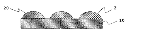
図1aから図1iは、本発明によるコンバータ・モジュール100の様々な実施形態を断面で概略的に示しており、これは以下で光コンバータ・システム100として示される。図1aに示されるシステム100は、コンバータ1、以下で光学素子2と呼ばれる光学部品2、金属リング3、および好ましくは金属リング3の外部上に与えられる層4から成る。光学素子2は、コンバータ1の頂面1a上に配置される。光学素子2およびコンバータ1は、互いに粘着性を持って接合される。光学素子2の頂面2aまたは光学素子2は、少なくとも部分的にまたは完全に凸レンズ2を形成する。例えば、凸レンズは基本的に半球の形状を有する。このようにして、コンバータ1から放出された光は、導くことができ、具体的には焦点に集めることができる。金属リング3は、光学素子2の周囲の広がりの上に十分に及ぶ。リング3は、基本的にはシステム100に対する支持具として、ならびに/あるいは例えば容器200の熱の引出しおよび/または位置決め支援および/または固定手段として働く。層4またはクラッディング4は、現在リング3の外側に与えられる。層4は、例えばクラッディング4として、具体的には堆積法によって形成することができる。層4は、基本的に、防食および/または容器200への接続の改善に役立つ。ここで図12aから図に12dに関する所見を参照する。
FIGS. 1 a to 1 i schematically show in cross-section various embodiments of a
図1bから図1iに示された個々の実施形態は、図1aに示された実施形態に部分的に対応する。同一の構成要素に関して、繰返しを避けるために、上記で示された図1aに関する説明を参照する。以下の所見は、基本的に差異に言及する。 The individual embodiments shown in FIGS. 1b to 1i partially correspond to the embodiment shown in FIG. 1a. For the same components, to avoid repetition, reference is made to the description relating to FIG. 1a shown above. The following observations basically refer to differences.
図1bは、コンバータ1が、2段の、または少なくとも2段のコンバータ・システム1として設計されている実施形態を示す。多段システムも、サンドイッチ構造で示すことができる。ここで、具体的には、蛍光体層などの異なるコンバータ層11および12は、例えばコンバータ1へと組み合わせることができる。2つの異なるコンバータ1の実施例には、Ce:YAGコンバータ11および赤色蛍光体コンバータ12がある。
FIG. 1 b shows an embodiment in which the
図1cは、コンバータ1が、2段の、または少なくとも2段のシステム11および13として具現化されている実施形態を示す。特に1つの層13の中の、目標とされた散乱中心および/またはディフューザ中心が、ここで作製されることになる。そのような2段システムの一実施例は、Ce:YAGコンバータ11および好ましくは白色YAG層13である。
FIG. 1 c shows an embodiment in which the
この2段システムは、本発明による光コンバータ・システム100の用途次第で、リング3を装備してもしなくてもよい。図1dは、光コンバータ・システム100のこの実施形態を示し、これはコンバータ1および光学素子2のみから成る。
This two-stage system may or may not be equipped with a
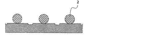
図1eは、光学素子2が、複数のより小さな光学素子2から構成される実施形態を示す。図1dに示される大きな凸レンズ2は、現在複数の小さな凸レンズ2と交換または置換され、それらはコンバータ1の頂面1a上に配置される。これによって、光学素子2の光学的性質を同等に保ちつつ光学素子2の高さを縮小することができる。
FIG. 1 e shows an embodiment in which the
本発明による光コンバータ・システム100は、必ずしも平面状のシステム100としてのみ設計されるわけではない。このことは、具体的には図1fに示された構成からも見られる。コンバータ層1またはコンバータ1は、平面状ではない。コンバータ1は、湾曲して、もしくは部分的に湾曲して設計される。光学素子2も、湾曲して、もしくは部分的に湾曲して形成される。
The
図1gは、光学素子2の頂面2aが、いわゆるDOE(「回折光学部品」)2として形成される実施形態を示す。DOE 2の一実施例にフレネルレンズがある。これは簡単な形状で示される。また、任意選択のコーティング14または機能層14が、コンバータ1の底面1b上に与えられる。そのような機能層14の例示的実施形態は、好ましくは光コンバータ・システム100の光のデカップリング効率を向上するための反射防止層14である。例えば、青色LED 260に対してコンバータ1の屈折率をここで一致させることができる。
FIG. 1 g shows an embodiment in which the
代替形態として、あるいはそれに加えて、光のデカップリング効率の向上は、コンバータ1の屈折率と光学素子2の屈折率との間の一致によって達成することができる。例えば、コンバータ1は1.8の屈折率を有することができる。例えば、P−LASF 47などの低いTgを有するガラスは、光学素子2に対する1.8の一致した屈折率を有する。
As an alternative or in addition, an increase in the light decoupling efficiency can be achieved by matching between the refractive index of the
図1hは、凸レンズなどの別の光学素子21が、コンバータ1の底面1b上に配置され、もしくは与えられる実施形態を示す。LED 260から来る光ビームは、次いで、この追加の光学素子21によって束ねられ得る。これは、その結果としてデカップリング効率の改善をもたらす。
FIG. 1 h shows an embodiment in which another
図1iは、熱を引き出すための手段5がコンバータ1の頂面1a上に配置され、もしくは与えられる実施形態を示す。熱を引き出すための手段5は、例えば、金属層またはダイヤモンド層で作製されたグリッドまたは網状組織である。手段5は、金属リング3に結合され、もしくは与えられる。これは熱放出の改善をもたらす。
FIG. 1 i shows an embodiment in which the
コンバータ1は、好ましくは無機のコンバータ1であり、あるいは無機材料を含む。無機コンバータ1用の材料の実施例は、ガラス・セラミックスもしくはガラス・セラミックスを含むもの、PiG(ガラス中の蛍光体)および/またはセラミックス化ガラスである。前述のように、リング3は、好ましくは金属リング3である。金属リング3用の材料の実施例は、NiFeCo合金もしくはNiFeCo合金を含むもの、NiFe合金および/または好ましくはフェライト含有特殊鋼である。光学素子の材料またはガラスは、好ましくはコンバータの特性に一致する。ガラスは、約1.4から約2の範囲の屈折率を有する。光学素子2用の適切な材料またはガラスは、高いIR透過率を有するガラス(熱放射を透過するため)、および/または相対するコンバータ1および金属リング3のストレスを低減するために熱膨張率(CTE)が一致するガラス、および/またはデカップリング効率を向上するために屈折率がコンバータ1と一致する透明ガラス、および/または基本的にコンバータ1のTg未満の低いTgを有するガラスであり得る。好ましくは、ガラスのTgは、コンバータ1のTg未満の約50℃から約300℃に存在する。適切なガラスは、例えばショットのガラス8250、T−SK57、T−LASF47などの低いTgを有するガラスである。不適当なガラスは、例えばP−SF67であり、色変化および/または不透明化が生じる恐れがあるからである。コーティング4の適用または堆積は、以下の図には示されていない。そのようなコーティング4の一実施例は、電気めっき4である。具体的な実施は、SnAgCuはんだである。コーティング4を金属リング3上に与えるには、多くの場合金属リング3の前処理が必要である。前処理の一実施例は、エッチング・プロセスである。これは、例えばHFおよび/またはHC1酸によって実行することができる。したがって、好ましい実施形態では、本発明による光コンバータ・システム100は、無機の光コンバータ・システム100である。
The
本発明による光コンバータ・システム100は、個々に作製することができる。しかし、複数の光コンバータ・システム100を同時に作製するのが好ましい。この目的に必要な構成要素1、2、3および/または4は、それぞれ一種のマトリックス40またはアレイ40またはライン40内に、少なくとも部分的に配置され、もしくは設けられる。マトリックス40は、好ましくは約50から約20,000の位置を含むことができる。図2aから図11dは、本発明による光コンバータ・システム100を作製する様々な方法の実施形態を概略的に示す。この製造はマトリックス40の中で毎回行なわれる。これに必要な構成要素が断面で示されている。
The
図2aから図2fは、本発明による方法の第1の例示的実施形態を示す。最初に支持体40が設けられ、その頂面に複数の凹部41が導入される(図2a)。複数の凹部41が導入されるので、支持体40はアレイ40としても示される。支持体40は、好ましくは調整された黒鉛鋳型である。後続の方法ステップで、次に、コンバータ1またはコンバータ・プレート1が、支持体40の頂面上に、または凹部41内に位置決めされる(図2b)。後続のステップで、次に金属リング3が、例えば簡単な配置によって支持体40の頂面上に位置決めされる(図2c)。光学素子2は、コンバータ1、リング3および/またはガラス・ゴブ2から形成され、これらの位置決めは、ここでいわゆるリミッタ50または障壁50によって支持され得る(図2d)。これらの障壁50は、一方では溶解する障壁として働き、その結果、以下の方法ステップで導入されるガラス・ブランク2を画定されたやり方で溶解することができる。障壁50は、センタリング補助具としても使用することができ、したがって調節ピン50としても示され得る。障壁50は、例えば、好ましくは黒鉛プレート50であるプレート50として設けることができ、支持体40の頂面の上に直接位置決めされる。後続の方法ステップで、ガラス部分2としても示されるガラス・ゴブ2は、支持体40の頂面上に、詳細にはコンバータ1上に位置決めされる(図2e)。ガラス・ゴブ2は、例えば「ピック・アンド・プレイス」などの実装プロセスによっても位置決めされる。ガラス・ゴブ2は、例えばビードおよび/またはロッド形セグメントとして設けることができる。次のステップで、ガラス・ゴブ2が溶解される(図2f)。このために、ガラス・ゴブ2は約600℃から約1000℃の温度に加熱される。ガラス部分2が低粘度になって流れる。各場合で、ガラス・ゴブ2は金属リング3およびコンバータ1に接合される。これは結合力のある接続である。障壁50および/またはリング3が、ガラス・ゴブ2の崩壊または液化のための境界を形成し、その結果、表面張力に基づいて、基本的に画定された凸レンズが光学素子2として形成される。これは、特に約104dPasから106dPasの範囲の粘度で起きる。一般に、溶解は約1分から15分の期間で起きる。溶解の期間中、光学素子2の形成およびコンバータ1と光学素子2との接合は、基本的に同時に起きる。
Figures 2a to 2f show a first exemplary embodiment of the method according to the invention. First, the
続いて、個々の光コンバータ・システム100が検査される。この後、次いで、それらは対応する容器200の中に組み込まれる。しかし、ここで図12aから図12dに関する所見を参照する。個々の光コンバータ・システム100の分離または支持体40からの除去は、図には示されていない。本実施例における構成要素100は、支持体40の凹部41の中または支持体の頂面上に実装または配置されているだけであるため、これらは簡単に除去することができる。しかし、光コンバータ・システム100は、必ずしも除去されない。複数の形成された光コンバータ・システム100も、マトリックスで顧客に供給され得る。
Subsequently, the individual
光学素子2の特性に対する悪影響を少なくとも低減するために、溶解の期間中、定義された雰囲気の中で溶解を実行することができる。そのような定義された雰囲気の実施例は、窒素および/または水素および/またはアルゴンである。ここではガラス光学素子に関して光学素子2のガラス面を改善するために、光学素子2の頂面2a上で火造りをさらに行なうことができる。
In order to at least reduce the adverse effects on the properties of the
図3aおよび図3bは、上記に示された方法の変形形態を示す。コンバータ1ならびに付属の金属リング3の両方が凹部41の中に配置されるように、支持体40の頂面の凹部41を構成する方法が説明される。コンバータ1および金属リング3の両方が、好ましくは「ピック・アンド・プレイス・プロセス」によって位置決めされる。これは、金属リング3が支持体40の表面上に見いだされてコンバータ1が凹部41の中に見いだされる図2cおよび図2dとは異なる。もちろん、コンバータ1および金属リング3の両方が支持体40の表面上に位置決めされることも考えられる。そのような場合、前述の障壁50によって位置決めを達成することができる。また、コンバータ1は、より小さなコンバータ・ユニット1から組み合わせられて存在する。個々のコンバータ・ユニット1は、光学素子2との合成物を溶解することによってコンバータ1へと組み合わせられる。
3a and 3b show a variation of the method shown above. A method of configuring the
図3cおよび図3dは、金属フレーム3だけが支持体40の頂面上に位置決めされる、方法の別の変形形態を示す。ガラス部分2が位置決めされ、ガラス部分2の溶解は金属フレーム3の中で実行される。形成された合成物が、支持体40から取り出される。この後、形成された光学素子2の裏面2bは平面状に削られ、かつ/または研磨される。続いて、この合成物は、光学素子2の裏面2bを削ることによってコンバータ1に接合される。コンバータ1への、ここではコンバータ1の前面1aへの合成物の接合は、コンバータ1を、光学素子2または合成物の処理された裏面2b上へ、結合、圧縮、焼結、分配および/または積層することによって実行される。
FIGS. 3 c and 3 d show another variant of the method in which only the
本発明による方法の別の実施形態が、図4aから図4dで説明される。ガラス・プレート20とコンバータ1またはコンバータ・プレート10とは、最初のステップで互いに向き合って位置決めされる(図4a)。ガラス・プレート20の焼結が、コンバータ・プレート10上で実行される(図4b)。これは、ガラス・プレート20のガラスのTgの直ぐ上の温度で行なわれる。その結果、ガラス・プレートの構造が存在する(図4c)。構造化は、凹部22または流路22がガラス・プレート20の中に形成されるように行なわれる。この場合、個々のガラス・ゴブ2がコンバータ・プレート10の頂面上に形成され、これらから光学素子2が後に形成される。構造化は、RIE(「リアクティブ・イオン・エッチング」)および/またはサンドブラストおよび/またはウェット・エッチングおよび/または超音波加工および/または切断によって行なうことができる。構造化は、好ましくはリソグラフィ法によって行なわれる。具体的にはRIEによる構造化の場合、一般に、ガラス・プレート20の頂面20a上に一種のマスクが与えられ、次いで構造化の後に再び除去されるが、これは本図には示されてない。構造化の後、ガラス部分2の溶解が行なわれる(図4d)。ガラスの画定された溶解では、いわゆる半球面レンズが光学素子2として形成される。ガラスは、ガラスのTgより高い約100℃から140℃の温度範囲、好ましくは約120℃で溶かされる。この場合、625℃の温度が、ガラスT−SK57向けにもたらされる。溶解する期間は、約15分から約25分の範囲内にあり、好ましくは約20分である。光コンバータ・システム100は、例えば切断またはラッピングによって分離される。その分だけ大きな構成要素が必要な場合、光コンバータ・システム100を直接用いることもできる。
Another embodiment of the method according to the invention is illustrated in FIGS. 4a to 4d. The
図5aから図5dは、ガラス・プレート20が構成されるプロセスの変形形態を示す。この場合、支持体40が設けられ、これに凹部41が導入され、コンバータ・プレート1またはコンバータ1を凹部41の中に位置決めすることができる(図5a)。コンバータ1上および好ましくは支持体40上へのガラス・プレート20の焼結(図5b)、ガラス・プレート20の構造化(図5c)、および構造化によって形成されたガラス・ゴブ2の溶解(図5d)が、すべて実行される(図5d)。さらなる詳細については、図4aから図4dに関する実施形態が参照される。ここで光学素子2が形成されるが、画定されたやり方で行なわれ、というのは、コンバータ1の縁端部または凹部41によるガラス・ゴブ2の崩壊に対して一種の障壁50が形成されるからである。
Figures 5a to 5d show a variation of the process in which the
図6aから図6dは、本発明による方法の次の実施形態を示す。最初に、コンバータ・プレート10が設けられる(図6a)。コンバータ・プレート10には、固定50または障壁50およびガラス・ゴブ2が備わっている(図6bまたは図6c)。ガラス・ゴブ2は、例えばガラス・ビード2として設けることができる。ガラス・ブランク2を溶解するための障壁が、障壁50によって画定される。障壁50は、好ましくは黒鉛から形成される。溶解は図6dに示されている。この溶解は、図5dに示された溶解と同様に行なわれる。
Figures 6a to 6d show the next embodiment of the method according to the invention. Initially, a
図7aから図7dは、図6aから図6dに示された方法の変更形態を示す。この場合、コンバータ1またはコンバータ・プレート10の頂面10aの構造15による溶解のために、障壁50または境界50が形成または画定される。この場合、障壁50または構造50は、凹部15などの引き去った構造15、または与えられた層15などの加えた構造、あるいはこれら2つの組合せによって設けることができる。構造50は、例えば、コンバータ・プレート10の頂面10aの凹部15または開口15として、現在形成されている。この構造は、例えば焼結、RIE、切断および/またはコーティング/リソグラフィ・プロセスによって作製される。障壁50は、好ましくはコンバータ1の頂面1aに障壁50を設けること、および構造化することの組合せによっても作製することができる。
Figures 7a to 7d show a modification of the method shown in Figures 6a to 6d. In this case, a
本発明による方法の別の実施形態が、図8aから図8hに示されている。最初に、好ましくは黒鉛鋳型である型60が設けられる(図8a)。型60の片側面に、複数の凹部61が導入される。型および個々の凹部61または開口61の寸法は、形成される光コンバータ・システム100に適合される。凹部61は、この場合光学素子2である形成されることになる光コンバータ・システム100のための雌型を表す。所望のレンズ効果をもたらすために、レンズ形状は、黒鉛鋳型61または開口61の幾何形状によって調節される。光学素子2は、いわゆるブランク・プレス・プロセスによって設けられる。型60は、その開口61内にガラス・ゴブ2を備える(図8b)。好ましくは黒鉛鋳型として形成された第2の上型70によって、ガラス・ゴブ2は、次に下型60と上型70との間でブランク・プレスされる(図8cおよび図8d)。これは、好ましくはガラスのTgを約50℃から約90℃上回る範囲の温度で行なわれる。
Another embodiment of the method according to the invention is shown in FIGS. 8a to 8h. Initially, a
1つまたは複数のコンバータ1の供給が、図8eから図8gで説明される。最初に型80が設けられる。対応する開口81が、型80の頂面に導入される。開口81は、型および形成されることになる光コンバータ・システム100またはコンバータ1の寸法に適合される。開口81は、形成されることになる光コンバータ・システム100、特にコンバータ1の雌型を示す。一種のチャンネル82が、それぞれの開口81の頂面に任意選択で導入される。コンバータ1は、このチャンネル82によって位置決めされる。コンバータ1は、作製されることになる色座標の安定性により、好ましくは一定の厚さを有する。次にコンバータ1が加熱される。加熱は、約400℃から800℃の範囲の温度で行なわれる。コンバータ1は、崩壊し、開口81の中へ沈下して、基本的に開口81の形状に一致する。
The supply of one or
2つのあらかじめ成形された構成要素、光学素子2およびコンバータ1の組合せが図8hに示されている。2つの構成要素1および2は、例えばゾル−ゲル接合および/または拡散接合などの接続プロセスによって互いに接合される。
The combination of two preformed components,
前述の弛みおよび沈下のプロセスの変形形態が、図9aから図9cに示されている。最初に、図8eから図8gに既に示された形状のコンバータ・プレート1が設けられて加熱される(図9a)。コンバータ1が成形または形成された後、次に、光学素子2、好ましくはレンズ2がリフロー・プロセスによって与えられる。これは図9bおよび図9cに示されている。最初に、現在小さなビードとして形成されているガラス・ゴブ2が、開口81の中に設けられる。個々のコンバータ1とそれぞれのガラス・ゴブ2との接合は、ガラス・ゴブ2を加熱して溶解することにより行なわれる。レンズ2または光学素子2は、同時に形成または成形される。
A variation of the aforementioned slack and settlement process is shown in FIGS. 9a to 9c. First, a
図10aから図10dは、本発明による方法の別の変形形態を示す。この場合、光コンバータ・システム100は、ブランク・プレス・プロセスによって作製される。このために、ガラス・ゴブ2およびコンバータ1の両方が、それぞれ型60の開口61の中に設けられる。光コンバータ・システム100の形成または光コンバータ・システム100の構成の形成は、型70と型60とを組み合わせることにより、ここで作製される。光学素子2の中にDOE構造体23または微細光学素子の構造体23をさらに導入するために、詳細には光学素子2の頂面2aにそれを導入するために、対応する構造体62が開口61の底部に導入または配置される。示されたジグザグ形状は、対応する構造体を示す。構造体62は、光学素子2の頂面2aの上に形成される構造体23の雌型を示す。したがって、熱間プレスには、圧縮型60および70、コンバータ基板1、および低いTgを有するガラスで作製されたガラス・ゴブ2がさらに備わっている。構造体62は、いわばガラスまたは光学素子2の中に加えられる。以下の方法パラメータが、ガラスP−SK57向けにもたらされる。圧縮は、530℃から590℃、好ましくは約560℃の温度、約10から50kg/cm2で、特に約1分から3分間行なわれる。
Figures 10a to 10d show another variant of the method according to the invention. In this case, the
もちろん、金属リング3が個々の図に詳細に示されていなくても、前述の方法で作製された光コンバータ・システム100は、金属リング3を装備しても装備しなくてもよい。金属リング3が使用される場合、金属リング3も、もちろん金属化することができる。このために、図11aから図11dは、図10aから図10dで説明された金属リング3を使用する方法をもう一度示す。金属リング3は、例えば型70によって設けられる。それらの金属リング3は、形成された空間に位置決めすることもできる。
Of course, even if the
図12aから図12dは、本発明による光コンバータ・システム100のパッケージ200または容器200内での使用を示す。トータル・システム300またはLEDパッケージ300が形成される。本発明による光コンバータ・システム200は、容器200用のいわば一種のカバーとして働く。パッケージ200は、GTMS(「ガラス金属封じ」)パッケージ、Siパッケージ、プラスチック・パッケージ、および/または、セラミックス・パッケージであり得る。
12a to 12d illustrate the use of the
図12aおよび図12dは、容器200の断面を示す。それぞれの場合で、これは3層容器200である。3層容器200は、ベース部分201、第1のガラス層202、2つの接続部分203、第2のガラス層204およびヘッド部分205で作製された合成物から成り、あるいはこれを備える。LED 260は、容器200の内部に配置される。LED 260またはLEDチップ260は、実装領域212に配置される。LED 260は、ワイヤ273によって接続部分203および204に接合される。LED 260から放出される放射または光に対するいわゆる通過領域261が、LED 260の上に見いだされる。通過領域261の頂面は、本発明による光コンバータ・システム100によって封止される。通過領域261は、したがってパッケージ200も、カバー100によって好ましくは密閉封止される。これは、光コンバータ・システム100を、金属から設けられるヘッド部分205または容器200の頂面200aへ例えばはんだ付けすることによって行なうことができる。
12a and 12d show a cross section of the
例えば、LED 260は青色発光LEDであり、コンバータ1はいわゆる黄リンなどの発光色物質を含むガラスである。波長の短い青色光は、発色剤を励起して発光させる。この効果は光ルミネッセンスと呼ばれる。このようにして、波長の長い黄色光が放出される。一般に、青色光の全体が変換されるわけではない。このようにして、青色と黄色との2つのスペクトル色の加法混色から白色光がもたらされる。青色から黄色への変換は、セラミックス化ガラスによっても行なわれ得る。別の実施例では、LED 260はUV光を放出するLEDであり、コンバータ1は、いわゆる赤、緑および青(RGB)の燐などのいくつかの発光する発色物質を含むガラスである。波長の短いUV光は、発色剤を励起して発光させる。赤色光、緑色光および青色光は、このようにして放出される。したがって、白色光は加法混色からもたらされる。CRI値を向上させるために、コンバータ1は、RGB−LED 260と組み合わせることもできる。それぞれの場合において、任意選択で少なくとも1つの赤色LED 260および/または1つの緑色のLED 260をさらに使用することができるが、図には示されていない。このようにして色の位置を変化させることができ、光は細かく調整することができる。
For example, the
図12aは、システム100が「単に」容器200上に配置された実施形態を示す。LED 260の上に示された3つの矢印は、LED 260によって放出された放射の放出方向を示す。図12bは、コンセントレータ24またはいわゆる「光導波路」24が、光学素子2としてコンバータ1上に配置される実施形態を示す。一方では、コンセントレータ24の内側は反射器として働く。他方では、内壁は、コンバータ1から水平方向に放出された光に対する一種の光ガイドとしても動作する。システム300全体のデカップリング効率が、コンセントレータ24によって向上され得る。また、レンズ25として設計された第2の光学素子2が、コンセントレータ23上に配置される。
FIG. 12 a shows an embodiment in which the
また、別の光学素子21を、コンバータ1の下に配置することができ、好ましくはコンバータ1の底面1b上に直接配置することができる。LED 260から来る光またはLED 260から来る放射光のバンドリングは、そのような光学素子21によってもたらされ得る。これは図12cに示されている。
Further, another
図12aから図12cは、それぞれの場合に、システム100がLED 260から離れて配置される本発明の適用例を示す。図12dは、コンバータ1が、LED 260上にある、もしくはLED 260に隣接して位置決めされる実施形態を示す。通過領域261は、この場合、基本的にコンバータ1によって完全に埋め尽くされる。
Figures 12a to 12c show an application of the present invention in which the
本システム100は、好ましくは無機のシステム100である。システム100は、好ましくは、少なくとも1つのコンバータ1および/または光学素子2および/または金属サポート3から成る。金属サポート3は、前述のようにリング3またはキャップ3として形成することができる。システム100は、とりわけパッケージ・カバーまたはパッケージ封止として使用することができる。この方法の設計は大量生産に適切である。溶解、弛み、焼結、スタンピングなどの普及しているプロセスに基づいて、これが可能である。本発明による光コンバータ・システム100は、耐温度性だけでなく温度変化に対する抵抗も、明らかに既知のシステムのものに優る。システム100に関して、金属リング3なしで約400℃までの耐温度性を得ることができる。金属リング3および、例えばSn含有はんだに関して、システム100は約350℃までの耐温度性を有する。また、システムの好ましい構成要素は、UVおよび化学物質に対して耐性があり、もしくは実質的に耐性がある。本発明によるシステム100がパッケージ・カバーとして使用される場合、システム100は、空気および/または湿気に対して封止するやり方でパッケージ200上に固定され得る。好ましくは基本的に無機構成要素だけが使用されるので、構成要素の、例えば炭化水素の形態での脱気はない。したがって、LED 260の有機的汚染を基本的に回避することができる。パッケージ200は加熱乾燥することができ、実際、不活性ガスを充填して封止することができる。
The
説明された実施形態が一例として理解されるべきであることは、当業者にとって明白である。本発明はこれらの実施形態に限定されず、本発明の趣旨から離れることなく多くのやり方で本発明を変化させることができる。個々の実施形態の特徴および各場合で説明の一般部で挙げられた特徴は、それら自体の間で組み合わせることができ、互いに組み合わせることもできる。 It will be apparent to those skilled in the art that the described embodiments are to be understood as examples. The invention is not limited to these embodiments, and the invention can be varied in many ways without departing from the spirit of the invention. The features of the individual embodiments and the features listed in the general part of the description in each case can be combined between themselves or can be combined with each other.
1 コンバータ
1a コンバータの頂面
1b コンバータの底面
2 光学部品または光学素子またはガラス・ゴブまたはガラス部分
2a 光学部品の頂面
2b 光学部品の底面
3 リングまたは金属リングまたは金属サポート
4 コーティングまたはクラッディング
5 熱除去のための手段
10 コンバータ・プレート
10a コンバータ・プレートの頂面
10b コンバータ・プレートの底面
11 コンバータ層
12 コンバータ層
13 コンバータ層
14 機能層またはコーティング
15 構造または開口または凹部
20 ガラス・プレート
20a ガラス・プレートの頂面
20b ガラス・プレートの底面
21 光学部品または光学素子
22 凹部または流路
23 DOE構造体または微細構造
24 コンセントレータ
25 レンズ
40 マトリックスまたはアレイまたは支持体
41 凹部
50 境界またはリミッタまたは障壁
60 下型または支持体
61 凹部または開口
62 構造体
70 上型
71 凹部61の対応部分
80 型または支持体
81 凹部または開口
82 チャンネル
100 コンバータ・モジュールまたは光コンバータ・システム
200 容器または機能要素の容器
200a 容器の頂面
201 ベース部分またはベースまたは支持体
202 第1のガラス層
203 接続部分または導体細長片
204 第2のガラス層
205 ヘッド部分または反射器
212 機能要素のための組立て領域
260 光電子機能要素またはLED
261 通過領域
273 ワイヤまたはワイヤ・ボンディング
300 トータル・システムまたはLEDパッケージ
DESCRIPTION OF
261
Claims (45)
放出された放射および/または前記受け取られる放射を変換するための、少なくとも1つの無機コンバータ(1)と、
無機材料を含み、光電子機能要素(260)の放出方向でコンバータ(1)に対して下流に配置された少なくとも1つの光学部品(2)とを備え、
コンバータ(1)と光学部品(2)とが、好ましくは結合力のあるやり方で互いに接合されるコンバータ・モジュール(100)。 Made by a method for radiation emitted from and / or received by at least one optoelectronic functional element (260), preferably radiation from an LED (260), or in particular according to one of the following claims A converter module (100) for placement on a possible or fabricated optoelectronic functional element (260) comprising:
At least one inorganic converter (1) for converting emitted radiation and / or said received radiation;
Comprising at least one optical component (2) comprising an inorganic material and arranged downstream relative to the converter (1) in the emission direction of the optoelectronic functional element (260),
Converter module (100) in which the converter (1) and the optical component (2) are joined together, preferably in a cohesive manner.
容器(200)の中に配置され、特にLED(260)である、放射線を発し、および/または放射線を受け取る少なくとも1つの光電子機能素子(260)とを備える光電子構成要素。 At least one container (200) and at least one converter module (100) according to any one of the preceding claims;
Optoelectronic component comprising at least one optoelectronic functional element (260) that emits radiation and / or receives radiation, which is arranged in a container (200), in particular an LED (260).
前記放出された放射および/または前記受け取られる放射を変換するための、少なくとも1つのコンバータ(1)を設けること、
少なくとも1つの光学部品(2)を設けること、
コンバータ(1)と光学部品(2)とが互いに付着して合成物を形成するように、コンバータ(1)および/または光学部品(2)を加熱するように、コンバータ(1)と光学部品(2)とを接合することを含む方法。 Converter according to any one of the preceding claims, for radiation emitted from and / or received by at least one optoelectronic functional element (260), preferably radiation from an LED (260) A method of making a module (100),
Providing at least one converter (1) for converting the emitted radiation and / or the received radiation;
Providing at least one optical component (2);
Converter (1) and optical component (2) are heated to heat converter (1) and / or optical component (2) such that converter (1) and optical component (2) adhere to each other to form a composite. And 2).
Applications Claiming Priority (3)
| Application Number | Priority Date | Filing Date | Title |
|---|---|---|---|
| DE102008021436.1 | 2008-04-29 | ||
| DE102008021436A DE102008021436A1 (en) | 2008-04-29 | 2008-04-29 | Optic converter system for (W) LEDs |
| PCT/EP2009/003108 WO2009132837A2 (en) | 2008-04-29 | 2009-04-29 | Optical converter system for (w)leds |
Publications (2)
| Publication Number | Publication Date |
|---|---|
| JP2011519173A true JP2011519173A (en) | 2011-06-30 |
| JP5959199B2 JP5959199B2 (en) | 2016-08-02 |
Family
ID=40984688
Family Applications (1)
| Application Number | Title | Priority Date | Filing Date |
|---|---|---|---|
| JP2011506606A Expired - Fee Related JP5959199B2 (en) | 2008-04-29 | 2009-04-29 | (W) Light converter system for LED |
Country Status (7)
| Country | Link |
|---|---|
| US (2) | US9409811B2 (en) |
| EP (1) | EP2272108B1 (en) |
| JP (1) | JP5959199B2 (en) |
| KR (1) | KR20110016903A (en) |
| CN (1) | CN102017201B (en) |
| DE (1) | DE102008021436A1 (en) |
| WO (1) | WO2009132837A2 (en) |
Cited By (2)
| Publication number | Priority date | Publication date | Assignee | Title |
|---|---|---|---|---|
| KR20200044219A (en) * | 2018-10-12 | 2020-04-29 | 장은석 | Method of Manufacturing Super-Slim LED Lens having High Transparency by using SLA type 3D Printing |
| JP2020518036A (en) * | 2017-04-24 | 2020-06-18 | ルミレッズ ホールディング ベーフェー | High brightness light conversion device |
Families Citing this family (27)
| Publication number | Priority date | Publication date | Assignee | Title |
|---|---|---|---|---|
| JPWO2010119934A1 (en) * | 2009-04-14 | 2012-10-22 | パナソニック株式会社 | Light emitting device, light characteristic adjusting method, and light emitting device manufacturing method |
| DE102010005169A1 (en) | 2009-12-21 | 2011-06-22 | OSRAM Opto Semiconductors GmbH, 93055 | Radiation-emitting semiconductor component |
| DE102010022561A1 (en) * | 2010-06-02 | 2011-12-08 | Osram Opto Semiconductors Gmbh | Wavelength conversion element, optoelectronic component with a wavelength conversion element and method for producing a wavelength conversion element |
| DE102010034923A1 (en) * | 2010-08-20 | 2012-02-23 | Osram Opto Semiconductors Gmbh | Process for the preparation of a composite layer of a luminescence conversion layer and a litter layer |
| DE102010035331B4 (en) * | 2010-08-24 | 2021-09-30 | Schott Ag | Process for the production of lens-shaped optical components from glass and reflow asphere |
| DE102010046122A1 (en) | 2010-09-21 | 2012-03-22 | Osram Opto Semiconductors Gmbh | Electronic component |
| DE102010049312B4 (en) | 2010-10-22 | 2023-08-03 | OSRAM Opto Semiconductors Gesellschaft mit beschränkter Haftung | Process for producing a conversion plate and conversion plate |
| DE102011009369A1 (en) * | 2011-01-25 | 2012-07-26 | Osram Opto Semiconductors Gmbh | Optoelectronic semiconductor chip and method for its production |
| DE102011003969B4 (en) * | 2011-02-11 | 2023-03-09 | OSRAM Opto Semiconductors Gesellschaft mit beschränkter Haftung | Process for producing an optoelectronic component |
| DE102011113777A1 (en) * | 2011-09-19 | 2013-03-21 | Osram Opto Semiconductors Gmbh | Wavelength conversion element and light-emitting semiconductor component with wavelength conversion element |
| US9444024B2 (en) * | 2011-11-10 | 2016-09-13 | Cree, Inc. | Methods of forming optical conversion material caps |
| DE102012005657B4 (en) * | 2012-03-22 | 2020-06-10 | Schott Ag | White light lighting device |
| DE102012109020A1 (en) * | 2012-09-25 | 2014-03-27 | Osram Opto Semiconductors Gmbh | Conversion element comprises support element having recess which extends from first major surface to second major surface of element, and conversion agent to convert primary radiation incident on conversion agent into secondary radiation |
| KR102120759B1 (en) | 2012-11-30 | 2020-06-09 | 엘지이노텍 주식회사 | Wafer level optics apparatus |
| DE202013101400U1 (en) * | 2013-04-02 | 2014-07-03 | Zumtobel Lighting Gmbh | Arrangement for converting the light emitted by an LED light source |
| EP2953176A1 (en) * | 2014-06-02 | 2015-12-09 | Swarovski Energy GmbH | Lighting device |
| DE102016224090B4 (en) * | 2016-12-05 | 2024-03-28 | OSRAM Opto Semiconductors Gesellschaft mit beschränkter Haftung | Optoelectronic component, module with at least two optoelectronic components and method for producing an optoelectronic component |
| DE102018111898B4 (en) | 2017-06-06 | 2025-10-16 | Schott Ag | Method for producing a housing for an optoelectronic component |
| DE102017123415A1 (en) * | 2017-10-09 | 2019-04-11 | Osram Opto Semiconductors Gmbh | Optoelectronic component and method for producing an optoelectronic component |
| EP3524135A1 (en) * | 2018-02-13 | 2019-08-14 | Essilor International (Compagnie Generale D'optique) | Wearable binocular optoelectronic device for measuring light sensitivity threshold of a user |
| JP6964050B2 (en) * | 2018-07-20 | 2021-11-10 | オリンパス株式会社 | Manufacturing method of optical element |
| CN113394320B (en) | 2020-03-11 | 2023-04-07 | 隆达电子股份有限公司 | Light emitting diode packaging structure |
| KR102310911B1 (en) * | 2020-11-12 | 2021-10-08 | 유버 주식회사 | Led luminescence apparatus |
| WO2022226725A1 (en) * | 2021-04-26 | 2022-11-03 | 京东方科技集团股份有限公司 | Optical module and manufacturing method therefor, and display apparatus |
| DE102022123050A1 (en) | 2022-09-09 | 2024-03-14 | Schott Ag | Lighting device |
| DE102022123051B4 (en) * | 2022-09-09 | 2024-10-17 | Schott Ag | lighting equipment |
| DE102023114878A1 (en) * | 2023-06-06 | 2024-12-12 | Grammer Aktiengesellschaft | Method for producing a glass component device for a fitting part of the vehicle interior and glass component device |
Citations (27)
| Publication number | Priority date | Publication date | Assignee | Title |
|---|---|---|---|---|
| JPH08335747A (en) * | 1995-06-07 | 1996-12-17 | Anritsu Corp | Light emitting device module and manufacturing method thereof |
| JPH1187778A (en) * | 1997-09-02 | 1999-03-30 | Toshiba Corp | Semiconductor light emitting element, semiconductor light emitting device and method for manufacturing the same |
| JP2000031548A (en) * | 1998-07-09 | 2000-01-28 | Stanley Electric Co Ltd | Surface mount type light emitting diode and method of manufacturing the same |
| JP2000512806A (en) * | 1996-06-26 | 2000-09-26 | シーメンス アクチエンゲゼルシヤフト | Phosphor conversion-semiconductor light emitting device with element |
| JP2001043728A (en) * | 1999-07-30 | 2001-02-16 | Fujitsu Takamisawa Component Ltd | Light emitting diode lighting system |
| JP2003110146A (en) * | 2001-07-26 | 2003-04-11 | Matsushita Electric Works Ltd | Light emitting device |
| WO2004082036A1 (en) * | 2003-03-10 | 2004-09-23 | Toyoda Gosei Co., Ltd. | Solid element device and method for manufacture thereof |
| JP2005039122A (en) * | 2003-07-17 | 2005-02-10 | Toyoda Gosei Co Ltd | Light emitting device |
| WO2005071039A1 (en) * | 2004-01-26 | 2005-08-04 | Kyocera Corporation | Wavelength converter, light-emitting device, wavelength converter manufacturing method, and light-emitting device manufacturing method |
| JP2005311170A (en) * | 2004-04-23 | 2005-11-04 | Stanley Electric Co Ltd | Semiconductor light emitting device |
| JP2006202962A (en) * | 2005-01-20 | 2006-08-03 | Toyoda Gosei Co Ltd | Light emitting device |
| WO2006087660A1 (en) * | 2005-02-17 | 2006-08-24 | Philips Intellectual Property & Standards Gmbh | Illumination system comprising a green-emitting ceramic luminescence converter |
| DE102005009066A1 (en) * | 2005-02-28 | 2006-09-07 | Osram Opto Semiconductors Gmbh | Method for producing an optical and a radiation-emitting component and optical and radiation-emitting component |
| JP2007005716A (en) * | 2005-06-27 | 2007-01-11 | Matsushita Electric Ind Co Ltd | Lens cap manufacturing method |
| JP2007013148A (en) * | 2005-06-30 | 2007-01-18 | Schott Ag | Solid state light source |
| JP2007035951A (en) * | 2005-07-27 | 2007-02-08 | Kyocera Corp | Light-emitting apparatus |
| JP2007031196A (en) * | 2005-07-26 | 2007-02-08 | Kyoto Univ | Phosphor and light emitting diode |
| JP2007088060A (en) * | 2005-09-20 | 2007-04-05 | Toshiba Lighting & Technology Corp | Light emitting device |
| JP2007103673A (en) * | 2005-10-04 | 2007-04-19 | Matsushita Electric Ind Co Ltd | Lid and manufacturing method thereof, and glass molded body manufacturing method |
| JP2007134656A (en) * | 2005-11-14 | 2007-05-31 | Toyoda Gosei Co Ltd | Phosphor plate and light emitting device having the same |
| JP2007273975A (en) * | 2006-03-10 | 2007-10-18 | Matsushita Electric Works Ltd | Light-emitting device |
| JP2007300043A (en) * | 2006-05-08 | 2007-11-15 | Asahi Rubber:Kk | Light emitting device |
| JP2008028352A (en) * | 2006-06-02 | 2008-02-07 | Nec Lighting Ltd | Electronic device and method for manufacturing electronic device |
| JP2008034546A (en) * | 2006-07-27 | 2008-02-14 | Nichia Chem Ind Ltd | Light emitting device |
| JP2008060428A (en) * | 2006-08-31 | 2008-03-13 | Nichia Chem Ind Ltd | Light emitting device and manufacturing method thereof |
| JP2008508742A (en) * | 2004-08-02 | 2008-03-21 | ゲルコアー リミテッド ライアビリティ カンパニー | White LED with adjustable color rendering index |
| JP2009535856A (en) * | 2006-05-03 | 2009-10-01 | スリーエム イノベイティブ プロパティズ カンパニー | Method for producing LED light extraction member array |
Family Cites Families (12)
| Publication number | Priority date | Publication date | Assignee | Title |
|---|---|---|---|---|
| DE19638667C2 (en) | 1996-09-20 | 2001-05-17 | Osram Opto Semiconductors Gmbh | Mixed-color light-emitting semiconductor component with luminescence conversion element |
| TW552726B (en) * | 2001-07-26 | 2003-09-11 | Matsushita Electric Works Ltd | Light emitting device in use of LED |
| JP2005298529A (en) * | 2001-12-28 | 2005-10-27 | Doppel:Kk | Highly photoluminescent material and method for producing the same |
| MY142684A (en) * | 2003-02-26 | 2010-12-31 | Cree Inc | Composite white light source and method for fabricating |
| EP1691425B1 (en) * | 2003-11-25 | 2010-08-11 | Panasonic Electric Works Co., Ltd. | Light emitting device using light emitting diode chip |
| US7791274B2 (en) * | 2004-01-07 | 2010-09-07 | Panasonic Corporation | LED lamp |
| US7361938B2 (en) * | 2004-06-03 | 2008-04-22 | Philips Lumileds Lighting Company Llc | Luminescent ceramic for a light emitting device |
| US7553683B2 (en) * | 2004-06-09 | 2009-06-30 | Philips Lumiled Lighting Co., Llc | Method of forming pre-fabricated wavelength converting elements for semiconductor light emitting devices |
| DE102004038727A1 (en) * | 2004-08-10 | 2006-02-23 | Schott Ag | Method and device for producing hybrid lenses |
| DE102005023134A1 (en) * | 2005-05-19 | 2006-11-23 | Patent-Treuhand-Gesellschaft für elektrische Glühlampen mbH | Luminescence conversion LED |
| JP5036222B2 (en) * | 2006-06-01 | 2012-09-26 | 京セラ株式会社 | Light emitting device |
| DE202007014397U1 (en) * | 2007-01-25 | 2008-01-03 | Schott Ag | Light-emitting device |
-
2008
- 2008-04-29 DE DE102008021436A patent/DE102008021436A1/en not_active Ceased
-
2009
- 2009-04-29 KR KR1020107026451A patent/KR20110016903A/en not_active Ceased
- 2009-04-29 JP JP2011506606A patent/JP5959199B2/en not_active Expired - Fee Related
- 2009-04-29 CN CN2009801154057A patent/CN102017201B/en not_active Expired - Fee Related
- 2009-04-29 EP EP09737881.4A patent/EP2272108B1/en not_active Not-in-force
- 2009-04-29 WO PCT/EP2009/003108 patent/WO2009132837A2/en not_active Ceased
- 2009-04-29 US US12/990,385 patent/US9409811B2/en not_active Expired - Fee Related
-
2016
- 2016-06-27 US US15/194,077 patent/US20160380161A1/en not_active Abandoned
Patent Citations (27)
| Publication number | Priority date | Publication date | Assignee | Title |
|---|---|---|---|---|
| JPH08335747A (en) * | 1995-06-07 | 1996-12-17 | Anritsu Corp | Light emitting device module and manufacturing method thereof |
| JP2000512806A (en) * | 1996-06-26 | 2000-09-26 | シーメンス アクチエンゲゼルシヤフト | Phosphor conversion-semiconductor light emitting device with element |
| JPH1187778A (en) * | 1997-09-02 | 1999-03-30 | Toshiba Corp | Semiconductor light emitting element, semiconductor light emitting device and method for manufacturing the same |
| JP2000031548A (en) * | 1998-07-09 | 2000-01-28 | Stanley Electric Co Ltd | Surface mount type light emitting diode and method of manufacturing the same |
| JP2001043728A (en) * | 1999-07-30 | 2001-02-16 | Fujitsu Takamisawa Component Ltd | Light emitting diode lighting system |
| JP2003110146A (en) * | 2001-07-26 | 2003-04-11 | Matsushita Electric Works Ltd | Light emitting device |
| WO2004082036A1 (en) * | 2003-03-10 | 2004-09-23 | Toyoda Gosei Co., Ltd. | Solid element device and method for manufacture thereof |
| JP2005039122A (en) * | 2003-07-17 | 2005-02-10 | Toyoda Gosei Co Ltd | Light emitting device |
| WO2005071039A1 (en) * | 2004-01-26 | 2005-08-04 | Kyocera Corporation | Wavelength converter, light-emitting device, wavelength converter manufacturing method, and light-emitting device manufacturing method |
| JP2005311170A (en) * | 2004-04-23 | 2005-11-04 | Stanley Electric Co Ltd | Semiconductor light emitting device |
| JP2008508742A (en) * | 2004-08-02 | 2008-03-21 | ゲルコアー リミテッド ライアビリティ カンパニー | White LED with adjustable color rendering index |
| JP2006202962A (en) * | 2005-01-20 | 2006-08-03 | Toyoda Gosei Co Ltd | Light emitting device |
| WO2006087660A1 (en) * | 2005-02-17 | 2006-08-24 | Philips Intellectual Property & Standards Gmbh | Illumination system comprising a green-emitting ceramic luminescence converter |
| DE102005009066A1 (en) * | 2005-02-28 | 2006-09-07 | Osram Opto Semiconductors Gmbh | Method for producing an optical and a radiation-emitting component and optical and radiation-emitting component |
| JP2007005716A (en) * | 2005-06-27 | 2007-01-11 | Matsushita Electric Ind Co Ltd | Lens cap manufacturing method |
| JP2007013148A (en) * | 2005-06-30 | 2007-01-18 | Schott Ag | Solid state light source |
| JP2007031196A (en) * | 2005-07-26 | 2007-02-08 | Kyoto Univ | Phosphor and light emitting diode |
| JP2007035951A (en) * | 2005-07-27 | 2007-02-08 | Kyocera Corp | Light-emitting apparatus |
| JP2007088060A (en) * | 2005-09-20 | 2007-04-05 | Toshiba Lighting & Technology Corp | Light emitting device |
| JP2007103673A (en) * | 2005-10-04 | 2007-04-19 | Matsushita Electric Ind Co Ltd | Lid and manufacturing method thereof, and glass molded body manufacturing method |
| JP2007134656A (en) * | 2005-11-14 | 2007-05-31 | Toyoda Gosei Co Ltd | Phosphor plate and light emitting device having the same |
| JP2007273975A (en) * | 2006-03-10 | 2007-10-18 | Matsushita Electric Works Ltd | Light-emitting device |
| JP2009535856A (en) * | 2006-05-03 | 2009-10-01 | スリーエム イノベイティブ プロパティズ カンパニー | Method for producing LED light extraction member array |
| JP2007300043A (en) * | 2006-05-08 | 2007-11-15 | Asahi Rubber:Kk | Light emitting device |
| JP2008028352A (en) * | 2006-06-02 | 2008-02-07 | Nec Lighting Ltd | Electronic device and method for manufacturing electronic device |
| JP2008034546A (en) * | 2006-07-27 | 2008-02-14 | Nichia Chem Ind Ltd | Light emitting device |
| JP2008060428A (en) * | 2006-08-31 | 2008-03-13 | Nichia Chem Ind Ltd | Light emitting device and manufacturing method thereof |
Cited By (4)
| Publication number | Priority date | Publication date | Assignee | Title |
|---|---|---|---|---|
| JP2020518036A (en) * | 2017-04-24 | 2020-06-18 | ルミレッズ ホールディング ベーフェー | High brightness light conversion device |
| JP7154280B2 (en) | 2017-04-24 | 2022-10-17 | ルミレッズ ホールディング ベーフェー | High brightness light conversion device |
| KR20200044219A (en) * | 2018-10-12 | 2020-04-29 | 장은석 | Method of Manufacturing Super-Slim LED Lens having High Transparency by using SLA type 3D Printing |
| KR102189950B1 (en) * | 2018-10-12 | 2020-12-11 | 장은석 | Method of Manufacturing Super-Slim LED Lens having High Transparency by using SLA type 3D Printing |
Also Published As
| Publication number | Publication date |
|---|---|
| KR20110016903A (en) | 2011-02-18 |
| US9409811B2 (en) | 2016-08-09 |
| US20110205740A1 (en) | 2011-08-25 |
| CN102017201B (en) | 2013-08-14 |
| US20160380161A1 (en) | 2016-12-29 |
| EP2272108B1 (en) | 2018-11-28 |
| CN102017201A (en) | 2011-04-13 |
| WO2009132837A2 (en) | 2009-11-05 |
| JP5959199B2 (en) | 2016-08-02 |
| EP2272108A2 (en) | 2011-01-12 |
| WO2009132837A3 (en) | 2009-12-23 |
| DE102008021436A1 (en) | 2010-05-20 |
Similar Documents
| Publication | Publication Date | Title |
|---|---|---|
| JP5959199B2 (en) | (W) Light converter system for LED | |
| CN102598288B (en) | For the manufacture of the method for the layout of the structural detail with on carrier substrate and layout and for the manufacture of process of semi-finished and semi-finished product | |
| US10647915B2 (en) | Converter for generating a secondary light from a primary light, light-emitting elements which contains such a converter, and method for producing the converter and the light-emitting elements | |
| EP2033232B1 (en) | Lighting device and manufacturing process thereof | |
| US8890401B2 (en) | Solid-state luminescent filament lamps | |
| EP3355368B1 (en) | Beveled chip reflector for chip-scale packaging light-emitting device and manufacturing method of the same | |
| JP5339728B2 (en) | Lighting device | |
| JP4979299B2 (en) | Optical device and manufacturing method thereof | |
| CN103688378B (en) | Optical element, opto-electronic device and their manufacture method | |
| CN102017202B (en) | Housing and its production method, base body, optoelectronic component and lighting device | |
| CN108365075B (en) | Wafer-level packaged light-emitting device with beveled wafer reflective structure and manufacturing method thereof | |
| JP2011188001A (en) | Optical preforming of solid-state light-emitting die, and manufacturing method therefor, assembly method, and system | |
| TW201011953A (en) | Phosphor layer arrangement for use with light emitting diodes | |
| JP2012523678A (en) | Power LED heat dissipation substrate, method for manufacturing power LED product, and product by the method | |
| JP2010177375A (en) | Light-emitting device and manufacturing method of the same | |
| TWI279598B (en) | Optical component and method of manufacturing the same | |
| CN103985807B (en) | Inorganic substrate and manufacture method thereof | |
| KR102045794B1 (en) | Beveled chip reflector for chip-scale packaging light-emitting device and manufacturing method of the same | |
| JP2019201089A (en) | Oblique angle chip reflector of chip scale packaging light emission device and manufacturing method of the same | |
| CN101308892A (en) | Light emitting diode packaging manufacturing method | |
| JP5144578B2 (en) | Method for manufacturing light emitting device | |
| US20200313057A1 (en) | High power led assembly and method of forming a high power led assembly | |
| KR20180000174A (en) | Phosphor plate and lighting device including the same | |
| KR100706958B1 (en) | Light-emitting device module using light-emitting device reflector and the reflector and manufacturing method thereof | |
| JP2019040996A (en) | Ultraviolet light element, package for ultraviolet light element, optical member used for ultraviolet light element, and method of manufacturing optical member |
Legal Events
| Date | Code | Title | Description |
|---|---|---|---|
| RD04 | Notification of resignation of power of attorney |
Free format text: JAPANESE INTERMEDIATE CODE: A7424 Effective date: 20120713 |
|
| A977 | Report on retrieval |
Free format text: JAPANESE INTERMEDIATE CODE: A971007 Effective date: 20120926 |
|
| A131 | Notification of reasons for refusal |
Free format text: JAPANESE INTERMEDIATE CODE: A131 Effective date: 20121002 |
|
| A601 | Written request for extension of time |
Free format text: JAPANESE INTERMEDIATE CODE: A601 Effective date: 20121228 |
|
| A602 | Written permission of extension of time |
Free format text: JAPANESE INTERMEDIATE CODE: A602 Effective date: 20130110 |
|
| A521 | Request for written amendment filed |
Free format text: JAPANESE INTERMEDIATE CODE: A523 Effective date: 20130401 |
|
| A131 | Notification of reasons for refusal |
Free format text: JAPANESE INTERMEDIATE CODE: A131 Effective date: 20131001 |
|
| A601 | Written request for extension of time |
Free format text: JAPANESE INTERMEDIATE CODE: A601 Effective date: 20131226 |
|
| A602 | Written permission of extension of time |
Free format text: JAPANESE INTERMEDIATE CODE: A602 Effective date: 20140109 |
|
| A521 | Request for written amendment filed |
Free format text: JAPANESE INTERMEDIATE CODE: A523 Effective date: 20140401 |
|
| A02 | Decision of refusal |
Free format text: JAPANESE INTERMEDIATE CODE: A02 Effective date: 20140527 |
|
| A521 | Request for written amendment filed |
Free format text: JAPANESE INTERMEDIATE CODE: A523 Effective date: 20140929 |
|
| A911 | Transfer to examiner for re-examination before appeal (zenchi) |
Free format text: JAPANESE INTERMEDIATE CODE: A911 Effective date: 20141112 |
|
| A912 | Re-examination (zenchi) completed and case transferred to appeal board |
Free format text: JAPANESE INTERMEDIATE CODE: A912 Effective date: 20150109 |
|
| A601 | Written request for extension of time |
Free format text: JAPANESE INTERMEDIATE CODE: A601 Effective date: 20150812 |
|
| A601 | Written request for extension of time |
Free format text: JAPANESE INTERMEDIATE CODE: A601 Effective date: 20150911 |
|
| A601 | Written request for extension of time |
Free format text: JAPANESE INTERMEDIATE CODE: A601 Effective date: 20151009 |
|
| A521 | Request for written amendment filed |
Free format text: JAPANESE INTERMEDIATE CODE: A523 Effective date: 20151111 |
|
| A521 | Request for written amendment filed |
Free format text: JAPANESE INTERMEDIATE CODE: A523 Effective date: 20160309 |
|
| A61 | First payment of annual fees (during grant procedure) |
Free format text: JAPANESE INTERMEDIATE CODE: A61 Effective date: 20160621 |
|
| R150 | Certificate of patent or registration of utility model |
Ref document number: 5959199 Country of ref document: JP Free format text: JAPANESE INTERMEDIATE CODE: R150 |
|
| R250 | Receipt of annual fees |
Free format text: JAPANESE INTERMEDIATE CODE: R250 |
|
| R250 | Receipt of annual fees |
Free format text: JAPANESE INTERMEDIATE CODE: R250 |
|
| R250 | Receipt of annual fees |
Free format text: JAPANESE INTERMEDIATE CODE: R250 |
|
| R250 | Receipt of annual fees |
Free format text: JAPANESE INTERMEDIATE CODE: R250 |
|
| LAPS | Cancellation because of no payment of annual fees |