CN113394320B - Light emitting diode packaging structure - Google Patents
Light emitting diode packaging structure Download PDFInfo
- Publication number
- CN113394320B CN113394320B CN202010165904.5A CN202010165904A CN113394320B CN 113394320 B CN113394320 B CN 113394320B CN 202010165904 A CN202010165904 A CN 202010165904A CN 113394320 B CN113394320 B CN 113394320B
- Authority
- CN
- China
- Prior art keywords
- metal ring
- emitting diode
- packaging structure
- structure according
- light emitting
- Prior art date
- Legal status (The legal status is an assumption and is not a legal conclusion. Google has not performed a legal analysis and makes no representation as to the accuracy of the status listed.)
- Active
Links
- 238000004806 packaging method and process Methods 0.000 title claims abstract description 52
- 229910052751 metal Inorganic materials 0.000 claims abstract description 106
- 239000002184 metal Substances 0.000 claims abstract description 106
- 239000000758 substrate Substances 0.000 claims abstract description 32
- 229920000642 polymer Polymers 0.000 claims description 12
- 239000000853 adhesive Substances 0.000 claims description 7
- 230000001070 adhesive effect Effects 0.000 claims description 7
- 239000011248 coating agent Substances 0.000 claims description 6
- 238000000576 coating method Methods 0.000 claims description 6
- 239000003292 glue Substances 0.000 claims description 6
- 239000011521 glass Substances 0.000 claims description 4
- 239000013078 crystal Substances 0.000 claims 1
- 239000007787 solid Substances 0.000 claims 1
- 230000005496 eutectics Effects 0.000 abstract description 4
- 239000000463 material Substances 0.000 description 5
- PXHVJJICTQNCMI-UHFFFAOYSA-N Nickel Chemical compound [Ni] PXHVJJICTQNCMI-UHFFFAOYSA-N 0.000 description 4
- 229910000679 solder Inorganic materials 0.000 description 4
- 229910045601 alloy Inorganic materials 0.000 description 3
- 239000000956 alloy Substances 0.000 description 3
- PCHJSUWPFVWCPO-UHFFFAOYSA-N gold Chemical compound [Au] PCHJSUWPFVWCPO-UHFFFAOYSA-N 0.000 description 3
- 229910052737 gold Inorganic materials 0.000 description 3
- 239000010931 gold Substances 0.000 description 3
- 239000002861 polymer material Substances 0.000 description 3
- VYPSYNLAJGMNEJ-UHFFFAOYSA-N silicon dioxide Inorganic materials O=[Si]=O VYPSYNLAJGMNEJ-UHFFFAOYSA-N 0.000 description 3
- RYGMFSIKBFXOCR-UHFFFAOYSA-N Copper Chemical compound [Cu] RYGMFSIKBFXOCR-UHFFFAOYSA-N 0.000 description 2
- XEEYBQQBJWHFJM-UHFFFAOYSA-N Iron Chemical compound [Fe] XEEYBQQBJWHFJM-UHFFFAOYSA-N 0.000 description 2
- KDLHZDBZIXYQEI-UHFFFAOYSA-N Palladium Chemical compound [Pd] KDLHZDBZIXYQEI-UHFFFAOYSA-N 0.000 description 2
- 229910004298 SiO 2 Inorganic materials 0.000 description 2
- BQCADISMDOOEFD-UHFFFAOYSA-N Silver Chemical compound [Ag] BQCADISMDOOEFD-UHFFFAOYSA-N 0.000 description 2
- 229910001128 Sn alloy Inorganic materials 0.000 description 2
- 229910010413 TiO 2 Inorganic materials 0.000 description 2
- -1 TiO 2 Chemical class 0.000 description 2
- 229910052782 aluminium Inorganic materials 0.000 description 2
- XAGFODPZIPBFFR-UHFFFAOYSA-N aluminium Chemical compound [Al] XAGFODPZIPBFFR-UHFFFAOYSA-N 0.000 description 2
- 239000000919 ceramic Substances 0.000 description 2
- 229910052802 copper Inorganic materials 0.000 description 2
- 239000010949 copper Substances 0.000 description 2
- 229910010272 inorganic material Inorganic materials 0.000 description 2
- 239000011147 inorganic material Substances 0.000 description 2
- 150000002739 metals Chemical class 0.000 description 2
- 229910052759 nickel Inorganic materials 0.000 description 2
- 229920000620 organic polymer Polymers 0.000 description 2
- 229920003229 poly(methyl methacrylate) Polymers 0.000 description 2
- 239000004926 polymethyl methacrylate Substances 0.000 description 2
- 239000010453 quartz Substances 0.000 description 2
- 229910052709 silver Inorganic materials 0.000 description 2
- 239000004332 silver Substances 0.000 description 2
- 229910018072 Al 2 O 3 Inorganic materials 0.000 description 1
- 229910000990 Ni alloy Inorganic materials 0.000 description 1
- 229920000297 Rayon Polymers 0.000 description 1
- 239000004809 Teflon Substances 0.000 description 1
- 229920006362 Teflon® Polymers 0.000 description 1
- ATJFFYVFTNAWJD-UHFFFAOYSA-N Tin Chemical compound [Sn] ATJFFYVFTNAWJD-UHFFFAOYSA-N 0.000 description 1
- PQIJHIWFHSVPMH-UHFFFAOYSA-N [Cu].[Ag].[Sn] Chemical compound [Cu].[Ag].[Sn] PQIJHIWFHSVPMH-UHFFFAOYSA-N 0.000 description 1
- KGWWEXORQXHJJQ-UHFFFAOYSA-N [Fe].[Co].[Ni] Chemical compound [Fe].[Co].[Ni] KGWWEXORQXHJJQ-UHFFFAOYSA-N 0.000 description 1
- 230000003064 anti-oxidating effect Effects 0.000 description 1
- WUKWITHWXAAZEY-UHFFFAOYSA-L calcium difluoride Chemical compound [F-].[F-].[Ca+2] WUKWITHWXAAZEY-UHFFFAOYSA-L 0.000 description 1
- 229910001634 calcium fluoride Inorganic materials 0.000 description 1
- 238000006243 chemical reaction Methods 0.000 description 1
- 230000008878 coupling Effects 0.000 description 1
- 238000010168 coupling process Methods 0.000 description 1
- 238000005859 coupling reaction Methods 0.000 description 1
- 230000007547 defect Effects 0.000 description 1
- 239000003822 epoxy resin Substances 0.000 description 1
- JVPLOXQKFGYFMN-UHFFFAOYSA-N gold tin Chemical compound [Sn].[Au] JVPLOXQKFGYFMN-UHFFFAOYSA-N 0.000 description 1
- 229910052742 iron Inorganic materials 0.000 description 1
- 230000001678 irradiating effect Effects 0.000 description 1
- 229910044991 metal oxide Inorganic materials 0.000 description 1
- 150000004706 metal oxides Chemical class 0.000 description 1
- 238000000034 method Methods 0.000 description 1
- 238000012986 modification Methods 0.000 description 1
- 230000004048 modification Effects 0.000 description 1
- CLDVQCMGOSGNIW-UHFFFAOYSA-N nickel tin Chemical compound [Ni].[Sn] CLDVQCMGOSGNIW-UHFFFAOYSA-N 0.000 description 1
- 150000004767 nitrides Chemical class 0.000 description 1
- 239000011368 organic material Substances 0.000 description 1
- 229910052763 palladium Inorganic materials 0.000 description 1
- 239000012994 photoredox catalyst Substances 0.000 description 1
- 239000004033 plastic Substances 0.000 description 1
- 229920003023 plastic Polymers 0.000 description 1
- 239000004417 polycarbonate Substances 0.000 description 1
- 229920000647 polyepoxide Polymers 0.000 description 1
- 239000003755 preservative agent Substances 0.000 description 1
- 230000002335 preservative effect Effects 0.000 description 1
- 229910052594 sapphire Inorganic materials 0.000 description 1
- 239000010980 sapphire Substances 0.000 description 1
- 239000004065 semiconductor Substances 0.000 description 1
- 239000000741 silica gel Substances 0.000 description 1
- 229910002027 silica gel Inorganic materials 0.000 description 1
- 239000010935 stainless steel Substances 0.000 description 1
- 229910001220 stainless steel Inorganic materials 0.000 description 1
- 229910000969 tin-silver-copper Inorganic materials 0.000 description 1
- 239000012780 transparent material Substances 0.000 description 1
Images


Classifications
-
- H—ELECTRICITY
- H10—SEMICONDUCTOR DEVICES; ELECTRIC SOLID-STATE DEVICES NOT OTHERWISE PROVIDED FOR
- H10H—INORGANIC LIGHT-EMITTING SEMICONDUCTOR DEVICES HAVING POTENTIAL BARRIERS
- H10H20/00—Individual inorganic light-emitting semiconductor devices having potential barriers, e.g. light-emitting diodes [LED]
- H10H20/80—Constructional details
- H10H20/85—Packages
- H10H20/8506—Containers
-
- H—ELECTRICITY
- H10—SEMICONDUCTOR DEVICES; ELECTRIC SOLID-STATE DEVICES NOT OTHERWISE PROVIDED FOR
- H10H—INORGANIC LIGHT-EMITTING SEMICONDUCTOR DEVICES HAVING POTENTIAL BARRIERS
- H10H20/00—Individual inorganic light-emitting semiconductor devices having potential barriers, e.g. light-emitting diodes [LED]
- H10H20/80—Constructional details
- H10H20/85—Packages
- H10H20/855—Optical field-shaping means, e.g. lenses
- H10H20/856—Reflecting means
-
- H—ELECTRICITY
- H10—SEMICONDUCTOR DEVICES; ELECTRIC SOLID-STATE DEVICES NOT OTHERWISE PROVIDED FOR
- H10H—INORGANIC LIGHT-EMITTING SEMICONDUCTOR DEVICES HAVING POTENTIAL BARRIERS
- H10H20/00—Individual inorganic light-emitting semiconductor devices having potential barriers, e.g. light-emitting diodes [LED]
- H10H20/80—Constructional details
- H10H20/85—Packages
- H10H20/857—Interconnections, e.g. lead-frames, bond wires or solder balls
Landscapes
- Led Device Packages (AREA)
Abstract
一种发光二极管封装结构包括电路基板、反射杯、发光二极管芯片以及透镜结构。反射杯位于电路基板上且与电路基板共同构成一凹杯且形成一开口,反射杯具有第一金属环位于凹杯。发光二极管芯片固晶于凹杯内的电路基板上。透镜结构具有第二金属环用以接合第一金属环而覆盖开口。本发明的发光二极管封装结构采多件式组合设计并以金属环接结各组件,解决基板不平整的问题,增加共晶良率。
A light emitting diode packaging structure includes a circuit substrate, a reflection cup, a light emitting diode chip and a lens structure. The reflective cup is located on the circuit substrate and together with the circuit substrate forms a concave cup and forms an opening. The reflective cup has a first metal ring located in the concave cup. The light-emitting diode chip is crystal-bonded on the circuit substrate in the concave cup. The lens structure has a second metal ring for joining the first metal ring to cover the opening. The packaging structure of the light-emitting diode of the present invention adopts a multi-piece combination design and connects each component with a metal ring, which solves the problem of unevenness of the substrate and increases the eutectic yield rate.
Description
技术领域technical field
本发明是关于一种发光二极管封装结构。The invention relates to a light emitting diode packaging structure.
背景技术Background technique
发光二极管(Light Emitting Diode,LED)是半导体材料制成的发光元件,可将电能转换成光,其具有体积小、能量转换效率高、寿命长、省电等优点,因此广泛应用于各式电子装置的光源。Light Emitting Diode (LED) is a light-emitting element made of semiconductor materials, which can convert electrical energy into light. It has the advantages of small size, high energy conversion efficiency, long life, and power saving, so it is widely used in various electronic products. The light source of the device.
当发光二极管使用陶瓷杯再加上石英片贴合的封装模式,容易造成电极焊垫不平整或共晶不良等缺点,且难以在光学上进行优化,是各供应商亟欲解决的问题。When LEDs are packaged in ceramic cups and laminated with quartz sheets, it is easy to cause defects such as uneven electrode pads or poor eutectics, and it is difficult to optimize optically. This is a problem that suppliers are eager to solve.
发明内容Contents of the invention
本发明提出一种创新的发光二极管封装结构,解决先前技术的问题。The invention proposes an innovative light-emitting diode packaging structure to solve the problems of the prior art.
一种发光二极管封装结构包括电路基板、反射杯、发光二极管芯片以及透镜结构。反射杯位于电路基板上且与电路基板共同构成一凹杯且形成一开口,反射杯具有第一金属环位于凹杯。发光二极管芯片固晶于凹杯内的电路基板上。透镜结构具有第二金属环用以接合第一金属环而覆盖开口。A light emitting diode packaging structure includes a circuit substrate, a reflection cup, a light emitting diode chip and a lens structure. The reflection cup is located on the circuit substrate and forms a concave cup together with the circuit substrate and forms an opening. The reflection cup has a first metal ring located in the concave cup. The light-emitting diode chip is crystal-bonded on the circuit substrate in the concave cup. The lens structure has a second metal ring for joining the first metal ring to cover the opening.
于本发明的一实施例中,反射杯的底面具有第三金属环,且电路基板具有第四金属环用以接合第三金属环。In an embodiment of the present invention, the bottom surface of the reflection cup has a third metal ring, and the circuit board has a fourth metal ring for joining the third metal ring.
于本发明的一实施例中,第一、二金属环之间与第三、四金属环之间以金属膏或玻璃膏接合。In an embodiment of the present invention, metal paste or glass paste is used to connect the first and second metal rings and the third and fourth metal rings.
于本发明的一实施例中,第一、二金属环之间与第三、四金属环之间以高分子粘胶接合。In one embodiment of the present invention, the first and second metal rings and the third and fourth metal rings are bonded with polymer adhesive.
于本发明的一实施例中,第一、三金属环彼此连接且直径相同。In an embodiment of the present invention, the first and third metal rings are connected to each other and have the same diameter.
于本发明的一实施例中,发光二极管封装结构还包含另一组不同直径的第一、二金属环用以接合反射杯与透镜结构。In an embodiment of the present invention, the LED packaging structure further includes another set of first and second metal rings with different diameters for bonding the reflective cup and the lens structure.
于本发明的一实施例中,发光二极管封装结构还包含另一组不同直径的第三、四金属环用以接合反射杯与电路基板。In an embodiment of the present invention, the LED packaging structure further includes another set of third and fourth metal rings with different diameters for bonding the reflective cup and the circuit substrate.
于本发明的一实施例中,发光二极管封装结构还包含高分子粘胶填充于不同直径的该些第一、二金属环之间。In an embodiment of the present invention, the LED packaging structure further includes polymer glue filled between the first and second metal rings with different diameters.
于本发明的一实施例中,发光二极管封装结构还包含高分子粘胶填充于不同直径的该些第三、四金属环之间。In an embodiment of the present invention, the LED packaging structure further includes polymer glue filled between the third and fourth metal rings with different diameters.
于本发明的一实施例中,电路基板包含凸台供发光二极管芯片固晶于其上,凸台的顶面高于反射杯与电路基板之间的接合介面。In an embodiment of the present invention, the circuit substrate includes a boss on which the LED chip is bonded, and the top surface of the boss is higher than the bonding interface between the reflection cup and the circuit substrate.
于本发明的一实施例中,透镜结构包含平透镜或凸透镜。In an embodiment of the present invention, the lens structure includes a flat lens or a convex lens.
于本发明的一实施例中,透镜结构内嵌于凹杯内。In an embodiment of the present invention, the lens structure is embedded in the concave cup.
于本发明的一实施例中,第一、二、三、四金属环为连续封闭的金属环。In an embodiment of the present invention, the first, second, third and fourth metal rings are continuous closed metal rings.
于本发明的一实施例中,第一、二、三、四金属环为不连续的金属环。In an embodiment of the present invention, the first, second, third and fourth metal rings are discontinuous metal rings.
于本发明的一实施例中,凹杯的内表面具有光反射涂层。In an embodiment of the invention, the inner surface of the concave cup has a light reflective coating.
综上所述,本发明的的发光二极管封装结构采多件式组合设计并以金属环接结各组件,解决基板不平整的问题,增加共晶良率。发光二极管封装结构可运用于多种基板以及各式透境,增加设计自由度。此外,金属环可阻挡接合胶材遭发光二极管的高能量光线攻击。To sum up, the LED packaging structure of the present invention adopts a multi-piece assembly design and connects each component with a metal ring, so as to solve the problem of unevenness of the substrate and increase the eutectic yield. The light-emitting diode packaging structure can be applied to various substrates and various transparent environments, increasing the degree of design freedom. In addition, the metal ring prevents the bonding adhesive from being attacked by the high-energy light of the LED.
以下将以实施方式对上述的说明作详细的描述,并对本发明的技术方案提供更进一步的解释。The above-mentioned description will be described in detail in the following embodiments, and a further explanation will be provided for the technical solution of the present invention.
附图说明Description of drawings
为让本发明的上述和其他目的、特征、优点与实施例能更明显易懂,所附附图的说明如下:In order to make the above and other objects, features, advantages and embodiments of the present invention more comprehensible, the accompanying drawings are described as follows:
图1是绘示依照本发明的第一实施例的一种发光二极管封装结构的剖面图;1 is a cross-sectional view illustrating a light emitting diode packaging structure according to a first embodiment of the present invention;
图2是绘示依照本发明的第二实施例的一种发光二极管封装结构的剖面图;2 is a cross-sectional view illustrating a light emitting diode package structure according to a second embodiment of the present invention;
图3是绘示依照本发明的第三实施例的一种发光二极管封装结构的剖面图;3 is a cross-sectional view illustrating a light emitting diode packaging structure according to a third embodiment of the present invention;
图4是绘示依照本发明的第四实施例的一种发光二极管封装结构的剖面图;4 is a cross-sectional view illustrating a light emitting diode packaging structure according to a fourth embodiment of the present invention;
图5是绘示依照本发明的第五实施例的一种发光二极管封装结构的剖面图;5 is a cross-sectional view illustrating a light emitting diode package structure according to a fifth embodiment of the present invention;
图6是绘示依照本发明的第六实施例的一种发光二极管封装结构的剖面图;6 is a cross-sectional view illustrating a light emitting diode packaging structure according to a sixth embodiment of the present invention;
图7是绘示依照本发明的第七实施例的一种发光二极管封装结构的剖面图;以及7 is a cross-sectional view illustrating a light emitting diode packaging structure according to a seventh embodiment of the present invention; and
图8是绘示依照本发明的实施例的发光二极管封装结构的各种金属环的上视平面图。FIG. 8 is a top plan view illustrating various metal rings of the LED packaging structure according to an embodiment of the present invention.
【符号说明】【Symbol Description】
为让本发明的上述和其他目的、特征、优点与实施例能更明显易懂,所附符号的说明如下:In order to make the above-mentioned and other purposes, features, advantages and embodiments of the present invention more obvious and easy to understand, the description of the attached symbols is as follows:
9a:矩形9a: Rectangle
9b:矩形9b: rectangle
9c:圆形9c: round
9d:圆形9d: round
9e:多边形9e: Polygon
9f:多边形9f: Polygon
100a:发光二极管封装结构100a: LED package structure
100b:发光二极管封装结构100b: LED packaging structure
100c:发光二极管封装结构100c: Light-emitting diode packaging structure
100d:发光二极管封装结构100d: LED packaging structure
100e:发光二极管封装结构100e: LED packaging structure
100f:发光二极管封装结构100f: Light-emitting diode packaging structure
100g:发光二极管封装结构100g: LED package structure
102:电路基板102: Circuit substrate
102a:凸台102a: Boss
104:发光二极管芯片104:LED chip
106:反射杯106: Reflection Cup
106a:台阶106a: steps
106b:开口106b: opening
107:光反射涂层107: Light reflective coating
108:第一金属环108: The first metal ring
108’:第一金属环108': First metal ring
109:连接环109: connection ring
110:第二金属环110: the second metal ring
110’:第二金属环110': second metal ring
112:第三金属环112: The third metal ring
112’:第三金属环112': The third metal ring
114:第四金属环114: The fourth metal ring
114’:第四金属环114': The fourth metal ring
120:锡膏120: solder paste
130:粘胶130: viscose
150:透镜结构150: lens structure
具体实施方式Detailed ways
为了使本发明的叙述更加详尽与完备,可参照所附的附图及以下所述各种实施例,附图中相同的号码代表相同或相似的元件。另一方面,众所周知的元件与步骤并未描述于实施例中,以避免对本发明造成不必要的限制。In order to make the description of the present invention more detailed and complete, reference may be made to the attached drawings and various embodiments described below, and the same numbers in the drawings represent the same or similar elements. On the other hand, well-known elements and steps have not been described in the embodiments in order to avoid unnecessarily limiting the invention.
于实施方式与申请专利范围中,涉及“电性连接”的描述,其可泛指一元件透过其他元件而间接电气耦合至另一元件,或是一元件无须透过其他元件而直接电连结至另一元件。In the implementation and patent application scope, the description involving "electrical connection" can generally refer to the indirect electrical coupling of one component to another component through other components, or the direct electrical connection of one component without passing through other components to another component.
于实施方式与申请专利范围中,除非内文中对于冠词有所特别限定,否则“一”与“该”可泛指单一个或复数个。In the embodiments and the scope of the patent application, unless the article is specifically limited in the context, "a" and "the" can generally refer to a single or a plurality.
本文中所使用的“约”、“大约”或“大致”是用以修饰任何可些微变化的数量,但这种些微变化并不会改变其本质。于实施方式中若无特别说明,则代表以“约”、“大约”或“大致”所修饰的数值的误差范围一般是容许在百分之二十以内,较佳地是于百分之十以内,而更佳地则是于百分之五以内。As used herein, "about," "approximately," or "approximately" is used to modify any quantity that may vary slightly, but which does not alter its essence. Unless otherwise specified in the embodiments, it means that the error range of the numerical value modified by "about", "approximately" or "approximately" is generally allowed within 20%, preferably within 10%. Within , and more preferably within 5%.
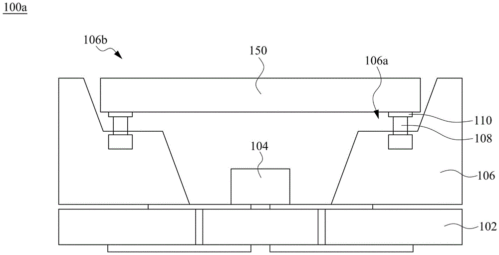
请参照图1,其绘示依照本发明的第一实施例的一种发光二极管封装结构的剖面图。发光二极管封装结构100a包括电路基板102、反射杯106、发光二极管芯片104以及透镜结构150。反射杯106设置于电路基板102上且与电路基板102共同构成一凹杯且形成一开口106b。反射杯106具有第一金属环108位于凹杯内。发光二极管芯片104固晶于凹杯内的电路基板102上。透镜结构150具有第二金属环110用以接合第一金属环108而覆盖开口106b。Please refer to FIG. 1 , which shows a cross-sectional view of a light emitting diode package structure according to a first embodiment of the present invention. The
在本实施例中,反射杯106的材质可以是高分子类如PE、PT、PC、PMMA、铁氟龙等各类塑胶橡胶产品,或为陶瓷如Al2O3、AlN、ZrO2…或金属如铁、铝、铜、不锈钢、或其他合金,但不以此为限。In this embodiment, the
在本实施例中,金属环的材质可以是金属(例如铜、镍、金、银)或其合金(例如金锡合金、镍锡合金、锡银铜合金、铁钴镍合金等材质),但不以此为限。金属环表面镀层为镀金(例如镀钯、镍、或其他金属)、或亦可为金属氧化物或氮化物(例如如TiO2、TiN或其他氧化物如SiO2、BN…),亦可涂布抗氧化层,如OSP(Organic Solderability Preservative),有机保焊膜等类似材料,但不以此为限。In this embodiment, the material of the metal ring can be metal (such as copper, nickel, gold, silver) or its alloy (such as gold-tin alloy, nickel-tin alloy, tin-silver-copper alloy, iron-cobalt-nickel alloy and other materials), but Not limited to this. The surface coating of the metal ring is gold-plated (such as palladium, nickel, or other metals), or it can also be metal oxide or nitride (such as TiO 2 , TiN or other oxides such as SiO 2 , BN...), or it can be coated Anti-oxidation layer, such as OSP (Organic Solderability Preservative), organic solder protection film and similar materials, but not limited to this.
在本实施例中,透镜结构150可以是玻璃、石英、蓝宝石、氟化钙等对应波长的透明材料,亦可为有机材料PC、PMMA等,但不以此为限。In this embodiment, the
在本实施例中,透镜结构150是平透镜,但不以此为限。In this embodiment, the
在本实施例中,金属环之间的接合材料可以为金属膏(如锡膏、金锡膏)、玻璃膏等无机材料,亦可为环氧树酯、硅胶等高分子材料。In this embodiment, the bonding material between the metal rings can be inorganic materials such as metal paste (such as solder paste, gold solder paste), glass paste, or polymer materials such as epoxy resin and silica gel.
请参照图2,其绘示依照本发明的第二实施例的一种发光二极管封装结构的剖面图。发光二极管封装结构100b较前述发光二极管封装结构100a增加了金属环(112、114)。反射杯106的底面具有第三金属环112,电路基板102的顶面具有第四金属环114,用以接合第三金属环112。反射杯106的倾斜内表面具有光反射涂层107。在本实施例中,光反射涂层107包含金属反射层(如铝、银、金等),其最外层可涂布氧化物(如TiO2、SiO2等)保护,但不以此为限。Please refer to FIG. 2 , which shows a cross-sectional view of a light emitting diode packaging structure according to a second embodiment of the present invention. Compared with the aforementioned
请参照图3,其绘示依照本发明的第三实施例的一种发光二极管封装结构的剖面图。发光二极管封装结构100c与前述发光二极管封装结构100b的差异在于,第一、三金属环(108、112)是一体成型的结构,亦或第一、三金属环(108、112)通过连接环109连接,且所有连接环的直径皆相同。Please refer to FIG. 3 , which shows a cross-sectional view of a light emitting diode packaging structure according to a third embodiment of the present invention. The difference between the light emitting
请参照图4,其绘示依照本发明的第四实施例的一种发光二极管封装结构的剖面图。发光二极管封装结构100d与前述发光二极管封装结构100b的差异在于增加另一组第一、二、三、四金属环(108’、110’、112’、114’)。在本实施例中,第一、二金属环(108’、110’)的直径小于第一、二金属环(108、110)的直径,而第三、四金属环(112’、114’)的直径大于第三、四金属环(112、114)的直径,但不以此为限。当发光二极管封装结构100d使用高分子粘胶130接合其金属环时,高分子粘胶130可填充于不同直径的第一、二金属环(108、110、108’、110’)之间与不同直径的第三、四金属环(112、114、112’、114’)之间,借以避免发光二极管芯片104所发出的高能量光线的直接照射而劣化。Please refer to FIG. 4 , which shows a cross-sectional view of a light emitting diode packaging structure according to a fourth embodiment of the present invention. The difference between the
请参照图5,其绘示依照本发明的第五实施例的一种发光二极管封装结构的剖面图。发光二极管封装结构100e具体绘示使用金属膏120接合金属环的具体结构。使用金属膏120或其他无机材料取代有机高分子材料接合金属环的优点在于避免有机高分子材料遭高能量光线L攻击而劣化。Please refer to FIG. 5 , which shows a cross-sectional view of a light emitting diode package structure according to a fifth embodiment of the present invention. The
请参照图6,其绘示依照本发明的第六实施例的一种发光二极管封装结构的剖面图。发光二极管封装结构100f的电路基板102具有凸台102a可供发光二极管芯片104固晶于其上。凸台102a的顶面高于反射杯106与电路基板102之间的接合介面。当发光二极管封装结构100f使用高分子粘胶130接合其金属环时,凸台102a的高度避免发光二极管芯片104所发出的高能量光线L的直接照射高分子粘胶130。此外,当透镜结构150是内嵌于反射杯106的凹杯内的台阶106a上时,高分子粘胶130可填入于第一、二金属环(108、110)与反射杯106的内壁之间,借以增加胶合的面积。Please refer to FIG. 6 , which shows a cross-sectional view of a light emitting diode packaging structure according to a sixth embodiment of the present invention. The
请参照图7,绘示依照本发明的第七实施例的一种发光二极管封装结构的剖面图。发光二极管封装结构100g与前述发光二极管封装结构100b的差异在于,透镜结构150是凸透镜,不同于前述的平透镜。Please refer to FIG. 7 , which shows a cross-sectional view of a light emitting diode packaging structure according to a seventh embodiment of the present invention. The difference between the
请参照图8,其绘示依照本发明的实施例的发光二极管封装结构的各种金属环的上视平面图。上述金属环的外形可为连续封闭的矩形9a、圆形9c或多边形9e,亦或为不连续的矩形9b、圆形9d或多边形9f等,但不以此为限。Please refer to FIG. 8 , which shows a top plan view of various metal rings of the LED packaging structure according to an embodiment of the present invention. The shape of the metal ring can be a continuous
综上所述,本发明的的发光二极管封装结构采多件式组合设计并以金属环接结各组件,解决基板不平整的问题,增加共晶良率。发光二极管封装结构可运用于多种基板以及各式透境,增加设计自由度。此外,金属环可阻挡接合胶材遭发光二极管的高能量光线攻击。To sum up, the LED packaging structure of the present invention adopts a multi-piece assembly design and connects each component with a metal ring, so as to solve the problem of unevenness of the substrate and increase the eutectic yield. The light-emitting diode packaging structure can be applied to various substrates and various transparent environments, increasing the degree of design freedom. In addition, the metal ring prevents the bonding adhesive from being attacked by the high-energy light of the LED.
虽然本发明已以实施方式揭露如上,然其并非用以限定本发明,任何熟悉此技艺者,于不脱离本发明的精神和范围内,当可作各种的更动与润饰,因此本发明的保护范围当视所附的权利要求书所界定的范围为准。Although the present invention has been disclosed above in terms of implementation, it is not intended to limit the present invention. Any skilled person may make various changes and modifications without departing from the spirit and scope of the present invention. Therefore, the present invention The scope of protection should be based on the scope defined by the appended claims.
Claims (15)
Priority Applications (3)
| Application Number | Priority Date | Filing Date | Title |
|---|---|---|---|
| CN202010165904.5A CN113394320B (en) | 2020-03-11 | 2020-03-11 | Light emitting diode packaging structure |
| US17/195,539 US11670748B2 (en) | 2020-03-11 | 2021-03-08 | LED package structure |
| EP21161826.9A EP3879587A1 (en) | 2020-03-11 | 2021-03-10 | Led package structure |
Applications Claiming Priority (1)
| Application Number | Priority Date | Filing Date | Title |
|---|---|---|---|
| CN202010165904.5A CN113394320B (en) | 2020-03-11 | 2020-03-11 | Light emitting diode packaging structure |
Publications (2)
| Publication Number | Publication Date |
|---|---|
| CN113394320A CN113394320A (en) | 2021-09-14 |
| CN113394320B true CN113394320B (en) | 2023-04-07 |
Family
ID=74870743
Family Applications (1)
| Application Number | Title | Priority Date | Filing Date |
|---|---|---|---|
| CN202010165904.5A Active CN113394320B (en) | 2020-03-11 | 2020-03-11 | Light emitting diode packaging structure |
Country Status (3)
| Country | Link |
|---|---|
| US (1) | US11670748B2 (en) |
| EP (1) | EP3879587A1 (en) |
| CN (1) | CN113394320B (en) |
Families Citing this family (1)
| Publication number | Priority date | Publication date | Assignee | Title |
|---|---|---|---|---|
| DE102021109968A1 (en) * | 2021-04-20 | 2022-10-20 | OSRAM Opto Semiconductors Gesellschaft mit beschränkter Haftung | Optoelectronic semiconductor component |
Citations (1)
| Publication number | Priority date | Publication date | Assignee | Title |
|---|---|---|---|---|
| JP2004146466A (en) * | 2002-10-22 | 2004-05-20 | Kyocera Corp | Lid and package for housing optical device using the same |
Family Cites Families (20)
| Publication number | Priority date | Publication date | Assignee | Title |
|---|---|---|---|---|
| JP2006269485A (en) * | 2005-03-22 | 2006-10-05 | Ngk Spark Plug Co Ltd | Light-emitting element mounting wiring board |
| US7528422B2 (en) | 2006-01-20 | 2009-05-05 | Hymite A/S | Package for a light emitting element with integrated electrostatic discharge protection |
| DE102008021436A1 (en) | 2008-04-29 | 2010-05-20 | Schott Ag | Optic converter system for (W) LEDs |
| CN201307605Y (en) | 2008-12-05 | 2009-09-09 | 弘凯光电(深圳)有限公司 | LED packaging structure |
| EP2472613B1 (en) | 2009-08-27 | 2018-11-28 | Kyocera Corporation | Light-emitting device |
| US20130050227A1 (en) | 2011-08-30 | 2013-02-28 | Qualcomm Mems Technologies, Inc. | Glass as a substrate material and a final package for mems and ic devices |
| KR20130059875A (en) * | 2011-11-29 | 2013-06-07 | 서울옵토디바이스주식회사 | Light emitting diode package |
| CN103137833A (en) * | 2013-03-15 | 2013-06-05 | 深圳市瑞丰光电子股份有限公司 | Method and structure of light emitting diode (LED) packaging |
| CN104851904B (en) * | 2015-05-13 | 2018-01-19 | 合肥鑫晟光电科技有限公司 | A kind of organic EL display panel, its preparation method and display device |
| JP6668022B2 (en) * | 2015-09-17 | 2020-03-18 | 日機装株式会社 | Light emitting module and method of manufacturing light emitting module |
| CN105845814B (en) * | 2016-05-04 | 2019-03-05 | 华中科技大学 | A kind of ultraviolet LED packaging structure and manufacturing method thereof |
| CN205692861U (en) * | 2016-06-17 | 2016-11-16 | 厦门市三安光电科技有限公司 | A kind of UV LED encapsulating structure |
| CN106449542B (en) * | 2016-08-26 | 2019-08-23 | 深圳市五矿发光材料有限公司 | A packaging structure of a semiconductor light-emitting chip with a window, airtight and silicone-free |
| JP6294419B2 (en) | 2016-09-01 | 2018-03-14 | 日機装株式会社 | Optical semiconductor device and method of manufacturing optical semiconductor device |
| JP6294418B2 (en) | 2016-09-01 | 2018-03-14 | 日機装株式会社 | Optical semiconductor device and method of manufacturing optical semiconductor device |
| CN206098446U (en) * | 2016-09-30 | 2017-04-12 | 鸿利智汇集团股份有限公司 | LED packaging structure |
| TWM544124U (en) | 2017-03-08 | 2017-06-21 | Ecocera Optronics Co Ltd | LED lead frame structure |
| KR102624113B1 (en) * | 2018-06-08 | 2024-01-12 | 서울바이오시스 주식회사 | Light emitting device package and manufacturing method thereof |
| CN209150148U (en) | 2018-12-13 | 2019-07-23 | 佛山市国星光电股份有限公司 | Supporting structure, LED component, support array and lamp group array |
| CN109509825A (en) * | 2018-12-13 | 2019-03-22 | 佛山市国星光电股份有限公司 | LED component and lamp group array |
-
2020
- 2020-03-11 CN CN202010165904.5A patent/CN113394320B/en active Active
-
2021
- 2021-03-08 US US17/195,539 patent/US11670748B2/en active Active
- 2021-03-10 EP EP21161826.9A patent/EP3879587A1/en active Pending
Patent Citations (1)
| Publication number | Priority date | Publication date | Assignee | Title |
|---|---|---|---|---|
| JP2004146466A (en) * | 2002-10-22 | 2004-05-20 | Kyocera Corp | Lid and package for housing optical device using the same |
Also Published As
| Publication number | Publication date |
|---|---|
| CN113394320A (en) | 2021-09-14 |
| US11670748B2 (en) | 2023-06-06 |
| EP3879587A1 (en) | 2021-09-15 |
| US20210288233A1 (en) | 2021-09-16 |
Similar Documents
| Publication | Publication Date | Title |
|---|---|---|
| TWI422069B (en) | Semiconductor device and method of manufacturing same | |
| CN107195751B (en) | Light emitting diode packaging structure | |
| CN101313415B (en) | Light emitting device and manufacturing method thereof | |
| JP5673190B2 (en) | Light emitting device | |
| CN105655464B (en) | Light emitting device package | |
| CN101926014A (en) | Semiconductor device package | |
| CN1976079A (en) | Light emitting device and method for manufacturing light emitting device | |
| CN103296174B (en) | The wafer-level package structure of a kind of LED flip chip, method and product | |
| CN101567366A (en) | Light emitting diode | |
| CN206432286U (en) | Light-emitting element package base structure | |
| CN113725346A (en) | Mini LED backlight source, backlight module and manufacturing method thereof | |
| TW201314972A (en) | Light-emitting diode package structure and manufacturing method thereof | |
| CN103904072A (en) | High-power LED chip integrated packaging structure | |
| JP6596410B2 (en) | Chip scale package light emitting device and manufacturing method thereof | |
| TWM549964U (en) | Light-emitting diode package structure with surface light source | |
| CN107123721B (en) | A kind of encapsulation structure and encapsulation method of LED with lens | |
| CN113394320B (en) | Light emitting diode packaging structure | |
| CN101779300A (en) | Light-emitting device | |
| CN103000786B (en) | White light emitting diode | |
| CN102646779B (en) | Ceramic-based power type light-emitting diode and packaging method thereof | |
| CN201152507Y (en) | Light emitting diode lamp | |
| TWI352419B (en) | Light emitting unit | |
| CN110808321A (en) | Ultraviolet light LED packaging structure | |
| CN203351661U (en) | Wafer level packaging structure for LED flip chip | |
| CN217280837U (en) | Nano-copper electrode all-copper bonded inverted UV-LED packaging structure |
Legal Events
| Date | Code | Title | Description |
|---|---|---|---|
| PB01 | Publication | ||
| PB01 | Publication | ||
| SE01 | Entry into force of request for substantive examination | ||
| SE01 | Entry into force of request for substantive examination | ||
| GR01 | Patent grant | ||
| GR01 | Patent grant |